WO2017179221A1 - Surface-coated cutting tool and manufacturing method therefor - Google Patents
Surface-coated cutting tool and manufacturing method therefor Download PDFInfo
- Publication number
- WO2017179221A1 WO2017179221A1 PCT/JP2016/068502 JP2016068502W WO2017179221A1 WO 2017179221 A1 WO2017179221 A1 WO 2017179221A1 JP 2016068502 W JP2016068502 W JP 2016068502W WO 2017179221 A1 WO2017179221 A1 WO 2017179221A1
- Authority
- WO
- WIPO (PCT)
- Prior art keywords
- grain boundary
- layer
- crystal
- hard layer
- type
- Prior art date
Links
Images


Classifications
-
- C—CHEMISTRY; METALLURGY
- C23—COATING METALLIC MATERIAL; COATING MATERIAL WITH METALLIC MATERIAL; CHEMICAL SURFACE TREATMENT; DIFFUSION TREATMENT OF METALLIC MATERIAL; COATING BY VACUUM EVAPORATION, BY SPUTTERING, BY ION IMPLANTATION OR BY CHEMICAL VAPOUR DEPOSITION, IN GENERAL; INHIBITING CORROSION OF METALLIC MATERIAL OR INCRUSTATION IN GENERAL
- C23C—COATING METALLIC MATERIAL; COATING MATERIAL WITH METALLIC MATERIAL; SURFACE TREATMENT OF METALLIC MATERIAL BY DIFFUSION INTO THE SURFACE, BY CHEMICAL CONVERSION OR SUBSTITUTION; COATING BY VACUUM EVAPORATION, BY SPUTTERING, BY ION IMPLANTATION OR BY CHEMICAL VAPOUR DEPOSITION, IN GENERAL
- C23C16/00—Chemical coating by decomposition of gaseous compounds, without leaving reaction products of surface material in the coating, i.e. chemical vapour deposition [CVD] processes
- C23C16/22—Chemical coating by decomposition of gaseous compounds, without leaving reaction products of surface material in the coating, i.e. chemical vapour deposition [CVD] processes characterised by the deposition of inorganic material, other than metallic material
- C23C16/30—Deposition of compounds, mixtures or solid solutions, e.g. borides, carbides, nitrides
- C23C16/34—Nitrides
-
- B—PERFORMING OPERATIONS; TRANSPORTING
- B23—MACHINE TOOLS; METAL-WORKING NOT OTHERWISE PROVIDED FOR
- B23B—TURNING; BORING
- B23B27/00—Tools for turning or boring machines; Tools of a similar kind in general; Accessories therefor
- B23B27/14—Cutting tools of which the bits or tips or cutting inserts are of special material
-
- C—CHEMISTRY; METALLURGY
- C23—COATING METALLIC MATERIAL; COATING MATERIAL WITH METALLIC MATERIAL; CHEMICAL SURFACE TREATMENT; DIFFUSION TREATMENT OF METALLIC MATERIAL; COATING BY VACUUM EVAPORATION, BY SPUTTERING, BY ION IMPLANTATION OR BY CHEMICAL VAPOUR DEPOSITION, IN GENERAL; INHIBITING CORROSION OF METALLIC MATERIAL OR INCRUSTATION IN GENERAL
- C23C—COATING METALLIC MATERIAL; COATING MATERIAL WITH METALLIC MATERIAL; SURFACE TREATMENT OF METALLIC MATERIAL BY DIFFUSION INTO THE SURFACE, BY CHEMICAL CONVERSION OR SUBSTITUTION; COATING BY VACUUM EVAPORATION, BY SPUTTERING, BY ION IMPLANTATION OR BY CHEMICAL VAPOUR DEPOSITION, IN GENERAL
- C23C16/00—Chemical coating by decomposition of gaseous compounds, without leaving reaction products of surface material in the coating, i.e. chemical vapour deposition [CVD] processes
- C23C16/02—Pretreatment of the material to be coated
- C23C16/0272—Deposition of sub-layers, e.g. to promote the adhesion of the main coating
-
- C—CHEMISTRY; METALLURGY
- C23—COATING METALLIC MATERIAL; COATING MATERIAL WITH METALLIC MATERIAL; CHEMICAL SURFACE TREATMENT; DIFFUSION TREATMENT OF METALLIC MATERIAL; COATING BY VACUUM EVAPORATION, BY SPUTTERING, BY ION IMPLANTATION OR BY CHEMICAL VAPOUR DEPOSITION, IN GENERAL; INHIBITING CORROSION OF METALLIC MATERIAL OR INCRUSTATION IN GENERAL
- C23C—COATING METALLIC MATERIAL; COATING MATERIAL WITH METALLIC MATERIAL; SURFACE TREATMENT OF METALLIC MATERIAL BY DIFFUSION INTO THE SURFACE, BY CHEMICAL CONVERSION OR SUBSTITUTION; COATING BY VACUUM EVAPORATION, BY SPUTTERING, BY ION IMPLANTATION OR BY CHEMICAL VAPOUR DEPOSITION, IN GENERAL
- C23C16/00—Chemical coating by decomposition of gaseous compounds, without leaving reaction products of surface material in the coating, i.e. chemical vapour deposition [CVD] processes
- C23C16/22—Chemical coating by decomposition of gaseous compounds, without leaving reaction products of surface material in the coating, i.e. chemical vapour deposition [CVD] processes characterised by the deposition of inorganic material, other than metallic material
- C23C16/30—Deposition of compounds, mixtures or solid solutions, e.g. borides, carbides, nitrides
- C23C16/36—Carbonitrides
-
- C—CHEMISTRY; METALLURGY
- C23—COATING METALLIC MATERIAL; COATING MATERIAL WITH METALLIC MATERIAL; CHEMICAL SURFACE TREATMENT; DIFFUSION TREATMENT OF METALLIC MATERIAL; COATING BY VACUUM EVAPORATION, BY SPUTTERING, BY ION IMPLANTATION OR BY CHEMICAL VAPOUR DEPOSITION, IN GENERAL; INHIBITING CORROSION OF METALLIC MATERIAL OR INCRUSTATION IN GENERAL
- C23C—COATING METALLIC MATERIAL; COATING MATERIAL WITH METALLIC MATERIAL; SURFACE TREATMENT OF METALLIC MATERIAL BY DIFFUSION INTO THE SURFACE, BY CHEMICAL CONVERSION OR SUBSTITUTION; COATING BY VACUUM EVAPORATION, BY SPUTTERING, BY ION IMPLANTATION OR BY CHEMICAL VAPOUR DEPOSITION, IN GENERAL
- C23C16/00—Chemical coating by decomposition of gaseous compounds, without leaving reaction products of surface material in the coating, i.e. chemical vapour deposition [CVD] processes
- C23C16/44—Chemical coating by decomposition of gaseous compounds, without leaving reaction products of surface material in the coating, i.e. chemical vapour deposition [CVD] processes characterised by the method of coating
- C23C16/455—Chemical coating by decomposition of gaseous compounds, without leaving reaction products of surface material in the coating, i.e. chemical vapour deposition [CVD] processes characterised by the method of coating characterised by the method used for introducing gases into reaction chamber or for modifying gas flows in reaction chamber
- C23C16/45523—Pulsed gas flow or change of composition over time
-
- C—CHEMISTRY; METALLURGY
- C23—COATING METALLIC MATERIAL; COATING MATERIAL WITH METALLIC MATERIAL; CHEMICAL SURFACE TREATMENT; DIFFUSION TREATMENT OF METALLIC MATERIAL; COATING BY VACUUM EVAPORATION, BY SPUTTERING, BY ION IMPLANTATION OR BY CHEMICAL VAPOUR DEPOSITION, IN GENERAL; INHIBITING CORROSION OF METALLIC MATERIAL OR INCRUSTATION IN GENERAL
- C23C—COATING METALLIC MATERIAL; COATING MATERIAL WITH METALLIC MATERIAL; SURFACE TREATMENT OF METALLIC MATERIAL BY DIFFUSION INTO THE SURFACE, BY CHEMICAL CONVERSION OR SUBSTITUTION; COATING BY VACUUM EVAPORATION, BY SPUTTERING, BY ION IMPLANTATION OR BY CHEMICAL VAPOUR DEPOSITION, IN GENERAL
- C23C28/00—Coating for obtaining at least two superposed coatings either by methods not provided for in a single one of groups C23C2/00 - C23C26/00 or by combinations of methods provided for in subclasses C23C and C25C or C25D
- C23C28/04—Coating for obtaining at least two superposed coatings either by methods not provided for in a single one of groups C23C2/00 - C23C26/00 or by combinations of methods provided for in subclasses C23C and C25C or C25D only coatings of inorganic non-metallic material
- C23C28/042—Coating for obtaining at least two superposed coatings either by methods not provided for in a single one of groups C23C2/00 - C23C26/00 or by combinations of methods provided for in subclasses C23C and C25C or C25D only coatings of inorganic non-metallic material including a refractory ceramic layer, e.g. refractory metal oxides, ZrO2, rare earth oxides
-
- C—CHEMISTRY; METALLURGY
- C23—COATING METALLIC MATERIAL; COATING MATERIAL WITH METALLIC MATERIAL; CHEMICAL SURFACE TREATMENT; DIFFUSION TREATMENT OF METALLIC MATERIAL; COATING BY VACUUM EVAPORATION, BY SPUTTERING, BY ION IMPLANTATION OR BY CHEMICAL VAPOUR DEPOSITION, IN GENERAL; INHIBITING CORROSION OF METALLIC MATERIAL OR INCRUSTATION IN GENERAL
- C23C—COATING METALLIC MATERIAL; COATING MATERIAL WITH METALLIC MATERIAL; SURFACE TREATMENT OF METALLIC MATERIAL BY DIFFUSION INTO THE SURFACE, BY CHEMICAL CONVERSION OR SUBSTITUTION; COATING BY VACUUM EVAPORATION, BY SPUTTERING, BY ION IMPLANTATION OR BY CHEMICAL VAPOUR DEPOSITION, IN GENERAL
- C23C28/00—Coating for obtaining at least two superposed coatings either by methods not provided for in a single one of groups C23C2/00 - C23C26/00 or by combinations of methods provided for in subclasses C23C and C25C or C25D
- C23C28/04—Coating for obtaining at least two superposed coatings either by methods not provided for in a single one of groups C23C2/00 - C23C26/00 or by combinations of methods provided for in subclasses C23C and C25C or C25D only coatings of inorganic non-metallic material
- C23C28/044—Coating for obtaining at least two superposed coatings either by methods not provided for in a single one of groups C23C2/00 - C23C26/00 or by combinations of methods provided for in subclasses C23C and C25C or C25D only coatings of inorganic non-metallic material coatings specially adapted for cutting tools or wear applications
-
- C—CHEMISTRY; METALLURGY
- C23—COATING METALLIC MATERIAL; COATING MATERIAL WITH METALLIC MATERIAL; CHEMICAL SURFACE TREATMENT; DIFFUSION TREATMENT OF METALLIC MATERIAL; COATING BY VACUUM EVAPORATION, BY SPUTTERING, BY ION IMPLANTATION OR BY CHEMICAL VAPOUR DEPOSITION, IN GENERAL; INHIBITING CORROSION OF METALLIC MATERIAL OR INCRUSTATION IN GENERAL
- C23C—COATING METALLIC MATERIAL; COATING MATERIAL WITH METALLIC MATERIAL; SURFACE TREATMENT OF METALLIC MATERIAL BY DIFFUSION INTO THE SURFACE, BY CHEMICAL CONVERSION OR SUBSTITUTION; COATING BY VACUUM EVAPORATION, BY SPUTTERING, BY ION IMPLANTATION OR BY CHEMICAL VAPOUR DEPOSITION, IN GENERAL
- C23C28/00—Coating for obtaining at least two superposed coatings either by methods not provided for in a single one of groups C23C2/00 - C23C26/00 or by combinations of methods provided for in subclasses C23C and C25C or C25D
- C23C28/40—Coatings including alternating layers following a pattern, a periodic or defined repetition
- C23C28/42—Coatings including alternating layers following a pattern, a periodic or defined repetition characterized by the composition of the alternating layers
-
- C—CHEMISTRY; METALLURGY
- C23—COATING METALLIC MATERIAL; COATING MATERIAL WITH METALLIC MATERIAL; CHEMICAL SURFACE TREATMENT; DIFFUSION TREATMENT OF METALLIC MATERIAL; COATING BY VACUUM EVAPORATION, BY SPUTTERING, BY ION IMPLANTATION OR BY CHEMICAL VAPOUR DEPOSITION, IN GENERAL; INHIBITING CORROSION OF METALLIC MATERIAL OR INCRUSTATION IN GENERAL
- C23C—COATING METALLIC MATERIAL; COATING MATERIAL WITH METALLIC MATERIAL; SURFACE TREATMENT OF METALLIC MATERIAL BY DIFFUSION INTO THE SURFACE, BY CHEMICAL CONVERSION OR SUBSTITUTION; COATING BY VACUUM EVAPORATION, BY SPUTTERING, BY ION IMPLANTATION OR BY CHEMICAL VAPOUR DEPOSITION, IN GENERAL
- C23C30/00—Coating with metallic material characterised only by the composition of the metallic material, i.e. not characterised by the coating process
- C23C30/005—Coating with metallic material characterised only by the composition of the metallic material, i.e. not characterised by the coating process on hard metal substrates
-
- B—PERFORMING OPERATIONS; TRANSPORTING
- B23—MACHINE TOOLS; METAL-WORKING NOT OTHERWISE PROVIDED FOR
- B23B—TURNING; BORING
- B23B2224/00—Materials of tools or workpieces composed of a compound including a metal
- B23B2224/24—Titanium aluminium nitride
-
- B—PERFORMING OPERATIONS; TRANSPORTING
- B23—MACHINE TOOLS; METAL-WORKING NOT OTHERWISE PROVIDED FOR
- B23B—TURNING; BORING
- B23B2228/00—Properties of materials of tools or workpieces, materials of tools or workpieces applied in a specific manner
- B23B2228/04—Properties of materials of tools or workpieces, materials of tools or workpieces applied in a specific manner applied by chemical vapour deposition [CVD]
-
- B—PERFORMING OPERATIONS; TRANSPORTING
- B23—MACHINE TOOLS; METAL-WORKING NOT OTHERWISE PROVIDED FOR
- B23B—TURNING; BORING
- B23B2228/00—Properties of materials of tools or workpieces, materials of tools or workpieces applied in a specific manner
- B23B2228/10—Coatings
- B23B2228/105—Coatings with specified thickness
-
- B—PERFORMING OPERATIONS; TRANSPORTING
- B23—MACHINE TOOLS; METAL-WORKING NOT OTHERWISE PROVIDED FOR
- B23C—MILLING
- B23C2224/00—Materials of tools or workpieces composed of a compound including a metal
- B23C2224/24—Titanium aluminium nitride (TiAlN)
-
- B—PERFORMING OPERATIONS; TRANSPORTING
- B23—MACHINE TOOLS; METAL-WORKING NOT OTHERWISE PROVIDED FOR
- B23C—MILLING
- B23C2228/00—Properties of materials of tools or workpieces, materials of tools or workpieces applied in a specific manner
- B23C2228/10—Coating
-
- C—CHEMISTRY; METALLURGY
- C23—COATING METALLIC MATERIAL; COATING MATERIAL WITH METALLIC MATERIAL; CHEMICAL SURFACE TREATMENT; DIFFUSION TREATMENT OF METALLIC MATERIAL; COATING BY VACUUM EVAPORATION, BY SPUTTERING, BY ION IMPLANTATION OR BY CHEMICAL VAPOUR DEPOSITION, IN GENERAL; INHIBITING CORROSION OF METALLIC MATERIAL OR INCRUSTATION IN GENERAL
- C23C—COATING METALLIC MATERIAL; COATING MATERIAL WITH METALLIC MATERIAL; SURFACE TREATMENT OF METALLIC MATERIAL BY DIFFUSION INTO THE SURFACE, BY CHEMICAL CONVERSION OR SUBSTITUTION; COATING BY VACUUM EVAPORATION, BY SPUTTERING, BY ION IMPLANTATION OR BY CHEMICAL VAPOUR DEPOSITION, IN GENERAL
- C23C28/00—Coating for obtaining at least two superposed coatings either by methods not provided for in a single one of groups C23C2/00 - C23C26/00 or by combinations of methods provided for in subclasses C23C and C25C or C25D
- C23C28/30—Coatings combining at least one metallic layer and at least one inorganic non-metallic layer
- C23C28/34—Coatings combining at least one metallic layer and at least one inorganic non-metallic layer including at least one inorganic non-metallic material layer, e.g. metal carbide, nitride, boride, silicide layer and their mixtures, enamels, phosphates and sulphates
- C23C28/347—Coatings combining at least one metallic layer and at least one inorganic non-metallic layer including at least one inorganic non-metallic material layer, e.g. metal carbide, nitride, boride, silicide layer and their mixtures, enamels, phosphates and sulphates with layers adapted for cutting tools or wear applications
Definitions
- the present invention relates to a surface-coated cutting tool and a manufacturing method thereof.
- This application claims priority based on Japanese Patent Application No. 2016-081095 filed on Apr. 14, 2016, and incorporates all the description content described in the above Japanese application.
- Cutting tools made of cemented carbide often have problems that the cutting edge is worn or chipped because the cutting edge is exposed to a severe environment such as high temperature and high load during cutting. For this reason, development of the coating which coat
- a film made of a compound of titanium (Ti) and aluminum (Al) and / or nitrogen (N) and / or carbon (C) (hereinafter also referred to as AlTiN, AlTiCN, etc.) has high hardness. It is known that oxidation resistance can be improved by increasing the Al content. Improvement of the performance of the cutting tool is expected by coating the cutting tool with such a coating.
- Non-Patent Document 1 when Ikeda et al. (Non-Patent Document 1) produced a film of “AlTiN” or “AlTiCN” with an atomic ratio of Al exceeding 0.7 by a physical vapor deposition (PVD) method, It points out that the hardness decreases due to the phase transition of the structure to the wurtzite crystal structure.
- Setoyama et al. (Non-Patent Document 2) produced a TiN / AlN super-multilayer film by the PVD method in order to increase the Al content in the coating of “AlTiN” or “AlTiCN”.
- Patent Document 1 Japanese Patent Laying-Open No. 2015-193071
- Patent Document 1 is a hard coating layer formed by a CVD method and is represented by (Ti 1-x Al x ) (C y N 1-y ).
- a composite nitride layer or a composite carbonitride layer is included, the layer includes crystal grains having a cubic structure, and the composition of Ti and Al periodically changes along the normal direction of the surface of the tool substrate.
- a hard coating layer is disclosed.
- a surface-coated cutting tool is a surface-coated cutting tool including a substrate and a coating formed on the substrate, the coating including a hard layer, and the hard layer is chlorinated.
- a second layer made of an object (where x ⁇ y) is alternately laminated, and the total thickness of the adjacent first layer and second layer is 3 nm or more and 40 nm or less, and is a hard layer
- the plane normal to the (111) plane which is the crystal plane of the crystal grain, by analyzing the crystal orientation of each of the plurality of crystal grains with respect to a plane parallel to the surface of the substrate using an electron beam backscattering diffractometer When the crossing angle between the direction and the normal direction to the surface of the substrate is measured, the crossing angle
- the manufacturing method of the surface coating cutting tool which concerns on 1 aspect of this invention is a manufacturing method of said surface coating cutting tool, Comprising: The 1st process which prepares a base material, A chemical vapor deposition (CVD) method is used for a hard layer.
- the second step includes the step of modulating the flow rate of either or both of the AlCl 3 gas and the TiCl 4 gas.
- Patent Document 1 the composite nitride layer or the composite carbonitride layer has a cubic structure, and the composition of Ti and Al periodically changes along the normal direction of the substrate, thereby achieving high hardness and toughness. It is said that an excellent hard coating layer was realized. However, this hard coating layer has room for improvement, particularly in obtaining chipping resistance. Therefore, it has not yet achieved the long life required by having both the high wear resistance and the high chipping resistance, and its development is eagerly desired.
- the present invention has been made in view of the above circumstances, and an object thereof is to provide a surface-coated cutting tool that exhibits particularly high wear resistance while exhibiting high chipping resistance, and a method for manufacturing the same. [Effects of the present disclosure] According to the above, it is possible to provide a surface-coated cutting tool that exhibits particularly high wear resistance while exhibiting high chipping resistance.
- a surface-coated cutting tool is a surface-coated cutting tool including a base material and a coating film formed on the base material, the coating film including a hard layer, and the hard layer Includes a plurality of crystal grains having a sodium chloride type crystal structure, and the crystal grains include a first layer made of a nitride or carbonitride of Al x Ti 1-x, and a nitride of Aly Ti 1-y Alternatively, it has a laminated structure in which second layers made of carbonitride (however, x ⁇ y) are alternately laminated, and the total thickness of the adjacent first layer and second layer is 3 nm or more and 40 nm or less.
- (111) plane which is a crystal plane of a crystal grain by analyzing each crystal orientation of a plurality of crystal grains using an electron beam backscattering diffraction device with respect to a plane parallel to the surface of a base material in a hard layer
- Area ratio of 0 degrees 10 degrees below become crystal grains is 40% or more.
- the grain boundary includes a CSL grain boundary and a general grain boundary, and the length of the ⁇ 3-type grain boundary among the CSL grain boundaries constitutes the CSL grain boundary.
- the crystal grains have a particle size of 1 ⁇ m or less. Thereby, the hardness of the surface-coated cutting tool is further improved.
- the hard layer has a thickness of 1 ⁇ m or more and 15 ⁇ m or less. Thereby, chipping resistance can be improved while maintaining the wear resistance of the surface-coated cutting tool.
- the hard layer has an indentation hardness of 30 GPa or more and 40 GPa or less by a nanoindentation method. This further improves the wear resistance of the surface-coated cutting tool.
- the hard layer has an absolute value of compressive residual stress of 0.5 GPa to 3.0 GPa. This further improves the toughness of the surface-coated cutting tool.
- a method for manufacturing a surface-coated cutting tool according to an aspect of the present invention is the above-described method for manufacturing a surface-coated cutting tool, wherein a first step of preparing a base material and a hard layer using a CVD method are prepared. A second step of forming, and the second step includes a step of modulating the flow rate of either or both of the AlCl 3 gas and the TiCl 4 gas.
- the notation in the form of “A to B” in the present specification means the upper and lower limits of the range (that is, not less than A and not more than B), and no unit is described in A, and only a unit is described in B. In this case, the unit of A and the unit of B are the same.
- a compound or the like when a compound or the like is represented by a chemical formula, when the atomic ratio is not particularly limited, it includes any conventionally known atomic ratio, and is not necessarily limited to a stoichiometric range.
- the surface-coated cutting tool includes a base material and a film formed on the base material.
- the coating preferably covers the entire surface of the substrate. However, even if a part of the substrate is not coated with this coating or the configuration of the coating is partially different, it does not depart from the scope of the present invention.
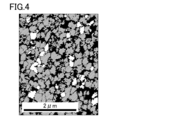
- FIG. 1 is a photograph of a microscopic image of a cross-section of a film in a surface-coated cutting tool.
- a coating 20 is provided on a substrate 10, and the coating 20 is composed of a hard layer.
- the surface-coated cutting tool according to this embodiment can exhibit particularly high wear resistance while exhibiting high chipping resistance. For this reason, it is possible to exhibit high wear resistance based on high hardness and high chipping resistance based on excellent toughness, thereby realizing a long life. Therefore, drills, end mills, drill tip replacement cutting tips, end mill tip replacement cutting tips, milling tip replacement cutting tips, turning tip replacement cutting tips, metal saws, gear cutting tools, reamers, taps, etc. It can be suitably used as a cutting tool.
- any substrate can be used as long as it is conventionally known as this type of substrate.
- cemented carbide for example, WC-based cemented carbide, including WC, including Co or containing carbonitride such as Ti, Ta, Nb), cermet (TiC, TiN, TiCN, etc.) Main component
- high-speed steel ceramics (titanium carbide, silicon carbide, silicon nitride, aluminum nitride, aluminum oxide, etc.), cubic boron nitride sintered body, or diamond sintered body Is preferred.
- a cemented carbide particularly a WC-based cemented carbide, or a cermet (particularly a TiCN-based cermet).
- These base materials are particularly excellent in the balance between hardness and strength at high temperatures, and have excellent characteristics as base materials for surface-coated cutting tools for the above applications.
- the base material includes those having a chip breaker and those having no chip breaker.
- the shape of the edge of the cutting edge is sharp edge (the ridge where the rake face and flank face intersect), honing (the sharp edge is given a radius), negative land (the chamfered), honing and negative land combined. Any thing is included.
- the coating includes a hard layer.
- This hard layer may be included in the coating in one layer or two or more layers. It goes without saying that layers other than the hard layer may be included.
- the thickness of the coating is preferably 1 to 15 ⁇ m. When the thickness of the film is within this range, the characteristics of the film including the effect of improving the chipping resistance while maintaining the wear resistance of the hard layer can be suitably exhibited. If the thickness of the coating is less than 1 ⁇ m, the hardness tends to decrease, and if it exceeds 15 ⁇ m, the coating is easily peeled off from the substrate during cutting.
- the total thickness of the coating is preferably 3 to 7.5 ⁇ m from the viewpoint of improving the characteristics.
- the thickness of the coating is measured, for example, by obtaining a cross-sectional sample parallel to the normal direction of the surface of the substrate and observing the sample with a scanning transmission electron microscope (STEM).
- STEM high angle scattering dark field method HAADF-STEM: High-Angle Angular Dark-field Scanning Transmission Electron Microscopy
- the term “thickness” means an average thickness. Specifically, the observation magnification of the cross-sectional sample is set to 5000 to 10,000 times, the observation area is set to 100 to 500 ⁇ m 2 , the thickness width at 10 locations in one visual field is measured, and the average value is defined as “thickness”. The same applies to the thickness of each layer described later unless otherwise specified.
- the hard layer includes a plurality of crystal grains having a sodium chloride type crystal structure. It can be confirmed that the crystal grains contained in the hard layer have a sodium chloride type crystal structure using an X-ray diffractometer, a SEM-EBSD device, a TEM analyzer, or the like.
- the hard layer among the plurality of crystal grains confirmed in the observation region (100 ⁇ m ⁇ 100 ⁇ m) of the analyzer, 50 area% or more of crystal grains may have a sodium chloride type crystal structure. preferable. From the viewpoint of increasing the hardness of the hard layer, it is preferable that all the crystal grains contained in the hard layer are of a sodium chloride type.
- the crystal grains contained in the hard layer are composed of a first layer made of nitride or carbonitride of Al x Ti 1-x and a nitride or carbonitride of Al y Ti 1-y (where x ⁇ y).
- the second layer is a laminated structure in which one or more layers are alternately laminated.
- the composition of the first layer and the second layer may be either nitride or carbonitride. However, when the composition of the first layer is nitride, the composition of the second layer is also nitride. When the composition of the first layer is carbonitride, the composition of the second layer is also carbonitride.
- the crystal grains contained in the hard layer are each a single crystal or twin of AlTi nitride or carbonitride, and the atomic ratio of Al varies within the single crystal or twin. Yes. This variation is periodic and can be continuous or stepwise. As a result, the crystal grains included in the hard layer have a minute strain at a predetermined interface, and a laminated structure including a first layer and a second layer that can be distinguished as different layers based on the strain is formed. It becomes. And the hardness of a crystal grain improves with this distortion.
- FIG. 2 is a photograph showing an enlargement of a portion surrounded by a chain line in FIG.
- a white (light color) region is a region having a larger atomic ratio of Ti than a black (dark color) region. That is, it can be understood from FIG. 2 that Ti-rich white areas and Al-rich black areas exist alternately in the hard layer.
- the ⁇ 3 type grain boundary exists as a line symmetry axis in the crystal structure in the twin crystal, and the above-described stacked structure exists on both sides of this axis. preferable.
- the laminated structure can be stably grown over a long period.
- the atomic ratio x of Al in the first layer varies in the range of 0.6 or more and less than 1 in each first layer
- the atomic ratio y of Al in the second layer is 0. 0 in each second layer. It preferably varies within a range of 45 or more and less than 0.6. That is, the crystal grains contained in the hard layer fluctuate with the first layer in which the atomic ratio of Al is maintained to be high and the Al atomic ratio is relatively low in comparison with the first layer. It is preferable that the 2nd layer to have has the laminated structure arrange
- the atomic ratio x of Al in the first layer never becomes less than 0.6. This is because if the atomic ratio x is less than 0.6, it should be the Al atomic ratio y of the second layer. It is based on the same reason that atomic ratio y does not become 0.6 or more. The atomic ratio x does not become 1 because the first layer contains Ti. On the other hand, from the viewpoint of improving toughness while maintaining high wear resistance, the atomic ratio y is 0.45 or more. When the atomic ratio y is less than 0.45, the oxidation resistance becomes inferior due to the decrease in the amount of Al, and the toughness associated with the oxidation of the film tends to occur.
- the atomic ratio x and the atomic ratio y are obtained by obtaining a cross-sectional sample parallel to the normal direction of the surface of the substrate in the hard layer, and energy dispersive X-rays attached to the SEM or TEM with respect to the crystal grains appearing in the cross-sectional sample.
- EDX Energy Dispersive X-ray spectroscopy
- the atomic ratio at the analysis position can be calculated.
- the object for calculating the atomic ratio x and the atomic ratio y can be expanded to the entire surface of the cross-sectional sample, and therefore the atomic ratio x and The atomic ratio y can be specified.
- the maximum difference between the atomic ratio x and the atomic ratio y is 0.05 or more and 0.5 or less. Further, the maximum value of the difference between the atomic ratio x and the atomic ratio y is preferably 0.15 or more and 0.5 or less.
- the maximum value of the difference between the atomic ratio x and the atomic ratio y is less than 0.05, the strain in the crystal grains becomes small, and the hardness of the crystal grains tends to decrease.
- the maximum value of the difference exceeds 0.5, the strain in the crystal grains is too large and the lattice defects become large, so that the hardness of the crystal grains tends to decrease.
- the maximum value of the difference between the atomic ratio x and the atomic ratio y is calculated from the values of all the calculated atomic ratios x when the atomic ratio x and the atomic ratio y are calculated based on the cross-sectional sample by the above-described method. And the value obtained when the difference between the calculated maximum value of all the atomic ratios y and the minimum value is obtained. That is, it is synonymous with the value obtained when the difference between the maximum value of the atomic ratio x selected from the entire hard layer and the minimum value of the atomic ratio y is obtained.
- the total thickness (hereinafter also referred to as “lamination period”) of the adjacent first layer and second layer is 3 to 40 nm.
- laminate period the crystal grains have high hardness and toughness is improved.
- the total thickness of the adjacent first layer and second layer is preferably 7 to 38 nm.
- the adjacent first layer and second layer may have a thickness of at least one pair of 3 to 40 nm. However, it is preferable that all pairs of the adjacent first layer and second layer have a thickness of 3 to 40 nm, so that a film excellent in chipping resistance can be stably produced.
- the total thickness of the adjacent first layer and second layer is, for example, obtained by obtaining a cross-sectional sample at an arbitrary location (preferably in the vicinity of the edge of the cutting edge), and 10 sets of 10 crystal grains appearing in the cross section.
- the total thickness of the first layer and the second layer adjacent to each other can be measured, and the average value can be expressed as the total thickness.
- the observation magnification is set to 500,000 and the observation area is set to about 0.1 ⁇ m 2 so that one crystal grain appears in one visual field.
- Orientation of crystal grains In the hard layer, by analyzing the crystal orientation of each of the plurality of crystal grains using a backscatter diffraction (EBSD) device with respect to the surface of the hard layer parallel to the surface of the base material, Area ratio of crystal grains in which the crossing angle is 0 degree or more and less than 10 degrees when the crossing angle between the normal direction to the (111) plane which is the crystal plane of the crystal grain and the normal direction to the surface of the substrate is measured Is 40% or more.
- the hard layer satisfies this, the hard layer is particularly excellent in hardness, and thus can contribute to the excellent wear resistance of the surface-coated cutting tool.
- the upper limit of the area ratio is not particularly limited, and is preferably 100% from the viewpoint of improving hardness.
- the area ratio can be obtained as follows. First, a hard layer is formed on a substrate based on a manufacturing method described later. Next, the surface is parallel to the surface of the hard layer formed (the surface opposite to the surface located on the substrate side), and the thickness is 0.1 to 0 with respect to the depth direction from the surface. A processed surface which is a new surface obtained by removing the hard layer located in a region of 5 ⁇ m is prepared. This is because the vicinity of the surface of the hard layer has a large variation in crystal grains and is inappropriate as a position where the characteristics of the hard layer should be specified. Regarding the processing position, it can be set to an arbitrary position of the hard layer.
- FIB processing using FIB can be mentioned.
- FIB processing using FIB Flucused Ion Beam
- a processed surface that is parallel to the surface of the substrate and suitable for the EBSD analysis described later is obtained.
- the manufacturing method of the processed surface is not limited to FIB processing, but it is preferable that at least a measurement surface according to the processed surface manufactured by FIB processing can be manufactured.
- another layer such as a surface layer is formed on the hard layer, it is preferable to perform the FIB processing after removing the other layer by polishing or the like to expose the hard layer. .
- observation is performed using an FE-SEM equipped with EBSD, and EBSD analysis is performed on the obtained observation image.
- This observation can be performed by placing a focused electron beam individually on each pixel of the observation image and sequentially collecting EBSD data.
- the observation position is not particularly limited, but it is preferable to observe the vicinity of the edge of the edge of the blade in consideration of the relationship with the cutting characteristics.
- the EBSD device is based on automatic analysis of the Kikuchi diffraction pattern generated by backscattered electrons, and the crystal orientation in which crystal grains are oriented, and the crystal orientation is the normal direction of the measurement target surface (that is, the normal direction of the surface of the substrate) It is possible to measure the angle (intersection angle) at which the crossing is made. Using this, the measurement target surface is imaged using the above-described apparatus, and the intersection angle between the normal direction with respect to the (111) plane and the normal direction with respect to the surface of the substrate in each pixel of the captured image is measured.
- the normal of the measurement target surface is inclined by 70 ° with respect to the incident beam, and analysis is performed at 15 kV. In order to avoid the charging effect, a pressure of 10 Pa is applied.
- the high current mode is used in combination with the opening diameter of 60 ⁇ m or 120 ⁇ m.
- Data collection is performed in steps of 0.1 ⁇ m / step for 500 ⁇ 300 pixels corresponding to a surface area of 50 ⁇ 30 ⁇ m in the measurement target surface. Then, the pixels are divided into the following intersection angle ranges, and groups 1 to 18 are constructed.
- Crossing angle is 0 degree or more and less than 5 degree
- Group 2 Crossing angle is 5 degree or more and less than 10 degree
- Group 3 Crossing angle is 10 degree or more and less than 15 degree
- Group 4 Crossing angle is 15 degree or more and less than 20 degree
- Group 5 Crossing angle between 20 and 25 degrees
- Group 6 Crossing angle between 25 and 30 degrees
- Group 7 Crossing angle between 30 and 35 degrees
- Group 8 Crossing angle between 35 and 40 degrees
- Group 9 Crossing Angle 10 to 45 degrees
- Group 10 Crossing angle 45 to 50 degrees
- Group 11 Crossing angle 50 to 55 degrees
- Group 12 Crossing angle 55 to 60 degrees
- Group 13 Crossing angle 60 degrees or more and less than 65 degrees
- Group 14 Crossing angle 65 degrees or more and less than 70 degrees
- Group 16 Crossing angle 75 degrees or more and less than 80 degrees
- Group 18 Crossing angle is 85 degrees or more and less than 90
- the frequency which is the sum of the number of pixels in each of the groups 1 to 18 is calculated, and the frequency distribution of the intersection angles is calculated. That is, “frequency” corresponds to the sum of the crystal grain areas of each group when all crystal grains appearing on the measurement target surface are divided into groups 1 to 18 for each crossing angle.
- the grouping and the calculation of the intersection angle frequency distribution can be performed using, for example, commercially available software ("Orientation Imaging Microscopy Ver 6.2", manufactured by EDAX).
- the total frequency of groups 1 and 2 is 40% or more of the total frequency of all groups. Since such a hard layer can have extremely high hardness, the abrasion resistance of the coating can be improved.
- the total frequency of groups 1 and 2 is preferably 50% or more, more preferably 60% or more of the total frequency of all groups.
- FIG. 3 An example of a graph showing the frequency distribution of crossing angles is shown in FIG.
- the horizontal axis of this graph represents 18 groups into which the crystal grains are divided, and the vertical axis is the frequency.
- the total frequency of groups 1 and 2 is 59.8% of the total frequency of all groups.
- the grain boundaries of the crystal grains included in the hard layer include CSL grain boundaries (corresponding lattice crystal grain boundaries) and general grain boundaries, and the length of the ⁇ 3-type grain boundary among the CSL grain boundaries is CSL grain boundaries.
- ⁇ 3-type grain boundary ⁇ 5-type grain boundary, ⁇ 7-type grain boundary, ⁇ 9-type grain boundary, ⁇ 11-type grain boundary, ⁇ 13-type grain boundary, ⁇ 15-type grain boundary, ⁇ 17-type grain ⁇ 3-29 type, which is the total length of each of the boundary, ⁇ 19-type grain boundary, ⁇ 21-type grain boundary, ⁇ 23-type grain boundary, ⁇ 25-type grain boundary, ⁇ 27-type grain boundary, and ⁇ 29-type grain boundary It is preferably less than 50% of the length of the crystal grain boundary.
- the CSL grain boundary is characterized by a multiplicity index ⁇ , and corresponds to the case where the crystal lattice site densities of two crystal grains in contact with the crystal grain boundary are superimposed on both crystal lattices. It is defined as the ratio with the density of the part. For simple structures, it is generally accepted that low ⁇ value grain boundaries tend to have low interfacial energy and special properties. Therefore, the control of the ratio of the special grain boundaries and the distribution of grain orientation difference estimated from the CSL model is considered to be important for the characteristics of the ceramic coating and the method for improving these characteristics.
- the CSL grain boundaries are ⁇ 3 type grain boundaries, ⁇ 5 type crystal grain boundaries, ⁇ 7 type crystal grain boundaries, ⁇ 9 type crystal grain boundaries, ⁇ 11 type crystal grain boundaries, ⁇ 13 type crystal grain boundaries, and ⁇ 15 type crystal grains.
- the general grain boundary is a grain boundary other than the CSL grain boundary. Therefore, the general grain boundary is a remaining portion obtained by removing the CSL grain boundary from the whole grain boundary of the crystal grains when the cross section of the hard layer is observed by EBSD.
- the length of the ⁇ 3-type grain boundary means the total length of the ⁇ 3-type grain boundary in the field of view observed by EBSD
- the length of the ⁇ 3-29 type grain boundary means the length of the field of view observed by EBSD.
- ⁇ 3-type grain boundary, ⁇ 5-type grain boundary, ⁇ 7-type grain boundary, ⁇ 9-type grain boundary, ⁇ 11-type grain boundary, ⁇ 13-type grain boundary, ⁇ 15-type grain boundary, ⁇ 17-type grain boundary, ⁇ 19 The total length of each of the type grain boundaries, ⁇ 21 type grain boundaries, ⁇ 23 type crystal grain boundaries, ⁇ 25 type crystal grain boundaries, ⁇ 27 type crystal grain boundaries, and ⁇ 29 type crystal grain boundaries is shown.
- the ⁇ 3-type grain boundary is considered to have the lowest grain boundary energy among the CSL grain boundaries. Therefore, by increasing the proportion of the ⁇ 3-29 type grain boundary in the ⁇ 3-29 type grain boundary, mechanical properties (particularly plastic resistance) It is thought that (deformability) can be improved.
- the ⁇ 3 type grain boundary is a grain boundary having high consistency, the two crystal grains having the ⁇ 3 type grain boundary as the grain boundary exhibit a behavior similar to that of a single crystal or twin crystal, and are coarsened. Show a tendency to When the crystal grains are coarsened, film properties such as chipping resistance are deteriorated.
- the length of the ⁇ 3-type grain boundary is defined to be less than 50% of the length of the ⁇ 3-29 type grain boundary to suppress grain coarsening, thereby preventing chipping of the hard layer. Sex is guaranteed.
- the lower limit is preferably 20%. This is because a hard coating with uniform grain size and little variation in characteristics can be obtained.
- the length of the ⁇ 3-type grain boundary is less than 50% of the length of the ⁇ 3-29 type grain boundary can be confirmed as follows. First, it cut
- water-resistant abrasive paper containing a SiC abrasive as an abrasive
- the coating surface For example, after cutting the surface of the hard layer (if the other layer is formed on the hard layer, the coating surface) with a wax or the like on a sufficiently large holding plate. Then, cut with a rotary blade cutter in a direction perpendicular to the flat plate (cut so that the rotary blade and the flat plate are as vertical as possible). This is because the surface of the substrate and the surface of the hard layer (coating surface) are considered to be parallel. This cutting can be performed at any part of the hard layer as long as it is performed in such a vertical direction.
- the polishing is performed using the water-resistant abrasive papers # 400, # 800, and # 1500 in order (the number (#) of the water-resistant abrasive paper means a difference in the particle size of the abrasive, and the larger the number, the more abrasive particles. The diameter becomes smaller).
- the cross-section polished surface of the hard layer can be prepared. Then, this cross-section polished surface is used as a measurement target surface, and the measurement target surface is observed using an FE-SEM equipped with an EBSD device. In this observation, the vicinity of the interface on the substrate side of the hard layer and the vicinity of the interface on the surface side are excluded from the measurement target surface.
- the vicinity of the interface on the base material side of the hard layer is a portion formed at the initial stage of growth of the hard layer, and there is a large variation in crystal grains, which is inappropriate as a position where the characteristics of the hard layer should be specified.
- the observation magnification of the FE-SEM is appropriately selected from the range of 2000 to 20000 times, and the observation area is also appropriately selected from the range of 200 to 10000 ⁇ m 2. It is preferable that 10 to 100 crystal grains appear.
- the normal of the measurement target surface is inclined by 70 ° with respect to the incident beam, and analysis is performed at 15 kV. In order to avoid the charging effect, a pressure of 10 Pa is applied.
- the high current mode is used in combination with the opening diameter of 60 ⁇ m or 120 ⁇ m.
- Data collection is performed at a step of 0.1 ⁇ m / step for 500 ⁇ 300 points corresponding to a surface area of 50 ⁇ 30 ⁇ m on the polished surface.
- Noise filtering and grain boundary character distribution are determined using commercially available software ("orientation Imaging microscopy Ver 6.2", manufactured by EDAX). Analysis of grain boundary character distribution is based on data available from Grimmer (H. Grimmer, R. Bonnet, Philosophical Magazine A 61 (1990), 493-509).
- the special crystal grain boundaries corresponding to the ⁇ 3-type crystal grain boundaries are counted, the other special crystal grain boundaries are counted, and the ratio thereof is calculated. As a result, the ratio of the length of the ⁇ 3-type grain boundary to the length of the ⁇ 3-29 type grain boundary can be obtained.
- the crystal grains contained in the hard layer preferably have a grain size of 1 ⁇ m or less. Thereby, the hardness of a hard layer can further be improved.
- the grain size of the hard layer crystal grains can be determined using the above-described method of calculating the frequency distribution of the crossing angles.
- groups 1 to 18 are constructed by dividing the pixels for each intersection angle range by the same method as the calculation method of the intersection angle frequency distribution described above.
- a color map in which the color is changed for each intersection angle is created.
- the “Cristal Direction MAP” method included in the software can be used.
- the color map a region in which colors match (that is, groups match) and the periphery is surrounded by other colors (that is, other groups) is regarded as an individual region of each crystal grain.
- an imaginary diagonal line that can be drawn longest for each region is drawn, and this is used as the grain size of each crystal grain.
- FIG. 4 shows an example of a part of a color map created based on the analysis of the measurement target surface.
- a region surrounded by a solid line and indicated by hatching with hatching is a crystal grain having the crossing angle of 0 degree or more and less than 10 degrees.
- a white region surrounded by a solid line and not hatched is a crystal grain having the crossing angle of 10 degrees or more and less than 90 degrees.
- the region where the crystal orientation is not specified is shown in black.
- all of the observed crystal grains have a grain size of 1 ⁇ m or less.
- the particle size classification on the horizontal axis shows the range of 0 to 1 ⁇ m divided by 0.05 ⁇ m.
- 70 area% or more and 100 area% or less of the total area (100%) occupied by the crystal grains observed in the photographed image is a crystal grain having a particle diameter of 0.5 ⁇ m or less.
- the crystal grains contained in the hard layer preferably have an average aspect ratio A of 2 or more.
- the maximum width among the widths of the individual crystal grains that are perpendicular to the crystal growth direction is defined as the particle width w, and the maximum of the lengths that are perpendicular to the grain width w.
- the grain length is 1 and the ratio of l to w (l / w) is the aspect ratio ⁇ of each crystal grain.
- an average value of the aspect ratio ⁇ obtained for each crystal grain is an average aspect ratio A
- an average value of the particle width w obtained for each crystal grain is an average grain width W.
- the crystal grains contained in the hard layer have an average aspect ratio A of 2 or more and an average particle width W of 0.5 ⁇ m or less.
- the crystal grains satisfying the above conditions have a columnar structure, which can exhibit excellent chipping resistance and wear resistance. If the average aspect ratio A of the crystal grains exceeds 100, it is not preferable because cracks easily propagate along the interface between the first layer and the second layer and the crystal grain boundary between the crystal grains.
- the average aspect ratio A of the crystal grains is preferably 30 to 80, more preferably 40 to 60. If the average grain width W of the crystal grains is less than 0.1 ⁇ m, the wear resistance is lowered, which is not preferable. When the average grain width W of the crystal grains exceeds 1.0 ⁇ m, the toughness is lowered. Therefore, the average grain width W of the crystal grains contained in the hard layer is preferably 0.1 to 1.0 ⁇ m.
- the average grain width W of the crystal grains is more preferably 0.2 to 0.8 ⁇ m.
- the average aspect ratio A can be measured, for example, by observing the surface to be measured with a STEM in the same manner as when measuring the thickness of the first layer and the second layer in the crystal grains. For example, ten crystal grains appearing in a STEM microscopic image are selected, and the particle width w and the particle length l are specified for these crystal grains. Next, the ratio (l / w) is calculated as the aspect ratio ⁇ of each crystal grain, and the average value of the aspect ratio ⁇ is calculated. Note that excluding the vicinity of the two interfaces of the hard layer from the measurement target surface is the same as described above.
- the hard layer preferably has an indentation hardness of 30 to 40 GPa by a nanoindentation method. More preferably, it is 32-38 GPa.
- the indentation hardness of the hard layer by the nanoindentation method is in the above range, the surface-coated cutting tool according to this embodiment has improved wear resistance. In particular, excellent performance can be achieved when cutting difficult-to-cut materials such as heat-resistant alloys.
- the above indentation hardness can be measured by using an ultra-fine indentation hardness tester that can use the nanoindentation method. Specifically, the indentation hardness can be calculated based on the indentation depth in which the indenter is pushed in with a predetermined load (for example, 30 mN) perpendicular to the thickness direction of the hard layer. When another layer such as a surface coating layer is present on the hard layer, the hard layer is exposed except for the other layer by carrying out a calotest, oblique lapping, etc., and the above method is applied to the exposed hard layer. By using it, indentation hardness can be measured.
- a predetermined load for example, 30 mN
- the hard layer preferably has a compressive residual stress, and the residual stress preferably has an absolute value of 0.5 GPa to 3.0 GPa. That is, when the hard layer has compressive residual stress, the absolute value is preferably 3.0 GPa or less.
- the absolute value of the compressive residual stress of the hard layer is in the above range, the toughness of the hard layer can be dramatically improved.
- the absolute value of the compressive residual stress exceeds 3.0 GPa, the wear resistance tends to decrease with the destruction of the structure. If the absolute value of the compressive residual stress is less than 0.5 GPa, chipping tends to occur. Toughness tends to decrease.
- the compressive residual stress of the hard layer can be controlled by adjusting the lamination period of the first layer and the second layer in the crystal grains included in the hard layer.
- compressive residual stress is a kind of internal stress (intrinsic strain) existing in the layer.
- the compressive residual stress is a stress represented by a numerical value “ ⁇ ” (minus) (in this specification, the unit is represented by “GPa”).
- ⁇ the degree of internal stress
- GPa the unit is represented by “GPa”.
- the compressive residual stress of the hard layer can be measured by, for example, the sin 2 ⁇ method using an X-ray stress measurement apparatus.
- the sin 2 ⁇ method using X-rays is widely used as a method for measuring the compressive residual stress of a polycrystalline material.
- “X-ray stress measurement method” Japan Society for Materials Science, published by Yokendo Co., Ltd. in 1981).
- Pages 54-67 can be used.
- When measuring the compressive residual stress of a hard layer by applying the sin 2 ⁇ method if there is another layer such as a surface coating layer on the hard layer, perform electrolytic polishing, flat milling, etc. as necessary. The hard layer is exposed except for the surface coating layer, and the compressive residual stress is measured for the exposed hard layer.
- the hard layer preferably has a thickness of 1 to 15 ⁇ m.
- the thickness of the hard layer is in the above range, the effect of exhibiting particularly high wear resistance can be remarkably exhibited while exhibiting high chipping resistance. If the thickness of the hard layer is less than 1 ⁇ m, the toughness is not sufficient, and if it exceeds 15 ⁇ m, chipping tends to occur.
- the thickness of the hard layer is more preferably 3.5 to 7.0 ⁇ m from the viewpoint of improving the characteristics.
- the hard layer does not affect the function and effect of this embodiment, chlorine (Cl), oxygen (O), boron (B), cobalt (Co), tungsten (W), chromium (Cr), tantalum (Ta) ), Niobium (Nb), carbon (C), and the like. That is, the hard layer is allowed to be formed including impurities such as inevitable impurities.
- the coating film may include a layer other than the hard layer.
- the base layer which can make the joining strength of a base material and a film high can be included.
- examples of such a layer include a TiN layer, a TiCN layer, a composite layer composed of a TiN layer and a TiCN layer, and the like.
- the underlayer can be produced by using a conventionally known production method.
- the other underlayer in addition to the above-described underlayer, for example, at least one element selected from the group consisting of Ti, Zr and Hf, and at least one selected from the group consisting of N, O, C and B A compound layer composed of two elements may be included. This compound layer can also increase the bonding strength between the substrate and the coating.
- the surface coating layer located on the outermost surface of the coating may include at least one of an ⁇ -Al 2 O 3 layer and a ⁇ -Al 2 O 3 layer. With the ⁇ -Al 2 O 3 layer and the ⁇ -Al 2 O 3 layer, the oxidation resistance of the coating can be improved.
- the surface-coated cutting tool according to the present embodiment has an extremely high hardness while suppressing occurrence of chipping, chipping, peeling, and the like even when used for, for example, continuous cutting of cast iron, particularly dry milling. High wear resistance based. Therefore, the surface-coated cutting tool according to this embodiment can exhibit particularly high wear resistance while exhibiting high chipping resistance, and thus can achieve a long life.
- the manufacturing method of the surface coating cutting tool which concerns on this embodiment includes the 1st process of preparing a base material, and the 2nd process of forming a hard layer using CVD method.
- the second step includes a step of modulating the flow rate of AlCl 3 gas and / or TiCl 4 gas. Thereby, the surface coating cutting tool which has said structure and effect can be manufactured.
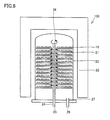
- the CVD apparatus 100 includes a plurality of base material holding jigs 21 for installing the base material 10 and a reaction vessel 22 made of heat resistant alloy steel surrounding the base material holding jig 21. ing.
- a temperature control device 23 for controlling the temperature in the reaction vessel 22 is provided around the reaction vessel 22.
- the gas introduced into the first gas introduction pipe 24 and the gas introduced into the second gas introduction pipe 25 are not mixed.
- a part of the first gas introduction pipe 24 and the second gas introduction pipe 25 is a base installed in the base material holding jig 21 with a gas flowing inside the first gas introduction pipe 24 and the second gas introduction pipe 25, respectively.
- a plurality of through holes for jetting on the material 10 are provided.
- reaction vessel 22 is provided with a gas exhaust pipe 27 for exhausting the gas inside the reaction vessel 22 to the outside.
- the gas inside the reaction vessel 22 passes through the gas exhaust pipe 27 and is discharged from the gas exhaust port 28 to the outside of the reaction vessel 22.
- a method for manufacturing a surface-coated cutting tool using the CVD apparatus 100 will be described.
- a case where a hard layer made of Al, Ti, and N is directly formed on a base material will be described.
- another layer such as a base layer is formed on the base material.
- the hard layer may be formed.
- a surface coating layer can also be formed in order to improve oxidation resistance or the like. Conventionally known methods can be used for forming the underlayer and the surface coating layer.
- a substrate is prepared.
- a commercially available substrate may be used as the substrate, or it may be produced by a general powder metallurgy method.
- a mixed powder can be obtained by mixing WC powder and Co powder with a ball mill or the like. The mixed powder is dried and then molded into a predetermined shape to obtain a molded body. Further, the WC—Co cemented carbide (sintered body) is obtained by sintering the compact.
- a base material made of a WC—Co based cemented carbide can be manufactured by subjecting the sintered body to a predetermined cutting edge processing such as a honing process.
- a predetermined cutting edge processing such as a honing process.
- any conventionally known substrate can be prepared as this type of substrate, even if it is a substrate other than those described above.
- a hard layer is formed on the base material by a CVD method using the CVD apparatus 100. Specifically, first, a chip having an arbitrary shape as the substrate 10 is mounted on the substrate holding jig 21 in the reaction vessel 22 of the CVD apparatus 100. Subsequently, the temperature of the base material 10 installed on the base material holding jig 21 is raised to 750 to 850 ° C. using the temperature control device 23. Further, the pressure inside the reaction vessel 22 is set to 1.5 to 2.5 kPa.
- a first gas group containing TiCl 4 gas and AlCl 3 gas is introduced into the first gas introduction pipe 24 while rotating the gas first gas introduction pipe 24 and the second gas introduction pipe 25 around the shaft 26.
- the second gas group containing NH 3 gas is introduced into the second gas introduction pipe 25.
- the ejected first gas group and second gas group are uniformly mixed in the reaction vessel 22 by a rotating operation, and the mixed gas is directed onto the substrate 10. And the nucleus of the crystal grain containing Al, Ti, and N is produced
- crystal grains are grown while modulating the flow rate of either or both of AlCl 3 gas and TiCl 4 gas.
- a first crystal growth method for modulating the flow rate of TiCl 4 gas, the TiCl 4 gas in the total reaction gas There is a second crystal growth method in which the flow rate of AlCl 3 gas is modulated while maintaining the flow rate constant.
- the atomic ratio of Ti can be controlled by adjusting the flow rate of the TiCl 4 gas (that is, the atomic ratio of Al can also be controlled). Specifically, while maintaining the flow rate of AlCl 3 gas constant at 2 to 3% by volume, the flow rate of TiCl 4 gas is maintained at 3 to 5% by volume (High Flow) for 5 to 30 seconds.
- the first gas group is introduced into the first gas introduction pipe 24.
- TiCl 4 by switching the high and low flow rate of the gas flow rates of TiCl 4 gas 0.2-0.8 vol% (low flow: Low Flow) the first gas group in conditions that maintain 5-30 seconds as a 1
- the gas is introduced into the gas introduction pipe 24. Thereafter, the flow rate of TiCl 4 gas is further switched. By repeating this operation a plurality of times, a hard layer containing crystal grains having a stacked structure in which the first layer and the second layer are alternately stacked can be formed.
- the atomic ratio of Al can be controlled by adjusting the flow rate of the AlCl 3 gas (that is, the atomic ratio of Ti can also be controlled). Specifically, while maintaining the flow rate of TiCl 4 gas constant at 0.5 to 2% by volume, the flow rate of AlCl 3 gas is maintained at 5 to 10% by volume (high flow) for 5 to 10 seconds.
- the first gas group is introduced into the first gas introduction pipe 24 under conditions. Immediately after that, the flow rate of the AlCl 3 gas is immediately switched and the flow rate of the AlCl 3 gas is maintained at 1 to 3% by volume (low flow rate: Low Flow) for 5 to 10 seconds. 24. Thereafter, the flow rate of the AlCl 3 gas is further switched. By repeating this operation a plurality of times, a hard layer containing crystal grains having a stacked structure in which the first layer and the second layer are alternately stacked can be formed.
- a high flow rate (High Flow) in TiCl 4 times for jetting gas or AlCl 3 gas, low flow (Low Flow) at the time of ejecting a TiCl 4 gas or AlCl 3 gas By adjusting the number of times of switching the flow rate of TiCl 4 gas or AlCl 3 gas from a high flow rate to a low flow rate or from a low flow rate to a high flow rate, the thicknesses of the first layer and the second layer, the adjacent first layer and The total thickness with the second layer and the thickness of the hard layer can each be controlled to a desired thickness.
- the orientation of crystal grains contained in the hard layer can be controlled so as to satisfy the above area ratio.
- the length of the ⁇ 3 type crystal grain boundary can be made less than 50% of the length of the ⁇ 3-29 type crystal grain boundary by controlling the volume% of NH 3 that is the raw material gas for the chemical reaction.
- the first gas group preferably contains hydrogen chloride (HCl) gas and hydrogen (H 2 ) gas as a carrier gas, together with TiCl 4 and AlCl 3 gas.
- the second gas group preferably contains argon gas together with NH 3 gas.
- nitrogen (N 2 ) gas may be included.
- nitrogen (N 2 ) gas is not included, and only ammonia (NH 3 ) gas and argon gas are used.
- the second gas group is preferably configured.
- the hard layer can be formed, and the surface-coated cutting tool according to this embodiment can be manufactured.
- the measurement target surface based on the cross section parallel to the normal direction of the surface of the substrate was produced as follows. First, a cross section parallel to the normal direction of the surface of the substrate was prepared. Next, the cross section was polished with water-resistant abrasive paper as described above, and further smoothed by ion milling with Ar ions, which was used as a measurement target surface.
- the ion milling apparatus and its processing conditions are as follows.
- Ion milling device “SM-09010”, manufactured by JEOL Ltd. Acceleration voltage: 6 kV Irradiation angle: 0 ° from the normal direction of the substrate surface Irradiation time: 6 hours.
- the measurement target surface based on a surface parallel to the surface of the substrate was produced as follows. First, a new surface obtained by removing the hard layer located in a region from the surface of the hard layer to a depth of 0.5 ⁇ m in the depth direction was produced. Next, this surface was subjected to FIB processing as described above and mirror-finished, and this was used as a measurement target surface.
- the FIB apparatus used for the FIB processing and its conditions are as follows.
- FIB device “JIB-4501”, manufactured by JEOL Ltd. Acceleration voltage: 30 kV Ion: Gallium (Ga) ion Processing range: 20 ⁇ m ⁇ 20 ⁇ m Processing depth: 0.1 to 0.5 ⁇ m (thickness of hard layer to be removed) Irradiation angle: 5 ° Irradiation time: 1 hour.
- the total thickness of the coating, the thickness of each layer such as the hard layer, the presence of the first layer and the second layer in the crystal grains, and the average value (lamination cycle) of the total thickness of the adjacent first layer and second layer are:
- the measurement was performed by observing the surface to be measured using the STEM high-angle scattering dark field method using STEM (“JEM-2100F”, manufactured by JEOL Ltd.).
- the crystal structure of the crystal grains contained in the hard layer was confirmed by an X-ray diffractometer (“SmartLab”, manufactured by Rigaku Corporation).
- the atomic ratio x of Al in the first layer and the atomic ratio y of Al in the second layer are calculated by an EDX apparatus (“SD100GV”, manufactured by JEOL Ltd.) attached to the TEM, and the calculated atomic ratios x and y The maximum value of xy was determined based on the value.
- the FE-SEM Zero-SEM
- the indentation hardness (GPa) of the hard layer by the nanoindentation method was measured using an ultra-fine indentation hardness tester (“ENT-1100a”, manufactured by Elionix).
- the compressive residual stress (GPa) of the hard layer was calculated by the sin 2 ⁇ method using an X-ray stress measuring device (“SmartLab”, manufactured by Rigaku Corporation).
- SmartLab manufactured by Rigaku Corporation
- the physical property coefficient used for the stress measurement is N.K.
- the values reported in Norrby et al., “Surface & Coatings Technology 257 (2014) 102-107)” were used.
- it is preferable to measure the stress by selecting the diffraction peak on the high angle side so that the peaks of the first hard coating layer and the substrate do not overlap as much as possible in consideration of the type of the substrate used.
- a substrate A and a substrate B were prepared. Specifically, raw material powders having the composition (% by mass) shown in Table 1 were uniformly mixed. “Remaining” in Table 1 indicates that WC occupies the remainder of the composition (mass%).
- the mixed powder is pressed into a predetermined shape and then sintered at 1300 to 1500 ° C. for 1 to 2 hours, whereby a base material A (shape: CNMG120408NUX) and a base material B (made of cemented carbide) Shape: SEET13T3AGSN-G) was obtained.
- the base layer (TiN and TiN and TiCN depending on the sample) of the composition shown in Table 2 was formed on the surface of the base material A and the base material B with the thickness as shown in Table 9.
- a hard layer which will be described later, was formed on the underlayer with a thickness as shown in Table 9.
- a surface coating layer (Al 2 O 3 ) was also formed depending on the sample.
- the underlayer is a layer that is in direct contact with the surface of the substrate.
- a surface coating layer is a layer formed on a hard layer, and comprises the surface of a cutting tool.
- reaction gas composition volume%
- pressure kPa
- temperature ° C.
- reaction atmosphere a condition of the total gas flow rate
- TiN layer the substrate was placed in a reaction vessel of a known CVD apparatus comprising a CVD apparatus 100 shown in FIG. 6, 2.0 vol% of TiCl 4 gas into the reaction vessel, 39. It can be formed by injecting a mixed gas composed of 7% by volume of N 2 gas and the balance H 2 gas at a total gas flow rate of 44.7 L / min in an atmosphere having a pressure of 6.7 kPa and a temperature of 915 ° C. . The thickness of each layer can be controlled by the time during which the reaction gas is ejected.
- the hard layer was formed by using a CVD apparatus 100 as shown in FIG. 6 under any one of the formation conditions 1A to 1H, 2A to 2H, X and Y shown in Tables 3 to 5.
- the first crystal growth method is used in which the crystal grains are grown by modulating the flow rate of the TiCl 4 gas while keeping the flow rate of the AlCl 3 gas constant.
- the formation conditions 2A to 2G used the second crystal growth method in which the crystal grains are grown by modulating the flow rate of the AlCl 3 gas while keeping the flow rate of the TiCl 4 gas constant.
- crystal grains were grown by intermittently supplying the first gas group and the second gas group while keeping the flow rates of the AlCl 3 gas and the TiCl 4 gas constant without modulation. Specifically, the first gas group and the second gas group were supplied at a cycle of stopping for 0.8 seconds and ejecting for 0.2 seconds.
- the formation condition Y the flow rate of the AlCl 3 gas and the TiCl 4 gas was kept constant, and the crystal grains were grown by performing continuous gas ejection.
- the formation condition “1A” indicates that the hard layer is formed under the following conditions. That is, the film forming temperature (base material temperature) is 800 ° C., the pressure in the reaction vessel is 1.5 kPa, and the total gas flow rate that is the sum of the flow rates of the first gas group and the second gas group is 55.0 L / min. To do. Under this condition, the flow rate of the AlCl 3 gas was kept constant at 2.5% by volume, while the TiCl 4 gas was maintained at 0.25% by volume (Low Flow) for 5 seconds (Time). The gas group is introduced into the first gas introduction pipe 24.
- the first gas group is introduced into the first gas introduction pipe 24 under the conditions to be satisfied. Thereafter, the flow rate of the TiCl 4 gas is further switched, and such an operation is performed a plurality of times as desired.
- the TiCl 4 gas is introduced into the first gas introduction pipe 24 at intervals of 5 seconds per minute, 6 times (Interval) each at a high flow rate and a low flow rate.
- the first gas group includes a Ti 2 gas and an AlCl 3 gas, C 2 H 4 gas, and H 2 gas as the balance.
- the second gas group includes each predetermined amount (volume%) of NH 3 gas and Ar gas.
- the flow rate of TiCl 4 or AlCl 3 was modulated in the same manner as “1A”, and a hard layer was formed under the conditions shown in Table 3 or Table 4.
- the hard layer was formed under the conditions shown in Table 5.
- ethylene gas is contained in the first gas group in the volume% as shown in Tables 3 and 4, so that the AlTi carbonitride
- the crystal grains having the laminated structure of the first layer and the second layer made of were grown.
- crystal grains having a laminated structure of a first layer and a second layer made of an AlTi nitride grew.
- the hard layer formed under each of the above conditions is formed by growing crystal grains having a stacked structure in which the first layer and the second layer are alternately stacked at the stacking cycle as shown in Tables 6 to 8. .
- Tables 6 to 8 the thickness of the first layer, the thickness of the second layer, the atomic ratio x (maximum value) of Al in the first layer, and the atomic ratio y (minimum value) of Al in the second layer formed according to each condition.
- the hard layer 2 also shows the area ratio of crystal grains in which the crossing angle of the crystal grains included is 0-10 °, and the area ratio of crystal grains in which the grain size is 0.5 ⁇ m or less.
- All of the crystal grains contained in the hard layer formed under the formation conditions 1A to 1G and 2A to 2G had a sodium chloride type crystal structure. All the crystal grains contained in the hard layer formed under the forming conditions X and Y also had a sodium chloride type crystal structure.
- ⁇ Making cutting tools The base material A or base material B prepared as described above was covered with the film formed by the method as described above, and sample Nos. As shown in Table 9 were used. 1 to 32 cutting tools were produced. In this example, sample No. Cutting tools 1 to 28 are examples, and sample Nos. 29 to 32 cutting tools are comparative examples.
- any of the base material, the base layer, and the hard layer is different for each sample.
- Table 9 when two compounds (for example, “TiN (0.5) -TiCN (2.5)”) are listed in one column, the left side (“TiN (0.5)”) It means that the compound is a layer located on the side close to the surface of the substrate, and the right side (“TiCN (2.5)”) compound is a layer located on the side far from the surface of the substrate.
- the numbers in parentheses mean the thickness of each layer.
- the column indicated by “ ⁇ ” in Table 9 means that no layer is present.
- sample no The values of indentation hardness and compressive residual stress of the hard layer in the cutting tools 1 to 36 are also shown.
- the surface coating layer Al 2 O 3 layer
- Sample No. The thickness of the entire coating of 1 cutting tool is 8.6 ⁇ m.
- the indentation hardness (GPa) exhibited by the hard layer in the cutting tool 1 is 38.5, and the compressive residual stress (GPa) is 2.0.
- Sample No. The cutting tools 1 to 7 and 15 to 21 have sample Nos. Compared to 29 and 30 cutting tools, it was confirmed to have a long life. In particular, sample no. It was confirmed that the cutting tools 20 and 30 were inferior in performance to high-speed cutting because chipping was confirmed.
- sample no. The cutting tools of Nos. 8 to 14 and 22 to 28 are sample Nos. It was confirmed that it has a long life compared with the cutting tools of 31 and 32. In particular, sample no. The cutting tool No. 31 was confirmed to be chipped. It was confirmed that 32 cutting tools were inferior in chipping resistance (chip resistance).
Abstract
Description
特許文献1では、複合窒化物層または複合炭窒化物層が立方晶構造を有し、TiおよびAlの組成が基体の法線方向に沿って周期的に変化することにより、高硬度かつ靱性にも優れる硬質被覆層を実現したとされている。しかしながら、この硬質被覆層は特に耐チッピング性の獲得において改善の余地があった。したがって、未だ高い耐摩耗性と高い耐チッピング性との両特性を有することによって要求される長寿命を実現することには至っておらず、その開発が切望されている。 [Problems to be solved by the present disclosure]
In
[本開示の効果]
上記によれば、高い耐チッピング性を示しつつ、特に高い耐摩耗性を示す表面被覆切削工具を提供することができる。 The present invention has been made in view of the above circumstances, and an object thereof is to provide a surface-coated cutting tool that exhibits particularly high wear resistance while exhibiting high chipping resistance, and a method for manufacturing the same.
[Effects of the present disclosure]
According to the above, it is possible to provide a surface-coated cutting tool that exhibits particularly high wear resistance while exhibiting high chipping resistance.
最初に本発明の実施態様を列記して説明する。 [Description of Embodiment of the Present Invention]
First, embodiments of the present invention will be listed and described.
以下、実施形態について説明する。以下の実施形態の説明に用いられる図面において、同一の参照符号は、同一部分または相当部分を表わす。 [Details of the embodiment of the present invention]
Hereinafter, embodiments will be described. In the drawings used to describe the following embodiments, the same reference numerals represent the same or corresponding parts.
本実施形態に係る表面被覆切削工具は、基材と、該基材上に形成された被膜とを備える。被膜は、基材の全面を被覆することが好ましい。しかしながら、基材の一部がこの被膜で被覆されていなかったり被膜の構成が部分的に異なっていたりしていたとしても、本発明の範囲を逸脱するものではない。 ≪Surface coated cutting tool≫
The surface-coated cutting tool according to this embodiment includes a base material and a film formed on the base material. The coating preferably covers the entire surface of the substrate. However, even if a part of the substrate is not coated with this coating or the configuration of the coating is partially different, it does not depart from the scope of the present invention.
基材は、この種の基材として従来公知のものであればいずれも使用することができる。たとえば、超硬合金(たとえば、WC基超硬合金、WCのほか、Coを含み、あるいはTi、Ta、Nbなどの炭窒化物を添加したものも含む)、サーメット(TiC、TiN、TiCNなどを主成分とするもの)、高速度鋼、セラミックス(炭化チタン、炭化ケイ素、窒化ケイ素、窒化アルミニウム、酸化アルミニウムなど)、立方晶型窒化ホウ素焼結体、またはダイヤモンド焼結体のいずれかであることが好ましい。 ≪Base material≫
Any substrate can be used as long as it is conventionally known as this type of substrate. For example, cemented carbide (for example, WC-based cemented carbide, including WC, including Co or containing carbonitride such as Ti, Ta, Nb), cermet (TiC, TiN, TiCN, etc.) Main component), high-speed steel, ceramics (titanium carbide, silicon carbide, silicon nitride, aluminum nitride, aluminum oxide, etc.), cubic boron nitride sintered body, or diamond sintered body Is preferred.
本実施形態において被膜は、硬質層を含む。この硬質層は、当該被膜中に1層または2層以上含まれることができる。また硬質層以外の他の層を含んでもよいことはいうまでもない。 ≪Coating≫
In the present embodiment, the coating includes a hard layer. This hard layer may be included in the coating in one layer or two or more layers. It goes without saying that layers other than the hard layer may be included.
(結晶粒の結晶構造)
硬質層は、塩化ナトリウム型の結晶構造を有する複数の結晶粒を含む。硬質層に含まれる結晶粒が塩化ナトリウム型の結晶構造を有していることは、X線回折装置、SEM-EBSD装置、TEM分析装置などを用いて確認することができる。 <Hard layer>
(Crystal crystal structure)
The hard layer includes a plurality of crystal grains having a sodium chloride type crystal structure. It can be confirmed that the crystal grains contained in the hard layer have a sodium chloride type crystal structure using an X-ray diffractometer, a SEM-EBSD device, a TEM analyzer, or the like.
硬質層に含まれる結晶粒は、AlxTi1-xの窒化物または炭窒化物からなる第1層と、AlyTi1-yの窒化物または炭窒化物(ただし、x≠y)からなる第2層とが交互に1層以上積層された積層構造を有している。第1層および第2層の組成は、窒化物または炭窒化物のいずれでもよい。ただし、第1層の組成が窒化物となる場合、第2層の組成も窒化物となる。第1層の組成が炭窒化物となる場合、第2層の組成も炭窒化物となる。 (Laminated structure of crystal grains)
The crystal grains contained in the hard layer are composed of a first layer made of nitride or carbonitride of Al x Ti 1-x and a nitride or carbonitride of Al y Ti 1-y (where x ≠ y). The second layer is a laminated structure in which one or more layers are alternately laminated. The composition of the first layer and the second layer may be either nitride or carbonitride. However, when the composition of the first layer is nitride, the composition of the second layer is also nitride. When the composition of the first layer is carbonitride, the composition of the second layer is also carbonitride.
本実施形態において、隣り合う第1層と第2層との厚みの合計(以下、「積層周期」とも称する)は、3~40nmである。このような厚みで第1層と第2層とからなる積層構造を有することにより、結晶粒は高硬度となり、かつ靱性が向上する。この厚みが40nmを超えると、結晶粒がウルツ鉱型結晶構造へ相転移することにより硬度が低下する傾向があり、耐摩耗性に悪影響が及ぶ。隣り合う第1層と第2層との厚みの合計は、好ましくは7~38nmである。 (Total thickness of adjacent first and second layers)
In the present embodiment, the total thickness (hereinafter also referred to as “lamination period”) of the adjacent first layer and second layer is 3 to 40 nm. By having a laminated structure including the first layer and the second layer with such a thickness, the crystal grains have high hardness and toughness is improved. When this thickness exceeds 40 nm, the crystal grains tend to undergo a phase transition to a wurtzite crystal structure, whereby the hardness tends to decrease, and the wear resistance is adversely affected. The total thickness of the adjacent first layer and second layer is preferably 7 to 38 nm.
硬質層において、硬質層のうち基材の表面に平行な面に対し、電子線後方散乱回折(EBSD:Electron Back Scatter Diffraction)装置を用いて複数の結晶粒の結晶方位をそれぞれ解析することにより、結晶粒の結晶面である(111)面に対する法線方向と基材の表面に対する法線方向との交差角を測定した場合に、交差角が0度以上10度未満となる結晶粒の面積比率が40%以上である。硬質層がこれを満たす場合に、硬質層は硬度に特に優れることとなり、もって表面被覆切削工具の優れた耐摩耗性に寄与することができる。上記面積比率の上限値は特に限定されず、硬度の向上の観点からは100%が好ましい。 (Orientation of crystal grains)
In the hard layer, by analyzing the crystal orientation of each of the plurality of crystal grains using a backscatter diffraction (EBSD) device with respect to the surface of the hard layer parallel to the surface of the base material, Area ratio of crystal grains in which the crossing angle is 0 degree or more and less than 10 degrees when the crossing angle between the normal direction to the (111) plane which is the crystal plane of the crystal grain and the normal direction to the surface of the substrate is measured Is 40% or more. When the hard layer satisfies this, the hard layer is particularly excellent in hardness, and thus can contribute to the excellent wear resistance of the surface-coated cutting tool. The upper limit of the area ratio is not particularly limited, and is preferably 100% from the viewpoint of improving hardness.
グループ2:交差角が5度以上10度未満
グループ3:交差角が10度以上15度未満
グループ4:交差角が15度以上20度未満
グループ5:交差角が20度以上25度未満
グループ6:交差角が25度以上30度未満
グループ7:交差角が30度以上35度未満
グループ8:交差角が35度以上40度未満
グループ9:交差角が40度以上45度未満
グループ10:交差角が45度以上50度未満
グループ11:交差角が50度以上55度未満
グループ12:交差角が55度以上60度未満
グループ13:交差角が60度以上65度未満
グループ14:交差角が65度以上70度未満
グループ15:交差角が70度以上75度未満
グループ16:交差角が75度以上80度未満
グループ17:交差角が80度以上85度未満
グループ18:交差角が85度以上90度未満。 Group 1: Crossing angle is 0 degree or more and less than 5 degree Group 2: Crossing angle is 5 degree or more and less than 10 degree Group 3: Crossing angle is 10 degree or more and less than 15 degree Group 4: Crossing angle is 15 degree or more and less than 20 degree Group 5 : Crossing angle between 20 and 25 degrees Group 6: Crossing angle between 25 and 30 degrees Group 7: Crossing angle between 30 and 35 degrees Group 8: Crossing angle between 35 and 40 degrees Group 9:
硬質層に含まれる複数の結晶粒間には、結晶粒の粒界である「結晶粒界」が存在する。特に、硬質層に含まれる結晶粒の結晶粒界は、CSL粒界(対応格子結晶粒界)と一般粒界とを含み、CSL粒界のうちΣ3型結晶粒界の長さは、CSL粒界を構成するΣ3型結晶粒界、Σ5型結晶粒界、Σ7型結晶粒界、Σ9型結晶粒界、Σ11型結晶粒界、Σ13型結晶粒界、Σ15型結晶粒界、Σ17型結晶粒界、Σ19型結晶粒界、Σ21型結晶粒界、Σ23型結晶粒界、Σ25型結晶粒界、Σ27型結晶粒界およびΣ29型結晶粒界のそれぞれの長さの総計であるΣ3-29型結晶粒界の長さの50%未満であることが好ましい。 (Grain boundaries of crystal grains)
Between the plurality of crystal grains included in the hard layer, there is a “crystal grain boundary” that is a grain boundary of the crystal grains. In particular, the grain boundaries of the crystal grains included in the hard layer include CSL grain boundaries (corresponding lattice crystal grain boundaries) and general grain boundaries, and the length of the Σ3-type grain boundary among the CSL grain boundaries is CSL grain boundaries. Σ3-type grain boundary, Σ5-type grain boundary, Σ7-type grain boundary, Σ9-type grain boundary, Σ11-type grain boundary, Σ13-type grain boundary, Σ15-type grain boundary, Σ17-type grain Σ3-29 type, which is the total length of each of the boundary, Σ19-type grain boundary, Σ21-type grain boundary, Σ23-type grain boundary, Σ25-type grain boundary, Σ27-type grain boundary, and Σ29-type grain boundary It is preferably less than 50% of the length of the crystal grain boundary.
硬質層に含まれる結晶粒は、1μm以下の粒径を有することが好ましい。これにより、硬質層の硬度をさらに向上させることができる。硬質層の結晶粒の粒径は、上述の交差角の度数分布の算出方法を利用して、求めることができる。 (Grain size of crystal grains)
The crystal grains contained in the hard layer preferably have a grain size of 1 μm or less. Thereby, the hardness of a hard layer can further be improved. The grain size of the hard layer crystal grains can be determined using the above-described method of calculating the frequency distribution of the crossing angles.
本実施形態において硬質層に含まれる結晶粒は、平均アスペクト比Aが2以上であることが好ましい。本実施形態では、個々の結晶粒において結晶の成長方向に垂直な方向となる幅のうち最大のものを粒子幅wとし、この粒子幅wに対して垂直な方向となる長さのうち最大のものを粒子長さlとし、wとlとの比(l/w)を個々の結晶粒のアスペクト比αとする。さらに、個々の結晶粒について求めたアスペクト比αの平均値を平均アスペクト比A、個々の結晶粒について求めた粒子幅wの平均値を平均粒子幅Wとする。このとき、硬質層に含まれる結晶粒は、平均アスペクト比Aが2以上であり、かつ平均粒子幅Wが0.5μm以下であることがより好ましい。 (Aspect ratio of crystal grains)
In the present embodiment, the crystal grains contained in the hard layer preferably have an average aspect ratio A of 2 or more. In the present embodiment, the maximum width among the widths of the individual crystal grains that are perpendicular to the crystal growth direction is defined as the particle width w, and the maximum of the lengths that are perpendicular to the grain width w. The grain length is 1 and the ratio of l to w (l / w) is the aspect ratio α of each crystal grain. Further, an average value of the aspect ratio α obtained for each crystal grain is an average aspect ratio A, and an average value of the particle width w obtained for each crystal grain is an average grain width W. At this time, it is more preferable that the crystal grains contained in the hard layer have an average aspect ratio A of 2 or more and an average particle width W of 0.5 μm or less.
硬質層は、ナノインデンテーション法による押し込み硬さが30~40GPaであることが好ましい。より好ましくは、32~38GPaである。硬質層のナノインデンテーション法による押し込み硬さが上記範囲であることにより、本実施形態に係る表面被覆切削工具は、耐摩耗性が向上する。特に、耐熱合金などの難削材の切削加工を行う際に優れた性能を発揮することができる。 (Indentation hardness)
The hard layer preferably has an indentation hardness of 30 to 40 GPa by a nanoindentation method. More preferably, it is 32-38 GPa. When the indentation hardness of the hard layer by the nanoindentation method is in the above range, the surface-coated cutting tool according to this embodiment has improved wear resistance. In particular, excellent performance can be achieved when cutting difficult-to-cut materials such as heat-resistant alloys.
硬質層は、圧縮残留応力を有することが好ましく、該残留応力は、その絶対値が0.5GPa以上3.0GPa以下であることが好ましい。すなわち硬質層が圧縮残留応力を有する場合、その絶対値は3.0GPa以下であることが好ましい。硬質層の圧縮残留応力の絶対値が上記範囲であることにより、硬質層の靱性を飛躍的に向上させることができる。一方、圧縮残留応力の絶対値が3.0GPaを超えると、組織破壊に伴い耐摩耗性が低下する傾向がある。また圧縮残留応力の絶対値が0.5GPa下回ると、チッピングが起きやすくなる傾向がある。靱性が低下する傾向がある。硬質層の圧縮残留応力は、硬質層に含まれる結晶粒内における第1層と第2層との積層周期を調節することによって制御することができる。 (Compressive residual stress)
The hard layer preferably has a compressive residual stress, and the residual stress preferably has an absolute value of 0.5 GPa to 3.0 GPa. That is, when the hard layer has compressive residual stress, the absolute value is preferably 3.0 GPa or less. When the absolute value of the compressive residual stress of the hard layer is in the above range, the toughness of the hard layer can be dramatically improved. On the other hand, if the absolute value of the compressive residual stress exceeds 3.0 GPa, the wear resistance tends to decrease with the destruction of the structure. If the absolute value of the compressive residual stress is less than 0.5 GPa, chipping tends to occur. Toughness tends to decrease. The compressive residual stress of the hard layer can be controlled by adjusting the lamination period of the first layer and the second layer in the crystal grains included in the hard layer.
硬質層は、1~15μmの厚みを有することが好ましい。硬質層の厚みが上記範囲であることにより、高い耐チッピング性を示しつつ、特に高い耐摩耗性を示す効果を顕著に示すことができる。硬質層の厚みが1μm未満であると靱性が十分ではなく、15μmを超えるとチッピングが起きやすくなる傾向がある。硬質層の厚みは、その特性を向上させる観点から3.5~7.0μmであることがさらに好ましい。 (Hard layer thickness)
The hard layer preferably has a thickness of 1 to 15 μm. When the thickness of the hard layer is in the above range, the effect of exhibiting particularly high wear resistance can be remarkably exhibited while exhibiting high chipping resistance. If the thickness of the hard layer is less than 1 μm, the toughness is not sufficient, and if it exceeds 15 μm, chipping tends to occur. The thickness of the hard layer is more preferably 3.5 to 7.0 μm from the viewpoint of improving the characteristics.
硬質層は、本実施形態の作用効果に影響を及ぼさない限り、塩素(Cl)、酸素(O)、硼素(B)、コバルト(Co)、タングステン(W)、クロム(Cr)、タンタル(Ta)、ニオブ(Nb)、炭素(C)などを含んでいてもよい。すなわち硬質層は、不可避不純物などの不純物を含んで形成されることが許容される。 (impurities)
As long as the hard layer does not affect the function and effect of this embodiment, chlorine (Cl), oxygen (O), boron (B), cobalt (Co), tungsten (W), chromium (Cr), tantalum (Ta) ), Niobium (Nb), carbon (C), and the like. That is, the hard layer is allowed to be formed including impurities such as inevitable impurities.
本実施形態において被膜は、硬質層以外の層を含んでいてもよい。たとえば、基材と被膜との接合強度を高くすることが可能な下地層を含むことができる。そのような層として、たとえば、TiN層、TiCN層、TiN層とTiCN層とからなる複合層などを挙げることができる。下地層は、従来公知の製造方法を使用することにより製造することができる。 <Other layers>
In the present embodiment, the coating film may include a layer other than the hard layer. For example, the base layer which can make the joining strength of a base material and a film high can be included. Examples of such a layer include a TiN layer, a TiCN layer, a composite layer composed of a TiN layer and a TiCN layer, and the like. The underlayer can be produced by using a conventionally known production method.
本実施形態に係る表面被覆切削工具は、たとえば、鋳鉄の連続切削、特に乾式のフライス加工などに用いた場合であっても、チッピング、欠損、剥離などの発生が抑えられつつ、極めて高い硬度に基づく高い耐摩耗性を発揮する。したがって、本実施形態に係る表面被覆切削工具は、高い耐チッピング性を示しつつ、特に高い耐摩耗性を示すことができ、もって長寿命を実現することができる。 <Effect>
The surface-coated cutting tool according to the present embodiment has an extremely high hardness while suppressing occurrence of chipping, chipping, peeling, and the like even when used for, for example, continuous cutting of cast iron, particularly dry milling. High wear resistance based. Therefore, the surface-coated cutting tool according to this embodiment can exhibit particularly high wear resistance while exhibiting high chipping resistance, and thus can achieve a long life.
本実施形態に係る表面被覆切削工具の製造方法は、基材を準備する第1工程と、硬質層をCVD法を用いて形成する第2工程とを含む。特に、第2工程は、AlCl3ガスおよびTiCl4ガスの両方またはいずれか一方の流量を変調させる工程を含む。これにより、上記の構成および効果を有する表面被覆切削工具を製造することができる。 ≪Method for manufacturing surface-coated cutting tool≫
The manufacturing method of the surface coating cutting tool which concerns on this embodiment includes the 1st process of preparing a base material, and the 2nd process of forming a hard layer using CVD method. In particular, the second step includes a step of modulating the flow rate of AlCl 3 gas and / or TiCl 4 gas. Thereby, the surface coating cutting tool which has said structure and effect can be manufactured.
第1工程では基材を準備する。基材は、市販のものを用いてもよく、一般的な粉末冶金法で製造してもよい。たとえば、基材として超硬合金基材を一般的な粉末冶金法で製造する場合、ボールミルなどによってWC粉末とCo粉末などとを混合して混合粉末を得ることができる。該混合粉末を乾燥した後、所定の形状に成形して成形体を得る。さらに該成形体を焼結することにより、WC-Co系超硬合金(焼結体)を得る。次いで該焼結体に対して、ホーニング処理などの所定の刃先加工を施すことにより、WC-Co系超硬合金からなる基材を製造することができる。第1工程では、上記以外の基材であっても、この種の基材として従来公知のものをいずれも準備可能である。 <First step>
In the first step, a substrate is prepared. A commercially available substrate may be used as the substrate, or it may be produced by a general powder metallurgy method. For example, when a cemented carbide substrate is manufactured as a substrate by a general powder metallurgy method, a mixed powder can be obtained by mixing WC powder and Co powder with a ball mill or the like. The mixed powder is dried and then molded into a predetermined shape to obtain a molded body. Further, the WC—Co cemented carbide (sintered body) is obtained by sintering the compact. Next, a base material made of a WC—Co based cemented carbide can be manufactured by subjecting the sintered body to a predetermined cutting edge processing such as a honing process. In the first step, any conventionally known substrate can be prepared as this type of substrate, even if it is a substrate other than those described above.
第2工程では、CVD装置100を用いたCVD法により、基材上に硬質層を形成する。具体的には、まずCVD装置100の反応容器22内に、基材10として任意の形状のチップを基材保持治具21に装着する。続いて調温装置23を使って基材保持治具21に設置した基材10の温度を750~850℃に上昇させる。さらに反応容器22の内部の圧力を1.5~2.5kPaとする。 <Second step>
In the second step, a hard layer is formed on the base material by a CVD method using the
基材の表面の法線方向に平行な断面に基づく測定対象面は、次のようにして作製された。まず、基材の表面の法線方向に平行な断面を作製した。次に、該断面を上述のとおり耐水研磨紙で研磨し、引続き、Arイオンによるイオンミーリング処理によりさらに平滑化し、これを測定対象面とした。イオンミーリング装置とその処理の条件は以下のとおりである。 ≪Measurement method≫
The measurement target surface based on the cross section parallel to the normal direction of the surface of the substrate was produced as follows. First, a cross section parallel to the normal direction of the surface of the substrate was prepared. Next, the cross section was polished with water-resistant abrasive paper as described above, and further smoothed by ion milling with Ar ions, which was used as a measurement target surface. The ion milling apparatus and its processing conditions are as follows.
加速電圧:6kV
照射角度:基材表面の法線方向から0°
照射時間:6時間。 Ion milling device: “SM-09010”, manufactured by JEOL Ltd. Acceleration voltage: 6 kV
Irradiation angle: 0 ° from the normal direction of the substrate surface
Irradiation time: 6 hours.
加速電圧:30kV
イオン :ガリウム(Ga)イオン
加工範囲:20μm×20μm
加工深さ:0.1~0.5μm(除去される硬質層の厚さ)
照射角度:5°
照射時間:1時間。 FIB device: “JIB-4501”, manufactured by JEOL Ltd. Acceleration voltage: 30 kV
Ion: Gallium (Ga) ion Processing range: 20 μm × 20 μm
Processing depth: 0.1 to 0.5 μm (thickness of hard layer to be removed)
Irradiation angle: 5 °
Irradiation time: 1 hour.
第1工程として、基材Aおよび基材Bを準備した。具体的には、表1に記載の配合組成(質量%)からなる原料粉末を均一に混合した。なお表1中の「残り」とは、WCが配合組成(質量%)の残部を占めることを示す。次に、この混合粉末を所定の形状に加圧成形した後に、1300~1500℃で1~2時間焼結することにより、超硬合金からなる基材A(形状:CNMG120408NUX)および基材B(形状:SEET13T3AGSN-G)を得た。これらの形状は、いずれも住友電工ハードメタル株式会社製のものであり、基材AであるCNMG120408NUXは、旋削用の刃先交換型切削チップの形状であり、基材BであるSEET13T3AGSN-Gは、転削(フライス)用の刃先交換型切削チップの形状である。 ≪Preparation of base material≫
As a first step, a substrate A and a substrate B were prepared. Specifically, raw material powders having the composition (% by mass) shown in Table 1 were uniformly mixed. “Remaining” in Table 1 indicates that WC occupies the remainder of the composition (mass%). Next, the mixed powder is pressed into a predetermined shape and then sintered at 1300 to 1500 ° C. for 1 to 2 hours, whereby a base material A (shape: CNMG120408NUX) and a base material B (made of cemented carbide) Shape: SEET13T3AGSN-G) was obtained. These shapes are all manufactured by Sumitomo Electric Hardmetal Co., Ltd., CNMG120408NUX, which is the base material A, is the shape of a cutting edge exchangeable cutting tip for turning, and the SEET13T3AGSN-G, which is the base material B, is This is the shape of a cutting edge-exchangeable cutting tip for milling.

第2工程として、基材Aおよび基材Bの表面上に表2に示す組成の下地層(TiN、試料によってはTiNおよびTiCN)を、表9に示すとおりの厚みで形成した。下地層上に後述する硬質層を表9に示すとおりの厚みで形成した。そのほか表9に示すとおり、試料によっては表面被覆層(Al2O3)も形成した。下地層は基材の表面と直接接する層である。表面被覆層は、硬質層上に形成される層であって切削工具の表面を構成する。 ≪Formation of film≫
As a 2nd process, the base layer (TiN and TiN and TiCN depending on the sample) of the composition shown in Table 2 was formed on the surface of the base material A and the base material B with the thickness as shown in Table 9. A hard layer, which will be described later, was formed on the underlayer with a thickness as shown in Table 9. In addition, as shown in Table 9, a surface coating layer (Al 2 O 3 ) was also formed depending on the sample. The underlayer is a layer that is in direct contact with the surface of the substrate. A surface coating layer is a layer formed on a hard layer, and comprises the surface of a cutting tool.

硬質層の形成は、図6に示すようなCVD装置100を用い、表3~表5に示す形成条件1A~1H、2A~2H、XおよびYのいずれかの条件で行なった。 <Formation of hard layer>
The hard layer was formed by using a
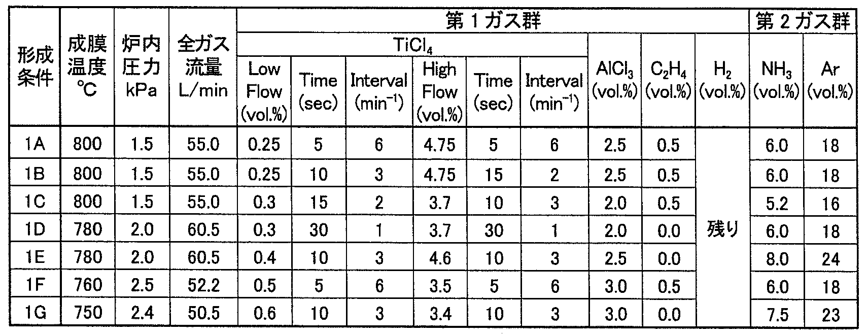


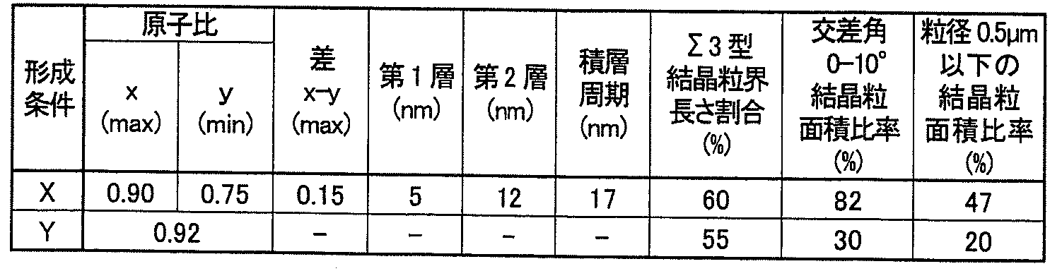
上述のように準備された基材Aまたは基材Bを、上記のような方法で形成した被膜により被覆し、表9に示すとおりの試料No.1~32の切削工具を作製した。本実施例において試料No.1~28の切削工具が実施例であり、試料No.29~32の切削工具が比較例である。 ≪Making cutting tools≫
The base material A or base material B prepared as described above was covered with the film formed by the method as described above, and sample Nos. As shown in Table 9 were used. 1 to 32 cutting tools were produced. In this example, sample No.

上記のようにして作製した試料No.1~32の切削工具を用いて、以下の2種の切削試験を行った。 ≪Cutting test≫
Sample No. produced as described above. The following two types of cutting tests were performed using 1 to 32 cutting tools.
試料No.1~7、15~21、29および30の切削工具について、以下の切削条件により逃げ面摩耗量(Vb)が0.20mmとなるまでの切削時間を測定するとともに刃先の最終損傷形態を観察し、工具寿命を評価した。その結果を表10に示す。切削時間が長いほど耐摩耗性に優れる切削工具として、高速切削であっても長寿命化を実現することができる可能性が高いと評価することができる。 <Round bar peripheral high speed cutting test>
Sample No. For cutting tools 1-7, 15-21, 29 and 30, the cutting time until the flank wear amount (Vb) reached 0.20 mm was measured under the following cutting conditions, and the final damage form of the cutting edge was observed. The tool life was evaluated. The results are shown in Table 10. It can be evaluated that a cutting tool that has higher wear resistance as the cutting time is longer is likely to have a longer life even at high speed cutting.
被削材 : FCD600丸棒
周速 : 300m/min
送り速度: 0.15mm/rev
切込み量: 1.0mm
切削液 : 有り。 (Cutting conditions for round bar outer periphery high-speed cutting test)
Work material: FCD600 round bar Peripheral speed: 300m / min
Feeding speed: 0.15mm / rev
Cutting depth: 1.0mm
Cutting fluid: Yes.
試料No.8~14、22~28、31および32の切削工具について、以下の切削条件により逃げ面摩耗量(Vb)が0.20mmとなるまでの切削距離を測定するとともに刃先の最終損傷形態を観察し、工具寿命を評価した。その結果を表11に示す。切削距離が長いほど耐チッピング性に優れる切削工具として、被削材の種類に関わらず長寿命化を実現することができる可能性が高いと評価することができる。 <Block material fracture resistance test>
Sample No. For the cutting tools 8-14, 22-28, 31 and 32, the cutting distance until the flank wear amount (Vb) reached 0.20 mm was measured under the following cutting conditions and the final damage form of the cutting edge was observed. The tool life was evaluated. The results are shown in Table 11. It can be evaluated that the longer the cutting distance, the higher the possibility that a long tool life can be realized regardless of the type of the work material as a cutting tool with excellent chipping resistance.
被削材 : SKDブロック材
周速 : 200m/min
送り速度: 0.3mm/s
切込み量: 2.0mm
切削液 : なし
カッタ : WGC4160R(住友電工ハードメタル株式会社製)。 (Cutting conditions for block material fracture resistance test)
Work material: SKD block material Peripheral speed: 200 m / min
Feeding speed: 0.3mm / s
Cutting depth: 2.0mm
Cutting fluid: None Cutter: WGC4160R (manufactured by Sumitomo Electric Hardmetal Corporation).

表10によれば、試料No.1~7、15~21の切削工具は、試料No.29および30の切削工具と比べて長寿命であることが確認された。特に、試料No.20および30の切削工具は、チッピングが確認されて高速切削に対して性能が劣ることが確認された。 <Evaluation>
According to Table 10, Sample No. The
Claims (7)
- 基材と、該基材上に形成された被膜とを備える表面被覆切削工具であって、
前記被膜は、硬質層を含み、
前記硬質層は、塩化ナトリウム型の結晶構造を有する複数の結晶粒を含み、
前記結晶粒は、AlxTi1-xの窒化物または炭窒化物からなる第1層と、AlyTi1-yの窒化物または炭窒化物(ただしx≠y)からなる第2層とが交互に積層された積層構造を有し、
隣り合う前記第1層と前記第2層との厚みの合計は、3nm以上40nm以下であり、
前記硬質層のうち前記基材の表面に平行な面に対し、電子線後方散乱回折装置を用いて前記複数の結晶粒の結晶方位をそれぞれ解析することにより、前記結晶粒の結晶面である(111)面に対する法線方向と前記基材の表面に対する法線方向との交差角を測定した場合に、前記交差角が0度以上10度未満となる前記結晶粒の面積比率が40%以上である、表面被覆切削工具。 A surface-coated cutting tool comprising a substrate and a coating formed on the substrate,
The coating includes a hard layer,
The hard layer includes a plurality of crystal grains having a sodium chloride type crystal structure;
The crystal grains include a first layer made of an Al x Ti 1-x nitride or carbonitride, and a second layer made of an Al y Ti 1-y nitride or carbonitride (where x ≠ y). Has a laminated structure in which are alternately laminated,
The total thickness of the adjacent first layer and second layer is 3 nm or more and 40 nm or less,
By analyzing the crystal orientation of each of the plurality of crystal grains using an electron beam backscattering diffractometer with respect to a plane parallel to the surface of the substrate of the hard layer, the crystal plane of the crystal grains ( When the crossing angle between the normal direction to the (111) plane and the normal direction to the surface of the substrate is measured, the area ratio of the crystal grains at which the crossing angle is 0 degree or more and less than 10 degrees is 40% or more. There is a surface-coated cutting tool. - 前記結晶粒の粒界は、CSL粒界と、一般粒界とを含み、CSL粒界のうちΣ3型結晶粒界の長さは、CSL粒界を構成するΣ3型結晶粒界、Σ5型結晶粒界、Σ7型結晶粒界、Σ9型結晶粒界、Σ11型結晶粒界、Σ13型結晶粒界、Σ15型結晶粒界、Σ17型結晶粒界、Σ19型結晶粒界、Σ21型結晶粒界、Σ23型結晶粒界、Σ25型結晶粒界、Σ27型結晶粒界およびΣ29型結晶粒界のそれぞれの長さの総計であるΣ3-29型結晶粒界の長さの50%未満である、請求項1に記載の表面被覆切削工具。 The grain boundary of the crystal grain includes a CSL grain boundary and a general grain boundary, and the length of the Σ3 type grain boundary in the CSL grain boundary is a Σ3 type grain boundary or Σ5 type crystal constituting the CSL grain boundary. Grain boundary, Σ7 type grain boundary, Σ9 type grain boundary, Σ11 type grain boundary, Σ13 type grain boundary, Σ15 type grain boundary, Σ17 type grain boundary, Σ19 type grain boundary, Σ21 type grain boundary Less than 50% of the length of the Σ3-29 type grain boundary, which is the total length of each of the Σ23 type crystal grain boundary, Σ25 type crystal grain boundary, Σ27 type crystal grain boundary, and Σ29 type crystal grain boundary, The surface-coated cutting tool according to claim 1.
- 前記結晶粒は1μm以下の粒径を有する、請求項1または請求項2に記載の表面被覆切削工具。 The surface-coated cutting tool according to claim 1 or 2, wherein the crystal grains have a particle size of 1 µm or less.
- 前記硬質層は、1μm以上15μm以下の厚みを有する、請求項1から請求項3のいずれか1項に記載の表面被覆切削工具。 The surface-coated cutting tool according to any one of claims 1 to 3, wherein the hard layer has a thickness of 1 µm to 15 µm.
- 前記硬質層は、ナノインデンテーション法による押し込み硬さが30GPa以上40GPa以下である、請求項1から請求項4のいずれか1項に記載の表面被覆切削工具。 The surface-coated cutting tool according to any one of claims 1 to 4, wherein the hard layer has an indentation hardness of 30 GPa or more and 40 GPa or less by a nanoindentation method.
- 前記硬質層は、圧縮残留応力の絶対値が0.5GPa以上3.0GPa以下である、請求項1から請求項5のいずれか1項に記載の表面被覆切削工具。 The surface-coated cutting tool according to any one of claims 1 to 5, wherein the hard layer has an absolute value of compressive residual stress of 0.5 GPa or more and 3.0 GPa or less.
- 請求項1から請求項6のいずれか1項に記載の表面被覆切削工具の製造方法であって、
前記基材を準備する第1工程と、
前記硬質層を化学蒸着法を用いて形成する第2工程とを含み、
前記第2工程は、AlCl3ガスおよびTiCl4ガスの両方またはいずれか一方の流量を変調させながら前記結晶粒を成長させる工程を含む、表面被覆切削工具の製造方法。 It is a manufacturing method of the surface covering cutting tool according to any one of claims 1 to 6,
A first step of preparing the substrate;
A second step of forming the hard layer using chemical vapor deposition,
The method of manufacturing a surface-coated cutting tool, wherein the second step includes a step of growing the crystal grains while modulating the flow rate of either or both of AlCl 3 gas and TiCl 4 gas.
Priority Applications (4)
| Application Number | Priority Date | Filing Date | Title |
|---|---|---|---|
| US16/091,612 US10953473B2 (en) | 2016-04-14 | 2016-06-22 | Surface-coated cutting tool and method of producing the same |
| EP16898679.2A EP3444053B1 (en) | 2016-04-14 | 2016-06-22 | Surface-coated cutting tool and manufacturing method therefor |
| KR1020187029215A KR102198745B1 (en) | 2016-04-14 | 2016-06-22 | Surface-coated cutting tool and its manufacturing method |
| CN201680084592.7A CN109070234B (en) | 2016-04-14 | 2016-06-22 | Surface-coated cutting tool and method for manufacturing same |
Applications Claiming Priority (2)
| Application Number | Priority Date | Filing Date | Title |
|---|---|---|---|
| JP2016-081095 | 2016-04-14 | ||
| JP2016081095A JP6973699B2 (en) | 2016-04-14 | 2016-04-14 | Surface coating cutting tool and its manufacturing method |
Publications (1)
| Publication Number | Publication Date |
|---|---|
| WO2017179221A1 true WO2017179221A1 (en) | 2017-10-19 |
Family
ID=60042459
Family Applications (1)
| Application Number | Title | Priority Date | Filing Date |
|---|---|---|---|
| PCT/JP2016/068502 WO2017179221A1 (en) | 2016-04-14 | 2016-06-22 | Surface-coated cutting tool and manufacturing method therefor |
Country Status (6)
| Country | Link |
|---|---|
| US (1) | US10953473B2 (en) |
| EP (1) | EP3444053B1 (en) |
| JP (1) | JP6973699B2 (en) |
| KR (1) | KR102198745B1 (en) |
| CN (1) | CN109070234B (en) |
| WO (1) | WO2017179221A1 (en) |
Cited By (3)
| Publication number | Priority date | Publication date | Assignee | Title |
|---|---|---|---|---|
| JP6750789B1 (en) * | 2019-04-17 | 2020-09-02 | 住友電工ハードメタル株式会社 | Cutting tools |
| JP2020142314A (en) * | 2019-03-05 | 2020-09-10 | 三菱マテリアル株式会社 | Surface-coating cutting tool having hard coating layer exerting excellent abrasion resistance and peeling resistance |
| WO2020213259A1 (en) * | 2019-04-17 | 2020-10-22 | 住友電工ハードメタル株式会社 | Cutting tool |
Families Citing this family (13)
| Publication number | Priority date | Publication date | Assignee | Title |
|---|---|---|---|---|
| JP5618429B2 (en) | 2012-12-28 | 2014-11-05 | 住友電工ハードメタル株式会社 | Surface covering member and manufacturing method thereof |
| KR102064172B1 (en) * | 2017-09-01 | 2020-01-09 | 한국야금 주식회사 | Hard film having excellent wear resistance and toughness |
| JP6565091B1 (en) * | 2018-03-22 | 2019-08-28 | 住友電工ハードメタル株式会社 | Surface-coated cutting tool and manufacturing method thereof |
| US11274366B2 (en) * | 2018-03-22 | 2022-03-15 | Sumitomo Electric Hardmetal Corp. | Surface-coated cutting tool and method for manufacturing same |
| US11311945B2 (en) * | 2018-03-22 | 2022-04-26 | Sumitomo Electric Hardmetal Corp. | Surface-coated cutting tool and method for manufacturing same |
| JP6784928B2 (en) * | 2018-09-04 | 2020-11-18 | 株式会社タンガロイ | Cover cutting tool |
| WO2020213260A1 (en) * | 2019-04-17 | 2020-10-22 | 住友電工ハードメタル株式会社 | Cutting tool |
| JP7187397B2 (en) * | 2019-07-18 | 2022-12-12 | オークマ株式会社 | Re-learning Necessity Determining Method and Re-learning Necessity Determining Device for Diagnosis Model in Machine Tool, Re-learning Necessity Determining Program |
| WO2021024736A1 (en) * | 2019-08-06 | 2021-02-11 | 住友電工ハードメタル株式会社 | Cutting tool |
| EP3991891B1 (en) * | 2019-10-10 | 2023-04-26 | Sumitomo Electric Hardmetal Corp. | Cutting tool |
| JP7167966B2 (en) * | 2020-07-08 | 2022-11-09 | 株式会社タンガロイ | coated cutting tools |
| WO2022264196A1 (en) * | 2021-06-14 | 2022-12-22 | 住友電工ハードメタル株式会社 | Cutting tool |
| EP4292736A1 (en) * | 2022-01-25 | 2023-12-20 | Sumitomo Electric Industries, Ltd. | Cutting tool and method for manufacturing same |
Citations (7)
| Publication number | Priority date | Publication date | Assignee | Title |
|---|---|---|---|---|
| JP2007203447A (en) * | 2006-02-06 | 2007-08-16 | Mitsubishi Materials Corp | Surface-coated cermet cutting tool with hard coating layer having excellent chipping resistance in high-speed intermittent cutting work |
| JP2008307615A (en) * | 2007-06-12 | 2008-12-25 | Mitsubishi Materials Corp | Surface-coated cutting tool with hard coating layer exerting excellent chipping resistance in heavy cutting work and its manufacturing method |
| JP2015163423A (en) * | 2014-01-31 | 2015-09-10 | 三菱マテリアル株式会社 | Surface coated cutting tool whose hard coating layer exerts excellent chipping resistance in high-speed intermittent cutting work |
| JP2016003369A (en) * | 2014-06-17 | 2016-01-12 | 住友電工ハードメタル株式会社 | Hard coating, cutting tool and method for manufacturing hard coating |
| US20160053372A1 (en) * | 2013-04-26 | 2016-02-25 | Walter Ag | Tool having CVD coating |
| EP3000913A1 (en) * | 2014-09-26 | 2016-03-30 | Walter Ag | Coated cutting tool insert with MT-CVD TiCN on TiAI(C,N) |
| WO2016047581A1 (en) * | 2014-09-25 | 2016-03-31 | 三菱マテリアル株式会社 | Surface-coated cutting tool in which hard coating layer exhibits excellent chipping resistance |
Family Cites Families (6)
| Publication number | Priority date | Publication date | Assignee | Title |
|---|---|---|---|---|
| ES2157383T3 (en) * | 1996-07-18 | 2001-08-16 | Mitsubishi Materials Corp | TITANIUM CARBONITRIDE CERAMETAL CUTTING SHEET AND COVERED CERAMETAL CUTTING SHEET. |
| DE10002861A1 (en) * | 2000-01-24 | 2001-08-09 | Walter Ag | Cutting tool with carbonitride coating |
| JP5287125B2 (en) * | 2008-10-15 | 2013-09-11 | 三菱マテリアル株式会社 | A surface-coated cutting tool with a hard coating layer that provides excellent fracture resistance and wear resistance |
| FR2972804A1 (en) * | 2011-03-16 | 2012-09-21 | Contralco Sas Soc | Chemical analysis device for chemical analysis of breath of user for detecting presence of alcohol in breath, has cap with lateral wall axially fitted at end of test tube, and shoulder bearing axially against valve that closes thrust member |
| JP5939508B2 (en) * | 2012-07-25 | 2016-06-22 | 三菱マテリアル株式会社 | A surface-coated cutting tool that exhibits excellent chipping resistance with a hard coating layer in high-speed intermittent cutting |
| JP6402662B2 (en) | 2014-03-26 | 2018-10-10 | 三菱マテリアル株式会社 | Surface-coated cutting tool and manufacturing method thereof |
-
2016
- 2016-04-14 JP JP2016081095A patent/JP6973699B2/en active Active
- 2016-06-22 US US16/091,612 patent/US10953473B2/en active Active
- 2016-06-22 KR KR1020187029215A patent/KR102198745B1/en active IP Right Grant
- 2016-06-22 WO PCT/JP2016/068502 patent/WO2017179221A1/en active Application Filing
- 2016-06-22 EP EP16898679.2A patent/EP3444053B1/en active Active
- 2016-06-22 CN CN201680084592.7A patent/CN109070234B/en active Active
Patent Citations (7)
| Publication number | Priority date | Publication date | Assignee | Title |
|---|---|---|---|---|
| JP2007203447A (en) * | 2006-02-06 | 2007-08-16 | Mitsubishi Materials Corp | Surface-coated cermet cutting tool with hard coating layer having excellent chipping resistance in high-speed intermittent cutting work |
| JP2008307615A (en) * | 2007-06-12 | 2008-12-25 | Mitsubishi Materials Corp | Surface-coated cutting tool with hard coating layer exerting excellent chipping resistance in heavy cutting work and its manufacturing method |
| US20160053372A1 (en) * | 2013-04-26 | 2016-02-25 | Walter Ag | Tool having CVD coating |
| JP2015163423A (en) * | 2014-01-31 | 2015-09-10 | 三菱マテリアル株式会社 | Surface coated cutting tool whose hard coating layer exerts excellent chipping resistance in high-speed intermittent cutting work |
| JP2016003369A (en) * | 2014-06-17 | 2016-01-12 | 住友電工ハードメタル株式会社 | Hard coating, cutting tool and method for manufacturing hard coating |
| WO2016047581A1 (en) * | 2014-09-25 | 2016-03-31 | 三菱マテリアル株式会社 | Surface-coated cutting tool in which hard coating layer exhibits excellent chipping resistance |
| EP3000913A1 (en) * | 2014-09-26 | 2016-03-30 | Walter Ag | Coated cutting tool insert with MT-CVD TiCN on TiAI(C,N) |
Non-Patent Citations (1)
| Title |
|---|
| See also references of EP3444053A4 * |
Cited By (5)
| Publication number | Priority date | Publication date | Assignee | Title |
|---|---|---|---|---|
| JP2020142314A (en) * | 2019-03-05 | 2020-09-10 | 三菱マテリアル株式会社 | Surface-coating cutting tool having hard coating layer exerting excellent abrasion resistance and peeling resistance |
| JP7274121B2 (en) | 2019-03-05 | 2023-05-16 | 三菱マテリアル株式会社 | A surface-coated cutting tool with a hard coating layer that exhibits excellent wear resistance and peeling resistance. |
| JP6750789B1 (en) * | 2019-04-17 | 2020-09-02 | 住友電工ハードメタル株式会社 | Cutting tools |
| WO2020213259A1 (en) * | 2019-04-17 | 2020-10-22 | 住友電工ハードメタル株式会社 | Cutting tool |
| US11007580B2 (en) | 2019-04-17 | 2021-05-18 | Sumitomo Electric Hardmetal Corp. | Cutting tool |
Also Published As
| Publication number | Publication date |
|---|---|
| EP3444053B1 (en) | 2023-11-22 |
| KR102198745B1 (en) | 2021-01-05 |
| JP2017189847A (en) | 2017-10-19 |
| EP3444053A4 (en) | 2019-10-09 |
| EP3444053A1 (en) | 2019-02-20 |
| US20190151956A1 (en) | 2019-05-23 |
| JP6973699B2 (en) | 2021-12-01 |
| CN109070234A (en) | 2018-12-21 |
| KR20180123092A (en) | 2018-11-14 |
| CN109070234B (en) | 2021-06-15 |
| US10953473B2 (en) | 2021-03-23 |
Similar Documents
| Publication | Publication Date | Title |
|---|---|---|
| WO2017179221A1 (en) | Surface-coated cutting tool and manufacturing method therefor | |
| JP6037256B1 (en) | Surface-coated cutting tool and manufacturing method thereof | |
| JP6037255B1 (en) | Surface-coated cutting tool and manufacturing method thereof | |
| JP6045010B1 (en) | Surface-coated cutting tool and manufacturing method thereof | |
| JP6044861B1 (en) | Surface-coated cutting tool and manufacturing method thereof | |
| WO2020170572A1 (en) | Cutting tool | |
| US11220760B2 (en) | Surface-coated cutting tool and method of producing the same | |
| JP6750789B1 (en) | Cutting tools |
Legal Events
| Date | Code | Title | Description |
|---|---|---|---|
| ENP | Entry into the national phase |
Ref document number: 20187029215 Country of ref document: KR Kind code of ref document: A |
|
| NENP | Non-entry into the national phase |
Ref country code: DE |
|
| WWE | Wipo information: entry into national phase |
Ref document number: 2016898679 Country of ref document: EP |
|
| ENP | Entry into the national phase |
Ref document number: 2016898679 Country of ref document: EP Effective date: 20181114 |
|
| 121 | Ep: the epo has been informed by wipo that ep was designated in this application |
Ref document number: 16898679 Country of ref document: EP Kind code of ref document: A1 |