WO2017169566A1 - 表示装置、光学素子、及び、電子機器 - Google Patents
表示装置、光学素子、及び、電子機器 Download PDFInfo
- Publication number
- WO2017169566A1 WO2017169566A1 PCT/JP2017/008985 JP2017008985W WO2017169566A1 WO 2017169566 A1 WO2017169566 A1 WO 2017169566A1 JP 2017008985 W JP2017008985 W JP 2017008985W WO 2017169566 A1 WO2017169566 A1 WO 2017169566A1
- Authority
- WO
- WIPO (PCT)
- Prior art keywords
- optical element
- pixels
- resin layer
- display device
- display
- Prior art date
- Legal status (The legal status is an assumption and is not a legal conclusion. Google has not performed a legal analysis and makes no representation as to the accuracy of the status listed.)
- Ceased
Links
Images


Classifications
-
- G—PHYSICS
- G02—OPTICS
- G02B—OPTICAL ELEMENTS, SYSTEMS OR APPARATUS
- G02B30/00—Optical systems or apparatus for producing three-dimensional [3D] effects, e.g. stereoscopic images
- G02B30/20—Optical systems or apparatus for producing three-dimensional [3D] effects, e.g. stereoscopic images by providing first and second parallax images to an observer's left and right eyes
- G02B30/26—Optical systems or apparatus for producing three-dimensional [3D] effects, e.g. stereoscopic images by providing first and second parallax images to an observer's left and right eyes of the autostereoscopic type
- G02B30/27—Optical systems or apparatus for producing three-dimensional [3D] effects, e.g. stereoscopic images by providing first and second parallax images to an observer's left and right eyes of the autostereoscopic type involving lenticular arrays
- G02B30/29—Optical systems or apparatus for producing three-dimensional [3D] effects, e.g. stereoscopic images by providing first and second parallax images to an observer's left and right eyes of the autostereoscopic type involving lenticular arrays characterised by the geometry of the lenticular array, e.g. slanted arrays, irregular arrays or arrays of varying shape or size
-
- G—PHYSICS
- G02—OPTICS
- G02B—OPTICAL ELEMENTS, SYSTEMS OR APPARATUS
- G02B30/00—Optical systems or apparatus for producing three-dimensional [3D] effects, e.g. stereoscopic images
- G02B30/20—Optical systems or apparatus for producing three-dimensional [3D] effects, e.g. stereoscopic images by providing first and second parallax images to an observer's left and right eyes
- G02B30/26—Optical systems or apparatus for producing three-dimensional [3D] effects, e.g. stereoscopic images by providing first and second parallax images to an observer's left and right eyes of the autostereoscopic type
- G02B30/27—Optical systems or apparatus for producing three-dimensional [3D] effects, e.g. stereoscopic images by providing first and second parallax images to an observer's left and right eyes of the autostereoscopic type involving lenticular arrays
-
- G—PHYSICS
- G02—OPTICS
- G02F—OPTICAL DEVICES OR ARRANGEMENTS FOR THE CONTROL OF LIGHT BY MODIFICATION OF THE OPTICAL PROPERTIES OF THE MEDIA OF THE ELEMENTS INVOLVED THEREIN; NON-LINEAR OPTICS; FREQUENCY-CHANGING OF LIGHT; OPTICAL LOGIC ELEMENTS; OPTICAL ANALOGUE/DIGITAL CONVERTERS
- G02F1/00—Devices or arrangements for the control of the intensity, colour, phase, polarisation or direction of light arriving from an independent light source, e.g. switching, gating or modulating; Non-linear optics
- G02F1/01—Devices or arrangements for the control of the intensity, colour, phase, polarisation or direction of light arriving from an independent light source, e.g. switching, gating or modulating; Non-linear optics for the control of the intensity, phase, polarisation or colour
- G02F1/13—Devices or arrangements for the control of the intensity, colour, phase, polarisation or direction of light arriving from an independent light source, e.g. switching, gating or modulating; Non-linear optics for the control of the intensity, phase, polarisation or colour based on liquid crystals, e.g. single liquid crystal display cells
- G02F1/133—Constructional arrangements; Operation of liquid crystal cells; Circuit arrangements
- G02F1/1333—Constructional arrangements; Manufacturing methods
- G02F1/1335—Structural association of cells with optical devices, e.g. polarisers or reflectors
- G02F1/133526—Lenses, e.g. microlenses or Fresnel lenses
-
- H—ELECTRICITY
- H04—ELECTRIC COMMUNICATION TECHNIQUE
- H04N—PICTORIAL COMMUNICATION, e.g. TELEVISION
- H04N13/00—Stereoscopic video systems; Multi-view video systems; Details thereof
- H04N13/30—Image reproducers
Definitions
- the present disclosure relates to a display device, an optical element, and an electronic device. More specifically, the present invention relates to a display device that enables stereoscopic viewing by displaying an image with parallax, an optical element that is used in a display device that enables stereoscopic viewing, and an electronic apparatus including the display device.
- an optical element for optical separation such as a lenticular lens equipped with a parallax barrier or a lens array
- a display unit for displaying a two-dimensional image such as a liquid crystal display panel
- FIG. 30 shows a conceptual diagram of the operation of the naked-eye display device.
- the group of rays emitted from the pixels denoted by reference numerals 2 R , 4 R , 6 R , and 8 R reaches the viewpoint 1 by the optical element for optical separation composed of a lenticular lens (see FIG. 30A). Further, the light ray group emitted from the pixels denoted by reference signs 1 L , 3 L , 5 L , and 7 L reaches the viewpoint 2 (see FIG. 30B). Therefore, the image of the viewpoint 1 and the image of the viewpoint 2 are observed independently at a position at a predetermined distance from the display unit.
- the right eye image is displayed by the pixels denoted by reference numerals 2 R , 4 R , 6 R , and 8 R , and the reference numeral 1 L , 3 L , 5 L , and 7 L , the image observer recognizes the image as a stereoscopic image.
- a display unit having a structure in which pixels having different planar shapes are alternately arranged for each row has been proposed.
- a horizontal electric field drive type liquid crystal display panel such as an in-plane switching (IPS) method
- IPS in-plane switching
- a plurality of display areas having different planar shapes are provided in one cell in order to obtain a wide viewing angle characteristic.
- a deployed multi-domain structure was used.
- the cell area is reduced by increasing the resolution, it is difficult to arrange a plurality of display regions having different planar shapes in one cell. For this reason, wide viewing angle characteristics are maintained by alternately arranging pixels having different planar shapes for each row.
- the surface of the optical element using a lens sheet or the like is preferably flat from the viewpoint of dust removal and scratch resistance. If the interfacial reflection due to flattening can be reduced, the image quality can be improved.
- An object of the present disclosure is to provide a display device, an electronic apparatus, and an optical element that can improve the quality of an image displayed by reducing moire caused by the arrangement relationship of pixels in a display unit. .
- a display device includes: A display unit having a display area for displaying a two-dimensional image, and An optical element in which a plurality of structures for separating an image displayed in a display area into images observed at predetermined observation positions arranged at intervals in the horizontal direction are arranged; With In the display area, pixels are arranged in a matrix in the horizontal direction and the vertical direction, and pixels having different planar shapes are arranged in a fixed cycle for each row, The structure of the optical element is disposed so as to be inclined with respect to the vertical direction with an inclination satisfying (J + 0.5) / 3 (where J is an integer of 3 or more) with the number of pixels as a unit. It is a display device.
- an optical element includes: A substrate, and A lenticular lens part formed on a base material, wherein a plurality of lenses constituting the structure are arranged; Contains Between the lenticular lens part and the flat plate facing the lenticular lens part, the material constituting the lenticular lens part is filled with a resin layer having a different refractive index, It is an optical element.
- an electronic device provided with a display device,
- the display device A display unit having a display area for displaying a two-dimensional image, and An optical element in which a plurality of structures for separating an image displayed in a display area into images observed at predetermined observation positions arranged at intervals in the horizontal direction are arranged;
- pixels are arranged in a matrix in the horizontal direction and the vertical direction, and pixels having different planar shapes are arranged in a fixed cycle for each row,
- the structure of the optical element is disposed so as to be inclined with respect to the vertical direction with an inclination satisfying (J + 0.5) / 3 (where J is an integer of 3 or more) with the number of pixels as a unit. It is an electronic device.
- the inclination of the structure of the optical element is set in a predetermined state with respect to the vertical direction.
- moire caused by the pixel arrangement relationship in which pixels having different planar shapes are arranged in a fixed cycle for each row is reduced.
- the display device according to the present disclosure since the reflection between the flat plate and the lenticular lens unit is reduced, a reduction in contrast due to reflection at the interface is reduced. Therefore, the display device according to the present disclosure can improve the quality of the displayed image.
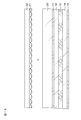
- FIG. 1 is a schematic perspective view when the display device used in the first embodiment is virtually separated.
- FIG. 2 is a schematic cross-sectional view of a part of the display device.
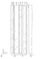
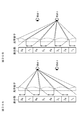
- FIG. 3 is a schematic plan view of a part of a display region in a display unit having a structure in which pixels having different planar shapes are alternately arranged for each row.
- FIG. 4 is a schematic plan view of a part of the optical element and the display region for explaining the positional relationship between the structure of the optical element and the pixels in the display region of the display unit.
- FIG. 5 is a schematic plan view of a part of the optical element and the display region for explaining the arrangement relationship between the structure of the optical element and the pixel in the embodiment of the reference example.
- FIG. 1 is a schematic perspective view when the display device used in the first embodiment is virtually separated.
- FIG. 2 is a schematic cross-sectional view of a part of the display device.
- FIG. 3 is a schematic plan view of a part of a display region in
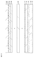
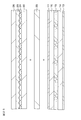
- FIG. 6 is a drawing-substituting photograph for explaining moire in the embodiment of the reference example.
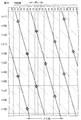
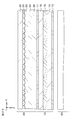
- FIG. 7 is a schematic plan view for explaining the relationship between the inclination of the structure of the optical element and the observed pixel.
- FIG. 9 shows the vertical center position of a certain color of a pixel group observed through a certain structure in the state shown in FIG. It is a typical top view for demonstrating the vertical center position of this certain color of the pixel group observed through a structure.
- FIG. 9 shows the vertical center position of a certain color of a pixel group observed through a certain structure in the state shown in FIG. It is a typical top view for demonstrating the vertical center position of this certain color of the pixel group observed through a structure.
- 11A and 11B are diagrams for explaining the difference between the case where the symbol NP is an odd number and the case where the number NP is an even number, and FIG. 11A shows an extracted central position shown in FIG.
- FIG. 11B is an extracted view of the observed central position shown in FIG. FIG.
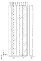
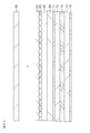
- FIG. 12 is a drawing-substituting photograph for explaining moire in the first embodiment.
- FIG. 13 is a schematic cross-sectional view of a part of the display device for explaining the refractive index of the constituent elements of the optical element.
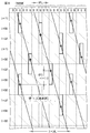
- FIG. 14 is a schematic graph for explaining the shape of the lens array constituting the structure when it is cut along a plane whose normal direction is the direction in which the lens array extends.
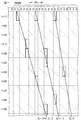
- FIG. 15 is a schematic graph for explaining the relationship between the E hardness of the resin layer and the degree of unevenness.
- FIG. 16 is a schematic graph for explaining the thickness of the resin layer and the degree of peeling.
- FIG. 17A to FIG. 17C are schematic views for explaining a method for manufacturing an optical element or the like used in the first embodiment.
- FIG. 18A and 18B are schematic views for explaining a manufacturing method of the optical element and the like used in the first embodiment, following FIG. 17C.
- FIG. 19 is a schematic diagram for explaining a manufacturing method of the optical element and the like used in the first embodiment, following FIG. 18B.
- FIG. 20 is a schematic cross-sectional view of a part of the display device according to the first modification of the first embodiment.
- 21A to 21C are schematic views for explaining a method for manufacturing an optical element or the like used in the first modification of the first embodiment.
- FIG. 22 is a schematic diagram for explaining a manufacturing method of the optical element and the like used in the first modification of the first embodiment, following FIG. 21C.
- FIG. 21C is a schematic diagram for explaining a manufacturing method of the optical element and the like used in the first modification of the first embodiment, following FIG. 21C.
- FIG. 23 is a schematic cross-sectional view of a part of the display device according to the second modification of the first embodiment.
- 24A to 24C are schematic views for explaining a method for manufacturing an optical element or the like used in the second modification of the first embodiment.
- FIG. 25 is a schematic diagram for explaining a manufacturing method of an optical element and the like used in the second modification of the first embodiment, following FIG. 24C.
- FIG. 26 is a schematic diagram for explaining another manufacturing method such as an optical element used in the second modification of the first embodiment.
- FIG. 27 is a schematic cross-sectional view of a part of the display device according to the third modification of the first embodiment.
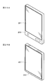
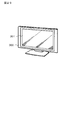
- FIG. 28A and FIG. 28B each show the appearance of a smartphone to which the display device of the embodiment is applied.
- FIG. 29 illustrates an appearance of a television device to which the display device of the embodiment is applied.
- 30A and 30B are conceptual diagrams of a naked-eye display device.
- display device of the present disclosure or the display device used in the electronic device of the present disclosure (hereinafter, these may be collectively referred to simply as “display device of the present disclosure”).
- the pixels in the display area constitute a group of three pixels arranged in the row direction
- the pitch in the horizontal direction of the structure of the optical element in units of the number of pixels is denoted by a symbol LM X
- the inclination of the structure in units of the number of pixels is denoted by SL
- a deviation in the vertical direction from the vertical center position of the certain color in units of the number of pixels is denoted by OFS
- the sign LM X is a non-integer
- the display device of the present disclosure including the various preferable configurations described above, In the display area, two types of pixels having different planar shapes are alternately arranged for each row. It can be configured.
- the display unit consists of a liquid crystal display panel. It can be configured.
- the optical element A substrate, and A lenticular lens part formed on a base material, wherein a plurality of lenses constituting the structure are arranged; Contains Between the lenticular lens part and the flat plate facing the lenticular lens part, the material constituting the lenticular lens part is filled with a resin layer having a different refractive index, It can be configured.
- optical element of the present disclosure and the optical element used in the display device of the present disclosure including the various preferred configurations described above (hereinafter, these may be collectively referred to simply as “optical element of the present disclosure”).
- the lens constituting the structure is aspherical, It can be configured.
- the lens constituting the structure is a convex lens shape
- the resin layer is made of a resin material having a refractive index lower than that of the material constituting the structure. Can be configured, and The refractive index of the resin layer is a value between 1.2 and 1.4. It can be configured.
- the lens constituting the structure is a concave lens shape
- the resin layer is made of a resin material having a refractive index higher than that of the material constituting the structure. Can be configured, and The refractive index of the resin layer is a value between 1.6 and 1.8. It can be configured.
- the film thickness of the resin layer is 40 micrometers or more. It can be configured.
- E hardness of the resin layer is 30 or less, It can be configured.
- the elastic modulus of the resin layer is 500 kPa or less, It can be configured.
- the resin layer is made of an ultraviolet curable resin material. It can be configured.
- the image for the right eye is displayed on the entire surface of the image.
- the image data corresponding to the pixel on which the image for the right eye is to be displayed is selected from the image data for the right eye, and the pixel is driven to display the image for the left eye on the entire display area.
- the image data corresponding to the pixel on which the left-eye image is to be displayed can be selected from the left-eye image data to drive the pixel.
- the display device may be configured such that an optical element is disposed between the display unit and the image observer.
- an optical element is disposed between the display unit and the image observer.
- a liquid crystal display panel, an electroluminescence display panel, or the like can be used as the display portion.
- the display unit may be a monochrome display or a color display.
- the configuration and arrangement of the optical elements may be set as appropriate according to the specifications of the display device.
- a parallax barrier is used as the optical element, a fixed parallax barrier or a dynamically switchable parallax barrier may be used.
- a fixed parallax barrier is a combination of a photolithographic method and an etching method, a screen printing method, an ink jet printing method, a metal mask printing method, etc., using a base material made of a known transparent material such as resin or glass. It can be formed by a known method such as a printing method, a plating method (electroplating method or electroless plating method), a lift-off method, or the like.
- the dynamically switchable parallax barrier can be configured by, for example, an electrically switchable light valve including a liquid crystal material layer. There are no particular limitations on the type of material constituting the light valve using the liquid crystal material layer and the operation mode of the liquid crystal material layer.
- a monochrome display liquid crystal display panel can be used as a dynamic parallax barrier. What is necessary is just to set suitably the magnitude
- a lens sheet when used as the optical element, a lens sheet in which a lens array is formed using a photosensitive resin material or the like on a sheet-like base material made of a known transparent material may be used.
- the display device includes a transmissive display panel and an illumination unit
- a widely known illumination unit can be used.
- the configuration of the illumination unit is not particularly limited.
- the illuminating unit can be formed of a known member such as a light source, a prism sheet, a diffusion sheet, a light guide plate, and the like.
- an active matrix type transmissive liquid crystal display panel is used as a display unit, and an optical element in which a lens array as a structure is formed is used.
- the liquid crystal display panel is made of, for example, a front panel having a transparent common electrode, a rear panel having a transparent pixel electrode, and a liquid crystal material disposed between the front panel and the rear panel.
- the operation mode of the liquid crystal display panel is not particularly limited. It may be configured to be driven in a so-called TN mode, or may be configured to be driven in a VA mode or an IPS mode.
- a color liquid crystal display panel a color filter covered with an overcoat layer made of acrylic resin or epoxy resin is provided on the inner surface of the substrate, and a transparent common electrode is formed on the overcoat layer. Yes.
- the values of the resolution (P, Q) of the display unit are VGA (640, 480), S-VGA (800, 600), XGA (1024, 768), APRC (1152, 900), S- XGA (1280, 1024), U-XGA (1600, 1200), HD-TV (1920, 1080), Q-XGA (2048, 1536), QFHD (3840, 2160), (1920, 1035), ( 720, 480) and (1280, 960) can be exemplified as some of the image display resolutions, but are not limited to these values.
- the driving unit that drives the display unit can be configured by various circuits such as an image signal processing unit, a timing control unit, a data driver, and a gate driver. These can be configured using known circuit elements or the like.
- FIG. 1 is a schematic perspective view when a display device used in the embodiment is virtually separated.
- a display unit 10 having a display area 11 for displaying a two-dimensional image, and An optical element 30 in which a plurality of structures 31 for separating an image displayed in the display area 11 into images observed at predetermined observation positions arranged at intervals in the horizontal direction are arranged; It has.
- the display unit 10 is driven by the driving unit 100.
- pixels 12 are arranged in a matrix in the horizontal direction and in the vertical direction, and pixels having different planar shapes are arranged in a fixed cycle for each row.
- the structure 31 of the optical element 30 is arranged so as to be inclined with respect to the vertical direction with an inclination satisfying (J + 0.5) / 3 (where J is an integer of 3 or more) with the number of pixels 12 as a unit. .
- J is an integer of 3 or more
- the driving unit 100 includes: Selecting image data corresponding to the pixel 12 on which the right-eye image is to be displayed from the right-eye image data for displaying the right-eye image on the entire surface of the display area 11, and driving the pixel 12; Image data corresponding to the pixel 12 on which the image for the left eye is to be displayed is selected from the image data for the left eye that displays the image for the left eye on the entire display area 11, and the pixel 12 is driven. It is also possible to adopt a configuration in which the position of the observer's head is detected and actively controlled.
- the display unit 10 is composed of a liquid crystal display panel, more specifically, an IPS color liquid crystal display panel. On the back surface of the display unit 10, an illumination unit 20 that emits light is disposed.
- FIG. 2 is a schematic cross-sectional view of a part of the display device.
- the display unit 10 includes a front panel 16 on the optical element 30 side, a rear panel 14 on the illumination unit 20 side, a liquid crystal material layer 15 disposed between the front panel 16 and the rear panel 14, and the like.
- the wiring layer and the light shielding layer are not shown.
- a polarizing plate 13 is disposed on the surface of the rear panel 14 on the illumination unit 20 side, and a polarizing plate 17 is disposed on the surface of the front panel 16.
- the polarizing plates 13 and 17 are arranged so as to have a crossed Nicols or parallel Nicols relationship according to the specifications of the display unit 10.
- the illumination unit 20 is composed of members such as a light source, a prism sheet, a diffusion sheet, and a light guide plate (these are not shown). Diffused light via a diffusion sheet or the like is irradiated from the light emitting surface 21 shown in FIG. 1 toward the back surface of the display unit 10.
- an optical element 30 On the front side of the display unit 10, there is disposed an optical element 30 in which a plurality of structures 31 made of lenticular lenses are arranged.
- the distance in the Z direction between the optical element 30 and the display unit 10, the pitch in the X direction of the pixels 12 in the X direction, the angle formed by the direction in which the opening 31 extends and the Y direction, and the pitch in the X direction of the opening 31 are displayed. It is set so as to satisfy a condition that a preferable stereoscopic image can be observed at the observation position defined in the specification of the apparatus 1.
- observation position A U / 4 corresponds to the reference position for the right eye
- observation position A 3U / 4 corresponds to the reference position for the left eye.
- the value of the code U may be set according to the specification of the display device 1 and may be a value such as 24, for example.
- the optical element 30 includes a base material 32 and a lenticular lens portion formed on the base material 32 and formed by arranging a plurality of lenses constituting the structure 31.
- reference numeral 31 may be used to indicate the lenticular lens portion.
- the space between the lenticular lens unit 31 and the flat plate (here, the liquid crystal display panel constituting the display unit 10) facing the lenticular lens unit 31 is filled with a resin layer 33 having a refractive index different from that of the material constituting the lenticular lens unit 31.
- the lens constituting the structure 31 has an aspherical convex lens shape, and the resin layer 33 is made of a resin material having a refractive index lower than that of the material constituting the structure 31.
- FIG. 3 is a schematic plan view of a part of the display area in the display unit having a structure in which pixels having different planar shapes are alternately arranged for each row.
- P pixels in the horizontal direction (X direction in the drawing), Q pixels in the vertical direction (Y direction in the drawing), and a total of P ⁇ Q pixels 12 are arranged in a matrix.
- a black matrix BM is provided between the pixels 12 and 12.
- the red display pixel, the green display pixel, and the blue display pixel are represented by using symbols R, G, and B, respectively.
- pixels 12 having different planar shapes are arranged at regular intervals for each row.
- two types of pixels having different planar shapes are alternately arranged in the display area 11 for each row. That is, a pixel 12 having a shape inclined in the (+ X, + Y) direction (hereinafter referred to as [A type]) and a pixel 12 having a shape inclined in the ( ⁇ X, + Y) direction (hereinafter referred to as [B type]). 12 are alternately arranged in each row.
- the pixels 12 are arranged in the order of a red display pixel in the first column, a green display pixel in the second column, and a blue display pixel in the third column, and the same order is applied to the fourth and subsequent columns. Arranged to repeat.
- the pixels in the display area 11 constitute a pixel group composed of three pixels arranged in the row direction. That is, one pixel group is configured by three red display pixels, green display pixels, and blue display pixels arranged in the row direction.
- the display unit 10 has a size of about 13 inches diagonal, for example.
- FIG. 4 is a schematic plan view of a part of the optical element and the display region for explaining the positional relationship between the structure of the optical element and the pixels in the display region of the display unit.
- the pixels are described as having virtually the same rectangular and plane-filled shape.
- the pitch in the X direction of the pixel is denoted by a symbol PL X
- the structure 31 of the optical element 30 is disposed so as to be inclined with respect to the vertical direction.
- the inclination is represented by reference sign SL.
- FIG. 5 is a schematic plan view of a part of the optical element and the display region for explaining the arrangement relationship between the structure of the optical element and the pixel in the embodiment of the reference example.
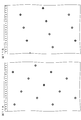
- FIG. 6 is a drawing-substituting photograph for explaining moire in the embodiment of the reference example.
- a symbol LM X in FIG. 5 represents the arrangement pitch of the structures 31 in the X direction.
- the arrangement pitch LM X (24/5) ⁇ PL X is set.
- the A-type pixel 12 is mainly observed at a certain position and the B-type pixel 12 is mainly observed at other positions due to the arrangement relationship with the pixels having different shapes for each row.
- the phenomenon of being observed in This causes moiré.
- the right side of FIG. 6 shows an image by simulation, and the left side of FIG. 6 shows a photograph of the actual machine. The streak-like moire significantly reduces the quality of the displayed image.
- the inventor has determined that the structure 31 of the optical element 30 has an inclination satisfying (J + 0.5) / 3 with respect to the vertical direction in units of the number of pixels 12 (where J is an integer of 3 or more). It has been found that the degree of streaky moire can be reduced by arranging them so as to be inclined.
- FIG. 7 is a schematic plan view for explaining the relationship between the tilt of the optical element structure and the observed pixels.
- the difference in shape is represented by [A type] and [B type], and in the drawing, it is represented as a virtually identical rectangular and plane-filled shape.
- the pixels in the display area constitute a group of three pixels arranged in the row direction
- the pitch in the horizontal direction of the structure of the optical element in units of the number of pixels is denoted by a symbol LM X
- the inclination of the structure in units of the number of pixels is denoted by SL
- a deviation in the vertical direction from the vertical center position of the certain color in units of the number of pixels is denoted by OFS
- a pixel of a specific color (in this case, green) observed from a certain viewpoint is surrounded by a thick line, and a circle is added to the center of the pixel in the horizontal direction.
- FIG. 9 shows the vertical center position of a certain color of a pixel group observed through a certain structure in the state shown in FIG. It is a typical top view for demonstrating the vertical center position of this certain color of the pixel group observed through a structure.
- the centers of the certain color of the pixel group observed through the structure are distributed at a predetermined period on a line extending along the structure.
- the adjacent structures are distributed with a shift of about a half cycle.
- the vertical center position of a certain color and the vertical center position of the certain color of a pixel group observed through a structure lined up with one structure with respect to a certain structure It is a typical top view for doing.
- the center of the certain color of the pixel group observed through the structure is distributed with a predetermined period on a line extending along the structure. However, there is little period shift between adjacent structures.
- FIG. 11A and 11B are diagrams for explaining the difference between the case where the symbol NP is an odd number and the case where the number NP is an even number, and FIG. 11A shows an extracted central position shown in FIG. FIG. 11B is an extracted view of the observed central position shown in FIG.
- FIG. 11A in the case where the code NP is an odd number reduces the degree of alignment of the pixels on the line as compared to FIG. 11B in which the code NP is an even number. Accordingly, the degree of the stripe pattern based on the distribution of the center of the pixel is also reduced.
- FIG. 12 is a drawing-substituting photograph for explaining moire in the first embodiment.
- the right side of FIG. 12 shows an image by simulation, and the left side of FIG. 12 shows a photograph of the actual machine. It can be seen that the vertical stripes are reduced compared to FIG.
- FIG. 13 is a schematic cross-sectional view of a part of the display device for explaining the refractive index of the constituent elements of the optical element.
- FIG. 13 shows a configuration of a reference example in which a front plate is disposed in front of a lenticular lens.
- the front plate is opposed to the lenticular lens portion via the spacer.
- the base material 32 is comprised from transparent materials, such as soda glass and an acryl, and a refractive index is about 1.5.
- the lenticular lens unit 31 is made of an ultraviolet curable resin material.
- the refractive index n L of the lenticular lens portion 31 is approximately 1.5.
- the base material 32 and the display part 10 are adhere
- the front plate is made of a transparent material such as soda glass or acrylic and has a refractive index n P ⁇ 1.5.
- the air gap is an air layer, and the refractive index n Air of the air layer is approximately 1.0.
- This configuration has problems such that reflection occurs due to the interface between the front plate and the air layer, and the contrast is lowered and overlapping images are observed.
- FIG. 13 shows the configuration of the first embodiment.
- the space between the lenticular lens unit 31 and the flat plate (here, the liquid crystal display panel constituting the display unit 10) facing the lenticular lens unit 31 is filled with a resin layer 33 having a refractive index different from that of the material constituting the lenticular lens unit 31.
- the refractive index n M of the resin layer 33 is set so as to satisfy the relationship n Air ⁇ n M ⁇ n L.
- the curvature of the lens since the refractive index difference at the interface of the lenticular lens portion is reduced, the curvature of the lens must be increased. However, simply increasing the curvature increases the aberration.
- FIG. 14 is a schematic graph for explaining the shape of the lens array constituting the structure when it is cut along a plane whose normal direction is the direction in which the lens array extends.
- the solid line shows the aspherical shape adopted this time, and the broken line shows the spherical reference shape.
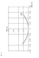
- the hardness of the resin layer 33 was changed, and a 10-point evaluation of 5 points out of brightness unevenness was performed.
- the film thickness of the resin layer 33 was approximately 90 micrometers. The results are shown in FIG.
- the sensory evaluation has an evaluation of 3.0 or more, luminance unevenness is allowed. From the results, it was found that the brightness unevenness was good when the E hardness was 30 or less, more preferably 10 or less.
- the E hardness was measured using a durometer type E. From the same viewpoint, the elastic modulus of the resin layer 33 is preferably 500 kPa or less.
- the resin layer 33 has a film thickness of a certain degree or more from the viewpoint of adhesive strength.
- the film thickness was changed to evaluate peeling. The results are shown in FIG.
- the film thickness of the resin layer 33 is preferably 40 micrometers or more.
- FIG. 17A to FIG. 17C are schematic views for explaining a method for manufacturing an optical element or the like used in the first embodiment.
- 18A and 18B are schematic views for explaining a manufacturing method of the optical element and the like used in the first embodiment, following FIG. 17C.
- a base material 32 made of a transparent material is prepared (FIG. 17A), and an ultraviolet curable resin material is applied to the surface using a well-known application method to form a material layer 31 '(FIG. 17B). Thereafter, a lens molding mask 39 is placed on the material layer 31 ′, and ultraviolet rays are irradiated from the base material 32 side (FIG. 17C).
- the lenticular lens part 31 is formed on the base material 32 by removing the mask 39 (FIG. 18A).
- an ultraviolet curable resin material that is the base of the resin layer 33 is applied on the display unit 10 by using a known application method to form a material layer 33 ′ (FIG. 18B).
- the material layer 33 ′ and the lenticular lens portion 31 are overlaid so as to face each other (FIG. 19). Thereafter, the resin layer 33 is formed by curing the material layer 33 ′ by irradiating ultraviolet rays.
- FIG. 20 is a schematic cross-sectional view of a part of the display device according to the first modification of the first embodiment.
- a laminate including the base material 32, the lenticular lens portion 31, the material layer 33, and the film 34 is first formed, and the laminate and the display portion 10 are bonded to each other with the adhesive layer 35.
- the lenticular lens portion 31 is formed on the substrate 32 (FIG. 21A).
- an ultraviolet curable resin material that is a base of the resin layer 33 is applied on the lenticular lens portion 31 by using a known application method to form a material layer 33 ′ (FIG. 21B).
- a film 34 made of PET, for example is stacked and irradiated with ultraviolet rays to form a laminate (FIG. 21C).
- FIG. 23 is a schematic cross-sectional view of a part of the display device according to the second modification of the first embodiment.
- the second modification is a configuration in which the base material 32 and the display unit 10 are bonded by the adhesive layer 35.
- the lenticular lens portion 31 is formed on the base material 32 (FIG. 24A).
- an ultraviolet curable resin material that is the base of the resin layer 33 is applied on the lenticular lens portion 31 by using a known application method to form a material layer 33 ′ (FIG. 24B).
- a front plate 36 made of a glass material is stacked and irradiated with ultraviolet rays to form a laminate (FIG. 24C).
- a material layer 33 ′ is formed on the lenticular lens unit 31, and then a front plate 36 made of, for example, a glass material is overlaid. It is good also as a structure which irradiates an ultraviolet-ray (FIG. 26).
- FIG. 27 is a schematic cross-sectional view of a part of the display device according to the third modification of the first embodiment.
- the lens constituting the structure 31 has a concave lens shape.
- the resin layer 33 is made of a resin material having a higher refractive index than the material constituting the structure 31.
- the refractive index n L of the structure 31 is preferably 1.3 and the refractive index n M of the resin layer 33 is preferably 1.6 to 1.8.
- FIG. 28A and FIG. 28B each show the appearance of a smartphone to which the display device of the above embodiment is applied.
- the smartphones 200 and 200 ′ have, for example, video display screen portions 201 and 201 ′.
- the video display screen portions 200 and 201 ′ are configured by the display device of the above embodiment.
- FIG. 29 illustrates an appearance of a television device to which the display device of the above embodiment is applied.
- the television apparatus 300 includes a video display screen unit 301, for example.
- This video display screen unit 301 is configured by the display device of the embodiment.
- a stereoscopic image with little crosstalk can be displayed by applying the display device of the above embodiment, which contributes to improving the quality of the television device 300. can do.
- the present disclosure is not limited to the above-described embodiment, and various modifications based on the technical idea of the present disclosure are possible.
- the numerical values, structures, substrates, raw materials, processes, and the like given in the above-described embodiments are merely examples, and different numerical values, structures, substrates, raw materials, processes, and the like may be used as necessary.
- a display unit having a display area for displaying a two-dimensional image, and An optical element in which a plurality of structures for separating an image displayed in a display area into images observed at predetermined observation positions arranged at intervals in the horizontal direction are arranged;
- pixels are arranged in a matrix in the horizontal direction and the vertical direction, and pixels having different planar shapes are arranged in a fixed cycle for each row,
- the structure of the optical element is disposed so as to be inclined with respect to the vertical direction with an inclination satisfying (J + 0.5) / 3 (where J is an integer of 3 or more) with the number of pixels as a unit.
- the pixels in the display area constitute a group of three pixels arranged in the row direction,
- the pitch in the horizontal direction of the structure of the optical element in units of the number of pixels is denoted by a symbol LM X
- the inclination of the structure in units of the number of pixels is denoted by SL
- a deviation in the vertical direction from the vertical center position of the certain color in units of the number of pixels is denoted by OFS
- the display unit consists of a liquid crystal display panel.
- the optical element A substrate, and A lenticular lens part formed on a base material, wherein a plurality of lenses constituting the structure are arranged; Contains Between the lenticular lens part and the flat plate facing the lenticular lens part, the material constituting the lenticular lens part is filled with a resin layer having a different refractive index, The display device according to any one of [A1] to [A4].
- the lens constituting the structure is aspherical, The display device according to [A5] above.
- the lens constituting the structure is a convex lens shape,
- the resin layer is made of a resin material having a refractive index lower than that of the material constituting the structure.
- the refractive index of the resin layer is a value between 1.2 and 1.4.
- the lens constituting the structure is a concave lens shape,
- the resin layer is made of a resin material having a refractive index higher than that of the material constituting the structure.
- the refractive index of the resin layer is a value between 1.6 and 1.8.
- the film thickness of the resin layer is 40 micrometers or more.
- E hardness of the resin layer is 30 or less, The display device according to any one of [A5] to [A11].
- the elastic modulus of the resin layer is 500 kPa or less, The display device according to any one of [A5] to [A12].
- the resin layer is made of an ultraviolet curable resin material.
- [B1] A substrate, and A lenticular lens part formed on a base material, wherein a plurality of lenses constituting the structure are arranged; Contains Between the lenticular lens part and the flat plate facing the lenticular lens part, the material constituting the lenticular lens part is filled with a resin layer having a different refractive index, Optical element.
- the lens constituting the structure is aspherical, The optical element according to the above [B1].
- [B3] The lens constituting the structure is a convex lens shape, The resin layer is made of a resin material having a refractive index lower than that of the material constituting the structure.
- the refractive index of the resin layer is a value between 1.2 and 1.4.
- the lens constituting the structure is a concave lens shape,
- the resin layer is made of a resin material having a refractive index higher than that of the material constituting the structure.
- the refractive index of the resin layer is a value between 1.6 and 1.8.
- the film thickness of the resin layer is 40 micrometers or more. The optical element according to any one of [B1] to [B6].
- E hardness of the resin layer is 30 or less, The optical element according to any one of [B1] to [B7].
- the elastic modulus of the resin layer is 500 kPa or less, The optical element according to any one of [B1] to [B8].
- the resin layer is made of an ultraviolet curable resin material.
- the flat plate consists of a liquid crystal display panel, The optical element according to any one of [B1] to [B10].
- the display device A display unit having a display area for displaying a two-dimensional image, and An optical element in which a plurality of structures for separating an image displayed in a display area into images observed at predetermined observation positions arranged at intervals in the horizontal direction are arranged; With In the display area, pixels are arranged in a matrix in the horizontal direction and the vertical direction, and pixels having different planar shapes are arranged in a fixed cycle for each row, The structure of the optical element is disposed so as to be inclined with respect to the vertical direction with an inclination satisfying (J + 0.5) / 3 (where J is an integer of 3 or more) with the number of pixels as a unit. Electronics.
- the pixels in the display area constitute a group of three pixels arranged in the row direction,
- the pitch in the horizontal direction of the structure of the optical element in units of the number of pixels is denoted by a symbol LM X
- the inclination of the structure in units of the number of pixels is denoted by SL
- a deviation in the vertical direction from the vertical center position of the certain color in units of the number of pixels is denoted by OFS
- the display unit consists of a liquid crystal display panel.
- the optical element A substrate, and A lenticular lens part formed on a base material, wherein a plurality of lenses constituting the structure are arranged; Contains Between the lenticular lens part and the flat plate facing the lenticular lens part, the material constituting the lenticular lens part is filled with a resin layer having a different refractive index, The electronic device according to any one of [C1] to [C4].
- the lens constituting the structure is aspherical, The electronic device according to [C5] above.
- the lens constituting the structure is a convex lens shape,
- the resin layer is made of a resin material having a refractive index lower than that of the material constituting the structure.
- the refractive index of the resin layer is a value between 1.2 and 1.4.
- the lens constituting the structure is a concave lens shape,
- the resin layer is made of a resin material having a refractive index higher than that of the material constituting the structure.
- the refractive index of the resin layer is a value between 1.6 and 1.8.
- the film thickness of the resin layer is 40 micrometers or more.
- E hardness of the resin layer is 30 or less, The electronic device according to any one of [C5] to [C11].
- the elastic modulus of the resin layer is 500 kPa or less, The electronic device according to any one of [C5] to [C12].
- the resin layer is made of an ultraviolet curable resin material.
- DESCRIPTION OF SYMBOLS 1 ... Display apparatus, 10 ... Display part, 11 ... Display area, 12 ... Pixel, 13 ... Polarizing plate, 14 ... Substrate, 15 ... Liquid crystal material layer, 16 * ..Substrate, 17 ... polarizing plate, 20 ... illumination part, 21 ... light emitting surface, 30 ... optical element, 31 ... structure (lenticular lens part), 31 '... material Layer, 32 ... base material, 33 ... resin layer, 33 '... material layer, 34 ... film, 35 ... adhesive layer, 32 ... base material, 40 ... optical element , 41 ... structure, 42 ... base material, 43 ... low refractive resin layer, 44 ... front plate, 45 ... substrate, 100 ...
Landscapes
- Physics & Mathematics (AREA)
- General Physics & Mathematics (AREA)
- Optics & Photonics (AREA)
- Nonlinear Science (AREA)
- Engineering & Computer Science (AREA)
- Multimedia (AREA)
- Signal Processing (AREA)
- Geometry (AREA)
- Chemical & Material Sciences (AREA)
- Crystallography & Structural Chemistry (AREA)
- Mathematical Physics (AREA)
- Liquid Crystal (AREA)
- Testing, Inspecting, Measuring Of Stereoscopic Televisions And Televisions (AREA)
- Stereoscopic And Panoramic Photography (AREA)
Priority Applications (1)
| Application Number | Priority Date | Filing Date | Title |
|---|---|---|---|
| US16/088,180 US11169392B2 (en) | 2016-03-30 | 2017-03-07 | Display apparatus, optical element, and electronic apparatus |
Applications Claiming Priority (2)
| Application Number | Priority Date | Filing Date | Title |
|---|---|---|---|
| JP2016-068975 | 2016-03-30 | ||
| JP2016068975A JP2017181787A (ja) | 2016-03-30 | 2016-03-30 | 表示装置、光学素子、及び、電子機器 |
Publications (1)
| Publication Number | Publication Date |
|---|---|
| WO2017169566A1 true WO2017169566A1 (ja) | 2017-10-05 |
Family
ID=59963022
Family Applications (1)
| Application Number | Title | Priority Date | Filing Date |
|---|---|---|---|
| PCT/JP2017/008985 Ceased WO2017169566A1 (ja) | 2016-03-30 | 2017-03-07 | 表示装置、光学素子、及び、電子機器 |
Country Status (3)
| Country | Link |
|---|---|
| US (1) | US11169392B2 (enExample) |
| JP (1) | JP2017181787A (enExample) |
| WO (1) | WO2017169566A1 (enExample) |
Cited By (2)
| Publication number | Priority date | Publication date | Assignee | Title |
|---|---|---|---|---|
| CN111193921A (zh) * | 2020-01-10 | 2020-05-22 | 吉林大学 | 一种基于组合离散光栅的led屏一维集成成像显示方法 |
| CN111198448A (zh) * | 2020-01-10 | 2020-05-26 | 吉林大学 | 一种基于异形柱透镜光栅的一维集成成像显示方法 |
Families Citing this family (7)
| Publication number | Priority date | Publication date | Assignee | Title |
|---|---|---|---|---|
| KR102625625B1 (ko) | 2017-08-23 | 2024-01-15 | 인터디지털 매디슨 페턴트 홀딩스 에스에이에스 | 투사형 3d 라이트 필드 생성을 위한 라이트 필드 이미지 방법 및 장치 |
| JP7246311B2 (ja) | 2017-09-21 | 2023-03-27 | テルモ株式会社 | 薬剤コート層およびその形成方法 |
| US11624934B2 (en) | 2017-11-02 | 2023-04-11 | Interdigital Madison Patent Holdings, Sas | Method and system for aperture expansion in light field displays |
| KR102555999B1 (ko) * | 2018-07-23 | 2023-07-14 | 삼성디스플레이 주식회사 | 표시 장치 |
| CN112868227B (zh) * | 2018-08-29 | 2024-04-09 | Pcms控股公司 | 用于基于镶嵌周期性层的光场显示的光学方法及系统 |
| CN115079435B (zh) * | 2020-08-03 | 2024-09-03 | 京东方科技集团股份有限公司 | 显示组件、显示装置和驱动方法 |
| KR20220145039A (ko) * | 2021-04-21 | 2022-10-28 | 삼성전자주식회사 | 렌티큘러 렌즈 및 이를 포함하는 3d hud용 디스플레이 장치 |
Citations (5)
| Publication number | Priority date | Publication date | Assignee | Title |
|---|---|---|---|---|
| WO2011033618A1 (ja) * | 2009-09-16 | 2011-03-24 | 株式会社 東芝 | 立体画像表示装置 |
| JP2011524541A (ja) * | 2008-06-02 | 2011-09-01 | コーニンクレッカ フィリップス エレクトロニクス エヌ ヴィ | 光学装置及びその光学装置を組み込んだ自動立体視ディスプレイ装置 |
| US20120092763A1 (en) * | 2010-10-19 | 2012-04-19 | Shenzhen Super Perfect Optics Limited | Autostereoscopic display apparatus and method |
| JP2013217951A (ja) * | 2012-04-04 | 2013-10-24 | Jvc Kenwood Corp | 裸眼立体ディスプレイ装置 |
| WO2014147100A1 (en) * | 2013-03-22 | 2014-09-25 | Koninklijke Philips N.V. | Autostereoscopic display device |
Family Cites Families (6)
| Publication number | Priority date | Publication date | Assignee | Title |
|---|---|---|---|---|
| JPH05122733A (ja) | 1991-10-28 | 1993-05-18 | Nippon Hoso Kyokai <Nhk> | 3次元画像表示装置 |
| JP2001141909A (ja) * | 1999-11-17 | 2001-05-25 | Seiko Epson Corp | マイクロレンズ基板、液晶パネル用対向基板、液晶パネルおよび投射型表示装置 |
| JP2014202916A (ja) * | 2013-04-04 | 2014-10-27 | 株式会社カネカ | 画像表示装置、およびそれを搭載した電気、電子機器 |
| KR102308388B1 (ko) * | 2013-12-20 | 2021-10-05 | 코닌클리케 필립스 엔.브이. | 무안경식 디스플레이 디바이스 |
| JP2015219422A (ja) * | 2014-05-19 | 2015-12-07 | Nltテクノロジー株式会社 | 光学部材及び表示装置 |
| JP2016011976A (ja) * | 2014-06-27 | 2016-01-21 | 日本化薬株式会社 | 光学部材の製造方法及びそれに用いる紫外線硬化型樹脂組成物 |
-
2016
- 2016-03-30 JP JP2016068975A patent/JP2017181787A/ja active Pending
-
2017
- 2017-03-07 WO PCT/JP2017/008985 patent/WO2017169566A1/ja not_active Ceased
- 2017-03-07 US US16/088,180 patent/US11169392B2/en active Active
Patent Citations (5)
| Publication number | Priority date | Publication date | Assignee | Title |
|---|---|---|---|---|
| JP2011524541A (ja) * | 2008-06-02 | 2011-09-01 | コーニンクレッカ フィリップス エレクトロニクス エヌ ヴィ | 光学装置及びその光学装置を組み込んだ自動立体視ディスプレイ装置 |
| WO2011033618A1 (ja) * | 2009-09-16 | 2011-03-24 | 株式会社 東芝 | 立体画像表示装置 |
| US20120092763A1 (en) * | 2010-10-19 | 2012-04-19 | Shenzhen Super Perfect Optics Limited | Autostereoscopic display apparatus and method |
| JP2013217951A (ja) * | 2012-04-04 | 2013-10-24 | Jvc Kenwood Corp | 裸眼立体ディスプレイ装置 |
| WO2014147100A1 (en) * | 2013-03-22 | 2014-09-25 | Koninklijke Philips N.V. | Autostereoscopic display device |
Cited By (3)
| Publication number | Priority date | Publication date | Assignee | Title |
|---|---|---|---|---|
| CN111193921A (zh) * | 2020-01-10 | 2020-05-22 | 吉林大学 | 一种基于组合离散光栅的led屏一维集成成像显示方法 |
| CN111198448A (zh) * | 2020-01-10 | 2020-05-26 | 吉林大学 | 一种基于异形柱透镜光栅的一维集成成像显示方法 |
| CN111198448B (zh) * | 2020-01-10 | 2021-07-30 | 吉林大学 | 一种基于异形柱透镜光栅的一维集成成像显示方法 |
Also Published As
| Publication number | Publication date |
|---|---|
| JP2017181787A (ja) | 2017-10-05 |
| US11169392B2 (en) | 2021-11-09 |
| US20200301162A1 (en) | 2020-09-24 |
Similar Documents
| Publication | Publication Date | Title |
|---|---|---|
| WO2017169566A1 (ja) | 表示装置、光学素子、及び、電子機器 | |
| CN102819147B (zh) | 显示装置 | |
| CN102692720B (zh) | 显示装置 | |
| JP5607558B2 (ja) | 画像表示装置及び可変レンズアレイ | |
| US8558961B2 (en) | Display device and lenticular sheet of the display device | |
| TWI601980B (zh) | 自動立體顯示裝置 | |
| TWI471665B (zh) | 可切換二維與三維顯示模式之顯示裝置 | |
| US20100245406A1 (en) | Autostereoscopic display device | |
| JP5607430B2 (ja) | 立体映像表示装置及び電子機器 | |
| US20130278490A1 (en) | Display apparatus | |
| WO2017020473A1 (zh) | 三维显示装置及其显示方法 | |
| CN105629491A (zh) | 一种显示装置、裸眼3d显示系统和虚拟现实眼镜 | |
| US10630955B2 (en) | Display device, method of driving display device, and electronic device | |
| JP6411257B2 (ja) | 表示装置及びその制御方法 | |
| KR20140064556A (ko) | 경계부 오류광을 제거한 렌티큘라 렌즈 필름을 구비한 평판형 입체 표시장치 | |
| JP2009157301A (ja) | 電気光学装置 | |
| JP2021060617A (ja) | 表示装置、及び、電子機器 | |
| WO2023216541A1 (zh) | 显示装置 | |
| JP5381423B2 (ja) | 電気光学装置および電子機器 | |
| JP2008180800A (ja) | 表示素子および表示装置 | |
| JP2005227743A (ja) | ライトバルブ、ライトバルブ用基板、それに用いられるマイクロレンズ部材、電気光学装置、及び電子機器 | |
| CN119213479B (zh) | 显示面板、显示组件和操作显示面板的方法 | |
| CN115509025A (zh) | 立体显示器 | |
| JP2012003099A (ja) | 立体画像表示装置 | |
| JP2009116187A (ja) | 表示素子 |
Legal Events
| Date | Code | Title | Description |
|---|---|---|---|
| NENP | Non-entry into the national phase |
Ref country code: DE |
|
| 121 | Ep: the epo has been informed by wipo that ep was designated in this application |
Ref document number: 17774111 Country of ref document: EP Kind code of ref document: A1 |
|
| 122 | Ep: pct application non-entry in european phase |
Ref document number: 17774111 Country of ref document: EP Kind code of ref document: A1 |