WO2017164406A1 - 電磁波吸収熱伝導シート、電磁波吸収熱伝導シートの製造方法及び半導体装置 - Google Patents
電磁波吸収熱伝導シート、電磁波吸収熱伝導シートの製造方法及び半導体装置 Download PDFInfo
- Publication number
- WO2017164406A1 WO2017164406A1 PCT/JP2017/012155 JP2017012155W WO2017164406A1 WO 2017164406 A1 WO2017164406 A1 WO 2017164406A1 JP 2017012155 W JP2017012155 W JP 2017012155W WO 2017164406 A1 WO2017164406 A1 WO 2017164406A1
- Authority
- WO
- WIPO (PCT)
- Prior art keywords
- electromagnetic wave
- heat conductive
- sheet
- wave absorbing
- absorbing heat
- Prior art date
- Legal status (The legal status is an assumption and is not a legal conclusion. Google has not performed a legal analysis and makes no representation as to the accuracy of the status listed.)
- Ceased
Links
Images


Classifications
-
- H—ELECTRICITY
- H10—SEMICONDUCTOR DEVICES; ELECTRIC SOLID-STATE DEVICES NOT OTHERWISE PROVIDED FOR
- H10W—GENERIC PACKAGES, INTERCONNECTIONS, CONNECTORS OR OTHER CONSTRUCTIONAL DETAILS OF DEVICES COVERED BY CLASS H10
- H10W40/00—Arrangements for thermal protection or thermal control
- H10W40/10—Arrangements for heating
-
- H—ELECTRICITY
- H05—ELECTRIC TECHNIQUES NOT OTHERWISE PROVIDED FOR
- H05K—PRINTED CIRCUITS; CASINGS OR CONSTRUCTIONAL DETAILS OF ELECTRIC APPARATUS; MANUFACTURE OF ASSEMBLAGES OF ELECTRICAL COMPONENTS
- H05K7/00—Constructional details common to different types of electric apparatus
- H05K7/20—Modifications to facilitate cooling, ventilating, or heating
- H05K7/2039—Modifications to facilitate cooling, ventilating, or heating characterised by the heat transfer by conduction from the heat generating element to a dissipating body
- H05K7/20436—Inner thermal coupling elements in heat dissipating housings, e.g. protrusions or depressions integrally formed in the housing
- H05K7/20445—Inner thermal coupling elements in heat dissipating housings, e.g. protrusions or depressions integrally formed in the housing the coupling element being an additional piece, e.g. thermal standoff
- H05K7/20472—Sheet interfaces
- H05K7/20481—Sheet interfaces characterised by the material composition exhibiting specific thermal properties
-
- H—ELECTRICITY
- H05—ELECTRIC TECHNIQUES NOT OTHERWISE PROVIDED FOR
- H05K—PRINTED CIRCUITS; CASINGS OR CONSTRUCTIONAL DETAILS OF ELECTRIC APPARATUS; MANUFACTURE OF ASSEMBLAGES OF ELECTRICAL COMPONENTS
- H05K7/00—Constructional details common to different types of electric apparatus
- H05K7/20—Modifications to facilitate cooling, ventilating, or heating
- H05K7/20009—Modifications to facilitate cooling, ventilating, or heating using a gaseous coolant in electronic enclosures
- H05K7/20209—Thermal management, e.g. fan control
-
- H—ELECTRICITY
- H05—ELECTRIC TECHNIQUES NOT OTHERWISE PROVIDED FOR
- H05K—PRINTED CIRCUITS; CASINGS OR CONSTRUCTIONAL DETAILS OF ELECTRIC APPARATUS; MANUFACTURE OF ASSEMBLAGES OF ELECTRICAL COMPONENTS
- H05K9/00—Screening of apparatus or components against electric or magnetic fields
-
- H—ELECTRICITY
- H05—ELECTRIC TECHNIQUES NOT OTHERWISE PROVIDED FOR
- H05K—PRINTED CIRCUITS; CASINGS OR CONSTRUCTIONAL DETAILS OF ELECTRIC APPARATUS; MANUFACTURE OF ASSEMBLAGES OF ELECTRICAL COMPONENTS
- H05K9/00—Screening of apparatus or components against electric or magnetic fields
- H05K9/0073—Shielding materials
- H05K9/0081—Electromagnetic shielding materials, e.g. EMI, RFI shielding
- H05K9/0083—Electromagnetic shielding materials, e.g. EMI, RFI shielding comprising electro-conductive non-fibrous particles embedded in an electrically insulating supporting structure, e.g. powder, flakes, whiskers
-
- H—ELECTRICITY
- H05—ELECTRIC TECHNIQUES NOT OTHERWISE PROVIDED FOR
- H05K—PRINTED CIRCUITS; CASINGS OR CONSTRUCTIONAL DETAILS OF ELECTRIC APPARATUS; MANUFACTURE OF ASSEMBLAGES OF ELECTRICAL COMPONENTS
- H05K9/00—Screening of apparatus or components against electric or magnetic fields
- H05K9/0073—Shielding materials
- H05K9/0081—Electromagnetic shielding materials, e.g. EMI, RFI shielding
- H05K9/009—Electromagnetic shielding materials, e.g. EMI, RFI shielding comprising electro-conductive fibres, e.g. metal fibres, carbon fibres, metallised textile fibres, electro-conductive mesh, woven, non-woven mat, fleece, cross-linked
-
- H—ELECTRICITY
- H10—SEMICONDUCTOR DEVICES; ELECTRIC SOLID-STATE DEVICES NOT OTHERWISE PROVIDED FOR
- H10W—GENERIC PACKAGES, INTERCONNECTIONS, CONNECTORS OR OTHER CONSTRUCTIONAL DETAILS OF DEVICES COVERED BY CLASS H10
- H10W40/00—Arrangements for thermal protection or thermal control
- H10W40/20—Arrangements for cooling
- H10W40/22—Arrangements for cooling characterised by their shape, e.g. having conical or cylindrical projections
- H10W40/226—Arrangements for cooling characterised by their shape, e.g. having conical or cylindrical projections characterised by projecting parts, e.g. fins to increase surface area
-
- H—ELECTRICITY
- H10—SEMICONDUCTOR DEVICES; ELECTRIC SOLID-STATE DEVICES NOT OTHERWISE PROVIDED FOR
- H10W—GENERIC PACKAGES, INTERCONNECTIONS, CONNECTORS OR OTHER CONSTRUCTIONAL DETAILS OF DEVICES COVERED BY CLASS H10
- H10W40/00—Arrangements for thermal protection or thermal control
- H10W40/20—Arrangements for cooling
- H10W40/25—Arrangements for cooling characterised by their materials
-
- H—ELECTRICITY
- H10—SEMICONDUCTOR DEVICES; ELECTRIC SOLID-STATE DEVICES NOT OTHERWISE PROVIDED FOR
- H10W—GENERIC PACKAGES, INTERCONNECTIONS, CONNECTORS OR OTHER CONSTRUCTIONAL DETAILS OF DEVICES COVERED BY CLASS H10
- H10W40/00—Arrangements for thermal protection or thermal control
- H10W40/20—Arrangements for cooling
- H10W40/25—Arrangements for cooling characterised by their materials
- H10W40/251—Organics
-
- H—ELECTRICITY
- H10—SEMICONDUCTOR DEVICES; ELECTRIC SOLID-STATE DEVICES NOT OTHERWISE PROVIDED FOR
- H10W—GENERIC PACKAGES, INTERCONNECTIONS, CONNECTORS OR OTHER CONSTRUCTIONAL DETAILS OF DEVICES COVERED BY CLASS H10
- H10W40/00—Arrangements for thermal protection or thermal control
- H10W40/70—Fillings or auxiliary members in containers or in encapsulations for thermal protection or control
-
- H—ELECTRICITY
- H10—SEMICONDUCTOR DEVICES; ELECTRIC SOLID-STATE DEVICES NOT OTHERWISE PROVIDED FOR
- H10W—GENERIC PACKAGES, INTERCONNECTIONS, CONNECTORS OR OTHER CONSTRUCTIONAL DETAILS OF DEVICES COVERED BY CLASS H10
- H10W42/00—Arrangements for protection of devices
- H10W42/20—Arrangements for protection of devices protecting against electromagnetic or particle radiation, e.g. light, X-rays, gamma-rays or electrons
-
- H—ELECTRICITY
- H10—SEMICONDUCTOR DEVICES; ELECTRIC SOLID-STATE DEVICES NOT OTHERWISE PROVIDED FOR
- H10W—GENERIC PACKAGES, INTERCONNECTIONS, CONNECTORS OR OTHER CONSTRUCTIONAL DETAILS OF DEVICES COVERED BY CLASS H10
- H10W42/00—Arrangements for protection of devices
- H10W42/20—Arrangements for protection of devices protecting against electromagnetic or particle radiation, e.g. light, X-rays, gamma-rays or electrons
- H10W42/281—Arrangements for protection of devices protecting against electromagnetic or particle radiation, e.g. light, X-rays, gamma-rays or electrons characterised by their materials
- H10W42/284—Arrangements for protection of devices protecting against electromagnetic or particle radiation, e.g. light, X-rays, gamma-rays or electrons characterised by their materials shielding resins
-
- H—ELECTRICITY
- H10—SEMICONDUCTOR DEVICES; ELECTRIC SOLID-STATE DEVICES NOT OTHERWISE PROVIDED FOR
- H10W—GENERIC PACKAGES, INTERCONNECTIONS, CONNECTORS OR OTHER CONSTRUCTIONAL DETAILS OF DEVICES COVERED BY CLASS H10
- H10W72/00—Interconnections or connectors in packages
- H10W72/30—Die-attach connectors
- H10W72/321—Structures or relative sizes of die-attach connectors
- H10W72/325—Die-attach connectors having a filler embedded in a matrix
-
- H—ELECTRICITY
- H10—SEMICONDUCTOR DEVICES; ELECTRIC SOLID-STATE DEVICES NOT OTHERWISE PROVIDED FOR
- H10W—GENERIC PACKAGES, INTERCONNECTIONS, CONNECTORS OR OTHER CONSTRUCTIONAL DETAILS OF DEVICES COVERED BY CLASS H10
- H10W72/00—Interconnections or connectors in packages
- H10W72/30—Die-attach connectors
- H10W72/351—Materials of die-attach connectors
- H10W72/352—Materials of die-attach connectors comprising metals or metalloids, e.g. solders
-
- H—ELECTRICITY
- H10—SEMICONDUCTOR DEVICES; ELECTRIC SOLID-STATE DEVICES NOT OTHERWISE PROVIDED FOR
- H10W—GENERIC PACKAGES, INTERCONNECTIONS, CONNECTORS OR OTHER CONSTRUCTIONAL DETAILS OF DEVICES COVERED BY CLASS H10
- H10W72/00—Interconnections or connectors in packages
- H10W72/30—Die-attach connectors
- H10W72/351—Materials of die-attach connectors
- H10W72/353—Materials of die-attach connectors not comprising solid metals or solid metalloids, e.g. ceramics
-
- H—ELECTRICITY
- H10—SEMICONDUCTOR DEVICES; ELECTRIC SOLID-STATE DEVICES NOT OTHERWISE PROVIDED FOR
- H10W—GENERIC PACKAGES, INTERCONNECTIONS, CONNECTORS OR OTHER CONSTRUCTIONAL DETAILS OF DEVICES COVERED BY CLASS H10
- H10W72/00—Interconnections or connectors in packages
- H10W72/30—Die-attach connectors
- H10W72/351—Materials of die-attach connectors
- H10W72/353—Materials of die-attach connectors not comprising solid metals or solid metalloids, e.g. ceramics
- H10W72/354—Materials of die-attach connectors not comprising solid metals or solid metalloids, e.g. ceramics comprising polymers
-
- H—ELECTRICITY
- H10—SEMICONDUCTOR DEVICES; ELECTRIC SOLID-STATE DEVICES NOT OTHERWISE PROVIDED FOR
- H10W—GENERIC PACKAGES, INTERCONNECTIONS, CONNECTORS OR OTHER CONSTRUCTIONAL DETAILS OF DEVICES COVERED BY CLASS H10
- H10W72/00—Interconnections or connectors in packages
- H10W72/851—Dispositions of multiple connectors or interconnections
- H10W72/874—On different surfaces
- H10W72/877—Bump connectors and die-attach connectors
-
- H—ELECTRICITY
- H10—SEMICONDUCTOR DEVICES; ELECTRIC SOLID-STATE DEVICES NOT OTHERWISE PROVIDED FOR
- H10W—GENERIC PACKAGES, INTERCONNECTIONS, CONNECTORS OR OTHER CONSTRUCTIONAL DETAILS OF DEVICES COVERED BY CLASS H10
- H10W72/00—Interconnections or connectors in packages
- H10W72/90—Bond pads, in general
- H10W72/951—Materials of bond pads
- H10W72/952—Materials of bond pads comprising metals or metalloids, e.g. PbSn, Ag or Cu
-
- H—ELECTRICITY
- H10—SEMICONDUCTOR DEVICES; ELECTRIC SOLID-STATE DEVICES NOT OTHERWISE PROVIDED FOR
- H10W—GENERIC PACKAGES, INTERCONNECTIONS, CONNECTORS OR OTHER CONSTRUCTIONAL DETAILS OF DEVICES COVERED BY CLASS H10
- H10W74/00—Encapsulations, e.g. protective coatings
-
- H—ELECTRICITY
- H10—SEMICONDUCTOR DEVICES; ELECTRIC SOLID-STATE DEVICES NOT OTHERWISE PROVIDED FOR
- H10W—GENERIC PACKAGES, INTERCONNECTIONS, CONNECTORS OR OTHER CONSTRUCTIONAL DETAILS OF DEVICES COVERED BY CLASS H10
- H10W76/00—Containers; Fillings or auxiliary members therefor; Seals
- H10W76/10—Containers or parts thereof
- H10W76/17—Containers or parts thereof characterised by their materials
-
- H—ELECTRICITY
- H10—SEMICONDUCTOR DEVICES; ELECTRIC SOLID-STATE DEVICES NOT OTHERWISE PROVIDED FOR
- H10W—GENERIC PACKAGES, INTERCONNECTIONS, CONNECTORS OR OTHER CONSTRUCTIONAL DETAILS OF DEVICES COVERED BY CLASS H10
- H10W90/00—Package configurations
- H10W90/701—Package configurations characterised by the relative positions of pads or connectors relative to package parts
- H10W90/721—Package configurations characterised by the relative positions of pads or connectors relative to package parts of bump connectors
- H10W90/724—Package configurations characterised by the relative positions of pads or connectors relative to package parts of bump connectors between a chip and a stacked insulating package substrate, interposer or RDL
-
- H—ELECTRICITY
- H10—SEMICONDUCTOR DEVICES; ELECTRIC SOLID-STATE DEVICES NOT OTHERWISE PROVIDED FOR
- H10W—GENERIC PACKAGES, INTERCONNECTIONS, CONNECTORS OR OTHER CONSTRUCTIONAL DETAILS OF DEVICES COVERED BY CLASS H10
- H10W90/00—Package configurations
- H10W90/701—Package configurations characterised by the relative positions of pads or connectors relative to package parts
- H10W90/731—Package configurations characterised by the relative positions of pads or connectors relative to package parts of die-attach connectors
- H10W90/736—Package configurations characterised by the relative positions of pads or connectors relative to package parts of die-attach connectors between a chip and a stacked lead frame, conducting package substrate or heat sink
Definitions
- the present invention relates to an electromagnetic wave absorbing heat conductive sheet, an electromagnetic wave absorbing heat conductive sheet manufacturing method, and a semiconductor device, which have excellent heat conductivity and electromagnetic wave absorbability.
- a heat sink, a heat pipe, a heat sink, or the like made of a metal material having a high thermal conductivity such as copper or aluminum is widely used.
- These heat dissipating parts having excellent thermal conductivity are arranged so as to be close to electronic parts such as a semiconductor package, which is a heat generating part in the electronic equipment, in order to achieve a heat radiation effect or temperature relaxation in the equipment. Further, these heat dissipating parts having excellent thermal conductivity are arranged from the electronic part as the heat generating part to a low temperature place.
- the heat generating part in the electronic device is an electronic component such as a semiconductor element having a high current density, and the high current density is considered to have a large electric field strength or magnetic field strength that can be a component of unwanted radiation.
- a heat dissipating part made of metal is disposed in the vicinity of the electronic component, there is a problem that heat is absorbed and harmonic components of an electric signal flowing through the electronic component are picked up.
- the heat dissipating part is made of a metal material, it itself functions as a harmonic component antenna or acts as a transmission path for harmonic noise components.
- Patent Document 1 discloses an electromagnetic absorption heat conduction sheet used between a semiconductor such as a CPU and a heat sink.
- a semiconductor such as a CPU
- a heat sink By mixing soft magnetic powder and a heat conduction filler in silicone, the magnetic absorption effect of the soft magnetic powder, A technique for achieving both electromagnetic wave absorption and heat conduction characteristics by the heat conduction characteristics of the conductive filler is disclosed.
- the thermal conductivity in the vertical direction of the sheet is about 1.5 W / (m ⁇ K). Is not a sufficient property.
- Patent Document 2 discloses an electromagnetic interference suppression sheet containing fibrous conductive carbon and carbonyl iron, and the volume ratio of fibrous conductive carbon and carbonyl iron is 3 to 10:50 to 70. Thus, a technique for increasing electromagnetic wave absorption while ensuring sheet strength and flexibility is disclosed. However, the technique of Patent Document 2 has a problem that if the fibrous conductive carbon exceeds 10% by volume, the dispersion becomes poor and a uniform sheet cannot be obtained, and sufficient consideration is not given to thermal conductivity. It was.
- Patent Document 3 discloses a technique for suppressing electromagnetic noise and improving thermal conductivity by using an electromagnetic interference suppression sheet containing carbon fibers and magnetic powder in a resin matrix.
- the technique of Patent Document 3 provides good thermal conductivity, it does not provide a sufficient effect in terms of suppressing electromagnetic noise, and further improvement is desired in view of practical use. It was rare.
- the present invention has been made in view of such circumstances, and an object thereof is to provide an electromagnetic wave-absorbing heat conductive sheet having excellent heat conductivity and electromagnetic wave absorbability, and a method for producing the same. Another object of the present invention is to provide a semiconductor device excellent in heat dissipation and electromagnetic wave suppression using such an electromagnetic wave absorbing heat conducting sheet.
- the inventors of the present invention include a polymer matrix component, a fibrous thermal conductive filler, and magnetic metal powder, and the fibrous thermal conductivity. It has been found that by aligning the filler in one direction and adjusting the direction in which the filler is aligned, both thermal conductivity and electromagnetic wave absorption can be achieved at a higher level than before.
- the present invention has been made based on the above findings, and the gist thereof is as follows.
- An electromagnetic wave absorbing heat conductive sheet comprising a polymer matrix component, a magnetic metal powder, and a fibrous heat conductive filler oriented in one direction. With the above configuration, excellent thermal conductivity and electromagnetic wave absorption can be realized.
- the electromagnetic wave absorbing heat conductive sheet has a heat conductivity in the thickness direction of 5 W / (m ⁇ K) or more, a transmission absorption rate at 3 GHz of 30% or more, and a transmission absorption rate at 6 GHz of 70% or more.
- Thermal conductivity in the thickness direction of the electromagnetic wave absorbing heat conductive sheet is 2.7 W / (m ⁇ K) or more, transmission absorption at 3 GHz is 39% or more, and transmission absorption at 6 GHz is 70% or more.
- Thermal conductive sheet Thermal conductivity in the thickness direction of the electromagnetic wave absorbing heat conductive sheet is 1.5 W / (m ⁇ K) or more, transmission absorption at 3 GHz is 68% or more, and transmission absorption at 6 GHz is 70% or more.
- the electromagnetic wave absorbing heat conductive sheet according to any one of the above. (9) The content of the fibrous thermally conductive filler is 5 to 30% by volume, and the content of the magnetic metal powder is 40 to 65% by volume, as described in (8) above Electromagnetic wave absorbing heat conductive sheet. (10) The electromagnetic wave absorbing heat conductive sheet according to any one of (1) to (9), wherein the fibrous heat conductive filler is carbon fiber.
- the electromagnetic wave absorbing heat conductive sheet according to any one of (1) to (10), wherein the electromagnetic wave absorbing heat conductive sheet further includes an inorganic filler.
- the manufacturing method of the electromagnetic wave absorption heat conductive sheet characterized by including.
- the electromagnetic wave absorption heat conductive sheet which has the outstanding heat conductivity and electromagnetic wave absorptivity can be provided.
- the step of orienting the fibrous thermally conductive filler is performed by extruding or press-fitting the sheet composition under a high shear force into a hollow mold, The method for producing an electromagnetic wave absorbing heat conducting sheet as described in (12) above, wherein the step of producing the sheet compact is performed by thermosetting the polymer matrix component.
- a semiconductor device comprising a heat source, a heat radiating member, and an electromagnetic wave absorbing heat conductive sheet sandwiched between the heat source and the heat radiating member,
- the semiconductor device according to claim 1 wherein the electromagnetic wave absorbing heat conducting sheet is the electromagnetic wave absorbing heat conducting sheet according to any one of claims 1 to 11.
- an electromagnetic wave absorbing heat conductive sheet having excellent heat conductivity and electromagnetic wave absorbability, and a method for producing the same. Moreover, it becomes possible to provide the semiconductor device excellent in heat dissipation and electromagnetic wave suppression using this electromagnetic wave absorption heat conductive sheet.
- the present invention is an electromagnetic wave absorbing heat conductive sheet comprising a polymer matrix component, a fibrous heat conductive filler, and magnetic metal powder.
- the polymer matrix component contained in the electromagnetic wave absorbing heat conducting sheet of the present invention is a polymer component that becomes a base material of the electromagnetic wave absorbing heat conducting sheet.
- the type is not particularly limited, and a known polymer matrix component can be appropriately selected.
- one of the polymer matrix components is a thermosetting polymer.
- thermosetting polymer examples include crosslinked rubber, epoxy resin, polyimide resin, bismaleimide resin, benzocyclobutene resin, phenol resin, unsaturated polyester, diallyl phthalate resin, silicone, polyurethane, polyimide silicone, thermosetting polyphenylene.
- examples include ether and thermosetting modified polyphenylene ether. These may be used individually by 1 type and may use 2 or more types together.
- crosslinked rubber examples include natural rubber, butadiene rubber, isoprene rubber, nitrile rubber, hydrogenated nitrile rubber, chloroprene rubber, ethylene propylene rubber, chlorinated polyethylene, chlorosulfonated polyethylene, butyl rubber, halogenated butyl rubber, and fluorine.
- examples thereof include rubber, urethane rubber, acrylic rubber, polyisobutylene rubber, and silicone rubber. These may be used individually by 1 type and may use 2 or more types together.
- the silicone is preferably a silicone composed of a liquid silicone gel main ingredient and a curing agent.
- the silicone include addition reaction type liquid silicone, heat vulcanization type millable type silicone using peroxide for vulcanization, and the like.
- addition reaction type liquid silicone is particularly preferable as a heat radiating member of an electronic device because adhesion between a heat generating surface of an electronic component and a heat sink surface is required.
- addition reaction type liquid silicone it is preferable to use a two-component addition reaction type silicone using a polyorganosiloxane having a vinyl group as a main agent and a polyorganosiloxane having a Si—H group as a curing agent.
- the content of the polymer matrix component in the electromagnetic wave absorbing heat conductive sheet of the present invention is not particularly limited and can be appropriately selected according to the purpose, but the sheet formability, the sheet adhesion, etc. From the viewpoint of securing the above, it is preferably about 20% by volume to 50% by volume, more preferably 30% by volume to 40% by volume.
- the heat conductive filler contained in the electromagnetic wave absorbing heat conductive sheet of the present invention is a component for improving the heat conductivity of the sheet.
- the kind of heat conductive filler it is not specifically limited except being a fibrous heat conductive filler, A well-known heat conductive filler can be selected suitably.
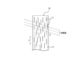
- FIG. 1 schematically shows a cross-sectional state in the thickness direction of the electromagnetic wave absorbing heat conducting sheet of the present invention. As shown in FIG. 1, in the electromagnetic wave absorption heat conductive sheet 1 of the present invention, the fibrous heat conductive filler 12 is oriented in one direction (direction X in FIG. 1).
- the fibrous thermal conductive filler 12 As shown in FIG. 1, by orienting the fibrous thermal conductive filler 12, in the electromagnetic wave absorbing thermal conductive sheet 1, the fibrous thermal conductive filler 12 is regularly arranged, The magnetic metal powder 13 is regularly and uniformly dispersed. As a result, the effects of the fibrous thermal conductive filler 12 and the magnetic metal powder 13 can be more efficiently exhibited, so that thermal conductivity and electromagnetic wave absorption can be achieved at a high level.
- the “fibrous” of the fibrous thermal conductive filler in the present invention means a shape having a high aspect ratio (approximately 6 or more). Therefore, in the present invention, not only thermal conductive fillers such as fibers and rods, but also granular fillers having a high aspect ratio, flaky thermal conductive fillers, and the like are used as fibrous thermal conductive fillers. included.
- the type of the fibrous thermally conductive filler is not particularly limited as long as it is a fibrous and highly thermally conductive material.
- metals such as silver, copper, and aluminum, alumina, and nitriding Examples thereof include ceramics such as aluminum, silicon carbide, and graphite, and carbon fibers.
- these fibrous thermal conductive fillers it is preferable to use carbon fibers from the viewpoint of obtaining higher thermal conductivity.
- about the said heat conductive filler you may use individually by 1 type, and may mix and use 2 or more types.
- both of them may be fibrous thermal conductive fillers, or the thermal conductivity of a different shape from the fibrous thermal conductive fillers. You may mix and use a filler.
- the type of the carbon fiber is not particularly limited and can be appropriately selected depending on the purpose.
- pitch-based, PAN-based, PBO fiber graphitized, synthesized by arc discharge method, laser evaporation method, CVD method (chemical vapor deposition method), CCVD method (saw medium chemical vapor deposition method), etc. Things can be used.
- carbon fibers obtained by graphitizing PBO fibers and pitch-based carbon fibers are more preferable because high thermal conductivity can be obtained.
- the carbon fiber can be used after partly or entirely treating the carbon fiber, if necessary.
- the surface treatment include oxidation treatment, nitriding treatment, nitration, sulfonation, or attaching a metal, a metal compound, an organic compound, or the like to the surface of a functional group or carbon fiber introduced to the surface by these treatments.
- the process etc. which are combined are mentioned.
- the functional group include a hydroxyl group, a carboxyl group, a carbonyl group, a nitro group, and an amino group.
- the average fiber length (average major axis length) of the carbon fiber is not particularly limited and may be appropriately selected. However, from the viewpoint of surely obtaining high thermal conductivity, it is in the range of 50 ⁇ m to 300 ⁇ m. Is more preferable, and the range of 75 ⁇ m to 275 ⁇ m is more preferable, and the range of 90 ⁇ m to 250 ⁇ m is particularly preferable. Furthermore, the average fiber diameter (average minor axis length) of the carbon fiber is not particularly limited and may be appropriately selected. However, it is in the range of 4 ⁇ m to 20 ⁇ m from the viewpoint of surely obtaining high thermal conductivity. Preferably, the range is from 5 ⁇ m to 14 ⁇ m.
- the aspect ratio (average major axis length / average minor axis length) of the carbon fiber is preferably 6 or more, more preferably 7 to 30 from the viewpoint of surely obtaining high thermal conductivity. . Even when the aspect ratio is small, an effect of improving thermal conductivity or the like can be seen, but an aspect ratio is preferably 6 or more because a large effect of improving characteristics cannot be obtained due to a decrease in orientation. On the other hand, when it exceeds 30, the dispersibility in the electromagnetic wave absorbing heat conductive sheet is lowered, so that there is a possibility that sufficient heat conductivity cannot be obtained.
- the average major axis length and the average minor axis length of the carbon fiber can be measured by, for example, a microscope, a scanning electron microscope (SEM), and the like, and the average can be calculated from a plurality of samples.
- the content of the fibrous heat conductive filler in the electromagnetic wave absorbing heat conductive sheet is not particularly limited and may be appropriately selected depending on the intended purpose, but is 4 vol% to 40 vol%. It is preferably 5% by volume to 30% by volume, more preferably 6% by volume to 20% by volume. If the content is less than 4% by volume, it may be difficult to obtain a sufficiently low heat resistance. If the content exceeds 40% by volume, the moldability of the heat conductive sheet and the fibrous heat conduction may be obtained. This may affect the orientation of the conductive filler.
- the said fibrous heat conductive filler 12 has orientated, and the orientation direction X is the extension direction L of the sheet
- the orientation direction X is the extension direction L of the sheet
- the heat conducting property and / or electromagnetic wave absorbing property of the electromagnetic wave absorbing heat conducting sheet 1 of the present invention can be realized at a higher level.
- the extending direction L of the sheet surface is a direction in which the surface of the electromagnetic wave absorbing heat conductive sheet 1 extends as the name suggests, and the electromagnetic wave absorbing heat conductive sheet was cut out from a sheet-shaped body to be described later.
- orientation direction X of each fibrous thermal conductive filler 12 does not need to be completely coincident. In the present invention, if the orientation direction X is within ⁇ 10 °, the orientation direction X is oriented in one direction. It can be said that.
- the orientation direction X of the fibrous thermally conductive filler 12 is in a range of 60 ° to 90 ° with respect to the extending direction L of the sheet surface (angle ⁇ : a range of 60 ° to 90 °). It is preferable from the point which can improve thermal conductivity more greatly.
- the orientation direction X of the fibrous thermally conductive filler 12 is in the range of more than 60 ° to 90 ° with respect to the extending direction L of the sheet surface
- the heat in the thickness direction of the electromagnetic wave absorbing heat conductive sheet Conductivity is 5 W / (m ⁇ K) or more
- transmission absorption at 3 GHz is 30% or more
- transmission absorption at 6 GHz is 70% or more.
- the transmission absorptance is a value measured by a microstrip line method using an electromagnetic wave absorbing heat conductive sheet having a thickness of 1 mm cut out in a disk shape of ⁇ 20 mm.
- the orientation direction X of the fibrous heat conductive filler 12 is in a range of 30 ° to 60 ° with respect to the extending direction L of the sheet surface (angle ⁇ : a range of 30 ° to 60 °). It is preferable from the point that heat conductivity and electromagnetic wave absorbability can be improved in a well-balanced manner.
- the orientation direction X of the fibrous thermally conductive filler 12 is in the range of more than 30 ° to 60 ° with respect to the extending direction L of the sheet surface
- the heat in the thickness direction of the electromagnetic wave absorbing heat conductive sheet Conductivity is 2.7 W / (m ⁇ K) or more
- transmission absorption at 3 GHz is 39% or more
- transmission absorption at 6 GHz is 70% or more.
- the transmission absorptance is a value measured by a microstrip line method using an electromagnetic wave absorbing heat conductive sheet having a thickness of 1 mm cut out in a disk shape of ⁇ 20 mm.
- the orientation direction X of the fibrous thermally conductive filler 12 is in a range of 0 ° to 30 ° with respect to the extending direction L of the sheet surface (angle ⁇ : a range of 0 ° to 30 °). This is preferable because the electromagnetic wave absorbability can be greatly improved.
- the orientation direction X of the fibrous heat conductive filler 12 is in the range of 0 ° to 30 ° with respect to the extending direction L of the sheet surface, heat conduction in the thickness direction of the electromagnetic wave absorbing heat conductive sheet The rate is 1.5 W / (m ⁇ K) or more, the transmission absorption rate at 3 GHz is 68% or more, and the transmission absorption rate at 6 GHz is 70% or more.
- the thermal conductivity in the thickness direction is low, but since the thermal conductivity in the in-plane direction is high, it functions as a heat spreader.
- the transmission absorptance is a value measured by a microstrip line method using an electromagnetic wave absorbing heat conductive sheet having a thickness of 1 mm cut out in a disk shape of ⁇ 20 mm.
- the method of changing the orientation direction X of the fibrous heat conductive filler 12 will be described in detail in the description of the method for producing an electromagnetic wave absorbing heat conductive sheet of the present invention.
- the orientation direction X of the fibrous thermal conductive filler 12 can be adjusted by adjusting the cut-out angle in the original sheet molded body with the thermal conductive filler 12 oriented.
- the electromagnetic wave absorbing heat conductive sheet of the present invention preferably further contains an inorganic filler. This is because the heat conductivity of the electromagnetic wave absorbing heat conductive sheet can be further increased and the strength of the sheet can be improved.
- the inorganic filler is not particularly limited with respect to shape, material, average particle diameter, and the like, and can be appropriately selected according to the purpose. Examples of the shape include a spherical shape, an elliptical spherical shape, a lump shape, a granular shape, a flat shape, and a needle shape. Among these, spherical and elliptical shapes are preferable from the viewpoint of filling properties, and spherical shapes are particularly preferable.
- the inorganic filler material examples include aluminum nitride (aluminum nitride: AlN), silica, alumina (aluminum oxide), boron nitride, titania, glass, zinc oxide, silicon carbide, silicon (silicon), silicon oxide, and aluminum oxide. And metal particles. These may be used individually by 1 type and may use 2 or more types together. Among these, alumina, boron nitride, aluminum nitride, zinc oxide, and silica are preferable, and alumina and aluminum nitride are particularly preferable from the viewpoint of thermal conductivity.
- the inorganic filler may be a surface-treated one.
- the inorganic filler is treated with a coupling agent as the surface treatment, the dispersibility of the inorganic filler is improved and the flexibility of the heat conductive sheet is improved.
- the average particle diameter of the said inorganic filler can select suitably according to the kind etc. of an inorganic substance.
- the inorganic filler is alumina
- the average particle size is preferably 1 ⁇ m to 10 ⁇ m, more preferably 1 ⁇ m to 5 ⁇ m, and particularly preferably 4 ⁇ m to 5 ⁇ m.
- the average particle size is less than 1 ⁇ m, the viscosity increases and mixing may be difficult.
- the average particle size exceeds 10 ⁇ m, the thermal resistance of the heat conductive sheet may increase.
- the average particle diameter is preferably 0.3 ⁇ m to 6.0 ⁇ m, more preferably 0.3 ⁇ m to 2.0 ⁇ m, and particularly preferably 0.5 ⁇ m to 1.5 ⁇ m. preferable. If the average particle size is less than 0.3 ⁇ m, the viscosity may increase and mixing may be difficult, and if it exceeds 6.0 ⁇ m, the thermal resistance of the heat conductive sheet may increase.
- the average particle diameter of the said inorganic filler can be measured with a particle size distribution meter and a scanning electron microscope (SEM), for example.
- the magnetic metal powder contained in the electromagnetic wave absorbing heat conducting sheet of the present invention is a component for improving the electromagnetic wave absorbing property of the sheet.
- a well-known magnetic metal powder can be selected suitably.
- amorphous metal powder or crystalline metal powder can be used.
- amorphous metal powders include Fe-Si-B-Cr, Fe-Si-B, Co-Si-B, Co-Zr, Co-Nb, and Co-Ta.
- the crystalline metal powder examples include pure iron, Fe-based, Co-based, Ni-based, Fe-Ni-based, Fe-Co-based, Fe-Al-based, Fe-Si-based, and Fe-Si-Al-based. Fe-Ni-Si-Al-based materials and the like.
- the crystalline metal powder is a microcrystalline metal obtained by adding a small amount of N (nitrogen), C (carbon), O (oxygen), B (boron), etc. to the crystalline metal powder. Powder may be used.
- N nitrogen
- C carbon
- O oxygen
- B boron
- a magnetic metal powder having a particle size of several ⁇ m to several tens of ⁇ m and a spherical shape.
- a magnetic metal powder can be produced by, for example, an atomizing method or a method of thermally decomposing metal carbonyl.
- the atomizing method has the advantage that a spherical powder is easy to make.
- the molten metal flows out from the nozzle, and a jet stream of air, water, inert gas, etc. is sprayed on the molten metal and solidified as droplets. It is a method of making a powder.
- the cooling rate is preferably about 10 6 (K / s) in order to prevent the molten metal from crystallizing.
- the surface of the amorphous alloy powder can be made smooth.
- a filling property can be improved with respect to binder resin.
- the filling property can be further improved by performing the coupling treatment.
- the electromagnetic wave absorbing heat conductive sheet of the present invention may contain other components as appropriate in addition to the polymer matrix component, fibrous heat conductive filler, inorganic filler and magnetic metal powder described above.
- other components include a thixotropic agent, a dispersant, a curing accelerator, a retarder, a slightly tackifier, a plasticizer, a flame retardant, an antioxidant, a stabilizer, and a colorant.
- the thickness of the electromagnetic wave absorbing heat conductive sheet of the present invention is not particularly limited and can be appropriately changed depending on the place where the sheet is used. For example, considering the adhesiveness and strength of the sheet, the thickness is in the range of 0.2 mm to 5 mm. can do.
- the method for producing an electromagnetic wave absorbing heat conductive sheet of the present invention comprises a step of preparing a composition for a sheet comprising a polymer matrix component, a fibrous heat conductive filler, and a magnetic metal powder (sheet composition preparing step).
- a step of orienting the fibrous thermally conductive filler (filler orientation step); In a state where the orientation of the fibrous heat conductive filler is maintained, the polymer matrix component is cured to produce a sheet molded body (sheet molded body producing process); A step of cutting the sheet molded body so as to form an angle of 0 ° to 90 ° with respect to the long axis direction of the oriented fibrous heat conductive filler to produce an electromagnetic wave absorbing heat conductive sheet ( Electromagnetic wave absorbing heat conductive sheet manufacturing process), It is characterized by including. By passing through each said process, the electromagnetic wave absorption heat conductive sheet of this invention can be obtained. About the obtained electromagnetic wave absorption heat conductive sheet, as above-mentioned, it is excellent in thermal conductivity and electromagnetic wave absorptivity.
- the manufacturing method of the electromagnetic wave absorption heat conductive sheet of this invention includes the composition preparation process for sheets.
- this sheet composition preparation step the above-described polymer matrix component, fibrous thermal conductive filler and magnetic metal powder, and further, an inorganic filler and / or other components are blended to prepare a sheet composition.
- the procedure for blending and preparing each component is not particularly limited.
- the polymer matrix component includes a polymer matrix component, a fibrous thermal conductive filler, an inorganic filler, a magnetic metal powder, and other components. Is added and mixed to prepare a sheet composition.
- the manufacturing method of the electromagnetic wave absorption heat conductive sheet of this invention includes the composition preparation process for sheets.
- the method for orienting the fibrous heat conductive filler is not particularly limited as long as it is a means capable of orienting in one direction.
- the fibrous thermally conductive filler As a method for orienting the fibrous thermally conductive filler in one direction, it may be performed by extruding or press-fitting the sheet composition under a high shear force into a hollow mold. It is done. By this method, the fibrous heat conductive filler can be oriented relatively easily, and the orientation of the fibrous heat conductive filler is the same (within ⁇ 10 °).
- Specific examples of the method for extruding or press-fitting the sheet composition into the hollow mold described above under a high shear force include an extrusion molding method and a mold molding method.
- the binder resin flows, and its flow direction
- the carbon fibers are oriented along. At this time, if a slit is attached to the tip of the die, the carbon fibers are more easily oriented.
- the size and shape of the molded body can be determined according to the required size of the electromagnetic wave absorbing heat conductive sheet. For example, a rectangular parallelepiped having a vertical size of 0.5 cm to 15 cm and a horizontal size of 0.5 cm to 15 cm can be mentioned. The length of the rectangular parallelepiped may be determined as necessary.
- the manufacturing method of the electromagnetic wave absorption heat conductive sheet of this invention includes the molded object preparation process for sheets.
- the said molded object for sheets means the sheet
- the molded body for the sheet is produced by curing the polymer matrix component while maintaining the orientation state of the fibrous thermal conductive filler performed in the filler orientation step described above.
- the method and conditions for curing the polymer matrix component can be changed according to the type of the polymer matrix component.
- the curing temperature in thermosetting can be adjusted.
- the thermosetting resin contains a main component of a liquid silicone gel and a curing agent
- curing is preferably performed at a curing temperature of 80 ° C. to 120 ° C.
- the curing time in thermosetting is not particularly limited, but can be 1 hour to 10 hours.
- the manufacturing method of the electromagnetic wave absorption heat conductive sheet of this invention includes an electromagnetic wave absorption heat conductive sheet preparation process.
- the angle ⁇ is 0 ° to 90 ° with respect to the long axis direction J of the oriented fibrous heat conductive filler 12.
- the sheet molded body is cut.
- the sheet molded body 10 obtained in the sheet molded body manufacturing step is in a state in which the major axis of the fibrous thermal conductive filler 12 is oriented in a certain direction J.
- FIG. 2 shows a state in which the metal magnetic powder 13 is omitted for easy viewing.
- the electromagnetic wave absorbing heat conducting sheet 1 shown in FIG. 1 can be obtained by cutting into a sheet shape with a constant cutting angle ⁇ with respect to the major axis direction J of the carbon fiber 12.
- the cut surface of the sheet molded body 10 in FIG. 2 is the sheet surface in FIG.
- the cutting angle ⁇ with respect to the major axis direction J of the carbon fiber 12 depending on the orientation direction X of the carbon fiber 12 in the obtained electromagnetic wave absorbing heat conductive sheet 1 (angle ⁇ with respect to the extending direction of the sheet surface), It can be adjusted appropriately.
- the major axis direction J of the carbon fiber 12 The cutting angle ⁇ with respect to the angle may be 30 °.
- the slicing device is not particularly limited as long as it is a means capable of cutting the sheet molded body, and a known slicing device can be appropriately used.
- a known slicing device can be appropriately used.
- an ultrasonic cutter, a planer ( ⁇ ), or the like can be used.
- the method for producing an electromagnetic wave absorbing heat conductive sheet of the present invention further includes smoothing the surface of the electromagnetic wave absorbing heat conductive sheet, increasing the adhesion, and reducing the interfacial contact resistance at light loads.
- a step of pressing can be included.
- the said press it can carry out using a pair of press apparatus which consists of a flat board and a press head with the flat surface, for example. Moreover, you may press using a pinch roll.
- the pressure at the time of pressing is not particularly limited and can be appropriately selected according to the purpose. However, if it is too low, the thermal resistance tends to be the same as when not pressing, and if it is too high, the sheet is stretched. Due to the tendency, the pressure range is preferably 0.1 MPa to 100 MPa, and more preferably 0.5 MPa to 95 MPa.
- the semiconductor device of the present invention is a semiconductor device comprising a heat source, a heat radiating member, and an electromagnetic wave absorbing heat conductive sheet sandwiched between the heat source and the heat radiating member, wherein the electromagnetic wave absorbing heat conductive sheet is described above. It is an electromagnetic wave absorption heat conductive sheet of the present invention. By using the electromagnetic wave absorbing heat conductive sheet of the present invention, the obtained semiconductor device is excellent in electromagnetic wave suppression effect while having high heat dissipation.
- the heat source is not particularly limited as long as it generates heat in the semiconductor device.
- an electronic part etc. are mentioned,
- CPU, MPU, a graphic arithmetic element, an image sensor etc. are mentioned.
- the heat radiating member conducts heat generated from the heat source and dissipates it to the outside.
- a radiator, a cooler, a heat sink, a heat spreader, a die pad, a printed board, a cooling fan, a Peltier element, a heat pipe, a metal cover, a housing, and the like can be given.
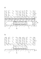
- FIG. 3A is a schematic cross-sectional view showing an example of the semiconductor device of the present invention.
- the semiconductor device includes an electromagnetic wave absorbing heat conductive sheet 1, a heat spreader 2, an electronic component 3, a heat sink 5, and a wiring substrate 6.
- the electromagnetic wave absorbing heat conducting sheet 1 absorbs unnecessary electromagnetic waves generated in the electronic component 3 and electromagnetic waves radiated from other components and dissipates heat generated by the electronic component 3, as shown in FIG.
- the heat spreader 2 is fixed to the main surface 2 a facing the electronic component 3 and is sandwiched between the electronic component 3 and the heat spreader 2. Further, the electromagnetic wave absorbing heat conducting sheet 1 is sandwiched between the heat spreader 2 and the heat sink 5.
- the heat spreader 2 is formed in, for example, a rectangular plate shape, and has a main surface 2a facing the electronic component 3 and a side wall 2b erected along the outer periphery of the main surface 2a.
- the heat spreader 2 is provided with the electromagnetic wave absorbing heat conductive sheet 1 on the main surface 2a surrounded by the side wall 2b, and the heat sink 5 is provided on the other surface 2c opposite to the main surface 2a via the electromagnetic wave absorbing heat conductive sheet 1. It is done.
- the heat spreader 2 has a higher thermal conductivity, so that the thermal resistance is reduced and the heat of the electronic component 3 such as a semiconductor element is efficiently absorbed. Therefore, the heat spreader 2 is formed using, for example, copper or aluminum having good thermal conductivity. be able to.
- the electronic component 3 is a semiconductor package such as BGA, for example, and is mounted on the wiring board 6. Further, the heat spreader 2 also has the front end surface of the side wall 2b mounted on the wiring board 6, and thereby surrounds the electronic component 3 at a predetermined distance by the side wall 2b.
- the electromagnetic wave absorbing heat conductive sheet 1 is adhered to the main surface 2 a of the heat spreader 2, so that the heat generated by the electronic component 3 is absorbed and radiated from the heat sink 5.
- the adhesion between the heat spreader 2 and the electromagnetic wave absorbing heat conducting sheet 1 can be performed by the adhesive force of the electromagnetic wave absorbing heat conducting sheet 1 itself.
- FIG. 3B is a schematic cross-sectional view showing another example of the semiconductor device of the present invention.
- the semiconductor device includes an electromagnetic wave absorbing heat conductive sheet 1, a heat spreader 2, an electronic component 3, a heat sink 5, and a wiring substrate 6.
- the electromagnetic wave absorbing heat conducting sheet 1 absorbs unnecessary electromagnetic waves generated in the electronic component 3 and electromagnetic waves radiated from other components, and dissipates heat generated by the electronic component 3, as shown in FIG. As shown, the electronic component 3 is fixed to the upper surface 3 a and is sandwiched between the electronic component 3 and the heat spreader 2.
- the two-component addition reaction type liquid silicone is obtained by mixing a silicone A liquid (main agent) and a silicone B liquid (curing agent) in a ratio of 19:16.
- the obtained silicone composition was extruded into a rectangular parallelepiped mold 30 mm ⁇ 30 mm in which a peeled PET film was attached to the inner wall to mold a silicone molded body.
- the obtained silicone molded body was cured in an oven at 100 ° C. for 6 hours to obtain a cured silicone (sheet molded body).
- the obtained cured silicone was cut with an ultrasonic cutter perpendicular to the long axis of the oriented carbon fiber, that is, with a cutting angle ⁇ : 90 ° (orientation angle ⁇ : 90 °), and the thickness was 1 mm.
- a sample of an electromagnetic wave absorbing heat conductive sheet was obtained.
- the slice speed of the ultrasonic cutter was 50 mm per second.
- the ultrasonic vibration applied to the ultrasonic cutter had an oscillation frequency of 20.5 kHz and an amplitude of 60 ⁇ m.
- Example 2 In Example 2, the cured silicone product was cut at a cutting angle ⁇ : 75 ° (orientation angle ⁇ : 75 °) to obtain a sample of an electromagnetic wave absorbing heat conductive sheet having a thickness of 1 mm.
- the blending and other steps are the same as in Example 1.
- Example 3 the cured silicone product was cut at a cutting angle ⁇ : 60 ° (orientation angle ⁇ : 60 °) to obtain a sample of an electromagnetic wave absorbing heat conductive sheet having a thickness of 1 mm.
- the blending and other steps are the same as in Example 1.
- Example 4 the cured silicone product was cut at a cutting angle ⁇ : 45 ° (orientation angle ⁇ : 45 °) to obtain a sample of an electromagnetic wave absorbing heat conductive sheet having a thickness of 1 mm.
- the blending and other steps are the same as in Example 1.
- Example 5 (Example 5) In Example 5, the above silicone cured product was cut at a cutting angle ⁇ : 30 ° (orientation angle ⁇ : 30 °) to obtain a sample of an electromagnetic wave absorbing heat conductive sheet having a thickness of 1 mm. The blending and other steps are the same as in Example 1.
- Example 6 the cured silicone product was cut at a cutting angle ⁇ : 15 ° (orientation angle ⁇ : 15 °) to obtain a sample of an electromagnetic wave absorbing heat conductive sheet having a thickness of 1 mm.
- the blending and other steps are the same as in Example 1.
- the blending and other steps are the same as in Example 1.
- Comparative Example 1 the cured silicone was cut at a cutting angle of 90 ° (orientation angle ⁇ : 90 °) to obtain a sample of an electromagnetic wave absorbing heat conductive sheet having a thickness of 1 mm.
- Comparative Example 2 In Comparative Example 2, the cured silicone product was cut at a cutting angle of 45 ° (orientation angle ⁇ : 45 °) to obtain a sample of an electromagnetic wave absorbing heat conductive sheet having a thickness of 1 mm.
- Comparative Example 3 (Comparative Example 3)
- the silicone cured product was cut at a cutting angle of 0 ° (orientation angle ⁇ : 0 °) to obtain a sample of an electromagnetic wave absorbing heat conductive sheet having a thickness of 1 mm.
- a silicone composition (sheet composition) was prepared by dispersing to 12 vol%. The other steps are the same as in Example 1.
- Comparative Example 4 the silicone cured product was cut at a cutting angle of 0 ° (orientation angle ⁇ : 0 °) to obtain a sample of an electromagnetic wave absorbing heat conductive sheet having a thickness of 1 mm.
- a silicone composition (sheet composition) was prepared. The other steps are the same as in Example 1.
- Comparative Example 5 Comparative Example 5
- the silicone molded body was not molded by being extruded into a mold. Therefore, the carbon fiber in the obtained electromagnetic wave absorption heat conductive sheet is not oriented in one direction.
- the other steps are the same as in Example 1.
- Comparative Example 6 (Comparative Example 6)
- the silicone molded body was not molded by being extruded into a mold. Therefore, the carbon fiber in the obtained electromagnetic wave absorption heat conductive sheet is not oriented in one direction.
- the other steps are the same as in Example 1.
- Example 8 to 11 In Examples 8 to 11, the above cured silicone was cut at a cutting angle of 90 ° (orientation angle ⁇ : 90 °) to obtain a sample of an electromagnetic wave absorbing heat conductive sheet having a thickness of 1 mm.
- the composition is in a volume ratio such that two-component addition reaction type liquid silicone: amorphous magnetic particles: pitch-based carbon fiber has a ratio as shown in Table 2. The other steps are the same as in Example 1.
- Example 12 to 15 In Examples 12 to 15, the above cured silicone was cut at a cutting angle of 45 ° (orientation angle ⁇ : 45 °) to obtain a sample of an electromagnetic wave absorbing heat conductive sheet having a thickness of 1 mm.
- the composition is in a volume ratio such that two-component addition reaction type liquid silicone: amorphous magnetic particles: pitch-based carbon fiber has a ratio as shown in Table 2. The other steps are the same as in Example 1.
- Example 16 to 19 the cured silicone product was cut at a cutting angle of 0 ° (orientation angle ⁇ : 0 °) to obtain a sample of an electromagnetic wave absorbing heat conductive sheet having a thickness of 1 mm.
- the composition is in a volume ratio such that two-component addition reaction type liquid silicone: amorphous magnetic particles: pitch-based carbon fiber has a ratio as shown in Table 2. The other steps are the same as in Example 1.
- the microstrip line method described in IEC62333-2 was used.
- the measurement system 100 uses the one shown in FIG. 7 and measures the reflected signal (S11) and the transmitted signal (S21) by the network analyzer 110.
- the microstrip line 112 is formed on the surface of a 100 ⁇ 100 ⁇ 1.6 mm dielectric substrate (backside copper) with a width of 4 mm, and is adjusted to have a characteristic impedance of 50 ⁇ .
- Each sample 111 was cut out into a disk shape of ⁇ 20 mm, attached to the center of the microstrip line, S11 and S21 were measured, and the absorption rate was calculated.
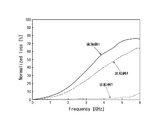
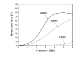
- the thermal conductivity is as high as 6 W / (m ⁇ K) or more, and the transmission absorption rate is 35% or more especially in the 3 GHz band, and 76% or more in the 6 GHz band. Excellent characteristics in high frequency range.
- the thermal conductivity is relatively high at 3.8 W / (m ⁇ K) or higher, and the transmission absorption rate is about 40% or higher in the 3 GHz band and 75% or higher in the 6 GHz band, which is a slightly low frequency range. The characteristics are improved.
- Example 5 to 7 although the thermal conductivity is a little lower, 2.7 to 1.5 W / (m ⁇ K), the transmission absorptivity is less than 5% even in the 1 GHz band, and less than 70% in the higher frequency range than the 3 GHz band. It was found that it exhibits particularly excellent characteristics. As described above, in Examples 1 to 7, excellent thermal conductivity and transmission absorptance can be obtained, and furthermore, an appropriate balance between the thermal conductivity and the transmission absorptivity can be set by the orientation angle of the carbon fiber. all right. On the other hand, looking at the comparative example, in Comparative Examples 1 and 2, which are composed of only carbon fibers and silica without containing a magnetic material, the transmission absorptance is remarkably small.
- Table 2 shows the characteristic values of thermal conductivity and transmission absorptivity when the content ratio of carbon fiber and magnetic material is changed at carbon fiber orientation angles of 90 °, 45 °, and 0 °. It was found that by adjusting the content ratio of the carbon fiber and the magnetic material together with the orientation angle of the fiber, various characteristic values of thermal conductivity and transmission absorption rate can be set.
- an electromagnetic wave absorbing heat conductive sheet having excellent heat conductivity and electromagnetic wave absorbability, and a method for producing the same. Moreover, it becomes possible to provide the semiconductor device excellent in heat dissipation and electromagnetic wave suppression using this electromagnetic wave absorption heat conductive sheet.
- Electromagnetic wave absorption heat conductive sheet 2 Heat spreader 2a Main surface 2b Side wall 2c Other surface 3 Electronic component 3a Upper surface 5 Heat sink 6 Wiring board 10 Electromagnetic wave absorption heat conductive sheet 11 Polymer matrix component 12 Carbon fiber 13 Magnetic metal powder 100 Measurement system 110 Network Analyzer 111 Electromagnetic wave absorbing heat conductive sheet sample 112 Microstrip line
Landscapes
- Engineering & Computer Science (AREA)
- Microelectronics & Electronic Packaging (AREA)
- Physics & Mathematics (AREA)
- Electromagnetism (AREA)
- Thermal Sciences (AREA)
- Textile Engineering (AREA)
- Shielding Devices Or Components To Electric Or Magnetic Fields (AREA)
- Cooling Or The Like Of Semiconductors Or Solid State Devices (AREA)
- Chemical & Material Sciences (AREA)
- Materials Engineering (AREA)
- Cooling Or The Like Of Electrical Apparatus (AREA)
- Health & Medical Sciences (AREA)
- Toxicology (AREA)
Abstract
優れた熱伝導性及び電磁波吸収性を有する、電磁波吸収熱伝導シートを提供する。 上記課題を解決するべく、本発明の電磁波吸収熱伝導シートは、高分子マトリックス成分と、磁性金属粉と、一方向に配向している繊維状の熱伝導性充填剤とを含むことを特徴とする。
Description
本発明は、優れた熱伝導性及び電磁波吸収性を有する、電磁波吸収熱伝導シート、電磁波吸収熱伝導シートの製造方法及び半導体装置に関するものである。
近年、電子機器は、小型化の傾向をたどる一方、アプリケーションの多様性のために電力消費量をそれほど変化させることができないため、機器内における放熱対策がより一層重要視されている。
上述した電子機器における放熱対策として、銅やアルミ等といった熱伝導率の高い金属材料で作製された放熱板やヒートパイプ、あるいはヒートシンク等が広く利用されている。これらの熱伝導性に優れた放熱部品は、放熱効果又は機器内の温度緩和を図るため、電子機器内における発熱部である半導体パッケージ等の電子部品に近接するようにして配置される。また、これらの熱伝導性に優れた放熱部品は、発熱部である電子部品から低温の場所へ亘って配置される。
ただし、電子機器内における発熱部は、電流密度が高い半導体素子等の電子部品であり、電流密度が高いということは、不要輻射の成分となり得る電界強度又は磁界強度が大きいことが考えられる。このため、金属で作製された放熱部品を電子部品の近辺に配置すると、熱の吸収を行うとともに、電子部品内を流れる電気信号の高調波成分をも拾ってしまうという問題があった。具体的には、放熱部品が金属材料で作製されているため、それ自体が高調波成分のアンテナとして機能したり、高調波ノイズ成分の伝達経路として働いてしまうような場合である。
そのような問題を解決するべく、熱伝導性シートに、磁界のカップリングを断ち切るために、磁性材料を含有するもの技術が開発されている。
例えば特許文献1には、CPU等の半導体とヒートシンクに挟んで用いる電磁吸収熱伝導シートであって、シリコーンに軟磁性粉末と熱伝導フィラーを混ぜることによって、軟磁性粉末の磁気吸収効果と、熱伝導フィラーの熱伝導特性で電磁波吸収と熱伝導特性の両立を図る、という技術が開示されている。
しかしながら、特許文献1の技術では、電磁波吸収効果について一定の効果はみられるものの、シートの垂直方向に対する熱伝導率が1.5W/(m・K)程度であり、近年の放熱に対する要求に対しては十分な特性とはなっていない。
例えば特許文献1には、CPU等の半導体とヒートシンクに挟んで用いる電磁吸収熱伝導シートであって、シリコーンに軟磁性粉末と熱伝導フィラーを混ぜることによって、軟磁性粉末の磁気吸収効果と、熱伝導フィラーの熱伝導特性で電磁波吸収と熱伝導特性の両立を図る、という技術が開示されている。
しかしながら、特許文献1の技術では、電磁波吸収効果について一定の効果はみられるものの、シートの垂直方向に対する熱伝導率が1.5W/(m・K)程度であり、近年の放熱に対する要求に対しては十分な特性とはなっていない。
また、特許文献2には、繊維状導電性カーボンとカルボニル鉄を含んだ電磁波干渉抑制シートであって、繊維状導電性カーボンとカルボニル鉄との体積比率を3~10:50~70とすることでシート強度、柔軟性を確保しつつ電磁波吸収量を増やす、という技術が開示されている。
しかしながら、特許文献2の技術では、繊維状導電性カーボンが10体積%を超えると、分散が不良となり均一なシートが得られなくなるという問題があり、熱伝導性に関しては十分な考慮がされていなかった。
しかしながら、特許文献2の技術では、繊維状導電性カーボンが10体積%を超えると、分散が不良となり均一なシートが得られなくなるという問題があり、熱伝導性に関しては十分な考慮がされていなかった。
さらに、特許文献3には、樹脂マトリックス中に、炭素繊維と磁性粉とを含んだ電磁波干渉抑制シートを用いることで、電磁ノイズの抑制及び熱伝導率の向上を図る技術が開示されている。
しかしながら、特許文献3の技術では、良好な熱伝導性が得られるものの、電磁ノイズの抑制という点では十分な効果が得られておらず、実用化の点を考慮するとさらなる改良を図ることが望まれていた。
しかしながら、特許文献3の技術では、良好な熱伝導性が得られるものの、電磁ノイズの抑制という点では十分な効果が得られておらず、実用化の点を考慮するとさらなる改良を図ることが望まれていた。
本発明は、かかる事情に鑑みてなされたものであって、優れた熱伝導性及び電磁波吸収性を有する、電磁波吸収熱伝導シート及びその製造方法を提供することを目的とする。また、本発明の他の目的は、かかる電磁波吸収熱伝導シートを用い、放熱性及び電磁波抑制に優れた半導体装置を提供することを目的とする。
本発明者らは、上記の課題を解決するべく鋭意研究を重ねた結果、高分子マトリックス成分と、繊維状の熱伝導性充填剤と、磁性金属粉とを含み、該繊維状の熱伝導性充填剤を一方向に配向させるとともに、配向する方向を調整することによって、従来に比べて高いレベルで熱伝導性及び電磁波吸収性を両立できることを見出した。
本発明は、上記知見に基づきなされたものであり、その要旨は以下の通りである。
(1)高分子マトリックス成分と、磁性金属粉と、一方向に配向している繊維状の熱伝導性充填剤とを含むことを特徴とする、電磁波吸収熱伝導シート。
上記構成によって、優れた熱伝導性及び電磁波吸収性を実現できる。
(2)前記繊維状の熱伝導性充填剤の配向方向が、シート面の延在方向に対して60°超え~90°の範囲であることを特徴とする、上記(1)に記載の電磁波吸収熱伝導シート。
(3)前記電磁波吸収熱伝導シートの、厚さ方向の熱伝導率が5W/(m・K)以上、3GHzでの伝送吸収率が30%以上、6GHzでの伝送吸収率が70%以上であることを特徴とする、上記(1)に記載の電磁波吸収熱伝導シート。
(4)前記繊維状の熱伝導性充填剤の配向方向が、シート面の延在方向に対して30°超え~60°の範囲であることを特徴とする、上記(1)に記載の電磁波吸収熱伝導シート。
(5)前記電磁波吸収熱伝導シートの、厚さ方向の熱伝導率が2.7W/(m・K)以上、3GHzでの伝送吸収率が39%以上、6GHzでの伝送吸収率が70%以上であることを特徴とする、上記(4)に記載の電磁波吸収熱伝導シート。
(6)前記繊維状の熱伝導性充填剤の配向方向が、シート面の延在方向に対して0°~30°の範囲であることを特徴とする、上記(1)に記載の電磁波吸収熱伝導シート。
(7)前記電磁波吸収熱伝導シートの、厚さ方向の熱伝導率が1.5W/(m・K)以上、3GHzでの伝送吸収率が68%以上、6GHzでの伝送吸収率が70%以上であることを特徴とする、上記(6)に記載の電磁波吸収熱伝導シート。
(8)前記繊維状の熱伝導性充填剤の含有量が4~40体積%、前記磁性金属粉の含有量が35~75体積%であることを特徴とする、前記(1)~(7)のいずれかに記載の電磁波吸収熱伝導シート。
(9)前記繊維状の熱伝導性充填剤の含有量が5~30体積%、前記磁性金属粉の含有量が40~65体積%であることを特徴とする、上記(8)に記載の電磁波吸収熱伝導シート。
(10)前記繊維状の熱伝導性充填剤が、炭素繊維であることを特徴とする、前記(1)~(9)のいずれかに記載の電磁波吸収熱伝導シート。
(11)前記電磁波吸収熱伝導シートが、無機物フィラーをさらに含むことを特徴とする、前記(1)~(10)のいずれかに記載の電磁波吸収熱伝導シート。
(12)高分子マトリックス成分と、繊維状の熱伝導性充填剤と、磁性金属粉とを含むシート用組成物を調製する工程と、
前記繊維状の熱伝導性充填剤を配向させる工程と、
前記繊維状の熱伝導性充填剤の配向を維持した状態で、前記高分子マトリックス成分を硬化させて、シート用成形体を作製する工程と、
前記配向した繊維状の熱伝導性充填剤の長軸方向に対して、0°~90°の角度となるように、前記シート用成形体を切断し、電磁波吸収熱伝導シートを作製する工程と、
を含むことを特徴とする、電磁波吸収熱伝導シートの製造方法。
上記構成によって、優れた熱伝導性及び電磁波吸収性を有する電磁波吸収熱伝導シートを提供できる。
(13)前記繊維状の熱伝導性充填剤を配向させる工程が、中空状の型内に、前記シート用組成物を、高剪断力下で押し出すこと又は圧入することによって行われ、
前記シート用成形体を作製する工程が、前記高分子マトリックス成分を熱硬化させることによって行われることを特徴とする、上記(12)に記載の電磁波吸収熱伝導シートの製造方法。
(14)熱源と、放熱部材と、該熱源と該放熱部材との間に挟持された電磁波吸収熱伝導シートを備える半導体装置であって、
前記電磁波吸収熱伝導シートが、請求項1~11のいずれか1項に記載の電磁波吸収熱伝導シートであることを特徴とする、半導体装置。
上記構成によって、優れた放熱性及び電磁波抑制を実現できる。
(1)高分子マトリックス成分と、磁性金属粉と、一方向に配向している繊維状の熱伝導性充填剤とを含むことを特徴とする、電磁波吸収熱伝導シート。
上記構成によって、優れた熱伝導性及び電磁波吸収性を実現できる。
(2)前記繊維状の熱伝導性充填剤の配向方向が、シート面の延在方向に対して60°超え~90°の範囲であることを特徴とする、上記(1)に記載の電磁波吸収熱伝導シート。
(3)前記電磁波吸収熱伝導シートの、厚さ方向の熱伝導率が5W/(m・K)以上、3GHzでの伝送吸収率が30%以上、6GHzでの伝送吸収率が70%以上であることを特徴とする、上記(1)に記載の電磁波吸収熱伝導シート。
(4)前記繊維状の熱伝導性充填剤の配向方向が、シート面の延在方向に対して30°超え~60°の範囲であることを特徴とする、上記(1)に記載の電磁波吸収熱伝導シート。
(5)前記電磁波吸収熱伝導シートの、厚さ方向の熱伝導率が2.7W/(m・K)以上、3GHzでの伝送吸収率が39%以上、6GHzでの伝送吸収率が70%以上であることを特徴とする、上記(4)に記載の電磁波吸収熱伝導シート。
(6)前記繊維状の熱伝導性充填剤の配向方向が、シート面の延在方向に対して0°~30°の範囲であることを特徴とする、上記(1)に記載の電磁波吸収熱伝導シート。
(7)前記電磁波吸収熱伝導シートの、厚さ方向の熱伝導率が1.5W/(m・K)以上、3GHzでの伝送吸収率が68%以上、6GHzでの伝送吸収率が70%以上であることを特徴とする、上記(6)に記載の電磁波吸収熱伝導シート。
(8)前記繊維状の熱伝導性充填剤の含有量が4~40体積%、前記磁性金属粉の含有量が35~75体積%であることを特徴とする、前記(1)~(7)のいずれかに記載の電磁波吸収熱伝導シート。
(9)前記繊維状の熱伝導性充填剤の含有量が5~30体積%、前記磁性金属粉の含有量が40~65体積%であることを特徴とする、上記(8)に記載の電磁波吸収熱伝導シート。
(10)前記繊維状の熱伝導性充填剤が、炭素繊維であることを特徴とする、前記(1)~(9)のいずれかに記載の電磁波吸収熱伝導シート。
(11)前記電磁波吸収熱伝導シートが、無機物フィラーをさらに含むことを特徴とする、前記(1)~(10)のいずれかに記載の電磁波吸収熱伝導シート。
(12)高分子マトリックス成分と、繊維状の熱伝導性充填剤と、磁性金属粉とを含むシート用組成物を調製する工程と、
前記繊維状の熱伝導性充填剤を配向させる工程と、
前記繊維状の熱伝導性充填剤の配向を維持した状態で、前記高分子マトリックス成分を硬化させて、シート用成形体を作製する工程と、
前記配向した繊維状の熱伝導性充填剤の長軸方向に対して、0°~90°の角度となるように、前記シート用成形体を切断し、電磁波吸収熱伝導シートを作製する工程と、
を含むことを特徴とする、電磁波吸収熱伝導シートの製造方法。
上記構成によって、優れた熱伝導性及び電磁波吸収性を有する電磁波吸収熱伝導シートを提供できる。
(13)前記繊維状の熱伝導性充填剤を配向させる工程が、中空状の型内に、前記シート用組成物を、高剪断力下で押し出すこと又は圧入することによって行われ、
前記シート用成形体を作製する工程が、前記高分子マトリックス成分を熱硬化させることによって行われることを特徴とする、上記(12)に記載の電磁波吸収熱伝導シートの製造方法。
(14)熱源と、放熱部材と、該熱源と該放熱部材との間に挟持された電磁波吸収熱伝導シートを備える半導体装置であって、
前記電磁波吸収熱伝導シートが、請求項1~11のいずれか1項に記載の電磁波吸収熱伝導シートであることを特徴とする、半導体装置。
上記構成によって、優れた放熱性及び電磁波抑制を実現できる。
本発明によれば、優れた熱伝導性及び電磁波吸収性を有する、電磁波吸収熱伝導シート及びその製造方法を提供することが可能となる。また、かかる電磁波吸収熱伝導シートを用い、放熱性及び電磁波抑制に優れた半導体装置を提供することが可能となる。
以下、本発明の実施形態の一例を具体的に説明する。
<電磁波吸収熱伝導シート>
まず、本発明の電磁波吸収熱伝導シートについて説明する。
本発明は、高分子マトリックス成分と、繊維状の熱伝導性充填剤と、磁性金属粉とを含む、電磁波吸収熱伝導シートである。
<電磁波吸収熱伝導シート>
まず、本発明の電磁波吸収熱伝導シートについて説明する。
本発明は、高分子マトリックス成分と、繊維状の熱伝導性充填剤と、磁性金属粉とを含む、電磁波吸収熱伝導シートである。
(高分子マトリックス成分)
本発明の電磁波吸収熱伝導シートに含まれる高分子マトリックス成分は、電磁波吸収熱伝導シートの基材となる高分子成分のことである。その種類については、特に限定されず、公知の高分子マトリックス成分を適宜選択することができる。
例えば、高分子マトリックス成分の一つとして、熱硬化性ポリマーが挙げられる。
本発明の電磁波吸収熱伝導シートに含まれる高分子マトリックス成分は、電磁波吸収熱伝導シートの基材となる高分子成分のことである。その種類については、特に限定されず、公知の高分子マトリックス成分を適宜選択することができる。
例えば、高分子マトリックス成分の一つとして、熱硬化性ポリマーが挙げられる。
前記熱硬化性ポリマーとしては、例えば、架橋ゴム、エポキシ樹脂、ポリイミド樹脂、ビスマレイミド樹脂、ベンゾシクロブテン樹脂、フェノール樹脂、不飽和ポリエステル、ジアリルフタレート樹脂、シリコーン、ポリウレタン、ポリイミドシリコーン、熱硬化型ポリフェニレンエーテル、熱硬化型変性ポリフェニレンエーテル等が挙げられる。これらは、1種単独で使用してもよいし、2種以上を併用してもよい。
なお、前記架橋ゴムとしては、例えば、天然ゴム、ブタジエンゴム、イソプレンゴム、ニトリルゴム、水添ニトリルゴム、クロロプレンゴム、エチレンプロピレンゴム、塩素化ポリエチレン、クロロスルホン化ポリエチレン、ブチルゴム、ハロゲン化ブチルゴム、フッ素ゴム、ウレタンゴム、アクリルゴム、ポリイソブチレンゴム、シリコーンゴム等が挙げられる。これらは、1種単独で使用してもよいし、2種以上を併用してもよい。
また、これら熱硬化性ポリマーの中でも、成形加工性及び耐候性に優れるとともに、電子部品に対する密着性及び追従性の点から、シリコーンを用いることが好ましい。
前記シリコーンとしては、特に制限はなく、目的に応じてシリコーンの種類を適宜選択することができる。上述した成形加工性、耐候性、密着性等を得る観点からは、前記シリコーンとして、液状シリコーンゲルの主剤と、硬化剤とから構成されるシリコーンであることが好ましい。そのようなシリコーンとしては、例えば、付加反応型液状シリコーン、過酸化物を加硫に用いる熱加硫型ミラブルタイプのシリコーン等が挙げられる。これらの中でも、電子機器の放熱部材としては、電子部品の発熱面とヒートシンク面との密着性が要求されるため、付加反応型液状シリコーンが特に好ましい。
前記シリコーンとしては、特に制限はなく、目的に応じてシリコーンの種類を適宜選択することができる。上述した成形加工性、耐候性、密着性等を得る観点からは、前記シリコーンとして、液状シリコーンゲルの主剤と、硬化剤とから構成されるシリコーンであることが好ましい。そのようなシリコーンとしては、例えば、付加反応型液状シリコーン、過酸化物を加硫に用いる熱加硫型ミラブルタイプのシリコーン等が挙げられる。これらの中でも、電子機器の放熱部材としては、電子部品の発熱面とヒートシンク面との密着性が要求されるため、付加反応型液状シリコーンが特に好ましい。
前記付加反応型液状シリコーンとしては、ビニル基を有するポリオルガノシロキサンを主剤、Si-H基を有するポリオルガノシロキサンを硬化剤とした、2液性の付加反応型シリコーン等を用いることが好ましい。
なお、前記液状シリコーンゲルの主剤と、硬化剤との組合せにおいて、前記主剤と前記硬化剤との配合割合としては、質量比で、主剤:硬化剤=35:65~65:35であることが好ましい。
また、本発明の電磁波吸収熱伝導シートにおける前記高分子マトリックス成分の含有量は、特に制限されず、目的に応じて適宜選択することができるが、シートの成形加工性や、シートの密着性等を確保する観点からは、20体積%~50体積%程度であることが好ましく、30体積%~40体積%であることがより好ましい。
(熱伝導性充填剤)
本発明の電磁波吸収熱伝導シートに含まれる熱伝導性充填剤は、シートの熱伝導性を向上させるための成分である。熱伝導性充填剤の種類については、繊維状の熱伝導性充填剤であること以外は、特に限定されず、公知の熱伝導性充填剤を適宜選択することができる。
図1は、本発明の電磁波吸収熱伝導シートについて、厚さ方向の断面状態を模式的に示したものである。図1に示すように、本発明の電磁波吸収熱伝導シート1では、前記繊維状の熱伝導性充填剤12が、一方向(図1では方向X)に配向していることを特徴とする。
本発明の電磁波吸収熱伝導シートに含まれる熱伝導性充填剤は、シートの熱伝導性を向上させるための成分である。熱伝導性充填剤の種類については、繊維状の熱伝導性充填剤であること以外は、特に限定されず、公知の熱伝導性充填剤を適宜選択することができる。
図1は、本発明の電磁波吸収熱伝導シートについて、厚さ方向の断面状態を模式的に示したものである。図1に示すように、本発明の電磁波吸収熱伝導シート1では、前記繊維状の熱伝導性充填剤12が、一方向(図1では方向X)に配向していることを特徴とする。
図1に示すように、繊維状の熱伝導性充填剤12を配向させることによって、電磁波吸収熱伝導シート1において、繊維状の熱伝導性充填剤12が規則正しく配設されることに加えて、磁性金属粉13が、規則正しく均一に分散されることとなる。その結果、繊維状の熱伝導性充填剤12及び磁性金属粉13の効果が、より効率的に発揮できるため、熱伝導性及び電磁波吸収性を高いレベルで実現できる。
なお、本発明における前記繊維状の熱伝導性充填剤の「繊維状」とは、アスペクト比の高い(およそ6以上)の形状のことをいう。そのため、本発明では、繊維状や棒状等の熱導電性充填剤だけでなく、アスペクト比の高い粒状の充填材や、フレーク状の熱導電性充填剤等も繊維状の熱導電性充填剤に含まれる。
ここで、前記繊維状の熱伝導性充填剤の種類については、繊維状で且つ熱伝導性の高い材料であれば特に限定はされず、例えば、銀、銅、アルミニウム等の金属、アルミナ、窒化アルミニウム、炭化ケイ素、グラファイト等のセラミックス、炭素繊維等が挙げられる。
これらの繊維状の熱伝導性充填剤の中でも、より高い熱伝導性を得られる点からは、炭素繊維を用いることが好ましい。
なお、前記熱伝導性充填剤については、一種単独でもよいし、二種以上を混合して用いてもよい。また、二種以上の熱伝導性充填剤を用いる場合には、いずれも繊維状の熱伝導性充填剤であってもよいし、繊維状の熱伝導性充填剤と別の形状の熱伝導性充填剤とを混合して用いてもよい。
これらの繊維状の熱伝導性充填剤の中でも、より高い熱伝導性を得られる点からは、炭素繊維を用いることが好ましい。
なお、前記熱伝導性充填剤については、一種単独でもよいし、二種以上を混合して用いてもよい。また、二種以上の熱伝導性充填剤を用いる場合には、いずれも繊維状の熱伝導性充填剤であってもよいし、繊維状の熱伝導性充填剤と別の形状の熱伝導性充填剤とを混合して用いてもよい。
前記炭素繊維の種類について特に制限はなく、目的に応じて適宜選択することができる。例えば、ピッチ系、PAN系、PBO繊維を黒鉛化したもの、アーク放電法、レーザー蒸発法、CVD法(化学気相成長法)、CCVD法(沢媒化学気相成長法)等で合成されたものを用いることができる。これらの中でも、高い熱伝導性が得られる点から、PBO繊維を黒鉛化した炭素繊維、ピッチ系炭素繊維がより好ましい。
また、前記炭素繊維は、必要に応じて、その一部又は全部を表面処理して用いることができる。前記表面処理としては、例えば、酸化処理、窒化処理、ニトロ化、スルホン化、あるいはこれらの処理によって表面に導入された官能基若しくは炭素繊維の表面に、金属、金属化合物、有機化合物等を付着あるいは結合させる処理等が挙げられる。前記官能基としては、例えば、水酸基、カルボキシル基、カルボニル基、ニトロ基、アミノ基等が挙げられる。
さらに、前記炭素繊維の平均繊維長(平均長軸長さ)についても、特に制限はなく適宜選択することができるが、確実に高い熱伝導性を得る点から、50μm~300μmの範囲であることが好ましく、75μm~275μmの範囲であることがより好ましく、90μm~250μmの範囲であることが特に好ましい。
さらにまた、前記炭素繊維の平均繊維径(平均短軸長さ)についても、特に制限はなく適宜選択することができるが、確実に高い熱伝導性を得る点から、4μm~20μmの範囲であることが好ましく、5μm~14μmの範囲であることがより好ましい。
さらにまた、前記炭素繊維の平均繊維径(平均短軸長さ)についても、特に制限はなく適宜選択することができるが、確実に高い熱伝導性を得る点から、4μm~20μmの範囲であることが好ましく、5μm~14μmの範囲であることがより好ましい。
前記炭素繊維のアスペクト比(平均長軸長さ/平均短軸長さ)については、確実に高い熱伝導性を得る点から、6以上であることが好ましく、7~30であることがより好ましい。前記アスペクト比が小さい場合でも熱伝導率等の改善効果はみられるが、配向性が低下するなどにより大きな特性改善効果が得られないため、アスペクト比は6以上が好ましい。一方、30を超えると、電磁波吸収熱伝導シート中での分散性が低下するため、十分な熱伝導率を得られないおそれがある。
ここで、前記炭素繊維の平均長軸長さ、及び平均短軸長さは、例えばマイクロスコープ、走査型電子顕微鏡(SEM)等によって測定し、複数のサンプルから平均を算出することができる。
ここで、前記炭素繊維の平均長軸長さ、及び平均短軸長さは、例えばマイクロスコープ、走査型電子顕微鏡(SEM)等によって測定し、複数のサンプルから平均を算出することができる。
また、前記電磁波吸収熱伝導シートにおける前記繊維状の熱伝導性充填剤の含有量としては、特に制限はなく、目的に応じて適宜選択することができるが、4体積%~40体積%であることが好ましく、5体積%~30体積%であることがより好ましく、6体積%~20体積%であることが特に好ましい。前記含有量が、4体積%未満であると、十分に低い熱抵抗を得ることが困難になるおそれがあり、40体積%を超えると、前記熱伝導シートの成型性及び前記繊維状の熱伝導性充填剤の配向性に影響を与えてしまうおそれがある。
また、本発明の電磁波吸収熱伝導シート1では、図1に示すように、前記繊維状の熱伝導性充填剤12が配向しており、その配向方向Xが、シート面の延在方向Lに対して、特定の角度αを形成することが好ましい。前記電磁波吸収熱伝導シート1の配向方向Xを調整することで、本発明の電磁波吸収熱伝導シート1の熱伝導性及び/又は電磁波吸収性を、より高いレベルで実現できる。
ここで、前記シート面の延在方向Lとは、その名の通り電磁波吸収熱伝導シート1面が延在する方向のことであり、後述するシート用成形体から電磁波吸収熱伝導シートを切り出した際の切断面の方向又は該切断面と直交する方向のことである。
なお、各繊維状の熱伝導性充填剤12の配向方向Xについては、完全一致する必要はなく、本発明では、配向方向Xが±10°以内のズレであれば、一方向に配向しているといえる。
ここで、前記シート面の延在方向Lとは、その名の通り電磁波吸収熱伝導シート1面が延在する方向のことであり、後述するシート用成形体から電磁波吸収熱伝導シートを切り出した際の切断面の方向又は該切断面と直交する方向のことである。
なお、各繊維状の熱伝導性充填剤12の配向方向Xについては、完全一致する必要はなく、本発明では、配向方向Xが±10°以内のズレであれば、一方向に配向しているといえる。
例えば、前記繊維状の熱伝導性充填剤12の配向方向Xが、前記シート面の延在方向Lに対して60°超え~90°の範囲(角度α:60°超え~90°の範囲)とすることは、熱伝導性をより大きく向上できる点から好ましい。
前記繊維状の熱導電性充填剤12の配向方向Xが前記シート面の延在方向Lに対して60°超え~90°の範囲である場合、電磁波吸収熱伝導シートの、厚さ方向の熱伝導率が5W/(m・K)以上、3GHzでの伝送吸収率が30%以上、6GHzでの伝送吸収率が70%以上となる。なお、上記伝送吸収率については、φ20mmの円盤状に切り出した、厚さ1mmの電磁波吸収熱伝導シートを用い、マイクロストリップライン法によって測定した値である。
前記繊維状の熱導電性充填剤12の配向方向Xが前記シート面の延在方向Lに対して60°超え~90°の範囲である場合、電磁波吸収熱伝導シートの、厚さ方向の熱伝導率が5W/(m・K)以上、3GHzでの伝送吸収率が30%以上、6GHzでの伝送吸収率が70%以上となる。なお、上記伝送吸収率については、φ20mmの円盤状に切り出した、厚さ1mmの電磁波吸収熱伝導シートを用い、マイクロストリップライン法によって測定した値である。
また、前記繊維状の熱伝導性充填剤12の配向方向Xが、前記シート面の延在方向Lに対して30°超え~60°の範囲(角度α:30°超え~60°の範囲)とすることは、熱伝導性及び電磁波吸収性をバランスよく向上できる点から好ましい。
前記繊維状の熱導電性充填剤12の配向方向Xが前記シート面の延在方向Lに対して30°超え~60°の範囲である場合、電磁波吸収熱伝導シートの、厚さ方向の熱伝導率が2.7W/(m・K)以上、3GHzでの伝送吸収率が39%以上、6GHzでの伝送吸収率が70%以上となる。なお、上記伝送吸収率については、φ20mmの円盤状に切り出した、厚さ1mmの電磁波吸収熱伝導シートを用い、マイクロストリップライン法によって測定した値である。
前記繊維状の熱導電性充填剤12の配向方向Xが前記シート面の延在方向Lに対して30°超え~60°の範囲である場合、電磁波吸収熱伝導シートの、厚さ方向の熱伝導率が2.7W/(m・K)以上、3GHzでの伝送吸収率が39%以上、6GHzでの伝送吸収率が70%以上となる。なお、上記伝送吸収率については、φ20mmの円盤状に切り出した、厚さ1mmの電磁波吸収熱伝導シートを用い、マイクロストリップライン法によって測定した値である。
例えば、前記繊維状の熱伝導性充填剤12の配向方向Xが、前記シート面の延在方向Lに対して0°~30°の範囲(角度α:0°~30°の範囲)とすることは、電磁波吸収性をより大きく向上できる点から好ましい。
前記繊維状の熱導電性充填剤12の配向方向Xが前記シート面の延在方向Lに対して0°~30°の範囲である場合、電磁波吸収熱伝導シートの、厚さ方向の熱伝導率が1.5W/(m・K)以上、3GHzでの伝送吸収率が68%以上、6GHzでの伝送吸収率が70%以上となる。この例では、前記繊維状の熱導電性充填剤12の配向方向Xが小さいので厚さ方向への熱伝導率は低くなるが、面内方向での熱伝導率は高いのでヒートスプレッダとして機能する。なお、上記伝送吸収率については、φ20mmの円盤状に切り出した、厚さ1mmの電磁波吸収熱伝導シートを用い、マイクロストリップライン法によって測定した値である。
前記繊維状の熱導電性充填剤12の配向方向Xが前記シート面の延在方向Lに対して0°~30°の範囲である場合、電磁波吸収熱伝導シートの、厚さ方向の熱伝導率が1.5W/(m・K)以上、3GHzでの伝送吸収率が68%以上、6GHzでの伝送吸収率が70%以上となる。この例では、前記繊維状の熱導電性充填剤12の配向方向Xが小さいので厚さ方向への熱伝導率は低くなるが、面内方向での熱伝導率は高いのでヒートスプレッダとして機能する。なお、上記伝送吸収率については、φ20mmの円盤状に切り出した、厚さ1mmの電磁波吸収熱伝導シートを用い、マイクロストリップライン法によって測定した値である。
なお、前記繊維状の熱伝導性充填剤12の配向方向Xを変える方法については、本発明の電磁波吸収熱伝導シートの製造方法の説明の中で詳細に説明するが、電磁波吸収熱伝導シートの元になるシート用成形体において、熱伝導性充填剤12を配向させた状態で、切り出し角度を調整することによって、前記繊維状の熱伝導性充填剤12の配向方向Xを調整できる。
(無機物フィラー)
本発明の電磁波吸収熱伝導シートは、無機物フィラーをさらに含むことが好ましい。電磁波吸収熱伝導シートの熱伝導性をより高め、シートの強度を向上できるからである。
前記無機物フィラーとしては、形状、材質、平均粒径等については特に制限がされず、目的に応じて適宜選択することができる。前記形状としては、例えば、球状、楕円球状、塊状、粒状、扁平状、針状等が挙げられる。これらの中でも、球状、楕円形状が充填性の点から好ましく、球状が特に好ましい。
本発明の電磁波吸収熱伝導シートは、無機物フィラーをさらに含むことが好ましい。電磁波吸収熱伝導シートの熱伝導性をより高め、シートの強度を向上できるからである。
前記無機物フィラーとしては、形状、材質、平均粒径等については特に制限がされず、目的に応じて適宜選択することができる。前記形状としては、例えば、球状、楕円球状、塊状、粒状、扁平状、針状等が挙げられる。これらの中でも、球状、楕円形状が充填性の点から好ましく、球状が特に好ましい。
前記無機物フィラーの材料としては、例えば、窒化アルミニウム(窒化アルミ:AlN)、シリカ、アルミナ(酸化アルミニウム)、窒化ホウ素、チタニア、ガラス、酸化亜鉛、炭化ケイ素、ケイ素(シリコン)、酸化珪素、酸化アルミニウム、金属粒子等が挙げられる。これらは、一種単独で使用してもよいし、二種以上を併用してもよい。これらの中でも、アルミナ、窒化ホウ素、窒化アルミニウム、酸化亜鉛、シリカが好ましく、熱伝導率の点から、アルミナ、窒化アルミニウムが特に好ましい。
また、前記無機物フィラーは、表面処理が施されたものを用いることができる。前記表面処理としてカップリング剤で前記無機物フィラーを処理すると、前記無機物フィラーの分散性が向上し、熱伝導シートの柔軟性が向上する。
前記無機物フィラーの平均粒径については、無機物の種類等に応じて適宜選択することができる。
前記無機物フィラーがアルミナの場合、その平均粒径は、1μm~10μmであることが好ましく、1μm~5μmであることがより好ましく、4μm~5μmであることが特に好ましい。前記平均粒径が1μm未満であると、粘度が大きくなり、混合しにくくなるおそれがある。一方、前記平均粒径が10μmを超えると、前記熱伝導シートの熱抵抗が大きくなるおそれがある。
さらに、前記無機物フィラーが窒化アルミニウムの場合、その平均粒径は、0.3μm~6.0μmであることが好ましく、0.3μm~2.0μmであることがより好ましく、0.5μm~1.5μmであることが特に好ましい。前記平均粒径が、0.3μm未満であると、粘度が大きくなり、混合しにくくなるおそれがあり、6.0μmを超えると、前記熱伝導シートの熱抵抗が大きくなるおそれがある。
なお、前記無機物フィラーの平均粒径は、例えば、粒度分布計、走査型電子顕微鏡(SEM)により測定することができる。
前記無機物フィラーがアルミナの場合、その平均粒径は、1μm~10μmであることが好ましく、1μm~5μmであることがより好ましく、4μm~5μmであることが特に好ましい。前記平均粒径が1μm未満であると、粘度が大きくなり、混合しにくくなるおそれがある。一方、前記平均粒径が10μmを超えると、前記熱伝導シートの熱抵抗が大きくなるおそれがある。
さらに、前記無機物フィラーが窒化アルミニウムの場合、その平均粒径は、0.3μm~6.0μmであることが好ましく、0.3μm~2.0μmであることがより好ましく、0.5μm~1.5μmであることが特に好ましい。前記平均粒径が、0.3μm未満であると、粘度が大きくなり、混合しにくくなるおそれがあり、6.0μmを超えると、前記熱伝導シートの熱抵抗が大きくなるおそれがある。
なお、前記無機物フィラーの平均粒径は、例えば、粒度分布計、走査型電子顕微鏡(SEM)により測定することができる。
(磁性金属粉)
本発明の電磁波吸収熱伝導シートに含まれる磁性金属粉は、シートの電磁波吸収性を向上させるための成分である。
磁性金属粉の種類については、電磁波吸収性有すること以外は、特に限定されず、公知の磁性金属粉を適宜選択することができる。例えば、アモルファス金属粉や、結晶質の金属粉末を用いることができる。アモルファス金属粉としては、例えば、Fe-Si-B-Cr系、Fe-Si-B系、Co-Si-B系、Co-Zr系、Co-Nb系、Co-Ta系のもの等が挙げられ、結晶質の金属粉としては、例えば、純鉄、Fe系、Co系、Ni系、Fe-Ni系、Fe-Co系、Fe-Al系、Fe-Si系、Fe-Si-Al系、Fe-Ni-Si-Al系のもの等が挙げられる。さらに、前記結晶質の金属粉としては、結晶質の金属粉に、N(窒素)、C(炭素)、O(酸素)、B(ホウ素)等を微量加えて微細化させた微結晶質金属粉を用いてもよい。
なお、前記磁性金属粉については、材料が異なるものや、平均粒径が異なるものを二種以上混合したものを用いてもよい。
本発明の電磁波吸収熱伝導シートに含まれる磁性金属粉は、シートの電磁波吸収性を向上させるための成分である。
磁性金属粉の種類については、電磁波吸収性有すること以外は、特に限定されず、公知の磁性金属粉を適宜選択することができる。例えば、アモルファス金属粉や、結晶質の金属粉末を用いることができる。アモルファス金属粉としては、例えば、Fe-Si-B-Cr系、Fe-Si-B系、Co-Si-B系、Co-Zr系、Co-Nb系、Co-Ta系のもの等が挙げられ、結晶質の金属粉としては、例えば、純鉄、Fe系、Co系、Ni系、Fe-Ni系、Fe-Co系、Fe-Al系、Fe-Si系、Fe-Si-Al系、Fe-Ni-Si-Al系のもの等が挙げられる。さらに、前記結晶質の金属粉としては、結晶質の金属粉に、N(窒素)、C(炭素)、O(酸素)、B(ホウ素)等を微量加えて微細化させた微結晶質金属粉を用いてもよい。
なお、前記磁性金属粉については、材料が異なるものや、平均粒径が異なるものを二種以上混合したものを用いてもよい。
また、磁性金属粉については、球状、扁平状等を調整することが好ましい。例えば、充填性を高くする場合には、粒径が数μm~数十μmであって、球状である磁性金属粉を用いることが好ましい。このような磁性金属粉末は、例えばアトマイズ法や、金属カルボニルを熱分解する方法により製造することができる。アトマイズ法とは、球状の粉末が作りやすい利点を有し、溶融金属をノズルから流出させ、流出させた溶融金属に空気、水、不活性ガス等のジェット流を吹き付けて液滴として凝固させて粉末を作る方法である。アトマイズ法によりアモルファス磁性金属粉末を製造する際には、溶融金属が結晶化しないようにするために、冷却速度を106(K/s)程度にすることが好ましい。
上述したアトマイズ法により、アモルファス合金粉を製造した場合には、アモルファス合金粉の表面を滑らかな状態とすることができる。このように表面凹凸が少なく、比表面積が小さいアモルファス合金粉を磁性金属粉として用いると、バインダ樹脂に対して充填性を高めることができる。さらに、カップリング処理を行うことで充填性をより向上できる。
(その他成分)
本発明の電磁波吸収熱伝導シートは、上述した、高分子マトリックス成分、繊維状の熱伝導性充填剤、無機物フィラー及び磁性金属粉に加えて、目的に応じてその他の成分を適宜含むこともできる。
その他の成分としては、例えば、チキソトロピー性付与剤、分散剤、硬化促進剤、遅延剤、微粘着付与剤、可塑剤、難燃剤、酸化防止剤、安定剤、着色剤等が挙げられる。
本発明の電磁波吸収熱伝導シートは、上述した、高分子マトリックス成分、繊維状の熱伝導性充填剤、無機物フィラー及び磁性金属粉に加えて、目的に応じてその他の成分を適宜含むこともできる。
その他の成分としては、例えば、チキソトロピー性付与剤、分散剤、硬化促進剤、遅延剤、微粘着付与剤、可塑剤、難燃剤、酸化防止剤、安定剤、着色剤等が挙げられる。
なお、本発明の電磁波吸収熱伝導シートの厚さについては、特に限定はされず、シートを用いる場所等によって適宜変更でき、例えばシートの密着性や強度を考慮すると、0.2mm~5mmの範囲にすることができる。
<電磁波吸収熱伝導シートの製造方法>
次に、本発明の電磁波吸収熱伝導シートの製造方法について説明する。
本発明の電磁波吸収熱伝導シートの製造方法は、高分子マトリックス成分と、繊維状の熱伝導性充填剤と、磁性金属粉とを含むシート用組成物を調製する工程(シート用組成物調製工程)と、
前記繊維状の熱伝導性充填剤を配向させる工程(充填剤配向工程)と、
前記繊維状の熱伝導性充填剤の配向を維持した状態で、前記高分子マトリックス成分を硬化させて、シート用成形体を作製する工程(シート用成形体作製工程)と、
前記配向した繊維状の熱伝導性充填剤の長軸方向に対して、0°~90°の角度となるように、前記シート用成形体を切断し、電磁波吸収熱伝導シートを作製する工程(電磁波吸収熱伝導シート作製工程)と、
を含むことを特徴とする。
上記各工程を経ることで、本発明の電磁波吸収熱伝導シートを得ることができる。得られた電磁波吸収熱伝導シートについては、上述したように、熱伝導性及び電磁波吸収性に優れる。
次に、本発明の電磁波吸収熱伝導シートの製造方法について説明する。
本発明の電磁波吸収熱伝導シートの製造方法は、高分子マトリックス成分と、繊維状の熱伝導性充填剤と、磁性金属粉とを含むシート用組成物を調製する工程(シート用組成物調製工程)と、
前記繊維状の熱伝導性充填剤を配向させる工程(充填剤配向工程)と、
前記繊維状の熱伝導性充填剤の配向を維持した状態で、前記高分子マトリックス成分を硬化させて、シート用成形体を作製する工程(シート用成形体作製工程)と、
前記配向した繊維状の熱伝導性充填剤の長軸方向に対して、0°~90°の角度となるように、前記シート用成形体を切断し、電磁波吸収熱伝導シートを作製する工程(電磁波吸収熱伝導シート作製工程)と、
を含むことを特徴とする。
上記各工程を経ることで、本発明の電磁波吸収熱伝導シートを得ることができる。得られた電磁波吸収熱伝導シートについては、上述したように、熱伝導性及び電磁波吸収性に優れる。
(シート用組成物調製工程)
本発明の電磁波吸収熱伝導シートの製造方法は、シート用組成物調製工程を含む。
このシート用組成物調製工程では、上述した、高分子マトリックス成分、繊維状の熱伝導性充填剤及び磁性金属粉、さらに、無機物フィラー及び/又はその他成分を配合し、シート用組成物を調製する。なお、各成分を配合、調製する手順については特に限定はされず、例えば、前記高分子マトリックス成分に、高分子マトリックス成分、繊維状の熱伝導性充填剤、無機物フィラー、磁性金属粉、その他成分を添加し、混合することにより、シート用組成物の調製が行われる。
本発明の電磁波吸収熱伝導シートの製造方法は、シート用組成物調製工程を含む。
このシート用組成物調製工程では、上述した、高分子マトリックス成分、繊維状の熱伝導性充填剤及び磁性金属粉、さらに、無機物フィラー及び/又はその他成分を配合し、シート用組成物を調製する。なお、各成分を配合、調製する手順については特に限定はされず、例えば、前記高分子マトリックス成分に、高分子マトリックス成分、繊維状の熱伝導性充填剤、無機物フィラー、磁性金属粉、その他成分を添加し、混合することにより、シート用組成物の調製が行われる。
(充填剤配向工程)
本発明の電磁波吸収熱伝導シートの製造方法は、シート用組成物調製工程を含む。
前記繊維状の熱伝導性充填剤を配向させる方法については、一方向に配向させることができる手段であれば特に限定はされない。
本発明の電磁波吸収熱伝導シートの製造方法は、シート用組成物調製工程を含む。
前記繊維状の熱伝導性充填剤を配向させる方法については、一方向に配向させることができる手段であれば特に限定はされない。
前記繊維状の熱伝導性充填剤を一方向に配向させるための方法として、中空状の型内に、前記シート用組成物を、高剪断力下で押し出すこと又は圧入することによって行うことが挙げられる。この方法によって、比較的容易に前記繊維状の熱伝導性充填剤を配向させることができ、前記繊維状の熱伝導性充填剤の配向は同一(±10°以内)となる。
上述した、中空状の型内に、前記シート用組成物を、高剪断力下で押し出すこと又は圧入する方法として、具体的には、押出し成型法又は金型成型法が挙げられる。
前記押出し成型法において、前記シート用組成物をダイより押し出す際、あるいは前記金型成型法において、前記熱伝導性樹脂組成物を金型へ圧入する際、前記バインダ樹脂が流動し、その流動方向に沿って炭素繊維が配向する。この際、ダイの先端にスリットを取り付けると炭素繊維がより配向されやすくなる。
前記押出し成型法において、前記シート用組成物をダイより押し出す際、あるいは前記金型成型法において、前記熱伝導性樹脂組成物を金型へ圧入する際、前記バインダ樹脂が流動し、その流動方向に沿って炭素繊維が配向する。この際、ダイの先端にスリットを取り付けると炭素繊維がより配向されやすくなる。
成形体(ブロック状の成形体)の大きさ及び形状は、求められる電磁波吸収熱伝導シートの大きさに応じて決めることができる。例えば、断面の縦の大きさが0.5cm~15cmで横の大きさが0.5cm~15cmの直方体が挙げられる。直方体の長さは必要に応じて決定すればよい。
(シート用成形体作製工程)
本発明の電磁波吸収熱伝導シートの製造方法は、シート用成形体作製工程を含む。
ここで、前記シート用成形体とは、所定のサイズに切断して得られる本発明の電磁波吸収熱伝導シートの元となるシート(成形体)のことをいう。前記シート用成形体の作製は、上述した充填剤配向工程にて行われた繊維状の熱伝導性充填剤の配向状態を維持したまま、前記高分子マトリックス成分を硬化させることによって行われる。
本発明の電磁波吸収熱伝導シートの製造方法は、シート用成形体作製工程を含む。
ここで、前記シート用成形体とは、所定のサイズに切断して得られる本発明の電磁波吸収熱伝導シートの元となるシート(成形体)のことをいう。前記シート用成形体の作製は、上述した充填剤配向工程にて行われた繊維状の熱伝導性充填剤の配向状態を維持したまま、前記高分子マトリックス成分を硬化させることによって行われる。
前記高分子マトリックス成分を硬化させる方法や条件については、高分子マトリックス成分の種類に応じて変えることができる。例えば、前記高分子マトリックス成分が熱硬化樹脂の場合、熱硬化における硬化温度を調整することができる。さらに、該熱硬化性樹脂が、液状シリコーンゲルの主剤と、硬化剤とを含有するものである場合、80℃~120℃の硬化温度で硬化を行うことが好ましい。また、熱硬化における硬化時間としては、特に制限はないが、1時間~10時間とすることができる。
(電磁波吸収熱伝導シート作製工程)
本発明の電磁波吸収熱伝導シートの製造方法は、電磁波吸収熱伝導シート作製工程を含む。
前記電磁波吸収熱伝導シート作製工程では、図2に示すように、前記配向した繊維状の熱伝導性充填剤12の長軸方向Jに対して、0°~90°の角度βとなるように、前記シート用成形体を切断する。
本発明の電磁波吸収熱伝導シートの製造方法は、電磁波吸収熱伝導シート作製工程を含む。
前記電磁波吸収熱伝導シート作製工程では、図2に示すように、前記配向した繊維状の熱伝導性充填剤12の長軸方向Jに対して、0°~90°の角度βとなるように、前記シート用成形体を切断する。
図2に示すように、前記シート用成形体作製工程で得られたシート用成形体10は、繊維状の熱伝導性充填剤12の長軸が一定の方向Jに配向された状態となっている(図2では見やすくするために金属磁性粉13を省いた状態を示している。)。前記炭素繊維12の長軸方向Jに対し、一定の切断角度βにてシート状に切断することで、図1に示される電磁波吸収熱伝導シート1を得ることができる。図2における、シート用成形体10の切断面が、図1でのシート面となる。
なお、前記炭素繊維12の長軸方向Jに対する切断角度βについては、得られた電磁波吸収熱伝導シート1における炭素繊維12の配向方向X(シート面の延在方向に対する角度α)に応じて、適宜調整することができる。
例えば、前記電磁波吸収熱伝導シート1における炭素繊維12の配向方向Xが、シート面の延在方向に対して30°(α=30°)の場合には、記炭素繊維12の長軸方向Jに対する切断角度βも30°とすればよい。
例えば、前記電磁波吸収熱伝導シート1における炭素繊維12の配向方向Xが、シート面の延在方向に対して30°(α=30°)の場合には、記炭素繊維12の長軸方向Jに対する切断角度βも30°とすればよい。
また、前記シート用成形体の切断については、スライス装置を用いて行われる。
スライス装置については、前記シート用成形体を切断できる手段であれば特に限定はされず、公知のスライス装置を適宜用いることができる。例えば、超音波カッター、かんな(鉋)等を用いることができる。
スライス装置については、前記シート用成形体を切断できる手段であれば特に限定はされず、公知のスライス装置を適宜用いることができる。例えば、超音波カッター、かんな(鉋)等を用いることができる。
(プレス工程)
本発明の電磁波吸収熱伝導シートの製造方法は、さらに、前記電磁波吸収熱伝導シートの表面を平滑化し、密着性を増し、軽荷重時の界面接触抵抗を軽減するべく、前記電磁波吸収熱伝導シートをプレスする工程(プレス工程)を含むことができる。
前記プレスについては、例えば、平盤と表面が平坦なプレスヘッドとからなる一対のプレス装置を使用して行うことができる。また、ピンチロールを使用してプレスを行ってもよい。
本発明の電磁波吸収熱伝導シートの製造方法は、さらに、前記電磁波吸収熱伝導シートの表面を平滑化し、密着性を増し、軽荷重時の界面接触抵抗を軽減するべく、前記電磁波吸収熱伝導シートをプレスする工程(プレス工程)を含むことができる。
前記プレスについては、例えば、平盤と表面が平坦なプレスヘッドとからなる一対のプレス装置を使用して行うことができる。また、ピンチロールを使用してプレスを行ってもよい。
前記プレスの際の圧力としては、特に制限はなく、目的に応じて適宜選択することができるが、低すぎるとプレスをしない場合と熱抵抗が変わらない傾向があり、高すぎるとシートが延伸する傾向があるため、0.1MPa~100MPaの圧力範囲とすることが好ましく、0.5MPa~95MPaの圧力範囲とすることがより好ましい。
<半導体装置>
次に、本発明の半導体装置について説明する。
本発明の半導体装置は、熱源と、放熱部材と、該熱源と該放熱部材との間に挟持された電磁波吸収熱伝導シートを備える半導体装置であって、前記電磁波吸収熱伝導シートが、上述した本発明の電磁波吸収熱伝導シートであることを特徴とする。
本発明の電磁波吸収熱伝導シートを用いることによって、得られた半導体装置は、高い放熱性を有しつつ、電磁波抑制効果にも優れる。
次に、本発明の半導体装置について説明する。
本発明の半導体装置は、熱源と、放熱部材と、該熱源と該放熱部材との間に挟持された電磁波吸収熱伝導シートを備える半導体装置であって、前記電磁波吸収熱伝導シートが、上述した本発明の電磁波吸収熱伝導シートであることを特徴とする。
本発明の電磁波吸収熱伝導シートを用いることによって、得られた半導体装置は、高い放熱性を有しつつ、電磁波抑制効果にも優れる。
ここで、前記熱源としては、半導体装置において熱を発するものであれば、特に制限はない。例えば、電子部品等が挙げられ、該電子部品としては、CPU、MPU、グラフィック演算素子、イメージセンサ等が挙げられる。
また、前記放熱部材としては、前記熱源から発生する熱を伝導して外部に放散させるものである。例えば、放熱器、冷却器、ヒートシンク、ヒートスプレッダ、ダイパッド、プリント基板、冷却ファン、ペルチェ素子、ヒートパイプ、金属カバー、筐体等が挙げられる。
本発明の半導体装置の一例について、図3(a)及び(b)を用いて説明する。
図3(a)は、本発明の半導体装置の一例を示す断面模式図である。半導体装置は、電磁波吸収熱伝導シート1と、ヒートスプレッダ2と、電子部品3と、ヒートシンク5と、配線基板6とを備える。
図3(a)は、本発明の半導体装置の一例を示す断面模式図である。半導体装置は、電磁波吸収熱伝導シート1と、ヒートスプレッダ2と、電子部品3と、ヒートシンク5と、配線基板6とを備える。
電磁波吸収熱伝導シート1は、電子部品3で発生する不要電磁波や、他の部品から放射された電磁波を吸収するとともに、電子部品3の発する熱を放熱するものであり、図3(a)に示すように、ヒートスプレッダ2の電子部品3と対峙する主面2aに固定され、電子部品3と、ヒートスプレッダ2との間に挟持されるものである。また、電磁波吸収熱伝導シート1は、ヒートスプレッダ2とヒートシンク5との間に挟持される。
ヒートスプレッダ2は、例えば、方形板状に形成され、電子部品3と対峙する主面2aと、主面2aの外周に沿って立設された側壁2bとを有する。ヒートスプレッダ2は、側壁2bに囲まれた主面2aに電磁波吸収熱伝導シート1が設けられ、また主面2aと反対側の他の面2cに電磁波吸収熱伝導シート1を介してヒートシンク5が設けられる。ヒートスプレッダ2は、高い熱伝導率を有するほど、熱抵抗が減少し、効率よく半導体素子等の電子部品3の熱を吸熱することから、例えば、熱伝導性の良い銅やアルミニウムを用いて形成することができる。
電子部品3は、例えば、BGA等の半導体パッケージであり、配線基板6へ実装される。また、ヒートスプレッダ2も、側壁2bの先端面が配線基板6に実装され、これにより側壁2bによって所定の距離を隔てて電子部品3を囲んでいる。
そして、ヒートスプレッダ2の主面2aに、電磁波吸収熱伝導シート1が接着されることにより、電子部品3の発する熱を吸収し、ヒートシンク5より放熱する。ヒートスプレッダ2と電磁波吸収熱伝導シート1との接着は、電磁波吸収熱伝導シート1自身の粘着力によって行うことができる。
図3(b)は、本発明の半導体装置の他の一例を示す断面模式図である。
半導体装置は、電磁波吸収熱伝導シート1と、ヒートスプレッダ2と、電子部品3と、ヒートシンク5と、配線基板6とを備える。
半導体装置は、電磁波吸収熱伝導シート1と、ヒートスプレッダ2と、電子部品3と、ヒートシンク5と、配線基板6とを備える。
電磁波吸収熱伝導シート1は、電子部品3で発生する不要電磁波や、他の部品から放射された電磁波を吸収するとともに、電子部品3の発する熱を放熱するものであり、図3(b)に示すように、電子部品3の上面3aに固定され、電子部品3と、ヒートスプレッダ2との間に挟持される。
次に、本発明を実施例に基づき具体的に説明する。ただし、本発明は下記の実施例に何ら限定されるものではない。
(実施例1)
実施例1では、2液性の付加反応型液状シリコーンに、平均粒径5μmのFe-Si-B-Crアモルファス磁性粒子と、平均繊維長200μmのピッチ系炭素繊維(「熱伝導性繊維」 日本グラファイトファイバー株式会社製)とを、体積比で、2液性の付加反応型液状シリコーン:アモルファス磁性粒子:ピッチ系炭素繊維=35vol%:53vol%:12vol%となるように分散させて、シリコーン組成物(シート用組成物)を調製した。
2液性の付加反応型液状シリコーンは、シリコーンA液(主剤)、シリコーンB液(硬化剤)を19:16の比率で混合したものである。得られたシリコーン組成物を、内壁に剥離処理したPETフィルムを貼った直方体状の金型30mm×30mmの中に押し出してシリコーン成形体を成型した。得られたシリコーン成形体をオーブンにて100℃で6時間硬化してシリコーン硬化物(シート用成形体)とした。
次に、得られたシリコーン硬化物を、配向された炭素繊維の長軸に対し垂直、すなわち切断角度β:90°(配向角度α:90°)にて超音波カッターで切断し、厚み1mmの電磁波吸収熱伝導シートのサンプルを得た。超音波カッターのスライス速度は、毎秒50mmとした。また、超音波カッターに付与する超音波振動は、発振周波数を20.5kHzとし、振幅を60μmとした。
実施例1では、2液性の付加反応型液状シリコーンに、平均粒径5μmのFe-Si-B-Crアモルファス磁性粒子と、平均繊維長200μmのピッチ系炭素繊維(「熱伝導性繊維」 日本グラファイトファイバー株式会社製)とを、体積比で、2液性の付加反応型液状シリコーン:アモルファス磁性粒子:ピッチ系炭素繊維=35vol%:53vol%:12vol%となるように分散させて、シリコーン組成物(シート用組成物)を調製した。
2液性の付加反応型液状シリコーンは、シリコーンA液(主剤)、シリコーンB液(硬化剤)を19:16の比率で混合したものである。得られたシリコーン組成物を、内壁に剥離処理したPETフィルムを貼った直方体状の金型30mm×30mmの中に押し出してシリコーン成形体を成型した。得られたシリコーン成形体をオーブンにて100℃で6時間硬化してシリコーン硬化物(シート用成形体)とした。
次に、得られたシリコーン硬化物を、配向された炭素繊維の長軸に対し垂直、すなわち切断角度β:90°(配向角度α:90°)にて超音波カッターで切断し、厚み1mmの電磁波吸収熱伝導シートのサンプルを得た。超音波カッターのスライス速度は、毎秒50mmとした。また、超音波カッターに付与する超音波振動は、発振周波数を20.5kHzとし、振幅を60μmとした。
(実施例2)
実施例2では、上記のシリコーン硬化物を切断角度β:75°(配向角度α:75°)で切断し、厚み1mmの電磁波吸収熱伝導シートのサンプルを得た。配合及び他の工程は実施例1と同じ条件としている。
実施例2では、上記のシリコーン硬化物を切断角度β:75°(配向角度α:75°)で切断し、厚み1mmの電磁波吸収熱伝導シートのサンプルを得た。配合及び他の工程は実施例1と同じ条件としている。
(実施例3)
実施例3では、上記のシリコーン硬化物を切断角度β:60°(配向角度α:60°)で切断し、厚み1mmの電磁波吸収熱伝導シートのサンプルを得た。配合及び他の工程は実施例1と同じ条件としている。
実施例3では、上記のシリコーン硬化物を切断角度β:60°(配向角度α:60°)で切断し、厚み1mmの電磁波吸収熱伝導シートのサンプルを得た。配合及び他の工程は実施例1と同じ条件としている。
(実施例4)
実施例4では、上記のシリコーン硬化物を切断角度β:45°(配向角度α:45°)で切断し、厚み1mmの電磁波吸収熱伝導シートのサンプルを得た。配合及び他の工程は実施例1と同じ条件としている。
実施例4では、上記のシリコーン硬化物を切断角度β:45°(配向角度α:45°)で切断し、厚み1mmの電磁波吸収熱伝導シートのサンプルを得た。配合及び他の工程は実施例1と同じ条件としている。
(実施例5)
実施例5では、上記のシリコーン硬化物を切断角度β:30°(配向角度α:30°)で切断し、厚み1mmの電磁波吸収熱伝導シートのサンプルを得た。配合及び他の工程は実施例1と同じ条件としている。
実施例5では、上記のシリコーン硬化物を切断角度β:30°(配向角度α:30°)で切断し、厚み1mmの電磁波吸収熱伝導シートのサンプルを得た。配合及び他の工程は実施例1と同じ条件としている。
(実施例6)
実施例6では、上記のシリコーン硬化物を切断角度β:15°(配向角度α:15°)で切断し、厚み1mmの電磁波吸収熱伝導シートのサンプルを得た。配合及び他の工程は実施例1と同じ条件としている。
実施例6では、上記のシリコーン硬化物を切断角度β:15°(配向角度α:15°)で切断し、厚み1mmの電磁波吸収熱伝導シートのサンプルを得た。配合及び他の工程は実施例1と同じ条件としている。
(実施例6)
実施例6では、上記のシリコーン硬化物を切断角度β:0°(配向角度α:0°)で切断し、厚み1mmの電磁波吸収熱伝導シートのサンプルを得た。配合及び他の工程は実施例1と同じ条件としている。
実施例6では、上記のシリコーン硬化物を切断角度β:0°(配向角度α:0°)で切断し、厚み1mmの電磁波吸収熱伝導シートのサンプルを得た。配合及び他の工程は実施例1と同じ条件としている。
(比較例1)
比較例1では、上記のシリコーン硬化物を切断角度90°(配向角度α:90°)で切断し、厚み1mmの電磁波吸収熱伝導シートのサンプルを得た。この例では金属磁性粉の代わりに3~5μmのシリカ粉末を用いており、配合は体積比で、2液性の付加反応型液状シリコーン:シリカ粉末:ピッチ系炭素繊維=35vol%:53vol%:12vol%となるように分散させて、シリコーン組成物(シート用組成物)を調製した。他の工程は実施例1と同じ条件としている。
比較例1では、上記のシリコーン硬化物を切断角度90°(配向角度α:90°)で切断し、厚み1mmの電磁波吸収熱伝導シートのサンプルを得た。この例では金属磁性粉の代わりに3~5μmのシリカ粉末を用いており、配合は体積比で、2液性の付加反応型液状シリコーン:シリカ粉末:ピッチ系炭素繊維=35vol%:53vol%:12vol%となるように分散させて、シリコーン組成物(シート用組成物)を調製した。他の工程は実施例1と同じ条件としている。
(比較例2)
比較例2では、上記のシリコーン硬化物を切断角度45°(配向角度α:45°)で切断し、厚み1mmの電磁波吸収熱伝導シートのサンプルを得た。この例では金属磁性粉の代わりに3~5μmのシリカ粉末を用いており、配合は体積比で、2液性の付加反応型液状シリコーン:シリカ粉末:ピッチ系炭素繊維=35vol%:53vol%:12vol%となるように分散させて、シリコーン組成物(シート用組成物)を調製した。他の工程は実施例1と同じ条件としている。
比較例2では、上記のシリコーン硬化物を切断角度45°(配向角度α:45°)で切断し、厚み1mmの電磁波吸収熱伝導シートのサンプルを得た。この例では金属磁性粉の代わりに3~5μmのシリカ粉末を用いており、配合は体積比で、2液性の付加反応型液状シリコーン:シリカ粉末:ピッチ系炭素繊維=35vol%:53vol%:12vol%となるように分散させて、シリコーン組成物(シート用組成物)を調製した。他の工程は実施例1と同じ条件としている。
(比較例3)
比較例3では、上記のシリコーン硬化物を切断角度0°(配向角度α:0°)で切断し、厚み1mmの電磁波吸収熱伝導シートのサンプルを得た。この例では金属磁性粉の代わりに3~5μmのシリカ粉末を用いており、配合は体積比で、2液性の付加反応型液状シリコーン:シリカ粉末:ピッチ系炭素繊維=35vol%:53vol%:12vol%となるように分散させて、シリコーン組成物(シート用組成物)を調製した。他の工程は実施例1と同じ条件としている。
比較例3では、上記のシリコーン硬化物を切断角度0°(配向角度α:0°)で切断し、厚み1mmの電磁波吸収熱伝導シートのサンプルを得た。この例では金属磁性粉の代わりに3~5μmのシリカ粉末を用いており、配合は体積比で、2液性の付加反応型液状シリコーン:シリカ粉末:ピッチ系炭素繊維=35vol%:53vol%:12vol%となるように分散させて、シリコーン組成物(シート用組成物)を調製した。他の工程は実施例1と同じ条件としている。
(比較例4)
比較例4では、上記のシリコーン硬化物を切断角度0°(配向角度α:0°)で切断し、厚み1mmの電磁波吸収熱伝導シートのサンプルを得た。この例では炭素繊維を含まず、シリコーンと金属磁性粉のみで構成され、配合は体積比で2液性の付加反応型液状シリコーン:金属磁性粉=47vol%:53vol%となるように分散させて、シリコーン組成物(シート用組成物)を調製した。他の工程は実施例1と同じ条件としている。
比較例4では、上記のシリコーン硬化物を切断角度0°(配向角度α:0°)で切断し、厚み1mmの電磁波吸収熱伝導シートのサンプルを得た。この例では炭素繊維を含まず、シリコーンと金属磁性粉のみで構成され、配合は体積比で2液性の付加反応型液状シリコーン:金属磁性粉=47vol%:53vol%となるように分散させて、シリコーン組成物(シート用組成物)を調製した。他の工程は実施例1と同じ条件としている。
(比較例5)
比較例5では、金型中に押し出してシリコーン成形体の成形を行わなかった。そのため、得られた電磁波吸収熱伝導シート中の炭素繊維は一方向に配向していない。他の工程は実施例1と同じ条件としている。
比較例5では、金型中に押し出してシリコーン成形体の成形を行わなかった。そのため、得られた電磁波吸収熱伝導シート中の炭素繊維は一方向に配向していない。他の工程は実施例1と同じ条件としている。
(比較例6)
比較例6では、金型中に押し出してシリコーン成形体の成形を行わなかった。そのため、得られた電磁波吸収熱伝導シート中の炭素繊維は一方向に配向していない。また、この例では金属磁性粉の代わりに3~5μmのシリカ粉末を用いており、配合は体積比で、2液性の付加反応型液状シリコーン:シリカ粉末:ピッチ系炭素繊維=35vol%:53vol%:12vol%となるように分散させて、シリコーン組成物(シート用組成物)を調製した。他の工程は実施例1と同じ条件としている。
比較例6では、金型中に押し出してシリコーン成形体の成形を行わなかった。そのため、得られた電磁波吸収熱伝導シート中の炭素繊維は一方向に配向していない。また、この例では金属磁性粉の代わりに3~5μmのシリカ粉末を用いており、配合は体積比で、2液性の付加反応型液状シリコーン:シリカ粉末:ピッチ系炭素繊維=35vol%:53vol%:12vol%となるように分散させて、シリコーン組成物(シート用組成物)を調製した。他の工程は実施例1と同じ条件としている。
(実施例8~11)
実施例8~11では、上記のシリコーン硬化物を切断角度90°(配向角度α:90°)で切断し、厚み1mmの電磁波吸収熱伝導シートのサンプルを得た。配合は体積比で、2液性の付加反応型液状シリコーン:アモルファス磁性粒子:ピッチ系炭素繊維が、表2に示すような割合となる。他の工程は実施例1と同じ条件としている。
実施例8~11では、上記のシリコーン硬化物を切断角度90°(配向角度α:90°)で切断し、厚み1mmの電磁波吸収熱伝導シートのサンプルを得た。配合は体積比で、2液性の付加反応型液状シリコーン:アモルファス磁性粒子:ピッチ系炭素繊維が、表2に示すような割合となる。他の工程は実施例1と同じ条件としている。
(実施例12~15)
実施例12~15では、上記のシリコーン硬化物を切断角度45°(配向角度α:45°)で切断し、厚み1mmの電磁波吸収熱伝導シートのサンプルを得た。配合は体積比で、2液性の付加反応型液状シリコーン:アモルファス磁性粒子:ピッチ系炭素繊維が、表2に示すような割合となる。他の工程は実施例1と同じ条件としている。
実施例12~15では、上記のシリコーン硬化物を切断角度45°(配向角度α:45°)で切断し、厚み1mmの電磁波吸収熱伝導シートのサンプルを得た。配合は体積比で、2液性の付加反応型液状シリコーン:アモルファス磁性粒子:ピッチ系炭素繊維が、表2に示すような割合となる。他の工程は実施例1と同じ条件としている。
(実施例16~19)
実施例16~19では、上記のシリコーン硬化物を切断角度0°(配向角度α:0°)で切断し、厚み1mmの電磁波吸収熱伝導シートのサンプルを得た。配合は体積比で、2液性の付加反応型液状シリコーン:アモルファス磁性粒子:ピッチ系炭素繊維が、表2に示すような割合となる。他の工程は実施例1と同じ条件としている。
実施例16~19では、上記のシリコーン硬化物を切断角度0°(配向角度α:0°)で切断し、厚み1mmの電磁波吸収熱伝導シートのサンプルを得た。配合は体積比で、2液性の付加反応型液状シリコーン:アモルファス磁性粒子:ピッチ系炭素繊維が、表2に示すような割合となる。他の工程は実施例1と同じ条件としている。
(評価)
得られた電磁波吸収熱伝導シートの各サンプルについて、以下の評価を行った。評価結果を表1に示す。
得られた電磁波吸収熱伝導シートの各サンプルについて、以下の評価を行った。評価結果を表1に示す。
(1)熱伝導率
各サンプルを、φ20mmの円盤状に切り出し熱抵抗を測定した。各電磁波吸収熱伝導シートの熱抵抗は、ASTM D 5470に準拠して、熱伝導率測定装置(ソニー株式会社製)を用い、荷重1.5kgf/cm2をかけて測定。この値から熱伝導率を算出した。結果を表1、表2に示した。
各サンプルを、φ20mmの円盤状に切り出し熱抵抗を測定した。各電磁波吸収熱伝導シートの熱抵抗は、ASTM D 5470に準拠して、熱伝導率測定装置(ソニー株式会社製)を用い、荷重1.5kgf/cm2をかけて測定。この値から熱伝導率を算出した。結果を表1、表2に示した。
(2)伝送吸収率
IEC62333-2に記載されているマイクロストリップライン法を用いた。測定系100は、図7に示したものを用い、ネットワークアナライザ110により反射信号(S11)と透過信号(S21)を測定している。マイクロストリップライン112は、100×100×1.6mmの誘電体基板(裏面銅)の表面に幅4mmで形成されたもので特性インピーダンス50Ωに調整されている。各サンプル111を、φ20mmの円盤状に切り出し、マイクロストリップライン中央部に張り付け、S11、S21を測定し吸収率を算出した。
この際、電磁波吸収熱伝導シートを設置しない場合の損失を差し引き、電磁波吸収熱伝導シートの効果のみの値として算出した。1、3、6GHzでの値を抽出し、表1及び表2に示した。
また、実施例1、比較例4及び比較例1について、周波数に応じた伝送吸収率(%)を示したものを図4に示し、実施例4、比較例4及び比較例2について、周波数に応じた伝送吸収率(%)を示したものを図5に示し、実施例7、比較例4及び比較例3について、周波数に応じた伝送吸収率(%)を示したものを図6に示した。
IEC62333-2に記載されているマイクロストリップライン法を用いた。測定系100は、図7に示したものを用い、ネットワークアナライザ110により反射信号(S11)と透過信号(S21)を測定している。マイクロストリップライン112は、100×100×1.6mmの誘電体基板(裏面銅)の表面に幅4mmで形成されたもので特性インピーダンス50Ωに調整されている。各サンプル111を、φ20mmの円盤状に切り出し、マイクロストリップライン中央部に張り付け、S11、S21を測定し吸収率を算出した。
この際、電磁波吸収熱伝導シートを設置しない場合の損失を差し引き、電磁波吸収熱伝導シートの効果のみの値として算出した。1、3、6GHzでの値を抽出し、表1及び表2に示した。
また、実施例1、比較例4及び比較例1について、周波数に応じた伝送吸収率(%)を示したものを図4に示し、実施例4、比較例4及び比較例2について、周波数に応じた伝送吸収率(%)を示したものを図5に示し、実施例7、比較例4及び比較例3について、周波数に応じた伝送吸収率(%)を示したものを図6に示した。

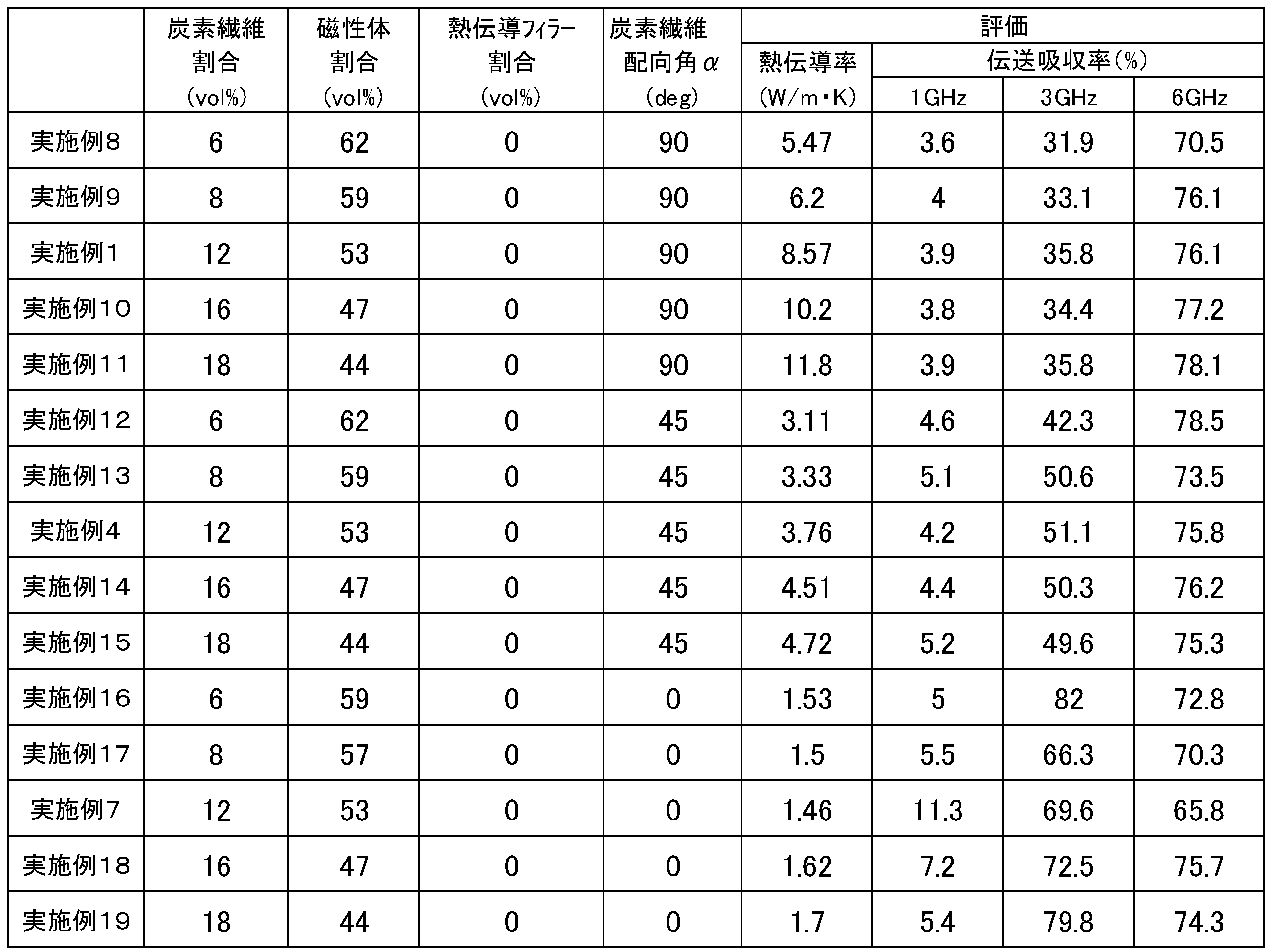
表1の結果から、実施例1、2では、熱伝導率が6W/(m・K)以上と高く、伝送吸収率も、特に3GHz帯で35%以上、6GHz帯では76%以上となり、特に高周波領域で優れた特性を示している。実施例3、4では、熱伝導率が3.8W/(m・K)以上と比較的高く、伝送吸収率も、3GHz帯で約40%以上、6GHz帯では75%以上となり、少し低い周波数領域の特性が向上している。実施例5~7では、熱伝導率が2.7~1.5W/(m・K)と少し低くなるものの、伝送吸収率が、1GHz帯でも5弱以上、3GHz帯より高周波領域では、70%弱以上と特に優れた特性を示すことがわかった。
このように、実施例1~7では、優れた熱伝導率及び伝送吸収率が得られ、更に炭素繊維の配向角により、熱伝導率と伝送吸収率の適切なバランス設定が可能となることがわかった。
一方、比較例を見ると、磁性体を含まず炭素繊維とシリカだけで構成した、比較例1及び2では、伝送吸収率が著しく小さく、比較例3では、熱伝導率及び伝送吸収率が共に小さくなっていることがわかった。磁性体のみで構成した比較例4では、熱伝導率が著しく小さくなっていることがわかった。また、炭素繊維の配向処理をしていない比較例5、6では、炭素繊維又は熱伝導フィラーの配向がないこと以外は同様の条件である実施例1及び比較例1と比べると、熱伝導性に劣ることがわかった。
このように、実施例1~7では、優れた熱伝導率及び伝送吸収率が得られ、更に炭素繊維の配向角により、熱伝導率と伝送吸収率の適切なバランス設定が可能となることがわかった。
一方、比較例を見ると、磁性体を含まず炭素繊維とシリカだけで構成した、比較例1及び2では、伝送吸収率が著しく小さく、比較例3では、熱伝導率及び伝送吸収率が共に小さくなっていることがわかった。磁性体のみで構成した比較例4では、熱伝導率が著しく小さくなっていることがわかった。また、炭素繊維の配向処理をしていない比較例5、6では、炭素繊維又は熱伝導フィラーの配向がないこと以外は同様の条件である実施例1及び比較例1と比べると、熱伝導性に劣ることがわかった。
また、表2では、炭素繊維配向角90°、45°、0°における炭素繊維と磁性体の含有割合を変えた場合の、熱伝導率及び伝送吸収率の特性値を示しているが、炭素繊維の配向角と共に、炭素繊維と磁性体の含有割合を調整することにより、多様な熱伝導率及び伝送吸収率の特性値設定ができることがわかった。
また、図4~6では、伝送吸収率の周波数特性を比較したが、炭素繊維のどの配向角αにおいても、炭素繊維で構成された比較例及び磁性体で構成された比較例に比べて、炭素繊維及び磁性体の両方を混在させた実施例では、相乗効果によってより優れた伝送吸収率を示すことがわかった。
本発明によれば、優れた熱伝導性及び電磁波吸収性を有する、電磁波吸収熱伝導シート及びその製造方法を提供することが可能となる。また、かかる電磁波吸収熱伝導シートを用い、放熱性及び電磁波抑制に優れた半導体装置を提供することが可能となる。
1 電磁波吸収熱伝導シート
2 ヒートスプレッダ
2a 主面
2b 側壁
2c 他の面
3 電子部品
3a 上面
5 ヒートシンク
6 配線基板
10 電磁波吸収熱伝導シート
11 高分子マトリックス成分
12 炭素繊維
13 磁性金属粉
100 測定系
110 ネットワークアナライザ
111 電磁波吸収熱伝導シートのサンプル
112 マイクロストリップライン
2 ヒートスプレッダ
2a 主面
2b 側壁
2c 他の面
3 電子部品
3a 上面
5 ヒートシンク
6 配線基板
10 電磁波吸収熱伝導シート
11 高分子マトリックス成分
12 炭素繊維
13 磁性金属粉
100 測定系
110 ネットワークアナライザ
111 電磁波吸収熱伝導シートのサンプル
112 マイクロストリップライン
Claims (14)
- 高分子マトリックス成分と、磁性金属粉と、一方向に配向している繊維状の熱伝導性充填剤とを含むことを特徴とする、電磁波吸収熱伝導シート。
- 前記繊維状の熱伝導性充填剤の配向方向が、シート面の延在方向に対して60°超え~90°の範囲であることを特徴とする、請求項1に記載の電磁波吸収熱伝導シート。
- 前記電磁波吸収熱伝導シートの、厚さ方向の熱伝導率が5W/(m・K)以上、3GHzでの伝送吸収率が30%以上、6GHzでの伝送吸収率が70%以上であることを特徴とする、請求項2に記載の電磁波吸収熱伝導シート。
- 前記繊維状の熱伝導性充填剤の配向方向が、シート面の延在方向に対して30°超え~60°の範囲であることを特徴とする、請求項1に記載の電磁波吸収熱伝導シート。
- 前記電磁波吸収熱伝導シートの、厚さ方向の熱伝導率が2.7W/(m・K)以上、3GHzでの伝送吸収率が39%以上、6GHzでの伝送吸収率が70%以上であることを特徴とする、請求項4に記載の電磁波吸収熱伝導シート。
- 前記繊維状の熱伝導性充填剤の配向方向が、シート面の延在方向に対して0°~30°の範囲であることを特徴とする、請求項1に記載の電磁波吸収熱伝導シート。
- 前記電磁波吸収熱伝導シートの、厚さ方向の熱伝導率が1.5W/(m・K)以上、3GHzでの伝送吸収率が68%以上、6GHzでの伝送吸収率が70%以上であることを特徴とする、請求項6に記載の電磁波吸収熱伝導シート。
- 前記繊維状の熱伝導性充填剤の含有量が4~40体積%、前記磁性金属粉の含有量が35~75体積%であることを特徴とする、請求項1~7のいずれか1項に記載の電磁波吸収熱伝導シート。
- 前記繊維状の熱伝導性充填剤の含有量が5~30体積%、前記磁性金属粉の含有量が40~65体積%であることを特徴とする、請求項8に記載の電磁波吸収熱伝導シート。
- 前記繊維状の熱伝導性充填剤が、炭素繊維であることを特徴とする、請求項1~9のいずれか1項に記載の電磁波吸収熱伝導シート。
- 前記電磁波吸収熱伝導シートが、無機物フィラーをさらに含むことを特徴とする、請求項1~10のいずれか1項に記載の電磁波吸収熱伝導シート。
- 高分子マトリックス成分と、繊維状の熱伝導性充填剤と、磁性金属粉とを含むシート用組成物を調製する工程と、
前記繊維状の熱伝導性充填剤を配向させる工程と、
前記繊維状の熱伝導性充填剤の配向を維持した状態で、前記高分子マトリックス成分を硬化させて、シート用成形体を作製する工程と、
前記配向した繊維状の熱伝導性充填剤の長軸方向に対して、0°~90°の角度となるように、前記シート用成形体を切断し、電磁波吸収熱伝導シートを作製する工程と、
を含むことを特徴とする、電磁波吸収熱伝導シートの製造方法。 - 前記繊維状の熱伝導性充填剤を配向させる工程が、中空状の型内に、前記シート用組成物を、高剪断力下で押し出すこと又は圧入することによって行われ、
前記シート用成形体を作製する工程が、前記高分子マトリックス成分を熱硬化させることによって行われることを特徴とする、請求項12に記載の電磁波吸収熱伝導シートの製造方法。 - 熱源と、放熱部材と、該熱源と該放熱部材との間に挟持された電磁波吸収熱伝導シートを備える半導体装置であって、
前記電磁波吸収熱伝導シートが、請求項1~11のいずれか1項に記載の電磁波吸収熱伝導シートであることを特徴とする、半導体装置。
Priority Applications (5)
| Application Number | Priority Date | Filing Date | Title |
|---|---|---|---|
| US16/085,263 US10892204B2 (en) | 2016-03-25 | 2017-03-24 | Electromagnetic wave absorbing heat conductive sheet, method for producing electromagnetic wave absorbing heat conductive sheet, and semiconductor device |
| KR1020187026385A KR102053004B1 (ko) | 2016-03-25 | 2017-03-24 | 전자파 흡수 열전도 시트, 전자파 흡수 열전도 시트의 제조 방법 및 반도체 장치 |
| KR1020197035407A KR102071443B1 (ko) | 2016-03-25 | 2017-03-24 | 전자파 흡수 열전도 시트, 전자파 흡수 열전도 시트의 제조 방법 및 반도체 장치 |
| CN201780017965.3A CN108886881B (zh) | 2016-03-25 | 2017-03-24 | 电磁波吸收导热片、电磁波吸收导热片的制造方法及半导体装置 |
| CN202010909764.8A CN112055513B (zh) | 2016-03-25 | 2017-03-24 | 电磁波吸收导热片 |
Applications Claiming Priority (2)
| Application Number | Priority Date | Filing Date | Title |
|---|---|---|---|
| JP2016062335A JP6366627B2 (ja) | 2016-03-25 | 2016-03-25 | 電磁波吸収熱伝導シート、電磁波吸収熱伝導シートの製造方法及び半導体装置 |
| JP2016-062335 | 2016-03-25 |
Publications (1)
| Publication Number | Publication Date |
|---|---|
| WO2017164406A1 true WO2017164406A1 (ja) | 2017-09-28 |
Family
ID=59899582
Family Applications (1)
| Application Number | Title | Priority Date | Filing Date |
|---|---|---|---|
| PCT/JP2017/012155 Ceased WO2017164406A1 (ja) | 2016-03-25 | 2017-03-24 | 電磁波吸収熱伝導シート、電磁波吸収熱伝導シートの製造方法及び半導体装置 |
Country Status (5)
| Country | Link |
|---|---|
| US (1) | US10892204B2 (ja) |
| JP (1) | JP6366627B2 (ja) |
| KR (2) | KR102071443B1 (ja) |
| CN (2) | CN112055513B (ja) |
| WO (1) | WO2017164406A1 (ja) |
Cited By (3)
| Publication number | Priority date | Publication date | Assignee | Title |
|---|---|---|---|---|
| EP3644699A1 (en) * | 2018-10-25 | 2020-04-29 | Seiko Epson Corporation | Printed circuit board, electronic device and heat conduction sheet |
| US20210029854A1 (en) * | 2018-03-30 | 2021-01-28 | Dupont Teijin Advanced Papers (Japan), Ltd. | Electromagnetic wave absorbing sheet and method for producing same |
| WO2021237140A1 (en) | 2020-05-22 | 2021-11-25 | Laird Technologies Inc. | Thermally-conductive electromagnetic interference (emi) absorbers including aluminum powder |
Families Citing this family (26)
| Publication number | Priority date | Publication date | Assignee | Title |
|---|---|---|---|---|
| US11229147B2 (en) | 2015-02-06 | 2022-01-18 | Laird Technologies, Inc. | Thermally-conductive electromagnetic interference (EMI) absorbers with silicon carbide |
| US10834854B2 (en) * | 2017-02-28 | 2020-11-10 | Northeastern University | Methods for the manufacture of thermal interfaces, thermal interfaces, and articles comprising the same |
| KR102488873B1 (ko) * | 2018-01-18 | 2023-01-17 | 삼성전자주식회사 | 전자파 차폐구조 |
| CN112352476A (zh) * | 2018-07-12 | 2021-02-09 | 迪睿合株式会社 | 拾取装置、安装装置、拾取方法、安装方法 |
| WO2020013333A1 (ja) * | 2018-07-12 | 2020-01-16 | デクセリアルズ株式会社 | ピックアップ装置、実装装置、ピックアップ方法、実装方法 |
| JP7196470B2 (ja) * | 2018-08-30 | 2022-12-27 | 日本電気株式会社 | 電子機器の放熱構造 |
| US10462944B1 (en) * | 2018-09-25 | 2019-10-29 | Getac Technology Corporation | Wave absorbing heat dissipation structure |
| CN110189883A (zh) * | 2019-06-05 | 2019-08-30 | 珠海天基探测技术有限公司 | 一种电流互感器柔性软磁铁芯 |
| JP6737979B1 (ja) * | 2019-06-10 | 2020-08-12 | 富士高分子工業株式会社 | 電磁波吸収性熱伝導性組成物及びそのシート |
| CN112218511A (zh) * | 2019-07-12 | 2021-01-12 | 南开大学 | 复合材料、其制备方法及用途 |
| CN110740629B (zh) * | 2019-10-16 | 2021-07-13 | 深圳市飞鸿达科技有限公司 | 一种定向导热吸波片及其制备方法 |
| US11482465B2 (en) * | 2019-10-18 | 2022-10-25 | Taiwan Semiconductor Manufacturing Company, Ltd. | Thermal interface materials, 3D semiconductor packages and methods of manufacture |
| KR102173914B1 (ko) * | 2020-03-31 | 2020-11-04 | 주식회사 케이넷츠 | 고방사 열전도성 방열판의 제조 방법 |
| CN113539989B (zh) * | 2020-04-13 | 2023-07-21 | 烽火通信科技股份有限公司 | 一种多芯片散热封装结构及封装方法 |
| KR102542423B1 (ko) * | 2020-09-23 | 2023-06-12 | 라이르드 테크놀로지스, 아이엔씨 | 열전도성 전자파 장해(emi) 흡수체 |
| SE545290C2 (en) * | 2020-10-09 | 2023-06-20 | Mxwaves Ab | Absorption sheet, system and method for performing radiation characterization |
| JP2021050350A (ja) * | 2020-12-07 | 2021-04-01 | デクセリアルズ株式会社 | 熱伝導性シート及びその製造方法、熱伝導性シートの実装方法 |
| JP2022124615A (ja) * | 2021-02-16 | 2022-08-26 | デクセリアルズ株式会社 | 熱伝導シート |
| CN113013118B (zh) | 2021-02-20 | 2024-03-08 | 英韧科技股份有限公司 | 应用磁性盖封装的封装级芯片、芯片模组及电子产品 |
| JP7701793B2 (ja) * | 2021-02-24 | 2025-07-02 | デクセリアルズ株式会社 | 熱伝導シート及び熱伝導シートの製造方法 |
| WO2022181171A1 (ja) * | 2021-02-24 | 2022-09-01 | デクセリアルズ株式会社 | 熱伝導シート及び熱伝導シートの製造方法 |
| CN117396542A (zh) * | 2021-05-26 | 2024-01-12 | 日产自动车株式会社 | 导热膜以及使用了该导热膜的散热结构体 |
| JP7669251B2 (ja) * | 2021-11-09 | 2025-04-28 | 株式会社東芝 | 電磁波減衰体及び電子装置 |
| WO2023190423A1 (ja) * | 2022-03-30 | 2023-10-05 | タツタ電線株式会社 | 導電性接着剤層及び放熱構造 |
| CN115373497B (zh) * | 2022-08-31 | 2026-04-17 | 联想(北京)有限公司 | 一种电子设备及导热吸波材料 |
| CN118201337B (zh) * | 2024-05-16 | 2024-08-16 | 浙江大华技术股份有限公司 | 吸波散热器及其制备方法、电子设备 |
Citations (2)
| Publication number | Priority date | Publication date | Assignee | Title |
|---|---|---|---|---|
| JP2011134755A (ja) * | 2009-12-22 | 2011-07-07 | Tdk Corp | 電磁ノイズ対策部材 |
| JP2012023335A (ja) * | 2010-06-17 | 2012-02-02 | Sony Chemical & Information Device Corp | 熱伝導性シート及びその製造方法 |
Family Cites Families (11)
| Publication number | Priority date | Publication date | Assignee | Title |
|---|---|---|---|---|
| JPS513780A (en) | 1974-06-28 | 1976-01-13 | Sharp Kk | Banpuojusuru handotaisochino seizohoho |
| JP2001068312A (ja) | 1999-08-26 | 2001-03-16 | Fuji Elelctrochem Co Ltd | 電波吸収熱伝導シート |
| US20060128895A1 (en) * | 2001-02-15 | 2006-06-15 | Thomas Aisenbrey | Electriplast thermoset wet mix material and method of manufacture |
| JP2004200534A (ja) * | 2002-12-20 | 2004-07-15 | Shin Etsu Chem Co Ltd | 電磁波吸収性熱伝導性シート |
| JP5103780B2 (ja) | 2006-04-18 | 2012-12-19 | 戸田工業株式会社 | 電磁波干渉抑制シート、高周波信号用フラットケーブル、フレキシブルプリント基板 |
| KR100849496B1 (ko) * | 2007-06-01 | 2008-07-31 | 한국전자통신연구원 | 목표 주파수 대역에서 방열 특성과 전자파 차폐 및 흡수특성을 지닌 복합 시트용 조성물 및 상기 조성물로 제조된단층형 복합 시트 |
| JP2010183033A (ja) * | 2009-02-09 | 2010-08-19 | Sony Corp | 電磁波抑制放熱用組成物及び電磁波抑制放熱用組成物の製造方法 |
| WO2011158942A1 (ja) | 2010-06-17 | 2011-12-22 | ソニーケミカル&インフォメーションデバイス株式会社 | 熱伝導性シート及びその製造方法 |
| JP2012044084A (ja) * | 2010-08-23 | 2012-03-01 | Sony Chemical & Information Device Corp | 電磁波吸収性熱伝導シート及び電磁波吸収性熱伝導シートの製造方法 |
| JP2013118313A (ja) * | 2011-12-05 | 2013-06-13 | Dexerials Corp | 電磁波吸収性熱伝導シート及び電磁波吸収性熱伝導シートの製造方法 |
| KR101625264B1 (ko) * | 2013-05-30 | 2016-05-27 | 제일모직주식회사 | 방열 접착 필름, 이를 포함하는 반도체 장치 및 상기 장치의 제조 방법 |
-
2016
- 2016-03-25 JP JP2016062335A patent/JP6366627B2/ja active Active
-
2017
- 2017-03-24 US US16/085,263 patent/US10892204B2/en active Active
- 2017-03-24 WO PCT/JP2017/012155 patent/WO2017164406A1/ja not_active Ceased
- 2017-03-24 KR KR1020197035407A patent/KR102071443B1/ko active Active
- 2017-03-24 CN CN202010909764.8A patent/CN112055513B/zh active Active
- 2017-03-24 KR KR1020187026385A patent/KR102053004B1/ko active Active
- 2017-03-24 CN CN201780017965.3A patent/CN108886881B/zh active Active
Patent Citations (2)
| Publication number | Priority date | Publication date | Assignee | Title |
|---|---|---|---|---|
| JP2011134755A (ja) * | 2009-12-22 | 2011-07-07 | Tdk Corp | 電磁ノイズ対策部材 |
| JP2012023335A (ja) * | 2010-06-17 | 2012-02-02 | Sony Chemical & Information Device Corp | 熱伝導性シート及びその製造方法 |
Cited By (7)
| Publication number | Priority date | Publication date | Assignee | Title |
|---|---|---|---|---|
| US20210029854A1 (en) * | 2018-03-30 | 2021-01-28 | Dupont Teijin Advanced Papers (Japan), Ltd. | Electromagnetic wave absorbing sheet and method for producing same |
| EP3644699A1 (en) * | 2018-10-25 | 2020-04-29 | Seiko Epson Corporation | Printed circuit board, electronic device and heat conduction sheet |
| JP2020068336A (ja) * | 2018-10-25 | 2020-04-30 | セイコーエプソン株式会社 | プリント回路板、電子機器、および熱伝導シート |
| JP7145413B2 (ja) | 2018-10-25 | 2022-10-03 | セイコーエプソン株式会社 | プリント回路板、電子機器、および熱伝導シート |
| WO2021237140A1 (en) | 2020-05-22 | 2021-11-25 | Laird Technologies Inc. | Thermally-conductive electromagnetic interference (emi) absorbers including aluminum powder |
| CN115669248A (zh) * | 2020-05-22 | 2023-01-31 | 莱尔德技术股份有限公司 | 包括铝粉的导热电磁干扰emi吸收体 |
| US12289876B2 (en) | 2020-05-22 | 2025-04-29 | Laird Technologies, Inc. | Thermally-conductive electromagnetic interference (EMI) absorbers including aluminum powder |
Also Published As
| Publication number | Publication date |
|---|---|
| KR102053004B1 (ko) | 2019-12-06 |
| US20190080978A1 (en) | 2019-03-14 |
| KR20190136115A (ko) | 2019-12-09 |
| CN108886881A (zh) | 2018-11-23 |
| JP2017175080A (ja) | 2017-09-28 |
| CN108886881B (zh) | 2020-09-29 |
| JP6366627B2 (ja) | 2018-08-01 |
| KR102071443B1 (ko) | 2020-01-30 |
| KR20180124867A (ko) | 2018-11-21 |
| CN112055513A (zh) | 2020-12-08 |
| CN112055513B (zh) | 2023-03-28 |
| US10892204B2 (en) | 2021-01-12 |
Similar Documents
| Publication | Publication Date | Title |
|---|---|---|
| JP6366627B2 (ja) | 電磁波吸収熱伝導シート、電磁波吸収熱伝導シートの製造方法及び半導体装置 | |
| JP6379320B1 (ja) | 電磁波吸収熱伝導シート、電磁波吸収熱伝導シートの製造方法及び半導体装置 | |
| WO2018079240A1 (ja) | 熱伝導シート、熱伝導シートの製造方法及び半導体装置 | |
| WO2018061712A1 (ja) | 電磁波吸収熱伝導シート、電磁波吸収熱伝導シートの製造方法及び半導体装置 | |
| JP6301978B2 (ja) | 熱伝導シート、熱伝導シートの製造方法、放熱部材及び半導体装置 | |
| WO2019193868A1 (ja) | 半導体装置 | |
| JP2018107272A (ja) | 半導体装置 | |
| WO2018147228A1 (ja) | 電磁波抑制熱伝導シート、電磁波抑制熱伝導シートの製造方法及び半導体装置 | |
| TWI714804B (zh) | 熱傳導片及半導體裝置 | |
| JP7598197B2 (ja) | 5g通信用アンテナアレイ、アンテナ構造、ノイズ抑制熱伝導シート及び熱伝導シート | |
| KR102445111B1 (ko) | 반도체 장치 및 반도체 장치의 제조 방법 | |
| WO2019244950A1 (ja) | 半導体装置及び半導体装置の製造方法 | |
| WO2020202939A1 (ja) | 5g通信用アンテナアレイ、アンテナ構造、ノイズ抑制熱伝導シート及び熱伝導シート | |
| US20240120254A1 (en) | Thermally-conductive sheet and electronic device | |
| JP2018022923A (ja) | 熱伝導シート、熱伝導シートの製造方法、放熱部材及び半導体装置 | |
| JP6379319B1 (ja) | 半導体装置 | |
| WO2022176823A1 (ja) | 熱伝導シート |
Legal Events
| Date | Code | Title | Description |
|---|---|---|---|
| DPE1 | Request for preliminary examination filed after expiration of 19th month from priority date (pct application filed from 20040101) | ||
| ENP | Entry into the national phase |
Ref document number: 20187026385 Country of ref document: KR Kind code of ref document: A |
|
| NENP | Non-entry into the national phase |
Ref country code: DE |
|
| 121 | Ep: the epo has been informed by wipo that ep was designated in this application |
Ref document number: 17770446 Country of ref document: EP Kind code of ref document: A1 |
|
| 122 | Ep: pct application non-entry in european phase |
Ref document number: 17770446 Country of ref document: EP Kind code of ref document: A1 |