WO2017164229A1 - 磁気トンネル接合素子の熱安定性指数の測定方法および測定システム、半導体集積回路、ならびに半導体集積回路の生産管理方法 - Google Patents
磁気トンネル接合素子の熱安定性指数の測定方法および測定システム、半導体集積回路、ならびに半導体集積回路の生産管理方法 Download PDFInfo
- Publication number
- WO2017164229A1 WO2017164229A1 PCT/JP2017/011408 JP2017011408W WO2017164229A1 WO 2017164229 A1 WO2017164229 A1 WO 2017164229A1 JP 2017011408 W JP2017011408 W JP 2017011408W WO 2017164229 A1 WO2017164229 A1 WO 2017164229A1
- Authority
- WO
- WIPO (PCT)
- Prior art keywords
- tunnel junction
- magnetic tunnel
- thermal stability
- stability index
- resistance state
- Prior art date
- Legal status (The legal status is an assumption and is not a legal conclusion. Google has not performed a legal analysis and makes no representation as to the accuracy of the status listed.)
- Ceased
Links
Images



Classifications
-
- H—ELECTRICITY
- H10—SEMICONDUCTOR DEVICES; ELECTRIC SOLID-STATE DEVICES NOT OTHERWISE PROVIDED FOR
- H10P—GENERIC PROCESSES OR APPARATUS FOR THE MANUFACTURE OR TREATMENT OF DEVICES COVERED BY CLASS H10
- H10P74/00—Testing or measuring during manufacture or treatment of wafers, substrates or devices
- H10P74/27—Structural arrangements therefor
- H10P74/273—Interconnections for measuring or testing, e.g. probe pads
-
- H—ELECTRICITY
- H10—SEMICONDUCTOR DEVICES; ELECTRIC SOLID-STATE DEVICES NOT OTHERWISE PROVIDED FOR
- H10N—ELECTRIC SOLID-STATE DEVICES NOT OTHERWISE PROVIDED FOR
- H10N50/00—Galvanomagnetic devices
- H10N50/01—Manufacture or treatment
-
- G—PHYSICS
- G01—MEASURING; TESTING
- G01R—MEASURING ELECTRIC VARIABLES; MEASURING MAGNETIC VARIABLES
- G01R31/00—Arrangements for testing electric properties; Arrangements for locating electric faults; Arrangements for electrical testing characterised by what is being tested not provided for elsewhere
- G01R31/28—Testing of electronic circuits, e.g. by signal tracer
- G01R31/2851—Testing of integrated circuits [IC]
- G01R31/2855—Environmental, reliability or burn-in testing
- G01R31/2872—Environmental, reliability or burn-in testing related to electrical or environmental aspects, e.g. temperature, humidity, vibration, nuclear radiation
- G01R31/2874—Environmental, reliability or burn-in testing related to electrical or environmental aspects, e.g. temperature, humidity, vibration, nuclear radiation related to temperature
-
- G—PHYSICS
- G01—MEASURING; TESTING
- G01R—MEASURING ELECTRIC VARIABLES; MEASURING MAGNETIC VARIABLES
- G01R27/00—Arrangements for measuring resistance, reactance, impedance, or electric characteristics derived therefrom
- G01R27/02—Measuring real or complex resistance, reactance, impedance, or other two-pole characteristics derived therefrom, e.g. time constant
-
- G—PHYSICS
- G01—MEASURING; TESTING
- G01R—MEASURING ELECTRIC VARIABLES; MEASURING MAGNETIC VARIABLES
- G01R31/00—Arrangements for testing electric properties; Arrangements for locating electric faults; Arrangements for electrical testing characterised by what is being tested not provided for elsewhere
- G01R31/28—Testing of electronic circuits, e.g. by signal tracer
- G01R31/2851—Testing of integrated circuits [IC]
- G01R31/2894—Aspects of quality control [QC]
-
- G—PHYSICS
- G11—INFORMATION STORAGE
- G11C—STATIC STORES
- G11C11/00—Digital stores characterised by the use of particular electric or magnetic storage elements; Storage elements therefor
- G11C11/02—Digital stores characterised by the use of particular electric or magnetic storage elements; Storage elements therefor using magnetic elements
- G11C11/16—Digital stores characterised by the use of particular electric or magnetic storage elements; Storage elements therefor using magnetic elements using elements in which the storage effect is based on magnetic spin effect
-
- H—ELECTRICITY
- H10—SEMICONDUCTOR DEVICES; ELECTRIC SOLID-STATE DEVICES NOT OTHERWISE PROVIDED FOR
- H10B—ELECTRONIC MEMORY DEVICES
- H10B61/00—Magnetic memory devices, e.g. magnetoresistive RAM [MRAM] devices
-
- H—ELECTRICITY
- H10—SEMICONDUCTOR DEVICES; ELECTRIC SOLID-STATE DEVICES NOT OTHERWISE PROVIDED FOR
- H10B—ELECTRONIC MEMORY DEVICES
- H10B61/00—Magnetic memory devices, e.g. magnetoresistive RAM [MRAM] devices
- H10B61/20—Magnetic memory devices, e.g. magnetoresistive RAM [MRAM] devices comprising components having three or more electrodes, e.g. transistors
- H10B61/22—Magnetic memory devices, e.g. magnetoresistive RAM [MRAM] devices comprising components having three or more electrodes, e.g. transistors of the field-effect transistor [FET] type
-
- H—ELECTRICITY
- H10—SEMICONDUCTOR DEVICES; ELECTRIC SOLID-STATE DEVICES NOT OTHERWISE PROVIDED FOR
- H10D—INORGANIC ELECTRIC SEMICONDUCTOR DEVICES
- H10D84/00—Integrated devices formed in or on semiconductor substrates that comprise only semiconducting layers, e.g. on Si wafers or on GaAs-on-Si wafers
- H10D84/80—Integrated devices formed in or on semiconductor substrates that comprise only semiconducting layers, e.g. on Si wafers or on GaAs-on-Si wafers characterised by the integration of at least one component covered by groups H10D12/00 or H10D30/00, e.g. integration of IGFETs
-
- H—ELECTRICITY
- H10—SEMICONDUCTOR DEVICES; ELECTRIC SOLID-STATE DEVICES NOT OTHERWISE PROVIDED FOR
- H10N—ELECTRIC SOLID-STATE DEVICES NOT OTHERWISE PROVIDED FOR
- H10N50/00—Galvanomagnetic devices
- H10N50/10—Magnetoresistive devices
-
- H—ELECTRICITY
- H10—SEMICONDUCTOR DEVICES; ELECTRIC SOLID-STATE DEVICES NOT OTHERWISE PROVIDED FOR
- H10N—ELECTRIC SOLID-STATE DEVICES NOT OTHERWISE PROVIDED FOR
- H10N50/00—Galvanomagnetic devices
- H10N50/80—Constructional details
-
- H—ELECTRICITY
- H10—SEMICONDUCTOR DEVICES; ELECTRIC SOLID-STATE DEVICES NOT OTHERWISE PROVIDED FOR
- H10P—GENERIC PROCESSES OR APPARATUS FOR THE MANUFACTURE OR TREATMENT OF DEVICES COVERED BY CLASS H10
- H10P72/00—Handling or holding of wafers, substrates or devices during manufacture or treatment thereof
- H10P72/06—Apparatus for monitoring, sorting, marking, testing or measuring
- H10P72/0602—Temperature monitoring
-
- H—ELECTRICITY
- H10—SEMICONDUCTOR DEVICES; ELECTRIC SOLID-STATE DEVICES NOT OTHERWISE PROVIDED FOR
- H10P—GENERIC PROCESSES OR APPARATUS FOR THE MANUFACTURE OR TREATMENT OF DEVICES COVERED BY CLASS H10
- H10P74/00—Testing or measuring during manufacture or treatment of wafers, substrates or devices
- H10P74/20—Testing or measuring during manufacture or treatment of wafers, substrates or devices characterised by the properties tested or measured, e.g. structural or electrical properties
- H10P74/207—Electrical properties, e.g. testing or measuring of resistance, deep levels or capacitance-voltage characteristics
-
- G—PHYSICS
- G01—MEASURING; TESTING
- G01R—MEASURING ELECTRIC VARIABLES; MEASURING MAGNETIC VARIABLES
- G01R27/00—Arrangements for measuring resistance, reactance, impedance, or electric characteristics derived therefrom
-
- H—ELECTRICITY
- H10—SEMICONDUCTOR DEVICES; ELECTRIC SOLID-STATE DEVICES NOT OTHERWISE PROVIDED FOR
- H10P—GENERIC PROCESSES OR APPARATUS FOR THE MANUFACTURE OR TREATMENT OF DEVICES COVERED BY CLASS H10
- H10P74/00—Testing or measuring during manufacture or treatment of wafers, substrates or devices
- H10P74/23—Testing or measuring during manufacture or treatment of wafers, substrates or devices characterised by multiple measurements, corrections, marking or sorting processes
Definitions
- the present invention relates to a method and system for measuring a thermal stability index of a magnetic tunnel junction element, a semiconductor integrated circuit, and a production management method for a semiconductor integrated circuit.
- a non-volatile memory such as an MRAM having a magnetoresistive effect element has a thermal stability index as an indication of the thermal stability of bit information.
- E b energy barrier required for the magnetization reversal
- k B Boltzmann constant
- T absolute temperature
- E b K eff V
- Is K eff: anisotropy energy density of the recording layer
- V volume of the recording layer).
- the energy of the recording layer of the magnetoresistive element is expressed by K eff V ⁇ sin 2 ⁇ (where ⁇ is an angle formed by the magnetization direction of the recording layer and the magnetization direction of the reference layer), and sin 2
- the time t when P is 50% is the retention time of the recording layer.
- the magnetic field pulse method measures the magnetization reversal probability when applying a magnetic field pulse with a specific pulse width while changing the magnetic field size of the magnetic field pulse, and based on the relationship between the magnetic field size and the reversal probability, and requests the sexual index delta 0 (for example, see non-Patent Document 2).
- the current pulse method measures the magnetization reversal probability when a current pulse of a specific pulse width is given while changing the current magnitude of the current pulse, and based on the relationship between the current magnitude and the reversal probability, and requests the thermal stability index delta 0 (for example, see non-Patent Document 3).
- Non-Patent Document 6 the method for measuring the thermal stability index described in Non-Patent Document 6 is to measure the thermal stability index of the chip and not to measure the thermal stability index in units of elements such as MTJ. there were.
- an MRAM chip having a capacity of several Mb or more is necessary.
- it takes time to obtain data When used for quality control (QC check) at the production site, there is a problem that a lot of time is wasted.
- QC check quality control
- the thermal stability index is increased, there is a problem that the measurement time is increased.
- the present invention has been made paying attention to such problems, and can measure the thermal stability index for each element in a relatively short time, and can quickly perform material development and quality control at the production site. It is an object of the present invention to provide a method and system for measuring the thermal stability index of a magnetic tunnel junction device capable of performing semiconductor manufacturing, a semiconductor integrated circuit, and a production management method for a semiconductor integrated circuit.
- a method for measuring a thermal stability index of a magnetic tunnel junction device includes: a magnetic tunnel junction device that is maintained at a predetermined temperature; First measurement for determining a time constant for maintaining a low resistance state and a time constant for maintaining a high resistance state from a measurement step for measuring a change in resistance value of the junction element and a change in the resistance value measured in the measurement step And a second calculation step for obtaining a thermal stability index of the magnetic tunnel junction element based on the predetermined current and each time constant obtained in the first calculation step.
- the method and system for measuring the thermal stability index of a magnetic tunnel junction device does not require the generation of a magnetic field at the time of measurement, and performs measurement on an element basis, not on an entire chip having many elements. Therefore, the thermal stability index can be measured in a relatively short time. Further, since the manner of the magnetic field pulse method or a current pulse method, the value of energy barrier E b does not change during the measurement, it is possible to obtain an accurate thermal stability index.
- the method and system for measuring the thermal stability index of a magnetic tunnel junction element according to the present invention may measure only a single element or a plurality of single elements. You may measure.
- the method and system for measuring the thermal stability index of a magnetic tunnel junction element according to the present invention can measure the thermal stability index in units of magnetic tunnel junction elements, the management information based on the measurement results is used for the manufacturing process of the chip. It is not necessary to feed back to the first stage, and it is sufficient to feed back to the manufacturing stage of the magnetic tunnel junction element. This saves time from the start of chip manufacture to the previous stage of manufacturing the magnetic tunnel junction device, compared to the case of feedback to the first stage of the chip manufacturing process. Quality control can be performed quickly.
- the measurement step includes sequentially supplying a plurality of currents having different magnitudes as the predetermined current, and sequentially changing the resistance value for each current.
- a time constant ⁇ P for holding the low resistance state and a time constant ⁇ AP for holding the high resistance state are obtained for each current, and the second calculation is performed.
- the first calculation step may be a frequency of a time during which a low resistance state is maintained from a change in the resistance value measured in the measurement step.
- the distribution N P (t) and the frequency distribution N AP (t) of the time for maintaining the high resistance state are obtained, and N P (t) texp ( ⁇ t / ⁇ P ) and N AP (t) ⁇ exp ( ⁇ It is preferable to obtain the time constant ⁇ P for maintaining the low resistance state and the time constant ⁇ AP for maintaining the high resistance state using the relationship of t / ⁇ AP ).
- the analysis means determines the frequency distribution N P of the time during which a low resistance state is maintained from the change in the resistance value measured by the measurement means. t) and the frequency distribution N AP (t) of the time for maintaining the high resistance state are obtained, and N P (t) texp ( ⁇ t / ⁇ P ) and N AP (t) ⁇ exp ( ⁇ t / ⁇ AP , respectively) It is preferable that the time constant ⁇ P for maintaining the low resistance state and the time constant ⁇ AP for maintaining the high resistance state are obtained using the relationship of In this case, a more accurate thermal stability index can be obtained.
- the second calculation step holds the predetermined current I and the low resistance state obtained in the first calculation step.
- ⁇ P / ( ⁇ P + ⁇ AP ) 1 / [1 + exp ⁇ 0 ⁇ (2 ⁇ I / I c0 ) ⁇ ] (4) It is preferable to obtain the thermal stability index ⁇ 0 and the threshold current value I c0 using the following formula.
- the analysis means includes the predetermined current I and a time constant ⁇ P for maintaining the low resistance state obtained in the first calculation step, and It is preferable that the thermal stability index ⁇ 0 and the threshold current value I c0 are obtained using the equation (4) based on the time constant ⁇ AP for maintaining the high resistance state. In this case, a more accurate thermal stability index can be obtained.
- the measurement step is electrically connected only to the magnetic tunnel junction element so that a current flows only through the magnetic tunnel junction element.
- the change in the resistance value may be measured while flowing the predetermined current from the inspection terminal to the magnetic tunnel junction element.
- the system for measuring the thermal stability index of a magnetic tunnel junction element according to the present invention has an inspection terminal electrically connected only to the magnetic tunnel junction element so that a current flows only through the magnetic tunnel junction element.
- the measuring means may be configured to measure a change in the resistance value while flowing the predetermined current from the inspection terminal to the magnetic tunnel junction element. In this case, an accurate thermal stability index of a single magnetic tunnel junction element can be obtained using the inspection terminal.
- the semiconductor integrated circuit according to the present invention is a semiconductor integrated circuit having a plurality of magnetic tunnel junction elements, and is electrically connected only to the magnetic tunnel junction element so that a current flows only through the single magnetic tunnel junction element. It has a terminal for inspection.
- the inspection terminals are composed of a pair of terminals, and these terminals only need to be electrically connected to only a single magnetic tunnel junction element.
- the inspection terminal is preferably configured by an upper wiring, a lower wiring, and a connection region (VIA) of the magnetic tunnel junction element.
- the inspection terminal is provided in each of one magnetic tunnel junction element or a plurality of magnetic tunnel junction elements.
- one or a plurality of magnetic tunnel junction elements provided with inspection terminals can be measured and inspected, and a thermal stability index can be obtained.
- a production management method for a semiconductor integrated circuit according to the present invention is a production management method for a semiconductor integrated circuit having a plurality of magnetic tunnel junction elements, wherein the plurality of magnetic tunnel junctions are manufactured after the plurality of magnetic tunnel junction elements are manufactured.
- a thermal stability index is obtained by a method for measuring a thermal stability index of the magnetic tunnel junction element according to the present invention, and the plurality of magnetic tunnels are based on the obtained thermal stability index. It is characterized by managing a process of manufacturing a junction element.
- the production management method for a semiconductor integrated circuit according to the present invention measures the thermal stability index for each magnetic tunnel junction element by the method for measuring the thermal stability index of the magnetic tunnel junction element according to the present invention.
- the management information based on this need not be fed back to the initial stage of the chip manufacturing process, but may be fed back to the manufacturing stage of the magnetic tunnel junction element. This saves time from the start of chip manufacture to the previous stage of manufacturing the magnetic tunnel junction device, compared to the case of feeding back to the first stage of the chip manufacturing process, and enables rapid production management. Can do.
- the semiconductor integrated circuit is preferably the semiconductor integrated circuit according to the present invention.
- the thermal stability index of each element can be measured in a relatively short time, and the thermal stability index of the magnetic tunnel junction element can be quickly developed for material development and quality control at the production site. Measurement method and measurement system, semiconductor integrated circuit, and semiconductor integrated circuit production management method can be provided.
- FIG. 1 It is a perspective view which shows the MTJ array structure of the semiconductor integrated circuit of embodiment of this invention.
- A Example of observation waveform of resistance value of MTJ for evaluation using oscilloscope,
- b Time for maintaining low resistance state or high resistance by the method for measuring the thermal stability index of the magnetic tunnel junction device according to the embodiment of the present invention
- a graph showing an example of a frequency distribution of time for holding a state and a curve obtained by fitting;
- FIG. 1 to 6 show a method and system for measuring a thermal stability index of a magnetic tunnel junction device according to an embodiment of the present invention, a semiconductor integrated circuit, and a production management method for a semiconductor integrated circuit.
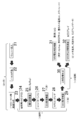
- the upper wiring 15 is formed on the MTJ 11 (step 30). Normally, this step 30 ends within two weeks.
- an electrical characteristic inspection for the single MTJ 11 (step 31) and a characteristic inspection for the MTJ array are performed (step 32).
- the electrical property inspection for the MTJ 11 for example, the resistance value, thermal stability, write current, error rate, and the like are inspected.
- the characteristic inspection for the MTJ array for example, inspection of a bit defect rate, resistance distribution, and the like is performed.
- the CMOS 13 and the intermediate wiring 14 connected to the CMOS 13 shown in FIG. 1 are not electrically connected, and are electrically connected only to the evaluation MTJ 11a.
- an inspection terminal block 17 including the intermediate wiring 14, the connection area (VIA) 16, and the upper wiring 15 is formed.
- the inspection terminal block 17 is composed of a pair of terminals, one terminal is composed of the upper wiring 15 formed on the upper part of the single evaluation MTJ 11a, and the other terminal is It consists of an intermediate wiring (BASE) 14 connected to the lower part of the MTJ 11a for evaluation, a connection region 16 formed thereon, and an upper wiring 15.
- the inspection terminal block 17 is configured to allow a current to flow only through a single evaluation MTJ 11 a that is electrically connected, and can be used for the electrical characteristic inspection in step 31.
- one to several test terminal blocks 17 may be arranged as single TEG (Test Element Group) areas at corners in the memory chip. As shown in FIG. 4B, one to several pieces may be arranged for each subarray in the memory chip. These one to several test element blocks 17 are connected to the upper wiring 15 which is completely independent of a pad group for externally connecting to a bit line or word line of a memory array, which will be described later.
- Pad 17a For example, a probe such as a prober is brought into contact with the pad 17a to electrically connect to various electrical measurement devices, and the characteristics of the evaluation MTJ 11a are electrically measured.
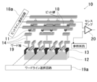
- the bit line selection circuit 18a and the word line selection circuit 19a apply voltages to predetermined bit lines 18 and word lines 19, respectively, based on the write bit number. Is applied. Further, when reading from an arbitrary MTJ 11, a predetermined bit line 18 and word line 19 are selected by the bit line selection circuit 18a and the word line selection circuit 19a based on the read bit number, respectively, and the sense amplifier 20 To connect to.
- the characteristic inspection for the MTJ array in step 32 of FIG. 2 can be performed using the circuit shown in FIG.
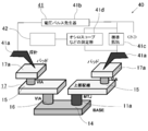
- the measurement system 40 of the thermal stability index of the magnetic tunnel junction element according to the embodiment of the present invention includes a heat retaining means (not shown), a measuring means 41, and an analyzing means 42. .
- the heat retaining means is composed of a temperature-controllable prober, and can hold the wafer 12 including the evaluation MTJ 11a so as to be maintained at a predetermined temperature.
- the measuring means 41 includes a pair of probes 41a of a prober as a heat retaining means, for example, a voltage pulse generator 41b, a standard resistor 41c, and a voltage measuring instrument 41d.
- the voltage pulse generator 41b is connected to each probe 41a, and a voltage pulse can be applied between each probe 41a.
- the standard resistor 41c is connected in series between one probe 41a and the voltage pulse generator 41b.
- the measuring means 41 makes the evaluation by bringing each probe 41a into contact with each inspection terminal block 17 of the evaluation MTJ 11a, generating a predetermined voltage pulse by the voltage pulse generator 41b, and applying it to both ends of the evaluation MTJ 11a.
- a predetermined current is passed through the MTJ 11a.
- the voltage generated at both ends of the standard resistor 41c generated by the current is measured by monitoring the voltage measuring device 41d for a predetermined time, thereby measuring the change in resistance value of the evaluation MTJ 11a. .
- the analyzing means 42 is composed of a computer and is connected to a voltage measuring device 41d so that the measured value can be inputted.
- the analyzing means 42 obtains a time constant for holding the low resistance state and a time constant for holding the high resistance state from the change in the resistance value measured by the voltage measuring device 41d. Further, the thermal stability index of the evaluation MTJ 11a is obtained based on the obtained time constants and the current passed through the evaluation MTJ 11a.
- the method for measuring the thermal stability index of the magnetic tunnel junction element according to the embodiment of the present invention can be preferably implemented by the measurement system 40 for the thermal stability index of the magnetic tunnel junction element shown in FIG. That is, in the method for measuring the thermal stability index of the magnetic tunnel junction element according to the embodiment of the present invention, first, the evaluation MTJ 11a is held at a predetermined temperature by the heat retention means, and then the measurement MT 41 is changed to the evaluation MTJ 11a. While flowing a predetermined current, a change in the resistance value of the evaluation MTJ 11a is measured for a predetermined time.
- FIG. 6A shows a specific measurement example with the voltage measuring instrument 41d composed of an oscilloscope at this time. The measurement temperature is 240 ° C. The measurement time in FIG. 6A is 500 ⁇ m. As shown to Fig.6 (a), it can confirm that the low resistance state and the high resistance state exist in the change of the measured resistance value.
- the frequency distribution N P (t) for holding the low resistance state and the frequency distribution N AP (t) for holding the high resistance state are obtained from the change in the measured resistance value by the analyzing means 42. From the attenuation state, by using the relation of N P (t) ⁇ exp ( ⁇ t / ⁇ P ) and N AP (t) ⁇ exp ( ⁇ t / ⁇ AP ), respectively, by fitting such as the least square method
- the time constant ⁇ P for maintaining the low resistance state and the time constant ⁇ AP for maintaining the high resistance state are obtained.
- FIG. 6B shows an example of the frequency distribution N P, AP (t) of the time for holding the low resistance state or the time for holding the high resistance state obtained by actual measurement at this time, and the curve obtained by fitting. Shown in
- the analysis means 42 keeps the low resistance state corresponding to each current.
- a constant ⁇ P and a time constant ⁇ AP for maintaining a high resistance state are obtained.
- FIG. 6C shows an example of the relationship between each current obtained by actual measurement at this time and the left side ⁇ P / ( ⁇ P + ⁇ AP ) of the equation (4) and a curve obtained by fitting.
- the thermal stability index ⁇ 0 24.69
- the threshold current value I c0 175.44 ⁇ A.
- the thermal stability index at any operating temperature including room temperature can be easily obtained from measurements performed at high temperatures.
- the time constant ⁇ P and the time constant ⁇ AP for maintaining the high resistance state are obtained.
- the current is a DC current sufficient to monitor the resistance state, and the magnetic field pulse (strength H) is changed.
- a time constant ⁇ P for maintaining a low resistance state and a time constant ⁇ AP for maintaining a high resistance state are obtained for each magnetic field.
- the thermal stability index ⁇ 0 and the threshold magnetic field H C0 can also be obtained.
- the measurement method and the measurement system 40 of the thermal stability index of the magnetic tunnel junction element according to the embodiment of the present invention do not need to generate a magnetic field at the time of measurement, and not the entire chip having many elements.
- order to measure only the single evaluation MTJ11a it is possible to measure the thermal stability index delta 0 evaluation MTJ11a unitary in a relatively short time.
- the value of energy barrier E b at the time of measurement does not change, it is possible to obtain an accurate thermal stability index delta 0 evaluation MTJ11a unitary.
- the semiconductor integrated circuit production management method of the embodiment of the present invention it is necessary to feed back management information based on the measurement result of the evaluation MTJ 11a to the first stage (step 21) of the chip manufacturing process. There is no. For this reason, it is possible to save the period from the start of chip manufacture to the previous stage of manufacturing the MTJ 11 (step 21 to step 23), compared to the case of feeding back to the first stage of the chip manufacturing process. For example, in the manufacturing process shown in FIG. 2, two months from step 21 to step 23 can be saved, and material development, quality control at the production site, and production management can be performed quickly.
Landscapes
- Engineering & Computer Science (AREA)
- Physics & Mathematics (AREA)
- General Physics & Mathematics (AREA)
- Computer Hardware Design (AREA)
- Environmental & Geological Engineering (AREA)
- Microelectronics & Electronic Packaging (AREA)
- General Engineering & Computer Science (AREA)
- Manufacturing & Machinery (AREA)
- Toxicology (AREA)
- Health & Medical Sciences (AREA)
- Mram Or Spin Memory Techniques (AREA)
- Hall/Mr Elements (AREA)
- Testing Or Measuring Of Semiconductors Or The Like (AREA)
Abstract
Description
Δ0=Eb/kBT (1)
で表される(Eb:磁化反転に要するエネルギー障壁、kB:ボルツマン定数、T:絶対温度)。ここで、
Eb=KeffV (2)
である(Keff:記録層の磁気異方性エネルギー密度、V:記録層の体積)。
P=1-exp{(-t/10-9)×exp(-Δ0)} (3)
で与えられる(例えば、非特許文献1参照)。なお、Pが50%のときの時間tが、記録層の保持時間である。
τP/(τP+τAP)=1/[1+exp{-Δ0・(2×I/Ic0)}]
(4)
の式を用いて、熱安定性指数Δ0およびしきい電流値Ic0を求めることが好ましい。本発明に係る磁気トンネル接合素子の熱安定性指数の測定システムで、前記解析手段は、前記所定の電流Iと、前記第1計算工程で求めた前記低抵抗状態を保持する時定数τPおよび前記高抵抗状態を保持する時定数τAPとに基づいて、(4)式を用いて、熱安定性指数Δ0およびしきい電流値Ic0を求めるよう構成されていることが好ましい。この場合、さらに正確な熱安定性指数を求めることができる。
図1乃至図6は、本発明の実施の形態の磁気トンネル接合素子の熱安定性指数の測定方法および測定システム、半導体集積回路、ならびに半導体集積回路の生産管理方法を示している。
図1に示すように、本発明の実施の形態の半導体集積回路10は、多数のMTJ(磁気トンネル接合素子)11を有するMRAM(磁気抵抗メモリ)から成り、図2に示す製造工程に従って製造される。
こうして、図2に示す製造方法に従って、MRAMのメモリチップから成る半導体集積回路10を製造することができる。
次に、図2のステップ31における単体の評価用MTJ11aに対する電気特性検査のうち、熱安定性指数の測定を行うための、本発明の実施の形態の磁気トンネル接合素子の熱安定性指数の測定方法および測定システムについて説明する。
図3に示すように、本発明の実施の形態の磁気トンネル接合素子の熱安定性指数の測定システム40は、保温手段(図示せず)と測定手段41と解析手段42とを有している。
τP/(τP+τAP)=1/[1+exp{-Δ0・(4×H/HC0)}]
(5)
次に、本発明の実施の形態の半導体集積回路の生産管理方法について説明する。
図2のステップ31において、メモリチップ上の1または複数の評価用MTJ11aに対して、本発明の実施の形態の磁気トンネル接合素子の熱安定性指数の測定方法および測定システム40により熱安定性指数を求めたならば、その熱安定性指数に基づいて、ステップ24~ステップ29までのMTJ製造工程の管理を行う。例えば、所望の熱安定性指数が得られないときには、ステップ24までフィードバックして、MTJ11の製造条件の変更等を行えばよい。
11 MTJ
12 ウェハー
13 CMOS
14 中間配線
15 上部配線
16 接続領域
17 検査用端子ブロック
17a パッド
18 ビット線
18a ビットライン選択回路
19 ワード線
19a ワードライン選択回路
20 センスアンプ
40 磁気トンネル接合素子の熱安定性指数の測定システム
41 測定手段
41a 探針
41b 電圧パルス発生器
41c 標準抵抗
41d 電圧測定器
42 解析手段
Claims (15)
- 所定の温度に保持した磁気トンネル接合素子に所定の電流を流しながら、所定時間、前記磁気トンネル接合素子の抵抗値の変化を測定する測定工程と、
前記測定工程で測定された前記抵抗値の変化から、低抵抗状態を保持する時定数および高抵抗状態を保持する時定数を求める第1計算工程と、
前記所定の電流と、前記第1計算工程で求めた各時定数とに基づいて、前記磁気トンネル接合素子の熱安定性指数を求める第2計算工程とを、
有することを特徴とする磁気トンネル接合素子の熱安定性指数の測定方法。 - 前記測定工程は、前記所定の電流として、異なる大きさの複数の電流を順番に流しながら、各電流についてそれぞれ前記抵抗値の変化を測定し、
前記第1計算工程は、各電流に対応して、それぞれ前記低抵抗状態を保持する時定数τPおよび前記高抵抗状態を保持する時定数τAPを求め、
前記第2計算工程は、各電流の大きさと、各電流に対応したτPおよびτAPとに基づいて、前記熱安定性指数を求めることを
特徴とする請求項1記載の磁気トンネル接合素子の熱安定性指数の測定方法。 - 前記第1計算工程は、前記測定工程で測定された前記抵抗値の変化から、低抵抗状態を保持する時間の頻度分布NP(t)および高抵抗状態を保持する時間の頻度分布NAP(t)を求め、それぞれNP(t)∝exp(-t/τP)およびNAP(t)∝exp(-t/τAP) の関係を用いて、前記低抵抗状態を保持する時定数τPおよび前記高抵抗状態を保持する時定数τAPを求めることを特徴とする請求項1または2記載の磁気トンネル接合素子の熱安定性指数の測定方法。
- 前記第2計算工程は、前記所定の電流Iと、前記第1計算工程で求めた前記低抵抗状態を保持する時定数τPおよび前記高抵抗状態を保持する時定数τAPとに基づいて、
τP/(τP+τAP)=1/[1+exp{-Δ0・(2×I/Ic0)}]
の式を用いて、熱安定性指数Δ0およびしきい電流値Ic0を求めることを特徴とする請求項1乃至3のいずれか1項に記載の磁気トンネル接合素子の熱安定性指数の測定方法。 - 前記測定工程は、前記磁気トンネル接合素子のみに電流を流すよう、その磁気トンネル接合素子のみに電気的に接続された検査用端子から前記磁気トンネル接合素子に前記所定の電流を流しながら、前記抵抗値の変化を測定することを特徴とする請求項1乃至4のいずれか1項に記載の磁気トンネル接合素子の熱安定性指数の測定方法。
- 磁気トンネル接合素子を所定の温度に保持する保温手段と、
前記磁気トンネル接合素子に所定の電流を流しながら、所定時間、前記磁気トンネル接合素子の抵抗値の変化を測定する測定手段と、
前記測定手段で測定された前記抵抗値の変化から、低抵抗状態を保持する時定数および高抵抗状態を保持する時定数を求め、その各時定数と前記所定の電流とに基づいて、前記磁気トンネル接合素子の熱安定性指数を求める解析手段とを、
有することを特徴とする磁気トンネル接合素子の熱安定性指数の測定システム。 - 前記測定手段は、前記所定の電流として、異なる大きさの複数の電流を順番に流しながら、各電流についてそれぞれ前記抵抗値の変化を測定するよう構成され、
前記解析手段は、各電流に対応して、それぞれ前記低抵抗状態を保持する時定数τPおよび前記高抵抗状態を保持する時定数τAPを求め、各電流の大きさと、各電流に対応したτPおよびτAPとに基づいて、前記熱安定性指数を求めるよう構成されていることを
特徴とする請求項6記載の磁気トンネル接合素子の熱安定性指数の測定システム。 - 前記解析手段は、前記測定手段で測定された前記抵抗値の変化から、低抵抗状態を保持する時間の頻度分布NP(t)および高抵抗状態を保持する時間の頻度分布NAP(t)を求め、それぞれNP(t)∝exp(-t/τP)およびNAP(t)∝exp(-t/τAP) の関係を用いて、前記低抵抗状態を保持する時定数τPおよび前記高抵抗状態を保持する時定数τAPを求めるよう構成されていることを特徴とする請求項6または7記載の磁気トンネル接合素子の熱安定性指数の測定システム。
- 前記解析手段は、前記所定の電流Iと、前記第1計算工程で求めた前記低抵抗状態を保持する時定数τPおよび前記高抵抗状態を保持する時定数τAPとに基づいて、
τP/(τP+τAP)=1/[1+exp{-Δ0・(2×I/Ic0)}]
の式を用いて、熱安定性指数Δ0およびしきい電流値Ic0を求めるよう構成されていることを特徴とする請求項6乃至8のいずれか1項に記載の磁気トンネル接合素子の熱安定性指数の測定システム。 - 前記磁気トンネル接合素子のみに電流を流すよう、その磁気トンネル接合素子のみに電気的に接続された検査用端子を有し、
前記測定手段は、前記検査用端子から前記磁気トンネル接合素子に前記所定の電流を流しながら、前記抵抗値の変化を測定するよう構成されていることを
特徴とする請求項6乃至9のいずれか1項に記載の磁気トンネル接合素子の熱安定性指数の測定システム。 - 複数の磁気トンネル接合素子を有する半導体集積回路であって、
単体の磁気トンネル接合素子のみに電流を流すよう、その磁気トンネル接合素子のみに電気的に接続された検査用端子を有することを
特徴とする半導体集積回路。 - 前記検査用端子は、1つの磁気トンネル接合素子または複数の磁気トンネル接合素子のそれぞれに設けられていることを特徴とする請求項11記載の半導体集積回路。
- 前記検査用端子は、請求項1乃至4のいずれか1項に記載の磁気トンネル接合素子の熱安定性指数の測定方法の前記測定工程で、前記所定の電流を流すとともに前記抵抗値の変化を測定するために使用されることを特徴とする請求項11または12記載の半導体集積回路。
- 複数の磁気トンネル接合素子を有する半導体集積回路の生産管理方法であって、
前記複数の磁気トンネル接合素子を製造した後、前記複数の磁気トンネル接合素子のうちの1または複数について、請求項1乃至5のいずれか1項に記載の磁気トンネル接合素子の熱安定性指数の測定方法により熱安定性指数を求め、求められた前記熱安定性指数に基づいて、前記複数の磁気トンネル接合素子を製造する工程を管理することを
特徴とする半導体集積回路の生産管理方法。 - 前記半導体集積回路は、請求項11乃至13のいずれか1項に記載の半導体集積回路であることを特徴とする請求項14記載の半導体集積回路の生産管理方法。
Priority Applications (3)
| Application Number | Priority Date | Filing Date | Title |
|---|---|---|---|
| JP2018507365A JP6841517B2 (ja) | 2016-03-24 | 2017-03-22 | 磁気トンネル接合素子の熱安定性指数の測定方法および測定システム、ならびに半導体集積回路の生産管理方法 |
| KR1020187026530A KR102356201B1 (ko) | 2016-03-24 | 2017-03-22 | 자기 터널 접합 소자의 열안정성 지수의 측정 방법 및 측정 시스템, 반도체 집적회로, 및 반도체 집적회로의 생산관리 방법 |
| US16/087,781 US11054463B2 (en) | 2016-03-24 | 2017-03-22 | Method and system for measuring thermal stability factor of magnetic tunnel junction device, semiconductor integrated circuit, and production management method for semiconductor integrated circuit |
Applications Claiming Priority (2)
| Application Number | Priority Date | Filing Date | Title |
|---|---|---|---|
| JP2016-059344 | 2016-03-24 | ||
| JP2016059344 | 2016-03-24 |
Publications (1)
| Publication Number | Publication Date |
|---|---|
| WO2017164229A1 true WO2017164229A1 (ja) | 2017-09-28 |
Family
ID=59899433
Family Applications (1)
| Application Number | Title | Priority Date | Filing Date |
|---|---|---|---|
| PCT/JP2017/011408 Ceased WO2017164229A1 (ja) | 2016-03-24 | 2017-03-22 | 磁気トンネル接合素子の熱安定性指数の測定方法および測定システム、半導体集積回路、ならびに半導体集積回路の生産管理方法 |
Country Status (4)
| Country | Link |
|---|---|
| US (1) | US11054463B2 (ja) |
| JP (1) | JP6841517B2 (ja) |
| KR (1) | KR102356201B1 (ja) |
| WO (1) | WO2017164229A1 (ja) |
Cited By (3)
| Publication number | Priority date | Publication date | Assignee | Title |
|---|---|---|---|---|
| WO2019194450A1 (ko) * | 2018-04-04 | 2019-10-10 | 한양대학교 산학협력단 | Stt-mram에서 결함 mtj 셀 검증 방법 및 시스템 |
| WO2024101254A1 (ja) * | 2022-11-09 | 2024-05-16 | ソニーセミコンダクタソリューションズ株式会社 | 磁気検出装置及びデコーディングシステム |
| CN121432120A (zh) * | 2025-12-31 | 2026-01-30 | 苏州凌存科技有限公司 | 磁隧道结器件组热稳定性的测试方法及测试系统 |
Families Citing this family (5)
| Publication number | Priority date | Publication date | Assignee | Title |
|---|---|---|---|---|
| CN112444765B (zh) * | 2019-08-30 | 2024-08-02 | 中电海康集团有限公司 | 翻转电压的测试方法 |
| CN112712846B (zh) * | 2019-10-25 | 2023-05-23 | 浙江驰拓科技有限公司 | 磁存储器测试方法及系统 |
| CN115911001A (zh) * | 2021-08-27 | 2023-04-04 | 浙江驰拓科技有限公司 | 阻性存储器的测试结构及方法 |
| EP4276481A1 (en) * | 2022-05-13 | 2023-11-15 | Hamilton Sundstrand Corporation | Transient voltage suppressor condition monitoring |
| CN118566624B (zh) * | 2024-07-26 | 2024-10-15 | 北京易动宇航科技有限公司 | 一种盘式双保持式电磁铁性能检测方法及设备 |
Citations (2)
| Publication number | Priority date | Publication date | Assignee | Title |
|---|---|---|---|---|
| JP2006202999A (ja) * | 2005-01-20 | 2006-08-03 | Tdk Corp | 薄膜素子の製造方法及びウエハ |
| JP2009026944A (ja) * | 2007-07-19 | 2009-02-05 | Sony Corp | 記憶素子及びメモリ |
Family Cites Families (2)
| Publication number | Priority date | Publication date | Assignee | Title |
|---|---|---|---|---|
| JP4380693B2 (ja) * | 2006-12-12 | 2009-12-09 | ソニー株式会社 | 記憶素子、メモリ |
| JP5062597B2 (ja) * | 2008-08-29 | 2012-10-31 | 独立行政法人産業技術総合研究所 | トンネル磁気抵抗素子 |
-
2017
- 2017-03-22 JP JP2018507365A patent/JP6841517B2/ja active Active
- 2017-03-22 WO PCT/JP2017/011408 patent/WO2017164229A1/ja not_active Ceased
- 2017-03-22 US US16/087,781 patent/US11054463B2/en active Active
- 2017-03-22 KR KR1020187026530A patent/KR102356201B1/ko active Active
Patent Citations (2)
| Publication number | Priority date | Publication date | Assignee | Title |
|---|---|---|---|---|
| JP2006202999A (ja) * | 2005-01-20 | 2006-08-03 | Tdk Corp | 薄膜素子の製造方法及びウエハ |
| JP2009026944A (ja) * | 2007-07-19 | 2009-02-05 | Sony Corp | 記憶素子及びメモリ |
Cited By (4)
| Publication number | Priority date | Publication date | Assignee | Title |
|---|---|---|---|---|
| WO2019194450A1 (ko) * | 2018-04-04 | 2019-10-10 | 한양대학교 산학협력단 | Stt-mram에서 결함 mtj 셀 검증 방법 및 시스템 |
| US11988702B2 (en) | 2018-04-04 | 2024-05-21 | Samsung Electronics Co., Ltd. | Method and system for inspection of defective MTJ cell in STT-MRAM |
| WO2024101254A1 (ja) * | 2022-11-09 | 2024-05-16 | ソニーセミコンダクタソリューションズ株式会社 | 磁気検出装置及びデコーディングシステム |
| CN121432120A (zh) * | 2025-12-31 | 2026-01-30 | 苏州凌存科技有限公司 | 磁隧道结器件组热稳定性的测试方法及测试系统 |
Also Published As
| Publication number | Publication date |
|---|---|
| KR102356201B1 (ko) | 2022-01-26 |
| US11054463B2 (en) | 2021-07-06 |
| JP6841517B2 (ja) | 2021-03-10 |
| KR20180125472A (ko) | 2018-11-23 |
| JPWO2017164229A1 (ja) | 2019-02-07 |
| US20190219633A1 (en) | 2019-07-18 |
Similar Documents
| Publication | Publication Date | Title |
|---|---|---|
| JP6841517B2 (ja) | 磁気トンネル接合素子の熱安定性指数の測定方法および測定システム、ならびに半導体集積回路の生産管理方法 | |
| Min et al. | A study of write margin of spin torque transfer magnetic random access memory technology | |
| TW201101302A (en) | In-situ resistance measurement for magnetic random access memory (MRAM) | |
| TWI379096B (en) | Digital magnetic current sensor and logic | |
| CN108333539B (zh) | 测量图案化装置级的交换劲度的方法 | |
| CN108109668B (zh) | 一种磁存储器的测试方法、装置、存储介质及电子装置 | |
| JP2004519809A (ja) | Mramセル用の基準 | |
| JP6887686B2 (ja) | 磁気トンネル接合素子を備える磁気メモリの製造方法 | |
| US20140252356A1 (en) | Devices and methods for measurement of magnetic characteristics of mram wafers using magnetoresistive test strips | |
| JP2023522718A (ja) | 試験サンプルの温度変調特性の測定 | |
| TWI829657B (zh) | 半導體裝置測試系統 | |
| CN1622221B (zh) | 分析磁性随机存取存储器的设备与方法 | |
| US8942032B2 (en) | Method for magnetic screening of arrays of magnetic memories | |
| US10971245B1 (en) | Measurement of MTJ in a compact memory array | |
| US7495456B2 (en) | System and method of determining pulse properties of semiconductor device | |
| JP2008539534A (ja) | Mramトグル・ビット特徴付けのための3連パルス方法 | |
| Van Beek et al. | Four point probe ramped voltage stress as an efficient method to understand breakdown of STT-MRAM MgO tunnel junctions | |
| Hosotani et al. | Effect of self-heating on time-dependent dielectric breakdown in ultrathin MgO magnetic tunnel junctions for spin torque transfer switching magnetic random access memory | |
| CN111223518A (zh) | 用于阻性存储单元的测试结构及耐久性测试方法 | |
| US9349427B2 (en) | Method for screening arrays of magnetic memories | |
| CN116018046B (zh) | 一种磁存储阵列的测试结构及测试方法 | |
| CN115683380A (zh) | 一种利用磁隧道结rkky耦合的温度依赖性测量温度的方法 | |
| Yatsyshyn et al. | Metrological Array of Cyber-Physical Systems. Part 12. Study of Quantum Unit of Temperature | |
| Hindenberg et al. | Offset Field Extraction With Multi-Bit Magnetic Tunnel Junction Structures | |
| CN111508549A (zh) | 一种sot-mram的测试结构及其测试方法 |
Legal Events
| Date | Code | Title | Description |
|---|---|---|---|
| ENP | Entry into the national phase |
Ref document number: 20187026530 Country of ref document: KR Kind code of ref document: A |
|
| WWE | Wipo information: entry into national phase |
Ref document number: 2018507365 Country of ref document: JP |
|
| NENP | Non-entry into the national phase |
Ref country code: DE |
|
| 121 | Ep: the epo has been informed by wipo that ep was designated in this application |
Ref document number: 17770269 Country of ref document: EP Kind code of ref document: A1 |
|
| 122 | Ep: pct application non-entry in european phase |
Ref document number: 17770269 Country of ref document: EP Kind code of ref document: A1 |