WO2017164228A1 - 送信装置、アンテナ駆動装置、チューニング方法、およびチューニング方法を実現するプログラム - Google Patents
送信装置、アンテナ駆動装置、チューニング方法、およびチューニング方法を実現するプログラム Download PDFInfo
- Publication number
- WO2017164228A1 WO2017164228A1 PCT/JP2017/011406 JP2017011406W WO2017164228A1 WO 2017164228 A1 WO2017164228 A1 WO 2017164228A1 JP 2017011406 W JP2017011406 W JP 2017011406W WO 2017164228 A1 WO2017164228 A1 WO 2017164228A1
- Authority
- WO
- WIPO (PCT)
- Prior art keywords
- unit
- antenna
- drive
- signal
- current
- Prior art date
- Legal status (The legal status is an assumption and is not a legal conclusion. Google has not performed a legal analysis and makes no representation as to the accuracy of the status listed.)
- Ceased
Links
Images






Classifications
-
- H—ELECTRICITY
- H04—ELECTRIC COMMUNICATION TECHNIQUE
- H04B—TRANSMISSION
- H04B5/00—Near-field transmission systems, e.g. inductive or capacitive transmission systems
- H04B5/40—Near-field transmission systems, e.g. inductive or capacitive transmission systems characterised by components specially adapted for near-field transmission
- H04B5/48—Transceivers
-
- H—ELECTRICITY
- H02—GENERATION; CONVERSION OR DISTRIBUTION OF ELECTRIC POWER
- H02J—ELECTRIC POWER NETWORKS; CIRCUIT ARRANGEMENTS OR SYSTEMS FOR SUPPLYING OR DISTRIBUTING ELECTRIC POWER; SYSTEMS FOR STORING ELECTRIC ENERGY
- H02J50/00—Circuit arrangements or systems for wireless supply or distribution of electric power
- H02J50/10—Circuit arrangements or systems for wireless supply or distribution of electric power using inductive coupling
- H02J50/12—Circuit arrangements or systems for wireless supply or distribution of electric power using inductive coupling of the resonant type
-
- H—ELECTRICITY
- H02—GENERATION; CONVERSION OR DISTRIBUTION OF ELECTRIC POWER
- H02J—ELECTRIC POWER NETWORKS; CIRCUIT ARRANGEMENTS OR SYSTEMS FOR SUPPLYING OR DISTRIBUTING ELECTRIC POWER; SYSTEMS FOR STORING ELECTRIC ENERGY
- H02J50/00—Circuit arrangements or systems for wireless supply or distribution of electric power
- H02J50/20—Circuit arrangements or systems for wireless supply or distribution of electric power using microwaves or radio frequency waves
-
- H—ELECTRICITY
- H04—ELECTRIC COMMUNICATION TECHNIQUE
- H04B—TRANSMISSION
- H04B1/00—Details of transmission systems, not covered by a single one of groups H04B3/00 - H04B13/00; Details of transmission systems not characterised by the medium used for transmission
- H04B1/02—Transmitters
- H04B1/04—Circuits
-
- H—ELECTRICITY
- H04—ELECTRIC COMMUNICATION TECHNIQUE
- H04B—TRANSMISSION
- H04B1/00—Details of transmission systems, not covered by a single one of groups H04B3/00 - H04B13/00; Details of transmission systems not characterised by the medium used for transmission
- H04B1/02—Transmitters
- H04B1/04—Circuits
- H04B1/0458—Arrangements for matching and coupling between power amplifier and antenna or between amplifying stages
-
- H—ELECTRICITY
- H04—ELECTRIC COMMUNICATION TECHNIQUE
- H04B—TRANSMISSION
- H04B1/00—Details of transmission systems, not covered by a single one of groups H04B3/00 - H04B13/00; Details of transmission systems not characterised by the medium used for transmission
- H04B1/06—Receivers
- H04B1/16—Circuits
- H04B1/18—Input circuits, e.g. for coupling to an antenna or a transmission line
-
- H—ELECTRICITY
- H04—ELECTRIC COMMUNICATION TECHNIQUE
- H04B—TRANSMISSION
- H04B5/00—Near-field transmission systems, e.g. inductive or capacitive transmission systems
- H04B5/70—Near-field transmission systems, e.g. inductive or capacitive transmission systems specially adapted for specific purposes
- H04B5/79—Near-field transmission systems, e.g. inductive or capacitive transmission systems specially adapted for specific purposes for data transfer in combination with power transfer
-
- G—PHYSICS
- G06—COMPUTING OR CALCULATING; COUNTING
- G06K—GRAPHICAL DATA READING; PRESENTATION OF DATA; RECORD CARRIERS; HANDLING RECORD CARRIERS
- G06K7/00—Methods or arrangements for sensing record carriers, e.g. for reading patterns
- G06K7/10—Methods or arrangements for sensing record carriers, e.g. for reading patterns by electromagnetic radiation, e.g. optical sensing; by corpuscular radiation
- G06K7/10009—Methods or arrangements for sensing record carriers, e.g. for reading patterns by electromagnetic radiation, e.g. optical sensing; by corpuscular radiation sensing by radiation using wavelengths larger than 0.1 mm, e.g. radio-waves or microwaves
- G06K7/10237—Methods or arrangements for sensing record carriers, e.g. for reading patterns by electromagnetic radiation, e.g. optical sensing; by corpuscular radiation sensing by radiation using wavelengths larger than 0.1 mm, e.g. radio-waves or microwaves the reader and the record carrier being capable of selectively switching between reader and record carrier appearance, e.g. in near field communication [NFC] devices where the NFC device may function as an RFID reader or as an RFID tag
Definitions
- the present invention relates to a technology such as a transmission device that performs non-contact communication or non-contact power feeding by electromagnetic coupling.
- NFC Near Field Communication
- R / W a transmission antenna of a reader / writer (hereinafter referred to as R / W) device dedicated to the system
- R / W a transmission antenna of a reader / writer
- the frequency of the signal source in the R / W device, the resonance frequency of the transmission antenna of the R / W device, and the reception in the non-contact IC card It is important that the resonance frequency of the antenna (resonant circuit) matches each other.
- the resonance frequency of the reception antenna of the non-contact IC card or the transmission antenna of the R / W device varies depending on various factors such as the environment in which the R / W device is used. In this case, it becomes difficult to stably transmit and receive information between the non-contact IC card and the R / W device.
- a booster may be provided for amplifying communication power.
- Patent Document 2 describes the necessity of using a booster.
- the communication distance between the non-contact type RFID R / W and the RFID tag is several centimeters.
- a variety of uses are conceivable in the RFID system in which various uses are considered, and it is desirable that the communication distance can be further extended depending on the application field.
- it has been proposed to arrange a booster antenna between the RFID tag and the RFID reader / writer (described in paragraph [0005] of the specification of Patent Document 2).
- Patent Document 3 discloses that a booster is provided to secure a communication distance even with a small antenna. Moreover, in this patent document 3, the detection circuit connected with the NFC controller produces
- booster antenna coil It is difficult to mount a booster antenna coil in a small transmitter such as a memory card. In addition, it is required to be controlled to an appropriate resonance frequency in various environments regardless of the presence or absence of a booster.
- An object of the present invention is to provide a technique such as a transmission apparatus that can appropriately control the resonance frequency of an antenna regardless of the presence or absence of a booster and thereby obtain stable communication characteristics.
- a transmission apparatus includes an antenna resonance unit, a drive unit, a detection unit, and a control unit.
- the antenna resonance unit includes an antenna coil and an impedance matching unit.
- the drive unit generates a transmission signal to the antenna resonance unit.
- the detection unit detects a driving current or driving power for operating the driving unit.
- the control unit is capable of generating a control signal for controlling the impedance matching unit, and using the optimal control value that minimizes the drive current or the drive power detected by the detection unit among the control signals, The resonance frequency of the antenna resonance unit is controlled.
- the resonance frequency is controlled so that the drive current for operating the drive unit or the drive power based on the drive current is minimized. It is possible to appropriately control the resonance frequency of the antenna in accordance with the change in the environment used, and to obtain stable communication characteristics.
- the control unit may be configured to detect the optimum control value by outputting the control signal within a predetermined search range.
- the detection unit may be configured to output an average value or an effective value of the drive current.
- the transmission device has an optimum time difference corresponding to a controlled amount in the impedance matching unit when the drive current or the drive power is minimized, and is an optimum of the transmission signal and the antenna current flowing through the antenna coil
- the transmission device may further include a measurement unit that measures a time difference between the transmission signal and an antenna current flowing through the antenna coil.
- the control unit obtains a time difference measured by the measurement unit by outputting the control signal within a predetermined search range, and based on a comparison result between the measured time difference and the optimum time difference, You may be comprised so that an optimal control value may be detected. Thereby, the transmission apparatus can use the optimal control value corresponding to the fluctuation
- the measurement unit includes a phase comparator that compares the phase of the transmission signal output from the drive unit and input to the antenna resonance unit with the phase of the antenna current.
- the drive unit receives a signal from the oscillation unit and the oscillation unit, and generates a first signal and a pair of differential signals each having a phase opposite to the phase of the first signal as the transmission signal. And an amplifier.
- the phase comparator may be configured to compare the phase of the first signal among the signals generated by the pair of differential amplifiers with the phase of the antenna current by the first signal.
- the driving unit receives an external driving unit that amplifies the antenna current, an oscillating unit, and a signal from the oscillating unit, and the transmission signal has a phase opposite to that of the first signal and the first signal.
- You may have a pair of differential amplifier which each produces
- the phase comparator may be configured to compare the phase of the first signal and the phase of the antenna current by the second signal among signals generated by the pair of differential amplifiers.
- the drive unit may include an external drive unit that amplifies the antenna current.
- a transmission device includes the antenna resonance unit described above, the drive unit described above, a measurement unit, and a control unit.
- the measurement unit measures a time difference between the transmission signal and an antenna current flowing through the antenna coil.
- the control unit can generate a control signal for controlling the impedance matching unit, and controls the resonance frequency of the antenna resonance unit using an optimum control value among the control signals.
- the optimum control value is a value corresponding to the optimum time difference when the drive current or drive power for operating the drive unit is minimized among the time difference measured by the measurement unit.
- the resonance frequency is controlled using the optimal time difference so that the drive current for driving the drive unit or the drive power based on the drive current is minimized. Regardless of this, it is possible to appropriately control the resonance frequency of the antenna and to obtain stable communication characteristics.
- An antenna drive device is an antenna drive device that drives an antenna resonance unit including an antenna coil and an impedance matching unit, and includes a generation unit, an acquisition unit, and a control unit.
- the generation unit generates a transmission signal to the antenna resonance unit.
- the acquisition unit acquires a value of the drive current detected by a detection unit that detects a drive current or drive power for operating the drive unit.
- the control unit is capable of generating a control signal for controlling the impedance matching unit, and using the optimal control value that minimizes the drive current or the drive power detected by the detection unit among the control signals, The resonance frequency of the antenna resonance unit is controlled.
- An antenna drive device is an antenna drive device that drives an antenna resonance unit including an antenna coil and an impedance matching unit, and includes the above-described generation unit, acquisition unit, and control unit. It has.
- the acquisition unit acquires the time difference measured by a measurement unit that measures a time difference between the transmission signal and an antenna current flowing through the antenna coil.
- the control unit can generate a control signal for controlling the impedance matching unit, and controls the resonance frequency of the antenna resonance unit using an optimum control value among the control signals.
- the optimum control value is a value corresponding to the optimum time difference when the drive current or drive power for operating the drive unit is minimized among the time difference measured by the measurement unit.
- a tuning method is a tuning method of a resonance frequency of the antenna resonance unit by a transmission device including the antenna resonance unit described above and the drive unit described above.
- a control signal for controlling the impedance matching unit is output.
- an optimal control value that minimizes the drive current or the drive power is detected from the control signal. Is done.
- a tuning method is a tuning method of a resonance frequency of the antenna resonance unit by a transmission device including the antenna resonance unit described above and the drive unit described above.
- a control signal for controlling the impedance matching unit is output.
- a time difference between the transmission signal and the antenna current flowing through the antenna coil is measured according to the output of the control signal.
- An optimal time difference corresponding to a controlled amount in the impedance matching unit when the driving current or driving power for operating the driving unit is minimized, and the transmission signal and the antenna coil
- a program for a transmission apparatus that executes the above tuning method can also be provided.
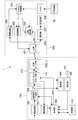
- FIG. 1 is a block diagram showing a configuration of a contactless communication system according to an embodiment of the present invention.
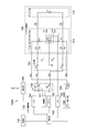
- FIG. 2 shows a circuit configuration of a transmission apparatus having no booster as the transmission apparatus shown in FIG.
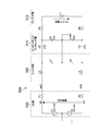
- FIG. 3 shows a circuit configuration of a transmission apparatus having a booster as the transmission apparatus shown in FIG.
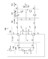
- FIG. 4 shows a basic circuit configuration of a transmission apparatus according to a reference example that does not have a booster.
- FIG. 5 shows a basic circuit configuration of a transmission device having a booster according to a reference example.
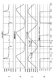
- 6A to 6C are graphs showing calculation results of signals of respective parts under resonance conditions in the transmission device according to the reference example shown in FIG. 7A to 7C are graphs showing signals of respective parts under resonance conditions in the transmission apparatus according to the reference example shown in FIG.
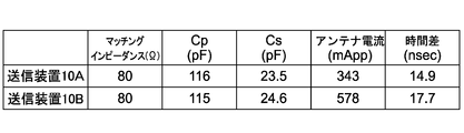
- FIG. 8 is a table summarizing resonance conditions for both a booster not having and a transmitter having it.
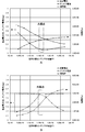
- FIG. 9A is a graph showing the relationship between the capacity Cp, the driving power, the antenna current, and the time difference for a transmission apparatus that does not have a booster.
- FIG. 9B is a graph showing the relationship between the capacity Cp, the driving power, the antenna current, and the time difference for the transmission device having a booster.
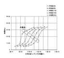
- FIG. 10 is a graph showing the relationship between the capacitance Cp, the antenna current, and the driving power for various values of matching impedance in a transmission device having a booster.
- FIG. 11 is a graph showing the relationship between the capacitance Cp and the time difference for various values of matching impedance in a transmission device having a booster.
- FIG. 9A is a graph showing the relationship between the capacity Cp, the driving power, the antenna current, and the time difference for a transmission apparatus that does not have a booster.
- FIG. 9B is a graph showing the relationship
- FIG. 12 is a graph showing the relationship between matching impedance, antenna current, time difference, and drive power in a transmission device having a booster.
- FIG. 13 is a flowchart showing a tuning method based on the minimum driving power method.
- FIG. 14 is a flowchart showing a tuning method based on the optimum time difference method.
- FIG. 15 is a block diagram illustrating a configuration of the non-contact power feeding system.
- FIG. 16 shows a circuit configuration of a transmission apparatus (power supply apparatus) having an external drive circuit in the non-contact power supply system.
- FIG. 17 shows the configuration of the external drive circuit.
- FIG. 1 is a block diagram showing a configuration of a contactless communication system according to an embodiment of the present invention.
- wiring related to input / output of information between circuit blocks is indicated by solid arrows, and wiring related to power supply is indicated by broken arrows.
- a contactless communication system 1 includes NFC (Near Field), which is a short-range wireless communication technology including NFC-A, NFC-B, NFC-F, and the like based on the international standard ISO / IEC18092. Communication).
- NFC Near Field
- the non-contact communication system 1 includes a transmission device 100 and a reception device 200.
- the non-contact communication system 1 transmits and receives information between the transmission device 100 and the reception device 200 by non-contact communication.
- Examples of the non-contact communication system 1 include a communication system that combines a non-contact IC card standard represented by Felica (registered trademark) and the NFC standard.
- the transmission device 100 will be described.
- the transmission device 100 is a device having a reader / writer (R / W) function for reading and writing data in a contactless manner with respect to the reception device 200.
- the transmission device 100 includes an antenna resonance unit 110, an antenna drive unit 130 (drive unit, antenna drive device) (see FIG. 2), a detection unit 106, and a storage unit 145.
- the antenna resonance unit 110 includes a primary antenna unit 112 and an impedance matching unit 114, and configures a resonance circuit including an antenna coil L1 and a resonance capacitor (variable capacitor) as will be described later. .
- the antenna resonating unit 110 transmits and receives signals to and from the secondary antenna unit 201 of the receiving device 200 by electromagnetic coupling.
- the primary side antenna unit 112 has a function of transmitting a transmission signal of a desired frequency by a resonance circuit and receiving a response signal from the receiving device 200.
- the impedance matching unit 114 has a function as a matching circuit that performs impedance matching between the transmission signal generation unit (generation unit) 101 of the antenna driving unit 130 and the primary side antenna unit 112.
- the control unit of the antenna driving unit 130 controls the impedance matching unit 114 as described later, whereby the impedance between the transmission signal generating unit 101 and the primary antenna unit 112 is controlled. Achieves optimization of matching and resonance frequency.
- the antenna driving unit 130 mainly includes a transmission signal generation unit 101, a modulation circuit 102, a demodulation circuit 103, and a control unit 140.
- the transmission signal generation unit 101 modulates a carrier signal having a desired frequency (for example, 13.56 MHz) with the transmission data input from the modulation circuit 102, and the modulated carrier signal is transmitted to the primary antenna via the impedance matching unit 114. A function of outputting to the unit 112.
- a desired frequency for example, 13.56 MHz
- the modulation circuit 102 has a function of encoding the transmission data input from the control unit 140 and outputting the encoded transmission data to the transmission signal generation unit 101.
- the demodulation circuit 103 has a function of acquiring the response signal received by the primary antenna unit 112 via the impedance matching unit 114 and demodulating the response signal.
- the demodulation circuit 103 has a function of outputting the demodulated response data to the control unit 140.
- the control unit 140 has a function of generating various control command signals in accordance with an external command or a built-in program, outputting the command signals to the modulation circuit 102, and controlling the operation of the circuit.
- the control unit 140 has a function of generating transmission data corresponding to the command signal and supplying the transmission data to the modulation circuit 102. Further, the control unit 140 has a function of performing predetermined processing based on the response data demodulated by the demodulation circuit 103.
- the control unit 140 has a function of controlling the R / W function and the card function of the transmission device 100.
- the R / W function is a function in which the transmission device 100 communicates (data read / write) with the reception device 200 that is a secondary device (partner device).
- the card function is a function of the receiving device 200 that is the secondary device illustrated in FIG. 1 and means that the transmitting device 100 has the function.
- control unit 140 generates a control signal (for example, control voltage) for controlling the impedance matching unit 114 and outputs the control signal to the impedance matching unit 114.
- a control signal for example, control voltage
- the impedance matching unit 114 includes a variable capacitor (variable capacitor), and the capacitance (controlled amount) of the variable capacitor is controlled by a control signal. Thereby, the resonance frequency of the antenna resonance unit 110 is controlled.
- the control unit 140 may be functionally or physically separated into a control unit that controls the entire system of the transmission device 100 and a transmission / reception control unit that controls transmission / reception of signals.
- the transmission / reception control unit is configured to mainly control the impedance matching unit 114 described above.
- the control unit 140 is mainly configured by, for example, a CPU (Central Processing Unit) and / or a PLD (Programmable Logic Device).
- a CPU Central Processing Unit
- PLD Programmable Logic Device
- the detecting unit 106 has a function of detecting a current supplied from the power source 107 connected to the antenna driving unit 130. This current is a drive current for operating the antenna drive unit 130 (and / or a booster described later).
- the receiving device 200 will be described.
- the receiving device 200 is configured by a mobile device that operates as a non-contact IC card is illustrated.
- the receiving device 200 has a function of controlling its own resonance frequency will be described.
- the receiving device 200 includes a secondary antenna unit 201 having a function as a receiving antenna, a rectifying unit 204, a reception control unit 202, a demodulation circuit 205, a system control unit 203, a modulation circuit 206, a constant voltage, Unit 207 and battery 208.
- the secondary antenna unit 201 has a resonance circuit composed of a resonance coil (not shown) and a plurality of resonance capacitors, for example.
- This resonance capacitor includes a variable capacitor whose capacitance is changed by applying a control voltage.
- the secondary side antenna unit 201 communicates with the primary side antenna unit 112 of the transmission device 100 by electromagnetic coupling, receives a magnetic field generated by the primary side antenna unit 112, and receives a transmission signal from the transmission device 100. It has a function. At this time, the capacitance of the variable capacitor is controlled so that the resonance frequency of the secondary antenna unit 201 becomes a desired frequency.
- the rectifying unit 204 is composed of, for example, a half-wave rectifier circuit including a rectifying diode and a rectifying capacitor. It has a function of outputting to the voltage unit 207.
- the constant voltage unit 207 performs voltage fluctuation (data component) suppression processing and stabilization processing on the electric signal (DC power) input from the rectification unit 204, and sends the processed DC power to the reception control unit 202. It has a function to supply. Note that the DC power output via the rectifying unit 204 and the constant voltage unit 207 is used as a power source for operating the IC in the receiving device 200.
- the reception control unit 202 has a function of controlling the resonance characteristics of the secondary side antenna unit 201 to optimize the resonance frequency during reception. Specifically, a control voltage is applied to a variable capacitor included in the secondary side antenna unit 201 to control its capacitance, thereby controlling the resonance frequency of the secondary side antenna unit 201.
- the demodulation circuit 205 has a function of demodulating the reception signal received by the secondary antenna unit 201 and outputting the demodulated signal to the system control unit 203.
- the system control unit 203 has a function of determining the contents based on the signal demodulated by the demodulation circuit 205, performing necessary processing, and controlling the modulation circuit 206 and the reception control unit 202.
- the modulation circuit 206 has a function of modulating the received carrier according to the result (contents of the demodulated signal) determined by the system control unit 203 to generate a response signal.
- the modulation circuit 206 has a function of outputting the generated response signal to the secondary antenna unit 201.
- the response signal output from the modulation circuit 206 is transmitted from the secondary antenna unit 201 to the primary antenna unit 112 by non-contact communication.
- the battery 208 has a function of supplying power to the system control unit 203.
- the battery 208 is charged by connecting its charging terminal to the external power source 50.
- the receiving device 200 has a configuration in which the battery 208 is incorporated, more stable power can be supplied to the system control unit 203, and stable operation is possible.
- the receiving device 200 may be configured to drive the system control unit 203 using DC power generated via the rectifying unit 204 and the constant voltage unit 207 without using the battery 208.
- data communication is performed in a contactless manner via electromagnetic coupling between the primary antenna unit 112 of the transmission device 100 and the secondary antenna unit 201 of the reception device 200. .
- the resonance circuits of the primary side antenna unit 112 and the secondary side antenna unit 201 resonate at the same carrier frequency (for example, 13.56 MHz). Composed.
- FIG. 2 shows a circuit configuration of a transmission apparatus 100A having no booster as the transmission apparatus 100 shown in FIG.
- the antenna driving unit 130 functions as a “driving unit”.
- the antenna resonance unit 110 includes an antenna coil L1 and an impedance matching unit 114 connected to the antenna coil L1.
- the impedance matching unit 114 prevents impedance mismatch between the antenna driving unit 130 and the antenna coil L1, and makes the load (impedance) of the antenna driving unit 130 always constant and pure resistance regardless of the antenna coil L1.
- the antenna resonance unit 110 is configured as a series-parallel resonance circuit in which a variable capacitor (parallel resonance capacitor) VC1 is connected in parallel to the antenna coil L1, and fixed capacitors C2 and C5 (series resonance capacitors) are connected in series. Is done.
- the variable capacitor VC1 changes its capacitance when the control voltage (control signal) input thereto changes, and thereby the resonance frequency of the antenna resonance unit 110 changes.
- a plurality of variable capacitors may be provided, and the capacitances of the plurality of variable capacitors may be configured to change according to the same control voltage value.
- Capacitors C9 and C10 are additional capacitors for absorbing differences in antenna characteristics due to differences in antenna size. If the capacitances of the capacitors C9 and C10 are Cp2 and the capacitance of the variable capacitor VC1 is Cp1, the combined capacitance of these capacitors is Cp1 + Cp2 / 2.
- the variable capacitor VC1 is configured such that the capacitance decreases as the applied control voltage increases. Therefore, the resonance frequency increases as the control voltage increases.
- the capacitors C7 and C8 have a DC cut function for preventing the control voltage (DC voltage) applied to the variable capacitor VC1 from leaking to the antenna L3.
- the capacities of the capacitors C7 and C8 are set to 10 nF, which is sufficiently larger than, for example, 200 pF as the combined capacity (Cp1 + Cp2 / 2) in order to reduce the influence at the time of executing tuning described later. When the capacities of the capacitors C7 and C8 are small, an influence such as a decrease in the variable rate of the variable capacitor VC1 occurs.
- the impedance matching unit 114 includes damping resistors R5 and R6 that determine a Q value (Quality Factor, sharpness) of the antenna resonance unit 110. In the present embodiment, these are short resistors (0 ⁇ ).
- the filter unit 120 includes coils L2 and L3 and capacitors C1 and C4, and has an EMC (Electro Magnetic Compatibility) function.
- the high-frequency oscillation signal (the transmission signal) output from the antenna driving unit 130 is a rectangular wave.
- the filter unit 120 has a function of removing high frequency noise caused by the oscillation signal.
- the cut-off frequency is 16 MHz to 20 MHz.
- Coils L2 and L3 are connected to one terminals of capacitors C2 and C5, respectively.
- the capacitors C1 and C4 are connected between the coils L2 and L3 and the ground.
- the transmission signal generation unit 101 of the antenna driving unit 130 includes an oscillation unit 131 that can control the oscillation frequency, a pulse generation unit 135 that supplies an oscillation signal obtained by the oscillation unit 131 to the antenna resonance unit 110, and an output of the oscillation unit 131.
- the pulse generation unit 135 also functions as a drive unit.
- the oscillation unit 131 includes a variable frequency oscillator controlled by the control unit 140 so as to output a signal having a transmission frequency over a wide range of 12 MHz to 17 MHz.
- the oscillation frequency is controlled to 13.56 MHz, but may be controlled to an oscillation frequency offset from 13.56 MHz by design.
- the offset oscillation frequency is an eigenvalue that varies depending on the manufacturer and product model.
- the control unit 140 controls the oscillation frequency output by the oscillation unit 131 so as to coincide with the target frequency f0 (the above-described 13.56 MHz or an oscillation frequency offset therefrom).
- the target frequency f0 is a design value determined by the design of the inductance, Q value, impedance, and the like of the antenna resonance unit 110. These are design values that determine antenna characteristics.
- the pulse generation unit 135 generates a high-frequency oscillation signal supplied from the oscillation unit 131 as a positive-phase pulse signal (for example, a first signal) and a reverse-phase pulse signal (for example, a second signal). It outputs to the filter part 120 as a transmission signal.
- the pulse generator 135 includes a pair of differential amplifiers A1 and A2 that generate these two signals, respectively.
- the antenna driving unit 130 includes a DAC (digital / analog converter) 136 that converts a digital control voltage value from the control unit 140 into an analog signal.
- the analog bias control voltage converted by the DAC 136 is applied to the variable capacitor VC1.
- the antenna driving unit 130 also includes an ADC (analog / digital converter) 134 that digitizes a DC voltage signal indicating the current value detected by the detection unit 106.
- the antenna driving unit 130 includes a measuring unit 105 that measures a time difference between a transmission signal of the pulse generating unit 135 and an antenna current that is a current flowing through the antenna unit.
- the measurement unit 105 includes a phase comparator A3 and a delay calculation unit 108.
- An antenna current flows through the antenna coil L1 due to the transmission signal that is a signal output from each of the Tx1 terminal and the Tx2 terminal.
- the phase of the antenna current can be taken into the antenna driving unit 130 using Rx1 terminals connected to both ends of the antenna coil L1 (or Rx2 terminal in the transmission device 100B described later).
- a signal from the differential amplifier A1 is input as a transmission signal to the non-inverting input terminal of the phase comparator A3.
- a signal of an antenna current (current flowing through a line to which the transmission signal is supplied in the impedance matching unit 114) is input to the inverting input terminal.
- the phase comparator A3 is configured to compare the phases of these signals and output a voltage signal corresponding to the phase difference.
- the delay calculation unit 108 has a function of calculating the time difference based on the phase difference and outputting the time difference to the control unit 140.
- the measuring unit 105 may be provided outside the antenna driving unit 130.
- the transmitting apparatus 100A includes a storage unit 145 that stores antenna parameters, set values such as an oscillation frequency by the oscillation unit 131, the time difference, and the like.
- the antenna driving unit 130 is configured by, for example, an LSI (Large Scale Integration). At least one of the detection unit 106 and the storage unit 145 may be provided inside the LSI. Also, some or all of the circuits constituting the control unit 140 may be provided outside the LSI (antenna driving unit 130).
- LSI Large Scale Integration
- the control unit 140 In the RW mode for realizing the R / W function, the control unit 140 causes the oscillation unit 131 to oscillate at an arbitrary frequency in the above-described frequency range, and the pulse generation unit 135 outputs a signal having the frequency to the Tx1 terminal and the Tx2 The control is executed so that the signals are output to the terminals.
- the control unit 140 detects a reception signal induced in the antenna coil L1 of the antenna resonance unit 110 by a reception circuit (not shown) and performs control to respond by load modulation.
- FIG. 3 shows a circuit configuration of a transmission device 100B having a booster as the transmission device 100 shown in FIG.
- elements that are substantially the same as elements and functions included in the transmission apparatus according to the embodiment shown in FIG. 2 are denoted by the same reference numerals, the description thereof is simplified or omitted, and different points are described. The explanation is centered.
- the transmission device 100B includes a booster 170 connected between the antenna driving unit 130 and the filter unit 120.
- the booster 170 mainly functions as a “drive unit”.
- the booster 170 has a function of increasing the amplitude of the antenna current by amplifying the output voltage from the antenna driving unit 130.
- a power supply line (VC2_drive line) different from the power supply line (VC1_drive line) to the pulse generator 135 in the transmission device 100A shown in FIG. 2 is connected to the booster 170 via the detector 106. That is, the detection unit 106 detects power (current) supplied to the booster 170.
- the antenna current signal Rx1 based on the signal generated by the differential amplifier A1 is input to the inverting input terminal of the phase comparator A3 in the measurement unit 105 in the transmission apparatus 100A illustrated in FIG.
- an antenna current in the impedance matching unit 114, the differential amplifier A2 is connected to the inverting input terminal of the phase comparator A3) by a signal generated by the differential amplifier A2 in the pulse generator 135.
- a signal Rx2 of a current flowing through a line to which a signal to be generated is supplied is input. The meaning of this difference will be described later.
- FIG. 4 shows a basic circuit configuration of a transmission apparatus according to a reference example that does not have a booster.
- This transmitting apparatus 10A includes an LSI unit 330 (antenna driving unit), a filter unit 320, an impedance matching unit 314, and an antenna coil L1.
- the impedance matching unit 314 includes fixed capacitors, series resonance capacitors C2 and C5, and parallel resonance capacitors C9 and C10.
- FIG. 5 shows a basic circuit configuration of a transmission apparatus having a booster 170 according to a reference example.
- This transmission device 10B is obtained by inserting a booster 170 between the LSI unit 330 and the filter unit 320 in the transmission device 10A shown in FIG.
- the booster 170 is a circuit used in a payment terminal, for example.
- the booster 170 performs voltage amplification with the transistors Q1 and Q2 and the coils L5 and L6.
- the drive voltage is, for example, 5V.
- Transistors Q1 and Q2 turn on / off the respective currents flowing through coils L5 and L6, thereby generating a voltage higher than drive voltage 5V and increasing the drive current.
- the booster 170 in the transmission device 100B shown in FIG. 3 has the same configuration as the booster 170 shown in FIG.
- FIGS. 6A to 6C are graphs showing calculation results of signals of respective parts under the resonance conditions (capacitors C2, C5, C9, and C10 are optimized) in the transmitter 10A according to the reference example shown in FIG. is there.
- FIG. 6A shows a current flowing through the resistor R1 in the LSI unit 330, and shows a drive current for operating the LSI unit 330.
- FIG. 6B shows the antenna current flowing through the antenna coil L1.
- FIG. 6C shows driving pulses by the power sources V1 and V2.
- the power corresponding to the power supplied from the power source 107 shown in FIG. 1 corresponds to a part of the power supplied from the power sources V1 and V2 shown in FIG. 4 (“VC1_drive” in FIG. 2).
- the time difference between the drive pulse (that is, the transmission signal) and the antenna current is obtained under such a resonance condition.
- the drive pulse is generated by a differential circuit that is driven by two pulses in which the phases of the voltages V1 and V2 are shifted by 180 ° (inverted polarities). Since the drive pulse is a difference signal between VP and VN, it becomes 6Vpp of -3 to + 3V.
- the phase reference point of the drive pulse is a point where it becomes 0 V, and is the rising timing t1 of the drive pulse.
- the transmission device 10A drives a circuit including a coil
- the drive current is distorted instead of a sine wave.
- the phase reference point of the drive current is the point where it becomes 0 mA.
- the antenna current is a 13.56 MHz resonance circuit, it is a beautiful sine wave, and the phase reference point 0 mA of the antenna current can be easily obtained.
- the time difference from the phase reference point of the drive pulse that is, the drive pulse rising timing t1 to the timing t2 of the phase reference point of the antenna current was 14.9 ns.
- the phase difference corresponding to this time difference (t2 ⁇ t1) can be calculated from the time difference of 14.9 ns and the frequency of 13.56 MHz.
- FIG. 7A to 7C are graphs showing signals of respective parts under resonance conditions (capacitors C2, C5, C9, and C10 are optimized) in the transmission device 10B according to the reference example shown in FIG. Specifically, FIG. 7A shows a current flowing through the resistor R1 in the LSI unit 330.
- FIG. 7B shows a current flowing through the coil L5 of the booster 170, and shows a drive current (for example, a power supply current with a drive voltage of 5V).
- FIG. 7C shows the antenna current, and FIG. 7D shows driving pulses by the power sources V1 and V2.
- the power corresponding to the power supplied from the power source 107 shown in FIG. 1 corresponds to a part of the power supplied from the power source V0 shown in FIG. 4 (“VC2_drive” in FIG. 3).
- the transmission device 10B also obtains the time difference between the drive pulse (that is, the transmission signal) and the antenna current, as in the case of the transmission device 10A.
- the boost effect by the coils L5 and L6 of the booster 170 causes a large distortion in the drive current as shown in FIG. 7B, and the phase reference point of the drive current is unclear. I understand.
- the output current of the LSI unit 330 which corresponds to the drive current of FIG. 6A, only needs to drive the transistors Q1 and Q2, so that it becomes a pulsed drive current, and the current value is small. It can be seen that there is a lot of distortion, not continuous waves. Therefore, it can be seen that it is not easy (unsuitable) to detect the output current of the LSI unit 330.
- the antenna current has the same impedance Z of 80 ⁇ by the booster 170, the amplitude is increased by 1.7 times compared to the antenna current shown in FIG. 6B.
- the pulse signal output from the LSI unit 330 is inverted by the transistors Q1 and Q2. Therefore, the phase reference point of the antenna current needs to be shifted (inverted) from the falling edge indicated by the timing t2 in FIG. 7D to the rising edge indicated by the timing t4. That is, the phase reference point needs to be shifted by a half cycle of the drive pulse.
- the time difference between the phase reference points of the driving pulse and the antenna current is from timing t3 of the rising edge of the driving pulse to timing t4 of the phase reference point of the antenna current (a point at which 0 mA is reached from the rising edge).
- the time difference (t4 ⁇ t3) was 17.7 ns.
- the time difference from the falling timing t1 of the drive pulse to the timing t2 of the phase reference point of the antenna current is also 17.7 ns.
- the time difference (17.7 ns) in the transmission device 10B is about 3 ns larger than the time difference (14.9 ns) in the transmission device 10A due to a time delay due to the transistor Q1 and a phase correction deviation due to the capacitor C13.
- the signal input to the inverting input terminal of the phase comparator A3 in the transmission device 10B is the phase comparator in the transmission device 10A. It is different from the signal input to the inverting input terminal of A3 (the signal is shifted or inverted by 180 °).
- FIG. 8 is a table summarizing resonance conditions for the transmitters 10A and 10B. Specifically, matching impedance, capacitances (Cp) of parallel resonant capacitors C9 and C10, capacitances (Cs) of series resonant capacitors C2 and C5, antenna current, and time difference are shown.
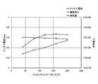
- FIG. 9A is a graph showing the relationship between the capacity Cp, the drive power, the antenna current, and the time difference for the transmission device 10A.
- the drive power here is power supplied to the antenna drive unit (LSI unit 330), and the effective value (or average value) is shown in the graph.
- FIG. 9B is a graph showing the relationship between the capacity Cp, the driving power, the antenna current, and the time difference for the transmission device 10B.
- the driving power here is the power supplied to the booster, and its effective value (or average value) is shown in the graph.
- the driving voltage is different between the transmitting devices 10A and 10B, the voltage is constant in both cases, so that the driving power can be measured by detecting the driving current.
- Tune is mainly to detect the optimum value (optimum control value) of the control signal input to the variable capacitor VC1 for appropriately controlling the resonance frequency.
- the optimum control value varies depending on the environment in which the transmission devices 10A and 10B are used. Therefore, detecting the optimal control value accordingly can appropriately control the resonance frequency of the antenna and lead to obtaining stable communication characteristics.
- FIG. 10 is a graph showing the relationship between the capacitance Cp, the antenna current, and the driving power for various values of matching impedance in the transmission apparatus 10B.
- the solid line indicates the antenna current
- the broken line indicates the drive power.
- the value in () represents the matching impedance ( ⁇ ). That is, the matching impedance was set to 40, 80, 120, 160, and 200 ⁇ . Further, the inductance of the antenna coil L1 was set to 2 ⁇ H.
- the capacitance of the series resonant capacitor is optimized and fixed with each matching impedance.
- the antenna current is maximum under the resonance condition, and the drive power corresponding to the capacitance Cp when the antenna current is maximum is almost equal to the minimum value. Even if the matching impedance is changed, the capacitance Cp in the case where the drive power is minimum is the capacitance corresponding to the resonance frequency. Therefore, the driving power minimum method has an advantage that it is not necessary to consider the matching impedance as compared with the optimum time difference method.
- FIG. 11 is a graph showing the relationship between the capacitance Cp and the time difference for various values of matching impedance in the transmission apparatus 10B.
- the set values of the matching impedance and the antenna coil L1 are the same as in FIG.
- the time difference under the resonance condition increases. Therefore, it is necessary to change the optimum time difference, that is, the optimum phase difference for each matching impedance.
- FIG. 12 is a graph showing the relationship between matching impedance, antenna current, time difference, and driving power in the transmission apparatus 10B.
- the set value of the antenna coil L1 is the same as in FIGS.
- the antenna current increases as the matching impedance increases, but peaks at 160 ⁇ and decreases slightly at 200 ⁇ .
- the time difference increases monotonously and the driving power decreases monotonously, and both may be considered to be almost linear.
- the output impedance of the booster 170 (drive unit thereof) is determined by the inductances of the coils L5 and L6. Therefore, it is considered that the antenna current having a peak under the resonance condition is due to impedance matching with this inductance (1.5 ⁇ H).
- the impedance of the coils L5 and L6 at the resonance frequency of 13.56 MHz is about 130 ⁇ , the current is maximum in this vicinity.
- FIG. 13 is a flowchart showing a tuning method based on the minimum driving power method.
- This minimum drive power method is a method that can be applied to both the transmission apparatuses 100A and 100B.
- the control unit 140 reads the target frequency f0 from the storage unit 145 and sets it in the oscillation unit 131 (step 101). In addition, the control unit 140 sets antenna parameters stored in the storage unit 145 in advance in the internal register of the control unit 140, the gain controller 132, and the like (step 102).
- the antenna parameters are, for example, impedance, Q value, gain of the oscillation signal output from the oscillating unit 131, control voltage value of the DAC 136 as a control signal to the variable capacitor VC1 (eg, 0V as an initial value), and the like.
- Steps 103 to 106 the control unit 140 executes a process for detecting the optimum control value.
- control unit 140 sweeps a control voltage that is a control signal within a predetermined search range (for example, 0 to 3 V). Specifically, the control unit 140 increases the control voltage value to the DAC 136 by, for example, unit voltage from 0V for each step, and measures the drive current by the detection unit 106 for each step, and the drive power Is calculated (step 103). In this case, the control unit 140 functions as an acquisition unit that acquires the drive power value.
- a predetermined search range for example, 0 to 3 V.
- the control unit 140 increases the control voltage value up to 3 V which is the maximum value of the system voltage (until the measurement is completed). Between 0 and 3V (step 106), when the control unit 140 detects the minimum value of the driving power (YES in step 104), it is the optimum control voltage value to the DAC 136 when the driving power is minimum.
- the control value is stored in the storage unit 145 (step 105). In step 105, the measured minimum driving power value may be stored.
- step 103 the control unit 140 specifically compares the value measured last time with the value measured this time. If the value measured this time is smaller than the value measured last time, the control unit 140 sets the value. Just hold it.
- the control unit 140 may acquire the measured drive current value instead of calculating the drive power, and may detect the minimum drive current in step 104.
- the control unit 140 or the ADC 134 functions as an acquisition unit that acquires a drive current value.
- the control unit 140 stores an optimum control value, which is a control voltage value to the DAC 136 when the drive current is minimized, in the storage unit 145.
- the control unit 140 increases the control voltage value to 3V (Yes in Step 106), and then sets a normal communication oscillation frequency (for example, 13.56 MHz) in the oscillation unit 131 (Step 107).
- the control unit 140 sets antenna parameters for communication (step 108) and ends the tuning process.
- One of the communication antenna parameters is an optimal control value stored in the storage unit 145. That is, at the time of communication, the control unit 140 controls the resonance frequency using the optimum control value stored in the storage unit 145.
- FIG. 14 is a flowchart showing a tuning method by the optimum time difference method.
- This optimal time difference method is a method that can be applied to both the transmitting apparatuses 100A and 100B. In this flowchart, the description of the same steps as those shown in FIG. 13 is omitted.
- step 202 the control unit 140 extracts the optimum time difference stored in the storage unit 145, and sets this as one of the antenna parameters.
- the optimal time difference should just be memorize
- the optimum time difference may be calibrated or updated at an arbitrary or predetermined timing after shipment from the factory.
- step 203 the control unit 140 sweeps the control voltage, which is a control signal, within a predetermined search range (for example, 0 to 3 V). Specifically, the control unit 140 increases the unit voltage from 0V step by step, and measures the time difference between the drive pulse (transmission signal) and the antenna current by the measurement unit 105 for each step (step). 203). The control unit 140 acquires the measured time difference, and in this case, functions as an acquisition unit.
- a predetermined search range for example, 0 to 3 V.
- the control unit 140 sets the measured time difference as the optimum time difference. Then, the control unit 140 stores, in the storage unit 145, the optimum control value that is the control voltage value to the DAC 136 when the optimum time difference is detected (step 205).
- the control unit 140 sets the optimum control value stored in step 205 as one of the antenna parameters when setting the antenna parameter for communication in step 108 (step 208).
- the resonance frequency is controlled so that the drive current or the drive power based on the drive current is minimized. Therefore, regardless of the presence or absence of the booster 170, it is possible to appropriately control the resonance frequency of the antenna according to a change in the environment in which the transmission devices 100A and 100B are used, and to obtain stable communication characteristics.
- the minimum driving power method is irrelevant to the matching impedance, so the design is simplified.
- the resonance frequency is controlled so that the drive current or the drive power based on the drive current is minimized by using the optimum time difference between the transmission signal and the antenna current stored in advance. Therefore, similarly to the above, regardless of the presence or absence of the booster 170, it is possible to appropriately control the resonance frequency of the antenna according to the change in the environment in which the transmission device is used, and to obtain stable communication characteristics.
- the same control method can be used regardless of the presence or absence of the booster 170, that is, the transmission devices 100A and 100B. Therefore, the application range is widened, and there are advantages in terms of cost.
- an antenna needs to be arranged in the memory card, but an antenna having a size smaller than the outer shape of the memory card may be mounted. Due to the small size of the antenna, radio waves emitted are weak, and using a small antenna is disadvantageous from the viewpoint of communication. Since it is difficult to reduce the size of the booster to increase the weak radio field intensity, it is difficult to place the booster in the memory card.
- one of the transmission device 100A that does not have the booster 170 and the transmission device 100B that has the booster 170 can be selected and incorporated into the device according to the size of the device.
- Non-contact power supply wireless power supply
- the technology of the contactless communication system 1 can be applied to WPC (Wireless Power Consortium) that is a technology of the contactless power feeding system.
- WPC Wireless Power Consortium
- FIG. 15 is a block diagram showing the configuration of the non-contact power feeding system.
- the difference between this non-contact power feeding system 2 and the non-contact communication system 1 shown in FIG. 1 is that a power feeding mode is provided, and a charging control unit 219 is provided in the power receiving device 250.
- a method corresponding to two-way communication for transmission and reception is shown.
- the antenna resonance unit 110 of the power supply device (transmission device) 150 is configured by an LC resonance circuit, and has an output frequency of 100 to 200 kHz, for example, in the electromagnetic induction method known in the Qi format.
- the oscillation frequency used by the LSI (antenna drive unit) and the specifications of the antenna coil L1 in the antenna resonance unit 110 are different.
- ⁇ As a power feeding method of this non-contact power feeding system 2 a method such as electromagnetic induction or magnetic field resonance can be applied, and it does not depend on the method.
- the power feeding device 150 sends out a carrier signal, and passes a current through the antenna through the primary antenna unit 112.
- a magnetic field generated by a current flowing through the antenna coil is magnetically coupled to the secondary antenna unit 201 of the power receiving apparatus 250, whereby a voltage is excited in the secondary antenna unit 201 and energy is transmitted.
- the communication distance between the transmission device 100 and the reception device 200 is long and the distance changes.
- the power receiving device 250 for example, a mobile phone device
- the power feeding device 150 for example, a power transmission pad
- the distance between the two is always almost constant. It becomes.
- Such a non-contact power feeding system 2 has a resonance circuit in each of the power feeding device 150 and the power receiving device 250, and the problem that the resonance frequency is shifted due to a positional deviation or a device to which power is fed is a problem with the non-contact communication system 1. This is the same as the problem (solved in the non-contact communication system 1).
- the primary side antenna unit 112 and the secondary side antenna unit 201 are configured by a resonance circuit so as to resonate at a carrier frequency in order to perform efficient transmission.
- energy efficiency is determined by multiplying the coupling coefficient k of electromagnetic inductive coupling and the Q value of the antenna, so that a large k and a high Q are desirable.
- the Q of the resonance circuit is increased, the resonance frequency is greatly shifted due to variations in constants. Therefore, it is necessary to use a highly accurate component or adjust the resonance frequency as described above.
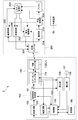
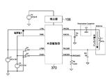
- FIG. 16 shows a circuit configuration of a power feeding device 150 having an external drive unit.
- FIG. 17 shows the configuration of the external drive unit 370.
- the external drive unit 370 is configured as a full bridge circuit.
- the detection unit 106 is configured to detect electric power (current) supplied to the external drive unit 370.
- the technology of the transmission device described above can also be applied to the power supply device of the non-contact power supply system.
- the application of the drive power minimum method or the optimal time difference method allows appropriate control of the antenna resonance frequency according to the fluctuations in the environment in which the power feeding device is used, and stable communication characteristics. Can be obtained.
- a signal from the differential amplifier A2 is input as a transmission signal to the non-inverting input terminal of the phase comparator A3, and an antenna current signal based on the transmission signal is input to the inverting input terminal. It may be input.
- a signal from the differential amplifier A2 is input as a transmission signal to the non-inverting input terminal of the phase comparator A3, and transmission from the differential amplifier A1 is input to the inverting input terminal.
- An antenna current signal may be input as a signal.
- the measuring unit 105 when the tuning is executed only by the minimum driving power method without using the optimal time difference method, the measuring unit 105 may not be provided.
- the detection unit 106 may not be provided.
Landscapes
- Engineering & Computer Science (AREA)
- Computer Networks & Wireless Communication (AREA)
- Signal Processing (AREA)
- Power Engineering (AREA)
- Near-Field Transmission Systems (AREA)
- Transmitters (AREA)
Abstract
【課題】ブースターの有無に関わらず、アンテナの共振周波数に適切に制御でき、これにより安定した通信特性を得ることができる送信装置等の技術を提供すること。 【解決手段】アンテナ共振部110は、アンテナコイルL1と、インピーダンスマッチング部114とを含む。駆動部(例えばアンテナ駆動部130)は、アンテナ共振部110への送信信号を生成する。検出部106は、駆動部が動作するための駆動電流または駆動電力を検出する。制御部140は、インピーダンスマッチング部114を制御する制御信号を生成可能であり、制御信号のうち、検出部106で検出された駆動電流または駆動電力が最小となる最適制御値を使用して、アンテナ共振部110の共振周波数を制御する。
Description
本発明は、電磁結合により非接触通信または非接触給電を行う送信装置等の技術に関する。
近年、近距離における非接触通信技術であるNFC(Near Field Communication)を利用した非接触通信システムの普及が著しい。NFCは、クレジットカード、電子マネー、電子乗車券、IDカード、貨物管理用タグ、メモリカード、非接触式電力伝送システムなどに、広く利用されている。このような非接触通信システムでは、システム専用のリーダ/ライタ(以下、R/Wと記す)装置の送信アンテナ(共振回路)から出力された送信信号を、非接触IC(Integrated circuit)カード内に設けられた受信アンテナが電磁誘導作用により受信する。
このような非接触通信システムでは、安定した通信特性を得るためには、R/W装置内の信号源の周波数と、R/W装置の送信アンテナの共振周波数と、非接触ICカード内の受信アンテナ(共振回路)の共振周波数とが互いに一致することが重要である。しかしながら、非接触ICカードの受信アンテナまたはR/W装置の送信アンテナの共振周波数は、R/W装置が使用される環境等、様々な要因により変動する。この場合、非接触ICカードおよびR/W装置間で安定して情報を送受信することが困難になる。
そこで、非接触通信システムの技術分野では、あらゆる条件下において、安定した通信状態を保つための様々な技術が提案されている。例えば特許文献1の非接触通信装置では、アンテナ駆動部(例えばLSI)では、差動増幅器でなる測定部が、発振部からの出力電流(LSIによる駆動電流)を測定する。そして、制御部が、その出力電流の最小値または最大値を検出し、それら最小値または最大値に対応する最適制御値を使用して共振周波数を制御している(特許文献1の[要約]に記載)。
ところで、例えば非接触式の通信装置では、パワー不足による通信エラーが発生することがある。そこで、通信パワーの増幅のためにブースターが設けられる場合がある。
例えば、特許文献2では、ブースターを用いることの必要性が述べられている。非接触型のRFID R/Wと、RFIDタグとの通信距離は、数cmである。しかし、上述のように、種々の用途が考えられるRFIDシステムでは、多様な用途が考えられ、適用分野によっては、通信距離をさらに延長できることが望ましい。これに対処するため、RFIDタグとRFIDリーダライタとの間に、ブースターアンテナを配置することが提案されている(特許文献2の明細書段落[0005]記載)。
特許文献3では、小型のアンテナでも通信距離を確保するためにブースターを設けることが開示されている。また、この特許文献3では、NFCコントローラと接続された検波回路が当該NFCコントローラからの入力信号に基づき検波信号を生成し、検波信号により起動した電源がブースターに電力を供給する。これにより、非通信状態では、ブースターが動作しないため、無線通信装置の消費電力を抑えることができる(特許文献3の明細書段落[0005]、[0016]、[0019]、[0025]記載)。
ブースターアンテナコイルを、メモリカードなど小型の送信機内に搭載することは難しい。また、ブースターの有無に関わらず、様々な環境の中で、適切な共振周波数に制御されることが要求される。
本発明の目的は、ブースターの有無に関わらず、アンテナの共振周波数に適切に制御でき、これにより安定した通信特性を得ることができる送信装置等の技術を提供することにある。
上記目的を達成するため、本発明の一形態に係る送信装置は、アンテナ共振部と、駆動部と、検出部と、制御部とを含む。
前記アンテナ共振部は、アンテナコイルと、インピーダンスマッチング部とを含む。
前記駆動部は、前記アンテナ共振部への送信信号を生成する。
前記検出部は、前記駆動部が動作するための駆動電流または駆動電力を検出する。
前記制御部は、前記インピーダンスマッチング部を制御する制御信号を生成可能であり、前記制御信号のうち、前記検出部で検出された駆動電流または駆動電力が最小となる最適制御値を使用して、前記アンテナ共振部の共振周波数を制御する。
前記アンテナ共振部は、アンテナコイルと、インピーダンスマッチング部とを含む。
前記駆動部は、前記アンテナ共振部への送信信号を生成する。
前記検出部は、前記駆動部が動作するための駆動電流または駆動電力を検出する。
前記制御部は、前記インピーダンスマッチング部を制御する制御信号を生成可能であり、前記制御信号のうち、前記検出部で検出された駆動電流または駆動電力が最小となる最適制御値を使用して、前記アンテナ共振部の共振周波数を制御する。
このような構成によれば、駆動部が動作するための駆動電流、またはその駆動電流に基づく駆動電力が最小になるように共振周波数が制御されるので、ブースターの有無に関わらず、送信装置が使用される環境の変動に応じて、アンテナの共振周波数に適切に制御でき、安定した通信特性を得ることができる。
前記制御部は、所定のサーチ範囲内で前記制御信号を出力することにより、前記最適制御値を検出するように構成されていてもよい。
前記検出部は、前記駆動電流の平均値または実効値を出力するように構成されていてもよい。
前記送信装置は、前記駆動電流または前記駆動電力が最小となるときの前記インピーダンスマッチング部における被制御量に対応する最適な時間差であって、前記送信信号と前記アンテナコイルに流れるアンテナ電流との最適時間差を記憶する記憶部をさらに具備してもよい。
これにより、制御部は、最適時間差に基づき、その最適時間差に対応する最適制御値を用いて、共振周波数を制御することができる。
これにより、制御部は、最適時間差に基づき、その最適時間差に対応する最適制御値を用いて、共振周波数を制御することができる。
前記送信装置は、前記送信信号と前記アンテナコイルに流れるアンテナ電流との時間差を測定する測定部をさらに具備してもよい。
前記制御部は、所定のサーチ範囲内で前記制御信号を出力することにより、前記測定部で測定された時間差を取得し、その測定された時間差と、前記最適時間差との比較結果に基づき、前記最適制御値を検出するように構成されていてもよい。
これにより、送信装置は、環境の変動に対応した最適制御値を使用することができる。
これにより、送信装置は、環境の変動に対応した最適制御値を使用することができる。
前記測定部は、前記駆動部から出力され前記アンテナ共振部へ入力される前記送信信号の位相と、前記アンテナ電流の位相とを比較する位相比較器を有する。
前記駆動部は、発振部と、前記発振部からの信号が入力され、前記送信信号として、第1信号および前記第1信号の位相とは逆位相の第2信号をそれぞれ生成する一対の差動増幅器とを有していてもよい。
前記位相比較器は、前記一対の差動増幅器がそれぞれ生成する信号のうち前記第1信号の位相と、前記第1信号による前記アンテナ電流の位相とを比較するように構成されていてもよい。
前記位相比較器は、前記一対の差動増幅器がそれぞれ生成する信号のうち前記第1信号の位相と、前記第1信号による前記アンテナ電流の位相とを比較するように構成されていてもよい。
前記駆動部は、前記アンテナ電流の増幅する外部駆動部と、発振部と、前記発振部からの信号が入力され、前記送信信号として、第1信号および前記第1信号の位相とは逆位相の第2信号をそれぞれ生成する一対の差動増幅器とを有していてもよい。
前記位相比較器は、前記一対の差動増幅器がそれぞれ生成する信号のうち前記第1信号の位相と、前記第2信号による前記アンテナ電流の位相とを比較するように構成されていてもよい。
前記位相比較器は、前記一対の差動増幅器がそれぞれ生成する信号のうち前記第1信号の位相と、前記第2信号による前記アンテナ電流の位相とを比較するように構成されていてもよい。
前記駆動部は、前記アンテナ電流の増幅する外部駆動部を有していてもよい。
本発明の他の形態に係る送信装置は、上記したアンテナ共振部と、上記した駆動部と、測定部と、制御部とを具備する。
前記測定部は、前記送信信号と前記アンテナコイルに流れるアンテナ電流との時間差を測定する。
前記制御部は、前記インピーダンスマッチング部を制御する制御信号を生成可能であり、前記制御信号のうち最適制御値を使用して、前記アンテナ共振部の共振周波数を制御する。前記最適制御値は、前記測定部により測定された時間差のうち、前記駆動部が動作するための駆動電流または駆動電力が最小となるときの最適時間差に対応する値である。
前記測定部は、前記送信信号と前記アンテナコイルに流れるアンテナ電流との時間差を測定する。
前記制御部は、前記インピーダンスマッチング部を制御する制御信号を生成可能であり、前記制御信号のうち最適制御値を使用して、前記アンテナ共振部の共振周波数を制御する。前記最適制御値は、前記測定部により測定された時間差のうち、前記駆動部が動作するための駆動電流または駆動電力が最小となるときの最適時間差に対応する値である。
このような構成によれば、最適時間差を使用して、駆動部が動作するための駆動電流、またはその駆動電流に基づく駆動電力が最小となるように共振周波数が制御されるので、ブースターの有無に関わらず、アンテナの共振周波数に適切に制御でき、安定した通信特性を得ることができる。
本発明の一形態に係るアンテナ駆動装置は、アンテナコイルと、インピーダンスマッチング部とを含むアンテナ共振部を駆動するアンテナ駆動装置であって、生成部と、取得部と、制御部とを具備する。
前記生成部は、前記アンテナ共振部への送信信号を生成する。
前記取得部は、前記駆動部が動作するための駆動電流または駆動電力を検出する検出部により検出された前記駆動電流の値を取得する。
前記制御部は、前記インピーダンスマッチング部を制御する制御信号を生成可能であり、前記制御信号のうち、前記検出部で検出された駆動電流または駆動電力が最小となる最適制御値を使用して、前記アンテナ共振部の共振周波数を制御する。
前記生成部は、前記アンテナ共振部への送信信号を生成する。
前記取得部は、前記駆動部が動作するための駆動電流または駆動電力を検出する検出部により検出された前記駆動電流の値を取得する。
前記制御部は、前記インピーダンスマッチング部を制御する制御信号を生成可能であり、前記制御信号のうち、前記検出部で検出された駆動電流または駆動電力が最小となる最適制御値を使用して、前記アンテナ共振部の共振周波数を制御する。
本発明の他の形態に係るアンテナ駆動装置は、アンテナコイルと、インピーダンスマッチング部とを含むアンテナ共振部を駆動するアンテナ駆動装置であって、上記した生成部と、取得部と、制御部とを具備する。
前記取得部は、前記送信信号と前記アンテナコイルに流れるアンテナ電流との時間差を測定する測定部により測定された前記時間差を取得する。
前記制御部は、前記インピーダンスマッチング部を制御する制御信号を生成可能であり、前記制御信号のうち最適制御値を使用して、前記アンテナ共振部の共振周波数を制御する。前記最適制御値は、前記測定部により測定された時間差のうち、前記駆動部が動作するための駆動電流または駆動電力が最小となるときの最適時間差に対応する値である。
前記取得部は、前記送信信号と前記アンテナコイルに流れるアンテナ電流との時間差を測定する測定部により測定された前記時間差を取得する。
前記制御部は、前記インピーダンスマッチング部を制御する制御信号を生成可能であり、前記制御信号のうち最適制御値を使用して、前記アンテナ共振部の共振周波数を制御する。前記最適制御値は、前記測定部により測定された時間差のうち、前記駆動部が動作するための駆動電流または駆動電力が最小となるときの最適時間差に対応する値である。
本発明の一形態に係るチューニング方法は、上記したアンテナ共振部と、上記した駆動部とを備える送信装置による、前記アンテナ共振部の共振周波数のチューニング方法である。
前記インピーダンスマッチング部を制御する制御信号が出力される。
前記制御信号の出力に応じて前記駆動部が動作するための駆動電流または駆動電力が検出されることで、前記制御信号のうち、前記駆動電流または前記駆動電力が最小となる最適制御値が検出される。
前記インピーダンスマッチング部を制御する制御信号が出力される。
前記制御信号の出力に応じて前記駆動部が動作するための駆動電流または駆動電力が検出されることで、前記制御信号のうち、前記駆動電流または前記駆動電力が最小となる最適制御値が検出される。
本発明の他の形態に係るチューニング方法は、上記したアンテナ共振部と、上記した駆動部とを備える送信装置による、前記アンテナ共振部の共振周波数のチューニング方法である。
前記インピーダンスマッチング部を制御する制御信号が出力される。
前記制御信号の出力に応じて前記送信信号と前記アンテナコイルに流れるアンテナ電流との時間差が測定される。
測定された時間差と、前記駆動部が動作するための駆動電流または駆動電力が最小となるときの前記インピーダンスマッチング部における被制御量に対応する最適な時間差であって、前記送信信号と前記アンテナコイルに流れるアンテナ電流との最適時間差とが比較されることで、前記制御信号のうち、前記駆動電流または前記駆動電力が最小となる最適制御値が検出される。
前記インピーダンスマッチング部を制御する制御信号が出力される。
前記制御信号の出力に応じて前記送信信号と前記アンテナコイルに流れるアンテナ電流との時間差が測定される。
測定された時間差と、前記駆動部が動作するための駆動電流または駆動電力が最小となるときの前記インピーダンスマッチング部における被制御量に対応する最適な時間差であって、前記送信信号と前記アンテナコイルに流れるアンテナ電流との最適時間差とが比較されることで、前記制御信号のうち、前記駆動電流または前記駆動電力が最小となる最適制御値が検出される。
上記チューニング方法を実行する送信装置のプログラムも提供され得る。
以上、本発明によれば、ブースターの有無に関わらず、アンテナの共振周波数に適切に制御でき、これにより安定した通信特性を得ることができる。
以下、図面を参照しながら、本発明の実施形態を説明する。
1.非接触通信システム
1.1)非接触通信システムの構成
図1は、本発明の一実施形態に係る非接触通信システムの構成を示すブロック図である。なお、図1では、各回路ブロック間において情報の入出力に関する配線を実線矢印で示し、電力の供給に関する配線を破線矢印で示す。
本発明の一実施形態に係る非接触通信システム1は、国際標準規格ISO/IEC18092を基礎とするNFC-A、NFC-B、NFC-F等を含む近距離無線通信技術であるNFC(Near Field Communication)に適用される。
非接触通信システム1は、送信装置100と、受信装置200とを備える。非接触通信システム1は、送信装置100と受信装置200との間で非接触通信により情報の送受信を行う。なお、非接触通信システム1の例としては、例えば、Felica(登録商標)に代表されるような非接触ICカード規格と、NFC規格とを組み合わせた通信システムが挙げられる。
1.2)送信装置
送信装置100について説明する。送信装置100は、受信装置200に対して非接触でデータを読み書きするリーダ/ライタ(R/W)機能を有する装置である。送信装置100は、図1に示すように、アンテナ共振部110、アンテナ駆動部130(駆動部、アンテナ駆動装置)(図2参照)、検出部106、および記憶部145を備える。
図1に示すようにアンテナ共振部110は、1次側アンテナ部112およびインピーダンスマッチング部114を有し、後述するように、アンテナコイルL1および共振コンデンサ(可変容量コンデンサ)を備える共振回路を構成する。アンテナ共振部110は、受信装置200の2次側アンテナ部201との間で、電磁結合により信号を送受信する。
1次側アンテナ部112は、共振回路により所望の周波数の送信信号を送信すると共に、受信装置200からの応答信号を受信する機能を有する。
インピーダンスマッチング部114は、アンテナ駆動部130の送信信号生成部(生成部)101と1次側アンテナ部112との間のインピーダンスの整合を取るマッチング回路としての機能を有する。本実施形態では、後述するように、アンテナ駆動部130の制御部が、後述するようにインピーダンスマッチング部114を制御することにより、送信信号生成部101と1次側アンテナ部112との間のインピーダンスマッチングおよび共振周波数の最適化を実現する。
アンテナ駆動部130は、主に、送信信号生成部101、変調回路102、復調回路103、および制御部140を有する。
送信信号生成部101は、変調回路102から入力された送信データにより所望の周波数(例えば13.56MHz)のキャリア信号を変調し、インピーダンスマッチング部114を介して、当該変調したキャリア信号を1次側アンテナ部112に出力する機能を有する。
変調回路102は、制御部140から入力された送信データを符号化し、当該符号化した送信データを送信信号生成部101に出力する機能を有する。
復調回路103は、1次側アンテナ部112で受信した応答信号をインピーダンスマッチング部114を介して取得し、該応答信号を復調する機能を有する。そして、復調回路103は、復調した応答データを制御部140に出力する機能を有する。
制御部140は、外部からの指令や内蔵するプログラムにしたがって、各種制御用の指令信号を生成し、該指令信号を変調回路102に出力して、回路の動作を制御する機能を有する。また、制御部140は、指令信号に対応した送信データを生成し、該送信データを変調回路102に供給する機能を有する。さらに、制御部140は、復調回路103で復調された応答データに基づいて所定の処理を行う機能を有する。
具体的には、制御部140は、送信装置100のR/W機能とカード機能を制御する機能を有する。R/W機能は、送信装置100が、2次側機器(相手側機器)である受信装置200と通信(データの読み書き)を行う機能である。カード機能とは、図1に示した2次側機器である受信装置200の機能であり、送信装置100が、その機能を持つことを意味する。
また、制御部140は、インピーダンスマッチング部114を制御する制御信号(例えば制御電圧)を生成し、これをインピーダンスマッチング部114に出力する。インピーダンスマッチング部114は、後述するように可変コンデンサ(可変容量コンデンサ)を備え、制御信号により可変コンデンサの容量(被制御量)が制御される。これにより、アンテナ共振部110の共振周波数が制御される。
なお、制御部140は、送信装置100のシステム全体を制御する制御部と、信号の送受信を制御する送受信制御部とに、機能的または物理的に分かれていてもよい。この場合、送受信制御部が、主に上記のインピーダンスマッチング部114の制御を実行するように構成される。
制御部140は、例えば主にCPU(Central Processing Unit)および/またはPLD(Programmable Logic Device)により構成される。
検出部106は、アンテナ駆動部130に接続された電源107から供給される電流を検出する機能を有する。この電流は、アンテナ駆動部130(および/または後述するブースター)が動作するための駆動電流である。
1.3)受信装置
次に、受信装置200について説明する。なお、図1に示す例では、受信装置200を非接触ICカードとして動作するモバイル機器で構成した例を示す。また、この例では、受信装置200が、自身の共振周波数を制御する機能を備える例を説明する。
受信装置200は、図1に示すように、受信アンテナとしての機能を有する2次側アンテナ部201、整流部204、受信制御部202、復調回路205、システム制御部203、変調回路206、定電圧部207、バッテリー208を備える。
2次側アンテナ部201は、例えば不図示の共振コイルおよび複数の共振コンデンサからなる共振回路を有している。この共振コンデンサは、制御電圧を印加することにより容量が変化する可変コンデンサを含む構成となっている。2次側アンテナ部201は、送信装置100の1次側アンテナ部112と電磁結合により通信を行い、1次側アンテナ部112が発生する磁界を受けて、送信装置100からの送信信号を受信する機能を有する。この際、2次側アンテナ部201の共振周波数が所望の周波数となるように、可変コンデンサの容量が制御される。
整流部204は、例えば、整流用ダイオードと整流用コンデンサとからなる半波整流回路で構成され、2次側アンテナ部201で受信した交流電力を直流電力に整流し、当該整流した直流電力を定電圧部207に出力する機能を有する。
定電圧部207は、整流部204から入力された電気信号(直流電力)に対して電圧変動(データ成分)の抑制処理および安定化処理を施し、当該処理された直流電力を受信制御部202に供給する機能を有する。なお、整流部204および定電圧部207を介して出力された直流電力は、受信装置200内のICを動作させるための電源として使用される。
受信制御部202は、2次側アンテナ部201の共振特性を制御して、受信時における共振周波数の最適化を図る機能を有する。具体的には、2次側アンテナ部201内に含まれる可変コンデンサに制御電圧を印加してその容量を制御し、これにより、2次側アンテナ部201の共振周波数を制御する。
復調回路205は、2次側アンテナ部201で受信した受信信号を復調し、当該復調した信号をシステム制御部203に出力する機能を有する。
システム制御部203は、復調回路205で復調された信号に基づいて、その内容を判断して必要な処理を行い、変調回路206および受信制御部202を制御する機能を有する。
変調回路206は、システム制御部203で判断された結果(復調信号の内容)に従って受信キャリアを変調して応答信号を生成する機能を有する。また、変調回路206は、生成した応答信号を2次側アンテナ部201に出力する機能を有する。変調回路206から出力された応答信号は、非接触通信により、2次側アンテナ部201から1次側アンテナ部112に送信される。
バッテリー208は、システム制御部203に電力を供給する機能を有する。このバッテリー208への充電は、その充電端子を外部電源50に接続することにより行われる。図1に示す例のように、受信装置200がバッテリー208を内蔵する構成である場合には、より安定した電力をシステム制御部203に供給することができ、安定した動作が可能となる。
なお、受信装置200は、バッテリー208を使用せずに、整流部204および定電圧部207を介して生成される直流電力を用いて、システム制御部203を駆動する構成であってもよい。
本実施形態の非接触通信システム1では、送信装置100の1次側アンテナ部112と受信装置200の2次側アンテナ部201との間において、電磁結合を介して非接触でデータ通信が行われる。このため、送信装置100および受信装置200において効率良く通信を行うために、1次側アンテナ部112および2次側アンテナ部201の各共振回路が同じキャリア周波数(例えば13.56MHz)で共振するように構成される。
2.送信装置の回路構成
2.1)ブースター(外部駆動部)を持たない送信装置
図2は、図1に示した送信装置100として、ブースターを持たない送信装置100Aの回路構成を示す。ブースターを持たない送信装置100Aでは、アンテナ駆動部130が「駆動部」として機能する。
アンテナ共振部110は、アンテナコイルL1およびこれに接続されたインピーダンスマッチング部114を有する。インピーダンスマッチング部114は、アンテナ駆動部130とアンテナコイルL1のインピーダンス不整合を防ぎ、アンテナ駆動部130の負荷(インピーダンス)をアンテナコイルL1によらず常に一定、かつ純抵抗としている。
例えばアンテナ共振部110は、アンテナコイルL1に、可変コンデンサ(並列共振コンデンサ)VC1が並列接続され、また、固定容量のコンデンサC2、C5(直列共振コンデンサ)が直列接続された直並列共振回路として構成される。可変コンデンサVC1は、これに入力される制御電圧(制御信号)が変化することにより、容量が変化し、これにより、アンテナ共振部110の共振周波数が変化する。なお、可変コンデンサは、複数設けられ、それら複数の可変コンデンサの容量が、同じ制御電圧値により変化するように構成されていてもよい。
コンデンサC9、C10(並列共振コンデンサ)は、アンテナサイズの違い等によるアンテナ特性差を吸収するための追加のコンデンサである。コンデンサC9、C10の容量をそれぞれCp2とし、可変コンデンサVC1の容量をCp1とすると、これらの合成容量はCp1+Cp2/2となる。可変容量コンデンサVC1は、印加される制御電圧が大きくなると容量が減少するように構成されている。したがって、制御電圧が大きくなると共振周波数は高くなる。
コンデンサC7、C8は、可変コンデンサVC1に印加される上記制御電圧(DC電圧)がアンテナL3に漏れないようにするためのDCカットの機能を有する。コンデンサC7、C8の容量は、後述するチューニングの実行時での影響を小さくするため、合成容量(Cp1+Cp2/2)としての例えば200pFに比べ、十分に大きな10nFに設定されている。コンデンサC7、C8の容量が小さい場合、可変コンデンサVC1の可変率が減少する等の影響が出てくる。
インピーダンスマッチング部114は、アンテナ共振部110のQ値(Quality Factor、先鋭度)を決めるダンピング抵抗R5、R6を有する。本実施形態では、これらはショート抵抗(0Ω)とされる。
フィルタ部120は、コイルL2、L3、コンデンサC1、C4を有し、EMC(Electro Magnetic Compatibility)機能を有する。アンテナ駆動部130から出力される高周波の発振信号(上記送信信号)は矩形波である。フィルタ部120は、この発振信号による高周波ノイズを除去する機能を有する。そのカットオフ周波数は16MHz~20MHzとされる。コイルL2、L3は、コンデンサC2、C5の一方の端子にそれぞれ接続されている。コンデンサC1、C4は、コイルL2、L3のそれぞれとグランドとの間に接続されている。
アンテナ駆動部130の送信信号生成部101は、発振周波数を制御可能な発振部131と、発振部131により得られる発振信号をアンテナ共振部110に供給するパルス発生部135と、発振部131の出力ゲインを制御するゲインコントローラ132とを備える。パルス生成部135は駆動部としても機能する。
発振部131は、12MHz~17MHzの広範囲に亘る発信周波数の信号を出力するように制御部140により制御される周波数可変発振器からなる。典型的には、発振周波数は、13.56MHzに制御されるが、設計上、13.56MHzからオフセットされた発振周波数に制御される場合もある。そのオフセットされた発振周波数は、メーカーや製品モデルによって異なる固有値である。
制御部140は、発振部131によって出力される発振周波数を、ターゲット周波数f0(上述した13.56MHz、または、それからオフセットされた発振周波数)に一致させるように制御する。
本実施形態では、上記ターゲット周波数f0は、アンテナ共振部110のインダクタンス、Q値、インピーダンス等の設計により決まる設計値である。これらはアンテナ特性を決定する設計値である。
パルス発生部135は、発振部131から供給される高周波の発振信号を、正相のパルス信号(例えば第1信号)と、それと逆位相のパルス信号(例えば第2信号)を生成し、これらを送信信号としてフィルタ部120に出力する。例えば、パルス発生部135は、これらの2つの信号をそれぞれ生成する一対の差動増幅器A1、A2を含む。
アンテナ駆動部130は、制御部140からのデジタルの制御電圧値を、アナログ信号に変換するDAC(デジタル/アナログ変換器)136を有する。DAC136によって変換されたアナログのバイアス制御電圧は、可変コンデンサVC1に印加される。また、アンテナ駆動部130は、検出部106で検出された電流値を示すDC電圧信号をデジタル化するADC(アナログ/デジタル変換器)134を有する。
アンテナ駆動部130は、パルス発生部135の送信信号と、アンテナ部を流れる電流であるアンテナ電流との時間差を測定する測定部105を有する。例えば測定部105は、位相比較器A3と、ディレイ算出部108とを有する。Tx1端子およびTx2端子からそれぞれ出力される信号でなる送信信号により、アンテナコイルL1にアンテナ電流が流れる。そのアンテナ電流の位相を、アンテナコイルL1の両端に接続されたRx1端子(あるいは、後述する送信装置100BではRx2端子)を利用して、アンテナ駆動部130内に取り込むことができる。
例えば、位相比較器A3の非反転入力端子には、送信信号として差動増幅器A1からの信号が入力される。反転入力端子には、送信信号によるアンテナ電流(インピーダンスマッチング部114において、送信信号が供給される線を流れる電流)の信号が入力される。位相比較器A3は、これらの信号の位相を比較して位相差に相当する電圧信号を出力するように構成される。ディレイ算出部108はその位相差に基づき、その時間差を算出し、これを制御部140に出力する機能を有する。
測定部105は、アンテナ駆動部130の外部に設けられていてもよい。
送信装置100Aは、アンテナパラメータ、発振部131による発振周波数等の設定値、上記時間差等を記憶する記憶部145を備える。
アンテナ駆動部130は、例えばLSI(Large Scale Integration)により構成される。検出部106および記憶部145のうち少なくとも1つは、このLSIの内部に設けられていてもよい。また、制御部140を構成する回路のうち一部または全部が、このLSI(アンテナ駆動部130)の外部に設けられていてもよい。
R/W機能を実現するためのRWモードでは、制御部140は、発振部131を上記した周波数範囲のうち任意の周波数で発振させ、パルス発生部135がその周波数を持つ信号をTx1端子およびTx2端子にそれぞれ出力するように、制御を実行する。一方、カード機能を実現するためのカードモードでは、制御部140は、アンテナ共振部110のアンテナコイルL1に誘起される受信信号を図示しない受信回路で検出し、負荷変調により応答する制御を行う。
2.2)ブースター(外部駆動部)を持つ送信装置
図3は、図1に示した送信装置100として、ブースターを持つ送信装置100Bの回路構成を示す。これ以降の説明では、図2に示した形態に係る送信装置が含む要素や機能等について実質的に同様の要素については同一の符号を付し、その説明を簡略化または省略し、異なる点を中心に説明する。
この送信装置100Bでは、アンテナ駆動部130とフィルタ部120との間に接続されたブースター170を備える。ブースターを持つ送信装置100Bでは、主にブースター170が「駆動部」として機能する。ブースター170は、アンテナ駆動部130からの出力電圧を増幅させることにより、アンテナ電流の振幅を増大させる機能を有する。
図2に示した送信装置100Aにおけるパルス発生部135への電力供給ライン(VC1_driveのライン)とは別の電力供給ライン(VC2_driveのライン)が、検出部106を介してブースター170に接続されている。すなわち、検出部106は、ブースター170に供給される電力(電流)を検出する。
図2に示した送信装置100Aでは、上述したように、測定部105における位相比較器A3の反転入力端子には、差動増幅器A1が生成する信号によるアンテナ電流の信号Rx1が入力された。これに対し、この送信装置100Bでは、位相比較器A3の反転入力端子には、パルス発生部135における差動増幅器A2が生成する信号によるアンテナ電流(インピーダンスマッチング部114において、当該差動増幅器A2が生成する信号が供給される線を流れる電流)の信号Rx2が入力される。この違いの意味については後述する。
3.本実施形態に係る送信装置(図1、2)の動作を理解するための参考例
3.1)参考例に係る信号装置の構成
図4は、参考例に係る、ブースターを持たない送信装置の基本的な回路構成を示す。この送信装置10Aは、LSI部330(アンテナ駆動部)、フィルタ部320、インピーダンスマッチング部314、およびアンテナコイルL1を備える。インピーダンスマッチング部314は、固定容量の、直列共振のコンデンサC2、C5、並列共振のコンデンサC9、C10を有する。
図5は、参考例に係る、ブースター170を持つ送信装置の基本的な回路構成を示す。この送信装置10Bは、図4に示した送信装置10Aにおいて、LSI部330とフィルタ部320との間にブースター170が挿入されたものである。このブースター170は、例えば決済端末で使用される回路である。
ブースター170は、トランジスタQ1、Q2、コイルL5、L6により電圧増幅を行う。駆動電圧は、例えば5Vとされる。トランジスタQ1、Q2が、コイルL5、L6に流れるそれぞれの電流をON/OFFすることで、駆動電圧5Vより高い電圧を発生させ、駆動電流を増大させる。
コイルL5、L6による位相遅れを補正して、ブースター170による位相変化をほぼゼロにするために、コンデンサC13、C14の容量は、ωL=1/ωCを満たすように設定されている。ブースター170での位相変化は、コイルL5およびコンデンサC1で相殺されるため、インピーダンスマッチング部314の各コンデンサC2、C5、C9、C10の容量は、ブースター170の有無に関わらず同じ値を使用できる。実際には、LSI部330の出力インピーダンスの影響やコンデンサC13による位相補正ずれが生じるため、図8の表に示すように、並列共振コンデンサC9、C10、直列共振コンデンサC2、C5の容量の最適化が図られている。
図3に示した送信装置100Bにおけるブースター170は、図5に示したブースター170と同様の構成を有する。
3.2)駆動パルスおよびアンテナ電流の時間差
図6A~Cは、図4に示した参考例に係る送信装置10Aにおいて、共振条件(コンデンサC2、C5、C9、C10が最適化された状態)での各部の信号の計算結果を示すグラフである。具体的には、図6Aは、LSI部330における抵抗R1を流れる電流であり、LSI部330が動作するための駆動電流を示す。図6Bは、アンテナコイルL1を流れるアンテナ電流を示す。図6Cは、電源V1、V2による駆動パルスを示す。
なお、図1に示した電源107により供給される電力に相当する電力が、図4に示した電源V1、V2から供給される電力の一部に相当する(図2の「VC1_drive」)。
このような共振条件において、駆動パルス(つまり送信信号)およびアンテナ電流の時間差を求めることを考える。そのためには、駆動パルスおよびアンテナ電流のそれぞれの位相基準点を考慮する必要がある。
この送信装置10Aにおいて、駆動パルスは、電圧V1、V2の位相が180°ずれた(極性が反転した)2つのパルスで駆動する差動回路により生成される。駆動パルスは、VP、VNの差信号であるため、-3~+3Vの6Vppとなる。駆動パルスの位相基準点は、0Vとなる点であり、駆動パルスの立ち上がりタイミングt1である。
送信装置10Aは、コイルを含む回路を駆動するため、駆動電流は正弦波ではなく歪が生じる。駆動電流の位相基準点は、0mAとなる点である。これに対し、アンテナ電流は13.56MHzの共振回路となっているため、綺麗な正弦波となっており、アンテナ電流の位相基準点の0mAは容易に求められる。
このような共振条件において、駆動パルスの位相基準点、つまり駆動パルスの立ち上がりタイミングt1から、アンテナ電流の位相基準点のタイミングt2までの時間差は、14.9nsとなった。この時間差(t2-t1)に相当する位相差は、当該時間差14.9nsと周波数13.56MHzから算出することができる。
図7A~Cは、図5に示した参考例に係る送信装置10Bにおいて、共振条件(コンデンサC2、C5、C9、C10が最適化された状態)での各部の信号を示すグラフである。具体的には、図7Aは、LSI部330における抵抗R1を流れる電流である。図7Bは、ブースター170のコイルL5に流れる電流であり、駆動電流(例えば駆動電圧5Vによる電源電流)を示す。図7Cは、アンテナ電流を示し、図7Dは、電源V1、V2による駆動パルスを示す。
なお、図1に示した電源107により供給される電力に相当する電力が、図4に示した電源V0から供給される電力の一部に相当する(図3の「VC2_drive」)。
この送信装置10Bについても、上記送信装置10Aの場合と同様に、駆動パルス(つまり送信信号)およびアンテナ電流の時間差を求めることを考える。
この送信装置10Bにおいて、ブースター170のコイルL5、L6によるブースト効果により、図7Bに示したように駆動電流に大きな歪が生じていること、また、その駆動電流の位相基準点が判然としないことがわかる。
図7Aに示すように、図6Aの駆動電流に相当する、LSI部330の出力電流は、トランジスタQ1、Q2のみを駆動すればよいため、パルス的な駆動電流となり、電流値が小さくなっていること、連続波でなく歪が多いことがわかる。したがって、このLSI部330の出力電流の電流検出を行うことは容易ではない(不向きである)ことがわかる。
図7Cに示すように、アンテナ電流はブースター170によりインピーダンスZが同じ80Ωであるにも関わらず、図6Bに示したアンテナ電流に比べ、振幅が1.7倍に増えているのがわかる。
送信装置10Bでは、LSI部330から出力されたパルス信号は、トランジスタQ1、Q2によって反転する。したがって、アンテナ電流の位相基準点は、図7Dにおいてタイミングt2で示す立ち下がりエッジから、タイミングt4で示す立ち上がりエッジへシフト(反転)される必要がある。つまり、位相基準点は、駆動パルスの半周期分シフトされる必要がある。
この場合、駆動パルスとアンテナ電流の位相基準点同士の時間差は、駆動パルスの立ち上がりエッジのタイミングt3から、アンテナ電流の位相基準点(立ち上がりから0mAになる点)のタイミングt4までとなる。当該時間差(t4-t3)は、17.7nsとなった。
駆動パルスの立ち下がりのタイミングt1から、アンテナ電流の位相基準点(立ち下がりから0mAになる点)のタイミングt2までの時間差も、同じ17.7nsである。
この送信装置10Bでの時間差(17.7ns)は、トランジスタQ1により時間遅れや、コンデンサC13による位相補正ずれのため、送信装置10Aでの時間差(14.9ns)に比べ、約3ns大きな値となった。
上記位相基準点のシフトあるいはエッジの反転を実現するために、図3に示したように、送信装置10Bにおける位相比較器A3の反転入力端子に入力される信号は、送信装置10Aにおける位相比較器A3の反転入力端子に入力される信号と異なっている(180°シフトあるいは反転されたものとなってる)。
3.3)共振条件
図8は、送信装置10A、10Bについて、共振条件をまとめた表である。具体的には、マッチングインピーダンス、並列共振コンデンサC9、C10の容量(Cp)、直列共振コンデンサC2、C5の容量(Cs)、アンテナ電流、時間差を示す。
図9Aは、送信装置10Aについて、容量Cpと、駆動電力、アンテナ電流、および時間差との関係を示すグラフである。ここでの駆動電力とは、アンテナ駆動部(LSI部330)に供給される電力であり、グラフではその実効値(あるいは平均値)を示す。
図9Bは、送信装置10Bについて、容量Cpと、駆動電力、アンテナ電流、および時間差との関係を示すグラフである。ここでの駆動電力とは、ブースターに供給される電力であり、グラフではその実効値(あるいは平均値)を示す。
図9Aに示すように、容量Cpが大きくなると(共振周波数が低くなると)、時間差は大きくなり、アンテナ電流は低くなる。駆動電力は共振条件となるCp=116pFで最小となることがわかる。つまり、共振条件では、アンテナ電流を最も効率的に駆動できていることになる。容量Cpが大きいとアンテナ電流が減ってしまう理由は、共振周波数ずれによってインピーダンスZが80Ωより大きくなるためである。
図9Bに示すように、容量Cpが大きくなると(共振周波数が低くなると)、図9Aと同様に、時間差は大きくなるが、アンテナ電流は、共振条件のCp=115pFで最大となり、その場合、駆動電力は最小となることがわかる。
送信装置10A、10Bで、駆動電圧は違うものの、どちらも電圧は一定となるため、駆動電流を検出することで、駆動電力も測定可能となる。
以上のことから、時間差を最適値(最適時間差)に合わせるようにすること、または、駆動電力(もしくは駆動電流)を最小にすることで、ブースター170の有無に関わらず、共振周波数のオートマティックなチューニングができることが理解できる。以下、前者によるチューニング方法を最適時間差法と言い、後者によるチューニング方法を駆動電力最小法と言う。具体的なチューニング方法の詳細については後述する。
チューニングとは、主に、共振周波数を適切に制御するための、可変コンデンサVC1に入力する制御信号の最適値(最適制御値)を検出することである。送信装置10A、10Bが使用される環境に応じて最適制御値は変動する。したがって、それに応じて最適制御値を検出することが、アンテナの共振周波数に適切に制御でき、安定した通信特性を得ることにつながる。
図10は、送信装置10Bにおいて、様々な値のマッチングインピーダンスについての、容量Cpと、アンテナ電流および駆動電力との関係を示すグラフである。グラフでは、実線がアンテナ電流、破線が駆動電力を示している。( )内の値がマッチングインピーダンス(Ω)を表している。すなわち、マッチングインピーダンスは、40、80、120、160、200Ωに設定された。また、アンテナコイルL1のインダクタンスは、2μHと設定された。
共振条件を保ったまま、マッチングインピーダンスを変えるためには、直列共振コンデンサおよび並列共振コンデンサの両方の容量を変える必要がある。本実施形態では、それぞれのマッチングインピーダンスで、直列共振コンデンサの容量は最適化し、固定とされている。
マッチングインピーダンスによらず、共振条件ではアンテナ電流は最大となり、そのアンテナ電流が最大の場合の容量Cpに対応する駆動電力は最小値とほぼ一致している。マッチングインピーダンスを変えても、駆動電力最小の場合の容量Cpが、共振周波数に対応する容量であることは変わらない。したがって、駆動電力最小法は、最適時間差法に比べ、マッチングインピーダンスを考慮する必要がない、というメリットを有する。
図11は、送信装置10Bにおいて、様々な値のマッチングインピーダンスについての、容量Cpと時間差との関係を示すグラフである。マッチングインピーダンスとアンテナコイルL1の設定値は、図10の場合と同じである。マッチングインピーダンスが大きくなると、共振条件での時間差が大きくなる。したがって、マッチングインピーダンスごとに、最適時間差、つまり最適な位相差を変える必要がある。
図12は、送信装置10Bにおいて、マッチングインピーダンスと、アンテナ電流、時間差、駆動電力との関係を示すグラフである。アンテナコイルL1の設定値は、図10、11の場合と同じである。
アンテナ電流は、マッチングインピーダンスが大きくなると大きくなるが、160Ωでピークとなり、200Ωでは少し減少している。これに対し、時間差は単調増加、駆動電力は単調減少となりどちらもほぼ直線と考えてよい。
ブースター170(の駆動部)の出力インピーダンスはコイルL5、L6のインダクタンスで決まる。したがって、共振条件でのアンテナ電流がピークを持つのは、このインダクタンス(1.5μH)とのインピーダンスマッチングによるものと考えられる。
共振周波数13.56MHzでのコイルL5、L6のインピーダンスは約130Ωであるため、この近辺で電流最大となる。例えば、コイルL5のインピーダンスは、[2πf(=13.56MHz)×インダクタンス値L5]により計算される。コイルL5、L6のインダクタンスにより、トランジスタQ1、Q2のON/OFFによる逆起電力の大きさ(ブースター170効果の大きさ)が決まるため、出力インピーダンスとの兼ね合いから最適な設計を行えばよい。
図12から、ブースター170を持つ送信装置では、マッチングインピーダンスを高めに設定することで、より少ない駆動電力で大きなアンテナ電流を得ることができることがわかる。したがって、ブースター170を持つ送信装置は、バッテリー駆動の機器で有用となる。
4.チューニング方法
以下、図1または2で示した送信装置100A、100Bが実行する共振周波数のチューニング方法について説明する。
4.1)駆動電力最小法
図13は、駆動電力最小法によるチューニング方法を示すフローチャートである。この駆動電力最小法は、送信装置100A、100Bの両方に適用することが可能な方法である。
制御部140は、ターゲット周波数f0を記憶部145から読み出し、これを発振部131に設定する(ステップ101)。また、制御部140は、予め記憶部145に記憶されているアンテナパラメータを、制御部140の内部レジスタやゲインコントローラ132等に設定する(ステップ102)。
アンテナパラメータとは、例えば、インピーダンス、Q値、発振部131から出力される発振信号のゲイン、可変コンデンサVC1への制御信号としてのDAC136の制御電圧値(初期値として例えば0V)等である。
ステップ103~106では、制御部140は、最適制御値を検出する処理を実行する。
例えば、制御部140は、所定のサーチ範囲内(例えば0~3V)で、制御信号である制御電圧を掃引する。具体的には、制御部140は、DAC136への制御電圧値を、例えば0Vから1ステップごとに、単位電圧ずつ増加させ、その1ステップごとに、検出部106により駆動電流を測定し、駆動電力を演算する(ステップ103)。この場合、制御部140は、駆動電力値を取得する取得部として機能する。
制御部140は、システム電圧の最大値である3Vまで(測定が終了するまで)制御電圧値を増加させていく。0~3Vまでの間(ステップ106)に、制御部140は、駆動電力の最小値を検出すると(ステップ104のYES)、駆動電力が最小となるときの、DAC136への制御電圧値である最適制御値を、記憶部145に記憶する(ステップ105)。ステップ105では、測定された最小の駆動電力値を記憶しておいてもよい。
ステップ103では、制御部140は、具体的には、前回測定された値と、今回測定された値とを比較し、今回測定された値が、前回測定された値より小さい場合、その値を保持しておけばよい。
ステップ103では、制御部140は、駆動電力を演算するのではなく、測定された駆動電流値を取得し、ステップ104で最小の駆動電流を検出してもよい。この場合、制御部140またはADC134は、駆動電流値を取得する取得部として機能する。そして、制御部140は、ステップ105で、駆動電流が最小となるときの、DAC136への制御電圧値である最適制御値を、記憶部145に記憶する。
制御部140は、制御電圧値を3Vまで増加させた後(ステップ106のYes)、通常の、通信用の発振周波数(例えば13.56MHz)を、発振部131に設定する(ステップ107)。制御部140は、通信用のアンテナパラメータを設定して(ステップ108)、チューニング処理を終了する。通信用のアンテナパラメータの1つとして、記憶部145に記憶された最適制御値がある。つまり、通信時には、制御部140は、記憶部145に記憶された最適制御値を使用して共振周波数を制御する。
4.2)最適時間差法
図14は、最適時間差法によるチューニング方法を示すフローチャートである。この最適時間差法は、送信装置100A、100Bの両方に適用することが可能な方法である。このフローチャートにおいて、図13に示したものと同様のステップについては、その説明を省略する。
制御部140は、ステップ202において、記憶部145に記憶された最適時間差を抽出し、これをアンテナパラメータのうちの1つとして設定する。最適時間差は、送信装置100A、100Bの工場出荷時(製造時)に、記憶部145に記憶されていればよい。工場出荷後に任意または所定のタイミングで、最適時間差が校正または更新されるようにしてもよい。
ステップ203では、例えば、制御部140は、所定のサーチ範囲内(例えば0~3V)で、制御信号である制御電圧を掃引する。具体的には、制御部140は、0Vから1ステップごとに、単位電圧ずつ増加させ、その1ステップごとに、測定部105により、駆動パルス(送信信号)とアンテナ電流の時間差を測定する(ステップ203)。制御部140は、測定された時間差を取得し、この場合、取得部として機能する。
測定された時間差が、上記の設定された最適時間差以下である場合(ステップ204のYes)、制御部140は、その測定された時間差を、最適時間差とする。そして制御部140は、最適時間差が検出されたときの、DAC136への制御電圧値である最適制御値を、記憶部145に記憶する(ステップ205)。
図13に示した駆動電力最小法では、フローチャートでは、0~3Vのすべての制御電圧値をサーチする必要があった。しかし、この最適時間差法では、0~3Vのすべての制御電圧値(所定のサーチ範囲)をサーチする必要はなく、ステップ203、204において、最適時間差を検出した時点で、サーチを終了することができる。
制御部140は、ステップ108の通信用のアンテナパラメータの設定時において、ステップ205で記憶された最適制御値を、アンテナパラメータの1つとして設定する(ステップ208)。
5.まとめ
以上のように、駆動電力最小法では、駆動電流またはその駆動電流に基づく駆動電力が最小になるように共振周波数が制御される。したがって、ブースター170の有無に関わらず、送信装置100A、100Bが使用される環境の変動に応じて、アンテナの共振周波数に適切に制御でき、安定した通信特性を得ることができる。
また、駆動電力最小法では、マッチングインピーダンスに無関係となるため、設計が簡易となる。
一方、最適時間差法では、予め記憶された、送信信号およびアンテナ電流の最適時間差を用いて、駆動電流またはその駆動電流に基づく駆動電力が最小になるように共振周波数が制御される。したがって、上記同様に、ブースター170の有無に関わらず、送信装置が使用される環境の変動に応じて、アンテナの共振周波数に適切に制御でき、安定した通信特性を得ることができる。
本実施形態では、ブースター170の有無によらずに、つまり送信装置100A、100Bで同一の制御方法が使用可能である。したがって、適用範囲が広まり、コスト上もメリットもある。NFCによる通信のためには、アンテナをメモリカード内に配置する必要があるが、メモリカードの外形よりも小さいサイズのアンテナを搭載する場合がある。アンテナの特性として小型であるが故に発する電波は微弱になり、小型のアンテナを使うということは、通信という観点からは、不利になってしまう。弱い電波強度を高めるためのブースターの小型化は難しいので、メモリカード内にブースターを配置することは難しくなる。本技術では、機器のサイズに応じて、ブースター170を持たない送信装置100A、および、それを持つ送信装置100Bのうち1つを選択して、当該機器に組み込むことができる。
6.非接触給電(ワイヤレス給電)システム
上記非接触通信システム1(図1参照)の技術を、非接触給電システムの技術であるWPC(Wireless Power Consortium)等に適用可能である。
図15は、非接触給電システムの構成を示すブロック図である。この非接触給電システム2と、図1に示す非接触通信システム1の異なる点は、給電モードが設けられる点であり、受電装置250に充電制御部219が設けられる点である。ここでは、送受の双方向通信に対応する方式を示している。
給電装置(送信装置)150のアンテナ共振部110は、LCの共振回路で構成されており、例えばQiフォーマットで知られる電磁誘導方式では、100~200kHzの出力周波数を持つ。このようにシステムが、フォーマットとして複数の方式を許容する場合、LSI(アンテナ駆動部)により使用する発振周波数や、アンテナ共振部110におけるアンテナコイルL1の仕様が違ってくる。
この非接触給電システム2の給電方式として、電磁誘導や磁界共鳴等の方式が適用可能であり、方式によらない。給電装置150は、キャリア信号を送出し、1次側アンテナ部112を経てアンテナに電流を流す。アンテナコイルに流れた電流により発生する磁界が、受電装置250の2次側アンテナ部201と磁気的に結合することで、2次側アンテナ部201に電圧が励起されエネルギーの伝送が行われる。
非接触通信システム1の通信状態では、送信装置100と受信装置200との通信距離が長く、距離が変わる。しかし、例えば給電方式として、Qiフォーマットで知られる電磁誘導方式では、給電装置150(例えば給電送信パッド)に受電装置250(例えば携帯電話デバイス)を置く形となるため、両者の距離は常にほぼ一定となる。このような非接触給電システム2は、給電装置150および受電装置250にそれぞれ共振回路を有しており、位置ずれや給電される機器によりその共振周波数がずれるという課題は、上記非接触通信システム1の(非接触通信システム1で解決される)課題と同じである。
具体的には、1次側アンテナ部112および2次側アンテナ部201は、効率的な伝送を行うため、キャリア周波数で共振するように共振回路により構成されている。一般にエネルギー効率は、電磁誘導結合の結合係数kとアンテナのQ値の掛け算で決まるため、大きなkと高いQであることが望ましい。しかしながら共振回路のQを高くすると、定数のばらつきにより共振周波数が大きくずれてしまうため、非常に高精度の部品を使うか、前述したように共振周波数を調整する必要がある。
図16は、外部駆動部を持つ給電装置150の回路構成を示す。図17は、その外部駆動部370の構成を示す。外部駆動部370は、フルブリッジ回路として構成される。図16に示すように、検出部106は、外部駆動部370に供給される電力(電流)を検出するように構成される。
非接触給電システムの給電装置にも、上記の送信装置の技術を適用可能である。すなわち、外部駆動部の有無に関わらず、駆動電力最小法または最適時間差法の適用により、給電装置が使用される環境の変動に応じて、アンテナの共振周波数に適切に制御でき、安定した通信特性を得ることができる。
7.他の種々の形態
本発明は、以上説明した実施形態に限定されず、他の種々の実施形態を実現することができる。
図2に示した送信装置100Aにおいて、例えば位相比較器A3の非反転入力端子に、送信信号として差動増幅器A2からの信号が入力され、反転入力端子に、その送信信号によるアンテナ電流の信号が入力されるようにしてもよい。
同様に、図3に示した送信装置100Bにおいて、位相比較器A3の非反転入力端子に、送信信号として差動増幅器A2からの信号が入力され、反転入力端子に、差動増幅器A1からの送信信号によるアンテナ電流の信号が入力されるようにしてもよい。
送信装置100A、100Bにおいて、最適時間差法を用いず、駆動電力最小法のみでチューニングを実行する場合、測定部105は設けられていなくてもよい。
逆に、送信装置100A、100Bにおいて、駆動電力最小法を用いず、最適時間差法のみでチューニングを実行する場合、検出部106は設けられていなくてもよい。
以上説明した各形態の特徴部分のうち、少なくとも2つの特徴部分を組み合わせることも可能である。
A1、A2…一対の差動増幅器
L1…アンテナコイルL1
VC1…可変容量コンデンサ
100…送信装置
100A…送信装置(ブースターを持たない)
100B…送信装置(ブースターを持つ)
105…測定部
106…検出部
110…アンテナ共振部
114…インピーダンスマッチング部
130…アンテナ駆動部
131…発振部
135…パルス発生部
140…制御部
145…記憶部
150…給電装置
170…ブースター(外部駆動部)
370…外部駆動部
L1…アンテナコイルL1
VC1…可変容量コンデンサ
100…送信装置
100A…送信装置(ブースターを持たない)
100B…送信装置(ブースターを持つ)
105…測定部
106…検出部
110…アンテナ共振部
114…インピーダンスマッチング部
130…アンテナ駆動部
131…発振部
135…パルス発生部
140…制御部
145…記憶部
150…給電装置
170…ブースター(外部駆動部)
370…外部駆動部
Claims (17)
- アンテナコイルと、インピーダンスマッチング部とを含むアンテナ共振部と、
前記アンテナ共振部への送信信号を生成する駆動部と、
前記駆動部が動作するための駆動電流または駆動電力を検出する検出部と、
前記インピーダンスマッチング部を制御する制御信号を生成可能であり、前記制御信号のうち、前記検出部で検出された駆動電流または駆動電力が最小となる最適制御値を使用して、前記アンテナ共振部の共振周波数を制御する制御部と
を具備する送信装置。 - 請求項1に記載の送信装置であって、
前記制御部は、所定のサーチ範囲内で前記制御信号を出力することにより、前記最適制御値を検出する
送信装置。 - 請求項1または2に記載の送信装置であって、
前記検出部は、前記駆動電流の平均値または実効値を出力する
送信装置。 - 請求項1に記載の送信装置であって、
前記駆動電流または前記駆動電力が最小となるときの前記インピーダンスマッチング部における被制御量に対応する最適な時間差であって、前記送信信号と前記アンテナコイルに流れるアンテナ電流との最適時間差を記憶する記憶部
をさらに具備する送信装置。 - 請求項4に記載の送信装置であって、
前記送信信号と前記アンテナコイルに流れるアンテナ電流との時間差を測定する測定部
をさらに具備する送信装置。 - 請求項5に記載の送信装置であって、
前記制御部は、所定のサーチ範囲内で前記制御信号を出力することにより、前記測定部で測定された時間差を取得し、その測定された時間差と、前記最適時間差との比較結果に基づき、前記最適制御値を検出する
送信装置。 - 請求項5または6に記載の送信装置であって、
前記測定部は、前記駆動部から出力され前記アンテナ共振部へ入力される前記送信信号の位相と、前記アンテナ電流の位相とを比較する位相比較器を有する
送信装置。 - 請求項7に記載の送信装置であって、
前記駆動部は、
発振部と、
前記発振部からの信号が入力され、前記送信信号として、第1信号および前記第1信号の位相とは逆位相の第2信号をそれぞれ生成する一対の差動増幅器とを有し、
前記位相比較器は、前記一対の差動増幅器がそれぞれ生成する信号のうち前記第1信号の位相と、前記第1信号による前記アンテナ電流の位相とを比較する
送信装置。 - 請求項7に記載の送信装置であって、
前記駆動部は、
前記アンテナ電流の増幅する外部駆動部と、
発振部と、
前記発振部からの信号が入力され、前記送信信号として、第1信号および前記第1信号の位相とは逆位相の第2信号をそれぞれ生成する一対の差動増幅器とを有し、
前記位相比較器は、前記一対の差動増幅器がそれぞれ生成する信号のうち前記第1信号の位相と、前記第2信号による前記アンテナ電流の位相とを比較する
送信装置。 - 請求項1に記載の送信装置であって、
前記駆動部は、前記アンテナ電流の増幅する外部駆動部を有する
送信装置。 - アンテナコイルと、インピーダンスマッチング部とを含むアンテナ共振部と、
前記アンテナ共振部への送信信号を生成する駆動部と、
前記送信信号と前記アンテナコイルに流れるアンテナ電流との時間差を測定する測定部と、
前記インピーダンスマッチング部を制御する制御信号を生成可能であり、前記制御信号のうち最適制御値であって、前記測定部により測定された時間差のうち、前記駆動部が動作するための駆動電流または駆動電力が最小となるときの最適時間差に対応する最適制御値を使用して、前記アンテナ共振部の共振周波数を制御する制御部と
を具備する送信装置。 - アンテナコイルと、インピーダンスマッチング部とを含むアンテナ共振部を駆動するアンテナ駆動装置であって、
前記アンテナ共振部への送信信号を生成する生成部と、
前記駆動部が動作するための駆動電流または駆動電力を検出する検出部により検出された前記駆動電流の値を取得する取得部と、
前記インピーダンスマッチング部を制御する制御信号を生成可能であり、前記制御信号のうち、前記検出部で検出された駆動電流または駆動電力が最小となる最適制御値を使用して、前記アンテナ共振部の共振周波数を制御する制御部と
を具備するアンテナ駆動装置。 - アンテナコイルと、インピーダンスマッチング部とを含むアンテナ共振部を駆動するアンテナ駆動装置であって、
前記アンテナ共振部への送信信号を生成する生成部と、
前記送信信号と前記アンテナコイルに流れるアンテナ電流との時間差を測定する測定部により測定された前記時間差を取得する取得部と、
前記インピーダンスマッチング部を制御する制御信号を生成可能であり、前記制御信号のうち最適制御値であって、前記測定部により測定された時間差のうち、前記駆動部が動作するための駆動電流または駆動電力が最小となるときの最適時間差に対応する最適制御値を使用して、前記アンテナ共振部の共振周波数を制御する制御部と
を具備するアンテナ駆動装置。 - アンテナコイルと、インピーダンスマッチング部とを含むアンテナ共振部と、前記アンテナ共振部への送信信号を生成する駆動部とを備える送信装置による、前記アンテナ共振部の共振周波数のチューニング方法であって、
前記インピーダンスマッチング部を制御する制御信号を出力し、
前記制御信号の出力に応じて前記駆動部が動作するための駆動電流または駆動電力を検出することで、前記制御信号のうち、前記駆動電流または前記駆動電力が最小となる最適制御値を検出する
チューニング方法。 - アンテナコイルと、インピーダンスマッチング部とを含むアンテナ共振部と、前記アンテナ共振部への送信信号を生成する駆動部とを備える送信装置による、前記アンテナ共振部の共振周波数のチューニング方法であって、
前記インピーダンスマッチング部を制御する制御信号を出力し、
前記制御信号の出力に応じて前記送信信号と前記アンテナコイルに流れるアンテナ電流との時間差を測定し、
測定された時間差と、前記駆動部が動作するための駆動電流または駆動電力が最小となるときの前記インピーダンスマッチング部における被制御量に対応する最適な時間差であって、前記送信信号と前記アンテナコイルに流れるアンテナ電流との最適時間差とを比較することで、前記制御信号のうち、前記駆動電流または前記駆動電力が最小となる最適制御値を検出する
チューニング方法。 - アンテナコイルと、インピーダンスマッチング部とを含むアンテナ共振部と、前記アンテナ共振部への送信信号を生成する駆動部とを備える送信装置により実行されるプログラムであって、
前記インピーダンスマッチング部を制御する制御信号を出力し、
前記制御信号の出力に応じて前記駆動部が動作するための駆動電流または駆動電力を検出することで、前記制御信号のうち、前記駆動電流または前記駆動電力が最小となる最適制御値を検出する
ことを前記送信装置に実行させるプログラム。 - アンテナコイルと、インピーダンスマッチング部とを含むアンテナ共振部と、前記アンテナ共振部への送信信号を生成する駆動部とを備える送信装置により実行されるプログラムであって、
前記インピーダンスマッチング部を制御する制御信号を出力し、
前記制御信号の出力に応じて前記送信信号と前記アンテナコイルに流れるアンテナ電流との時間差を測定し、
測定された時間差と、前記駆動部が動作するための駆動電流または駆動電力が最小となるときの前記インピーダンスマッチング部における被制御量に対応する最適な時間差であって、前記送信信号と前記アンテナコイルに流れるアンテナ電流との最適時間差とを比較することで、前記制御信号のうち、前記駆動電流または前記駆動電力が最小となる最適制御値を検出する
ことを前記送信装置に実行させるプログラム。
Priority Applications (2)
| Application Number | Priority Date | Filing Date | Title |
|---|---|---|---|
| CN201780017926.3A CN108781090A (zh) | 2016-03-24 | 2017-03-22 | 发送装置、天线驱动装置、调谐方法及实现调谐方法的程序 |
| US16/079,479 US20190068248A1 (en) | 2016-03-24 | 2017-03-22 | Transmission Apparatus, Antenna Drive Apparatus, Tuning Method, and Program for Realizing Tuning Method |
Applications Claiming Priority (2)
| Application Number | Priority Date | Filing Date | Title |
|---|---|---|---|
| JP2016059796A JP2017175409A (ja) | 2016-03-24 | 2016-03-24 | 送信装置、アンテナ駆動装置、チューニング方法、およびチューニング方法を実現するプログラム |
| JP2016-059796 | 2016-03-24 |
Publications (1)
| Publication Number | Publication Date |
|---|---|
| WO2017164228A1 true WO2017164228A1 (ja) | 2017-09-28 |
Family
ID=59899479
Family Applications (1)
| Application Number | Title | Priority Date | Filing Date |
|---|---|---|---|
| PCT/JP2017/011406 Ceased WO2017164228A1 (ja) | 2016-03-24 | 2017-03-22 | 送信装置、アンテナ駆動装置、チューニング方法、およびチューニング方法を実現するプログラム |
Country Status (4)
| Country | Link |
|---|---|
| US (1) | US20190068248A1 (ja) |
| JP (1) | JP2017175409A (ja) |
| CN (1) | CN108781090A (ja) |
| WO (1) | WO2017164228A1 (ja) |
Cited By (2)
| Publication number | Priority date | Publication date | Assignee | Title |
|---|---|---|---|---|
| WO2019111470A1 (ja) * | 2017-12-07 | 2019-06-13 | オリンパス株式会社 | 通信モジュール、カプセル型内視鏡及び受信ユニット |
| WO2019123748A1 (ja) * | 2017-12-19 | 2019-06-27 | アルプスアルパイン株式会社 | 通信システム、及び、無線センサシステム |
Families Citing this family (8)
| Publication number | Priority date | Publication date | Assignee | Title |
|---|---|---|---|---|
| US20200134270A1 (en) * | 2018-10-31 | 2020-04-30 | Nxp B.V. | Card detection for a nfc (near field communication) reader system |
| US10637444B1 (en) * | 2018-12-21 | 2020-04-28 | Northrop Gruman Systems Corporation | Near field RFID probe with tunning |
| US10439659B1 (en) * | 2019-02-15 | 2019-10-08 | Nxp B.V. | Device to minimize current overshoot in detuned antenna |
| DE102020118566A1 (de) * | 2019-11-27 | 2021-05-27 | Huf Hülsbeck & Fürst Gmbh & Co. Kg | Vorrichtung für ein Fahrzeug zur Kommunikation mit einem mobilen Gerät |
| EP4020828B1 (en) * | 2020-09-16 | 2026-04-15 | Shenzhen Goodix Technology Co., Ltd. | Near-field communication apparatus and electronic device |
| JP7438911B2 (ja) * | 2020-09-29 | 2024-02-27 | 富士フイルム株式会社 | 非接触式通信装置、磁気テープドライブ、非接触式通信システム、非接触式通信装置の動作方法、及びプログラム |
| CN113283565B (zh) * | 2021-06-02 | 2024-01-26 | 上海宜链物联网有限公司 | 一种rfid标签芯片天线阻抗自动调谐系统及方法 |
| TW202416627A (zh) * | 2022-10-14 | 2024-04-16 | 加拿大商達納解析公司 | 電力傳送系統及方法 |
Citations (2)
| Publication number | Priority date | Publication date | Assignee | Title |
|---|---|---|---|---|
| JP2015177389A (ja) * | 2014-03-17 | 2015-10-05 | 株式会社リコー | 無線通信装置及び携帯機器 |
| JP5808849B1 (ja) * | 2014-11-28 | 2015-11-10 | デクセリアルズ株式会社 | 制御方法、非接触通信装置、非接触給電装置、プログラム及び駆動回路 |
Family Cites Families (1)
| Publication number | Priority date | Publication date | Assignee | Title |
|---|---|---|---|---|
| KR20140008020A (ko) * | 2012-07-10 | 2014-01-21 | 삼성전자주식회사 | 무선 전력 전송 장치, 무선 전력 릴레이 장치 및 무선 전력 수신 장치 |
-
2016
- 2016-03-24 JP JP2016059796A patent/JP2017175409A/ja active Pending
-
2017
- 2017-03-22 US US16/079,479 patent/US20190068248A1/en not_active Abandoned
- 2017-03-22 CN CN201780017926.3A patent/CN108781090A/zh active Pending
- 2017-03-22 WO PCT/JP2017/011406 patent/WO2017164228A1/ja not_active Ceased
Patent Citations (2)
| Publication number | Priority date | Publication date | Assignee | Title |
|---|---|---|---|---|
| JP2015177389A (ja) * | 2014-03-17 | 2015-10-05 | 株式会社リコー | 無線通信装置及び携帯機器 |
| JP5808849B1 (ja) * | 2014-11-28 | 2015-11-10 | デクセリアルズ株式会社 | 制御方法、非接触通信装置、非接触給電装置、プログラム及び駆動回路 |
Cited By (2)
| Publication number | Priority date | Publication date | Assignee | Title |
|---|---|---|---|---|
| WO2019111470A1 (ja) * | 2017-12-07 | 2019-06-13 | オリンパス株式会社 | 通信モジュール、カプセル型内視鏡及び受信ユニット |
| WO2019123748A1 (ja) * | 2017-12-19 | 2019-06-27 | アルプスアルパイン株式会社 | 通信システム、及び、無線センサシステム |
Also Published As
| Publication number | Publication date |
|---|---|
| CN108781090A (zh) | 2018-11-09 |
| JP2017175409A (ja) | 2017-09-28 |
| US20190068248A1 (en) | 2019-02-28 |
Similar Documents
| Publication | Publication Date | Title |
|---|---|---|
| WO2017164228A1 (ja) | 送信装置、アンテナ駆動装置、チューニング方法、およびチューニング方法を実現するプログラム | |
| JP5640655B2 (ja) | 携帯通信装置、リーダ/ライタ装置及び共振周波数調整方法 | |
| US10270168B2 (en) | Non-contact communication apparatus, antenna circuit, antenna drive apparatus, non-contact feeding apparatus, electronic device, tuning method, discovery method, and programs for achieving those methods | |
| US9190850B2 (en) | Wireless power transmitter | |
| US8988196B2 (en) | Power recovery by an electromagnetic transponder | |
| JP5883890B2 (ja) | 非接触通信デバイス及びそのアンテナ共振周波数制御方法 | |
| US20140227986A1 (en) | Transmission device, transmission/reception device, integrated circuit, and communication state monitoring method | |
| US20180183277A1 (en) | Power transmitting device and non-contact power feeding system | |
| JP2015133602A5 (ja) | ||
| JP2009111483A (ja) | 非接触データキャリア、リーダ/ライタ装置および非接触データキャリアシステム | |
| CN101587558B (zh) | 一种有源应答机的重复充电 | |
| EP3358751B1 (en) | Nfc reader with auto tuner | |
| JP6476096B2 (ja) | 受信装置およびその制御方法 | |
| JP5996753B2 (ja) | ディスカバリ方法およびそのプログラム | |
| US8994510B2 (en) | Adaptation of a transmission between a terminal and an electromagnetic transponder | |
| JP2011087229A (ja) | 近距離無線通信装置および近距離無線通信用の半導体集積回路 | |
| JP6535510B2 (ja) | 非接触通信装置、信号生成回路、及び非接触通信方法 | |
| JP5808849B1 (ja) | 制御方法、非接触通信装置、非接触給電装置、プログラム及び駆動回路 | |
| US12074449B2 (en) | Wireless power transmitter including miniaturized inverter for reducing harmonics | |
| KR20050040288A (ko) | Rf 트랜스폰더 |
Legal Events
| Date | Code | Title | Description |
|---|---|---|---|
| NENP | Non-entry into the national phase |
Ref country code: DE |
|
| 121 | Ep: the epo has been informed by wipo that ep was designated in this application |
Ref document number: 17770268 Country of ref document: EP Kind code of ref document: A1 |
|
| 122 | Ep: pct application non-entry in european phase |
Ref document number: 17770268 Country of ref document: EP Kind code of ref document: A1 |