WO2017159281A1 - 太陽電池 - Google Patents
太陽電池 Download PDFInfo
- Publication number
- WO2017159281A1 WO2017159281A1 PCT/JP2017/006995 JP2017006995W WO2017159281A1 WO 2017159281 A1 WO2017159281 A1 WO 2017159281A1 JP 2017006995 W JP2017006995 W JP 2017006995W WO 2017159281 A1 WO2017159281 A1 WO 2017159281A1
- Authority
- WO
- WIPO (PCT)
- Prior art keywords
- type
- solar cell
- superlattice structure
- layer
- crystalline
- Prior art date
- Legal status (The legal status is an assumption and is not a legal conclusion. Google has not performed a legal analysis and makes no representation as to the accuracy of the status listed.)
- Ceased
Links
Images




Classifications
-
- H—ELECTRICITY
- H10—SEMICONDUCTOR DEVICES; ELECTRIC SOLID-STATE DEVICES NOT OTHERWISE PROVIDED FOR
- H10F—INORGANIC SEMICONDUCTOR DEVICES SENSITIVE TO INFRARED RADIATION, LIGHT, ELECTROMAGNETIC RADIATION OF SHORTER WAVELENGTH OR CORPUSCULAR RADIATION
- H10F10/00—Individual photovoltaic cells, e.g. solar cells
- H10F10/10—Individual photovoltaic cells, e.g. solar cells having potential barriers
- H10F10/17—Photovoltaic cells having only PIN junction potential barriers
- H10F10/174—Photovoltaic cells having only PIN junction potential barriers comprising monocrystalline or polycrystalline materials
-
- H—ELECTRICITY
- H10—SEMICONDUCTOR DEVICES; ELECTRIC SOLID-STATE DEVICES NOT OTHERWISE PROVIDED FOR
- H10F—INORGANIC SEMICONDUCTOR DEVICES SENSITIVE TO INFRARED RADIATION, LIGHT, ELECTROMAGNETIC RADIATION OF SHORTER WAVELENGTH OR CORPUSCULAR RADIATION
- H10F77/00—Constructional details of devices covered by this subclass
- H10F77/10—Semiconductor bodies
- H10F77/14—Shape of semiconductor bodies; Shapes, relative sizes or dispositions of semiconductor regions within semiconductor bodies
-
- Y—GENERAL TAGGING OF NEW TECHNOLOGICAL DEVELOPMENTS; GENERAL TAGGING OF CROSS-SECTIONAL TECHNOLOGIES SPANNING OVER SEVERAL SECTIONS OF THE IPC; TECHNICAL SUBJECTS COVERED BY FORMER USPC CROSS-REFERENCE ART COLLECTIONS [XRACs] AND DIGESTS
- Y02—TECHNOLOGIES OR APPLICATIONS FOR MITIGATION OR ADAPTATION AGAINST CLIMATE CHANGE
- Y02E—REDUCTION OF GREENHOUSE GAS [GHG] EMISSIONS, RELATED TO ENERGY GENERATION, TRANSMISSION OR DISTRIBUTION
- Y02E10/00—Energy generation through renewable energy sources
- Y02E10/50—Photovoltaic [PV] energy
- Y02E10/547—Monocrystalline silicon PV cells
Definitions
- the present invention relates to a solar cell technology, and more particularly to a technology of a silicon solar cell with high photoelectric conversion efficiency using a quantum size effect.
- a light absorption layer includes, for example, a semiconductor layer made of silicon and the semiconductor.
- An embodiment having a superlattice structure in which barrier layers made of a material having a larger band gap than the layer (for example, silicon oxide) are alternately stacked is disclosed.
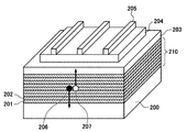
- FIG. 1 is a diagram for conceptually explaining the flow of photogenerated carriers (electrons and holes) in a solar cell having the superlattice structure described above.
- a superlattice structure 210 in which a plurality of crystalline Si layers 201 and SiO 2 layers 202 are alternately stacked is provided on the main surface of an n-type Si substrate 200.
- a p-type Si layer 203, a transparent conductive film layer 204, and a surface electrode 205 are sequentially formed on the upper surface.
- the thickness of the SiO 2 layer 202 is optimized to increase the thickness.
- dopant in this case, donor P, etc. in this case
- contact formation cannot be performed as designed.
- the present invention has been made in view of such problems, and the object of the present invention is to efficiently convert photogenerated carriers into currents to increase internal quantum efficiency, thereby increasing the photoelectric conversion efficiency. It is an object of the present invention to provide a solar cell, and to provide a solar cell capable of avoiding the problem of dopant diffusion inevitably caused by annealing at a high temperature and capable of performing contact formation as designed.
- a solar cell according to the present invention includes a structure portion having a superlattice structure in which a plurality of crystalline Si layers and SiO 2 layers are alternately stacked on a substrate having an insulating surface.
- the crystalline Si layer is substantially an intrinsic semiconductor layer
- the first side surface of the superlattice structure is a p-type superlattice in which a plurality of p-type crystalline Si layers and SiO 2 layers are alternately stacked.
- the second side surface opposite to the first side surface has an n-type superlattice structure in which a plurality of n-type crystalline Si layers and SiO 2 layers are alternately stacked, and the p-type The crystalline Si layer and the intrinsic crystalline Si layer are pi-junctioned, and the n-type crystalline Si layer and the intrinsic crystalline Si layer are ni-junctioned.
- a plurality of the superlattice structures are formed on the substrate so as to be separated from each other.
- adjacent superlattice structures of the plurality of superlattice structures are arranged such that the p-type superlattice structures face each other and the n-type superlattice structures face each other.
- adjacent superlattice structures of the plurality of superlattice structures are arranged such that the p-type superlattice structure and the n-type superlattice structure face each other.
- a p-type electrode or an n-type electrode is formed in a region where the superlattice structures are separated from each other.
- the superlattice structure has a mesa shape having an inclination on a side surface on which the p-type superlattice structure and the n-type superlattice structure are formed.
- the acceptor in the p-type crystalline Si layer and the donor in the n-type crystalline Si layer are ion-implanted impurities.
- the crystalline Si layer has a thickness of 5 nm or less.
- the substrate is a translucent substrate.
- the thickness of the SiO 2 layer constituting the superlattice structure is thicker toward the light receiving side.
- the distance between the first side surface and the second side surface of the superlattice structure is 10 ⁇ m or less.
- an opening is provided in a central region of the superlattice structure.
- the superlattice structure includes an electrode pattern in which a p-type electrode and an n-type electrode are formed in regions spaced from each other in series.
- the superlattice structure is provided with an electrode pattern in which a p-type electrode and an n-type electrode formed in regions separated from each other are connected in parallel.
- the solar cell of the present invention is a tandem solar cell in which a top cell provided on the light incident side and a bottom cell provided below the top cell are laminated, and the top cell includes the above-described structure.
- the bottom cell may be made of crystalline Si, and a light receiving surface electrode may be provided on the surface of the top cell, and a back electrode may be provided on the back surface of the bottom cell.
- junction pi junction and ni junction
- the problem of irreversible diffusion of dopants from the unintended substrate associated with annealing at a relatively high temperature to crystallize the Si layer is avoided. It is possible to perform contact formation almost as designed.
- FIG. 2 is a diagram for conceptually explaining the structure of a solar cell in which a plurality of adjacent superlattice structures are arranged such that p-type superlattice structures face each other and n-type superlattice structures face each other. is there.
- the superlattice structure has the mesa shape which has the inclination in the side surface in which the p-type superlattice structure and the n-type superlattice structure are formed. It is a figure for demonstrating the structural example by which the opening part is provided in the center area
- the crystalline Si layer may be a single crystal Si layer or a polycrystalline Si layer.
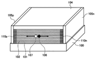
- FIG. 2 is a cross-sectional view for explaining the outline of the basic structure of the solar cell according to the present invention.
- a superlattice structure is formed by alternately laminating a plurality of crystalline Si layers 101 and SiO 2 layers 102 on the main surface of a substrate 100 having an insulating surface.
- the crystalline Si layer 101 is substantially an intrinsic semiconductor.
- the first side surface (left side surface in this figure) of the superlattice structure is a p-type superlattice structure 110p in which a plurality of p-type crystalline Si layers and SiO 2 layers are alternately stacked.
- the second side surface (right side surface in this figure) opposite to the first side surface is an n-type superlattice structure 110n in which a plurality of n-type crystalline Si layers and SiO 2 layers are alternately stacked. Then, the p-type crystalline Si layer constituting the p-type superlattice structure 110p and the intrinsic crystalline Si layer constituting the superlattice structure are pi-joined to form an n-type crystalline Si layer constituting the n-type superlattice structure 110n.
- the intrinsic crystalline Si layer constituting the superlattice structure is in ni junction.
- a p-type electrode 105p and an n-type electrode 105n are formed on each of the p-type superlattice structure 110p and the n-type superlattice structure 110n, and what is indicated by reference numeral 104 in the figure is a protective film.
- the solar cell according to the present invention includes a structural portion having a superlattice structure in which a plurality of crystalline Si layers and SiO 2 layers are alternately stacked on a substrate having an insulating surface, and the crystalline Si layer Is substantially an intrinsic semiconductor layer, and the first side surface of the superlattice structure has a p-type superlattice structure in which a plurality of p-type crystalline Si layers and SiO 2 layers are alternately stacked, and The second side surface opposite to the first side surface has an n-type superlattice structure in which a plurality of n-type crystalline Si layers and SiO 2 layers are alternately stacked, and the p-type crystalline Si layer and the The intrinsic crystalline Si layer has a pi junction, and the n-type crystalline Si layer and the intrinsic crystalline Si layer have a ni junction.
- the pi junction between the p-type crystalline Si layer constituting the p-type superlattice structure 110p and the intrinsic crystalline Si layer constituting the superlattice structure, and the n-type crystalline Si constituting the n-type superlattice structure 110n Each of the ni junctions of the intrinsic crystalline Si layer constituting the layer and the superlattice structure is formed on the side surface of the superlattice structure.
- the substrate 100 only needs to have an insulating surface, and may be, for example, a substrate in which an insulating film such as SiO 2 is provided on an n-type or p-type Si substrate, as well as an insulating substrate such as a quartz substrate.
- the substrate In the case of a solar cell having a structure in which the substrate side is a light incident surface, the substrate needs to be a translucent substrate.
- a texture layer made of a material such as ZnO is provided on the surface of the superlattice structure to increase the reflectance on the back surface (surface opposite to the substrate). You may do it.
- the p-type crystalline Si layer constituting the p-type superlattice structure 110p and the intrinsic crystalline Si layer constituting the superlattice structure are pi-junctioned to form an n-type superlattice structure.
- the n-type crystalline Si layer constituting 110n and the intrinsic crystalline Si layer constituting the superlattice structure are in ni junction. That is, this solar cell has a p-type superlattice / i-type superlattice / n-type superlattice structure, and the pi junction and the ni junction are composed of only a superlattice in which a plurality of Si layers / SiO 2 layers are stacked. ing.
- p-type and n-type polysilicon electrodes having no superlattice structure are formed on opposite sides of a superlattice structure in which a plurality of crystalline Si layers and SiO 2 layers are alternately stacked.
- the band gap of these junction regions is that of the polysilicon electrode (about 1.1 eV), and the open circuit voltage of the solar cell is regulated by this value, which may cause a decrease in the open circuit voltage in the junction region.
- Such a pi junction and ni junction are formed by, for example, ion-implanting a p-type impurity (acceptor) or an n-type impurity (donor) on the side surface after the superlattice structure is formed.
- the thickness of the crystalline Si layer constituting the superlattice structure In order to ensure the effect of increasing the open-circuit voltage by widening the band gap by the quantum size effect, it is preferable to design the thickness of the crystalline Si layer constituting the superlattice structure to 5 nm or less. Further, the refractive index of the superlattice structure can be changed by controlling the thickness of the SiO 2 layer constituting the superlattice structure. By utilizing this principle, it is possible to increase the photoelectric conversion efficiency by designing the SiO 2 layer constituting the superlattice structure to be thicker toward the light receiving side (light incident surface side).
- FIG. 2 shows only one superlattice structure as described above, but when configuring as a solar cell, it is of course possible to provide a plurality of such superlattice structures adjacent to each other. is there.
- FIG. 3 is a diagram for conceptually explaining the structure of a solar cell in which a plurality of the above-described superlattice structures 110 are formed on a substrate 100 whose surface is insulatively spaced from each other.
- adjacent superlattice structures are regions in which the p-type superlattice structure 110p and the n-type superlattice structure 110n are arranged to face each other and the superlattice structures are separated from each other.
- a p-type electrode or an n-type electrode is formed.
- a plurality of adjacent superlattice structures 110 are formed so that the p-type superlattice structures 110p face each other and the n-type superlattice It is good also as an aspect by which 110 n of structures are arrange
- the superlattice structure 110 may have a mesa shape having an inclined side surface on which the p-type superlattice structure 110p and the n-type superlattice structure 110n are formed. Good. In the case of such a mesa-shaped superlattice structure 110, it is easy to control the distribution of implanted ions when the p-type superlattice structure 110p and the n-type superlattice structure 110n are formed by ion implantation. There are advantages.
- a structure in which an opening 108 is provided in the central region of the superlattice structure may be employed.
- an opening 108 is provided, when a relatively large number of defects are included in the crystalline Si layer 101 constituting the superlattice structure, the defects are not removed by hydrogenation. There is an advantage that it becomes easy to activate.
- the distance between the first side surface (the surface on which the p-type superlattice structure 110p is formed) and the second side surface (the surface on which the n-type superlattice structure 110n is formed) is preferably 10 ⁇ m or less.
- the diameter of 108 is, for example, about 2 ⁇ m.
- Example of electrode pattern design In a solar cell having a structure in which a plurality of superlattice structures are provided adjacent to each other, a special method for interconnecting the p-type electrode and the n-type electrode provided in each structural part having the superlattice structure There is no limit.
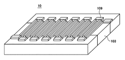
- the superlattice structure may be configured to include an electrode pattern 109 that connects the p-type electrode and the n-type electrode formed in a region separated from each other in parallel.
- a perspective view of the solar cell 10 in this case is shown in FIG. 8A.
- reference numeral 103 in the figure denotes a wall forming portion.
- the superlattice structure may be provided with an electrode pattern 109 in which a p-type electrode and an n-type electrode are connected in series, which are formed in regions separated from each other.
- a perspective view of the solar cell 10 in this case is shown in FIG. 8B.
- the solar cell having the above-described structure can be a tandem solar cell.
- FIG. 9 is a diagram for explaining an example in which the structure according to the present invention is applied to a tandem solar cell.
- Reference numeral 10 indicates a top cell
- reference numeral 20 indicates crystalline Si. Bottom cell.
- the structure shown in FIG. 5 is used as the top cell.
- substrate in this case needs to have translucency.
- this solar cell is a tandem solar cell in which a top cell provided on the light incident side and a bottom cell provided below the top cell are stacked, and the top cell includes the above-described structure,
- the bottom cell is made of crystalline Si, and a light receiving surface electrode is provided on the surface of the top cell 10, and a back electrode is provided on the back surface of the bottom cell 20.
- the solar cell according to the present invention it is not necessary to cross the high energy barrier of the SiO 2 layer when the photogenerated carriers diffuse in the superlattice structure composed of the crystalline Si layer / SiO 2 layer. Therefore, restrictions on the thickness of the SiO 2 layer are eased, loss of carriers during diffusion is remarkably suppressed, and a solar cell with high photoelectric conversion efficiency can be obtained by increasing the internal quantum efficiency.
Landscapes
- Photovoltaic Devices (AREA)
Abstract
本発明に係る太陽電池では、光生成したキャリアが結晶性Si層/SiO2層からなる超格子構造体中を拡散する際にSiO2層が有する高いエネルギー障壁を横切る必要がないため、SiO2層の厚みに対する制約が緩和されるとともに、拡散中のキャリアのロスが顕著に抑制され、内部量子効率を高めて高い光電変換効率の太陽電池を得ることが可能となる。また、接合(pi接合およびni接合)を横方向に形成するため、ドーパント不純物を含有する基板を用いる必要がなく、Si層を結晶化させるための比較的高温でのアニールに伴う意図しない基板からのドーパントの不可逆的な拡散の問題を回避することができるため、コンタクト形成は概ね設計どおりに行うことが可能である。
Description
本発明は、太陽電池技術に関し、より詳細には、量子サイズ効果を利用した光電変換効率の高いシリコン太陽電池の技術に関する。
近年の環境保全への社会的関心が高まるにつれ、化石燃料に代替するクリーンエネルギーの技術開発の重要性は益々高くなってきている。このような社会背景の下、太陽電池は、自然エネルギーを利用した電力用デバイスとして普及してきたが、太陽電池が主要なエネルギー供給源として利用されるようになるためには、更なるコスト低減と光電変換効率の向上が求められる。
これまで、太陽電池の構造として種々のものが提案されてきているが、例えば特許文献1(特開2014-27119号公報)には、光吸収層を、例えばシリコンから成る半導体層と、この半導体層よりバンドギャップの大きな材料(例えば酸化シリコン)からなる障壁層とを交互に積層した超格子構造とした態様のものが開示されている。
図1は、上述の超格子構造を備える太陽電池において、光生成したキャリア(電子および正孔)の流れを概念的に説明するための図である。この図に示した例では、n型のSi基板200の主面上に、結晶性のSi層201とSiO2層202が交互に複数積層された超格子構造体210が設けられており、その上面に、p型Si層203と透明導電膜層204と表面電極205が順次形成されている。この太陽電池に光が入射すると、超格子構造体210を構成するSi層201中で電子206と正孔207が生成し、電子206はn型Si基板200側へ、正孔207はp型Si層203側へと、SiO2層202を横切りながら縦方向に拡散することにより電流が流れることになる。
しかし、このような電流は、キャリアがSiO2層202が有する高いエネルギー障壁をトンネル効果により横切ること(透過する)で生じるものであるため、SiO2層202の厚みを最適化してその厚みを高い精度で制御することが必要になるだけでなく、拡散中のキャリアのロスを招き、内部量子効率を高めて高い光電変換効率の太陽電池を得るという観点からは望ましくない。加えて、Si層201を結晶化させるために行う比較的高温でのアニールに伴い、n型Si基板からドーパント(この場合はドナーであるPなど)が不可避的に拡散して、n側でのコンタクト形成が設計どおりに行えないという懸念もある。
本発明は、このような問題に鑑みてなされたものであって、その目的とするところは、光生成したキャリアを効率的に電流に変換して内部量子効率を高めることにより高い光電変換効率の太陽電池を提供すること、また、高温でのアニールに伴い不可避的に生じるドーパントの拡散の問題を回避し、コンタクト形成を設計どおりに行うことが可能な太陽電池を提供することにある。
上述の課題を解決するために、本発明に係る太陽電池は、表面が絶縁性の基板上に、結晶性Si層とSiO2層が交互に複数積層された超格子構造体を有する構造部を備え、前記結晶性Si層は実質的に真性半導体層であり、前記超格子構造体の第1の側面はp型の結晶性Si層とSiO2層が交互に複数積層されたp型超格子構造とされるとともに、前記第1の側面に対向する第2の側面はn型の結晶性Si層とSiO2層が交互に複数積層されたn型超格子構造とされており、前記p型の結晶性Si層と前記真性の結晶性Si層がpi接合するとともに、前記n型の結晶性Si層と前記真性の結晶性Si層がni接合している、ことを特徴とする。
ある態様では、前記基板上に、前記超格子構造体が相互に離間して複数形成されている。
また、ある態様では、前記複数の超格子構造体の隣接する超格子構造体は、前記p型超格子構造同士が対向するとともに、前記n型超格子構造同士が対向して配置されている。
また、ある態様では、前記複数の超格子構造体の隣接する超格子構造体は、前記p型超格子構造と前記n型超格子構造同士が対向して配置されている。
さらに、ある態様では、前記超格子構造体が相互に離間する領域に、p型電極もしくはn型電極が形成されている。
また、好ましい態様では、前記超格子構造体は、前記p型超格子構造および前記n型超格子構造が形成されている側面に傾斜を有するメサ形状を有している。
例えば、前記p型の結晶性Si層中のアクセプタおよび前記n型の結晶性Si層中のドナーは、イオン注入された不純物である。
好ましくは、前記結晶性Si層の厚みは5nm以下である。
また、好ましくは、前記基板は透光性基板である。
ある態様では、前記超格子構造体を構成するSiO2層の厚みは受光側ほど厚い。
また、ある態様では、前記超格子構造体の前記第1の側面と前記第2の側面との距離は10μm以下である。
さらに、ある態様では、前記超格子構造体の中央領域に開口部が設けられている。
ある態様では、前記超格子構造体が相互に離間する領域に形成されたp型電極およびn型電極を直列接続する電極パターンを備えている。
また、別の態様では、前記超格子構造体が相互に離間する領域に形成されたp型電極およびn型電極を並列接続する電極パターンを備えている。
本発明の太陽電池は、光入射側に設けられたトップセルと該トップセルの下方に設けられたボトムセルが積層されたタンデム型の太陽電池であって、前記トップセルは上述した構造部を備え、前記ボトムセルは結晶性Siからなり、前記トップセルの表面には受光面電極が、前記ボトムセルの裏面には裏面電極が設けられている態様とすることもできる。
本発明に係る太陽電池では、光生成したキャリアが結晶性Si層/SiO2層からなる超格子構造体中を拡散する際にSiO2層が有する高いエネルギー障壁を横切る必要がないため、SiO2層の厚みに対する制約が緩和されるとともに、拡散中のキャリアのロスが顕著に抑制され、内部量子効率を高めて高い光電変換効率の太陽電池を得ることが可能となる。
また、接合(pi接合およびni接合)を横方向に形成するため、Si層を結晶化させるための比較的高温でのアニールに伴う意図しない基板からのドーパントの不可逆的な拡散の問題を回避することができ、コンタクト形成を概ね設計どおりに行うことが可能である。
以下に、図面を参照して、本発明に係る太陽電池の構造について説明する。なお、以降の説明において、結晶性Si層は、単結晶Si層であっても多結晶Si層であってもよい。
[基本構造の概略]
図2は、本発明に係る太陽電池の基本構造の概略を説明するための断面図である。この図に示した例では、表面が絶縁性の基板100の主面上に、結晶性のSi層101とSiO2層102が交互に複数積層されて超格子構造体を形成している。なお、結晶性Si層101は実質的に真性半導体である。この超格子構造体の第1の側面(この図では左側面)はp型の結晶性Si層とSiO2層が交互に複数積層されたp型超格子構造110pとされている。また、第1の側面に対向する第2の側面(この図では右側面)はn型の結晶性Si層とSiO2層が交互に複数積層されたn型超格子構造110nとされている。そして、p型超格子構造110pを構成するp型結晶性Si層と超格子構造体を構成する真性結晶性Si層はpi接合し、n型超格子構造110nを構成するn型結晶性Si層と超格子構造体を構成する真性結晶性Si層はni接合している。なお、p型超格子構造110pとn型超格子構造110nのそれぞれには、p型電極105pとn型電極105nが形成されており、図中に符号104で示したものは保護膜である。
図2は、本発明に係る太陽電池の基本構造の概略を説明するための断面図である。この図に示した例では、表面が絶縁性の基板100の主面上に、結晶性のSi層101とSiO2層102が交互に複数積層されて超格子構造体を形成している。なお、結晶性Si層101は実質的に真性半導体である。この超格子構造体の第1の側面(この図では左側面)はp型の結晶性Si層とSiO2層が交互に複数積層されたp型超格子構造110pとされている。また、第1の側面に対向する第2の側面(この図では右側面)はn型の結晶性Si層とSiO2層が交互に複数積層されたn型超格子構造110nとされている。そして、p型超格子構造110pを構成するp型結晶性Si層と超格子構造体を構成する真性結晶性Si層はpi接合し、n型超格子構造110nを構成するn型結晶性Si層と超格子構造体を構成する真性結晶性Si層はni接合している。なお、p型超格子構造110pとn型超格子構造110nのそれぞれには、p型電極105pとn型電極105nが形成されており、図中に符号104で示したものは保護膜である。
すなわち、本発明に係る太陽電池は、表面が絶縁性の基板上に、結晶性Si層とSiO2層が交互に複数積層された超格子構造体を有する構造部を備え、前記結晶性Si層は実質的に真性半導体層であり、前記超格子構造体の第1の側面はp型の結晶性Si層とSiO2層が交互に複数積層されたp型超格子構造とされるとともに、前記第1の側面に対向する第2の側面はn型の結晶性Si層とSiO2層が交互に複数積層されたn型超格子構造とされており、前記p型の結晶性Si層と前記真性の結晶性Si層がpi接合するとともに、前記n型の結晶性Si層と前記真性の結晶性Si層がni接合している構造を有している。
この太陽電池に光が入射すると、超格子構造体を構成する真性結晶性Si層101中で電子106と正孔107が生成し、電子106はn型電極105n側へ、正孔107はp型電極105p側へと拡散することにより電流が流れることになる。つまり、この構成の太陽電池では、光生成したキャリアが結晶性Si層/SiO2層からなる超格子構造体中を拡散する際にSiO2層が有する高いエネルギー障壁を横切る必要がない。加えて、超格子構造体を構成するそれぞれの真性結晶性Si層101の面内では、電界の印加に関わらず、キャリアは局在することなく面内全体に広がる状態が維持される。このため、SiO2層の厚みに対する制約が緩和されるとともに、拡散中のキャリアのロスが顕著に抑制され、内部量子効率を高めて高い光電変換効率の太陽電池を得ることが可能となる。
しかも、p型超格子構造110pを構成するp型結晶性Si層と超格子構造体を構成する真性結晶性Si層のpi接合、および、n型超格子構造110nを構成するn型結晶性Si層と超格子構造体を構成する真性結晶性Si層のni接合は、何れも超格子構造体の側面に形成されている。従来構造のものでは、超格子と基板との間でpi接合もしくはni接合を形成するためにドーパント不純物を含有する基板を用いる必要があったが、本発明では斯かる基板を用いる必要がなくなる。その結果、スパッタリング等の手法で成膜されたSi層を結晶化させるための比較的高温(例えば1000~1100℃)でのアニールに伴う意図しない基板からのドーパントの不可逆的な拡散の問題を回避することができる。このため、本件発明の場合、コンタクト形成が概ね設計どおりに行うことが可能となる。
基板100はその表面が絶縁性であればよく、石英基板等の絶縁性基板はもとより、例えば、n型もしくはp型のSi基板上にSiO2等の絶縁膜を設けた基板などでもよい。なお、基板側を光入射面とする構造の太陽電池の場合には、基板は透光性基板である必要がある。また、基板側を光入射面とする構造の太陽電池の場合、超格子構造体の表面にZnO等の材料から成るテクスチャ層を設けて裏面(基板と反対側の面)での反射率を高めるようにしてもよい。
上述のとおり、本発明に係る太陽電池では、p型超格子構造110pを構成するp型結晶性Si層と超格子構造体を構成する真性結晶性Si層はpi接合し、n型超格子構造110nを構成するn型結晶性Si層と超格子構造体を構成する真性結晶性Si層はni接合している。つまり、この太陽電池は、p型超格子/i型超格子/n型超格子の構造を有し、pi接合とni接合はSi層/SiO2層が複数積層された超格子のみで構成されている。これは、pi接合領域とni接合領域に1.7eV程度の広いバンドギャップ(すなわち、超格子構造体のバンドギャップ)をもたせ、接合を形成したことに起因する開放電圧の低下を防ぐためである。
仮に、結晶性Si層とSiO2層が交互に複数積層された超格子構造体の対向する側面に、超格子構造を有さないp型およびn型のポリシリコン電極を形成してしまうと、これら接合領域のバンドギャップはポリシリコン電極のそれ(約1.1eV)となり、太陽電池の開放電圧はこの値に律則され、接合領域での開放電圧の低下を招く恐れがある。
このようなpi接合およびni接合は、例えば、上記超格子構造体を形成した後に、その側面にp型不純物(アクセプター)ないしn型不純物(ドナー)をイオン注入することで形成する。
量子サイズ効果によりバンドギャップを広げて開放電圧を高める効果を担保するためには、超格子構造体を構成する結晶性Si層の厚みを5nm以下に設計することが好ましい。また、超格子構造体を構成するSiO2層の厚みを制御すると超格子構造体の屈折率を変化させることができる。この原理を利用して、超格子構造体を構成するSiO2層の厚みが受光側(光入射面側)ほど厚くなるように設計し、光電変換効率を高めることも可能である。
[超格子構造体を複数有する構造の概略]
図2には、上述の超格子構造体がひとつのみ図示されているが、太陽電池として構成するに際しては、このような超格子構造体を隣接して複数設けるようにしてもよいことは勿論である。
図2には、上述の超格子構造体がひとつのみ図示されているが、太陽電池として構成するに際しては、このような超格子構造体を隣接して複数設けるようにしてもよいことは勿論である。
図3は、表面が絶縁性の基板100上に、上述した超格子構造体110が相互に離間して複数形成されている態様の太陽電池の構造を概念的に説明するための図である。
なお、この図に示した態様では、互いに隣接する超格子構造体は、p型超格子構造110pとn型超格子構造110n同士が対向して配置され、超格子構造体が相互に離間する領域に、p型電極もしくはn型電極が形成されているが、図4に示したように、隣接する複数の超格子構造体110が、p型超格子構造110p同士が対向するとともにn型超格子構造110n同士が対向して配置されている態様としてもよい。
また、図5に示したように、超格子構造体110は、p型超格子構造110pおよびn型超格子構造110nが形成されている側面に傾斜を有するメサ形状を有している態様としてもよい。このようなメサ形状の超格子構造体110とした場合には、p型超格子構造110pおよびn型超格子構造110nをイオン注入法により形成する際の注入イオンの分布制御が容易になる等の利点がある。
さらに、図6に示したように、超格子構造体の中央領域に開口部108が設けられている構造としてもよい。このような、開口部108を設けておくと、超格子構造体を構成する結晶性Si層101中に比較的多くの欠陥が含まれているような場合に、水素処理化により当該欠陥を不活性化し易くなるという利点がある。超格子構造体の第1の側面(p型超格子構造110p形成面)と第2の側面(n型超格子構造110n形成面)との距離は10μm以下であることが好ましいが、上記開口部108の直径は例えば2μm程度とする。
[電極パターンのデザイン例]
超格子構造体を隣接して複数設けた構成の太陽電池において、超格子構造体を有するそれぞれの構造部に設けられたp型電極およびn型電極をどのように相互接続するかについての特別な制限はない。
超格子構造体を隣接して複数設けた構成の太陽電池において、超格子構造体を有するそれぞれの構造部に設けられたp型電極およびn型電極をどのように相互接続するかについての特別な制限はない。
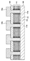
例えば図7Aに図示した一例のように、超格子構造体が相互に離間する領域に形成されたp型電極およびn型電極を並列接続する電極パターン109を備えている構成としてもよい。この場合の太陽電池10の斜視図を図8Aに示す。なお、図中の符号103はウォール形成部である。
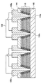
また、例えば図8Aに図示した一例のように、超格子構造体が相互に離間する領域に形成されたp型電極およびn型電極を直列接続する電極パターン109を備えている構成としてもよい。この場合の太陽電池10の斜視図を図8Bに示す。
[タンデム型太陽電池への応用]
上述した構造を有する太陽電池は、タンデム型の太陽電池とすることもできる。
上述した構造を有する太陽電池は、タンデム型の太陽電池とすることもできる。
図9は、本発明に係る構造体を、タンデム型太陽電池に応用した例を説明するための図で、符号10で示したものはトップセル、符号20で示したものは結晶性Siから成るボトムセルである。この図に示した例では、トップセルとして、図5に示した構造部を利用している。なお、この場合の基板は透光性を有するものであることが必要であることは言うまでもない。
すなわち、この太陽電池は、光入射側に設けられたトップセルと該トップセルの下方に設けられたボトムセルが積層されたタンデム型の太陽電池であって、トップセルは上述した構造部を備え、ボトムセルは結晶性Siからなり、トップセル10の表面には受光面電極が、ボトムセル20の裏面には裏面電極が設けられている。
このように、本発明に係る太陽電池では、光生成したキャリアが結晶性Si層/SiO2層からなる超格子構造体中を拡散する際にSiO2層が有する高いエネルギー障壁を横切る必要がないため、SiO2層の厚みに対する制約が緩和されるとともに、拡散中のキャリアのロスが顕著に抑制され、内部量子効率を高めて高い光電変換効率の太陽電池を得ることが可能となる。
100 基板
101 結晶性Si層
102 SiO2層
103 ウォール部
104 保護膜
105p p型電極
105n n型電極
106 電子
107 正孔
108 開口部
109 電極パターン
110p p型超格子構造
110n n型超格子構造
101 結晶性Si層
102 SiO2層
103 ウォール部
104 保護膜
105p p型電極
105n n型電極
106 電子
107 正孔
108 開口部
109 電極パターン
110p p型超格子構造
110n n型超格子構造
Claims (15)
- 表面が絶縁性の基板上に、結晶性Si層とSiO2層が交互に複数積層された超格子構造体を有する構造部を備え、
前記結晶性Si層は実質的に真性半導体層であり、
前記超格子構造体の第1の側面はp型の結晶性Si層とSiO2層が交互に複数積層されたp型超格子構造とされるとともに、前記第1の側面に対向する第2の側面はn型の結晶性Si層とSiO2層が交互に複数積層されたn型超格子構造とされており、
前記p型の結晶性Si層と前記真性の結晶性Si層がpi接合するとともに、前記n型の結晶性Si層と前記真性の結晶性Si層がni接合している、
ことを特徴とする太陽電池。 - 前記基板上に、前記超格子構造体が相互に離間して複数形成されている、請求項1に記載の太陽電池。
- 前記複数の超格子構造体の隣接する超格子構造体は、前記p型超格子構造同士が対向するとともに、前記n型超格子構造同士が対向して配置されている、請求項2に記載の太陽電池。
- 前記複数の超格子構造体の隣接する超格子構造体は、前記p型超格子構造と前記n型超格子構造同士が対向して配置されている、請求項2に記載の太陽電池。
- 前記超格子構造体が相互に離間する領域に、p型電極もしくはn型電極が形成されている、請求項2に記載の太陽電池。
- 前記超格子構造体は、前記p型超格子構造および前記n型超格子構造が形成されている側面に傾斜を有するメサ形状を有している、請求項1~5の何れか1項に記載の太陽電池。
- 前記p型の結晶性Si層中のアクセプタおよび前記n型の結晶性Si層中のドナーは、イオン注入された不純物である、請求項1~5の何れか1項に記載の太陽電池。
- 前記結晶性Si層の厚みは5nm以下である、請求項1~5の何れか1項に記載の太陽電池。
- 前記基板は透光性基板である、請求項1~5の何れか1項に記載の太陽電池。
- 前記超格子構造体を構成するSiO2層の厚みは受光側ほど厚い、請求項1~5の何れか1項に記載の太陽電池。
- 前記超格子構造体の前記第1の側面と前記第2の側面との距離は10μm以下である、請求項1~5の何れか1項に記載の太陽電池。
- 前記超格子構造体の中央領域に開口部が設けられている、請求項1~5の何れか1項に記載の太陽電池。
- 前記超格子構造体が相互に離間する領域に形成されたp型電極およびn型電極を直列接続する電極パターンを備えている、請求項5に記載の太陽電池。
- 前記超格子構造体が相互に離間する領域に形成されたp型電極およびn型電極を並列接続する電極パターンを備えている、請求項5に記載の太陽電池。
- 光入射側に設けられたトップセルと該トップセルの下方に設けられたボトムセルが積層されたタンデム型の太陽電池であって、
前記トップセルは請求項1~5の何れか1項に記載の構造部を備え、
前記ボトムセルは結晶性Siからなり、
前記トップセルの表面には受光面電極が、前記ボトムセルの裏面には裏面電極が設けられている、
ことを特徴とする太陽電池。
Applications Claiming Priority (2)
| Application Number | Priority Date | Filing Date | Title |
|---|---|---|---|
| JP2016052540A JP2019083220A (ja) | 2016-03-16 | 2016-03-16 | 太陽電池 |
| JP2016-052540 | 2016-03-16 |
Publications (1)
| Publication Number | Publication Date |
|---|---|
| WO2017159281A1 true WO2017159281A1 (ja) | 2017-09-21 |
Family
ID=59850312
Family Applications (1)
| Application Number | Title | Priority Date | Filing Date |
|---|---|---|---|
| PCT/JP2017/006995 Ceased WO2017159281A1 (ja) | 2016-03-16 | 2017-02-24 | 太陽電池 |
Country Status (2)
| Country | Link |
|---|---|
| JP (1) | JP2019083220A (ja) |
| WO (1) | WO2017159281A1 (ja) |
Families Citing this family (2)
| Publication number | Priority date | Publication date | Assignee | Title |
|---|---|---|---|---|
| USRE50352E1 (en) | 2013-05-09 | 2025-03-25 | Pronoia, Inc. | Quantum dipole battery |
| US20240250156A1 (en) * | 2023-01-23 | 2024-07-25 | Pronoia, Inc. | Quantum Dipole Battery |
Citations (6)
| Publication number | Priority date | Publication date | Assignee | Title |
|---|---|---|---|---|
| JPS6195576A (ja) * | 1984-10-17 | 1986-05-14 | Zenko Hirose | ヘテロ接合超格子構造を用いた高効率の高起電力光電池素子 |
| JPS6195575A (ja) * | 1984-10-17 | 1986-05-14 | Zenko Hirose | 超格子構造を用いた高起電力光電池素子 |
| US20100081228A1 (en) * | 2006-05-03 | 2010-04-01 | Rochester Institute Of Technology | Nanostructured quantum dots or dashes in photovoltaic devices and methods thereof |
| JP2010186915A (ja) * | 2009-02-13 | 2010-08-26 | Panasonic Corp | 太陽電池 |
| JP2012124392A (ja) * | 2010-12-10 | 2012-06-28 | Hitachi Ltd | 太陽電池の製造方法 |
| JP2012521660A (ja) * | 2009-03-23 | 2012-09-13 | 本田技研工業株式会社 | 原子層堆積法により製造された量子閉じ込め型太陽電池 |
-
2016
- 2016-03-16 JP JP2016052540A patent/JP2019083220A/ja active Pending
-
2017
- 2017-02-24 WO PCT/JP2017/006995 patent/WO2017159281A1/ja not_active Ceased
Patent Citations (6)
| Publication number | Priority date | Publication date | Assignee | Title |
|---|---|---|---|---|
| JPS6195576A (ja) * | 1984-10-17 | 1986-05-14 | Zenko Hirose | ヘテロ接合超格子構造を用いた高効率の高起電力光電池素子 |
| JPS6195575A (ja) * | 1984-10-17 | 1986-05-14 | Zenko Hirose | 超格子構造を用いた高起電力光電池素子 |
| US20100081228A1 (en) * | 2006-05-03 | 2010-04-01 | Rochester Institute Of Technology | Nanostructured quantum dots or dashes in photovoltaic devices and methods thereof |
| JP2010186915A (ja) * | 2009-02-13 | 2010-08-26 | Panasonic Corp | 太陽電池 |
| JP2012521660A (ja) * | 2009-03-23 | 2012-09-13 | 本田技研工業株式会社 | 原子層堆積法により製造された量子閉じ込め型太陽電池 |
| JP2012124392A (ja) * | 2010-12-10 | 2012-06-28 | Hitachi Ltd | 太陽電池の製造方法 |
Also Published As
| Publication number | Publication date |
|---|---|
| JP2019083220A (ja) | 2019-05-30 |
Similar Documents
| Publication | Publication Date | Title |
|---|---|---|
| CN101490851B (zh) | 具有减少的基极扩散面积的太阳能电池 | |
| JP6059173B2 (ja) | 太陽電池 | |
| CN104124302B (zh) | 太阳能电池和制造该太阳能电池的方法 | |
| JP2015130527A (ja) | 太陽電池及びその製造方法 | |
| KR20140135881A (ko) | 태양 전지 및 이의 제조 방법 | |
| JP2014072530A (ja) | 太陽電池及びその製造方法 | |
| JP7693939B2 (ja) | ペロブスカイト材料バイパスダイオード及びその製造方法、ペロブスカイト太陽電池モジュール及びその製造方法、太陽光発電モジュール | |
| JP5708695B2 (ja) | 太陽電池セル | |
| KR102053140B1 (ko) | 태양 전지 | |
| JP2006173381A (ja) | 光起電力素子 | |
| JP6188921B2 (ja) | 太陽電池および太陽電池の製造方法 | |
| US10141467B2 (en) | Solar cell and method for manufacturing the same | |
| KR20160052271A (ko) | 태양 전지 | |
| WO2015098426A1 (ja) | 太陽電池及びその製造方法 | |
| KR101045859B1 (ko) | 태양 전지 및 그 제조 방법 | |
| JP5868661B2 (ja) | バイパスダイオードおよびその製造方法 | |
| JP2019083220A (ja) | 太陽電池 | |
| CN118825101A (zh) | 一种太阳能电池、电池组件及光伏系统 | |
| KR101757877B1 (ko) | 태양 전지 및 그의 제조 방법 | |
| KR101680384B1 (ko) | 태양 전지의 제조 방법 | |
| US20140251422A1 (en) | Solar cell with doping blocks | |
| KR101630061B1 (ko) | 태양 전지 | |
| JP2023033940A (ja) | 太陽電池セルおよび太陽電池 | |
| KR20160061947A (ko) | 태양 전지 및 이의 제조 방법 | |
| CN223463285U (zh) | 一种太阳能电池、电池组件及光伏系统 |
Legal Events
| Date | Code | Title | Description |
|---|---|---|---|
| NENP | Non-entry into the national phase |
Ref country code: DE |
|
| 121 | Ep: the epo has been informed by wipo that ep was designated in this application |
Ref document number: 17766286 Country of ref document: EP Kind code of ref document: A1 |
|
| 122 | Ep: pct application non-entry in european phase |
Ref document number: 17766286 Country of ref document: EP Kind code of ref document: A1 |
|
| NENP | Non-entry into the national phase |
Ref country code: JP |