WO2017158979A1 - 処理装置およびコリメータ - Google Patents
処理装置およびコリメータ Download PDFInfo
- Publication number
- WO2017158979A1 WO2017158979A1 PCT/JP2016/087823 JP2016087823W WO2017158979A1 WO 2017158979 A1 WO2017158979 A1 WO 2017158979A1 JP 2016087823 W JP2016087823 W JP 2016087823W WO 2017158979 A1 WO2017158979 A1 WO 2017158979A1
- Authority
- WO
- WIPO (PCT)
- Prior art keywords
- collimator
- magnetic field
- processing apparatus
- hole
- component
- Prior art date
- Legal status (The legal status is an assumption and is not a legal conclusion. Google has not performed a legal analysis and makes no representation as to the accuracy of the status listed.)
- Ceased
Links
Images


Classifications
-
- C—CHEMISTRY; METALLURGY
- C23—COATING METALLIC MATERIAL; COATING MATERIAL WITH METALLIC MATERIAL; CHEMICAL SURFACE TREATMENT; DIFFUSION TREATMENT OF METALLIC MATERIAL; COATING BY VACUUM EVAPORATION, BY SPUTTERING, BY ION IMPLANTATION OR BY CHEMICAL VAPOUR DEPOSITION, IN GENERAL; INHIBITING CORROSION OF METALLIC MATERIAL OR INCRUSTATION IN GENERAL
- C23C—COATING METALLIC MATERIAL; COATING MATERIAL WITH METALLIC MATERIAL; SURFACE TREATMENT OF METALLIC MATERIAL BY DIFFUSION INTO THE SURFACE, BY CHEMICAL CONVERSION OR SUBSTITUTION; COATING BY VACUUM EVAPORATION, BY SPUTTERING, BY ION IMPLANTATION OR BY CHEMICAL VAPOUR DEPOSITION, IN GENERAL
- C23C14/00—Coating by vacuum evaporation, by sputtering or by ion implantation of the coating forming material
- C23C14/22—Coating by vacuum evaporation, by sputtering or by ion implantation of the coating forming material characterised by the process of coating
- C23C14/34—Sputtering
- C23C14/35—Sputtering by application of a magnetic field, e.g. magnetron sputtering
-
- C—CHEMISTRY; METALLURGY
- C23—COATING METALLIC MATERIAL; COATING MATERIAL WITH METALLIC MATERIAL; CHEMICAL SURFACE TREATMENT; DIFFUSION TREATMENT OF METALLIC MATERIAL; COATING BY VACUUM EVAPORATION, BY SPUTTERING, BY ION IMPLANTATION OR BY CHEMICAL VAPOUR DEPOSITION, IN GENERAL; INHIBITING CORROSION OF METALLIC MATERIAL OR INCRUSTATION IN GENERAL
- C23C—COATING METALLIC MATERIAL; COATING MATERIAL WITH METALLIC MATERIAL; SURFACE TREATMENT OF METALLIC MATERIAL BY DIFFUSION INTO THE SURFACE, BY CHEMICAL CONVERSION OR SUBSTITUTION; COATING BY VACUUM EVAPORATION, BY SPUTTERING, BY ION IMPLANTATION OR BY CHEMICAL VAPOUR DEPOSITION, IN GENERAL
- C23C14/00—Coating by vacuum evaporation, by sputtering or by ion implantation of the coating forming material
- C23C14/22—Coating by vacuum evaporation, by sputtering or by ion implantation of the coating forming material characterised by the process of coating
- C23C14/34—Sputtering
- C23C14/35—Sputtering by application of a magnetic field, e.g. magnetron sputtering
- C23C14/351—Sputtering by application of a magnetic field, e.g. magnetron sputtering using a magnetic field in close vicinity to the substrate
-
- C—CHEMISTRY; METALLURGY
- C23—COATING METALLIC MATERIAL; COATING MATERIAL WITH METALLIC MATERIAL; CHEMICAL SURFACE TREATMENT; DIFFUSION TREATMENT OF METALLIC MATERIAL; COATING BY VACUUM EVAPORATION, BY SPUTTERING, BY ION IMPLANTATION OR BY CHEMICAL VAPOUR DEPOSITION, IN GENERAL; INHIBITING CORROSION OF METALLIC MATERIAL OR INCRUSTATION IN GENERAL
- C23C—COATING METALLIC MATERIAL; COATING MATERIAL WITH METALLIC MATERIAL; SURFACE TREATMENT OF METALLIC MATERIAL BY DIFFUSION INTO THE SURFACE, BY CHEMICAL CONVERSION OR SUBSTITUTION; COATING BY VACUUM EVAPORATION, BY SPUTTERING, BY ION IMPLANTATION OR BY CHEMICAL VAPOUR DEPOSITION, IN GENERAL
- C23C14/00—Coating by vacuum evaporation, by sputtering or by ion implantation of the coating forming material
- C23C14/22—Coating by vacuum evaporation, by sputtering or by ion implantation of the coating forming material characterised by the process of coating
- C23C14/50—Substrate holders
-
- C—CHEMISTRY; METALLURGY
- C23—COATING METALLIC MATERIAL; COATING MATERIAL WITH METALLIC MATERIAL; CHEMICAL SURFACE TREATMENT; DIFFUSION TREATMENT OF METALLIC MATERIAL; COATING BY VACUUM EVAPORATION, BY SPUTTERING, BY ION IMPLANTATION OR BY CHEMICAL VAPOUR DEPOSITION, IN GENERAL; INHIBITING CORROSION OF METALLIC MATERIAL OR INCRUSTATION IN GENERAL
- C23C—COATING METALLIC MATERIAL; COATING MATERIAL WITH METALLIC MATERIAL; SURFACE TREATMENT OF METALLIC MATERIAL BY DIFFUSION INTO THE SURFACE, BY CHEMICAL CONVERSION OR SUBSTITUTION; COATING BY VACUUM EVAPORATION, BY SPUTTERING, BY ION IMPLANTATION OR BY CHEMICAL VAPOUR DEPOSITION, IN GENERAL
- C23C14/00—Coating by vacuum evaporation, by sputtering or by ion implantation of the coating forming material
- C23C14/22—Coating by vacuum evaporation, by sputtering or by ion implantation of the coating forming material characterised by the process of coating
- C23C14/50—Substrate holders
- C23C14/505—Substrate holders for rotation of the substrates
-
- H—ELECTRICITY
- H01—ELECTRIC ELEMENTS
- H01J—ELECTRIC DISCHARGE TUBES OR DISCHARGE LAMPS
- H01J37/00—Discharge tubes with provision for introducing objects or material to be exposed to the discharge, e.g. for the purpose of examination or processing thereof
- H01J37/32—Gas-filled discharge tubes
- H01J37/34—Gas-filled discharge tubes operating with cathodic sputtering
- H01J37/3402—Gas-filled discharge tubes operating with cathodic sputtering using supplementary magnetic fields
- H01J37/3405—Magnetron sputtering
-
- H—ELECTRICITY
- H01—ELECTRIC ELEMENTS
- H01J—ELECTRIC DISCHARGE TUBES OR DISCHARGE LAMPS
- H01J37/00—Discharge tubes with provision for introducing objects or material to be exposed to the discharge, e.g. for the purpose of examination or processing thereof
- H01J37/32—Gas-filled discharge tubes
- H01J37/34—Gas-filled discharge tubes operating with cathodic sputtering
- H01J37/3411—Constructional aspects of the reactor
- H01J37/3447—Collimators, shutters, apertures
-
- H—ELECTRICITY
- H01—ELECTRIC ELEMENTS
- H01J—ELECTRIC DISCHARGE TUBES OR DISCHARGE LAMPS
- H01J37/00—Discharge tubes with provision for introducing objects or material to be exposed to the discharge, e.g. for the purpose of examination or processing thereof
- H01J37/32—Gas-filled discharge tubes
- H01J37/34—Gas-filled discharge tubes operating with cathodic sputtering
- H01J37/3464—Operating strategies
- H01J37/347—Thickness uniformity of coated layers or desired profile of target erosion
-
- H—ELECTRICITY
- H10—SEMICONDUCTOR DEVICES; ELECTRIC SOLID-STATE DEVICES NOT OTHERWISE PROVIDED FOR
- H10P—GENERIC PROCESSES OR APPARATUS FOR THE MANUFACTURE OR TREATMENT OF DEVICES COVERED BY CLASS H10
- H10P14/00—Formation of materials, e.g. in the shape of layers or pillars
- H10P14/40—Formation of materials, e.g. in the shape of layers or pillars of conductive or resistive materials
- H10P14/42—Formation of materials, e.g. in the shape of layers or pillars of conductive or resistive materials using a gas or vapour
-
- H—ELECTRICITY
- H01—ELECTRIC ELEMENTS
- H01J—ELECTRIC DISCHARGE TUBES OR DISCHARGE LAMPS
- H01J2237/00—Discharge tubes exposing object to beam, e.g. for analysis treatment, etching, imaging
- H01J2237/32—Processing objects by plasma generation
- H01J2237/33—Processing objects by plasma generation characterised by the type of processing
- H01J2237/332—Coating
- H01J2237/3322—Problems associated with coating
- H01J2237/3323—Problems associated with coating uniformity
Definitions
- Embodiment relates to a processing apparatus and a collimator.
- a processing apparatus such as a sputtering apparatus provided with a collimator is known.
- the processing apparatus includes a container, a workpiece placement unit, a collimator, and a magnetic field generation unit.
- the processing object placement unit is provided in the container, and a processing object on which particles are stacked may be placed.
- the collimator is provided in the container, has a first surface and a second surface opposite to the first surface, and is provided with a through-hole penetrating the first surface and the second surface.
- the magnetic field generator is provided in the container and generates a magnetic field between the first surface and the second surface in the through hole.
- FIG. 1 is a schematic and exemplary cross-sectional view of a processing apparatus according to an embodiment.
- FIG. 2 is a schematic and exemplary cross-sectional view of a part including the through hole of the collimator of the first embodiment.
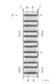
- FIG. 3 is a schematic and exemplary explanatory view including a plan view of the collimator according to the first embodiment and a partial enlarged view thereof.
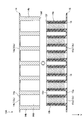
- FIG. 4 is a schematic and exemplary cross-sectional view of the collimator of the second embodiment.
- FIG. 5 is a schematic and exemplary exploded cross-sectional view of the collimator of the second embodiment.
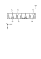
- FIG. 6 is a schematic and cross-sectional view of a modified collimator.
- a V direction (first direction) and an H direction (second direction) are defined.
- the V direction is the vertical direction
- the H direction is the horizontal direction.
- the V direction and the H direction are orthogonal to each other.
- FIG. 1 is a cross-sectional view of the sputtering apparatus 1.
- the sputtering apparatus 1 forms (stacks) a film of metal particles P on the surface of the wafer W, for example.
- the sputtering apparatus 1 is an example of a processing apparatus and can be referred to as a film forming apparatus or a stacking apparatus.
- the wafer W is an example of an object to be processed and can be referred to as an object.
- the sputtering apparatus 1 has a chamber 11.
- the chamber 11 is configured in a substantially cylindrical shape centering on a central axis along the V direction, and has a top wall 11a, a bottom wall 11b, and a peripheral wall 11c (side wall).
- the top wall 11a and the bottom wall 11b are orthogonal to the V direction and extend along the H direction.
- the bus bar of the peripheral wall 11c is along the V direction.
- the chamber 11 forms a processing chamber R as a substantially cylindrical space.
- the sputtering apparatus 1 is installed such that the central axis (V direction) of the chamber 11 is along the vertical direction.
- the chamber 11 is an example of a container.
- a target T can be disposed along the top wall 11a.
- the target T is supported by the top wall 11a via a backing plate, for example.
- the target T generates metal particles P.
- the target T can be referred to as a particle emission source or a particle generation source.
- the top wall 11a or the backing plate may be referred to as a discharge source arrangement part.
- a magnet M can be disposed outside the processing chamber R of the sputtering apparatus 1 along the top wall 11a.
- the target T generates metal particles P from a region close to the magnet M.
- a stage 12 is provided at a position close to the bottom wall 11b.
- the stage 12 supports the wafer W.
- the stage 12 has a plate 12a, a shaft 12b, and a support portion 12c.
- the plate 12a is configured in a disk shape, for example, and has a surface 12d orthogonal to the V direction.
- the plate 12a supports the wafer W on the surface 12d so that the surface wa of the wafer W is along a surface orthogonal to the V direction.
- the shaft 12b protrudes from the support portion 12c in the direction opposite to the V direction, and is connected to the plate 12a.
- the plate 12a is supported by the support portion 12c via the shaft 12b.
- the support portion 12c can change the position of the shaft 12b in the V direction.
- the support portion 12c may have a mechanism that can change the fixing position (holding position) of the shaft 12b, or a motor that can electrically change the position in the V direction of the shaft 12b. And an actuator including a rotation / linear motion conversion mechanism and the like.
- an actuator including a rotation / linear motion conversion mechanism and the like.
- the positions of the shaft 12b and the plate 12a can be set in multiple stages or continuously (continuously variable).
- the stage 12 (plate 12a) is an example of the workpiece placement unit.
- the stage 12 can be referred to as a workpiece support unit, a position change unit, and a position adjustment unit.
- a collimator 13 is disposed between the top wall 11a and the stage 12.
- the collimator 13 is supported by the peripheral wall 11 c of the chamber 11.
- the collimator 13 is configured in a substantially disc shape, and has a surface 13a and a surface 13b opposite to the surface 13a.
- the surfaces 13a and 13b are orthogonal to the V direction and extend in a planar shape along the H direction.
- the thickness direction of the collimator 13 is the V direction.
- the collimator 13 is provided with a plurality of through holes 13c penetrating the surface 13a and the surface 13b.
- the through hole 13c is opened to the target T side, that is, the top wall 11a side, and is opened to the wafer W side, that is, the stage 12 side.
- the through-hole 13c has, for example, a circular cross section and extends along the V direction. That is, the through hole 13c is formed in a cylindrical shape (cylindrical surface shape).
- the cross-sectional shape of the through hole 13c is not limited to a circle, and may be a polygonal shape such as a regular hexagon. Further, the through holes 13c may be arranged substantially equally at the same interval in the surface 13a (or in the surface 13b), and the arrangement interval and size (cross-sectional area, etc.) of the through holes 13c are determined by the location of the surface 13a. It may be different depending on.
- the particles P are rectified in the V direction by passing through the through holes 13c extending along the V direction. Therefore, the collimator 13 is referred to as a rectifying device or a rectifying member.
- the side surface 13d constituting the through hole 13c can be referred to as a rectifying unit.
- the side surface 13d can also be referred to as a circumferential surface or an inner surface.
- the surface 13a is an example of a first surface
- the surface 13b is an example of a second surface.
- the peripheral wall 11c of the chamber 11 is provided with a discharge port 11d.
- a pipe (not shown) extending from the discharge port 11d is connected to, for example, a suction pump (vacuum pump, not shown).
- a suction pump vacuum pump, not shown.
- the inlet 11e is provided in the peripheral wall 11c of the chamber 11, for example.
- a pipe (not shown) extending from the introduction port 11e is connected to, for example, a tank (not shown).
- the tank contains an inert gas such as argon gas. The inert gas in the tank can be introduced into the processing chamber R.
- a transparent window 11f is provided on the peripheral wall 11c of the chamber 11, for example.
- the collimator 13 can be photographed through the window 11f by the camera 20 disposed outside the chamber 11. From the image taken by the camera 20, the state of the collimator 13 can be confirmed by image processing.
- the transparent window 11f may be covered with a detachable or openable lid, a cover, a door, or the like.
- the peripheral wall 11c may be provided with an opening (through hole) instead of the transparent window 11f, and may be provided with a lid capable of opening and closing the opening.
- the lid, cover, door, etc. for example, can cover the window 11f or opening during the operation of the sputtering apparatus 1, and can open the window 11f or opening while the sputtering apparatus 1 is not operating.
- the argon gas introduced into the processing chamber R is ionized and plasma is generated.
- the argon ions collide with the target T for example, particles P of the metal material (film forming material) constituting the target T jump out from the lower surface ta of the target T. In this way, the target T releases the particles P.
- the direction in which the particles P fly from the lower surface ta of the target T is distributed according to the cosine law (Lambert's cosine law). That is, the particles P flying from a certain point on the lower surface ta of the target T fly most in the normal direction (vertical direction, V direction) of the lower surface ta. Therefore, the normal direction is an example of a direction in which the target T arranged on the top wall 11a or the backing plate (emission source arrangement unit) emits at least one particle.
- the number of particles flying in the direction inclined at an angle ⁇ with respect to the normal direction (crossing obliquely) is approximately proportional to the cosine (cos ⁇ ) of the number of particles flying in the normal direction.
- the particle P is a fine particle of the metal material of the target T.
- the particle P may be a particle of a substance such as a molecule, an atom, an atomic nucleus, an elementary particle, or a vapor (vaporized substance).
- the particles P may contain cations P1 such as copper ions having a positive charge.
- the collimator 13 is magnetized in order to deflect the positive ions P1 having such positive charges in the V direction.
- the collimator 13 is magnetized so that the wafer W side, that is, the surface 13b side becomes the N pole, and the target T side, that is, the surface 13a side, becomes the S pole.
- the collimator 13 is an example of a magnetized magnetic body and an example of a magnetic field generator.
- the collimator 13 may be magnetized as a whole, or a part of the collimator 13, for example, the peripheral portion of the through hole 13 c may be partially magnetized.
- FIG. 2 is a partial cross-sectional view including the through hole 13 c of the collimator 13. As shown in FIG. 2, the magnetized collimator 13 forms a magnetic field B from the surface 13b toward the surface 13a in the through hole 13c.
- FIG. 3 is an explanatory view including a plan view of the collimator 13 and a partially enlarged view thereof.
- the cation P1 receives the Lorentz force F by the magnetic field B formed in the through hole 13c, and turns in the V direction while spirally turning in the through hole 13c. Moving. At that time, the turning radius of the cation P1 decreases as it moves in the V direction.
- the amount of displacement of the cation P1 in the H direction is a value corresponding to the H direction component of the velocity vector when entering the through hole 13c of the cation P1, but the cation P1 entering the through hole 13c It is deflected toward the focal point by the magnetic field B formed in 13c and converges.
- the through hole 13c and the magnetic field B formed around it function as a magnetic lens for the positive ions P1.
- the distance L can be adjusted or set by changing the position of the shaft 12b with respect to the support portion 12c of the stage 12, for example.
- the focal point may be set at a predetermined position of the wafer W, such as the surface wa of the wafer W, or the focal point may be slightly above or below the V direction, that is, above or below in FIG. It may be set by shifting (offset).
- offset compared with the case where the focal point of the magnetic lens of the through hole 13c is set on the surface wa of the wafer W, the arrival of the positive ions P1 corresponding to each of the through holes 13c on the surface wa of the wafer W, for example.
- the range expands. Therefore, there may be a case where variations in film thickness depending on the location of the wafer W can be further reduced.
- deposits of particles P may be deposited on the surface 13a and the side surface 13d of the collimator 13. This narrows the region through which the cation P1 can pass in the through hole 13c, so that the focus of the cation P1 may change with time. Further, even when the surface 13a and the side surface 13d are eroded due to the influence of plasma or the like, the focus of the cation P1 can change over time.
- the state of the collimator 13 can be confirmed by an image taken by the camera 20 through the window 11f or the opening or by visual observation. Therefore, it is possible to change the distance L in accordance with the state of the collimator 13 and further reduce variations in film thickness depending on the location of the wafer W.
- the collimator 13 is magnetized so that the magnetic field B from the surface 13b (second surface) side to the surface 13a (first surface) side is generated in the through hole 13c of the collimator 13. ing. Therefore, when the cation P1 passes through the through-hole 13c while turning spirally in the through-hole 13c, the turning radius becomes small, so that the cation P1 converges at a position away from the through-hole 13c in the V direction. To do. Therefore, for example, in addition to the original rectifying effect of the collimator 13 with respect to the particles P, the magnetic convergence effect with respect to positively charged particles such as the positive ions P1 can be obtained, so that variations in film thickness depending on the location of the wafer W are easily reduced. .
- the magnetic field B may be a magnetic field from the surface 13a (first surface) side to the surface 13b (second surface) side. In this case, the same actions and effects as those described above can be obtained for the anions.
- the collimator 13 is a magnetic body, that is, a magnetic field generation unit. Therefore, for example, a configuration capable of obtaining a magnetic focusing effect on the cation P1 can be configured relatively simply.
- the distance between the collimator 13 and the plate 12a (processing object placement portion) of the stage 12 for example, the distance L between the surface 13b of the collimator 13 and the surface 12d of the plate 12a can be changed. Therefore, for example, variations in film thickness depending on the location of the wafer W can be suppressed.
- the collimator 13A of the present embodiment has a configuration similar to that of the collimator 13 of the first embodiment. Therefore, also by this embodiment, the same effect
- the present embodiment is different from the first embodiment in that the collimator 13A has an electromagnet.
- the collimator 13A can be installed instead of the collimator 13 in the chamber 11 of the first embodiment, for example.
- FIG. 4 is a cross-sectional view of the collimator 13A of the present embodiment.
- the collimator 13A includes a plurality of coils 16 wound around each of the plurality of through holes 13c.
- the coil 16 is constituted by, for example, a winding wound with a copper wire or the like.
- the coil 16 may have a coil bobbin.
- the coil 16 can function as an electromagnet when a current is passed through a wiring or the like (not shown) provided in the collimator 13A. Therefore, also in this embodiment, the magnetic field which goes to the surface 13a side from the surface 13b side can be formed in the through-hole 13c. Further, according to the present embodiment, the strength of the magnetic field can be changed by changing the value of the current flowing through the coil 16. As the strength of the magnetic field changes, the distance to the focal point changes. Therefore, according to the present embodiment, for example, by changing the magnitude (current value) of the current flowing through the coil 16, the strength of the magnetic field generated in the through hole 13c is changed. It is possible to reduce the variation in film thickness due to the above.
- the direction of the magnetic field generated in the coil 16 is changed by changing the direction of the current flowing through the coil 16, whereby the ions that are the targets of the above-described actions and effects of the magnetic field are either positive ions or negative ions. It can be switched between ions.
- the coil 16 is an example of a magnetic field generator.
- FIG. 5 is an exploded sectional view of the collimator 13A.
- the collimator 13 ⁇ / b> A is configured by integrating a first component 14 (first member) and a second component 15 (second member).
- the first component 14 located on the target T side is configured by ceramics having a relatively high resistance to plasma.
- the second component 15 including (supporting) the coil 16 and the wiring (not shown) is made of a synthetic resin material (plastic or engineering plastic) having high moldability.
- the coil 16 and the wiring can be relatively easily incorporated into the second component 15 by insert molding or the like.
- the coil 16 is insert-molded, for example, housed in a recess provided in the second part 15, attached to a rod-like part provided in the second part 15, or bonded to the second part 15. It may be incorporated into the second component 15 by other than the above.
- the collimator 13A may be configured so that the first component 14 and the second component 15 can be disassembled.
- the connection between the first component 14 and the second component 15 can take various forms such as press-fitting, snap-fit, and connection via a coupler or component (not shown).
- the second part 15 is removed from the collimator 13A (first part). 14) and can be replaced with a new second part 15. That is, in the collimator 13A, the second part 15 is a replacement part (consumable part).
- the entire collimator 13A is a replacement part (consumable)
- waste of materials and manufacturing and maintenance costs are likely to be reduced.
- the strength of the magnetic field and thus the distance to the convergence position by the through-hole 13c Since the (focal length) can be changed, it is possible to reduce variations in film thickness depending on the location on the wafer W. Further, for example, it is possible to change the specifications such as the length and size of the through hole 13c.
- the first part 14 may be a replacement part.
- a plurality of first parts 14 having different dimensions, materials, and the like can be prepared, and the first parts 14 incorporated in the collimator 13A can be changed. Thereby, for example, specifications such as the length and size of the through hole 13c can be changed.
- the first component 14 of the collimator 13 ⁇ / b> A includes a disk-shaped top wall portion 14 a and a columnar body 14 b extending from the top wall portion 14 a in the V direction.
- the surface 14f of the body 14b is provided with a cylindrical recess 14d that is open in the V direction.
- the top wall portion 14a is provided with a through hole 14c penetrating between the surface 14e and the concave portion 14d.
- the through hole 14c is a part of the through hole 13c.
- the body 14b is also a protruding portion protruding in the V direction from the top wall portion 14a.
- the surface 14e of the top wall portion 14a is the surface 13a of the collimator 13A.
- the second component 15 of the collimator 13A has a disk-like bottom wall portion 15a and a plurality of projecting portions 15b extending from the bottom wall portion 15a in the opposite direction to the V direction.
- the protruding portion 15 b is accommodated in the recess 14 d provided in the first component 14.
- the protruding portion 15b is provided with a through hole 15c continuous with the same diameter as the through hole 14c provided in the top wall portion 14a in a state where the first component 14 and the second component 15 are integrated.
- the through hole 15c is a part of the through hole 13c of the second component 15 of the collimator 13A.
- the body 14b of the first component 14 is accommodated in the gap 15d provided between the plurality of protruding portions 15b.
- a surface 15e of the bottom wall portion 15a is a surface 13b of the collimator 13A.
- the top wall portion 14a and the body 14b of the first component 14 cover the plurality of protruding portions 15b of the second component 15 from the target T side. That is, the first component 14 suppresses the second component 15 from being eroded by the plasma.
- the first component 14 can be referred to as a cover or a protective member.
- the collimator 13A includes the coil 16 wound around the through hole 13c. Therefore, for example, the strength of the magnetic field and the distance to the convergence position (focal length) by the through hole 13c can be changed depending on the magnitude (current value) of the current flowing through the coil 16, and therefore, depending on the location on the wafer W. Variations in film thickness can be reduced. In addition, for example, by changing the direction of the current flowing through the coil 16, the direction of the magnetic field is changed, and whether the ions to be subjected to the above-described actions and effects by the magnetic field are positive ions or negative ions, Can be switched.
- the collimator 13A is configured by integrating the first component 14 and the second component 15. Therefore, since the functions can be divided between the first component 14 and the second component 15, two features that are trade-offs are easily achieved.
- the first component 14 is a component having higher plasma resistance than the second component 15, for example, ceramic
- the second component 15 is a component in which the coil 16 can be easily incorporated, for example, a synthetic resin material
- the plasma resistance and manufacturability Are easier to achieve at a higher level.
- the second component 15 may support a magnetic material such as a permanent magnet instead of the coil 16.
- the collimator 13A is configured so that the second part 15 or the first part 14 can be replaced (detachable). Therefore, for example, compared to a case where the entire collimator 13A is replaced, waste of materials and manufacturing and maintenance costs are likely to be reduced.
- the first component 14 has higher plasma resistance than the second component 15 and covers the second component 15 from the opposite side of the stage 12 (processing object placement portion), that is, from the target T side or the top wall 11a side. ing.
- the first component 14 suppresses the second component 15 from being eroded by the plasma.
- the collimator 13B of this modification has the same configuration as the collimator 13 of the first embodiment. Therefore, also by this modification, the same effect
- the collimator 13B can be installed in place of the collimator 13 in the chamber 11 of the first embodiment, for example.
- FIG. 6 is a cross-sectional view of the collimator 13B of this modification.
- the cross-sectional area of the cross section perpendicular to the V direction of the through hole 13c is gradually reduced from the surface 13a toward the surface 13b.
- grains P in the said surface 13a tends to reduce.
- Such an inclination of the through-hole 13c can be applied to the split type collimator 13A and other collimators as in the second embodiment.
- the said embodiment is an example and is not intending limiting the range of invention.
- the embodiment can be implemented in various other forms, and various omissions, replacements, combinations, and changes can be made without departing from the scope of the invention.
- the embodiments are included in the scope and gist of the invention, and are included in the invention described in the claims and the equivalents thereof.
- the configuration and shape of the embodiment can be partially exchanged.
- the specifications (structure, type, direction, shape, size, length, width, thickness, height, angle, number, arrangement, position, material, etc.) of each configuration, shape, etc. are changed as appropriate.
- the processing apparatus may be an apparatus other than a sputtering apparatus such as a CVD apparatus.
Landscapes
- Chemical & Material Sciences (AREA)
- Engineering & Computer Science (AREA)
- Physics & Mathematics (AREA)
- Analytical Chemistry (AREA)
- Plasma & Fusion (AREA)
- Materials Engineering (AREA)
- Organic Chemistry (AREA)
- Metallurgy (AREA)
- Mechanical Engineering (AREA)
- Chemical Kinetics & Catalysis (AREA)
- Physical Vapour Deposition (AREA)
- Electrodes Of Semiconductors (AREA)
- Physical Deposition Of Substances That Are Components Of Semiconductor Devices (AREA)
Abstract
Description
図1は、スパッタ装置1の断面図である。スパッタ装置1は、例えば、ウエハWの表面に、金属の粒子Pによる膜を形成する(積層する)。スパッタ装置1は、処理装置の一例であり、成膜装置や、積層装置と称されうる。ウエハWは、被処理物の一例であり、物体と称されうる。
本実施形態のコリメータ13Aは、上記第1実施形態のコリメータ13と同様の構成を有する。よって、本実施形態によっても、当該同様の構成に基づく同様の作用および結果(効果)が得られる。ただし、本実施形態では、コリメータ13Aが電磁石を有している点が、上記第1実施形態と相違している。コリメータ13Aは、例えば、第1実施形態のチャンバ11内に、コリメータ13に替えて設置されうる。
本変形例のコリメータ13Bは、上記第1実施形態のコリメータ13と同様の構成を有する。よって、本変形例によっても、当該同様の構成に基づく同様の作用および結果(効果)が得られる。コリメータ13Bは、例えば、第1実施形態のチャンバ11内に、コリメータ13に替えて設置されうる。
Claims (13)
- 容器と、
前記容器内に設けられ、粒子が積層される被処理物が配置されうる被処理物配置部と、
前記容器内に設けられ、第一面と、前記第一面とは反対側の第二面とを有し、前記第一面と前記第二面とを貫通する貫通孔が設けられた、コリメータと、
前記容器内に設けられ、前記貫通孔内において前記第一面および第二面間に磁界を生じる磁界発生部と、
を備えた、処理装置。 - 前記第二面は、前記被処理物配置部に前記被処理物が配置された場合に当該被処理物と面する、請求項1に記載の処理装置。
- 前記磁界は、前記貫通孔内において前記第二面側から前記第一面側に向かう磁界であるか、あるいは前記貫通孔内において前記第一面側から前記第二面側へ向かう磁界である、請求項1に記載の処理装置。
- 前記磁界発生部は、磁化方向が前記貫通孔の貫通方向に沿った磁性体を含む、請求項1に記載の処理装置。
- 前記磁界発生部は、前記貫通孔を囲うように巻かれたコイルを含む、請求項1に記載の処理装置。
- 前記コリメータは、第一部品と、前記第一部品と一体化され前記磁界発生部を支持した第二部品と、を有した、請求項1に記載の処理装置。
- 前記コリメータは、前記第二部品を交換可能に構成された、請求項6に記載の処理装置。
- 前記第二部品は合成樹脂材料を含む、請求項6に記載の処理装置。
- 前記第一部品は、前記第二部品よりもプラズマ耐性が高く、前記第二部品を前記被処理物配置部の反対側から覆った、請求項6に記載の処理装置。
- 前記第一部品は、セラミックを含む、請求項6に記載の処理装置。
- 前記コリメータと前記被処理物配置部との距離を変更可能に構成された、請求項1に記載の処理装置。
- 前記貫通孔の貫通方向と直交する断面における断面積は、前記第一面から前記第二面に向かうにつれて漸減した、請求項2に記載の処理装置。
- 第一面と、
前記第一面とは反対側の第二面と、
前記第一面と前記第二面との間を貫通する貫通孔内において前記第一面および前記第二面間に磁界を生じさせる磁界発生部と、
を有した、コリメータ。
Priority Applications (3)
| Application Number | Priority Date | Filing Date | Title |
|---|---|---|---|
| KR1020187005259A KR102116289B1 (ko) | 2016-03-15 | 2016-12-19 | 처리 장치 및 콜리메이터 |
| US15/750,922 US20180233336A1 (en) | 2016-03-15 | 2016-12-19 | Processing apparatus and collimator |
| CN201680050126.7A CN107923035B (zh) | 2016-03-15 | 2016-12-19 | 处理装置和准直器 |
Applications Claiming Priority (2)
| Application Number | Priority Date | Filing Date | Title |
|---|---|---|---|
| JP2016-051283 | 2016-03-15 | ||
| JP2016051283A JP6122169B1 (ja) | 2016-03-15 | 2016-03-15 | 処理装置およびコリメータ |
Publications (1)
| Publication Number | Publication Date |
|---|---|
| WO2017158979A1 true WO2017158979A1 (ja) | 2017-09-21 |
Family
ID=58666482
Family Applications (1)
| Application Number | Title | Priority Date | Filing Date |
|---|---|---|---|
| PCT/JP2016/087823 Ceased WO2017158979A1 (ja) | 2016-03-15 | 2016-12-19 | 処理装置およびコリメータ |
Country Status (6)
| Country | Link |
|---|---|
| US (1) | US20180233336A1 (ja) |
| JP (1) | JP6122169B1 (ja) |
| KR (1) | KR102116289B1 (ja) |
| CN (1) | CN107923035B (ja) |
| TW (1) | TWI636492B (ja) |
| WO (1) | WO2017158979A1 (ja) |
Families Citing this family (2)
| Publication number | Priority date | Publication date | Assignee | Title |
|---|---|---|---|---|
| WO2017158978A1 (ja) * | 2016-03-14 | 2017-09-21 | 株式会社東芝 | 処理装置及びコリメータ |
| CN115704087B (zh) * | 2021-08-04 | 2025-05-23 | 北京北方华创微电子装备有限公司 | 磁控溅射设备 |
Citations (1)
| Publication number | Priority date | Publication date | Assignee | Title |
|---|---|---|---|---|
| JPH06136527A (ja) * | 1992-09-11 | 1994-05-17 | Fujitsu Ltd | スパッタリング用ターゲットおよびそれを用いたスパッタリング装置とスパッタリング法 |
Family Cites Families (17)
| Publication number | Priority date | Publication date | Assignee | Title |
|---|---|---|---|---|
| JPH05287559A (ja) * | 1992-04-07 | 1993-11-02 | Kokusai Electric Co Ltd | プラズマ発生装置 |
| EP0682125A1 (en) * | 1994-05-11 | 1995-11-15 | Applied Materials, Inc. | Controlling material sputtered from a target |
| JP3523962B2 (ja) * | 1996-05-21 | 2004-04-26 | アネルバ株式会社 | スパッタリング装置及びホール内へのスパッタリングによる薄膜作成方法 |
| JPH11100663A (ja) * | 1997-09-25 | 1999-04-13 | Nec Corp | 蒸着装置、及び蒸着方法 |
| JPH11200029A (ja) * | 1998-01-13 | 1999-07-27 | Victor Co Of Japan Ltd | スパッタリング装置 |
| US6277249B1 (en) * | 2000-01-21 | 2001-08-21 | Applied Materials Inc. | Integrated process for copper via filling using a magnetron and target producing highly energetic ions |
| JP3732074B2 (ja) * | 2000-07-11 | 2006-01-05 | 住友重機械工業株式会社 | 成膜装置 |
| JP2002060939A (ja) * | 2000-08-22 | 2002-02-28 | Canon Inc | マグネトロンスパッタリング装置および薄膜形成方法 |
| US6372098B1 (en) * | 2000-09-28 | 2002-04-16 | The Boc Group, Inc. | High target utilization magnet array and associated methods |
| JP4078084B2 (ja) * | 2002-01-28 | 2008-04-23 | キヤノン株式会社 | イオン化成膜方法及び装置 |
| JP2005072028A (ja) | 2003-08-21 | 2005-03-17 | Hitachi Kokusai Electric Inc | 半導体製造装置 |
| JP2005097647A (ja) * | 2003-09-22 | 2005-04-14 | Seiko Epson Corp | 成膜方法及びスパッタリング装置 |
| TWI229908B (en) * | 2004-03-08 | 2005-03-21 | Univ Nat Chiao Tung | Adjustable collimator and sputtering apparatus with the same |
| JP2006328456A (ja) * | 2005-05-24 | 2006-12-07 | Pioneer Electronic Corp | スパッタリング装置及びスパッタリング方法、プラズマディスプレイパネルの製造装置及び製造方法 |
| WO2008024392A2 (en) * | 2006-08-22 | 2008-02-28 | Valery Godyak | Inductive plasma source with high coupling efficiency |
| US9953813B2 (en) * | 2014-06-06 | 2018-04-24 | Applied Materials, Inc. | Methods and apparatus for improved metal ion filtering |
| US10825652B2 (en) * | 2014-08-29 | 2020-11-03 | Lam Research Corporation | Ion beam etch without need for wafer tilt or rotation |
-
2016
- 2016-03-15 JP JP2016051283A patent/JP6122169B1/ja not_active Expired - Fee Related
- 2016-12-19 KR KR1020187005259A patent/KR102116289B1/ko not_active Expired - Fee Related
- 2016-12-19 WO PCT/JP2016/087823 patent/WO2017158979A1/ja not_active Ceased
- 2016-12-19 US US15/750,922 patent/US20180233336A1/en not_active Abandoned
- 2016-12-19 CN CN201680050126.7A patent/CN107923035B/zh not_active Expired - Fee Related
-
2017
- 2017-01-04 TW TW106100205A patent/TWI636492B/zh not_active IP Right Cessation
Patent Citations (1)
| Publication number | Priority date | Publication date | Assignee | Title |
|---|---|---|---|---|
| JPH06136527A (ja) * | 1992-09-11 | 1994-05-17 | Fujitsu Ltd | スパッタリング用ターゲットおよびそれを用いたスパッタリング装置とスパッタリング法 |
Also Published As
| Publication number | Publication date |
|---|---|
| KR20180033551A (ko) | 2018-04-03 |
| JP6122169B1 (ja) | 2017-04-26 |
| US20180233336A1 (en) | 2018-08-16 |
| KR102116289B1 (ko) | 2020-05-29 |
| CN107923035A (zh) | 2018-04-17 |
| TW201735118A (zh) | 2017-10-01 |
| JP2017166014A (ja) | 2017-09-21 |
| TWI636492B (zh) | 2018-09-21 |
| CN107923035B (zh) | 2020-06-16 |
Similar Documents
| Publication | Publication Date | Title |
|---|---|---|
| KR102117486B1 (ko) | 콜리메이터 및 처리 장치 | |
| US9200360B2 (en) | Arc evaporation source and film forming method using the same | |
| KR100450380B1 (ko) | 박막형성장치 및 박막형성방법 | |
| US9574265B2 (en) | Rotation plus vibration magnet for magnetron sputtering apparatus | |
| JP6122169B1 (ja) | 処理装置およびコリメータ | |
| WO2017158978A1 (ja) | 処理装置及びコリメータ | |
| JP2006510803A (ja) | 磁界発生装置付き真空アークソース | |
| WO2023116603A1 (zh) | 半导体腔室 | |
| US9624570B2 (en) | Compact, filtered ion source | |
| KR102169507B1 (ko) | 필터링 기능을 구비하는 아크 이온 플레이팅장치 | |
| TW201732889A (zh) | 處理裝置及準直器 | |
| JP6334663B2 (ja) | スパッタ装置及びスパッタリング用コリメータ | |
| JP6685956B2 (ja) | 半導体製造装置 | |
| WO2023018758A1 (en) | Sputtering machines, substrate holders, and sputtering processes with magnetic biasing | |
| CN113903650B (zh) | 改进的阴极电弧源过滤管 | |
| TWI576455B (zh) | 磁控管源及製造方法 | |
| KR20010052285A (ko) | 스퍼터링 장치 및 마그네트론 유닛 | |
| JP2001115259A (ja) | マグネトロンスパッタ装置 | |
| JP4991305B2 (ja) | 回転スパッタリングマグネトロン | |
| JP2000038663A (ja) | マグネトロンスパッタ装置 | |
| JP5300066B2 (ja) | マグネトロンカソード | |
| WO2025192353A1 (ja) | Pvd成膜方法及びpvd成膜装置 | |
| JP2013104085A (ja) | 電子ビーム蒸着装置用膜厚センサ装置 | |
| JP2019163528A (ja) | コリメータ及び処理装置 |
Legal Events
| Date | Code | Title | Description |
|---|---|---|---|
| WWE | Wipo information: entry into national phase |
Ref document number: 15750922 Country of ref document: US |
|
| ENP | Entry into the national phase |
Ref document number: 20187005259 Country of ref document: KR Kind code of ref document: A |
|
| NENP | Non-entry into the national phase |
Ref country code: DE |
|
| 121 | Ep: the epo has been informed by wipo that ep was designated in this application |
Ref document number: 16894596 Country of ref document: EP Kind code of ref document: A1 |
|
| 122 | Ep: pct application non-entry in european phase |
Ref document number: 16894596 Country of ref document: EP Kind code of ref document: A1 |