WO2017158934A1 - 発光パターン形成用マスク及び有機エレクトロルミネッセンス素子の製造方法 - Google Patents
発光パターン形成用マスク及び有機エレクトロルミネッセンス素子の製造方法 Download PDFInfo
- Publication number
- WO2017158934A1 WO2017158934A1 PCT/JP2016/084891 JP2016084891W WO2017158934A1 WO 2017158934 A1 WO2017158934 A1 WO 2017158934A1 JP 2016084891 W JP2016084891 W JP 2016084891W WO 2017158934 A1 WO2017158934 A1 WO 2017158934A1
- Authority
- WO
- WIPO (PCT)
- Prior art keywords
- light
- mask
- organic
- pattern
- light irradiation
- Prior art date
- Legal status (The legal status is an assumption and is not a legal conclusion. Google has not performed a legal analysis and makes no representation as to the accuracy of the status listed.)
- Ceased
Links
Images





Classifications
-
- H—ELECTRICITY
- H05—ELECTRIC TECHNIQUES NOT OTHERWISE PROVIDED FOR
- H05B—ELECTRIC HEATING; ELECTRIC LIGHT SOURCES NOT OTHERWISE PROVIDED FOR; CIRCUIT ARRANGEMENTS FOR ELECTRIC LIGHT SOURCES, IN GENERAL
- H05B33/00—Electroluminescent light sources
- H05B33/10—Apparatus or processes specially adapted to the manufacture of electroluminescent light sources
-
- H—ELECTRICITY
- H10—SEMICONDUCTOR DEVICES; ELECTRIC SOLID-STATE DEVICES NOT OTHERWISE PROVIDED FOR
- H10K—ORGANIC ELECTRIC SOLID-STATE DEVICES
- H10K50/00—Organic light-emitting devices
- H10K50/10—OLEDs or polymer light-emitting diodes [PLED]
- H10K50/14—Carrier transporting layers
- H10K50/16—Electron transporting layers
- H10K50/166—Electron transporting layers comprising a multilayered structure
Definitions
- the present invention relates to a light emitting pattern forming mask and a method for manufacturing an organic electroluminescence element.
- the present invention relates to a light emitting pattern forming mask and the like capable of patterning with high dimensional accuracy.
- organic light emitting panels are attracting attention as thin light emitting devices.
- an organic light emitting device (hereinafter also referred to as “organic EL device”) using electroluminescence (EL) of an organic material is a thin film type complete light emitting device capable of emitting light at a low voltage of about several volts to several tens of volts. It is a solid panel, can obtain high brightness with low power, has excellent features such as visibility, response speed, life and power consumption, and can be made thin and light.
- various displays using organic EL elements as panels, backlights thereof, display boards such as signboards and emergency lights, and surface light emitters such as illumination light sources have attracted attention in recent years.
- an organic EL panel for a display application, as a method for producing a patterned organic EL element, the organic functional layer of the organic EL element laminated on the substrate is irradiated with ultraviolet rays to deteriorate the irradiated portion.
- a method of manufacturing an organic EL panel that forms a light-emitting pattern having a non-light-emitting region has been disclosed (for example, see Patent Document 1).
- This phenomenon has reciprocity failure characteristics as described in International Publication No. 2014/175135, and it is known that the higher the irradiation power density (irradiance), the faster the reaction, even with the same integrated light quantity. .
- Patent Document 2 and Patent Document 3 disclose a correction method for performing accurate patterning, but since it is complicated, a simpler method is required.
- JP-A-8-259938 Japanese Unexamined Patent Publication No. 4-136683 Japanese Patent Laid-Open No. 57-22240
- the present invention has been made in view of the above problems and situations, and a problem to be solved is to provide a mask for forming a light emitting pattern with high dimensional accuracy and a method for manufacturing an organic electroluminescence element having a light emitting pattern.
- the position of the light-shielding part of the light-emitting pattern forming mask has a distance ⁇ satisfying a predetermined relationship from the size of the pattern to be formed
- a light emission pattern forming mask for irradiating light through a mask to an organic functional layer of an organic electroluminescence element to form a light emission pattern of a light emitting part When the collimation half angle of the light irradiation device used for the light irradiation is ⁇ , the position of the end of the light shielding portion of the mask in the in-plane direction of the mask satisfies the following formula (I) from the size of the pattern to be formed A mask for forming a light emitting pattern, which is uniformly spread at the position of ⁇ .
- a method for producing an organic electroluminescent element wherein a light emitting pattern is formed on the organic functional layer of the organic electroluminescent element by light irradiation using the light emitting pattern forming mask described in item 1.
- the means of the present invention it is possible to provide a light emitting pattern forming mask with high dimensional accuracy and a method for producing an organic electroluminescent element having a light emitting pattern.
- the expression mechanism or action mechanism of the effect of the present invention is not clear, but is presumed as follows.
- non-parallel light it is possible to irradiate light with higher illuminance than parallel light.
- light with an incident angle larger than 0 ° enters under the light-shielding part of the mask, resulting in pattern shift.
- the light emission pattern of the organic EL element only needs to be several tens ⁇ m or more of the visual level, it is not necessary to consider the influence of diffraction, and the light emission pattern forming mask can be designed with a simple correction rule. It is assumed that sufficient pattern accuracy could be secured.
- the light-emitting pattern forming mask of the present invention is a light-emitting pattern forming mask for irradiating light to the organic functional layer of the organic electroluminescence element through the mask to form a light-emitting pattern of the light-emitting portion, and is used for the light irradiation.
- the collimation half angle of the irradiation apparatus is ⁇
- the position of the end of the light shielding part of the mask in the in-plane direction of the mask is uniformly set to a position of the distance ⁇ satisfying the formula (I) from the size of the pattern to be formed. It is characterized by being expanded. This feature is a technical feature common to or corresponding to the claimed invention.
- the method for producing an organic electroluminescent element of the present invention is characterized in that a light emitting pattern is formed by light irradiation on an organic functional layer of an organic electroluminescent element using a light emitting pattern forming mask. Thereby, the organic electroluminescent element which has a light emission pattern with high dimensional accuracy can be provided.
- the end of the light emission pattern of the light emitting portion of the organic electroluminescence element has a luminance distribution within a range of 10 to 300 ⁇ m. It is preferable in that it can be performed.
- the light-emitting pattern forming mask of the present invention (hereinafter also simply referred to as “mask”) is used for forming a light-emitting pattern for forming a light-emitting pattern of a light-emitting portion by irradiating light to the organic functional layer of the organic electroluminescence element through the mask.
- the collimation half angle of the light irradiation device used for the light irradiation is ⁇
- the position of the end of the light shielding portion of the mask in the in-plane direction of the mask is calculated from the size of the pattern to be formed by the following formula ( It is characterized by being uniformly spread at a distance ⁇ satisfying I).
- t represents the air conversion length from a mask to an organic functional layer.
- the mask of the present invention can be produced using a known mask material that can change the amount of transmitted light of ultraviolet rays or visible light. By using this to irradiate the organic EL element with light, an organic EL panel having a light emission pattern can be produced.
- the light emission pattern (bright portion) after light irradiation is a pattern whose edge is shifted inward by ⁇ from the edge position of the mask light shielding portion, and the pattern width is 2 ⁇ narrower. turn into.
- the mask pattern (the portion where the light shielding part of the mask is pasted) is produced in the same size as the desired pattern (original drawing), the actual pattern formed on the organic EL element is the desired pattern size.
- the light shielding part edge position is widened by ⁇ from the edge position of the original drawing and the width of the light shielding part is set to w + 2 ⁇ , the width of the light emission pattern can be set to the same width w as the original drawing (see FIG. 1B).
- the amount of light entering at an incident angle ⁇ can be considered as t ⁇ tan ⁇ from geometrical optics.
- Formula (II): ⁇ t ⁇ tan ⁇
- t is an air-converted length from the light shielding portion to the organic functional layer, and can be obtained using the following formula (III) when the thickness of the substrate is t s and the refractive index is n.
- Formula (III): t t s / n
- FIG. 2 shows a photomicrograph of the light emission pattern of the organic EL element actually produced. This represents a case where an organic EL element produced by using a mask that has not been corrected for a pattern having a length of 2 mm with a line and space with a half pitch of 0.3 mm is emitted. That is, it is a light emission pattern in which three light shielding portions having a width of 0.3 mm are arranged at a pitch of 0.6 mm.
- the collimation half angle ⁇ of the light irradiation apparatus used at this time was 45 °, and light irradiation was performed with an irradiance of 4 W / cm 2 and an integrated light irradiation time of 6 minutes.
- the relative luminance distribution in the x direction of this light emission pattern is shown in FIG. 3A.
- the end portion (edge portion) of the light emission pattern has an inclined luminance distribution due to light irradiation with non-parallel light, and the line width is 0.26 mm when the line width of the light emitting portion is defined by a relative luminance of 0.5.
- the actual thinning amount ⁇ is 20 ⁇ m and less than half.
- the relative luminance of the dark part has not dropped to near 0, and the accumulated light irradiation time is insufficient and the reaction is not yet sufficient.
- FIG. 3B shows a case where light irradiation is performed with an integrated light irradiation time of 10 minutes.
- the amount ⁇ of the bright portion was 30 ⁇ m, and the width of the light emitting portion was further reduced.
- the relative luminance of the dark portion has dropped to near 0, and is almost in a non-light emitting state.
- the correction amount ⁇ changes depending on where the contrast (brightness ratio) between the target bright part and dark part is set.
- ⁇ may be small, and as the target luminance ratio increases, ⁇ approaches t ⁇ tan ⁇ . Therefore, it is preferable to set appropriately in the range of 0 ⁇ ⁇ t ⁇ tan ⁇ .
- the light shielding portion of the mask absorbs ultraviolet light or visible light and generates heat, causing thermal deformation of the mask.
- a light shielding part having a high reflectance of ultraviolet light or visible light when used, multiple reflection occurs between the light shielding part and the metal electrode of the organic EL element as shown in FIG. Will further increase. If the internal reflection at the light-shielding portion is twice or more, the irradiance is not enough to form a pattern due to attenuation, so it is necessary to consider even one reflection.
- the correction amount ⁇ is 3 ⁇ t ⁇ tan ⁇ at the maximum. Therefore, the range of ⁇ is 0 ⁇ ⁇ 3 ⁇ t ⁇ tan ⁇ .
- the mask pattern may be obtained by extending the edge portion of a desired pattern (original drawing) by ⁇ in any direction. For example, as shown in FIG. 5, a large number of centers of circles with a radius ⁇ may be arranged at the edges of the original diagram indicated by dotted lines in the drawing, and the portions surrounded by the outer envelope of these circles may be used as the light shielding portion of the mask. .
- the collimation half-angle varies depending on the direction in the mask surface, it is necessary to change the correction amount ⁇ depending on the direction according to the in-plane distribution shape.
- the ray angle distribution in the mask surface is rectangular as shown in FIG. If the x and y collimation half angles are ⁇ x and ⁇ y, respectively, and the correction amounts are ⁇ x and ⁇ y , respectively, the rectangles in the x and y directions are 2 ⁇ x and 2 ⁇ y as shown in FIG. Is arranged at the edge of the original drawing pattern, and its outer envelope is used as the correction pattern.
- the design limit of the resolution of the light irradiation pattern is determined by the width of the inclined part.
- the width of the inclined portion is d
- the state where the upper end of the right inclination and the left inclination are in contact is the resolution limit of the bright portion
- the state where the lower end is in contact is the resolution limit of the dark portion.
- the width is defined at a relative luminance of 50%
- the resolution limit width is d for both bright and dark areas.
- the resolution can be improved as the base material of the organic EL element is thinner and the collimation half angle is smaller.
- the collimation half angle is reduced, the irradiance cannot be increased.
- an illuminance of 1 W / cm 2 or more is preferable.
- the collimation half angle is as small as 23 °. I understood that I could do it.
- the light irradiation apparatus 1 shown in FIG. 8 mainly includes a light irradiation unit 2 and a pattern forming body mounting table 43.
- the light irradiation unit 2 preferably includes a light source unit 6, a lens array 7, a cover 9, and the like.
- the light source unit 6 includes, for example, UV-LEDs having emission wavelengths of 365 nm and 385 nm arranged in parallel on the light source substrate 4 as a light source (LED) 5 that emits ultraviolet rays.
- the lens array 7 shapes the light beam into a predetermined divergence angle, and irradiates the sheet-like organic EL element (organic EL sheet) 100 through a cover 9 that reflects and guides light through a mask 14 positioned below the cover 9.
- the organic EL sheet is held on the pattern forming body mounting table 43.
- the lens array 7 is fixed to the light source unit by a lens array support 8.
- the irradiation light L emitted from the lens array 7 is confined in the cover whose inner surface is a reflection surface, prevents the light amount from decreasing, and is irradiated onto the mask 14 with a uniform light amount.
- the gap (WD) between the lower end of the cover and the mask is preferably as narrow as possible, and is preferably about 5 mm. With this gap, the layered fluid can be sprayed uniformly on the mask.
- the light source 5 is turned on, turned off, and the irradiation output at the time of lighting and the irradiation time are controlled by a controller (not shown) to perform intermittent light irradiation.
- the lens array 7 is used for divergence angle shaping, but a condensing mirror such as a compound parabolic concentrator may be used.
- a heat radiating plate 3 for releasing heat generated by light emission of the light source 5 to the outside is provided on the light source substrate 4. By installing such a heat sink 3, the temperature rise of the light source part 6 can be suppressed.
- the irradiation area of the light (irradiation light L) emitted from the entire light irradiation unit 2 is an area that can cover the entire area where the organic EL element of the organic EL sheet is disposed. That is, when all the light sources 5 are turned on, all the organic EL elements can be patterned at once.
- the light source unit 6 has a plurality of LED light sources, lighting may be controlled in a plurality of groups according to the size of the organic EL sheet, and the light irradiation area of the organic EL sheet may be controlled. The lighting control may be performed by selecting a plurality of groups of light sources according to the light irradiation area.
- the thermal deformation of the mask can be further suppressed by reducing the light irradiation area.
- the case where the light sources 5 in one light irradiation unit 2 are turned on simultaneously or sequentially with respect to the pattern forming body mounting table 43 has been described, but it is smaller than the light irradiation unit 2.
- the light irradiation unit may be moved stepwise on each light irradiation area, or a plurality of small light irradiation units may be arranged to sequentially cause each light irradiation unit 2 to emit light according to the light irradiation of each light irradiation area.
- a mask has a role which changes the light quantity irradiated to an organic EL element.
- the mask 14 has a two-layer structure of a base material 14b and a light shielding part 14a, and is preferably attached to the mask alignment mechanism part 20 so that the light shielding part is on the mask frame 22 side.
- the mask alignment mechanism unit 20 fixes, for example, a rectangular mask frame 22 having an opening in the center, an elastic body 24 provided on each side of the mask frame 22, and an elastic body 24 arranged to face each other. And fixing means 26 to be configured.
- the elastic body 24 is placed on the mask frame 22 and presses and fixes the mask 14 from the side by making surface contact with the side surface of the mask 14.
- a mask with a negative pattern on the substrate can be produced. It is preferable that a low-chromium light-shielding portion is provided with a pattern in that thermal deformation can be suppressed.
- a mask and irradiating the organic EL element with ultraviolet rays an organic EL element having a light emission pattern can be manufactured.
- the organic EL element is placed on a pattern forming body mounting table having a cooling function, and the mask of the present invention is positioned at a predetermined relative position to the organic EL element and is placed in close contact with the element. It is preferable. This is because it is possible to enhance the cooling effect of the light-shielding part serving as a heat source when irradiated with light. Specifically, it is preferable that the light-shielding part is in close contact with the organic EL element.
- Base material As a base material, it does not specifically limit as a raw material, the well-known glass raw material used for optical uses or a base material can be used. Specifically, glass ceramics such as aluminosilicate glass, soda lime glass, soda aluminosilicate glass, aluminoborosilicate glass, borosilicate glass, quartz glass, chain silicate glass, crystallized glass, phosphate glass or lanthanum glass Etc. Of these, those having a low coefficient of thermal expansion are preferred. Heat-resistant glass such as quartz glass, glass ceramic and borosilicate glass (for example, Tempax Float (registered trademark) manufactured by Schott) can be preferably used.
- the thickness of the mask is not particularly limited, but a mask having a thickness of 3 to 10 mm can be used.
- the light-shielding part is not particularly limited as long as it shields the irradiation light from the light irradiation device.
- a thin film using, for example, chromium (Cr) is preferable as the light shielding portion having a high reflectance of ultraviolet light.
- the reflectivity is about 50%, but the structure is such that pure Cr is sandwiched between chromium oxide (CrO), and by optimizing each film thickness, while suppressing the absorption rate of ultraviolet light, the organic EL element side Therefore, it is desirable to select a light shielding portion of such a mask.
- the light irradiation unit preferably irradiates light having a wavelength in the range of 100 to 410 nm with an irradiance of 1 W / cm 2 or more.
- a light source that emits ultraviolet rays is attached to the light irradiation unit.
- the light source is not particularly limited as long as it is a light source that emits a desired amount of ultraviolet light.
- Ultraviolet light and visible light in the wavelength region can be used.
- the integrated dose for patterning depends on the layer structure, film thickness, size, and the like of the organic EL element, but irradiation with an integrated light amount of 200 to 5000 J / cm 2 is highly productive, This is preferable from the viewpoint of accurate patterning.
- the irradiation time at the time of one pulse irradiation in the intermittent light irradiation is preferably in the range of 1 to 300 seconds.
- the light irradiation unit for example, UV-LEDs having a wavelength of 385 nm are used as a light source, these are arranged two-dimensionally, and the irradiation light emitted from the LEDs is shaped by the lens array 7 so as to have a predetermined collimation half angle. By doing so, the light emitted from each lens of the lens array 7 overlaps on the irradiation surface, and as a result, it is possible to irradiate a wide area of the organic EL sheet and to obtain a uniform illuminance distribution.
- the LED performs intermittent light irradiation of pulsed light whose lighting output, irradiation time, and irradiation time are controlled by a controller (not shown).
- the light irradiation unit irradiates light having a wavelength in the range of 100 to 410 nm with an irradiance of 1 W / cm 2 or more.
- the irradiance is preferably 2 W / cm 2 or more. 4 W / cm 2 or more is more preferable.
- a light irradiation area of 5000 cm 2 or more and an irradiance of 4 W / cm 2 are preferable in that the tact time of patterning can be greatly shortened and the number of pick-ups can be increased. As a result, productivity can be remarkably improved.
- the irradiance of light having a wavelength in the range of 100 to 410 nm in the light irradiation area is within a range of ⁇ 10% with respect to the average value of the irradiance in the light irradiation area.
- the irradiance of light within the wavelength range in the light irradiation area is the average value of the irradiance in the light irradiation area. On the other hand, it is within a range of ⁇ 10%.
- the irradiance can be measured with a known measuring instrument. For example, when the wavelength range is 300 to 410 nm, the UV integrated light meter “C9536-02” and the sensor head “H9958-02” (manufactured by Hamamatsu Photonics) Can be measured at 1-10 mm intervals in the vertical and horizontal directions of the light irradiation area. From the irradiance distribution in the light irradiation area measured as described above, the average of the irradiance of light within the wavelength range in the light irradiation area can be calculated.
- the collimation half angle of light within the range of 100 to 410 nm in the light irradiation area is 45 ° or less. In order to realize an irradiance of 1 W / cm 2 or more, it is preferable to include light having a collimation half angle of 23 ° or more.
- the collimation half angle refers to the maximum one of the angles ⁇ formed by the perpendicular R to the mask and the irradiation light L (see FIG. 8). The collimation half angle can be adjusted by shaping the light emitted from the light source unit with a lens or the like.
- the lens for adjusting the collimation half angle is not particularly limited.
- a condensing mirror such as a compound parabolic concentrator may be used instead of the lens array.
- a compound parabolic concentrator is preferable because the component cost can be reduced.
- a rod-shaped cylindrical lens or rod lens is arranged in each column of the LED array, and then a rod-shaped cylindrical lens or rod lens is arranged in an orthogonal direction to perform two-dimensional collimation angle shaping. May be. This is preferable because it is sufficient to adjust the optical axis in only one direction, and the adjustment man-hour can be suppressed.
- the pattern forming object mounting table is retracted from the light irradiation unit, the pinhole is disposed at the same height as the surface on which the organic EL sheet of the pattern forming object mounting table is mounted, the irradiation light is irradiated to the pinhole, and the pin
- the light beam that has passed through the hole is observed with a CCD camera or irradiated with ultraviolet photosensitive paper disposed under the pinhole to change the color, and the radius M of the light beam (discolored portion) is measured.
- the collimation half angle is calculated by tan ⁇ 1 (M / D), where D is the distance between the pinhole and the CCD element or the ultraviolet photosensitive paper.
- the diameter of the pinhole is desirably ⁇ 0.5 mm or less.
- the light irradiation area is a region of light irradiated by the light irradiation device used in the present invention.
- the area of the light irradiation area is not particularly limited, but is preferably 5000 cm 2 or more. The reason for this is as follows.
- the width of the roll is generally about 1 m.
- this is cut into a length of about 600 mm in the roll winding direction to form a sheet having a plurality of organic EL elements in a planar shape, and the plurality of organic EL elements are collectively irradiated with light. It is preferable to do.
- a plurality of organic EL elements are arranged in an area of 90 cm ⁇ 54 cm on the inner side.
- light can be irradiated to one organic EL sheet within a total of 9 steps and 10 steps of 3 steps in the x direction and 3 steps in the y direction.
- the light irradiation area By setting the light irradiation area in such a large area, light irradiation in the state of the organic EL sheet can be performed, and a plurality of organic EL elements can be patterned at a time, thereby improving the throughput.
- Such a large-area light irradiation area can be realized, for example, by increasing the number of LEDs and expanding the light-emitting area of the light source unit.
- the light irradiation device used in the present invention has a cooling function. It is preferable to provide it together. As a result, even if the total amount of light emitted once is very high, the heat generation of the light shielding portion of the mask can be suppressed.
- the light irradiation apparatus 1 used in the present invention includes a pattern forming body mounting table 43 on which an organic electroluminescence element is mounted.
- the pattern forming body mounting table is not particularly limited as long as it can mount the organic electroluminescence element and does not impair the effects of the present invention.
- the organic EL sheet 100 can be adsorbed and fixed. It is preferable.
- PET polyethylene terephthalate
- PEN polyethylene naphthalate
- the material of a to-be-patterned body mounting base is not specifically limited. However, when the pattern forming body mounting table has a water channel 44b described later, the pattern forming body mounting table is a cooling table, and therefore, the material is preferably a metal having high thermal conductivity. Can be used.
- the alignment between the mask and the sheet is preferably adjusted by the coordinates (X, Y, ⁇ ) in the plane of the pattern forming body mounting table on the mask frame on which the mask is mounted.
- the light shielding portion (such as chromium) of the mask absorbs ultraviolet rays and the temperature rises.
- the to-be-patterned body mounting table has a cooling function.
- the cooling function is not particularly limited as long as it can cool the mask, and specific examples include a water cooling method and blowing a gas such as air onto the mask.
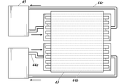
- the light irradiation apparatus used in the present invention has a water channel inside the pattern formation object mounting table as a water-cooling cooling function, introduces cooling water from one of the pattern formation object mounting tables, and It is preferable that a cooling function is provided with a plurality of water channels that flow the cooling water in one direction through the pattern forming body mounting table and discharge it to the other.
- FIG. 9 shows a specific example of the water channel provided inside the pattern forming body mounting table.
- a plurality of water channels 44b through which cooling water supplied from the water channel 44a flows are formed in one direction from one side of the pattern forming body mounting table to the other inside the pattern forming body mounting table.
- Cooling water flows in one direction through this water channel, and cools the heat generated in the mask and the organic EL element by ultraviolet irradiation.
- the water that has absorbed heat at the pattern forming body mounting table is discharged from the water channel 44c and sent to the chiller unit 45, where heat is exchanged inside the chiller unit 45, and the cooling water whose temperature has been lowered is supplied to the pattern forming body mounting table. Will be supplied again.
- the cooling water circulates inside the chiller unit and the pattern forming body mounting table.
- a plurality of chiller units may be provided according to the cooling capacity of the chiller.
- the water temperature introduced to the pattern forming body mounting table is preferably 30 ° C. or less as long as the organic EL element and the mask are not condensed. A range of 10 to 20 ° C. is more preferable.
- the cooling water flowing through the water channel 44b is made one-way, the cooling water that has absorbed heat and has risen in temperature can be discharged to the outside of the pattern forming body mounting table at the shortest distance. This is preferable because the cooling effect is higher than when reciprocating in the mounting table.
- the light irradiation device used in the present invention preferably includes a gas flow generation unit that blows gas onto the mask.
- the gas flow generation unit 10 is arranged at a position facing the upper surface of the mask 14 so that a gas such as air is blown in parallel to the mask 14 and toward the center of the mask 14 through the gap WD between the mask 14 and the cover 9. ing.
- the gas blown by the gas flow generator is not particularly limited as long as it can cool the mask and does not impair the effects of the present invention.
- air, nitrogen gas, etc. Can be suitably used.
- the gas flow generation unit 10 is arranged at a position opposite to the upper surface of the mask 14 so that the gas can be blown in parallel with the mask 14, and as a result, the blown gas flow 11 travels on the mask 14 without unevenness and the center of the mask. It is possible to join at the part.
- spraying in parallel means spraying at an angle within ⁇ 2 ° with respect to the plane of the mask 14.
- the air blown to the mask merges at the center of the mask 14.
- the gas flow generation part 10 is arrange
- the gap 12 between the cover 9 and the gas flow generating unit 10 is not particularly limited as long as air is efficiently blown onto the mask, but is preferably within a range of 10 to 200 mm. More preferably, it is in the range of 50 to 100 mm.
- the length of the gas flow generating part is preferably the same as or larger than the width of the cover on the side to be sprayed.
- the pair of gas flow generation units 10 is preferably disposed at a symmetrical position with respect to the central portion of the mask 14.
- the gas flow generation unit 10 includes a slit-shaped or nozzle-shaped sprayed portion. It is more preferable to have a slit-shaped spraying part. Furthermore, it is more preferable that the slit-like spraying part is one that blows gas in a line shape and cools the mask surface. This is because the mask can be cooled uniformly when the gas blown out is in a line shape.
- a nozzle provided with a nozzle-like spraying part can be used instead of the slit-like spraying part.
- the number of nozzles should be large, and the number of nozzles may be one at intervals of 5 to 20 mm. preferable.
- the size of the nozzle diameter can be adjusted as appropriate.
- a commercially available product can be used as the slit-shaped spraying part used for the spraying part.
- a layered airflow generator 750 manufactured by Sanwa Enterprise Co., Ltd. or a blower knife air nozzle manufactured by Spraying Systems Japan, Inc. can be used.
- the amount of air blown from the pair of blowing parts is preferably the same.
- the air volume can be 1000 to 4000 L / min.
- the gas flow generator is preferably connected to an air compressor. According to the irradiation light quantity of an ultraviolet-ray, it can adjust to a desired air volume and a wind speed suitably.
- a known air compressor can be used.
- the air to be blown is temperature-adjusted. If necessary, the cooling efficiency can be increased by using air whose temperature is adjusted to about 5 to 15 ° C., for example.
- having such a gas flow generation unit can efficiently cool the organic EL sheet and the mask by blowing gas on the mask, and has high irradiance. Since the influence of the heat accompanying a case can be reduced suitably, it is preferable.
- the cover has a function of preventing a reduction in the amount of ultraviolet light emitted from the light source unit and irradiating the mask with a uniform amount of light. Therefore, it is preferable that the inner surface is covered with a reflective material. Since the reflective material is resistant to heat and durable, a metal material can be used. For example, aluminum is preferably used because it is lightweight. If the light source part is attached to the upper part of the cover and has a gap with the mask at the lower end, the height and the bottom area are not particularly limited, and the size of the organic EL sheet that irradiates ultraviolet rays is not limited. It can be set accordingly. The bottom surface is preferably larger than the pattern formation area to be fabricated. The height of the cover can be adjusted as appropriate based on the amount of ultraviolet light, unevenness in the amount of irradiation light, and the like. For example, it can be about 0.5 to 5 m.
- the organic EL device includes one or a plurality of organic functional layers between at least a pair of electrodes.
- the organic functional layer in the present invention refers to a layer containing an organic compound. Examples thereof include a hole injection layer, a hole transport layer, a light emitting layer (including a blue light emitting layer, a green light emitting layer, and a red light emitting layer), an electron transport layer, and an electron injection layer.
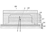
- the organic EL element according to the present invention can take various configurations, and an example is shown in FIG. Note that the aspect ratio is not accurate for the sake of illustration in FIG.
- the organic EL element 100 includes an organic functional layer unit 117 (a hole injection layer 117a, a hole transport layer 117b, a light emitting layer) having a light emitting layer on the first electrode 116 serving as an anode.
- 117c, an electron transport layer 117d, an electron injection layer 117e), and a second electrode 118 serving as a cathode are laminated, and further, a base material 102, a hard coat layer 103, a first gas barrier layer 104, and a second gas barrier layer 105 are formed.
- the gas barrier film 101 including the sealing resin layer 119 and the sealing member 120 are solid-sealed.
- the 1st electrode 116 used as an anode is comprised as a translucent electrode.
- the organic functional layer unit 117 is sandwiched between the first electrode 116 and the second electrode 118 becomes a light emitting region in the organic EL element 100.
- the organic EL element 100 is configured as a bottom emission type in which generated light (hereinafter also referred to as “light emission light h”) is extracted from at least the gas barrier film 101 side.
- a sealing member 120 is bonded on one surface of the gas barrier film 101 via a sealing resin layer 119 that covers the first electrode 116, the organic functional layer unit 117, and the second electrode 118. By doing so, it is solid-sealed.
- an uncured resin material is applied to the bonding surface of the sealing member 120 or a plurality of locations of the second gas barrier layer 105 and the second electrode 118 of the gas barrier film 101.
- the gas barrier film 101 and the sealing member 120 are integrated by thermocompression bonding with the resin material interposed therebetween.
- the organic EL element 100 according to the present invention is not limited to the bottom emission type, and may be a top emission type configuration in which light is extracted from the second electrode 118 side or a dual emission type configuration in which light is extracted from both sides. . If the organic EL element 100 is a top emission type, a transparent material is used for the second electrode 118 and the emitted light h is extracted from the second electrode 118 side. Further, when the organic EL element 100 is a double-sided light emitting type, a transparent material is used for the second electrode 118 and the emitted light h is extracted from both sides. In addition, a well-known thing can be used for the material used for each layer which comprises an organic EL element.
- the method for producing an organic electroluminescence element of the present invention is a method for producing an organic electroluminescence element for producing a pattern-formed organic electroluminescence element, wherein an edge (edge part) of the pattern is in the range of 10 to 300 ⁇ m. It can employ
- the brightness of the pattern edge portion moves from the center side of the light emitting portion toward the non-light emitting portion within a range of 10 to 300 ⁇ m. It is possible to manufacture an organic EL element having a luminance distribution in which the brightness decreases.
- the edge part of the light emission pattern refers to the side of the light emission pattern formed by the light shielding part in the mask.
- anode is formed on a substrate using a mask.
- each of the evaporation crucibles is filled with a hole injection material, a hole transport material, a host compound and a dopant for the light emitting layer, an electron transport material, and an electron injection material in an optimum amount for device fabrication.
- the evaporation crucible containing the hole injecting material is energized and heated to deposit the hole injecting material on the substrate to provide a hole injecting layer.
- the deposition crucible containing the hole transport material is energized and heated to deposit the hole transport material on the hole injection layer, thereby providing a hole transport layer.
- the deposition crucible containing the host compound and dopant of the light emitting layer is energized and heated, and the host compound and dopant of the light emitting layer are co-deposited on the hole transport layer to provide a light emitting layer.
- the deposition crucible containing the hole blocking material is energized and heated to deposit the hole blocking material on the light emitting layer, thereby providing a hole blocking layer.
- the evaporation crucible containing the electron transport material is energized and heated to deposit the electron transport material on the hole blocking layer, thereby providing an electron transport layer.
- the deposition crucible containing the electron injection material is energized and heated to deposit the electron injection material on the electron transport layer, thereby providing an electron injection layer.
- an organic functional layer can be formed.
- aluminum or the like is deposited on the electron injection layer to provide a cathode.
- the deposition surface side is covered with a sealing material such as an epoxy resin, and further covered with an aluminum foil to form a protective film, followed by curing. Note that all the operations up to here are preferably performed in a glove box (in an atmosphere of high-purity nitrogen gas having a purity of 99.999% or more) in a nitrogen atmosphere without bringing the element into contact with the air.
- an organic EL element can be produced. Such an organic EL element is cut into a predetermined size during patterning. The patterning of the organic EL element can be performed as described above. Moreover, the manufacturing method of an organic EL element is not limited to the said method, A well-known method can be used. The embodiments to which the present invention can be applied are not limited to the above-described embodiments, and can be appropriately changed without departing from the spirit of the present invention.
- the present invention is not limited to this, and continuous light may be irradiated.
- the said light irradiation apparatus was demonstrated as what has a cover, the light irradiation apparatus which does not have a cover may be sufficient.
- the method for producing a pattern-formed body of the present invention can suppress deformation of a mask used for patterning, and can be suitably used for patterning a light-emitting body such as an organic EL element.
Landscapes
- Engineering & Computer Science (AREA)
- Manufacturing & Machinery (AREA)
- Electroluminescent Light Sources (AREA)
Abstract
本発明の課題は、寸法精度が高い発光パターン形成用マスク及び発光パターンを有する有機エレクトロルミネッセンス素子の製造方法を提供することである。 本発明の発光パターン形成用マスクは、有機エレクトロルミネッセンス素子の有機機能層にマスクを通して光照射し、発光部の発光パターンを形成するための発光パターン形成用マスクであって、前記光照射に用いる光照射装置のコリメーション半角をθとしたとき、前記マスクの面内方向の前記マスクの遮光部の端部の位置を、形成するパターンのサイズから下記式(I)を満たす距離εの位置に一律に広げたものであることを特徴とする。 式(I):0<ε≦3×t×tanθ (式中、tはマスクから有機機能層までの空気換算長を表す。)
Description
本発明は、発光パターン形成用マスク及び有機エレクトロルミネッセンス素子の製造方法に関する。特に、本発明は、寸法精度の高いパターニングが可能な発光パターン形成用マスク等に関する。
現在、薄型の発光デバイスとして有機発光パネルが注目されている。例えば、有機材料のエレクトロルミネッセンス(Electroluminescence:EL)を利用した有機発光素子(以下「有機EL素子」ともいう。)は、数V~数十V程度の低電圧で発光が可能な薄膜型の完全固体パネルであり、低電力で高い輝度を得ることができ、視認性、応答速度、寿命、消費電力の点で優れ、薄型、軽量にできるといった多くの優れた特徴を有している。このため、有機EL素子をパネルとして用いた各種ディスプレイや、そのバックライト、看板や非常灯等の表示板、照明光源等の面発光体が近年注目されている。
有機ELパネルをディスプレイ用途に用いるため、パターニングされた有機EL素子を製造する方法として、基材上に積層された有機EL素子の有機機能層に対して紫外線を照射し、当該照射部分を劣化させることで、非発光領域を有する発光パターンを形成する有機ELパネルの製造方法が開示されている(例えば、特許文献1参照。)。この現象には、国際公開第2014/175135号に記載のとおり相反則不軌特性があり、同じ積算光量でも照射パワー密度(放射照度)が高い方が、反応が高速になることが知られている。
したがって、有機EL素子にパターニングを行う場合、できるだけ高放射照度にした方がタクトタイムを短縮でき、生産性を向上できる。しかし、高放射照度化と照射光の平行光化はトレードオフの関係にあり、高放射照度にするにはコリメーション半角を大きくする必要があるため、非平行光となってしまう。
有機EL素子が完成した後にパターニングを行う場合、パターン形成用のマスクの遮光膜を有機EL素子に密着させても基材の厚さの分、遮光膜と有機EL素子の有機機能層が離れた状態になる。このように有機機能層とマスクの遮光膜が密着していない場合、入射角が0°よりも大きい光はマスクの遮光膜の下側に潜り込み、パターンずれが発生してしまう。
有機EL素子が完成した後にパターニングを行う場合、パターン形成用のマスクの遮光膜を有機EL素子に密着させても基材の厚さの分、遮光膜と有機EL素子の有機機能層が離れた状態になる。このように有機機能層とマスクの遮光膜が密着していない場合、入射角が0°よりも大きい光はマスクの遮光膜の下側に潜り込み、パターンずれが発生してしまう。
また、半導体や液晶素子の回路パターンを近接光照射(プロキシミティ露光)で形成する場合、マスクの遮光膜のエッジで発生した回折光が干渉し、数μm~nmオーダーの線幅に対して正確なパターニングができない問題がある。
例えば、特許文献2及び特許文献3には、正確なパターニングをするための補正方法が開示されているが、複雑であるため、さらに簡便な方法が求められている。
例えば、特許文献2及び特許文献3には、正確なパターニングをするための補正方法が開示されているが、複雑であるため、さらに簡便な方法が求められている。
本発明は、上記問題・状況に鑑みなされたものであり、その解決課題は、寸法精度が高い発光パターン形成用マスク及び発光パターンを有する有機エレクトロルミネッセンス素子の製造方法を提供することである。
本発明に係る上記課題を解決すべく、上記問題の原因等について検討した結果、発光パターン形成用マスクの遮光部の端部の位置が、形成するパターンのサイズから所定の関係を満たす距離εの位置に一律に広げられたものを使用することで、本発明の上記課題を解決することができることを見いだし、本発明に至った。
すなわち、本発明に係る課題は、以下の手段により解決される。
すなわち、本発明に係る課題は、以下の手段により解決される。
1.有機エレクトロルミネッセンス素子の有機機能層にマスクを通して光照射し、発光部の発光パターンを形成するための発光パターン形成用マスクであって、
前記光照射に用いる光照射装置のコリメーション半角をθとしたとき、前記マスクの面内方向の前記マスクの遮光部の端部の位置を、形成するパターンのサイズから下記式(I)を満たす距離εの位置に一律に広げたものであることを特徴とする発光パターン形成用マスク。
式(I):0<ε≦3×t×tanθ
(式中、tはマスクから有機機能層までの空気換算長を表す。)
前記光照射に用いる光照射装置のコリメーション半角をθとしたとき、前記マスクの面内方向の前記マスクの遮光部の端部の位置を、形成するパターンのサイズから下記式(I)を満たす距離εの位置に一律に広げたものであることを特徴とする発光パターン形成用マスク。
式(I):0<ε≦3×t×tanθ
(式中、tはマスクから有機機能層までの空気換算長を表す。)
2.第1項に記載の発光パターン形成用マスクを使用して、有機エレクトロルミネッセンス素子の有機機能層に光照射により発光パターンを形成することを特徴とする有機エレクトロルミネッセンス素子の製造方法。
3.前記有機エレクトロルミネッセンス素子の前記発光部の発光パターンの端部が、10~300μmの範囲内で輝度分布を有することを特徴とする第2項に記載の有機エレクトロルミネッセンス素子の製造方法。
本発明の手段によれば、寸法精度が高い発光パターン形成用マスク及び発光パターンを有する有機エレクトロルミネッセンス素子の製造方法を提供することができる。
本発明の効果の発現機構又は作用機構については、明確にはなっていないが、以下のように推察している。
非平行光を使用することで平行光よりも高い照度で光照射することができるが、入射角が0°よりも大きい光はマスクの遮光部の下側に潜り込み、パターンずれが発生してしまう。しかし、有機EL素子の発光パターンは目視レベルの数十μm以上であればよいため回折の影響を考慮する必要はなく、簡易な補正ルールで発光パターン形成用マスクを設計することができ、目視レベルで十分なパターン精度を確保できたものと推察している。
非平行光を使用することで平行光よりも高い照度で光照射することができるが、入射角が0°よりも大きい光はマスクの遮光部の下側に潜り込み、パターンずれが発生してしまう。しかし、有機EL素子の発光パターンは目視レベルの数十μm以上であればよいため回折の影響を考慮する必要はなく、簡易な補正ルールで発光パターン形成用マスクを設計することができ、目視レベルで十分なパターン精度を確保できたものと推察している。
本発明の発光パターン形成用マスクは、有機エレクトロルミネッセンス素子の有機機能層にマスクを通して光照射し、発光部の発光パターンを形成するための発光パターン形成用マスクであって、前記光照射に用いる光照射装置のコリメーション半角をθとしたとき、前記マスクの面内方向の前記マスクの遮光部の端部の位置を、形成するパターンのサイズから前記式(I)を満たす距離εの位置に一律に広げたものであることを特徴とする。この特徴は、各請求項に係る発明に共通する又は対応する技術的特徴である。
本発明の有機エレクトロルミネッセンス素子の製造方法は、発光パターン形成用マスクを使用して、有機エレクトロルミネッセンス素子の有機機能層に光照射により発光パターンを形成することを特徴とする。これにより、寸法精度の高い発光パターンを有する有機エレクトロルミネッセンス素子を提供することができる。
また、本発明の実施態様としては、前記有機エレクトロルミネッセンス素子の前記発光部の発光パターンの端部が、10~300μmの範囲内で輝度分布を有することが、視感に訴える大抵のパターンを再現できる点で好ましい。
《発光パターン形成用マスク》
本発明の発光パターン形成用マスク(以下、単に「マスク」ともいう。)は、有機エレクトロルミネッセンス素子の有機機能層にマスクを通して光照射し、発光部の発光パターンを形成するための発光パターン形成用マスクであって、前記光照射に用いる光照射装置のコリメーション半角をθとしたとき、前記マスクの面内方向の前記マスクの遮光部の端部の位置を、形成するパターンのサイズから下記式(I)を満たす距離εの位置に一律に広げたものであることを特徴とする。
式(I):0<ε≦3×t×tanθ
式中、tはマスクから有機機能層までの空気換算長を表す。
本発明のマスクは、紫外線や可視光の透過光量を変えることができる公知のマスク材料を用いて作製することができる。これを用いて有機EL素子に光照射することにより、発光パターンを有する有機ELパネルを作製することができる。
本発明の発光パターン形成用マスク(以下、単に「マスク」ともいう。)は、有機エレクトロルミネッセンス素子の有機機能層にマスクを通して光照射し、発光部の発光パターンを形成するための発光パターン形成用マスクであって、前記光照射に用いる光照射装置のコリメーション半角をθとしたとき、前記マスクの面内方向の前記マスクの遮光部の端部の位置を、形成するパターンのサイズから下記式(I)を満たす距離εの位置に一律に広げたものであることを特徴とする。
式(I):0<ε≦3×t×tanθ
式中、tはマスクから有機機能層までの空気換算長を表す。
本発明のマスクは、紫外線や可視光の透過光量を変えることができる公知のマスク材料を用いて作製することができる。これを用いて有機EL素子に光照射することにより、発光パターンを有する有機ELパネルを作製することができる。
[マスクの設計方法]
光照射装置から照射される紫外光や可視光を非平行光とした場合、マスクへの入射角が0°(マスクを有する平面に対して垂直方向を0°とする。)からθまでの様々な光線がミックスされて有機EL素子に照射される。ここで、最大入射角θをコリメーション半角と呼ぶ。
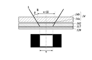
図1Aに示すように有機EL素子の基材にマスクの遮光部を密着させて光照射する場合でも、基材に厚さがあるため入射角が0°でない光線は遮光部の下側に潜り込んで有機機能層に達する。なお、マスクの基材や有機EL素子の基材による光線の屈折は省略してある。入射角がコリメーション半角の光線が潜り込む量をδとすると光照射後の発光パターン(明部)はそのエッジがマスク遮光部のエッジ位置よりδだけ内側にずれたパターンとなり、パターン幅としては2δ細くなってしまう。
光照射装置から照射される紫外光や可視光を非平行光とした場合、マスクへの入射角が0°(マスクを有する平面に対して垂直方向を0°とする。)からθまでの様々な光線がミックスされて有機EL素子に照射される。ここで、最大入射角θをコリメーション半角と呼ぶ。
図1Aに示すように有機EL素子の基材にマスクの遮光部を密着させて光照射する場合でも、基材に厚さがあるため入射角が0°でない光線は遮光部の下側に潜り込んで有機機能層に達する。なお、マスクの基材や有機EL素子の基材による光線の屈折は省略してある。入射角がコリメーション半角の光線が潜り込む量をδとすると光照射後の発光パターン(明部)はそのエッジがマスク遮光部のエッジ位置よりδだけ内側にずれたパターンとなり、パターン幅としては2δ細くなってしまう。
すなわち、マスクのパターン(マスクの遮光部が貼られている部分)を所望のパターン(原図)と同じサイズで作製してしまうと、有機EL素子に形成される実際のパターンは所望のパターンのサイズとは異なってしまう問題がある。
そこで、遮光部エッジ位置を原図のエッジ位置からδだけ広げ、遮光部の幅をw+2δとすれば、発光パターンの幅を原図と同じ幅wとすることができる(図1B参照。)。
そこで、遮光部エッジ位置を原図のエッジ位置からδだけ広げ、遮光部の幅をw+2δとすれば、発光パターンの幅を原図と同じ幅wとすることができる(図1B参照。)。
本発明の発光パターン形成用マスクは、光の回折の影響を無視できるパターンサイズに適用するので、入射角θの光線の潜り込み量は幾何光学よりt×tanθと考えることができる。
式(II):δ=t×tanθ
ここで、tは遮光部から有機機能層までの空気換算長で、基材の厚さをts、屈折率をnとした場合、下記式(III)を用いて求めることができる。
式(III):t=ts/n
式(II):δ=t×tanθ
ここで、tは遮光部から有機機能層までの空気換算長で、基材の厚さをts、屈折率をnとした場合、下記式(III)を用いて求めることができる。
式(III):t=ts/n
近接光照射の場合にはさらに有機EL素子とマスクのギャップが加わる。ここで、マスク遮光部のエッジ位置の補正量をεとした時、必ずしもε=t×tanθとはならない。
この理由について説明すると、非平行光とした場合でも、光照射面上で様々な入射角の光線を重なるようにして放射照度が一様分布になるようにしている。しかし、マスク遮光部では一部の方向からの光線のみが遮光部の下に潜り込むために光線密度が低下し、放射照度が落ちる。遮光部エッジから内側に行くほど放射照度の低下が大きくなるため、有機機能層の反応に必要な光量が得られず、反応が不十分となり非発光部となるのはt×tanθよりも外側になる。
この理由について説明すると、非平行光とした場合でも、光照射面上で様々な入射角の光線を重なるようにして放射照度が一様分布になるようにしている。しかし、マスク遮光部では一部の方向からの光線のみが遮光部の下に潜り込むために光線密度が低下し、放射照度が落ちる。遮光部エッジから内側に行くほど放射照度の低下が大きくなるため、有機機能層の反応に必要な光量が得られず、反応が不十分となり非発光部となるのはt×tanθよりも外側になる。
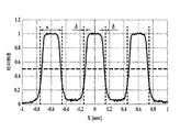
図2に実際に作製した有機EL素子の発光パターンの顕微鏡写真を示す。これは、ハーフピッチ0.3mmのライン&スペースで長さ2mmのパターンを、補正をしていないマスクで作製した有機EL素子を発光させた場合を表している。すなわち、幅0.3mmの遮光部を0.6mmピッチで三つ配置した発光パターンである。
この時に用いた光照射装置のコリメーション半角θは45°で、放射照度4W/cm2にて積算光照射時間6分で光照射した。この発光パターンのx方向の相対輝度分布を図3Aに示す。
非平行光での光照射のため発光パターンの端部(エッジ部)は傾斜した輝度分布を有しており、発光部の線幅を相対輝度0.5で規定すると線幅は0.26mmと遮光部幅0.3mmより細く、δ=20μmとなっている。
非平行光での光照射のため発光パターンの端部(エッジ部)は傾斜した輝度分布を有しており、発光部の線幅を相対輝度0.5で規定すると線幅は0.26mmと遮光部幅0.3mmより細く、δ=20μmとなっている。
この有機EL素子の基材は、厚さts=130μm、n=1.7なので、t=76μmとなり、θが45°であるためt×tanθ=76μmとなるが、実際の細り量δは20μmと半分以下である。
また、暗部の相対輝度が0近辺まで落ちておらず、積算光照射時間が足りず反応がいまだ十分でない状態である。
また、暗部の相対輝度が0近辺まで落ちておらず、積算光照射時間が足りず反応がいまだ十分でない状態である。
次に積算光照射時間10分で光照射した場合を図3Bに示す。この場合の明部の細り量δは30μmとなり、発光部幅がさらに細くなった。暗部の相対輝度は0付近まで落ちており、ほぼ非発光状態になっている。このように同じ放射照度であれば積算光照射時間を長くするほど明部の細り量が増え、最終的にはt×tanθまで達する。したがって、補正量εは目標とする明部と暗部のコントラスト(輝度比)をどこに設定するかで変わってくる。目標輝度比が低ければεも小さくて済むし、高くするほどεはt×tanθに近づく。よって、0<ε≦t×tanθの範囲で適宜設定することが好ましい。
さらに、放射照度を高めた場合、マスクの遮光部が紫外光や可視光を吸収し発熱してマスクに熱変形が生じることが懸念される。この対策として紫外光や可視光の反射率の高い遮光部を用いた場合には、図4に示すように遮光部と有機EL素子の金属電極の間で多重反射が発生し、光線の潜り込み量がさらに増加してしまう。
遮光部での内部反射が2回以上になると減衰のためパターンが形成されるほどの放射照度とならないので、1回反射まで考慮する必要がある。この場合、補正量εは最大で3×t×tanθとなる。したがって、εの範囲は0<ε≦3×t×tanθとなる。
遮光部での内部反射が2回以上になると減衰のためパターンが形成されるほどの放射照度とならないので、1回反射まで考慮する必要がある。この場合、補正量εは最大で3×t×tanθとなる。したがって、εの範囲は0<ε≦3×t×tanθとなる。
[マスクの設計方法]
次に具体的なマスクのパターン設計方法について説明する。コリメーション半角がマスク面内のどの方向も同じ場合には、どの方向も所望のパターン(原図)のエッジ部をεだけ広げたものをマスクパターンとすればよい。
例えば、図5に示すように半径εの円の中心を図中点線で示した原図のエッジに多数配置し、これらの円の外側包絡線で囲まれた部分をマスクの遮光部とすればよい。
次に具体的なマスクのパターン設計方法について説明する。コリメーション半角がマスク面内のどの方向も同じ場合には、どの方向も所望のパターン(原図)のエッジ部をεだけ広げたものをマスクパターンとすればよい。
例えば、図5に示すように半径εの円の中心を図中点線で示した原図のエッジに多数配置し、これらの円の外側包絡線で囲まれた部分をマスクの遮光部とすればよい。
一方、コリメーション半角がマスク面内で方向によって異なる場合にはその面内分布形状に応じて、方向により補正量εを変える必要がある。
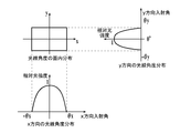
具体的には、例えば、コリメーション半角がマスク面内のx方向とy方向で異なる場合、図6のようにマスク面内の光線角度分布が長方形となる。x方向とy方向のコリメーション半角を各々θx、θyとして、各々の補正量をεx、εyとすると、図7のようにx方向、y方向の長さが各々2εx、2εyの長方形の中心を原図パターンのエッジに配置し、その外側包絡線を補正パターンとすればよい。
より一般的には、面内方向φに対してコリメーション半角θが異なる場合、面内方向φの補正量をε(φ)とした時、φに対する長さr=ε(φ)の軌跡形状の中心を原図パターンのエッジに配置し、その外側包絡線をマスクの補正パターンとすればよい。
具体的には、例えば、コリメーション半角がマスク面内のx方向とy方向で異なる場合、図6のようにマスク面内の光線角度分布が長方形となる。x方向とy方向のコリメーション半角を各々θx、θyとして、各々の補正量をεx、εyとすると、図7のようにx方向、y方向の長さが各々2εx、2εyの長方形の中心を原図パターンのエッジに配置し、その外側包絡線を補正パターンとすればよい。
より一般的には、面内方向φに対してコリメーション半角θが異なる場合、面内方向φの補正量をε(φ)とした時、φに対する長さr=ε(φ)の軌跡形状の中心を原図パターンのエッジに配置し、その外側包絡線をマスクの補正パターンとすればよい。
ところで、非平行光で照射した場合、発光部のエッジは輝度分布が傾きを持っているので、この傾斜部の幅によって光照射パターンの解像度の設計限界が決まる。傾斜部の幅をdとした場合、右傾斜と左傾斜の上端が接した状態が明部の解像限界となり、下端が接した状態が暗部の解像限界となる。相対輝度50%で幅を規定した場合、明部暗部とも解像限界幅はdとなる。dは最大でt×tanθとなるので、有機EL素子の基材の厚さが薄く、コリメーション半角が小さいほど解像度を高められる。
しかし、コリメーション半角を小さくすると放射照度を上げることができなくなってしまう。有機EL素子の照度不軌特性を利用して照射時間を短縮するには1W/cm2以上の照度が好ましく、この照度でコリメーション半角をできるだけ小さくなるように設計した結果、コリメーション半角は23°まで小さくできることが分かった。
このコリメーション半角で、有機EL素子の基材の厚さを例えば25μm(n=1.7)まで薄型化した場合には、d=t×tanθ=6μmとなり、かなりの解像度を確保できる。
一方、タクトタイム優先とし、コリメーション半角の増大を許容した場合、例えばθ=50°、基材厚500μmの場合にはd=351μmとなり、ハーフピッチ0.35mmが解像限界となる。ハーフピッチ0.3mm程度の解像度であれば、視感に訴える大抵のパターンは再現できるので、エッジの輝度分布の傾斜幅は10~300μmの範囲内が望ましい。
しかし、コリメーション半角を小さくすると放射照度を上げることができなくなってしまう。有機EL素子の照度不軌特性を利用して照射時間を短縮するには1W/cm2以上の照度が好ましく、この照度でコリメーション半角をできるだけ小さくなるように設計した結果、コリメーション半角は23°まで小さくできることが分かった。
このコリメーション半角で、有機EL素子の基材の厚さを例えば25μm(n=1.7)まで薄型化した場合には、d=t×tanθ=6μmとなり、かなりの解像度を確保できる。
一方、タクトタイム優先とし、コリメーション半角の増大を許容した場合、例えばθ=50°、基材厚500μmの場合にはd=351μmとなり、ハーフピッチ0.35mmが解像限界となる。ハーフピッチ0.3mm程度の解像度であれば、視感に訴える大抵のパターンは再現できるので、エッジの輝度分布の傾斜幅は10~300μmの範囲内が望ましい。
[光照射装置]
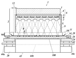
図8に示す光照射装置1は、主には、光照射部2と、被パターン形成体載置台43等により構成されている。
光照射部2は、光源部6と、レンズアレイ7、カバー9等を備えることが好ましい。
光源部6は、光源基板4上に、紫外線を出射する光源(LED)5として、例えば、発光波長が365nmや385nmのUV-LEDを平面状に並列配置し、光源5から出射した光を、レンズアレイ7で所定の広がり角の光束に整形し、反射導光するカバー9を通じて、その下部に位置するマスク14を介して、シート状の有機EL素子(有機ELシート)100に照射する。有機ELシートは、被パターン形成体載置台43に保持されている。レンズアレイ7はレンズアレイ支持体8により光源部に固定される。
図8に示す光照射装置1は、主には、光照射部2と、被パターン形成体載置台43等により構成されている。
光照射部2は、光源部6と、レンズアレイ7、カバー9等を備えることが好ましい。
光源部6は、光源基板4上に、紫外線を出射する光源(LED)5として、例えば、発光波長が365nmや385nmのUV-LEDを平面状に並列配置し、光源5から出射した光を、レンズアレイ7で所定の広がり角の光束に整形し、反射導光するカバー9を通じて、その下部に位置するマスク14を介して、シート状の有機EL素子(有機ELシート)100に照射する。有機ELシートは、被パターン形成体載置台43に保持されている。レンズアレイ7はレンズアレイ支持体8により光源部に固定される。
レンズアレイ7から出射した照射光Lは、内面が反射面となっているカバー内部に閉じ込められ、光量の低下を防ぎ、かつ均一な光量でマスク14に光照射される。
また、光照射エリア周辺部の光量を確保するためには、カバー下端とマスクの間隙(WD)はできるだけ狭い方が良く、5mm程度が望ましい。この間隙であれば、マスクに層状の流体を一様に吹き付けることができる。
また、光照射エリア周辺部の光量を確保するためには、カバー下端とマスクの間隙(WD)はできるだけ狭い方が良く、5mm程度が望ましい。この間隙であれば、マスクに層状の流体を一様に吹き付けることができる。
光源5は、コントローラ(不図示)により点灯、消灯や点灯時の照射出力、照射時間が制御され間欠光照射を行う。図8の説明においては、広がり角整形にレンズアレイ7を用いたが、複合放物面集光器のような集光ミラーを用いてもよい。
また、光源基板4の上部には、光源5の発光により生じた熱を、外部に放出するための放熱板3を具備していることが好ましい。このような放熱板3を設置することにより、光源部6の温度上昇を抑制することができる。
光照射部2全体から出射される光(照射光L)の照射エリアは有機ELシートの有機EL素子が配置されている領域全面をカバーできるエリアとなっている。すなわち、光源5を全て点灯させた場合には、一度に全ての有機EL素子をパターニングすることができる。
また、光源部6は、複数のLED光源を有しているため、有機ELシートのサイズ等に応じて複数のグループにわけて点灯を制御してもよいし、有機ELシートの光照射エリアを分割して光照射エリアに応じて複数のグループの光源を選択し点灯制御してもよい。光照射エリアを小さくすることによりマスクの熱変形をさらに抑制することができる。
なお、図8に示す例では、被パターン形成体載置台43に対して1台の光照射部2内の光源5を一斉又は順次点灯させる場合について説明したが、光照射部2よりも小型の光照射部を各光照射エリア上にステップ移動させたり、小型の光照射部を複数配置して各光照射エリアの光照射に応じて順次各光照射部2を発光させてもよい。
また、光源基板4の上部には、光源5の発光により生じた熱を、外部に放出するための放熱板3を具備していることが好ましい。このような放熱板3を設置することにより、光源部6の温度上昇を抑制することができる。
光照射部2全体から出射される光(照射光L)の照射エリアは有機ELシートの有機EL素子が配置されている領域全面をカバーできるエリアとなっている。すなわち、光源5を全て点灯させた場合には、一度に全ての有機EL素子をパターニングすることができる。
また、光源部6は、複数のLED光源を有しているため、有機ELシートのサイズ等に応じて複数のグループにわけて点灯を制御してもよいし、有機ELシートの光照射エリアを分割して光照射エリアに応じて複数のグループの光源を選択し点灯制御してもよい。光照射エリアを小さくすることによりマスクの熱変形をさらに抑制することができる。
なお、図8に示す例では、被パターン形成体載置台43に対して1台の光照射部2内の光源5を一斉又は順次点灯させる場合について説明したが、光照射部2よりも小型の光照射部を各光照射エリア上にステップ移動させたり、小型の光照射部を複数配置して各光照射エリアの光照射に応じて順次各光照射部2を発光させてもよい。
[マスク]
マスクは、有機EL素子に照射する光量を変える役割を有する。
マスク14は、一例として、基材14bと遮光部14aとの2層構成となっており、遮光部がマスクフレーム22側となるように、マスクアライメント機構部20に装着されることが好ましい。マスクアライメント機構部20は、例えば、中央に開口部を有する四角形状のマスクフレーム22と、マスクフレーム22の各辺上に設けられ、対向して配置された弾性体24と、弾性体24を固定する固定手段26と、を備えて構成されている。
弾性体24は、マスクフレーム22上に載置され、マスク14の側面と面接触することによりマスク14を側方から押圧して固定する。
また、マスクフレーム22の対向する1組の辺上に、少なくとも一対のマスク外れ防止規制板28を対向して配置させることが好ましい。
マスクは、有機EL素子に照射する光量を変える役割を有する。
マスク14は、一例として、基材14bと遮光部14aとの2層構成となっており、遮光部がマスクフレーム22側となるように、マスクアライメント機構部20に装着されることが好ましい。マスクアライメント機構部20は、例えば、中央に開口部を有する四角形状のマスクフレーム22と、マスクフレーム22の各辺上に設けられ、対向して配置された弾性体24と、弾性体24を固定する固定手段26と、を備えて構成されている。
弾性体24は、マスクフレーム22上に載置され、マスク14の側面と面接触することによりマスク14を側方から押圧して固定する。
また、マスクフレーム22の対向する1組の辺上に、少なくとも一対のマスク外れ防止規制板28を対向して配置させることが好ましい。
紫外線の透過光量を変えることができる公知の材料を用いて、基材上にネガ状のパターンを有するマスクを作製することができるが、特に、線膨張率の低い石英基板に紫外線吸収率が比較的低いクロム遮光部をパターン付与したものが、熱変形を抑制できる点で好ましい。このようなマスクを用い、有機EL素子に紫外線照射することにより、発光パターンを有する有機EL素子を作製することができる。
本発明においては、有機EL素子が冷却機能を有する被パターン形成体載置台に載置され、本発明のマスクが有機EL素子と所定の相対位置に位置決めされて、素子の上に密着配置されることが好ましい。これは、光が照射されることで発熱源となる遮光部の冷却効果を高めることができるためであり、具体的には、遮光部を有機EL素子に密着させることが好ましい。
(基材)
基材としては、素材として、特に限定されることがなく、例えば、光学用や基材用に用いられる公知のガラス素材を用いることができる。具体的には、アルミノシリケートガラス、ソーダライムガラス、ソーダアルミノケイ酸ガラス、アルミノボロシリケートガラス、ボロシリケートガラス、石英ガラス、チェーンシリケートガラス、結晶化ガラス等のガラスセラミック、リン酸系ガラス又はランタン系ガラス等を挙げることができる。
これらの中では、熱膨張率の低いものが好ましい。石英ガラス、ガラスセラミック及びボロシリケートガラス(例えば、ショット社製テンパックス フロート(登録商標))等の耐熱ガラスを好ましく用いることができる。マスクの厚さは特に制限はないが、3~10mmのものを用いることができる。
基材としては、素材として、特に限定されることがなく、例えば、光学用や基材用に用いられる公知のガラス素材を用いることができる。具体的には、アルミノシリケートガラス、ソーダライムガラス、ソーダアルミノケイ酸ガラス、アルミノボロシリケートガラス、ボロシリケートガラス、石英ガラス、チェーンシリケートガラス、結晶化ガラス等のガラスセラミック、リン酸系ガラス又はランタン系ガラス等を挙げることができる。
これらの中では、熱膨張率の低いものが好ましい。石英ガラス、ガラスセラミック及びボロシリケートガラス(例えば、ショット社製テンパックス フロート(登録商標))等の耐熱ガラスを好ましく用いることができる。マスクの厚さは特に制限はないが、3~10mmのものを用いることができる。
(遮光部)
遮光部は、光照射装置からの照射光を遮るものであればよく、特に限定するものではない。例えば、紫外光の反射率が高い遮光部としては、例えばクロム(Cr)を用いた薄膜が好ましい。純Crの場合、反射率が50%程度あるが、酸化クロム(CrO)で純Crを挟んだ構造とし、各膜厚を最適化することで紫外光の吸収率を抑えつつ、有機EL素子側の反射率を10%未満に抑えることが可能であり、このようなマスクの遮光部を選定することが望ましい。
遮光部は、光照射装置からの照射光を遮るものであればよく、特に限定するものではない。例えば、紫外光の反射率が高い遮光部としては、例えばクロム(Cr)を用いた薄膜が好ましい。純Crの場合、反射率が50%程度あるが、酸化クロム(CrO)で純Crを挟んだ構造とし、各膜厚を最適化することで紫外光の吸収率を抑えつつ、有機EL素子側の反射率を10%未満に抑えることが可能であり、このようなマスクの遮光部を選定することが望ましい。
[光照射部]
光照射部は、波長が100~410nmの範囲内の光を1W/cm2以上の放射照度で照射することが好ましい。
光照射部には、例えば紫外線を発光する光源が取り付けられている。光源としては、所望の紫外線光量を発光する光源であれば、特に制限はない。例えば、超高圧水銀灯、高圧水銀灯、低圧水銀灯、カーボンアーク、メタルハライドランプ、キセノンアークランプ、カーボンアークランプ、エキシマランプ、UV光レーザー等から発せられる100~410nmの範囲、好ましくは200~410nmの範囲の波長領域の紫外線や可視光を用いることができる。中でも、波長が350~410nmのLEDを複数備えていることが特に好ましい。これは、波長が350~410nmの光は、有機EL素子の発光効率低下の感度が高い紫外線及び可視光領域の波長の光であるため、タクトタイムをより短縮できるからである。
光照射部は、波長が100~410nmの範囲内の光を1W/cm2以上の放射照度で照射することが好ましい。
光照射部には、例えば紫外線を発光する光源が取り付けられている。光源としては、所望の紫外線光量を発光する光源であれば、特に制限はない。例えば、超高圧水銀灯、高圧水銀灯、低圧水銀灯、カーボンアーク、メタルハライドランプ、キセノンアークランプ、カーボンアークランプ、エキシマランプ、UV光レーザー等から発せられる100~410nmの範囲、好ましくは200~410nmの範囲の波長領域の紫外線や可視光を用いることができる。中でも、波長が350~410nmのLEDを複数備えていることが特に好ましい。これは、波長が350~410nmの光は、有機EL素子の発光効率低下の感度が高い紫外線及び可視光領域の波長の光であるため、タクトタイムをより短縮できるからである。
なお、パターニングを行うための積算照射量としては、有機EL素子の層構成、膜厚、サイズ等にもよるが、200~5000J/cm2の積算光量で照射することが、生産性が高く、正確なパターニングが行える観点から好ましい。また、間欠光照射における1パルス照射時の照射時間は、1~300秒の範囲内であることが好ましい。
光照射部としては、例えば、光源として、波長385nmのUV-LEDを使用し、これらを2次元状に配置し、LEDから出射した照射光をレンズアレイ7で所定のコリメーション半角となるように整形することで、レンズアレイ7の各レンズから出射した光が照射面で重なり合い、この結果、有機ELシートの広い面積に照射することができ、かつ、一様な照度分布とすることができる。
この場合、なお、LEDは不図示のコントローラにより点灯、消灯や点灯時の照射出力、照射時間が制御されたパルス光の間欠光照射を行うものであることが好ましい。
この場合、なお、LEDは不図示のコントローラにより点灯、消灯や点灯時の照射出力、照射時間が制御されたパルス光の間欠光照射を行うものであることが好ましい。
[放射照度]
光照射部は、波長が100~410nmの範囲内の光を1W/cm2以上の放射照度で照射するが、高輝度で高速パターニングを行うためには、放射照度は2W/cm2以上が好ましく、4W/cm2以上がより好ましい。さらに光照射エリア5000cm2以上でかつ、放射照度4W/cm2が、パターニングのタクトタイムの大幅な短縮と取り数を増大させることが可能となり、この結果、生産性を著しく向上できる点で好ましい。
また、光照射エリア内における前記波長が100~410nmの範囲内の光の放射照度が、当該光照射エリア内における前記放射照度の平均値に対し±10%の範囲内であることが好ましい。
光照射部は、波長が100~410nmの範囲内の光を1W/cm2以上の放射照度で照射するが、高輝度で高速パターニングを行うためには、放射照度は2W/cm2以上が好ましく、4W/cm2以上がより好ましい。さらに光照射エリア5000cm2以上でかつ、放射照度4W/cm2が、パターニングのタクトタイムの大幅な短縮と取り数を増大させることが可能となり、この結果、生産性を著しく向上できる点で好ましい。
また、光照射エリア内における前記波長が100~410nmの範囲内の光の放射照度が、当該光照射エリア内における前記放射照度の平均値に対し±10%の範囲内であることが好ましい。
<放射照度の分布>
本発明に用いる光照射装置は、光照射エリア内における前記波長の範囲内の光の放射照度(以下、単に「放射照度」ともいう。)が、当該光照射エリア内における放射照度の平均値に対し±10%の範囲内である。
本発明に用いる光照射装置は、光照射エリア内における前記波長の範囲内の光の放射照度(以下、単に「放射照度」ともいう。)が、当該光照射エリア内における放射照度の平均値に対し±10%の範囲内である。
(放射照度の分布の測定方法)
放射照度は、公知の測定器で測定することができ、例えば、波長範囲が300~410nmの場合、紫外線積算光量計「C9536-02」とセンサヘッド「H9958-02」(浜松ホトニクス株式会社製)を使用して、光照射エリアの縦、横に1~10mm間隔で測定することができる。
上述のようにして測定された、光照射エリア内における放射照度の分布から、光照射エリア内の波長の範囲内の光の放射照度の平均を計算することができる。
放射照度は、公知の測定器で測定することができ、例えば、波長範囲が300~410nmの場合、紫外線積算光量計「C9536-02」とセンサヘッド「H9958-02」(浜松ホトニクス株式会社製)を使用して、光照射エリアの縦、横に1~10mm間隔で測定することができる。
上述のようにして測定された、光照射エリア内における放射照度の分布から、光照射エリア内の波長の範囲内の光の放射照度の平均を計算することができる。
<コリメーション半角>
本発明に用いる光照射装置においては、前記光照射エリア内における前記波長が100~410nmの範囲内の光のコリメーション半角が、45°以下であることが好ましい。なお、1W/cm2以上の放射照度を実現するためには、23°以上のコリメーション半角を有する光を含むことが好ましい。
コリメーション半角とは、前述のとおりマスクに対する垂線Rと照射光Lとがなす角θのうち、最大のものをいう(図8参照)。コリメーション半角は、光源部から出射した光をレンズなどで整形することで調整できる。
本発明に用いる光照射装置においては、前記光照射エリア内における前記波長が100~410nmの範囲内の光のコリメーション半角が、45°以下であることが好ましい。なお、1W/cm2以上の放射照度を実現するためには、23°以上のコリメーション半角を有する光を含むことが好ましい。
コリメーション半角とは、前述のとおりマスクに対する垂線Rと照射光Lとがなす角θのうち、最大のものをいう(図8参照)。コリメーション半角は、光源部から出射した光をレンズなどで整形することで調整できる。
(レンズ)
コリメーション半角を調整するための、レンズとしては特に限定されず、例えば、レンズアレイの代わりに、複合放物面集光器のような集光ミラーを用いてもよい。複合放物面集光器であれば、部品コストを抑えることができるため好ましい。また、その他図示は省略するが、棒状シリンドリカルレンズ又はロッドレンズをLEDアレイの各列に配置し、続いて直交する方向に棒状シリンドリカルレンズやロッドレンズを配置して2次元方向のコリメーション角整形を行ってもよい。このようにすれば、光軸調整を各々一方向だけ行えばよく、調整工数を抑制できるため好ましい。
コリメーション半角を調整するための、レンズとしては特に限定されず、例えば、レンズアレイの代わりに、複合放物面集光器のような集光ミラーを用いてもよい。複合放物面集光器であれば、部品コストを抑えることができるため好ましい。また、その他図示は省略するが、棒状シリンドリカルレンズ又はロッドレンズをLEDアレイの各列に配置し、続いて直交する方向に棒状シリンドリカルレンズやロッドレンズを配置して2次元方向のコリメーション角整形を行ってもよい。このようにすれば、光軸調整を各々一方向だけ行えばよく、調整工数を抑制できるため好ましい。
(コリメーション半角の測定方法)
被パターン形成体載置台を光照射部から退避させ、ピンホールを被パターン形成体載置台の有機ELシートを載置する面と同じ高さに配置し、照射光をピンホールに照射し、ピンホールを通り抜けた光束をCCDカメラで観測、又はピンホールの下に配置した紫外線感光紙を照射し変色させ、その光束(変色部)の半径Mを計測する。ピンホールとCCD素子又は紫外線感光紙の間隔をDとした時、コリメーション半角はtan-1(M/D)にて算出される。ピンホールの径はφ0.5mm以下が望ましい。
被パターン形成体載置台を光照射部から退避させ、ピンホールを被パターン形成体載置台の有機ELシートを載置する面と同じ高さに配置し、照射光をピンホールに照射し、ピンホールを通り抜けた光束をCCDカメラで観測、又はピンホールの下に配置した紫外線感光紙を照射し変色させ、その光束(変色部)の半径Mを計測する。ピンホールとCCD素子又は紫外線感光紙の間隔をDとした時、コリメーション半角はtan-1(M/D)にて算出される。ピンホールの径はφ0.5mm以下が望ましい。
[光照射エリア]
光照射エリアとは、本発明に用いる光照射装置が照射する光の領域である。
光照射エリアの面積は、特に限定されないが、5000cm2以上であることが好ましい。この理由は次のとおりである。
光照射エリアとは、本発明に用いる光照射装置が照射する光の領域である。
光照射エリアの面積は、特に限定されないが、5000cm2以上であることが好ましい。この理由は次のとおりである。
ロール・to・ロール方式で有機EL素子を製造する場合、一般的にロールの幅は1m程度ある。パターニングする際は、これをロール巻き方向に600mm程度の長さにカットして、複数の有機EL素子を平面状に備えるシート状にして、これら複数の有機EL素子に対し、まとめて光を照射することが好ましい。
例えば、x方向のサイズが100cmでありy方向のサイズが60cmのサイズの有機ELシートに対して、複数の有機EL素子が内側90cm×54cmの領域に配置される。光照射エリアを30cm×18cm(=540cm2)とすれば、x方向に3ステップ、y方向に3ステップの合計9ステップと10ステップ以内で一つの有機ELシートに光を照射できる。このように大面積の光照射エリアとすることにより有機ELシートの状態での光照射が可能となり、複数の有機EL素子を一度にパターニングでき、スループットを向上できる。有機ELシートの全面を一括で光照射する場合には、90cm×54cm=4860cm2以上の光照射エリアが必要であることから、5000cm2以上の光照射エリアであることが好ましい。
例えば、x方向のサイズが100cmでありy方向のサイズが60cmのサイズの有機ELシートに対して、複数の有機EL素子が内側90cm×54cmの領域に配置される。光照射エリアを30cm×18cm(=540cm2)とすれば、x方向に3ステップ、y方向に3ステップの合計9ステップと10ステップ以内で一つの有機ELシートに光を照射できる。このように大面積の光照射エリアとすることにより有機ELシートの状態での光照射が可能となり、複数の有機EL素子を一度にパターニングでき、スループットを向上できる。有機ELシートの全面を一括で光照射する場合には、90cm×54cm=4860cm2以上の光照射エリアが必要であることから、5000cm2以上の光照射エリアであることが好ましい。
このような大面積の光照射エリアは、例えば、LEDの数を増やし、光源部の発光面積を拡大すれば実現可能であるが、この場合、本発明で用いられる光照射装置は、冷却機能を併せて備えていることが好ましい。これにより、1回の照射総光量が非常に高くなったとしても、マスクの遮光部の発熱を抑えることができる。
[被パターン形成体載置台]
本発明で用いられる光照射装置1は、有機エレクトロルミネッセンス素子を載置する被パターン形成体載置台43を備えることが好ましい。
被パターン形成体載置台は、有機エレクトロルミネッセンス素子を載置できるものであり、かつ、本発明の効果を阻害しないものであればよく、特に限定されないが、例えば、有機ELシート100を吸着固定できるものであることが好ましい。一般に、有機EL素子の基材としてポリエチレンテレフタレート(略称:PET)やポリエチレンナフタレート(略称:PEN)を用いた場合、有機ELシートはカールするなど変形しやすいが、有機ELシートを吸着固定できる被パターン形成体載置台であれば、シート全面を吸着することにより、平面性よく被パターン形成体載置台に固定でき、パターニングの光照射ボケを防止できる。
なお、被パターン形成体載置台の材質は、特に限定されない。ただし、被パターン形成体載置台が後述の水路44bを有する場合、被パターン形成体載置台は冷却台となるため、その材質は熱伝導率の高い金属が好ましく、具体的には、例えば、アルミニウムが使用できる。
本発明で用いられる光照射装置1は、有機エレクトロルミネッセンス素子を載置する被パターン形成体載置台43を備えることが好ましい。
被パターン形成体載置台は、有機エレクトロルミネッセンス素子を載置できるものであり、かつ、本発明の効果を阻害しないものであればよく、特に限定されないが、例えば、有機ELシート100を吸着固定できるものであることが好ましい。一般に、有機EL素子の基材としてポリエチレンテレフタレート(略称:PET)やポリエチレンナフタレート(略称:PEN)を用いた場合、有機ELシートはカールするなど変形しやすいが、有機ELシートを吸着固定できる被パターン形成体載置台であれば、シート全面を吸着することにより、平面性よく被パターン形成体載置台に固定でき、パターニングの光照射ボケを防止できる。
なお、被パターン形成体載置台の材質は、特に限定されない。ただし、被パターン形成体載置台が後述の水路44bを有する場合、被パターン形成体載置台は冷却台となるため、その材質は熱伝導率の高い金属が好ましく、具体的には、例えば、アルミニウムが使用できる。
また、複数の有機EL素子が備えられた有機ELシートに光を照射する場合には、被パターン形成体載置台が大型となり、かつ冷却水も流れるため質量が増してしまう。そのため、マスクとシートのアライメントはマスクが載置されたマスクフレームを被パターン形成体載置台の平面内の座標(X、Y、φ)で調整することが好ましい。
<冷却機能>
有機EL素子のパターニングを高速で行うために2W/cm2以上の非常に高い放射照度で光を照射した場合、マスクの遮光部(クロムなど)が紫外線を吸収し温度が上昇する。このため、被パターン形成体載置台が、冷却機能を有することが好ましい。これにより、マスクに熱変形が生じることを抑制でき、ひいては、光照射パターンのずれ発生や熱に弱い有機機能層が熱ダメージを受け性能が劣化してしまう問題の発生を防止できる。
有機EL素子のパターニングを高速で行うために2W/cm2以上の非常に高い放射照度で光を照射した場合、マスクの遮光部(クロムなど)が紫外線を吸収し温度が上昇する。このため、被パターン形成体載置台が、冷却機能を有することが好ましい。これにより、マスクに熱変形が生じることを抑制でき、ひいては、光照射パターンのずれ発生や熱に弱い有機機能層が熱ダメージを受け性能が劣化してしまう問題の発生を防止できる。
冷却機能としては、マスクを冷却できるものであればよく、特に限定されず、具体的には、例えば、水冷方式や、空気などの気体をマスクに吹き付けることなどが挙げられる。中でも、本発明で用いられる光照射装置は、水冷方式の冷却機能として、前記被パターン形成体載置台の内部に水路を備え、冷却水を被パターン形成体載置台の一方から導入し、前記被パターン形成体載置台内を一方向に前記冷却水を流して他方に排出する複数の水路を冷却機能として備えることが好ましい。
図9に、被パターン形成体載置台内部に備えられた水路の具体的な一例を示す。図9の例では、被パターン形成体載置台内部には、水路44aから供給される冷却水が流れる複数の水路44bが、被パターン形成体載置台の一方から他方に向けて一方向に貫通形成されている。この水路を一方向に冷却水が流れ、紫外線照射によりマスクや有機EL素子で発生した熱を冷却する。
被パターン形成体載置台で熱を吸収した水は水路44cから排出されてチラーユニット45に送られ、チラーユニット45内部にて熱交換され、水温を下げた冷却水が被パターン形成体載置台に再び供給される。このように図8の例では、冷却水はチラーユニットと被パターン形成体載置台内部を循環する。チラーユニットは、チラーの冷却能力に応じて複数設けてもよい。
なお、装置作動中は常時冷却機能を動作させておくことが好ましい。
また、被パターン形成体載置台に導入される水温は有機EL素子やマスクが結露しない範囲で30℃以下が好ましい。10~20℃の範囲内がより好ましい。
被パターン形成体載置台で熱を吸収した水は水路44cから排出されてチラーユニット45に送られ、チラーユニット45内部にて熱交換され、水温を下げた冷却水が被パターン形成体載置台に再び供給される。このように図8の例では、冷却水はチラーユニットと被パターン形成体載置台内部を循環する。チラーユニットは、チラーの冷却能力に応じて複数設けてもよい。
なお、装置作動中は常時冷却機能を動作させておくことが好ましい。
また、被パターン形成体載置台に導入される水温は有機EL素子やマスクが結露しない範囲で30℃以下が好ましい。10~20℃の範囲内がより好ましい。
図9に示すように、水路44bを流れる冷却水を一方通行とすれば、熱を吸収し温度上昇した冷却水を最短距離で被パターン形成体載置台の外部に排出でき、被パターン形成体載置台内で往復させた場合に比べ冷却効果が高いため好ましい。
[気体流発生部]
本発明で用いられる光照射装置は、気体を前記マスクに吹き付ける気体流発生部を備えることが好ましい。
気体流発生部10は、マスク14上面の対向する位置に、マスク14とカバー9との間隙WDを通して、空気などの気体がマスク14と平行に、かつマスク14の中央方向に吹き付けられるよう配置されている。
なお、本発明において、気体流発生部が吹き付ける気体は、マスクを冷却できるものであり、かつ、本発明の効果発現を阻害しないものであれば特に限定されず、例えば、空気や、窒素ガスなどを好適に使用できる。
本発明で用いられる光照射装置は、気体を前記マスクに吹き付ける気体流発生部を備えることが好ましい。
気体流発生部10は、マスク14上面の対向する位置に、マスク14とカバー9との間隙WDを通して、空気などの気体がマスク14と平行に、かつマスク14の中央方向に吹き付けられるよう配置されている。
なお、本発明において、気体流発生部が吹き付ける気体は、マスクを冷却できるものであり、かつ、本発明の効果発現を阻害しないものであれば特に限定されず、例えば、空気や、窒素ガスなどを好適に使用できる。
気体流発生部10はマスク14上面の対向する位置に配置されることで、マスク14と平行に気体を吹き付けることができ、この結果、吹き付けられる気体流11はムラなくマスク14上を進みマスク中央部で合流することができる。ここで、平行に吹き付けるとは、マスク14の平面に対し±2°以内の角度で吹き付けることをいう。
マスクに吹き付けられた空気は、マスク14の中央部で合流する。中央で合流することで、マスク14をムラなく冷却することができる。このため気体流発生部10は、マスク14上面の対向する位置に平行に配置されることが好ましい。
マスクに吹き付けられた空気は、マスク14の中央部で合流する。中央で合流することで、マスク14をムラなく冷却することができる。このため気体流発生部10は、マスク14上面の対向する位置に平行に配置されることが好ましい。
カバー9と気体流発生部10との間隙12は、空気が効率よくマスクに吹き付けられれば特に制約はないが10~200mmの範囲内であることが好ましい。より好ましくは50~100mmの範囲内である。また、気体流発生部の長さは、吹き付ける側のカバーの幅と同じか、それより大きいほうが好ましい。
また、一対の気体流発生部10は、マスク14の中央部に対して対称の位置に配置されることが好ましい。
また、一対の気体流発生部10は、マスク14の中央部に対して対称の位置に配置されることが好ましい。
(吹き付け部)
カバー9内部の空気循環を行い、効率よくマスクやカバーを冷却するためには、気体流発生部10が、スリット状又はノズル状の吹き付け部を備えたものであることが好ましい。スリット状の吹き付け部を備えたものであることが、より好ましい。さらには、スリット状の吹き付け部は、ライン状に気体を吹き出し、マスク表面を冷却するものであることがより好ましい。吹きだされる気体が、ライン状であると、マスクを一様に冷却できるためである。
カバー9内部の空気循環を行い、効率よくマスクやカバーを冷却するためには、気体流発生部10が、スリット状又はノズル状の吹き付け部を備えたものであることが好ましい。スリット状の吹き付け部を備えたものであることが、より好ましい。さらには、スリット状の吹き付け部は、ライン状に気体を吹き出し、マスク表面を冷却するものであることがより好ましい。吹きだされる気体が、ライン状であると、マスクを一様に冷却できるためである。
また、スリット状の吹き付け部の代わりに、ノズル状の吹き付け部を備えたものも使用できるが、その場合ノズルの数は多いほうが良く、ノズルの数は5~20mmの間隔で1個あることが好ましい。ノズル径の大きさは、適宜調整することができる。
吹き付け部に用いるスリット状の吹き付け部は市販品のものを使用することができる。例えば、サンワエンタープライズ社製の、層状空気流発生装置750型やスプレーイングシステムスジャパン社製のブロアナイフエアーノズルなどを用いることができる。
一対の吹き付け部から吹き付けられる風量は同じであることが好ましい。風量としては1000~4000L/minであることができる。気体流発生部は、エアコンプレッサーに接続されていることが好ましい。紫外線の照射光量に応じて、適宜所望の風量、風速に調節することができる。エアコンプレッサーは公知のものを使用できる。
一対の吹き付け部から吹き付けられる風量は同じであることが好ましい。風量としては1000~4000L/minであることができる。気体流発生部は、エアコンプレッサーに接続されていることが好ましい。紫外線の照射光量に応じて、適宜所望の風量、風速に調節することができる。エアコンプレッサーは公知のものを使用できる。
また、吹き付けられる空気が、温度調整されたものであることが好ましい。必要に応じて、例えば、5~15℃程度に温度調節した空気を用いることで冷却効率を上げることができる。
なお、上述の被パターン形成体載置台の冷却機能とともに、このような気体流発生部を有することが、マスクに気体を吹き付けることにより有機ELシートとマスクを効率よく冷却でき、高い放射照度とした場合に伴う熱の影響を好適に低減できるため好ましい。
なお、上述の被パターン形成体載置台の冷却機能とともに、このような気体流発生部を有することが、マスクに気体を吹き付けることにより有機ELシートとマスクを効率よく冷却でき、高い放射照度とした場合に伴う熱の影響を好適に低減できるため好ましい。
[カバー]
カバーは、光源部から照射された紫外線の光量の低下を防ぎ、かつ均一な光量でマスクに照射させる機能を有している。そのために、内面が反射材料で覆われていることが好ましい。反射材料は、熱に対して耐性があり、耐久性もあることから、金属材料を用いることができる。例えば、軽量でもあることから、アルミニウムを好ましく使用できる。
カバーは、その上部に光源部が取り付けられ、その下端にマスクとの間隙を有していれば、その高さや、底面積は、特に制限がなく、紫外線を照射する有機ELシートの大きさに応じて設定することができる。底面は、作製するパターン形成エリアより大きいことが好ましい。
カバーの高さは、紫外線の光量、照射光量のムラなどから、適宜調整できる。例えば、0.5~5m程度にすることができる。
カバーは、光源部から照射された紫外線の光量の低下を防ぎ、かつ均一な光量でマスクに照射させる機能を有している。そのために、内面が反射材料で覆われていることが好ましい。反射材料は、熱に対して耐性があり、耐久性もあることから、金属材料を用いることができる。例えば、軽量でもあることから、アルミニウムを好ましく使用できる。
カバーは、その上部に光源部が取り付けられ、その下端にマスクとの間隙を有していれば、その高さや、底面積は、特に制限がなく、紫外線を照射する有機ELシートの大きさに応じて設定することができる。底面は、作製するパターン形成エリアより大きいことが好ましい。
カバーの高さは、紫外線の光量、照射光量のムラなどから、適宜調整できる。例えば、0.5~5m程度にすることができる。
[有機エレクトロルミネッセンス素子]
本発明に係る有機EL素子は、少なくとも一対の電極間に一つ又は複数の有機機能層を備えている。本発明における有機機能層とは、有機化合物を含有する層をいう。例えば、正孔注入層、正孔輸送層、発光層(青色発光層、緑色発光層、赤色発光層を含む)、電子輸送層、電子注入層を挙げることができる。
本発明に係る有機EL素子は、種々の構成を採り得るが、一例を図10に示す。なお図10は説明のため縦横比は正確ではない。
本発明に係る有機EL素子は、少なくとも一対の電極間に一つ又は複数の有機機能層を備えている。本発明における有機機能層とは、有機化合物を含有する層をいう。例えば、正孔注入層、正孔輸送層、発光層(青色発光層、緑色発光層、赤色発光層を含む)、電子輸送層、電子注入層を挙げることができる。
本発明に係る有機EL素子は、種々の構成を採り得るが、一例を図10に示す。なお図10は説明のため縦横比は正確ではない。
図10に示すとおり、本発明に係る有機EL素子100は、アノードとなる第1電極116上に、発光層を有する有機機能層ユニット117(正孔注入層117a、正孔輸送層117b、発光層117c、電子輸送層117d、電子注入層117e)、及びカソードとなる第2電極118が積層され、更に、基材102、ハードコート層103、第1ガスバリアー層104及び第2ガスバリアー層105を含むガスバリアーフィルム101と封止樹脂層119及び封止部材120とにより固体封止された構成である。このうち、アノードとして用いられている第1電極116が、透光性の電極として構成されている。このような構成において、第1電極116と第2電極118とで有機機能層ユニット117が挟持されている部分のみが、有機EL素子100における発光領域となる。そして、図10に示す例では、有機EL素子100は、発生させた光(以下、「発光光h」ともいう。)を、少なくともガスバリアーフィルム101側から取り出すボトムエミッション型として構成されている。
有機EL素子100は、ガスバリアーフィルム101の一方の面上に、第1電極116、有機機能層ユニット117及び第2電極118を覆う封止樹脂層119を介して、封止部材120が貼り合わされることにより、固体封止されている。固体封止型の有機EL素子100は、封止部材120の貼合面、又は、ガスバリアーフィルム101の第2ガスバリアー層105及び第2電極118の複数箇所に未硬化の樹脂材料が塗布され、当該樹脂材料を挟んでガスバリアーフィルム101と封止部材120とが互いに加熱圧着されて一体化されている。
なお、本発明に係る有機EL素子100は、ボトムエミッション型には限定されず、第2電極118側から光を取り出すトップエミッション型の構成や、両面から光を取り出す両面発光型の構成としてもよい。有機EL素子100がトップエミッション型であれば、第2電極118に透明な材料を用いて、発光光hを第2電極118側から取り出す構成とする。また、有機EL素子100が両面発光型であれば、第2電極118に透明な材料を用い、発光光hを両面から取り出す構成とする。
なお、有機EL素子を構成する各層に用いられている材料は、公知のものを用いることができる。
なお、有機EL素子を構成する各層に用いられている材料は、公知のものを用いることができる。
≪有機エレクトロルミネッセンス素子の製造方法≫
本発明の有機エレクトロルミネッセンス素子の製造方法は、パターンを形成した有機エレクトロルミネッセンス素子を製造する有機エレクトロルミネッセンス素子の製造方法であって、前記パターンの端部(エッジ部)が、10~300μmの範囲内で輝度分布を有する有機エレクトロルミネッセンス素子の製造方法に好適に採用できる。
上記本発明の発光パターン形成用マスクを使用して有機EL素子のパターニングすることで、パターンのエッジ部が、10~300μmの範囲内で発光部の中心側から非発光部へと向かうにしたがって輝度が低下する輝度分布を有する有機EL素子を製造することができる。
ここで、発光パターンのエッジ部とは、マスクにおける遮光部で形成された発光パターンの辺を指す。
本発明の有機エレクトロルミネッセンス素子の製造方法は、パターンを形成した有機エレクトロルミネッセンス素子を製造する有機エレクトロルミネッセンス素子の製造方法であって、前記パターンの端部(エッジ部)が、10~300μmの範囲内で輝度分布を有する有機エレクトロルミネッセンス素子の製造方法に好適に採用できる。
上記本発明の発光パターン形成用マスクを使用して有機EL素子のパターニングすることで、パターンのエッジ部が、10~300μmの範囲内で発光部の中心側から非発光部へと向かうにしたがって輝度が低下する輝度分布を有する有機EL素子を製造することができる。
ここで、発光パターンのエッジ部とは、マスクにおける遮光部で形成された発光パターンの辺を指す。
(有機エレクトロルミネッセンス素子の製造方法の具体例)
以下に本発明に係る有機エレクトロルミネッセンス素子の製造方法について、具体例を述べる。
まず、基材上に、マスクを使用して陽極を成膜する。
次に、蒸着用るつぼの各々に、正孔注入材料、正孔輸送材料、発光層のホスト化合物及びドーパント、電子輸送材料、電子注入材料を各々素子作製に最適の量を充填する。
以下に本発明に係る有機エレクトロルミネッセンス素子の製造方法について、具体例を述べる。
まず、基材上に、マスクを使用して陽極を成膜する。
次に、蒸着用るつぼの各々に、正孔注入材料、正孔輸送材料、発光層のホスト化合物及びドーパント、電子輸送材料、電子注入材料を各々素子作製に最適の量を充填する。
次いで、減圧した後、正孔注入材料の入った前記蒸着用るつぼに通電して加熱し、正孔注入材料を基材に蒸着し正孔注入層を設ける。
次いで、正孔輸送材料の入った前記蒸着用るつぼに通電して加熱し、正孔輸送材料を正孔注入層上に蒸着し、正孔輸送層を設ける。
次いで、発光層のホスト化合物及びドーパントの入った前記蒸着用るつぼに通電して加熱し、発光層のホスト化合物及びドーパントを正孔輸送層上に共蒸着し、発光層を設ける。
次いで、正孔阻止材料の入った前記蒸着用るつぼに通電して加熱し、正孔阻止材料を発光層上に蒸着し、正孔阻止層を設ける。
次いで、正孔輸送材料の入った前記蒸着用るつぼに通電して加熱し、正孔輸送材料を正孔注入層上に蒸着し、正孔輸送層を設ける。
次いで、発光層のホスト化合物及びドーパントの入った前記蒸着用るつぼに通電して加熱し、発光層のホスト化合物及びドーパントを正孔輸送層上に共蒸着し、発光層を設ける。
次いで、正孔阻止材料の入った前記蒸着用るつぼに通電して加熱し、正孔阻止材料を発光層上に蒸着し、正孔阻止層を設ける。
次いで、電子輸送材料の入った前記蒸着用るつぼに通電して加熱し、電子輸送材料を正孔阻止層上に蒸着し、電子輸送層を設ける。
更に、電子注入材料の入った前記蒸着用るつぼに通電して加熱し、電子注入材料を電子輸送層上に蒸着し、電子注入層を設ける。このようにして有機機能層を形成できる。
最後に、アルミニウムなどを電子注入層上に蒸着し、陰極を設ける。この後、前記蒸着面側をエポキシ樹脂などの封止材で覆い、更に、アルミニウム箔で覆って保護膜を形成した後、硬化させる。なお、ここまでの操作は全て、素子を大気に接触させることなく、窒素雰囲気下のグローブボックス(純度99.999%以上の高純度窒素ガスの雰囲気下)内で行われることが好ましい。
更に、電子注入材料の入った前記蒸着用るつぼに通電して加熱し、電子注入材料を電子輸送層上に蒸着し、電子注入層を設ける。このようにして有機機能層を形成できる。
最後に、アルミニウムなどを電子注入層上に蒸着し、陰極を設ける。この後、前記蒸着面側をエポキシ樹脂などの封止材で覆い、更に、アルミニウム箔で覆って保護膜を形成した後、硬化させる。なお、ここまでの操作は全て、素子を大気に接触させることなく、窒素雰囲気下のグローブボックス(純度99.999%以上の高純度窒素ガスの雰囲気下)内で行われることが好ましい。
このようにして有機EL素子を作製できる。
このような有機EL素子は、パターニングに際し、所定の大きさにカットする。なお、有機EL素子についてのパターニングは、上述したとおりに行うことができる。
また、有機EL素子の製造方法は、上記方法に限定されず、公知の方法を使用することができる。
なお、本発明を適用可能な実施形態は、上述した実施形態に限定されることなく、本発明の趣旨を逸脱しない範囲で適宜変更可能である。
このような有機EL素子は、パターニングに際し、所定の大きさにカットする。なお、有機EL素子についてのパターニングは、上述したとおりに行うことができる。
また、有機EL素子の製造方法は、上記方法に限定されず、公知の方法を使用することができる。
なお、本発明を適用可能な実施形態は、上述した実施形態に限定されることなく、本発明の趣旨を逸脱しない範囲で適宜変更可能である。
また、例えば、上記光照射装置による光照射の例として、間欠光照射によるパルス光を用いる例を説明したが、本発明はこれに限定されず、連続的な光を照射することとしてもよい。
また、例えば、上記光照射装置は、カバーを有するものとして説明したが、カバーを有していない光照射装置であってもよい。
また、例えば、上記光照射装置は、カバーを有するものとして説明したが、カバーを有していない光照射装置であってもよい。
本発明の被パターン形成体の製造方法により、パターニングに用いるマスクの変形を抑制することができ、有機EL素子等の発光体のパターニング等に好適に利用できる。
1 光照射装置
2 光照射部
3 放熱板
4 光源基板
5 光源
6 光源部
7 レンズアレイ
8 レンズアレイ支持体
9 カバー
10 気体流発生部
11 気体流
12、WD 間隙
14 マスク
20 マスクアライメント機構部
22 マスクフレーム
24 弾性体
26 固定手段
28 マスク外れ防止規制板
43 被パターン形成体載置台
44a 水路(入側)
44b 水路(内部)
44c 水路(出側)
45 チラーユニット
100 有機EL素子(有機ELシート)
101 ガスバリアーフィルム
102 基材
116 第1電極
117 有機機能層ユニット
118 第2電極
119 封止樹脂層
120 封止部材
L 照射光
h 発光光
2 光照射部
3 放熱板
4 光源基板
5 光源
6 光源部
7 レンズアレイ
8 レンズアレイ支持体
9 カバー
10 気体流発生部
11 気体流
12、WD 間隙
14 マスク
20 マスクアライメント機構部
22 マスクフレーム
24 弾性体
26 固定手段
28 マスク外れ防止規制板
43 被パターン形成体載置台
44a 水路(入側)
44b 水路(内部)
44c 水路(出側)
45 チラーユニット
100 有機EL素子(有機ELシート)
101 ガスバリアーフィルム
102 基材
116 第1電極
117 有機機能層ユニット
118 第2電極
119 封止樹脂層
120 封止部材
L 照射光
h 発光光
Claims (3)
- 有機エレクトロルミネッセンス素子の有機機能層にマスクを通して光照射し、発光部の発光パターンを形成するための発光パターン形成用マスクであって、
前記光照射に用いる光照射装置のコリメーション半角をθとしたとき、前記マスクの面内方向の前記マスクの遮光部の端部の位置を、形成するパターンのサイズから下記式(I)を満たす距離εの位置に一律に広げたものであることを特徴とする発光パターン形成用マスク。
式(I):0<ε≦3×t×tanθ
(式中、tはマスクから有機機能層までの空気換算長を表す。) - 請求項1に記載の発光パターン形成用マスクを使用して、有機エレクトロルミネッセンス素子の有機機能層に光照射により発光パターンを形成することを特徴とする有機エレクトロルミネッセンス素子の製造方法。
- 前記有機エレクトロルミネッセンス素子の前記発光部の発光パターンの端部が、10~300μmの範囲内で輝度分布を有することを特徴とする請求項2に記載の有機エレクトロルミネッセンス素子の製造方法。
Applications Claiming Priority (2)
| Application Number | Priority Date | Filing Date | Title |
|---|---|---|---|
| JP2016054632A JP2019079596A (ja) | 2016-03-18 | 2016-03-18 | 発光パターン形成用マスク及び有機エレクトロルミネッセンス素子の製造方法 |
| JP2016-054632 | 2016-03-18 |
Publications (1)
| Publication Number | Publication Date |
|---|---|
| WO2017158934A1 true WO2017158934A1 (ja) | 2017-09-21 |
Family
ID=59850816
Family Applications (1)
| Application Number | Title | Priority Date | Filing Date |
|---|---|---|---|
| PCT/JP2016/084891 Ceased WO2017158934A1 (ja) | 2016-03-18 | 2016-11-25 | 発光パターン形成用マスク及び有機エレクトロルミネッセンス素子の製造方法 |
Country Status (2)
| Country | Link |
|---|---|
| JP (1) | JP2019079596A (ja) |
| WO (1) | WO2017158934A1 (ja) |
Families Citing this family (1)
| Publication number | Priority date | Publication date | Assignee | Title |
|---|---|---|---|---|
| JP2024171045A (ja) * | 2023-05-29 | 2024-12-11 | ウシオ電機株式会社 | 紫外線照射装置 |
Citations (3)
| Publication number | Priority date | Publication date | Assignee | Title |
|---|---|---|---|---|
| JPH04136853A (ja) * | 1990-09-28 | 1992-05-11 | Hitachi Ltd | プロキシミティ露光用マスク及びその製造方法 |
| JP2008135306A (ja) * | 2006-11-29 | 2008-06-12 | Yamagata Promotional Organization For Industrial Technology | 有機エレクトロルミネッセンス素子のパターン化方法 |
| WO2014185219A1 (ja) * | 2013-05-15 | 2014-11-20 | コニカミノルタ株式会社 | 有機エレクトロルミネッセンス素子の製造方法及び有機エレクトロルミネッセンス素子 |
-
2016
- 2016-03-18 JP JP2016054632A patent/JP2019079596A/ja active Pending
- 2016-11-25 WO PCT/JP2016/084891 patent/WO2017158934A1/ja not_active Ceased
Patent Citations (3)
| Publication number | Priority date | Publication date | Assignee | Title |
|---|---|---|---|---|
| JPH04136853A (ja) * | 1990-09-28 | 1992-05-11 | Hitachi Ltd | プロキシミティ露光用マスク及びその製造方法 |
| JP2008135306A (ja) * | 2006-11-29 | 2008-06-12 | Yamagata Promotional Organization For Industrial Technology | 有機エレクトロルミネッセンス素子のパターン化方法 |
| WO2014185219A1 (ja) * | 2013-05-15 | 2014-11-20 | コニカミノルタ株式会社 | 有機エレクトロルミネッセンス素子の製造方法及び有機エレクトロルミネッセンス素子 |
Also Published As
| Publication number | Publication date |
|---|---|
| JP2019079596A (ja) | 2019-05-23 |
Similar Documents
| Publication | Publication Date | Title |
|---|---|---|
| US10978676B2 (en) | Organic light-emitting display device | |
| JP5551200B2 (ja) | 有機電界発光素子、照明装置及び有機電界発光素子の製造方法 | |
| JP5624641B2 (ja) | 側面照射式バックライトモジュール | |
| US10948632B2 (en) | Light beam direction control element and display apparatus | |
| WO2022027771A1 (zh) | Oled显示面板以及电子装置 | |
| US8741535B2 (en) | Laser irradiation device and method of fabricating organic light emitting display device using the same | |
| US20100315814A1 (en) | Light irradiation device | |
| JPWO2017158943A1 (ja) | パターニング装置及び有機エレクトロルミネッセンス素子の製造方法 | |
| CN101236358A (zh) | 曝光用光源以及使用该曝光用光源的曝光装置 | |
| WO2012039168A1 (ja) | 蛍光体発光装置 | |
| WO2018149023A1 (zh) | 发光器件及显示装置 | |
| KR101707574B1 (ko) | 차광 패턴을 갖는 백라이트 유닛 및 그의 차광 패턴 형성방법 | |
| US20150132875A1 (en) | Mask for forming layer, forming method of layer, and manufacturing method of organic light-emitting diode (oled) display using the same | |
| WO2017158934A1 (ja) | 発光パターン形成用マスク及び有機エレクトロルミネッセンス素子の製造方法 | |
| KR102015845B1 (ko) | 레이저 조사장치 및 이를 이용한 유기발광소자 제조방법 | |
| US20180108875A1 (en) | Patterning apparatus and organic electroluminescent element patterning method using same | |
| JP2005183045A (ja) | 有機elパネルの製造方法 | |
| WO2017158931A1 (ja) | 有機エレクトロルミネッセンス素子の発光パターン形成方法 | |
| US8699002B2 (en) | Laser irradiation device and method of manufacturing organic light emitting diode display device using the same | |
| US20220037438A1 (en) | Substrate, method for manufacturing substrate, and display panel | |
| KR101460018B1 (ko) | Uv 경화장치 | |
| WO2017158929A1 (ja) | 有機エレクトロルミネッセンス素子のパターニング方法及びパターニング装置 | |
| JP2016181361A (ja) | 有機エレクトロルミネッセンスパネル及び照明装置 | |
| WO2017158936A1 (ja) | 有機エレクトロルミネッセンス素子のパターニング方法及びパターニング装置 | |
| WO2017158937A1 (ja) | 被パターン形成体の製造方法 |
Legal Events
| Date | Code | Title | Description |
|---|---|---|---|
| NENP | Non-entry into the national phase |
Ref country code: DE |
|
| 121 | Ep: the epo has been informed by wipo that ep was designated in this application |
Ref document number: 16894551 Country of ref document: EP Kind code of ref document: A1 |
|
| 122 | Ep: pct application non-entry in european phase |
Ref document number: 16894551 Country of ref document: EP Kind code of ref document: A1 |
|
| NENP | Non-entry into the national phase |
Ref country code: JP |