WO2017158929A1 - 有機エレクトロルミネッセンス素子のパターニング方法及びパターニング装置 - Google Patents
有機エレクトロルミネッセンス素子のパターニング方法及びパターニング装置 Download PDFInfo
- Publication number
- WO2017158929A1 WO2017158929A1 PCT/JP2016/084390 JP2016084390W WO2017158929A1 WO 2017158929 A1 WO2017158929 A1 WO 2017158929A1 JP 2016084390 W JP2016084390 W JP 2016084390W WO 2017158929 A1 WO2017158929 A1 WO 2017158929A1
- Authority
- WO
- WIPO (PCT)
- Prior art keywords
- light irradiation
- light
- organic
- region
- organic electroluminescence
- Prior art date
- Legal status (The legal status is an assumption and is not a legal conclusion. Google has not performed a legal analysis and makes no representation as to the accuracy of the status listed.)
- Ceased
Links
Images




Classifications
-
- H—ELECTRICITY
- H05—ELECTRIC TECHNIQUES NOT OTHERWISE PROVIDED FOR
- H05B—ELECTRIC HEATING; ELECTRIC LIGHT SOURCES NOT OTHERWISE PROVIDED FOR; CIRCUIT ARRANGEMENTS FOR ELECTRIC LIGHT SOURCES, IN GENERAL
- H05B33/00—Electroluminescent light sources
- H05B33/10—Apparatus or processes specially adapted to the manufacture of electroluminescent light sources
-
- H—ELECTRICITY
- H10—SEMICONDUCTOR DEVICES; ELECTRIC SOLID-STATE DEVICES NOT OTHERWISE PROVIDED FOR
- H10K—ORGANIC ELECTRIC SOLID-STATE DEVICES
- H10K50/00—Organic light-emitting devices
- H10K50/10—OLEDs or polymer light-emitting diodes [PLED]
- H10K50/11—OLEDs or polymer light-emitting diodes [PLED] characterised by the electroluminescent [EL] layers
Definitions
- the present invention relates to a patterning method and a patterning device for an organic electroluminescence element. More specifically, the present invention relates to a patterning method and a patterning device for an organic electroluminescence element that are highly productive, prevent deterioration of the light emitting performance of the organic electroluminescence element, and enable accurate patterning.
- organic light emitting panels are attracting attention as thin light emitting devices.
- an organic electric luminescence element (hereinafter also referred to as an “organic EL element”) using electroluminescence (EL) of an organic material is a thin film that can emit light at a low voltage of about several V to several tens V.
- This is a complete solid panel of a mold, can obtain high brightness with low power, has excellent features such as visibility, response speed, life and power consumption, and can be made thin and lightweight.
- various displays using organic EL elements as panels, backlights thereof, display boards such as signboards and emergency lights, and surface light emitters such as illumination light sources have attracted attention in recent years.
- Such an organic EL panel has a configuration in which a light emitting layer made of an organic material is disposed between two electrodes, and emitted light generated in the light emitting layer passes through the electrode and is extracted outside. For this reason, at least one of the two electrodes is configured as a transparent electrode, and emitted light is extracted from the transparent electrode side.
- the organic functional layer of the organic EL element laminated on the substrate is irradiated with ultraviolet rays to deactivate the irradiated portion.
- a method for manufacturing an organic EL element that forms a light-emitting pattern having a non-light-emitting region has been disclosed (for example, see Patent Document 1).
- the organic EL element which has a light emission pattern can also be manufactured by changing the irradiation light quantity to an organic EL element through an image-like mask.
- Patent Document 1 when patterning is performed by irradiating each individual organic EL element, patterning of a plurality of organic EL elements requires a lot of man-hours and is inferior in productivity. In addition, there is a problem that even if a large number of irradiation devices for light irradiation are prepared and a plurality of elements are patterned at the same time, it takes time to arrange a large number of elements.
- a film-like or panel-like member (hereinafter referred to as “organic electroluminescence sheet”) in which a plurality of organic EL elements are provided on the plane of the substrate is irradiated with ultraviolet rays all over the entire surface, so that many Patterning can be performed on the organic EL element.
- the organic EL element itself is more vulnerable to heat because the structure of the organic EL element is more complex than that of a photoresist used in the manufacture of circuits such as semiconductors and liquid crystal display devices.
- the film quality of the organic material changes due to heat, resulting in a change in luminous efficiency, chromaticity, and a decrease in lifetime.
- white light is emitted by mixing blue light, green light, and red light
- color tolerance is difficult to maintain because the color balance is difficult to maintain, and color balance is easily lost due to heat.
- Patent Document 3 discloses a technique for irradiating light by emitting light while changing the light irradiation conditions of a plurality of pulsed light when irradiating the applied photosensitive material. Further, it is described that the pattern forming body mounting table may be moved stepwise to sequentially irradiate the entire surface with light. However, even if the light irradiation condition is changed as in Patent Document 3, it is insufficient for an organic EL element that is easily affected by heat as described above. In addition, when a plurality of pulsed light irradiations are performed, the turn-off time of intermittent irradiation is wasted and the tact time is increased, resulting in poor productivity. In particular, in an organic EL device having poor heat stability, it is necessary to make the intermittent irradiation extinguishing time longer, and the productivity is greatly inferior.
- the present invention has been made in view of the above-mentioned problems and situations, and its solution is high in productivity, while preventing deterioration of the light emitting performance of the organic electroluminescence element and suppressing the thermal deformation of the mask and accurately. It is to provide a patterning method for an organic EL element that can be patterned. Moreover, it is providing the patterning apparatus of the organic EL element for it.
- the present inventors divided light irradiation regions of an organic electroluminescence sheet provided with a plurality of organic EL elements into a plurality of light irradiation regions and sequentially performed light irradiation. By repeating the light irradiation to the same region again, it was found that the productivity was high, the light emitting performance of the organic electroluminescence element was prevented from being deteriorated, and the mask was accurately deformed by suppressing thermal deformation. It was.
- An organic electroluminescence element patterning method for forming an emission pattern of an organic electroluminescence element by irradiating an organic electroluminescence sheet provided with a plurality of organic electroluminescence elements with light through a mask, the mask comprising: A first light irradiation step in which light irradiation is performed in one light irradiation region (A) of the plurality of light irradiation regions; and After the one light irradiation step, after the second light irradiation step, a second light irradiation step of performing light irradiation in one light irradiation region (B) of the light irradiation regions other than the light irradiation region (A) An additional light irradiation step of performing light irradiation again on the light irradiation region (A) of the first light irradiation step, and the integrated irradiation light amount in the plurality of light irradiation regions is So that a predetermined amount of light
- At least one light source unit performs light irradiation on one light irradiation region (A) among the plurality of light irradiation regions, thereby performing the first light irradiation step, and after the first light irradiation step.
- the step moves between the plurality of light irradiation regions by changing the relative position between the light source unit and the organic electroluminescence sheet, and after the step movement, the light irradiation is performed in the first light irradiation step.
- the plurality of light irradiation regions are associated with one of a plurality of light source units for performing light irradiation, and the light source corresponding to one light irradiation region (A) among the plurality of light irradiation regions.
- the light irradiation region (A) is irradiated with light by the unit to perform the first light irradiation step, and after the first light irradiation step, the positions of the plurality of light source units and the relative position of the organic electroluminescence sheet By irradiating the light irradiation region (B) with the light source unit corresponding to the light irradiation region (B) other than the light irradiation region subjected to the light irradiation in the first light irradiation step without changing the position. 2.
- a pattern-forming object mounting table that holds an organic electroluminescence sheet provided with a plurality of organic electroluminescence elements, at least one light source unit that irradiates light to a plurality of light irradiation regions of the organic electroluminescence sheet, and A step moving unit that changes a relative position between the position of the light source unit and the pattern-formed object mounting table, and a light source unit so that an integrated light amount in each of the plurality of light irradiation regions is a predetermined amount in each light irradiation region
- the step moving unit performs light irradiation in at least one light irradiation region (A) among the plurality of light irradiation regions, and then performs light other than the light irradiation region (A).
- a light source part or a pattern forming body mounting table is moved to a position where light irradiation is performed in at least one light irradiation area (B) of the irradiation areas, and the light irradiation area
- An organic electroluminescence device which is a step moving unit that moves the light source unit or the pattern-formed-body mounting table to a position where light irradiation is performed again in the light irradiation region (A) after performing light irradiation in B) Patterning equipment.
- a pattern-forming object mounting table that holds an organic electroluminescence sheet provided with a plurality of organic electroluminescence elements, a plurality of light source units that irradiate light to a plurality of light irradiation regions of the organic electroluminescence sheet, and the plurality
- a patterning device for an organic electroluminescence sheet comprising a control unit for controlling a light source unit, wherein the positions of the plurality of light source units are fixed, and the plurality of light irradiation regions are any of the plurality of light source units.
- the control unit controls a plurality of light source units and performs light irradiation in the light irradiation region (A) by the light source unit corresponding to at least one light irradiation region (A).
- the light source unit corresponding to at least one light irradiation region (B) of the light irradiation regions other than the light irradiation region (A) is used for the light.
- the light irradiation is performed in the irradiation region (B), the light irradiation is performed in the light irradiation region (B), and then the light irradiation region (A) is irradiated again.
- a patterning device for an organic electroluminescence element wherein the light source unit is controlled so as to be a predetermined amount in each light irradiation region.
- the present invention it is possible to provide a patterning method for an organic electroluminescence device that is highly productive, prevents deterioration of the light emitting performance of the organic electroluminescence device, and can perform accurate patterning by suppressing thermal deformation of the mask. it can. Moreover, the patterning apparatus of the organic electroluminescent element for that can be provided.
- the expression mechanism or action mechanism of the effect of the present invention is as follows.
- a light emitting pattern having a non-light emitting region by irradiating the organic functional layer of the organic EL element with ultraviolet light and deactivating the ultraviolet light irradiated portion
- the mask is deformed by heat storage.
- intermittent irradiation is performed by pulsed light irradiation to prevent heat storage
- the tact time becomes longer by the extinguishing time at the time of intermittent operation, resulting in poor productivity.
- the turn-off time is shortened for shortening the tact time, heat storage is not sufficiently prevented, which is particularly problematic in the case of an organic EL element that is easily affected by heat and easily changes in color balance.
- a light irradiation area of an organic electroluminescence sheet (hereinafter also referred to as “organic EL sheet”) having a plurality of organic EL elements in a planar shape is divided into a plurality of light irradiation areas to reduce the light irradiation area.
- organic EL sheet organic electroluminescence sheet
- the amount of heat generated by the mask is suppressed and light irradiation is sequentially performed, and then light irradiation is repeated on the same region again. Since the first light irradiation area is allowed to cool while the light irradiation is sequentially performed on a plurality of light irradiation areas, the turn-off time is not required when intermittent irradiation is performed by the pulse light irradiation. Time is shortened. Further, heat storage is sufficiently prevented, and accurate patterning can be performed even on an organic EL element that is easily affected by heat and easily changes in color balance.
- FIG. 1 Schematic diagram of organic EL sheet Schematic diagram of mask Schematic diagram of an example of light irradiation area
- FIG. 1 The perspective view of an example of the light irradiation part of the patterning apparatus of this invention
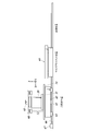
- FIG. 1 is an overall configuration diagram of an example of a patterning apparatus of the present invention (a diagram viewed from the X-axis direction).
- 1 is an overall configuration diagram of an example of a patterning apparatus of the present invention (a diagram viewed from the Y-axis direction).
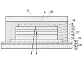
- Operation flow diagram of an example of patterning method of the present invention Cross-sectional view of an example of an organic EL element Schematic diagram of another example of light irradiation area
- the organic electroluminescent element patterning method of the present invention is a method for forming an organic electroluminescent element light-emitting pattern by irradiating an organic electroluminescent sheet provided with a plurality of organic electroluminescent elements through a mask.
- a region irradiated with light through the mask is divided into a plurality of light irradiation regions, and light is emitted from one light irradiation region (A) among the plurality of light irradiation regions.
- the additional light that irradiates the light irradiation region (A) in the first light irradiation step again.
- Morphism includes the step, accumulated light quantity of the plurality of light irradiation region, so that a predetermined amount of each of the light irradiation region, and a light irradiation process is repeated. This feature is a technical feature common to the claimed invention.
- the second light irradiation step is performed by irradiating the light irradiation region (B) other than the light irradiation region subjected to the light irradiation in the first light irradiation step with the light source unit.
- productivity is high and it is possible to prevent deterioration of the light emitting performance of the organic electroluminescence element and to perform more accurate patterning while suppressing thermal deformation of the mask.
- region is matched with either of the several light source parts for light irradiation, The position of the said several light source part, and the said organic electroluminescent sheet
- a patterning device for an organic electroluminescence element used in the present invention As a patterning device for an organic electroluminescence element used in the present invention, a pattern forming body mounting table for holding an organic electroluminescence sheet provided with a plurality of organic electroluminescence elements, and a plurality of light irradiations of the organic electroluminescence sheet At least one light source unit that irradiates the region with light, a step moving unit that changes a relative position between the position of the light source unit and the pattern forming object mounting table, and an integrated light amount in the plurality of light irradiation regions.
- a control unit that controls the light source unit so that a predetermined amount is obtained in each light irradiation region, and the step moving unit performs light irradiation in at least one light irradiation region (A) among the plurality of light irradiation regions. After performing, at least one light irradiation region (B) of the light irradiation regions other than the light irradiation region (A). After moving the light source unit or the pattern forming body mounting table to the position where light irradiation is performed in step, and performing light irradiation in the light irradiation region (B), the light source is moved to the position where light irradiation is performed again on the light irradiation region (A).
- the patterning device for an organic electroluminescence element is a step moving unit for moving the unit or the pattern forming body mounting table.
- productivity is high, deterioration of the light emitting performance of the organic electroluminescence element can be prevented, and more accurate patterning can be performed.
- a patterning device for the organic electroluminescence element used in the present invention a pattern forming body mounting table that holds an organic electroluminescence sheet provided with a plurality of organic electroluminescence elements, and a plurality of organic electroluminescence sheets
- a patterning device for an organic electroluminescence sheet comprising a plurality of light source units for irradiating light to a light irradiation region and a control unit for controlling the plurality of light source units, wherein the positions of the plurality of light source units are fixed
- the plurality of light irradiation regions are associated with one of the plurality of light source units, and the control unit controls the plurality of light source units to correspond to at least one light irradiation region (A).
- the light irradiation region (A) After performing light irradiation in the light irradiation region (A) by the light irradiation unit, the light irradiation region (A) Light irradiation was performed in the light irradiation region (B) by the light source unit corresponding to at least one light irradiation region (B) in the outside light irradiation region, and light irradiation was performed in the light irradiation region (B). Later, the light irradiation area (A) is again irradiated with light, and the patterning of the organic electroluminescence element that controls the light source unit so that the accumulated light quantity in the plurality of light irradiation areas becomes a predetermined amount in each light irradiation area. An apparatus is preferred. Thereby, productivity is high, and while the deterioration of the light emission performance of an organic electroluminescent element can be prevented, more accurate patterning can be performed.
- ⁇ is used to mean that the numerical values described before and after it are included as a lower limit value and an upper limit value.
- the patterning method of the present invention is a method for patterning an organic electroluminescent element in which a light emitting pattern of an organic electroluminescent element is formed by irradiating an organic electroluminescent sheet provided with a plurality of organic electroluminescent elements through a mask.
- the region irradiated with light through the mask is divided into a plurality of light irradiation regions, and light irradiation is performed in one light irradiation region (A) among the plurality of light irradiation regions.
- the light irradiation region (A) of the first light irradiation step includes an additional light irradiation step of performing light irradiation again, and the plurality of light irradiation regions Definitive total irradiation quantity of light, to a predetermined amount in each of the light irradiation region, and a light irradiation process is repeated.
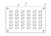
- FIG. 1A and 1B are schematic views of an organic EL sheet and a mask.
- FIG. 1A is a schematic diagram of an organic EL sheet.
- a plurality of organic EL elements 12 are formed on the organic EL sheet 11, and organic EL alignment marks 13 are formed at the four corners. This alignment mark is used for alignment of a film formation mask when forming an electrode or an organic layer in the manufacture of an organic EL element.
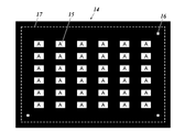
- FIG. 1B is a schematic diagram of a mask.
- a predetermined light irradiation pattern 15 (character A in the example in the figure) is formed on the mask 14 at a position corresponding to each organic EL element, and a mask alignment mark 16 corresponding to the position of the alignment mark 13 on the organic EL sheet 11. Is formed.
- the blackened portion shields the ultraviolet rays by the light shielding film. Therefore, the organic EL element is irradiated with ultraviolet light in a light emitting area other than the letter A and does not emit light, and only the letter A emits light as the organic EL element.
- the mask substrate is preferably quartz glass or heat-resistant glass (Pyrex (registered trademark) or Tempax) having a small linear expansion coefficient
- the light-shielding film is preferably a chromium film or a chromium oxide film having a low ultraviolet absorption rate.
- the organic EL sheet 11 is cut for each organic EL element 12.
- Each individual organic EL element thus cut is used to be individually loaded into a display device or the like.
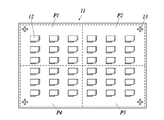
- FIG. 2 is a schematic diagram showing a light irradiation region.
- the dotted line portion in the figure is a plurality of light irradiation regions, and in the case of FIG. 2, the case where it is divided into four light irradiation regions (P1 to P4) is illustrated.
- the tact time in the case where the four light irradiation areas are irradiated 10 times with one pulse light irradiation is illustrated.
- 1 pulse light irradiation irradiance 4 ⁇ 10 4 W / m 2
- is irradiated for 30 seconds light amount 1.2 ⁇ 10 6 J / m 2
- One pulse light irradiation is applied for 30 seconds.
- each of the light irradiation regions P3 and P4 is also irradiated with one pulse of light for 30 seconds.
- one-pulse irradiation is sequentially repeated.
- the light irradiation is repeated 10 times until the integrated light quantity at each position becomes 1.2 ⁇ 10 7 J / m 2 (circumferential light irradiation method).
- There is a waiting time of 94 seconds before returning to the light irradiation region P1 and since the light irradiation region P1 is sufficiently cooled during this time, heat accumulation in the mask and the organic EL sheet does not occur during light irradiation. .
- the tact time required to complete the light irradiation is (light irradiation 30 seconds + step movement 1 second) ⁇ 4 steps ⁇ 10 times, which is 1240 seconds.
- the tact time in the case where the four light irradiation regions are completed by one round of multipulse light irradiation (intermittent light irradiation) (when the present invention is not used) is exemplified.
- one pulse light irradiation (irradiance 4 ⁇ 10 4 W / m 2 ) is irradiated for 30 seconds (light amount 1.2 ⁇ 10 6 J / m 2 ) and then turned off for 30 seconds.
- This intermittent light irradiation is repeated 10 times, and light irradiation is performed until the integrated light amount becomes 1.2 ⁇ 10 7 J / m 2 .
- the light irradiation region P2 is moved in 1 second and the same light irradiation is performed.
- the same light irradiation is performed for the light irradiation region P3 and the light irradiation region P4.
- the tact time is (irradiation 30 hours seconds + light-off time 30 seconds) ⁇ 10 times ⁇ 4 positions + step movement 1 second ⁇ 3 steps, 2403 seconds.
- the tact time can be reduced to almost half of the comparative intermittent light irradiation.
- the light irradiation area in the present invention is divided into a plurality of parts.
- the number of light irradiation regions to be divided is not particularly limited, but is preferably 9 or less, and more preferably 4 or less from the viewpoint of shortening the tact time. More preferably, it is divided into two.
- a repetition order of the light irradiation region for example, a case where (light irradiation region P1 ⁇ light irradiation region P2 ⁇ light irradiation region P1 ⁇ light irradiation region P2) is repeated may be mentioned, but re-lighting is performed in at least one light irradiation region. As long as irradiation is performed, any light irradiation order may be sufficient.
- the light irradiation order may be different from the light irradiation order of the first round.
- the shape of the light irradiation region to be divided may be any of square, rectangle and the like.
- the irradiance and the light irradiation time of one pulse may be changed at each position.
- one pattern may be formed with a plurality of organic EL elements (for example, 100 organic EL elements in a total of 10 rows and 10 rows).
- the plurality of organic EL elements form different patterns, and operate as an organic EL panel that displays one pattern as a whole.
- a pattern forming body mounting table for holding an organic electroluminescence sheet provided with a plurality of organic electroluminescence elements, and a plurality of light irradiation regions of the organic electroluminescence sheet
- At least one light source unit that performs light irradiation
- a step moving unit that changes a relative position between the position of the light source unit and the pattern forming body mounting table, and an integrated light amount in each of the plurality of light irradiation regions
- a control unit that controls the light source unit so that a predetermined amount is obtained in the light irradiation region, and the step moving unit performs light irradiation in at least one light irradiation region (A) among the plurality of light irradiation regions.
- At least one light irradiation region (B) other than the light irradiation region (A) is irradiated with light.
- the light source part or the pattern forming body mounting table is moved to the light irradiation area (B), and then the light irradiation area (A) is irradiated with light again.
- a patterning device for an organic electroluminescence element which is a step moving unit for moving the mounting table is preferable.
- FIG. 3 is a perspective view of an example (first embodiment) of the light irradiation unit of the patterning apparatus of the present invention. *
- a light source section 35 for example, a UV-LED having a wavelength of 365 nm or 385 nm
- the heat of the LED generated at the time of irradiation escapes to the heat radiating plate 33 and prevents the light emission efficiency of the LED from being lowered. It is more preferable to provide a cooling pipe inside the heat radiating plate 33 and circulate cooling water to cool the LED with water.
- the divergent light emitted from the light source unit 35 is used as irradiation light 38 shaped into a light beam having a predetermined divergence angle by the lens array 37.
- Irradiation light 38 is confined by a cover 39 whose inner surface is a reflective surface to prevent a decrease in the amount of light, and the organic EL sheet 11 is irradiated with light through the mask 14 with a uniform amount of light.
- the gap WD between the lower end of the cover and the mask should be as narrow as possible, preferably about 5 mm. If it is this space
- the light emitted from the light source unit 35 is preferably ultraviolet light whose deactivation reaction rate of the organic functional layer is fast from the viewpoint of reducing the tact time.
- the light irradiation performed in one light irradiation step is preferably pulsed light irradiation. Furthermore, it is more preferable that it is 1 pulse light irradiation.
- the intermittent time (total of light extinction time) between one light irradiation steps, It is preferably 25% or less, more preferably 10% or less, of the time required for the single light irradiation step. Most preferably, the intermittent time is 0%.
- the light source unit 35 (LED) is irradiated with light by being controlled by the light source control unit 56 to be turned on / off or irradiated and turned on.
- the lens array 37 is used for divergence angle shaping, a condensing mirror such as a compound parabolic concentrator may be used.
- the organic EL sheet 11 is placed on the pattern forming body placing table 43, and the mask 14 is adjusted to a predetermined relative position with the organic EL sheet 11 and placed on the sheet.
- the organic EL sheet 11 is preferably fixed by adsorption.
- PET or PEN is used for the substrate, the organic EL sheet is easily deformed, such as curling, but by adsorbing the entire surface of the sheet, it can be fixed to the pattern forming object mounting table with good flatness and prevent light irradiation blur of patterning it can.
- the pattern forming body mounting table 43 cools the organic EL sheet by a water cooling method. Cooling pipes 44a and 44b are provided inside the pattern forming body mounting table to cool the heat generated in the mask and the organic EL sheet by ultraviolet irradiation.
- the water that has absorbed the heat in the pattern forming body mounting table is sent to a chiller unit 58 installed outside (not shown), heat is exchanged inside the chiller unit, and the cooling water whose temperature is lowered is supplied to the pattern forming body mounting table. Supplied.
- the cooling water circulates through the chiller unit and the pattern forming body mounting table. The cooling function is always operated while the device is in operation.
- the water temperature introduced into the pattern forming body mounting table is preferably 30 ° C. or less as long as the organic EL sheet and the mask do not condense. 10 to 20 ° C. is more preferable.
- the material of the pattern forming body mounting table is preferably a metal having high thermal conductivity. For example, aluminum can be used.
- Gas is blown out from the gas flow generation unit 40 in a line shape, and the gas flow 41 cools the mask surface.
- the gas blown by the gas flow generating part is not particularly limited as long as it can cool the mask and does not impair the effects of the present invention.
- air or nitrogen gas can be suitably used.
- the glass mask 14 irradiated with ultraviolet rays becomes high temperature and thermally expands, and patterning with high dimensional accuracy is likely to be difficult. Moreover, the organic EL sheet 11 is heated, and the light emission performance of the organic EL element is likely to be deteriorated.
- the light irradiation area of the organic EL sheet is divided into a plurality of light irradiation areas to reduce the light irradiation area, thereby suppressing the heat generation amount of the mask and sequentially performing the light irradiation, and then the same again.
- the productivity is high, the deterioration of the light emitting performance of the organic electroluminescence element is prevented, and accurate patterning can be performed.
- the light irradiation unit 32 irradiates the first light irradiation region P ⁇ b> 1 of the organic EL sheet 11
- the light irradiation unit 32 and the pattern forming body mounting table 43 move stepwise.
- the next light irradiation region P2 is irradiated with light.
- the light irradiation region P1 is again irradiated with light.
- the glass mask 14 is prevented from being deformed by heat and the color balance of the organic EL sheet 11 is prevented from being accurately patterned. Further, the time tact for patterning can be shortened, and productivity can be improved.
- a patterning apparatus used in the patterning method of the present invention, a pattern forming body mounting table for holding an organic electroluminescence sheet provided with a plurality of organic electroluminescence elements, and a plurality of light irradiation regions of the organic electroluminescence sheet
- a patterning device for an organic electroluminescence sheet comprising a plurality of light source units for irradiating light and a control unit for controlling the plurality of light source units, wherein the positions of the plurality of light source units are fixed,
- the light irradiation region is associated with one of the plurality of light source units, and the control unit controls the plurality of light source units by the light irradiation unit corresponding to at least one light irradiation region (A).
- the light source corresponding to at least one light irradiation region (B) is irradiated with light in the light irradiation region (B), and after the light irradiation is performed in the light irradiation region (B), the light irradiation region (A
- the light source unit is controlled so that the integrated light quantity in the plurality of light irradiation regions becomes a predetermined amount in each light irradiation region. Preferably there is.
- FIG. 4 is a perspective view of another example (second embodiment) of the light irradiation unit of the patterning apparatus of the present invention.
- a plurality of light source sections 35 are arranged, and the light irradiation area of the light emitted from the entire light irradiation section 32 is an area that can cover the entire area where the organic EL element of the sheet is disposed. . That is, when all the light source parts 35 are turned on, the light irradiation area covers all the light irradiation areas P1, P2, P3 and P4 in FIG.
- the light source unit 35 can be controlled for each group, and in the first light irradiation step, only the LED light source unit of the first group is turned on, and the irradiation light 1 (38a) that irradiates the light irradiation region P1 in FIG. ) Is emitted.
- irradiation light 2 (38b) for irradiating the light irradiation region P2 in FIG. 2 is emitted.
- irradiation light 2 (38b) for irradiating the light irradiation region P2 in FIG. 2 is emitted.
- the light source unit 35 in one light irradiation unit 32 is sequentially turned on.
- a plurality of (for example, four) light irradiation units 32 in the first embodiment of the patterning device described above are arranged, and each light Each light irradiation unit 32 may be caused to emit light sequentially in accordance with the light irradiation of the irradiation regions (P1 to P4).
- the gas flow generating unit 40 is arranged at a position facing the upper surface of the glass mask 14 such that gas is blown in parallel to the glass mask 3 and toward the center of the glass mask 14 through the gap WD between the glass mask 14 and the cover 39. Has been.
- the gas flow generating unit 40 is disposed on the upper surface of the glass mask 14 and sprayed in parallel with the glass mask 14, whereby the gas flow 41 to be sprayed travels on the glass mask 14 evenly and joins at the center of the glass mask.
- To spray in parallel means to spray at an angle within ⁇ 2 degrees with respect to the plane of the glass mask 3.
- the gas flow generation unit 40 is disposed in parallel to the opposing position on the upper surface of the glass mask 14.
- the distance 42 between the cover 39 and the gas flow generating unit 40 is not particularly limited as long as air is efficiently blown onto the mask, but is preferably within a range of 10 to 200 mm. More preferably, it is within the range of 30 to 100 mm.
- the length of the gas flow generating part is preferably the same as or larger than the width of the cover on the side to be sprayed.
- the pair of gas flow generation units 40 is disposed at a symmetrical position with respect to the central portion of the glass mask 14.
- cooling pattern pipes 44a and 44b are provided inside the pattern forming body mounting table 43, and a chiller unit 58 that cools the organic EL sheet and the mask by circulating cooling water through the cooling pipe is preferably provided.
- the gas flow generation unit 40 is preferably provided with a slit-shaped or nozzle-shaped sprayed portion. It is more preferable to have a slit-shaped spraying part.
- the number of nozzles is preferably large, and the number of nozzles is preferably one at intervals of 5 to 20 mm.
- the size of the nozzle diameter can be adjusted as appropriate.
- a commercially available product can be used as the slit-shaped spraying part used for the spraying part.
- a layered airflow generator 750 type manufactured by Sanwa Enterprise, a blower knife air nozzle manufactured by Spraying System Japan, or the like can be used.
- the air volume blown from the pair of blowing parts is the same.
- the air volume can be 1000 to 4000 L / min.
- the gas flow generator is preferably connected to an air compressor. According to the irradiation light quantity of an ultraviolet-ray, it can adjust to a desired air volume and a wind speed suitably.
- a known air compressor can be used.
- the air to be blown is temperature-adjusted. If necessary, the cooling efficiency can be increased by using air whose temperature is adjusted to about 5 to 15 ° C., for example.
- the cover has a reflection light guiding function that prevents a reduction in the amount of ultraviolet light emitted from the lens array and irradiates the glass mask with a uniform amount of light. Therefore, it is preferable that the inner surface is covered with a reflective material. Since the reflective material is resistant to heat and durable, a metal material can be used. For example, aluminum is preferably used because it is lightweight.
- the height and bottom area are not particularly limited, and the organic EL sheet irradiates ultraviolet rays. It can be set according to the size of.
- the bottom surface is preferably larger than the area where the organic EL elements are arranged.
- the height of the cover can be adjusted as appropriate based on the amount of ultraviolet light and unevenness in the amount of irradiation light. For example, it can be about 0.5 to 5 m.
- a light source that emits ultraviolet rays is attached to the light source unit.
- the light source is not particularly limited as long as it is a light source that emits a desired amount of ultraviolet light.
- Ultraviolet light having a wavelength range of 400 nm can be used. It is desirable to use a UV-LED that can easily control pulse irradiation electrically and can increase the output of the light source.
- One or a plurality of light sources may be used for the light source unit, but it is preferable to arrange a plurality of light sources in a two-dimensional manner to form one light source unit.
- the integrated light irradiation amount for performing the patterning method of the present invention is 2 ⁇ 10 6 to 5 ⁇ 10 7 J / m 2 , although it depends on the layer structure, film thickness, panel size, etc. of the organic EL element. Irradiation with a light amount is preferable from the viewpoint of high productivity and accurate patterning with good contrast between the light emitting portion and the non-light emitting portion. Further, it is preferable that one pulse of ultraviolet irradiation time is in the range of 1 to 300 seconds.
- a mask has a role which changes the light quantity irradiated to an organic EL element.
- a glass mask having a negative pattern on a glass substrate can be manufactured using a known mask material that can change the amount of transmitted ultraviolet light. By irradiating the organic EL element with ultraviolet rays through this mask, an organic EL element having a light emission pattern can be produced.
- a photographic image can be produced by using a black and white photographic negative image in which silver fine particles are dispersed in a gelatin film.
- the “pattern” here means a design (design or pattern of a figure), characters, images, etc. displayed by the organic EL element. “Patterning” refers to providing these pattern display functions.
- the “light emission pattern” refers to light emitted from an organic EL element that emits light with varying light emission intensity (luminance) depending on the position of the light emitting surface, based on a predetermined design (pattern or pattern in the figure), characters, images, etc.
- the glass substrate is not particularly limited as a material, and for example, a known glass material used for optics or a substrate can be used.
- glass ceramics such as aluminosilicate glass, soda lime glass, soda aluminosilicate glass, aluminoborosilicate glass, borosilicate glass, quartz glass, chain silicate glass, crystallized glass, heat-resistant glass, phosphate glass or Examples thereof include lanthanum-based glass.
- Quartz glass and heat-resistant glass can be preferably used.
- the thickness of the glass mask is not particularly limited, but a glass mask having a thickness of 3 to 10 mm can be used.
- ⁇ Chiller> In addition to cooling with the gas blown from the gas flow generation unit, it is preferable to cool the organic EL sheet and the mask by providing the pattern forming body mounting table with a cooling function. Since the organic EL sheet is as thin as 0.1 to 0.5 mm, the heat generated in the light shielding film of the mask due to ultraviolet irradiation is also cooled through the organic EL sheet. As a cooling method, a known method can be mentioned, but a water cooling method is preferable because it is simple and effective. A cooling pipe is provided inside the pattern forming body mounting table, and cooling water flows through the cooling pipe and absorbs heat generated in the mask and the organic EL sheet by ultraviolet irradiation.
- the cooling water that has absorbed heat by the pattern forming body mounting table is sent to the chiller unit installed outside, heat is exchanged inside the chiller unit, and the cooling water whose temperature is lowered is supplied to the pattern forming body mounting table.
- the cooling water circulates through the chiller unit and the pattern forming body mounting table.
- the “chiller” refers to a device that circulates a heat medium and keeps the target part at a constant temperature.
- the chiller unit has a built-in cooler for heat exchange and a pump for circulating cooling water.
- FIG. 3 and FIG. 4 show an example in which the cooling pipes 44a and 44b provided on the pattern forming body mounting table 43 flow circulating water. Cooling water is introduced through the cooling pipe (introduction) 44a and discharged from the cooling pipe (discharge) 44b, and the discharged water is cooled again and circulated to cool the organic EL sheet 11 and the mask 14 irradiated with ultraviolet rays. be able to.
- the material of the pattern forming body mounting table preferably has a high thermal conductivity.
- aluminum can be used.
- ⁇ Circular light irradiation mechanism> In the present invention, after the light irradiation area of the organic EL sheet is divided into a plurality of light irradiation areas and sequentially irradiated with light, the same area is repeatedly irradiated with light again, and a predetermined integrated light irradiation amount is obtained in each light irradiation area. Repeat the light irradiation until Therefore, it is necessary to control the light irradiation area so as to go around.
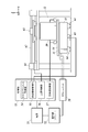
- FIG. 5 is an overall configuration diagram (a diagram viewed from the X-axis direction) of an example of the patterning device of the present invention (a first mode of the patterning device).
- FIG. 6 is an overall configuration diagram (a diagram viewed from the Y-axis direction) of an example of the patterning device of the present invention (a first embodiment of the patterning device).
- the pattern forming body mounting table 43 moves along the linear guide 64 in the X-axis direction.
- the screw shaft 66 is rotated by the motor 67, and the rotational movement is converted into the straight movement by the ball screw 65 attached to the bottom surface of the pattern forming object mounting table 43, and moved.
- the reference position is determined by a position sensor (not shown), and the movement amount is controlled by the number of rotations of the motor 67 from there.
- the light irradiation unit 32 is similarly moved in the Y-axis direction by the linear guide 68.
- the linear guide 68 of the light irradiation unit is installed on a base on which a support is placed.
- the operation unit 52 has a built-in memory, and stores light irradiation conditions such as irradiance per light irradiation at each position, light irradiation time, number of times of light irradiation, coordinates of each light irradiation position, and movement order. ing.
- the desired light irradiation conditions are selected by the operation unit 52, and the control unit 53 controls the following mechanisms according to the conditions.
- the control unit 53 includes a mask alignment control unit 54, a movement mechanism control unit 55, a light source control unit 56, and an air flow control unit 57.
- the light source control unit 56 controls the irradiance, light irradiation time, the number of times of light irradiation, etc. of the light source unit 35.
- the movement mechanism control unit 55 controls the positions of the pattern forming body mounting table 43 and the light irradiation unit 32 via the motor 67 and the motor 61.
- the mask alignment control unit 54 controls the mask alignment device 69 in a state where the pattern forming object mounting table 43 is at the mask alignment position, and places the mask 14 at a predetermined position on the organic EL sheet 11.
- the air flow control unit 57 controls on / off of the operation of the air flow generation unit 40.
- FIG. 7 is a flowchart showing an operation flow of an example of the patterning method of the present invention (when the first embodiment of the patterning apparatus is used and there are four light irradiation regions).
- step S101 light irradiation conditions are selected. Light irradiation conditions are selected using a touch panel (not shown) of the operation unit 52. Further, the ID number of the organic EL sheet 13 is input. Next, the process proceeds to step S102.
- step S ⁇ b> 102 the organic EL sheet 11 is set on the pattern forming body mounting table 43.
- the pattern forming body mounting table 43 is in a position retracted from the light source unit, and the organic EL sheet 11 is installed and collected at this position.
- a suction start button is pressed on a touch panel (not shown) of the operation unit 52, and the organic EL sheet 11 is sucked and fixed in a suction hole (not shown) provided on the pattern forming body mounting table 43.
- the process proceeds to step S103.
- step S103 mask alignment is performed, and the mask 14 is placed at a predetermined position of the organic EL sheet 11.
- a light irradiation start button is pressed on a touch panel (not shown) of the operation unit 52, the pattern forming body mounting table 43 on which the organic EL sheet 11 is mounted moves to the mask alignment position.
- Mask alignment is performed by the mask alignment apparatus 69, and the mask 14 is placed in close contact with the organic EL sheet 11.
- the process proceeds to step S104.
- step S104 circular step light irradiation is performed.
- the pattern forming body mounting table 43 When the circular step light irradiation is started, the pattern forming body mounting table 43 first moves to the light irradiation position.
- the moving mechanism control unit 55 moves the pattern forming body mounting table 43 through the ball screw 65 so as to be a predetermined place in the light irradiation region P1.
- the gas flow control unit 57 operates the gas flow generation unit 40 to start air cooling.
- the moving mechanism control unit 55 moves the light irradiation unit 32 through the ball screw 63 so that the light irradiation region P1 is at a predetermined place.
- the light source control unit 56 operates the light source unit 35 to perform predetermined one-pulse light irradiation.
- the moving mechanism control unit 55 moves the pattern forming body mounting table 43 through the ball screw 65 so as to be a predetermined place in the light irradiation region P2.
- the light source control unit 56 operates the light source unit 35 to perform predetermined one-pulse light irradiation.
- the moving mechanism control unit 55 moves the light irradiation unit 32 through the ball screw 63 so that the light irradiation unit 32 is located at a predetermined position in the light irradiation region P3.
- the light source control unit 56 operates the light source unit 35 to perform predetermined one-pulse light irradiation.
- the moving mechanism control unit 55 moves the pattern forming body mounting table 43 through the ball screw 65 so as to be a predetermined place in the light irradiation region P4.
- the light source control unit 56 operates the light source unit 35 to perform predetermined one-pulse light irradiation.
- the control unit 53 determines whether a predetermined number of times of light irradiation has been performed. If the predetermined number of times of light irradiation has not been performed, the light irradiation region P1 is moved and light irradiation is repeated.
- step S105 the air control unit 57 stops the operation of the gas flow generation unit 40 and stops air cooling.
- step S106 the process proceeds to step S106.
- step S106 the pattern forming body mounting table 43 moves to the mask alignment position. Next, the process proceeds to step S107.
- step S107 the mask 14 is separated from the organic EL sheet. Next, the process proceeds to step S108.
- step S108 the pattern forming body mounting table 43 moves to the retracted position.
- step S109 the process proceeds to step S109.
- step S109 the adsorption of the pattern forming body mounting table 43 is stopped, and the organic EL sheet is collected.
- the step movement of the circulating light irradiation can be performed immediately by controlling the light emission switching of the light source group in the plurality of light source units (LEDs) 35 by the light source control unit 56. .
- the tact time can be shortened by the time of step movement.
- Other processes can be performed in the same manner as in the second embodiment.
- the organic EL device includes one or a plurality of organic functional layers between at least a pair of electrodes.
- the organic functional layer in the present invention refers to a layer containing an organic compound. Examples thereof include a hole injection layer, a hole transport layer, a light emitting layer (including a blue light emitting layer, a green light emitting layer, and a red light emitting layer), an electron transport layer, and an electron injection layer.
- the organic EL element according to the present invention can take various configurations, and an example is shown in FIG. In FIG. 8, the aspect ratio is not accurate for explanation.
- an organic functional layer unit (117) having a light emitting layer and a second electrode (118) serving as a cathode are laminated on a first electrode (116) serving as an anode. Furthermore, the gas barrier film (101), the sealing resin layer (119), and the sealing member (120) are solid-sealed.
- the 1st electrode (116) used as an anode is comprised as a translucent electrode. In such a configuration, only a portion where the organic functional layer unit (117) is sandwiched between the first electrode (116) and the second electrode (118) is a light emitting region in the organic EL element (101).
- the organic EL element (12) is configured as a bottom emission type in which generated light (hereinafter referred to as emitted light (h)) is extracted from at least the gas barrier film (101) side. ing.
- the organic EL element (12) includes a sealing resin layer (119) covering the first electrode (116), the organic functional layer unit (117), and the second electrode (118) on one surface of the gas barrier film (101). ) Through which the sealing member (120) is bonded.
- the solid-sealed organic EL element (12) is attached to the bonding surface of the sealing member (120) or the gas barrier layer (104) and the second electrode (118) of the gas barrier film (101).
- An uncured resin material is applied, and the gas barrier film (101) and the sealing member (120) are integrated by thermocompression bonding with the resin material interposed therebetween.
- the organic EL device (12) according to the present invention is not limited to the bottom emission type, but is a top emission type configuration in which light is extracted from the second electrode (118) side, or a dual emission type in which light is extracted from both sides. It is good also as a structure. If the organic EL element (12) is a top emission type, a transparent material is used for the second electrode (118), and the emitted light h is extracted from the second electrode (118) side. Further, when the organic EL element (12) is a double-sided light emitting type, a transparent material is used for the second electrode (118), and the emitted light h is extracted from both sides.
- a hard coat and a gas barrier layer were formed on the surface of the prepared triacetyl cellulose film to obtain a base film.
- an organic EL element 12A was produced according to the following method using the produced base film.
- the base film was fixed to a base holder of a commercially available vacuum deposition apparatus, and the following compound No. 10 was put in a resistance heating boat made of tungsten, and the base film holder and the heating boat were mounted in the first vacuum chamber of the vacuum deposition apparatus. Moreover, silver (Ag) was put into the resistance heating boat made from tungsten, and it attached in the 2nd vacuum chamber of a vacuum evaporation system.
- a heating boat containing 10 was energized and heated, and the base layer of the first electrode was provided with a layer thickness of 10 nm at a deposition rate of 0.1 to 0.2 nm / second.
- the base film on which the underlayer was formed was transferred to the second vacuum chamber while maintaining a vacuum, and after the pressure in the second vacuum chamber was reduced to 4 ⁇ 10 ⁇ 4 Pa, the heating boat containing silver was energized and heated.
- a first electrode made of silver having a thickness of 8 nm was formed at a deposition rate of 0.1 to 0.2 nm / second.
- the following compound HT-1 was deposited on the formed first electrode while moving the base film, with a deposition rate of 0 Evaporation was performed at a rate of 1 nm / second, and a 20 nm hole transport layer (HTL) was provided.
- the following compound A-3 blue light emitting dopant
- the following compound A-1 green light emitting dopant
- the following compound A-2 red light emitting dopant
- the following compound H-1 host compound
- -3 changes the deposition rate so that the content is linear with respect to the layer thickness direction and the gradient is 35% to 5%, and the compound A-1 and the compound A-2 do not depend on the layer thickness.
- the compound H-1 has a gradient concentration of 64.6% to 94.6% in the layer thickness direction so that each concentration is constant at 0.2% by mass.
- the vapor deposition rate was changed so that a co-deposited light emitting layer having a layer thickness of 70 nm was formed.
- the following compound ET-1 was deposited on the light emitting layer to form an electron transport layer having a thickness of 30 nm, and potassium fluoride (KF) was further deposited to form an electron injection layer having a thickness of 2 nm. Furthermore, aluminum was vapor-deposited to form a second electrode having a layer thickness of 110 nm.
- KF potassium fluoride
- thermosetting sheet adhesive epoxy resin
- a sealing resin layer on one surface of the aluminum foil with a thickness of 20 ⁇ m.
- the resin base material prepared up to the second electrode was superposed.
- the adhesive forming surface of the sealing member and the organic functional layer surface of the element were continuously overlapped so that the ends of the lead wires of the first electrode and the second electrode were exposed.
- the sample including the gas barrier film was placed in a decompression device, and kept under a reduced pressure condition of 90 ° C. and 0.1 MPa for 5 minutes while applying pressure to the stacked sample and the sealing member. Subsequently, the sample including the gas barrier film was returned to the atmospheric pressure environment and further heated at 120 ° C. for 30 minutes to cure the adhesive.
- the sealing process is performed under atmospheric pressure and in a nitrogen atmosphere with a moisture content of 1 ppm or less in accordance with JIS B 9920.
- the measured cleanliness is class 100, the dew point temperature is ⁇ 80 ° C. or less, and the oxygen concentration is 0.8 ppm or less. At atmospheric pressure.
- an organic EL element 12A was produced.
- the size of one organic EL element was 60 mm ⁇ 150 mm.
- the organic EL elements 12A were arranged in 6 rows and 6 rows, and a total of 36 organic EL elements were prepared to obtain an organic EL sheet 11A.
- the size of the organic EL sheet 11A was 610 mm ⁇ 11500 mm.
- One time of light irradiation was irradiation with 1 pulse light, and irradiation with irradiance of 4 ⁇ 10 4 W / m 2 was performed for 30 seconds to obtain a light amount of 1.2 ⁇ 10 6 J / m 2 .
- the integrated light quantity in one region was set to 1.2 ⁇ 10 7 J / m 2 .
- Other patterning conditions are shown below.
- ⁇ Glass mask> After patterning the pattern shown in FIG. 1B by laser drawing on a resist applied to a glass substrate (quartz glass) having a thickness of 5 mm and a size of 850 ⁇ 1400 mm and having a chromium film formed on the entire surface, etching is performed. Then, an unnecessary chromium film was removed, and a glass mask on which the chromium film having the pattern was formed was used.
- the organic EL sheet 11A was adsorbed and fixed on the pattern forming body mounting table with the light emitting surface facing up, and a glass mask was placed in close contact with the organic EL sheet 11A at a predetermined position.
- Light source LED irradiation area with a wavelength of 385 nm: 290 mm ⁇ 560 mm ⁇ Gas flow generator>
- the spray part sprayed with the same air volume from the direction of both short sides to the center direction of the glass mask using the slit-like layered gas flow generation part. Air was used as the gas.
- Slit position of spraying part 3mm above glass
- Angle of sprayed part of gas flow generating part parallel to glass mask (0 degree)
- a pair of gas flow generation portions was attached at a position facing the short side of the cover with a gap of 8:40 mm between the gas flow generation portion and the cover side surface.
- Air temperature 25 ° C
- Compressed air pressure 0.2 MPa
- Air consumption 1000L / min ⁇ Chiller>
- a cooling pipe having a diameter of 18 mm was provided inside the pattern-formed body mounting table made of aluminum, and cooling water having a temperature of 20 ° C. was circulated at a flow rate of 9 L / min.
- the organic EL sheet patterned in this manner was used as an organic EL sheet 11B (present invention), which was cut into a total of 36 organic EL elements in 6 rows and 6 rows. Using this one organic EL element, an organic EL display device was obtained, and the display performance was visually evaluated.
- the total tact time required for the patterning light irradiation step was 1240 seconds. Further, the color of the light emitting portion patterned into the letter A was not deviated from white, and the heel border line was emitted without any disturbance in shape. Further, the width of the luminance distribution in the region where the luminance decreases from the light emitting portion to the non-light emitting portion at the boundary line was obtained with edges of 80 ⁇ m and less than 100 ⁇ m, and it was possible to pattern clearly. Furthermore, the ratio of the luminance of the light emitting part to the luminance of the non-light emitting part was 67, which was a high contrast with respect to the target of 50 or more.
- Example 2 ⁇ Preparation of Organic EL Sheet 11C (Comparative Example)>
- an organic EL sheet 11C was produced in the same manner as in Example 1 except that the light irradiation conditions were changed as follows.
- the circular pattern of the light irradiation was performed once (light irradiation region P1 ⁇ light irradiation region P2 ⁇ light irradiation region P3 ⁇ light irradiation region P4).
- the light irradiation of one region was multi-pulse light irradiation in which pulse light irradiation with irradiation time of 20 seconds was repeated 10 times after irradiation with irradiance 4 ⁇ 10 4 W / m 2 for 30 seconds.
- the integrated light quantity was set to 1.2 ⁇ 10 7 J / m 2 .
- the turn-off time was set to 20 seconds.
- the total tact time required for the patterning light irradiation process was 2003 seconds.
- the organic EL element disposed near the center of the sheet obtained a light emission pattern equivalent to the patterning result of the organic EL sheet 11B, but the organic EL element disposed in the corner portion of the sheet has a target luminance ratio of 54.
- the luminance distribution width at the pattern boundary in a specific direction was as large as 190 ⁇ m. This was caused by warping of the mask due to heat storage by multipulse light irradiation, and a gap was generated between the mask and the organic EL sheet at the corner of the mask.
- Example 3 ⁇ Preparation of organic EL sheet 11D (present invention)>
- an organic EL sheet 11D was produced in the same manner as in Example 1 except that the light irradiation device was changed to the light irradiation device (second form) shown in FIG. .
- the irradiation area is 580 mm ⁇ 1120 mm.
- the total tact time required for the patterning light irradiation process was 1236 seconds.
- Example 4 ⁇ Production of Organic EL Sheet 11E (Invention)>
- an organic EL sheet 11D was produced in the same manner as in Example 1 except that the light irradiation region was changed to two regions (P1 and P2) shown in FIG.
- the total tact time required for the patterning light irradiation process was 620 seconds.
- the patterning method and patterning device of the present invention are highly productive, prevent deterioration of the light emitting performance of the organic electroluminescent element, and can perform accurate patterning by suppressing thermal deformation of the mask, thereby patterning the organic electroluminescent element. It can be used for various displays used as a panel.
Landscapes
- Engineering & Computer Science (AREA)
- Manufacturing & Machinery (AREA)
- Electroluminescent Light Sources (AREA)
Abstract
本発明の課題は、生産性が高く、マスクの熱変形を抑制して正確なパターニングが可能な有機EL素子のパターニング方法を提供することである。 当該有機エレクトロルミネッセンス素子のパターニング方法は、マスクを介して光照射することにより、有機エレクトロルミネッセンス素子の発光パターンを形成する有機エレクトロルミネッセンス素子のパターニング方法であって、前記マスクを介して光照射する領域が、複数の光照射領域に区分されており、前記複数の光照射領域のうち、一つの光照射領域(A)で光照射を行う第1光照射工程と、前記光照射領域(A)以外の光照射領域のうちの一つの光照射領域(B)で光照射を行う第2光照射工程と、前記第1光照射工程の光照射領域(A)に再度光照射を行う追加光照射工程を含み、積算照射光量が、それぞれの光照射領域で所定量となるように、光照射工程が繰り返されることを特徴とする。
Description
本発明は、有機エレクトロルミネッセンス素子のパターニング方法及びパターニング装置に関する。より詳しくは、生産性が高く、有機エレクトロルミネッセンス素子の発光性能劣化を防止すると共に、正確なパターニングが可能な有機エレクトロルミネッセンス素子のパターニング方法及びパターニング装置に関する。
現在、薄型の発光デバイスとして有機発光パネルが注目されている。例えば、有機材料のエレクトロルミネッセンス(Electro Luminescence:EL)を利用した有機エレクトルルミネッセンス素子(以下「有機EL素子」ともいう。)は、数V~数十V程度の低電圧で発光が可能な薄膜型の完全固体パネルであり、低電力で高い輝度を得ることができ、視認性、応答速度、寿命、消費電力の点で優れ、薄型、軽量にできるといった多くの優れた特徴を有している。このため、有機EL素子をパネルとして用いた各種ディスプレイや、そのバックライト、看板や非常灯等の表示板、照明光源等の面発光体が近年注目されている。
このような有機ELパネルは、2枚の電極間に有機材料からなる発光層が配置された構成を有し、発光層で生じた発光光は電極を透過して外部に取り出される。このため、2枚の電極のうちの少なくとも一方は透明電極として構成され、透明電極側から発光光が取り出される。
有機ELパネルをディスプレイ用途に用いるため、パターニングされた有機EL素子を製造する方法として、基板上に積層された有機EL素子の有機機能層に対して紫外線を照射し、当該照射部分を失活させることで、非発光領域を有する発光パターンを形成する有機EL素子の製造方法が開示されている(例えば、特許文献1参照。)。また、像様のマスクを介して有機EL素子への照射光量を変化することでも、発光パターンを有する有機EL素子を製造することができる。
しかし、特許文献1のように有機EL素子の個体ごとに光照射しパターニングを行うと複数の有機EL素子をパターニングする場合に工数がかかり生産性に劣るという問題がある。また光照射用の照射機を多数用意して、一度に複数の素子をパターニングする方法でも多数の素子の配置に工数がかかってしまうという問題がある。
一方、有機EL素子の生産性を向上させるために、塗布法やロール to ロール法で有機EL素子を大量に生産する方法もある。この場合には、複数の有機EL素子が基材上に形成され、所定の長さで基材を切断し、後工程へ回される。
複数の有機EL素子が基材平面上に備えられたフィルム状やパネル状の部材(以下、「有機エレクトロルミネッセンスシート」という。)に対し、全面に紫外線を一括光照射することにより、一度に多数の有機EL素子へパターニングを行うことができる。
しかし、パターニング工程のタクトタイムを短縮して生産性を上げるために、高放射照度で光照射した場合に、マスク遮光膜の紫外線吸収による発熱の問題が顕在化してしまう。具体的には、紫外線照射時にマスク遮光膜から発生する熱により、マスクが高温になり膨張して、寸法がずれたり、マスクが撓み、マスクと有機EL素子の間に間隙が生じて光照射された画像がボケたりして、正確な大きさで高精細にパターニングされた有機EL素子を製造することが困難であった。極端な場合にはガラスマスクが熱膨張により破損することもあった。
さらに、半導体や液晶表示装置などの回路製造で用いられるフォトレジストに比べ、有機EL素子は構造が複雑であるため、有機EL素子自体が熱に対しより脆弱である。具体的には、熱により有機材料の膜質変化が起こり、発光効率、色度の変動や寿命の低下が生じてしまうという問題があった。特に青色光、緑色光、赤色光を混色して白色発光させる場合に、色バランスが保ちにくいため許容度が狭く、熱により色バランスが崩れやすいという有機EL素子特有の問題がある。
また、逆に前記光照射時の放射照度を小さくした場合には、照射時間を長くする必要があり、製造時間(タクトタイム)が増加してしまい、生産性が劣るという問題があった。さらに、照射光量が不十分となった場合は、光照射されることにより非発光となり常に黒色となるべき部分が、わずかに薄い黒色になってしまい発光部と非発光部のコントラストが低下してしまい鮮明なパターンが得られないことがあるという有機EL素子特有の問題があった。
前述の熱による不具合をなくすため、空気をマスクに吹き付けて冷却することが考えられる。例えば特許文献2では、フォトリソグラフィー工程内でマスクパターンを介して感光性の基板を光照射する際、吹き出し口からマスクの光源側の面に向けて温度制御された空気流を放出させることにより、温度上昇を防ぐ技術が開示されている。有機EL素子にマスクを介して光を照射しパターニングを行う場合、マスクパターン開口部における光の回り込みによるパターンぼけを抑制するために、マスクは遮光膜側を有機EL素子に向け密着光照射する事が望ましい。しかし、特許文献2のようにマスクの光源側の面に空気流を吹き付けた場合、遮光膜を直接空冷できないため、熱の影響を受けやすい有機EL素子の問題を改善するには不十分であった。
また、特許文献3では、塗布された感光材を光照射する際に、複数のパルス光の光照射条件を変えながら発光させて光照射する技術が開示されている。また、被パターン形成体載置台をステップ移動させて全面を順次光照射してもよいことが記載されている。しかし、特許文献3のように光照射条件を変えても、前述のように熱の影響を受けやすい有機EL素子に対しては不十分であった。また複数のパルス光照射を行う場合には、間欠照射の消灯時間分が無駄となってしまい、タクトタイムが増加するため生産性が劣っていた。特に熱に対する安定性の劣る有機EL素子では、間欠照射の消灯時間をより長くする必要があり、生産性が大きく劣っていた。
本発明は、上記問題・状況に鑑みてなされたものであり、その解決課題は、生産性が高く、有機エレクトロルミネッセンス素子の発光性能劣化を防止すると共に、マスクの熱変形を抑制して正確なパターニングが可能な有機EL素子のパターニング方法を提供することである。また、そのための有機EL素子のパターニング装置を提供することである。
本発明者らは、上記課題を解決すべく検討した結果、複数の有機EL素子が備えられた有機エレクトロルミネッセンスシートの光照射領域を複数の光照射領域に区分して順次光照射を行ったのち、再度同じ領域に光照射を繰り返すことにより、生産性が高く、有機エレクトロルミネッセンス素子の発光性能劣化を防止すると共に、マスクの熱変形を抑制して正確なパターニングが行えることを見いだし本発明に至った。
すなわち、本発明に係る上記課題は、以下の手段により解決される。
1.複数の有機エレクトロルミネッセンス素子が備えられた有機エレクトロルミネッセンスシートに、マスクを介して光照射することにより、有機エレクトロルミネッセンス素子の発光パターンを形成する有機エレクトロルミネッセンス素子のパターニング方法であって、前記マスクを介して光照射する領域が、複数の光照射領域に区分されており、前記複数の光照射領域のうち、一つの光照射領域(A)で光照射を行う第1光照射工程と、前記第1光照射工程の後に、前記光照射領域(A)以外の光照射領域のうちの一つの光照射領域(B)で光照射を行う第2光照射工程と、前記第2光照射工程の後に、前記第1光照射工程の光照射領域(A)に再度光照射を行う追加光照射工程を含み、前記複数の光照射領域における積算照射光量が、それぞれの光照射領域で所定量となるように、光照射工程が繰り返されることを特徴とする有機エレクトロルミネッセンス素子のパターニング方法。
2.少なくとも1個の光源部により、前記複数の光照射領域のうち、一つの光照射領域(A)に光照射を行うことにより、前記第1光照射工程を行い、前記第1光照射工程の後に、前記光源部の位置と前記有機エレクトロルミネッセンスシートとの相対位置を変化させて前記複数の光照射領域間のステップ移動を行い、前記ステップ移動を行った後に、前記第1光照射工程で光照射が行われた光照射領域以外の光照射領域(B)に、前記光源部で光照射することにより前記第2光照射工程を行うことを特徴とする第1項に記載の有機エレクトロルミネッセンス素子のパターニング方法。
3.前記複数の光照射領域が、光照射をするための複数の光源部のいずれかに対応付けられており、前記複数の光照射領域のうち、一つの光照射領域(A)に対応した前記光源部により光照射領域(A)に光照射を行うことにより、前記第1光照射工程を行い、前記第1光照射工程の後に、前記複数の光源部の位置と前記有機エレクトロルミネッセンスシートとの相対位置を変化させることなく、前記第1光照射工程で光照射が行われた光照射領域以外の光照射領域(B)に対応した前記光源部により光照射領域(B)に光照射することにより前記第2光照射工程を行うことを特徴とする第1項に記載の有機エレクトロルミネッセンス素子のパターニング方法。
4.複数の有機エレクトロルミネッセンス素子が備えられた有機エレクトロルミネッセンスシートを把持する被パターン形成体載置台と、前記有機エレクトロルミネッセンスシートの複数の光照射領域に光照射をする少なくとも1個の光源部と、前記光源部の位置と前記被パターン形成体載置台との相対位置を変化させるステップ移動部と、前記複数の光照射領域での積算光量が、それぞれの光照射領域で所定量となるように光源部を制御する制御部を備え、前記ステップ移動部は、前記複数の光照射領域のうち、少なくとも一つの光照射領域(A)で光照射を行った後に、前記光照射領域(A)以外の光照射領域のうちの少なくとも一つの光照射領域(B)で光照射を行う位置に光源部又は被パターン形成体載置台を移動させ、前記光照射領域(B)で光照射を行った後に、光照射領域(A)に再度光照射を行う位置に光源部又は被パターン形成体載置台を移動させるステップ移動部であることを特徴とする有機エレクトロルミネッセンス素子のパターニング装置。
5.複数の有機エレクトロルミネッセンス素子が備えられた有機エレクトロルミネッセンスシートを把持する被パターン形成体載置台と、前記有機エレクトロルミネッセンスシートの複数の光照射領域に光照射をする複数の光源部と、前記複数の光源部を制御する制御部を備える有機エレクトロルミネッセンスシートのパターニング装置であって、前記複数の光源部の位置が、固定されており、前記複数の光照射領域は、前記複数の光源部のいずれかに対応付けられており、前記制御部は、複数の光源部を制御して少なくとも一つの光照射領域(A)に対応した前記光源部により前記光照射領域(A)で光照射を行った後に、前記光照射領域(A)以外の光照射領域のうちの少なくとも一つの光照射領域(B)に対応した前記光源部により前記光照射領域(B)で光照射を行い、前記光照射領域(B)で光照射を行った後に、光照射領域(A)に再度光照射を行わせ、複数の光照射領域での積算光量が、それぞれの光照射領域で所定量となるように光源部を制御することを特徴とする有機エレクトロルミネッセンス素子のパターニング装置。
本発明の上記手段により、生産性が高く、有機エレクトロルミネッセンス素子の発光性能劣化を防止すると共に、マスクの熱変形を抑制して正確なパターニングが行える有機エレクトロルミネッセンス素子のパターニング方法を提供することができる。また、そのための有機エレクトロルミネッセンス素子のパターニング装置を提供することができる。
本発明の効果の発現機構ないし作用機構については、以下のとおりである。有機EL素子の有機機能層に対して紫外線を照射し、紫外線照射部分を失活させることで、非発光領域を有する発光パターンを形成する際に、従来技術に従い全面に一括光照射を行うと、蓄熱によりマスクが変形するなど正確なパターニングが行えないという問題がある。また、パルス光照射で間欠照射を行い、蓄熱を防止しようとした場合には、間欠時の消灯時間分だけタクトタイムが長くなってしまい生産性が悪くなる。また、タクトタイム短縮のため消灯時間を短くすると蓄熱の防止が不十分となり、熱の影響を受けやすく色バランスが変わりやすい有機EL素子の場合には、特に問題となる。
本発明では、複数の有機EL素子を平面状に備える有機エレクトロルミネッセンスシート(以下、「有機ELシート」ともいう。)の光照射領域を複数の光照射領域に区分して光照射面積を小さくすることによりマスクの発熱量を抑制して順次光照射を行ったのち、再度同じ領域に光照射を繰り返す。複数の光照射領域に対して、順次光照射が行われている間に最初の光照射領域は放冷されるため、前記パルス光照射で間欠照射を行った場合の消灯時間分が不要となりタクトタイムが短縮される。また、蓄熱の防止も十分に行われ、熱の影響を受けやすく色バランスが変わりやすい有機EL素子に対しても、正確なパターニングを行うことができる。
本発明の有機エレクトロルミネッセンス素子のパターニング方法は、複数の有機エレクトロルミネッセンス素子が備えられた有機エレクトロルミネッセンスシートに、マスクを介して光照射することにより、有機エレクトロルミネッセンス素子の発光パターンを形成する有機エレクトロルミネッセンス素子のパターニング方法であって、前記マスクを介して光照射する領域が、複数の光照射領域に区分されており、前記複数の光照射領域のうち、一つの光照射領域(A)で光照射を行う第1光照射工程と、前記第1光照射工程の後に、前記光照射領域(A)以外の光照射領域のうちの一つの光照射領域(B)で光照射を行う第2光照射工程と、前記第2光照射工程の後に、前記第1光照射工程の光照射領域(A)に再度光照射を行う追加光照射工程を含み、前記複数の光照射領域における積算照射光量が、それぞれの光照射領域で所定量となるように、光照射工程が繰り返されることを特徴とする。この特徴は各請求項に係る発明に共通する技術的特徴である。
本発明の実施態様としては、本発明の効果発現の観点から、少なくとも1個の光源部により、前記複数の光照射領域のうち、一つの光照射領域(A)に光照射を行うことにより、前記第1光照射工程を行い、前記第1光照射工程の後に、前記光源部の位置と前記有機エレクトロルミネッセンスシートとの相対位置を変化させて前記複数の光照射領域間のステップ移動を行い、前記ステップ移動を行った後に、前記第1光照射工程で光照射が行われた光照射領域以外の光照射領域(B)に、前記光源部で光照射することにより前記第2光照射工程を行うことが好ましい。これにより、生産性が高く、有機エレクトロルミネッセンス素子の発光性能劣化を防止すると共に、マスクの熱変形を抑制してより正確なパターニングを行うことができる。
また、本発明においては、前記複数の光照射領域が、光照射をするための複数の光源部のいずれかに対応付けられており、前記複数の光源部の位置と前記有機エレクトロルミネッセンスシートとの相対位置を変化させることなく、前記複数の光源部が、前記複数の光照射領域に光照射を行うことが好ましい。これにより、生産性が高く、有機エレクトロルミネッセンス素子の発光性能劣化を防止すると共に、より正確なパターニングを行うことができる。
本発明に用いられる有機エレクトロルミネッセンス素子のパターニング装置としては、複数の有機エレクトロルミネッセンス素子が備えられた有機エレクトロルミネッセンスシートを把持する被パターン形成体載置台と、前記有機エレクトロルミネッセンスシートの複数の光照射領域に光照射をする少なくとも1個の光源部と、前記光源部の位置と前記被パターン形成体載置台との相対位置を変化させるステップ移動部と、前記複数の光照射領域での積算光量が、それぞれの光照射領域で所定量となるように光源部を制御する制御部を備え、前記ステップ移動部は、前記複数の光照射領域のうち、少なくとも一つの光照射領域(A)で光照射を行った後に、前記光照射領域(A)以外の光照射領域のうちの少なくとも一つの光照射領域(B)で光照射を行う位置に光源部又は被パターン形成体載置台を移動させ、前記光照射領域(B)で光照射を行った後に、光照射領域(A)に再度光照射を行う位置に光源部又は被パターン形成体載置台を移動させるステップ移動部である有機エレクトロルミネッセンス素子のパターニング装置であることが好ましい。これにより、生産性が高く、有機エレクトロルミネッセンス素子の発光性能劣化を防止すると共に、より正確なパターミングを行うことができる。
また、本発明に用いられる有機エレクトロルミネッセンス素子のパターニング装置としては、複数の有機エレクトロルミネッセンス素子が備えられた有機エレクトロルミネッセンスシートを把持する被パターン形成体載置台と、前記有機エレクトロルミネッセンスシートの複数の光照射領域に光照射をする複数の光源部と、前記複数の光源部を制御する制御部を備える有機エレクトロルミネッセンスシートのパターニング装置であって、前記複数の光源部の位置が、固定されており、前記複数の光照射領域は、前記複数の光源部のいずれかに対応付けられており、前記制御部は、複数の光源部を制御して少なくとも一つの光照射領域(A)に対応した前記光照射部により前記光照射領域(A)で光照射を行った後に、前記光照射領域(A)以外の光照射領域のうちの少なくとも一つの光照射領域(B)に対応した前記光源部により前記光照射領域(B)で光照射を行い、前記光照射領域(B)で光照射を行った後に、光照射領域(A)に再度光照射を行わせ、複数の光照射領域での積算光量が、それぞれの光照射領域で所定量となるように光源部を制御する有機エレクトロルミネッセンス素子のパターニング装置であることが好ましい。これにより、生産性が高く、有機エレクトロルミネッセンス素子の発光性能劣化を防止すると共に、より正確なパターニングを行うことができる。
以下、本発明とその構成要素、及び本発明を実施するための形態・態様について詳細な説明をする。なお、本願において、「~」は、その前後に記載される数値を下限値及び上限値として含む意味で使用する。
<パターニング方法の概要>
本発明のパターニング方法は、複数の有機エレクトロルミネッセンス素子が備えられた有機エレクトロルミネッセンスシートに、マスクを介して光照射することにより、有機エレクトロルミネッセンス素子の発光パターンを形成する有機エレクトロルミネッセンス素子のパターニング方法であって、前記マスクを介して光照射する領域が、複数の光照射領域に区分されており、前記複数の光照射領域のうち、一つの光照射領域(A)で光照射を行う第1光照射工程と、前記第1光照射工程の後に、前記光照射領域(A)以外の光照射領域のうちの一つの光照射領域(B)で光照射を行う第2光照射工程と、前記第2光照射工程の後に、前記第1光照射工程の光照射領域(A)に再度光照射を行う追加光照射工程を含み、前記複数の光照射領域における積算照射光量が、それぞれの光照射領域で所定量となるように、光照射工程が繰り返されることを特徴とする。
本発明のパターニング方法は、複数の有機エレクトロルミネッセンス素子が備えられた有機エレクトロルミネッセンスシートに、マスクを介して光照射することにより、有機エレクトロルミネッセンス素子の発光パターンを形成する有機エレクトロルミネッセンス素子のパターニング方法であって、前記マスクを介して光照射する領域が、複数の光照射領域に区分されており、前記複数の光照射領域のうち、一つの光照射領域(A)で光照射を行う第1光照射工程と、前記第1光照射工程の後に、前記光照射領域(A)以外の光照射領域のうちの一つの光照射領域(B)で光照射を行う第2光照射工程と、前記第2光照射工程の後に、前記第1光照射工程の光照射領域(A)に再度光照射を行う追加光照射工程を含み、前記複数の光照射領域における積算照射光量が、それぞれの光照射領域で所定量となるように、光照射工程が繰り返されることを特徴とする。
図1A及び図1Bは、有機ELシート及びマスクの模式図である。
図1Aは、有機ELシートの模式図である。有機ELシート11には複数の有機EL素子12が形成されており、四隅に有機EL用アライメントマーク13が形成されている。このアライメントマークは有機EL素子の製造において電極や有機層を成膜する際の成膜マスクのアライメントで使用されるものである。
図1Bは、マスクの模式図である。マスク14には、各有機EL素子に対応した位置に所定の光照射パターン15(図の例では文字A)が形成され、有機ELシート11のアライメントマーク13の位置に対応したマスク用アライメントマーク16が形成されている。図で黒塗りした部分が遮光膜で紫外線を遮光する。したがって、有機EL素子には文字A以外の発光エリアに紫外線光が照射され、発光しない事になり、有機EL素子としては文字Aのみが発光する。マスクの基材としては線膨張係数の小さい石英ガラスや耐熱ガラス(パイレックス(登録商標)やテンパックス)が好ましく、遮光膜は紫外線吸収率の低いクロム膜や酸化クロム膜が望ましい。
なお、パターニングが終了した後に、有機ELシート11は有機EL素子12ごとに切断される。切断された各個別の有機EL素子は、それぞれ個別に表示装置等に装填されるために用いられる。
図2は、光照射領域を表した模式図である。
図の点線部が複数の光照射領域で、図2の場合は4個の光照射領域(P1~P4)に区分されている場合を例示している。
この4個の光照射領域を、1パルス光照射で10回周回して光照射する場合(本発明)のタクトタイムを例示する。光照射領域P1で1パルス光照射(放射照度4×10⁴W/m2)を30秒間照射(光量1.2×106J/m2)後、光照射領域P2に1秒間で移
動し1パルス光照射を30秒間照射する。続いて光照射領域P3及びP4についても各々1パルス光照射を30秒照射する。その後、光照射領域Aに戻り、1パルス照射を順次繰り返す。各ポジションでの積算光量が1.2×10⁷J/m2となるまで10周の光照射を繰り返す(周回光照射方式)。光照射領域P1に戻ってくるまでに94秒の待ち時間があり、この間に光照射領域P1は十分に冷却されているので、光照射の際にマスクや有機ELシートでの熱蓄積が生じない。
動し1パルス光照射を30秒間照射する。続いて光照射領域P3及びP4についても各々1パルス光照射を30秒照射する。その後、光照射領域Aに戻り、1パルス照射を順次繰り返す。各ポジションでの積算光量が1.2×10⁷J/m2となるまで10周の光照射を繰り返す(周回光照射方式)。光照射領域P1に戻ってくるまでに94秒の待ち時間があり、この間に光照射領域P1は十分に冷却されているので、光照射の際にマスクや有機ELシートでの熱蓄積が生じない。
この周回光照射方式の場合、光照射終了までに要するタクトタイムは(光照射30秒+ステップ移動1秒)×4ステップ×10回で、1240秒となる。
一方、4個の光照射領域を、マルチパルス光照射(間欠光照射)で1回周回して完結させる場合(本発明を使用しない場合)のタクトタイムを例示する。
光照射領域P1で1パルス光照射(放射照度4×10⁴W/m2)を30秒間照射(光量1.2×106J/m2)後、30秒間消灯する。この間欠光照射を10回繰り返し、積算光量1.2×107J/m2となるまで光照射を行う。この後、光照射領域P2に1秒で移動し同様の光照射を行う。光照射領域P3及び光照射領域P4についても同様の光照射を行う。この方式の場合には、タクトタイムは(照射30時間秒+消灯時間30秒)×10回×4ポジション+ステップ移動1秒×3ステップで2403秒となる。
上記のように、本発明の周回光照射方式を用いた場合は、比較の間欠光照射に対してタクトタイムをほぼ半分に短縮できる。
本発明における光照射領域は複数に分割される。分割される光照射領域の個数に特に制限はないが、タクトタイムを短くする観点から、9個以下であることが好ましく、4個以下であることが好ましい。さらに好ましくは2個に分割されることである。
光照射領域の繰り返し順序としては、例えば、(光照射領域P1→光照射領域P2→光照射領域P1→光照射領域P2)と繰り返されるケースが挙げられるが、少なくとも一つの光照射領域で再光照射が行われれば、いずれの光照射順序であっても良い。
例えば、(光照射領域P1→光照射領域P2→光照射領域P1)のように追加光照射が行われない光照射領域があってもよい。
また(光照射領域P1→光照射領域P2→光照射領域P3→光照射領域P4→光照射領域P3→光照射領域P2→光照射領域P1→光照射領域P4)のように、2周目の光照射順番が1周目の光照射順番と異なっていても良い。
また、分割される光照射領域の形状については、正方形、長方形などいずれであっても良い。
なお、有機層の紫外線吸収率がシート面内で分布を持つ場合には、各ポジションで放射照度や1パルスの光照射時間を変えても良い。
なお、パターンを形成させる場合には、複数の有機EL素子(例えば縦10列、横10列の全体で100個の有機EL素子)で一つのパターンを形成させるように配列させてもよい。その場合は、複数の有機EL素子がそれぞれ異なるパターンを形成し、全体で一つのパターンを表示する有機ELパネルとして作動する。
<パターニング装置の概要>
<パターニング装置の第1の形態>
本発明のパターニング方法に用いられるパターニング装置としては、複数の有機エレクトロルミネッセンス素子が備えられた有機エレクトロルミネッセンスシートを把持する被パターン形成体載置台と、前記有機エレクトロルミネッセンスシートの複数の光照射領域に光照射をする少なくとも1個の光源部と、前記光源部の位置と前記被パターン形成体載置台との相対位置を変化させるステップ移動部と、前記複数の光照射領域での積算光量が、それぞれの光照射領域で所定量となるように光源部を制御する制御部を備え、前記ステップ移動部は、前記複数の光照射領域のうち、少なくとも一つの光照射領域(A)で光照射を行った後に、前記光照射領域(A)以外の光照射領域のうちの少なくとも一つの光照射領域(B)で光照射を行う位置に光源部又は被パターン形成体載置台を移動させ、前記光照射領域(B)で光照射を行った後に、光照射領域(A)に再度光照射を行う位置に光源部又は被パターン形成体載置台を移動させるステップ移動部である有機エレクトロルミネッセンス素子のパターニング装置であることが好ましい。
<パターニング装置の第1の形態>
本発明のパターニング方法に用いられるパターニング装置としては、複数の有機エレクトロルミネッセンス素子が備えられた有機エレクトロルミネッセンスシートを把持する被パターン形成体載置台と、前記有機エレクトロルミネッセンスシートの複数の光照射領域に光照射をする少なくとも1個の光源部と、前記光源部の位置と前記被パターン形成体載置台との相対位置を変化させるステップ移動部と、前記複数の光照射領域での積算光量が、それぞれの光照射領域で所定量となるように光源部を制御する制御部を備え、前記ステップ移動部は、前記複数の光照射領域のうち、少なくとも一つの光照射領域(A)で光照射を行った後に、前記光照射領域(A)以外の光照射領域のうちの少なくとも一つの光照射領域(B)で光照射を行う位置に光源部又は被パターン形成体載置台を移動させ、前記光照射領域(B)で光照射を行った後に、光照射領域(A)に再度光照射を行う位置に光源部又は被パターン形成体載置台を移動させるステップ移動部である有機エレクトロルミネッセンス素子のパターニング装置であることが好ましい。
図3は、本発明のパターニング装置の光照射部の一例(第1の形態)の透視図である。
光照射装置31には紫外線を照射する光源部35(例えば波長365nmや385nmのUV-LED)が、光源基板上に2次元状に配置されている。照射時に発生するLEDの熱は放熱板33に逃がし、LEDの発光効率低下を防止する。放熱板33の内部に冷却管を備え、冷却水を循環させLEDを水冷することがより好ましい。光源部35から出射した発散光は、レンズアレイ37で所定の広がり角の光束に整形された照射光38とされる。照射光38は内面が反射面となっているカバー39で閉じ込められ光量の低下を防ぎ、かつ均一な光量でマスク14を介して有機ELシート11を光照射する。
また、光照射エリア周辺部の光量を確保するためには、カバー下端とマスクの間隙WDはできるだけ狭い方が良く、5mm程度が望ましい。この間隔であれば、後述の気体流発生部により、マスクに層状の気体を一様に吹き付けることができ、マスクを効果的に冷却できる。
光源部35から出射される光は、タクトタイム低減の観点から、有機機能層の失活反応速度が速い紫外線であることが好ましい。タクトタイムの低減や有機エレクトロルミネッセンス素子の発光性能の劣化抑制及び有機ELシートの正確なパターニングを行う観点から、一回の光照射ステップで行われる光照射は、パルス光照射であることが好ましい。さらに、1パルス光照射であることがより好ましい。必要に応じパルス光照射の間に、間欠時間を入れたマルチパルス光照射としても良いが、タクトタイム低減の観点から、一回の光照射ステップの間の間欠時間(消灯時間の合計)が、当該一回の光照射ステップの所要時間の25%以下であることが好ましく、10%以下であることがより好ましい。間欠時間が0%であることが、最も好ましい。
光源部35(LED)は、光源制御部56により点灯、消灯や点灯時の照射出力、照射時間が制御され光照射を行う。広がり角整形にレンズアレイ37を用いたが、複合放物面集光器のような集光ミラーを用いてもよい。
有機ELシート11は、被パターン形成体載置台43に載置され、マスク14が有機ELシート11と所定の相対位置に調整され、シートの上に載置される。有機ELシート11は、吸着固定される事が好ましい。PETやPENを基板に用いた場合、有機ELシートがカールするなど変形しやすいが、シート全面を吸着することにより、平面性よく被パターン形成体載置台に固定でき、パターニングの光照射ボケを防止できる。
被パターン形成体載置台43は、水冷方式により有機ELシートを冷却することが望ましい。被パターン形成体載置台内部には冷却管44a、44bがはり巡らされており、紫外線照射によりマスクや有機ELシートで発生した熱を冷却する。被パターン形成体載置台で熱を吸収した水は図示しない外部に設置されたチラーユニット58に送られ、チラーユニット内部にて熱交換され、水温を下げた冷却水が被パターン形成体載置台に供給される。冷却水はチラーユニットと被パターン形成体載置台を循環する。装置作動中は常時冷却機能を動作させておく。被パターン形成体載置台に導入される水温は有機ELシートやマスクが結露しない範囲で30℃以下が好ましい。10~20℃がより好ましい。被パターン形成体載置台の材質は熱伝導率の高い金属が好ましい。例えばアルミニウムが使用できる。
気体流発生部40からはライン状に気体が吹き出し、気体流41がマスク表面を冷却する。気体流発生部が吹き付ける気体は、マスクを冷却できるものであり、かつ、本発明の効果発現を阻害しない物であれば特に限定されず、例えば、空気や、窒素ガスなどを好適に使用できる。
紫外線を照射されたガラスマスク14は、高温になり、熱膨張して、寸法精度の高いパターニングが困難になってしまいやすい。また、有機ELシート11が加熱されて、有機EL素子の発光性能の劣化を生じやすい。
本発明ではこの対策として、有機ELシートの光照射領域を複数の光照射領域に区分して光照射面積を小さくすることによりマスクの発熱量を抑制して順次光照射を行ったのち、再度同じ領域に光照射を繰り返すことにより、生産性が高く、有機エレクトロルミネッセンス素子の発光性能劣化を防止すると共に、正確なパターニングが行えるようにしている。図3の光照射装置の場合には、光照射部32が、有機ELシート11の最初の光照射領域P1を光照射した後、光照射部32及び被パターン形成体載置台43がステップ移動し次の光照射領域P2を光照射する。このようにして全光照射領域が光照射された後、再度光照射領域P1が光照射される。
このようなパターニング方法をとることにより、ガラスマスク14の熱による変形や、有機ELシート11の色バランスの劣化が防止され、正確なパターニングが行えるようになる。また、パターニングにかかるタイムタクトを短くすることができ、生産性を向上させることができる。
<パターニング装置の第2の形態>
本発明のパターニング方法に用いられるパターニング装置としては、複数の有機エレクトロルミネッセンス素子が備えられた有機エレクトロルミネッセンスシートを把持する被パターン形成体載置台と、前記有機エレクトロルミネッセンスシートの複数の光照射領域に光照射をする複数の光源部と、前記複数の光源部を制御する制御部を備える有機エレクトロルミネッセンスシートのパターニング装置であって、前記複数の光源部の位置が、固定されており、前記複数の光照射領域は、前記複数の光源部のいずれかに対応付けられており、前記制御部は、複数の光源部を制御して少なくとも一つの光照射領域(A)に対応した前記光照射部により前記光照射領域(A)で光照射を行った後に、前記光照射領域(A)以外の光照射領域のうちの少なくとも一つの光照射領域(B)に対応した前記光源部により前記光照射領域(B)で光照射を行い、前記光照射領域(B)で光照射を行った後に、光照射領域(A)に再度光照射を行わせ、複数の光照射領域での積算光量が、それぞれの光照射領域で所定量となるように光源部を制御することを特徴とする有機エレクトロルミネッセンス素子のパターニング装置であることが好ましい。
本発明のパターニング方法に用いられるパターニング装置としては、複数の有機エレクトロルミネッセンス素子が備えられた有機エレクトロルミネッセンスシートを把持する被パターン形成体載置台と、前記有機エレクトロルミネッセンスシートの複数の光照射領域に光照射をする複数の光源部と、前記複数の光源部を制御する制御部を備える有機エレクトロルミネッセンスシートのパターニング装置であって、前記複数の光源部の位置が、固定されており、前記複数の光照射領域は、前記複数の光源部のいずれかに対応付けられており、前記制御部は、複数の光源部を制御して少なくとも一つの光照射領域(A)に対応した前記光照射部により前記光照射領域(A)で光照射を行った後に、前記光照射領域(A)以外の光照射領域のうちの少なくとも一つの光照射領域(B)に対応した前記光源部により前記光照射領域(B)で光照射を行い、前記光照射領域(B)で光照射を行った後に、光照射領域(A)に再度光照射を行わせ、複数の光照射領域での積算光量が、それぞれの光照射領域で所定量となるように光源部を制御することを特徴とする有機エレクトロルミネッセンス素子のパターニング装置であることが好ましい。
図4は、本発明のパターニング装置の光照射部の他の一例(第二の形態)の透視図である。
複数の光源部35(35a及び35b)が、配置され、光照射部32全体から出射される光の光照射エリアはシートの有機EL素子が配置されている領域全面をカバーできるエリアとなっている。即ち、複数の光源部35を全て点灯させた場合には、図2における光照射領域P1、P2、P3及P4の領域を全てカバーする光照射エリアとなっている。光源部35はグループごとに制御可能となっており、最初の光照射ステップで、第1のグループのLED光源部のみが点灯され、図2におけるP1の光照射領域を照射する照射光1(38a)が発光される。この後に、次の光照射ステップで、図2におけるP2の光照射領域を照射する照射光2(38b)が発光される。このようにグループごとに点灯させて周回光照射を行うことにより、パターニング装置の第1の形態における光照射部の移動時間を無くすことができ、タクトタイムを低減できる。
なお、図4では、1台の光照射部32内の光源部35を順次点灯させるが、前述のパターニング装置の第1の形態における光照射部32を複数(例えば4台)配置し、各光照射領域(P1~P4)の光照射に応じて順次各光照射部32を発光させてもよい。
<パターニング装置の各構成部>
次に、パターニング装置の各構成部について説明する。
次に、パターニング装置の各構成部について説明する。
<気体流発生部>
気体流発生部40は、ガラスマスク14上面の対向する位置に、ガラスマスク14とカバー39との間隙WDを通して、気体がガラスマスク3と平行に、かつガラスマスク14の中央方向に吹き付けられるよう配置されている。
気体流発生部40は、ガラスマスク14上面の対向する位置に、ガラスマスク14とカバー39との間隙WDを通して、気体がガラスマスク3と平行に、かつガラスマスク14の中央方向に吹き付けられるよう配置されている。
気体流発生部40は、ガラスマスク14の上面に配置し、ガラスマスク14と平行に吹き付けることにより、吹き付けられる気体流41は、ムラなくガラスマスク14上を進みガラスマスク中央部で合流する。平行に吹き付けるとは、ガラスマスク3の平面に対し±2度以内の角度で吹き付けることをいう。平行に吹き付けるために気体流発生部40は、ガラスマスク14上面の対向する位置に平行に配置される。
カバー39と気体流発生部40との間隔42は、空気が効率よくマスクに吹き付けられれば特に制約はないが10~200mmの範囲内であることが好ましい。より好ましくは30~100mmの範囲内である。また、気体流発生部の長さは、吹き付ける側のカバーの幅と同じか、それより大きいほうが好ましい。
また、一対の気体流発生部40は、ガラスマスク14の中央部に対して対称の位置に配置されることが好ましい。
本発明のパターニング方法に加えて、上記の気体流によるマスク冷却を併用することが、マスクの熱変形を抑えた有機ELシートの正確なパターニングの観点から好ましい。
さらに、被パターン形成体載置台43の内部に冷却管44a、44bを備え、冷却管に冷却水を循環させて有機ELシートとマスクを冷却するチラーユニット58を具備していることが好ましい。
本発明のパターニング方法に加え、前述の空気流による冷却を併用し、さらに前記チラーによる冷却も併用することが最も好ましい。
〈吹き付け部〉
マスクの光照射範囲全面を効率よく冷却するためには、気体流発生部40が、スリット状又はノズル状の吹き付け部を備えたものであることが好ましい。スリット状の吹き付け部を備えたものであることが、より好ましい。
マスクの光照射範囲全面を効率よく冷却するためには、気体流発生部40が、スリット状又はノズル状の吹き付け部を備えたものであることが好ましい。スリット状の吹き付け部を備えたものであることが、より好ましい。
スリット状の吹き付け部の代わりに、ノズル状の吹き付け部を備えたものも使用できるが、その場合ノズルの数は多いほうが良く、ノズルの数は5~20mmの間隔で1個あることが好ましい。ノズル径の大きさは、適宜調整することができる。
吹き付け部に用いるスリット状の吹き付け部は市販品のものを使用することができる。例えば、サンワエンタープライズ社製の、層状空気流発生装置750型やスプレーイングシステムジャパン社製のブロアナイフエアーノズルなどを用いることができる。
一対の吹き付け部から吹き付けられる風量は同じであることが好ましい。風量としては1000~4000L/分であることができる。気体流発生部は、エアコンプレッサーに接続されていることが好ましい。紫外線の照射光量に応じて、適宜所望の風量、風速に調節することができる。エアコンプレッサーは公知のものを使用できる。
また、吹き付けられる空気が、温度調整されたものであることが好ましい。必要に応じて、例えば、5~15℃程度に温度調節した空気を用いることで冷却効率を上げることができる。
<カバー>
カバーは、レンズアレイから出射された紫外線の光量の低下を防ぎ、かつ均一な光量でガラスマスクに照射させる反射導光機能を有している。そのために、内面が反射材料で覆われていることが好ましい。反射材料は、熱に対して耐性があり、耐久性もあることから、金属材料を用いることができる。例えば、軽量でもあることから、アルミニウムを好ましく使用できる。
カバーは、レンズアレイから出射された紫外線の光量の低下を防ぎ、かつ均一な光量でガラスマスクに照射させる反射導光機能を有している。そのために、内面が反射材料で覆われていることが好ましい。反射材料は、熱に対して耐性があり、耐久性もあることから、金属材料を用いることができる。例えば、軽量でもあることから、アルミニウムを好ましく使用できる。
カバーは、その上部にレンズアレイや光源部が取り付けられ、その下端にガラスマスクとの間隙を有していれば、その高さや、底面積は、特に制限がなく、紫外線を照射する有機ELシートの大きさに応じて設定することができる。底面は、有機EL素子が配列されたエリアより大きいことが好ましい。
カバーの高さは、紫外線の光量、照射光量のムラなどから、適宜調整できる。例えば、0.5~5m程度にすることができる。
<光源部>
光源部には、紫外線を発光する光源が取り付けられている。光源としては、所望の紫外線光量を発光する光源であれば、特に制限はない。例えば、超高圧水銀灯、高圧水銀灯、低圧水銀灯、カーボンアーク、メタルハライドランプ、キセノンアークランプ、カーボンアークランプ、エキシマランプ、UV光レーザー、UV-LED等から発せられる100~400nmの範囲、好ましくは200~400nmの範囲の波長領域の紫外線を用いることができる。電気的にパルス照射制御が容易で、光源の高出力化が可能なUV-LEDが望ましい。光源部に使用される光源は1個でも複数でも良いが、複数の光源を2次元状に配列して1個の光源部とすることが好ましい。
光源部には、紫外線を発光する光源が取り付けられている。光源としては、所望の紫外線光量を発光する光源であれば、特に制限はない。例えば、超高圧水銀灯、高圧水銀灯、低圧水銀灯、カーボンアーク、メタルハライドランプ、キセノンアークランプ、カーボンアークランプ、エキシマランプ、UV光レーザー、UV-LED等から発せられる100~400nmの範囲、好ましくは200~400nmの範囲の波長領域の紫外線を用いることができる。電気的にパルス照射制御が容易で、光源の高出力化が可能なUV-LEDが望ましい。光源部に使用される光源は1個でも複数でも良いが、複数の光源を2次元状に配列して1個の光源部とすることが好ましい。
本発明のパターニング方法を行うための積算光照射量としては、有機EL素子の層構成、膜厚、パネルのサイズ等にもよるが、2×10⁶~5×10⁷J/m2の積算光量で照射することが、生産性が高く、発光部と非発光部のコントラストのよい正確なパターニングが行える観点から好ましい。また、1パルスの紫外線照射時間は、1~300秒の範囲内であることが好ましい。
<マスク>
マスクは、有機EL素子に照射する光量を変える役割を有する。紫外線の透過光量を変えることができる公知のマスク材料を用いて、ガラス基板上にネガ状のパターンを有するガラスマスクを作製することができる。このマスクを介して有機EL素子に紫外線照射することにより、発光パターンを有する有機EL素子を作製することができる。例えば、ゼラチン膜中に銀微粒子が分散した白黒写真のネガ画像を用いることで、写真画像を作製することができる。
マスクは、有機EL素子に照射する光量を変える役割を有する。紫外線の透過光量を変えることができる公知のマスク材料を用いて、ガラス基板上にネガ状のパターンを有するガラスマスクを作製することができる。このマスクを介して有機EL素子に紫外線照射することにより、発光パターンを有する有機EL素子を作製することができる。例えば、ゼラチン膜中に銀微粒子が分散した白黒写真のネガ画像を用いることで、写真画像を作製することができる。
なお、ここでいう「パターン」とは、有機EL素子により表示される図案(図の柄や模様)、文字、画像等をいう。「パターニング」とは、これらのパターン表示機能を持たせることをいう。
また、「発光パターン」とは、有機EL素子が発光する際、所定の図案(図の柄や模様)、文字、画像等に基づいて、発光面の位置により発光強度(輝度)を変えて光を発光させるためにあらかじめ当該有機EL素子に形成(付与)される所定の図案(図の柄や模様)、文字、画像等を表示させる機能を有する発生源をいう。
ガラス基板としては、素材として、特に限定されることがなく、例えば、光学用や基板用に用いられる公知のガラス素材を用いることができる。具体的には、アルミノシリケートガラス、ソーダライムガラス、ソーダアルミノケイ酸ガラス、アルミノボロシリケートガラス、ボロシリケートガラス、石英ガラス、チェーンシリケートガラス、結晶化ガラス、耐熱ガラス等のガラスセラミック、リン酸系ガラス又はランタン系ガラス等を挙げることができる。
これらの中では、熱膨張率の低いものが好ましい。石英ガラス、耐熱ガラス(テンパックス)を、好ましく用いることができる。ガラスマスク厚さは特に制限はないが、3~10mmのものを用いることができる。
<チラー>
気体流発生部から吹き付けられた気体による冷却に加えて、被パターン形成体載置台に冷却機能を持たせ有機ELシートとマスクを冷却する事が好ましい。有機ELシートは厚さが0.1~0.5mmと薄いため、紫外線照射によりマスクの遮光膜で発生した熱も有機ELシートを介して冷却される。冷却方法としては、公知の方法が挙げられるが、簡便で効果的である事から、水冷方式が好ましい。被パターン形成体載置台内部には冷却管が備えられており、冷却管内を冷却水が流れ、紫外線照射によりマスクや有機ELシートで発生した熱を吸収する。被パターン形成体載置台で熱を吸収した冷却水は外部に設置されたチラーユニットに送られ、チラーユニット内部にて熱交換され、水温を下げた冷却水が被パターン形成体載置台に供給される。冷却水はチラーユニットと被パターン形成体載置台を循環する。ここで「チラー」とは、熱媒体を循環させて対象部を一定の温度に保つ装置をいう。チラーユニットは熱交換のための冷却器と冷却水を循環させるためのポンプが内蔵されている。
気体流発生部から吹き付けられた気体による冷却に加えて、被パターン形成体載置台に冷却機能を持たせ有機ELシートとマスクを冷却する事が好ましい。有機ELシートは厚さが0.1~0.5mmと薄いため、紫外線照射によりマスクの遮光膜で発生した熱も有機ELシートを介して冷却される。冷却方法としては、公知の方法が挙げられるが、簡便で効果的である事から、水冷方式が好ましい。被パターン形成体載置台内部には冷却管が備えられており、冷却管内を冷却水が流れ、紫外線照射によりマスクや有機ELシートで発生した熱を吸収する。被パターン形成体載置台で熱を吸収した冷却水は外部に設置されたチラーユニットに送られ、チラーユニット内部にて熱交換され、水温を下げた冷却水が被パターン形成体載置台に供給される。冷却水はチラーユニットと被パターン形成体載置台を循環する。ここで「チラー」とは、熱媒体を循環させて対象部を一定の温度に保つ装置をいう。チラーユニットは熱交換のための冷却器と冷却水を循環させるためのポンプが内蔵されている。
図3及び図4の、被パターン形成体載置台43に備えられた冷却管44a、及び44bが、循環水を流す場合の例である。冷却水が冷却管(導入)44aで導入され冷却管(排出)44bから排出され、排出された水は、再度冷却され、循環して、紫外線照射される有機ELシート11とマスク14を冷却することができる。
被パターン形成体載置台の材質は熱伝導率の高いものが好ましい。例えば、アルミニウムなどを用いることができる。
<周回光照射機構>
本発明では、有機ELシートの光照射領域を複数の光照射領域に区分して順次光照射を行ったのち、再度同じ領域に光照射を繰り返し、それぞれの光照射領域で所定の積算光照射量となるまで光照射を繰り返す。したがって、光照射領域を周回するよう制御することが必要である。
本発明では、有機ELシートの光照射領域を複数の光照射領域に区分して順次光照射を行ったのち、再度同じ領域に光照射を繰り返し、それぞれの光照射領域で所定の積算光照射量となるまで光照射を繰り返す。したがって、光照射領域を周回するよう制御することが必要である。
以下、図5及び、図6に基づいて、パターニング装置の第1の形態の場合の、周回光照射機構の例について説明する。
図5は、本発明のパターニング装置の一例(パターニング装置の第1の形態)の全体構成図(X軸方向から見た図)である。
図6は、本発明のパターニング装置の一例(パターニング装置の第1の形態)の全体構成図(Y軸方向から見た図)である。
被パターン形成体載置台43はリニアガイド64に沿ってX軸方向に移動する。
移動はモータ67によりネジ軸66を回転させ、被パターン形成体載置台43の底面に取り付けられたボールねじ65にて回転運動を直進運動に変換させ、移動させる。
不図示の位置センサにより基準位置が決まり、そこからモータ67の回転数により移動量を制御する。
光照射部32も同様にリニアガイド68によってY軸方向に移動する。光照射部のリニアガイド68は支柱載置されたベース上に設置されている。
操作部52にはメモリが内蔵されており、各ポジションにおける光照射1回当たりの放射照度、光照射時間、光照射回数や、各光照射ポジションの座標や移動順序などの光照射条件が記憶されている。
操作部52にて所望の光照射条件を選択し、その条件に従って制御部53が、下記の諸機構を制御する。制御部53には、マスクアライメント制御部54、移動機構制御部55、光源制御部56及び空気流制御部57が備えられている。
光源制御部56は、光源部35の放射照度、光照射時間、光照射回数などを制御する。移動機構制御部55は、モータ67及びモータ61を介して、被パターン形成体載置台43及び光照射部32の位置を制御する。マスクアライメント制御部54は、被パターン形成体載置台43がマスクアライメント位置にある状態で、マスクアライメント装置69を制御して、有機ELシート11上の所定の位置にマスク14を設置させる。
空気流制御部57は、空気流発生部40の作動のオン/オフを制御する。
<パターニングプロセス>
図7は、本発明のパターニング方法の一例(パターニング装置の第1の形態を使用し、光照射領域が4個の場合)の操作の流れを示すフロー図である。
図7は、本発明のパターニング方法の一例(パターニング装置の第1の形態を使用し、光照射領域が4個の場合)の操作の流れを示すフロー図である。
パターニング装置の電源51が投入されると、チラーユニット58の動作が開始され、被パターン形成体載置台43の中を冷却水が循環し続ける。
最初にステップS101において、光照射条件の選定が行われる。操作部52の図示しないタッチパネルにて光照射条件を選択する。また有機ELシート13のID番号を入力する。次いでステップS102に進む。
ステップS102では、有機ELシート11が被パターン形成体載置台43に設置される。この時点では被パターン形成体載置台43は、光源部から退避した位置にあり、この位置で有機ELシート11の設置、回収を行う。設置後、操作部52の図示しないタッチパネルにて吸着開始ボタンを押し、有機ELシート11を、被パターン形成体載置台43に設けられた図示しない吸着穴で吸着固定する。次いでステップS103に進む。
ステップS103では、マスクアライメントが行われ、マスク14が有機ELシート11の所定の位置に設置される。操作部52の図示しないタッチパネルにて光照射開始ボタンを押すと、有機ELシート11を搭載した被パターン形成体載置台43が、マスクアライメント位置まで移動する。マスクアライメント装置69にて、マスクアライメントを実施し、マスク14を有機ELシート11に密着載置する。次いでステップS104に進む。
ステップS104では、周回ステップ光照射が行われる。
周回ステップ光照射が、開始されると、まず被パターン形成体載置台43が光照射位置に移動する。
移動機構制御部55が、ボールネジ65を介して被パターン形成体載置台43を、光照射領域P1の所定場所になるように移動させる。
気体流制御部57が、気体流発生部40を稼働させ空冷を開始させる。
移動機構制御部55が、ボールネジ63を介して光照射部32を、光照射領域P1所定場所になるように移動させる。
光源制御部56が、光源部35を稼働させ所定の1パルス光照射を行わせる。
移動機構制御部55が、ボールネジ65を介して被パターン形成体載置台43を、光照射領域P2の所定場所になるように移動させる。
光源制御部56が、光源部35を稼働させ所定の1パルス光照射を行わせる。
移動機構制御部55が、ボールネジ63を介して光照射部32を、光照射領域P3の所定場所になるように移動させる。
光源制御部56が、光源部35を稼働させ所定の1パルス光照射を行わせる。
移動機構制御部55が、ボールネジ65を介して被パターン形成体載置台43を、光照射領域P4の所定場所になるように移動させる。
光源制御部56が、光源部35を稼働させ所定の1パルス光照射を行わせる。
制御部53が、所定の回数の光照射が行われたかどうかの判定を行う。所定回数の光照射が行われていなければ、光照射領域P1に移動を行い、光照射を繰り返す。
所定回数の光照射が行われたと判定された場合は、次のステップS105に進む。
ステップS105では、エアー制御部57が、気体流発生部40の稼働を止め空冷を中止させる。次いでステップS106に進む。
ステップS106では、被パターン形成体載置台43がマスクアライメント位置に移動する。次いでステップS107に進む。
ステップS107では、マスク14が有機ELシートから離される。次いでステップS108に進む。
ステップS108では、被パターン形成体載置台43が退避位置に移動する。次いでステップS109に進む。
ステップS109では、被パターン形成体載置台43の吸着が中止され有機ELシートの回収が行われる。
パターニング装置の第2の形態の場合は、周回光照射のステップ移動を、複数の光源部(LED)35における光源グループの発光切り替えを光源制御部56で制御するにことより即座に行うことができる。
従って、第1の形態に比べ、ステップ移動の時間分タクトタイムの短縮が可能となる。その他のプロセスは、前記第2の形態の場合と同様にして行うことができる。
<有機エレクトロルミネッセンス素子>
本発明に係る有機EL素子は、少なくとも一対の電極間に一つ又は複数の有機機能層を備えている。本発明における有機機能層とは、有機化合物を含有する層をいう。例えば、正孔注入層、正孔輸送層、発光層(青色発光層、緑色発光層、赤色発光層を含む)電子輸送層、電子注入層を挙げることができる。
本発明に係る有機EL素子は、少なくとも一対の電極間に一つ又は複数の有機機能層を備えている。本発明における有機機能層とは、有機化合物を含有する層をいう。例えば、正孔注入層、正孔輸送層、発光層(青色発光層、緑色発光層、赤色発光層を含む)電子輸送層、電子注入層を挙げることができる。
本発明に係る有機EL素子は、種々の構成を採り得るが、一例を図8に示す。なお図8は説明のため縦横比は正確ではない。
図8に示すとおり、有機EL素子(12)は、アノードとなる第1電極(116)上に、発光層を有する有機機能層ユニット(117)、及びカソードとなる第2電極(118)が積層され、更に、ガスバリアーフィルム(101)と封止樹脂層(119)及び封止部材(120)とにより固体封止された構成である。このうち、アノードとして用いられている第1電極(116)が、透光性の電極として構成されている。このような構成において、第1電極(116)と第2電極(118)とで有機機能層ユニット(117)が挟持されている部分のみが、有機EL素子(101)における発光領域となる。そして、図8に示す例では、有機EL素子(12)は、発生させた光(以下、発光光(h)と記す)を、少なくともガスバリアーフィルム(101)側から取り出すボトムエミッション型として構成されている。
有機EL素子(12)は、ガスバリアーフィルム(101)の一方の面上に、第1電極(116)、有機機能層ユニット(117)及び第2電極(118)を覆う封止樹脂層(119)を介して、封止部材(120)が貼り合わされることにより、固体封止されている。固体封止型の有機EL素子(12)は、封止部材(120)の貼合面、又は、ガスバリアーフィルム(101)のガスバリアー層(104)及び第2電極(118)の複数箇所に未硬化の樹脂材料が塗布され、当該樹脂材料を挟んでガスバリアーフィルム(101)と封止部材(120)とが互いに加熱圧着されて一体化されている。
なお、本発明に係る有機EL素子(12)は、ボトムエミッション型には限定されず、第2電極(118)側から光を取り出すトップエミッション型の構成や、両面から光を取り出す両面発光型の構成としてもよい。有機EL素子(12)がトップエミッション型であれば、第2電極(118)に透明な材料を用いて、発光光hを第2電極(118)側から取り出す構成とする。また、有機EL素子(12)が両面発光型であれば、第2電極(118)に透明な材料を用い、発光光hを両面から取り出す構成とする。
なお、有機EL素子を構成する各層に用いられている材料は、公知のものを用いることができる。
以下、実施例を挙げて本発明を具体的に説明するが、本発明はこれらに限定されるものではない。なお、実施例において「部」又は「%」の表示を用いるが、特に断りがない限り「質量部」又は「質量%」を表す。
[実施例1]
<有機EL素子12Aの作製>
コニカミノルタ社製のトリアセチルセルロースフィルム KC6UY(厚さ:60μm)を準備した。
<有機EL素子12Aの作製>
コニカミノルタ社製のトリアセチルセルロースフィルム KC6UY(厚さ:60μm)を準備した。
上記準備したトリアセチルセルロースフィルム表面に、ハードコート及びガスバリアー層を形成し、基材フィルムとした。
次いで、上記作製した基材フィルムを用い、下記の方法に従って、有機EL素子12Aを作製した。
基材フィルムを、市販の真空蒸着装置の基材ホルダーに固定し、下記化合物No.10をタングステン製の抵抗加熱ボートに入れ、これら基材フィルムホルダーと加熱ボートとを真空蒸着装置の第1真空槽内に取り付けた。また、タングステン製の抵抗加熱ボートに銀(Ag)を入れ、真空蒸着装置の第2真空槽内に取り付けた。
真空蒸着装置の第1真空槽を4×10⁻⁴Paまで減圧した後、化合物No.10の入った加熱ボートに通電して加熱し、蒸着速度0.1~0.2nm/秒で第1電極の下地層を、層厚10nmで設けた。下地層を形成した基材フィルムを真空のまま第2真空槽に移し、第2真空槽を4×10-4Paまで減圧した後、銀の入った加熱ボートを通電して加熱した。これにより、蒸着速度0.1~0.2nm/秒で厚さ8nmの銀からなる第1電極を形成した。
次に、市販の真空蒸着装置を用い、真空度1×10⁻⁴Paまで減圧した後、基材フィルムを移動させながら、形成した第1電極上に、下記化合物HT-1を、蒸着速度0.1nm/秒で蒸着し、20nmの正孔輸送層(HTL)を設けた。
次に、下記化合物A-3(青色発光ドーパント)、下記化合物A-1(緑色発光ドーパント)、下記化合物A-2(赤色発光ドーパント)及び下記化合物H-1(ホスト化合物)を用い、化合物A-3は、層厚方向に対して線形で含有率が35%から5%の傾斜濃度となるように蒸着速度を変化させ、化合物A-1と化合物A-2は層厚に依存することなく各々0.2質量%の一定濃度になるように、蒸着速度0.0002nm/秒で、化合物H-1は、層厚方向で、含有率が64.6%から94.6%の傾斜濃度となるように蒸着速度を変化させて、層厚70nmの共蒸着した発光層を形成した。
その後、下記化合物ET-1を、発光層上に蒸着して、層厚30nmの電子輸送層を形成し、更にフッ化カリウム(KF)を蒸着して層厚2nmの電子注入層を形成した。更に、アルミニウムを蒸着して層厚110nmの第2電極を形成した。
なお、上記各有機機能層の形成に用いた化合物No.10、化合物HT-1、化合物A-1~3、化合物H-1、及び、化合物ET-1は、以下に示す化合物である。

次に、ガスバリアーフィルムを含む試料を減圧装置内に配置し、90℃、0.1MPaの減圧条件下で、重ね合わせた試料と封止部材とに圧力をかけた状態で5分間保持した。続いて、ガスバリアーフィルムを含む試料を大気圧環境に戻し、更に120℃で30分間加熱して接着剤を硬化させた。
上記封止工程は、大気圧下、含水率1ppm以下の窒素雰囲気下で、JIS B 9920に準拠し、測定した清浄度がクラス100で、露点温度が-80℃以下、酸素濃度0.8ppm以下の大気圧で行った。
このようにして有機EL素子12Aを作製した。有機EL素子1個としてのサイズは、60mm×150mmとなった。
パターニングに際しては、前記有機EL素子12Aを縦6列、横6列に整列して配置し合計36個の有機EL素子を備えたものを作製し、有機ELシート11Aとした。有機ELシート11Aのサイズは、610mm×11500mmとなった。
<有機ELシート11B(本発明)の作製>
図3に示したパターニング装置(第1の形態)を用い、図7に示すパターニングフローを用いて、室温温度25℃の環境下にて有機ELシート11Aをパターニングした。光照射領域は、図2に示すように4分割とし、光照射の周回パターンは、(光照射領域P1→光照射領域P2→光照射領域P3→光照射領域P4)を10回繰り返した。
図3に示したパターニング装置(第1の形態)を用い、図7に示すパターニングフローを用いて、室温温度25℃の環境下にて有機ELシート11Aをパターニングした。光照射領域は、図2に示すように4分割とし、光照射の周回パターンは、(光照射領域P1→光照射領域P2→光照射領域P3→光照射領域P4)を10回繰り返した。
1回の光照射は、1パルス光照射で、放射照度4×10⁴W/m2を30秒間照射し光量1.2×106J/m2であった。10回の周回光照射を繰り返して、一つの領域の積算光量が1.2×107J/m2となるようにした。
その他のパターニングの条件を以下に示す。
その他のパターニングの条件を以下に示す。
〈ガラスマスク〉
厚さ5mm、850×1400mmの大きさの、全面にクロム膜が形成されたガラス基板(石英ガラス)に塗布されたレジストに、図1Bに示したパターンを、レーザ描画によりパターニングした後、エッチングにて不要なクロム膜を除去し、前記パターンのクロム膜が形成されたガラスマスクを用いた。
厚さ5mm、850×1400mmの大きさの、全面にクロム膜が形成されたガラス基板(石英ガラス)に塗布されたレジストに、図1Bに示したパターンを、レーザ描画によりパターニングした後、エッチングにて不要なクロム膜を除去し、前記パターンのクロム膜が形成されたガラスマスクを用いた。
有機ELシート11Aは発光面を上にして被パターン形成体載置台に吸着固定し、有機ELシート11Aの所定位置にガラスマスクを密着載置した。
<光照射部>光源:波長385nmのLED照射エリア:290mm×560mm
〈気体流発生部〉
吹き付け部がスリット状の層状気体流発生部を用いて、両短辺方向からガラスマスクの中央方向に、同じ風量で吹き付けた。気体としては、空気を用いた。
<光照射部>光源:波長385nmのLED照射エリア:290mm×560mm
〈気体流発生部〉
吹き付け部がスリット状の層状気体流発生部を用いて、両短辺方向からガラスマスクの中央方向に、同じ風量で吹き付けた。気体としては、空気を用いた。
吹き付け部のスリット位置:ガラス上面3mm
気体流発生部の吹き付け部の角度:ガラスマスクに対して平行(0度)
気体流発生部とカバー側面の間隙8:40mmとして、カバーの短辺に対向する位置に、一対の気体流発生部をとりつけた。
気体流発生部の吹き付け部の角度:ガラスマスクに対して平行(0度)
気体流発生部とカバー側面の間隙8:40mmとして、カバーの短辺に対向する位置に、一対の気体流発生部をとりつけた。
吹き付ける空気の温度:25℃
圧縮空気圧力:0.2MPa
空気消費量:1000L/分
<チラー>
アルミニウム製の被パターン形成体載置台内部に直径18mmの冷却管を設け、温度20℃の冷却水を9L/分の流速で循環させた。
圧縮空気圧力:0.2MPa
空気消費量:1000L/分
<チラー>
アルミニウム製の被パターン形成体載置台内部に直径18mmの冷却管を設け、温度20℃の冷却水を9L/分の流速で循環させた。
このようにしてパターニングした有機ELシートを有機ELシート11B(本発明)とし、縦6列、横6列の合計36個の有機EL素子に切断した。この1個の有機EL素子を用いて、有機EL表示装置とし、その表示性能を目視評価した。
有機ELシート11Bの場合は、パターニングの光照射工程に要した全タクトタイムは、1240秒であった。またAの文字型にパターニングされた発光部の色は白色からのずれはなく、 境界線も形状に乱れがなく発光された。また、境界線の発光部から非発光部へと輝度が下がる領域の輝度分布の幅は80μmと100μm未満のエッジが得られ、はっきりとパターニングする事ができた。さらに非発光部の輝度に対する発光部の輝度の比は目標の50以上に対して67と高いコントラストが得られた。
[実施例2]
<有機ELシート11C(比較例)の作製>
実施例1の有機ELシート11Bのパターニングにおいて、光照射条件を下記に変更した以外は実施例1と同様にして、有機ELシート11Cを作製した。
<有機ELシート11C(比較例)の作製>
実施例1の有機ELシート11Bのパターニングにおいて、光照射条件を下記に変更した以外は実施例1と同様にして、有機ELシート11Cを作製した。
光照射の周回パターンは、(光照射領域P1→光照射領域P2→光照射領域P3→光照射領域P4)を1回行った。
一つの領域の光照射は、放射照度4×10⁴W/m2で30秒間照射した後、20秒間の消灯時間をおくパルス光照射を10回繰り返したマルチパルス光照射とした。積算光量は1.2×107J/m2となるようにした。タクトタイムをできるだけ短縮するために消灯時間を20秒とした。
実施例1と同様にしてパターニングの評価を行った。
有機ELシート11Cの場合は、パターニングの光照射工程に要した全タクトタイムは、2003秒であった。また、シート中央付近に配置された有機EL素子は有機ELシート11Bのパターニング結果と同等の発光パターンが得られたが、シート角部に配置された有機EL素子は、輝度比は54と目標を達成できていたが、特定の方向でパターン境界の輝度分布幅が190μmと大きくなっていた。これは、マルチパルス光照射による熱蓄熱によりマスクに反りが生じ、マスク角部ではマスクと有機ELシートに隙間が発生してしまったために生じたものであった。
[実施例3]
<有機ELシート11D(本発明)の作製>
実施例1の有機ELシート11Bのパターニングにおいて、光照射装置を図4に示す光照射装置(第2の形態)に変更する以外は、実施例1と同様にして、有機ELシート11Dを作製した。尚、照射エリアは580mm×1120mmである。
<有機ELシート11D(本発明)の作製>
実施例1の有機ELシート11Bのパターニングにおいて、光照射装置を図4に示す光照射装置(第2の形態)に変更する以外は、実施例1と同様にして、有機ELシート11Dを作製した。尚、照射エリアは580mm×1120mmである。
実施例1と同様にしてパターニングの評価を行った。
有機ELシート11Dの場合は、パターニングの光照射工程に要した全タクトタイムは1236秒であった。
またAの文字型にパターニングされた発光部の品質は実施例1と同程度のものであった。
[実施例4]
<有機ELシート11E(本発明)の作製>
実施例1の有機ELシート11Bのパターニングにおいて、光照射領域を図9に示す2領域(P1及びP2)に変更した以外は、実施例1と同様にして、有機ELシート11Dを作製した。
<有機ELシート11E(本発明)の作製>
実施例1の有機ELシート11Bのパターニングにおいて、光照射領域を図9に示す2領域(P1及びP2)に変更した以外は、実施例1と同様にして、有機ELシート11Dを作製した。
実施例1と同様にしてパターニングの評価を行った。
有機ELシート11Dの場合は、パターニングの光照射工程に要した全タクトタイムは620秒であった。
また、パターニングも実施例1と同様に正確に行うことができた。
本発明のパターニング方法及びパターニング装置は、生産性が高く、有機エレクトロルミネッセンス素子の発光性能劣化を防止すると共に、マスクの熱変形を抑制して正確なパターニングが可能であり、有機エレクトロルミネッセンス素子をパターニングされたパネルとして用いた各種ディスプレイ等に利用することができる。
11 有機ELシート
12 有機EL素子
13 有機EL用アライメントマーク
14 マスク
15 光照射パターン
16 マスク用アライメントマーク
17 光照射エリア
P1 光照射領域P1
P2 光照射領域P2
P3 光照射領域P3
P4 光照射領域P4
31 光照射装置
32 光照射部
33 放熱板
34 光源基板 35 光源部(LED)
36 レンズアレイ支持体
37 レンズアレイ
38 照射光
39 カバー
40 気体流発生部
41 気体流
42 間隔
WD 間隙
43 被パターン形成体載置台
44a 冷却管(入側)
44b 冷却管(出側)
51 電源
52 操作部(メモリ)
53 制御部
54 マスクアライメント制御部
55 移動機構制御部
56 光源制御部
57 エアー制御部
58 チラー
61 モータ
62 ネジ軸
63 ボールネジ
64 リニアガイド
65 ボールネジ
66 ネジ軸
67 モータ
68 リニアガイド
69 マスクアライメント装置
101 ガスバリアーフィルム
102 樹脂基材
103 ハードコート層
104 ガスバリアー層、第1のガスバリアー層
105 第2のガスバリアー層
116 第1電極
117 有機機能層ユニット
117a 正孔注入層
117b 正孔輸送層
117c 発光層
117d 電子輸送層
117e 電子注入層
118 第2電極
119 封止樹脂層
120 封止部材
h 発光光
12 有機EL素子
13 有機EL用アライメントマーク
14 マスク
15 光照射パターン
16 マスク用アライメントマーク
17 光照射エリア
P1 光照射領域P1
P2 光照射領域P2
P3 光照射領域P3
P4 光照射領域P4
31 光照射装置
32 光照射部
33 放熱板
34 光源基板 35 光源部(LED)
36 レンズアレイ支持体
37 レンズアレイ
38 照射光
39 カバー
40 気体流発生部
41 気体流
42 間隔
WD 間隙
43 被パターン形成体載置台
44a 冷却管(入側)
44b 冷却管(出側)
51 電源
52 操作部(メモリ)
53 制御部
54 マスクアライメント制御部
55 移動機構制御部
56 光源制御部
57 エアー制御部
58 チラー
61 モータ
62 ネジ軸
63 ボールネジ
64 リニアガイド
65 ボールネジ
66 ネジ軸
67 モータ
68 リニアガイド
69 マスクアライメント装置
101 ガスバリアーフィルム
102 樹脂基材
103 ハードコート層
104 ガスバリアー層、第1のガスバリアー層
105 第2のガスバリアー層
116 第1電極
117 有機機能層ユニット
117a 正孔注入層
117b 正孔輸送層
117c 発光層
117d 電子輸送層
117e 電子注入層
118 第2電極
119 封止樹脂層
120 封止部材
h 発光光
Claims (5)
- 複数の有機エレクトロルミネッセンス素子が備えられた有機エレクトロルミネッセンスシートに、マスクを介して光照射することにより、有機エレクトロルミネッセンス素子の発光パターンを形成する有機エレクトロルミネッセンス素子のパターニング方法であって、
前記マスクを介して光照射する領域が、複数の光照射領域に区分されており、
前記複数の光照射領域のうち、一つの光照射領域(A)で光照射を行う第1光照射工程と、
前記第1光照射工程の後に、前記光照射領域(A)以外の光照射領域のうちの一つの光照射領域(B)で光照射を行う第2光照射工程と、
前記第2光照射工程の後に、前記第1光照射工程の光照射領域(A)に再度光照射を行う追加光照射工程を含み、
前記複数の光照射領域における積算照射光量が、それぞれの光照射領域で所定量となるように、光照射工程が繰り返されることを特徴とする有機エレクトロルミネッセンス素子のパターニング方法。 - 少なくとも1個の光源部により、前記複数の光照射領域のうち、一つの光照射領域(A)に光照射を行うことにより、前記第1光照射工程を行い、
前記第1光照射工程の後に、前記光源部の位置と前記有機エレクトロルミネッセンスシートとの相対位置を変化させて前記複数の光照射領域間のステップ移動を行い、
前記ステップ移動を行った後に、前記第1光照射工程で光照射が行われた光照射領域以外の光照射領域(B)に、前記光源部で光照射することにより前記第2光照射工程を行うことを特徴とする請求項1に記載の有機エレクトロルミネッセンス素子のパターニング方法。 - 前記複数の光照射領域が、光照射をするための複数の光源部のいずれかに対応付けられており、
前記複数の光照射領域のうち、一つの光照射領域(A)に対応した前記光源部により光照射領域(A)に光照射を行うことにより、前記第1光照射工程を行い、
前記第1光照射工程の後に、前記複数の光源部の位置と前記有機エレクトロルミネッセンスシートとの相対位置を変化させることなく、前記第1光照射工程で光照射が行われた光照射領域以外の光照射領域(B)に対応した前記光源部により光照射領域(B)に光照射することにより前記第2光照射工程を行うことを特徴とする第1項に記載の有機エレクトロルミネッセンス素子のパターニング方法。 - 複数の有機エレクトロルミネッセンス素子が備えられた有機エレクトロルミネッセンスシートを把持する被パターン形成体載置台と、
前記有機エレクトロルミネッセンスシートの複数の光照射領域に光照射をする少なくとも1個の光源部と、
前記光源部の位置と前記被パターン形成体載置台との相対位置を変化させるステップ移動部と、
前記複数の光照射領域での積算光量が、それぞれの光照射領域で所定量となるように光源部を制御する制御部を備え、
前記ステップ移動部は、前記複数の光照射領域のうち、少なくとも一つの光照射領域(A)で光照射を行った後に、前記光照射領域(A)以外の光照射領域のうちの少なくとも一つの光照射領域(B)で光照射を行う位置に光源部又は被パターン形成体載置台を移動させ、前記光照射領域(B)で光照射を行った後に、光照射領域(A)に再度光照射を行う位置に光照射手段又は被パターン形成体載置台を移動させるステップ移動部であることを特徴とする有機エレクトロルミネッセンス素子のパターニング装置。 - 複数の有機エレクトロルミネッセンス素子が備えられた有機エレクトロルミネッセンスシートを把持する被パターン形成体載置台と、
前記有機エレクトロルミネッセンスシートの複数の光照射領域に光照射をする複数の光源部と、
前記複数の光源部を制御する制御部を備える有機エレクトロルミネッセンスシートのパターニング装置であって、
前記複数の光源部の位置が、固定されており、
前記複数の光照射領域は、前記複数の光源部のいずれかに対応付けられており、
前記制御部は、複数の光源部を制御して少なくとも一つの光照射領域(A)に対応した前記光源部により前記光照射領域(A)で光照射を行った後に、前記光照射領域(A)以外の光照射領域のうちの少なくとも一つの光照射領域(B)に対応した前記光源部により前記光照射部(B)で光照射を行い、前記光照射領域(B)で光照射を行った後に、光照射領域(A)に再度光照射を行わせ、複数の光照射領域での積算光量が、それぞれの光照射領域で所定量となるように光源部を制御することを特徴とする有機エレクトロルミネッセンス素子のパターニング装置。
Applications Claiming Priority (2)
| Application Number | Priority Date | Filing Date | Title |
|---|---|---|---|
| JP2016054623A JP2019079595A (ja) | 2016-03-18 | 2016-03-18 | 有機エレクトロルミネッセンス素子のパターニング方法及びパターニング装置 |
| JP2016-054623 | 2016-03-18 |
Publications (1)
| Publication Number | Publication Date |
|---|---|
| WO2017158929A1 true WO2017158929A1 (ja) | 2017-09-21 |
Family
ID=59851398
Family Applications (1)
| Application Number | Title | Priority Date | Filing Date |
|---|---|---|---|
| PCT/JP2016/084390 Ceased WO2017158929A1 (ja) | 2016-03-18 | 2016-11-21 | 有機エレクトロルミネッセンス素子のパターニング方法及びパターニング装置 |
Country Status (2)
| Country | Link |
|---|---|
| JP (1) | JP2019079595A (ja) |
| WO (1) | WO2017158929A1 (ja) |
Citations (4)
| Publication number | Priority date | Publication date | Assignee | Title |
|---|---|---|---|---|
| JPH0267713A (ja) * | 1988-09-02 | 1990-03-07 | Canon Inc | 多重露光方法 |
| JPH0276212A (ja) * | 1988-09-13 | 1990-03-15 | Canon Inc | 多重露光方法 |
| JP2010147203A (ja) * | 2008-12-18 | 2010-07-01 | Nikon Corp | 露光方法及びデバイス製造方法 |
| JP2016029484A (ja) * | 2011-11-04 | 2016-03-03 | 株式会社ニコン | パターン形成方法、及びパターン形成装置 |
-
2016
- 2016-03-18 JP JP2016054623A patent/JP2019079595A/ja active Pending
- 2016-11-21 WO PCT/JP2016/084390 patent/WO2017158929A1/ja not_active Ceased
Patent Citations (4)
| Publication number | Priority date | Publication date | Assignee | Title |
|---|---|---|---|---|
| JPH0267713A (ja) * | 1988-09-02 | 1990-03-07 | Canon Inc | 多重露光方法 |
| JPH0276212A (ja) * | 1988-09-13 | 1990-03-15 | Canon Inc | 多重露光方法 |
| JP2010147203A (ja) * | 2008-12-18 | 2010-07-01 | Nikon Corp | 露光方法及びデバイス製造方法 |
| JP2016029484A (ja) * | 2011-11-04 | 2016-03-03 | 株式会社ニコン | パターン形成方法、及びパターン形成装置 |
Also Published As
| Publication number | Publication date |
|---|---|
| JP2019079595A (ja) | 2019-05-23 |
Similar Documents
| Publication | Publication Date | Title |
|---|---|---|
| TWI621291B (zh) | 有機發光二極體顯示器之製造裝置及使用其製造有機發光二極體顯示器之方法 | |
| CN101796561B (zh) | 显示元件的制造方法、显示元件的制造装置及显示装置 | |
| WO2017158943A1 (ja) | パターニング装置及び有機エレクトロルミネッセンス素子の製造方法 | |
| US8741535B2 (en) | Laser irradiation device and method of fabricating organic light emitting display device using the same | |
| JP6694558B2 (ja) | フレキシブル発光デバイスの製造方法および製造装置 | |
| CN100459819C (zh) | 激光照射装置和利用该装置制造有机发光显示器的方法 | |
| JP6692003B2 (ja) | フレキシブル発光デバイスの製造方法および製造装置 | |
| US20090203283A1 (en) | Method for sealing an electronic device | |
| JP6674591B1 (ja) | フレキシブル発光デバイスの製造方法および製造装置 | |
| WO2016151902A1 (ja) | パターニング装置及びそれを用いた有機エレクトロルミネッセンス素子のパターニング方法 | |
| US20200181755A1 (en) | Vapor deposition mask, vapor deposition apparatus, vapor deposition mask production method, and electroluminescent display apparatus production method | |
| WO2017158929A1 (ja) | 有機エレクトロルミネッセンス素子のパターニング方法及びパターニング装置 | |
| JP2019079594A (ja) | 有機エレクトロルミネッセンス素子の発光パターン形成方法 | |
| JP2019079596A (ja) | 発光パターン形成用マスク及び有機エレクトロルミネッセンス素子の製造方法 | |
| CN114223052A (zh) | 用于干燥沉积在用于电子装置制造的基板上的材料的系统、装置和方法 | |
| CN109315043A (zh) | 蒸镀掩模的制造方法及制造装置 | |
| JP4946190B2 (ja) | Led紫外線照射装置 | |
| JP2019079593A (ja) | 有機エレクトロルミネッセンス素子のパターニング方法及び有機エレクトロルミネッセンス素子のパターニング装置 | |
| WO2017158946A1 (ja) | 有機エレクトロルミネッセンス素子のパターニング方法及びパターニング装置 | |
| KR20090069557A (ko) | 실런트 경화용 자외선 조사 장치 | |
| WO2021005798A1 (ja) | フレキシブル発光デバイスの製造方法及び支持基板 | |
| WO2017158937A1 (ja) | 被パターン形成体の製造方法 | |
| JP2020115238A (ja) | フレキシブル発光デバイスの製造方法および製造装置 | |
| WO2017158925A1 (ja) | マスク保持機構及びこれを備えるパターニング装置 | |
| JP2016181360A (ja) | 有機エレクトロルミネッセンスパネル及び照明装置 |
Legal Events
| Date | Code | Title | Description |
|---|---|---|---|
| NENP | Non-entry into the national phase |
Ref country code: DE |
|
| 121 | Ep: the epo has been informed by wipo that ep was designated in this application |
Ref document number: 16894546 Country of ref document: EP Kind code of ref document: A1 |
|
| 122 | Ep: pct application non-entry in european phase |
Ref document number: 16894546 Country of ref document: EP Kind code of ref document: A1 |
|
| NENP | Non-entry into the national phase |
Ref country code: JP |