WO2017154747A1 - 液晶表示装置及び配向膜 - Google Patents
液晶表示装置及び配向膜 Download PDFInfo
- Publication number
- WO2017154747A1 WO2017154747A1 PCT/JP2017/008396 JP2017008396W WO2017154747A1 WO 2017154747 A1 WO2017154747 A1 WO 2017154747A1 JP 2017008396 W JP2017008396 W JP 2017008396W WO 2017154747 A1 WO2017154747 A1 WO 2017154747A1
- Authority
- WO
- WIPO (PCT)
- Prior art keywords
- liquid crystal
- alignment film
- alignment
- display device
- crystal display
- Prior art date
Links
- 239000004973 liquid crystal related substance Substances 0.000 title claims abstract description 225
- 239000002096 quantum dot Substances 0.000 claims abstract description 205
- 239000000758 substrate Substances 0.000 claims abstract description 86
- 125000000524 functional group Chemical group 0.000 claims description 102
- 229920000642 polymer Polymers 0.000 claims description 56
- 229920005575 poly(amic acid) Polymers 0.000 claims description 35
- AQCDIIAORKRFCD-UHFFFAOYSA-N cadmium selenide Chemical compound [Cd]=[Se] AQCDIIAORKRFCD-UHFFFAOYSA-N 0.000 claims description 32
- -1 polysiloxane Polymers 0.000 claims description 23
- 229920001296 polysiloxane Polymers 0.000 claims description 19
- WUPHOULIZUERAE-UHFFFAOYSA-N 3-(oxolan-2-yl)propanoic acid Chemical compound OC(=O)CCC1CCCO1 WUPHOULIZUERAE-UHFFFAOYSA-N 0.000 claims description 16
- 229910052980 cadmium sulfide Inorganic materials 0.000 claims description 16
- DMLAVOWQYNRWNQ-UHFFFAOYSA-N azobenzene Chemical group C1=CC=CC=C1N=NC1=CC=CC=C1 DMLAVOWQYNRWNQ-UHFFFAOYSA-N 0.000 claims description 11
- WBYWAXJHAXSJNI-VOTSOKGWSA-M trans-cinnamate Chemical group [O-]C(=O)\C=C\C1=CC=CC=C1 WBYWAXJHAXSJNI-VOTSOKGWSA-M 0.000 claims description 11
- 239000004642 Polyimide Substances 0.000 claims description 10
- 229920001721 polyimide Polymers 0.000 claims description 10
- GPXJNWSHGFTCBW-UHFFFAOYSA-N Indium phosphide Chemical compound [In]#P GPXJNWSHGFTCBW-UHFFFAOYSA-N 0.000 claims description 9
- RPPBZEBXAAZZJH-UHFFFAOYSA-N cadmium telluride Chemical compound [Te]=[Cd] RPPBZEBXAAZZJH-UHFFFAOYSA-N 0.000 claims description 9
- 229920002554 vinyl polymer Polymers 0.000 claims description 8
- 150000001875 compounds Chemical class 0.000 claims description 6
- DQFBYFPFKXHELB-VAWYXSNFSA-N trans-chalcone Chemical group C=1C=CC=CC=1C(=O)\C=C\C1=CC=CC=C1 DQFBYFPFKXHELB-VAWYXSNFSA-N 0.000 claims description 5
- JRXXLCKWQFKACW-UHFFFAOYSA-N biphenylacetylene Chemical group C1=CC=CC=C1C#CC1=CC=CC=C1 JRXXLCKWQFKACW-UHFFFAOYSA-N 0.000 claims description 4
- 125000000332 coumarinyl group Chemical group O1C(=O)C(=CC2=CC=CC=C12)* 0.000 claims description 4
- 239000010408 film Substances 0.000 description 221
- 239000000126 substance Substances 0.000 description 110
- 239000000463 material Substances 0.000 description 80
- 239000002245 particle Substances 0.000 description 52
- 239000010410 layer Substances 0.000 description 39
- 230000000052 comparative effect Effects 0.000 description 21
- 238000012360 testing method Methods 0.000 description 20
- 239000005083 Zinc sulfide Substances 0.000 description 19
- 229910052984 zinc sulfide Inorganic materials 0.000 description 19
- FJLUATLTXUNBOT-UHFFFAOYSA-N 1-Hexadecylamine Chemical compound CCCCCCCCCCCCCCCCN FJLUATLTXUNBOT-UHFFFAOYSA-N 0.000 description 18
- 230000015572 biosynthetic process Effects 0.000 description 18
- 238000003786 synthesis reaction Methods 0.000 description 17
- 238000000034 method Methods 0.000 description 16
- VZSRBBMJRBPUNF-UHFFFAOYSA-N 2-(2,3-dihydro-1H-inden-2-ylamino)-N-[3-oxo-3-(2,4,6,7-tetrahydrotriazolo[4,5-c]pyridin-5-yl)propyl]pyrimidine-5-carboxamide Chemical compound C1C(CC2=CC=CC=C12)NC1=NC=C(C=N1)C(=O)NCCC(N1CC2=C(CC1)NN=N2)=O VZSRBBMJRBPUNF-UHFFFAOYSA-N 0.000 description 15
- YXFVVABEGXRONW-UHFFFAOYSA-N Toluene Chemical compound CC1=CC=CC=C1 YXFVVABEGXRONW-UHFFFAOYSA-N 0.000 description 15
- 125000003178 carboxy group Chemical group [H]OC(*)=O 0.000 description 14
- 239000003795 chemical substances by application Substances 0.000 description 14
- 239000011159 matrix material Substances 0.000 description 14
- 239000011258 core-shell material Substances 0.000 description 11
- 230000003993 interaction Effects 0.000 description 11
- 238000009826 distribution Methods 0.000 description 10
- 239000000203 mixture Substances 0.000 description 10
- 238000001228 spectrum Methods 0.000 description 10
- 239000000956 alloy Substances 0.000 description 9
- 229910045601 alloy Inorganic materials 0.000 description 9
- 239000004065 semiconductor Substances 0.000 description 9
- 125000006850 spacer group Chemical group 0.000 description 9
- WYURNTSHIVDZCO-UHFFFAOYSA-N Tetrahydrofuran Chemical compound C1CCOC1 WYURNTSHIVDZCO-UHFFFAOYSA-N 0.000 description 8
- 238000000862 absorption spectrum Methods 0.000 description 8
- 238000000295 emission spectrum Methods 0.000 description 8
- SECXISVLQFMRJM-UHFFFAOYSA-N N-Methylpyrrolidone Chemical compound CN1CCCC1=O SECXISVLQFMRJM-UHFFFAOYSA-N 0.000 description 7
- 210000002858 crystal cell Anatomy 0.000 description 7
- 125000003700 epoxy group Chemical group 0.000 description 7
- 125000002887 hydroxy group Chemical group [H]O* 0.000 description 7
- 238000006116 polymerization reaction Methods 0.000 description 7
- 239000000243 solution Substances 0.000 description 7
- HMUNWXXNJPVALC-UHFFFAOYSA-N 1-[4-[2-(2,3-dihydro-1H-inden-2-ylamino)pyrimidin-5-yl]piperazin-1-yl]-2-(2,4,6,7-tetrahydrotriazolo[4,5-c]pyridin-5-yl)ethanone Chemical compound C1C(CC2=CC=CC=C12)NC1=NC=C(C=N1)N1CCN(CC1)C(CN1CC2=C(CC1)NN=N2)=O HMUNWXXNJPVALC-UHFFFAOYSA-N 0.000 description 6
- ZMANZCXQSJIPKH-UHFFFAOYSA-N Triethylamine Chemical compound CCN(CC)CC ZMANZCXQSJIPKH-UHFFFAOYSA-N 0.000 description 6
- 125000003368 amide group Chemical group 0.000 description 6
- 230000008859 change Effects 0.000 description 6
- 238000010586 diagram Methods 0.000 description 6
- 230000005684 electric field Effects 0.000 description 6
- 230000001105 regulatory effect Effects 0.000 description 6
- WZFUQSJFWNHZHM-UHFFFAOYSA-N 2-[4-[2-(2,3-dihydro-1H-inden-2-ylamino)pyrimidin-5-yl]piperazin-1-yl]-1-(2,4,6,7-tetrahydrotriazolo[4,5-c]pyridin-5-yl)ethanone Chemical compound C1C(CC2=CC=CC=C12)NC1=NC=C(C=N1)N1CCN(CC1)CC(=O)N1CC2=C(CC1)NN=N2 WZFUQSJFWNHZHM-UHFFFAOYSA-N 0.000 description 5
- CONKBQPVFMXDOV-QHCPKHFHSA-N 6-[(5S)-5-[[4-[2-(2,3-dihydro-1H-inden-2-ylamino)pyrimidin-5-yl]piperazin-1-yl]methyl]-2-oxo-1,3-oxazolidin-3-yl]-3H-1,3-benzoxazol-2-one Chemical compound C1C(CC2=CC=CC=C12)NC1=NC=C(C=N1)N1CCN(CC1)C[C@H]1CN(C(O1)=O)C1=CC2=C(NC(O2)=O)C=C1 CONKBQPVFMXDOV-QHCPKHFHSA-N 0.000 description 5
- 238000010521 absorption reaction Methods 0.000 description 5
- 238000006243 chemical reaction Methods 0.000 description 5
- 230000001276 controlling effect Effects 0.000 description 5
- 230000000694 effects Effects 0.000 description 5
- 125000004185 ester group Chemical group 0.000 description 5
- 125000001033 ether group Chemical group 0.000 description 5
- 239000012535 impurity Substances 0.000 description 5
- 239000002904 solvent Substances 0.000 description 5
- 125000003396 thiol group Chemical group [H]S* 0.000 description 5
- 0 C*CC(C(CC1C)C(O)=O)C1C(O)=O Chemical compound C*CC(C(CC1C)C(O)=O)C1C(O)=O 0.000 description 4
- QOSSAOTZNIDXMA-UHFFFAOYSA-N Dicylcohexylcarbodiimide Chemical compound C1CCCCC1N=C=NC1CCCCC1 QOSSAOTZNIDXMA-UHFFFAOYSA-N 0.000 description 4
- 229920001577 copolymer Polymers 0.000 description 4
- 230000003247 decreasing effect Effects 0.000 description 4
- 230000018044 dehydration Effects 0.000 description 4
- 238000006297 dehydration reaction Methods 0.000 description 4
- 238000011156 evaluation Methods 0.000 description 4
- 229910052739 hydrogen Inorganic materials 0.000 description 4
- 239000001257 hydrogen Substances 0.000 description 4
- 230000002209 hydrophobic effect Effects 0.000 description 4
- 239000011229 interlayer Substances 0.000 description 4
- 239000002244 precipitate Substances 0.000 description 4
- 230000008569 process Effects 0.000 description 4
- YLQBMQCUIZJEEH-UHFFFAOYSA-N tetrahydrofuran Natural products C=1C=COC=1 YLQBMQCUIZJEEH-UHFFFAOYSA-N 0.000 description 4
- OHVLMTFVQDZYHP-UHFFFAOYSA-N 1-(2,4,6,7-tetrahydrotriazolo[4,5-c]pyridin-5-yl)-2-[4-[2-[[3-(trifluoromethoxy)phenyl]methylamino]pyrimidin-5-yl]piperazin-1-yl]ethanone Chemical compound N1N=NC=2CN(CCC=21)C(CN1CCN(CC1)C=1C=NC(=NC=1)NCC1=CC(=CC=C1)OC(F)(F)F)=O OHVLMTFVQDZYHP-UHFFFAOYSA-N 0.000 description 3
- LDXJRKWFNNFDSA-UHFFFAOYSA-N 2-(2,4,6,7-tetrahydrotriazolo[4,5-c]pyridin-5-yl)-1-[4-[2-[[3-(trifluoromethoxy)phenyl]methylamino]pyrimidin-5-yl]piperazin-1-yl]ethanone Chemical compound C1CN(CC2=NNN=C21)CC(=O)N3CCN(CC3)C4=CN=C(N=C4)NCC5=CC(=CC=C5)OC(F)(F)F LDXJRKWFNNFDSA-UHFFFAOYSA-N 0.000 description 3
- JQMFQLVAJGZSQS-UHFFFAOYSA-N 2-[4-[2-(2,3-dihydro-1H-inden-2-ylamino)pyrimidin-5-yl]piperazin-1-yl]-N-(2-oxo-3H-1,3-benzoxazol-6-yl)acetamide Chemical compound C1C(CC2=CC=CC=C12)NC1=NC=C(C=N1)N1CCN(CC1)CC(=O)NC1=CC2=C(NC(O2)=O)C=C1 JQMFQLVAJGZSQS-UHFFFAOYSA-N 0.000 description 3
- YLZOPXRUQYQQID-UHFFFAOYSA-N 3-(2,4,6,7-tetrahydrotriazolo[4,5-c]pyridin-5-yl)-1-[4-[2-[[3-(trifluoromethoxy)phenyl]methylamino]pyrimidin-5-yl]piperazin-1-yl]propan-1-one Chemical compound N1N=NC=2CN(CCC=21)CCC(=O)N1CCN(CC1)C=1C=NC(=NC=1)NCC1=CC(=CC=C1)OC(F)(F)F YLZOPXRUQYQQID-UHFFFAOYSA-N 0.000 description 3
- OKKJLVBELUTLKV-UHFFFAOYSA-N Methanol Chemical compound OC OKKJLVBELUTLKV-UHFFFAOYSA-N 0.000 description 3
- AFCARXCZXQIEQB-UHFFFAOYSA-N N-[3-oxo-3-(2,4,6,7-tetrahydrotriazolo[4,5-c]pyridin-5-yl)propyl]-2-[[3-(trifluoromethoxy)phenyl]methylamino]pyrimidine-5-carboxamide Chemical compound O=C(CCNC(=O)C=1C=NC(=NC=1)NCC1=CC(=CC=C1)OC(F)(F)F)N1CC2=C(CC1)NN=N2 AFCARXCZXQIEQB-UHFFFAOYSA-N 0.000 description 3
- OAICVXFJPJFONN-UHFFFAOYSA-N Phosphorus Chemical compound [P] OAICVXFJPJFONN-UHFFFAOYSA-N 0.000 description 3
- 239000004372 Polyvinyl alcohol Substances 0.000 description 3
- HEMHJVSKTPXQMS-UHFFFAOYSA-M Sodium hydroxide Chemical compound [OH-].[Na+] HEMHJVSKTPXQMS-UHFFFAOYSA-M 0.000 description 3
- 125000003545 alkoxy group Chemical group 0.000 description 3
- 125000000217 alkyl group Chemical group 0.000 description 3
- 125000003118 aryl group Chemical group 0.000 description 3
- 239000003054 catalyst Substances 0.000 description 3
- 239000003086 colorant Substances 0.000 description 3
- 238000010304 firing Methods 0.000 description 3
- 125000001153 fluoro group Chemical group F* 0.000 description 3
- 238000006358 imidation reaction Methods 0.000 description 3
- 230000006872 improvement Effects 0.000 description 3
- 150000002500 ions Chemical class 0.000 description 3
- 230000007935 neutral effect Effects 0.000 description 3
- 230000003287 optical effect Effects 0.000 description 3
- 229920002451 polyvinyl alcohol Polymers 0.000 description 3
- 239000007787 solid Substances 0.000 description 3
- SHLSSLVZXJBVHE-UHFFFAOYSA-N 3-sulfanylpropan-1-ol Chemical compound OCCCS SHLSSLVZXJBVHE-UHFFFAOYSA-N 0.000 description 2
- YEJRWHAVMIAJKC-UHFFFAOYSA-N 4-Butyrolactone Chemical compound O=C1CCCO1 YEJRWHAVMIAJKC-UHFFFAOYSA-N 0.000 description 2
- RTZKZFJDLAIYFH-UHFFFAOYSA-N Diethyl ether Chemical compound CCOCC RTZKZFJDLAIYFH-UHFFFAOYSA-N 0.000 description 2
- 244000126211 Hericium coralloides Species 0.000 description 2
- 239000004988 Nematic liquid crystal Substances 0.000 description 2
- 238000002835 absorbance Methods 0.000 description 2
- 125000002009 alkene group Chemical group 0.000 description 2
- 239000011248 coating agent Substances 0.000 description 2
- 238000000576 coating method Methods 0.000 description 2
- 230000008878 coupling Effects 0.000 description 2
- 238000010168 coupling process Methods 0.000 description 2
- 238000005859 coupling reaction Methods 0.000 description 2
- 239000013078 crystal Substances 0.000 description 2
- 125000001495 ethyl group Chemical group [H]C([H])([H])C([H])([H])* 0.000 description 2
- 230000001747 exhibiting effect Effects 0.000 description 2
- 229910052949 galena Inorganic materials 0.000 description 2
- 238000005227 gel permeation chromatography Methods 0.000 description 2
- 238000010438 heat treatment Methods 0.000 description 2
- 125000004435 hydrogen atom Chemical group [H]* 0.000 description 2
- 238000006317 isomerization reaction Methods 0.000 description 2
- 125000001449 isopropyl group Chemical group [H]C([H])([H])C([H])(*)C([H])([H])[H] 0.000 description 2
- 230000007774 longterm Effects 0.000 description 2
- 125000002496 methyl group Chemical group [H]C([H])([H])* 0.000 description 2
- 125000000913 palmityl group Chemical group [H]C([*])([H])C([H])([H])C([H])([H])C([H])([H])C([H])([H])C([H])([H])C([H])([H])C([H])([H])C([H])([H])C([H])([H])C([H])([H])C([H])([H])C([H])([H])C([H])([H])C([H])([H])C([H])([H])[H] 0.000 description 2
- 230000010287 polarization Effects 0.000 description 2
- 238000012545 processing Methods 0.000 description 2
- 230000002441 reversible effect Effects 0.000 description 2
- 238000007363 ring formation reaction Methods 0.000 description 2
- 239000003566 sealing material Substances 0.000 description 2
- 241000894007 species Species 0.000 description 2
- 125000002345 steroid group Chemical group 0.000 description 2
- 229910019655 synthetic inorganic crystalline material Inorganic materials 0.000 description 2
- 238000002834 transmittance Methods 0.000 description 2
- ZCYVEMRRCGMTRW-UHFFFAOYSA-N 7553-56-2 Chemical compound [I] ZCYVEMRRCGMTRW-UHFFFAOYSA-N 0.000 description 1
- 229920002284 Cellulose triacetate Polymers 0.000 description 1
- 239000004974 Thermotropic liquid crystal Substances 0.000 description 1
- NNLVGZFZQQXQNW-ADJNRHBOSA-N [(2r,3r,4s,5r,6s)-4,5-diacetyloxy-3-[(2s,3r,4s,5r,6r)-3,4,5-triacetyloxy-6-(acetyloxymethyl)oxan-2-yl]oxy-6-[(2r,3r,4s,5r,6s)-4,5,6-triacetyloxy-2-(acetyloxymethyl)oxan-3-yl]oxyoxan-2-yl]methyl acetate Chemical compound O([C@@H]1O[C@@H]([C@H]([C@H](OC(C)=O)[C@H]1OC(C)=O)O[C@H]1[C@@H]([C@@H](OC(C)=O)[C@H](OC(C)=O)[C@@H](COC(C)=O)O1)OC(C)=O)COC(=O)C)[C@@H]1[C@@H](COC(C)=O)O[C@@H](OC(C)=O)[C@H](OC(C)=O)[C@H]1OC(C)=O NNLVGZFZQQXQNW-ADJNRHBOSA-N 0.000 description 1
- 230000002776 aggregation Effects 0.000 description 1
- 238000004220 aggregation Methods 0.000 description 1
- JNDMLEXHDPKVFC-UHFFFAOYSA-N aluminum;oxygen(2-);yttrium(3+) Chemical compound [O-2].[O-2].[O-2].[Al+3].[Y+3] JNDMLEXHDPKVFC-UHFFFAOYSA-N 0.000 description 1
- 125000003277 amino group Chemical group 0.000 description 1
- 125000004429 atom Chemical group 0.000 description 1
- 230000005540 biological transmission Effects 0.000 description 1
- 125000004432 carbon atom Chemical group C* 0.000 description 1
- 150000001732 carboxylic acid derivatives Chemical class 0.000 description 1
- 238000005277 cation exchange chromatography Methods 0.000 description 1
- HVYWMOMLDIMFJA-DPAQBDIFSA-N cholesterol group Chemical group [C@@H]1(CC[C@H]2[C@@H]3CC=C4C[C@@H](O)CC[C@]4(C)[C@H]3CC[C@]12C)[C@H](C)CCCC(C)C HVYWMOMLDIMFJA-DPAQBDIFSA-N 0.000 description 1
- 229940114081 cinnamate Drugs 0.000 description 1
- 238000009833 condensation Methods 0.000 description 1
- 230000005494 condensation Effects 0.000 description 1
- 239000000470 constituent Substances 0.000 description 1
- 238000000354 decomposition reaction Methods 0.000 description 1
- 238000013461 design Methods 0.000 description 1
- 230000006866 deterioration Effects 0.000 description 1
- 238000009792 diffusion process Methods 0.000 description 1
- 239000000539 dimer Substances 0.000 description 1
- 238000006471 dimerization reaction Methods 0.000 description 1
- 239000002612 dispersion medium Substances 0.000 description 1
- 238000004090 dissolution Methods 0.000 description 1
- 239000000428 dust Substances 0.000 description 1
- 239000003822 epoxy resin Substances 0.000 description 1
- 125000001301 ethoxy group Chemical group [H]C([H])([H])C([H])([H])O* 0.000 description 1
- 230000002349 favourable effect Effects 0.000 description 1
- 238000001914 filtration Methods 0.000 description 1
- 239000011521 glass Substances 0.000 description 1
- 125000003055 glycidyl group Chemical group C(C1CO1)* 0.000 description 1
- 125000005843 halogen group Chemical group 0.000 description 1
- 239000011256 inorganic filler Substances 0.000 description 1
- 229910003475 inorganic filler Inorganic materials 0.000 description 1
- 229910052740 iodine Inorganic materials 0.000 description 1
- 239000011630 iodine Substances 0.000 description 1
- XCAUINMIESBTBL-UHFFFAOYSA-N lead(ii) sulfide Chemical compound [Pb]=S XCAUINMIESBTBL-UHFFFAOYSA-N 0.000 description 1
- 125000005647 linker group Chemical group 0.000 description 1
- 238000004519 manufacturing process Methods 0.000 description 1
- 238000005259 measurement Methods 0.000 description 1
- 125000000956 methoxy group Chemical group [H]C([H])([H])O* 0.000 description 1
- 239000011259 mixed solution Substances 0.000 description 1
- 239000012299 nitrogen atmosphere Substances 0.000 description 1
- 239000012788 optical film Substances 0.000 description 1
- 239000012766 organic filler Substances 0.000 description 1
- 229910052760 oxygen Inorganic materials 0.000 description 1
- 239000001301 oxygen Substances 0.000 description 1
- 229920000647 polyepoxide Polymers 0.000 description 1
- 230000001681 protective effect Effects 0.000 description 1
- 230000005610 quantum mechanics Effects 0.000 description 1
- 238000010791 quenching Methods 0.000 description 1
- 230000009467 reduction Effects 0.000 description 1
- 238000001226 reprecipitation Methods 0.000 description 1
- 238000006798 ring closing metathesis reaction Methods 0.000 description 1
- 239000000565 sealant Substances 0.000 description 1
- 238000007789 sealing Methods 0.000 description 1
- 229910052708 sodium Inorganic materials 0.000 description 1
- 239000011734 sodium Substances 0.000 description 1
- 230000003637 steroidlike Effects 0.000 description 1
- 150000003431 steroids Chemical group 0.000 description 1
- 230000002194 synthesizing effect Effects 0.000 description 1
- 239000010409 thin film Substances 0.000 description 1
- 238000012546 transfer Methods 0.000 description 1
- 230000007704 transition Effects 0.000 description 1
- XLYOFNOQVPJJNP-UHFFFAOYSA-N water Substances O XLYOFNOQVPJJNP-UHFFFAOYSA-N 0.000 description 1
- 229910019901 yttrium aluminum garnet Inorganic materials 0.000 description 1
- DRDVZXDWVBGGMH-UHFFFAOYSA-N zinc;sulfide Chemical compound [S-2].[Zn+2] DRDVZXDWVBGGMH-UHFFFAOYSA-N 0.000 description 1
Images


Classifications
-
- G—PHYSICS
- G02—OPTICS
- G02F—OPTICAL DEVICES OR ARRANGEMENTS FOR THE CONTROL OF LIGHT BY MODIFICATION OF THE OPTICAL PROPERTIES OF THE MEDIA OF THE ELEMENTS INVOLVED THEREIN; NON-LINEAR OPTICS; FREQUENCY-CHANGING OF LIGHT; OPTICAL LOGIC ELEMENTS; OPTICAL ANALOGUE/DIGITAL CONVERTERS
- G02F1/00—Devices or arrangements for the control of the intensity, colour, phase, polarisation or direction of light arriving from an independent light source, e.g. switching, gating or modulating; Non-linear optics
- G02F1/01—Devices or arrangements for the control of the intensity, colour, phase, polarisation or direction of light arriving from an independent light source, e.g. switching, gating or modulating; Non-linear optics for the control of the intensity, phase, polarisation or colour
- G02F1/13—Devices or arrangements for the control of the intensity, colour, phase, polarisation or direction of light arriving from an independent light source, e.g. switching, gating or modulating; Non-linear optics for the control of the intensity, phase, polarisation or colour based on liquid crystals, e.g. single liquid crystal display cells
- G02F1/133—Constructional arrangements; Operation of liquid crystal cells; Circuit arrangements
- G02F1/1333—Constructional arrangements; Manufacturing methods
- G02F1/1337—Surface-induced orientation of the liquid crystal molecules, e.g. by alignment layers
- G02F1/133703—Surface-induced orientation of the liquid crystal molecules, e.g. by alignment layers by introducing organic surfactant additives into the liquid crystal material
-
- G—PHYSICS
- G02—OPTICS
- G02F—OPTICAL DEVICES OR ARRANGEMENTS FOR THE CONTROL OF LIGHT BY MODIFICATION OF THE OPTICAL PROPERTIES OF THE MEDIA OF THE ELEMENTS INVOLVED THEREIN; NON-LINEAR OPTICS; FREQUENCY-CHANGING OF LIGHT; OPTICAL LOGIC ELEMENTS; OPTICAL ANALOGUE/DIGITAL CONVERTERS
- G02F1/00—Devices or arrangements for the control of the intensity, colour, phase, polarisation or direction of light arriving from an independent light source, e.g. switching, gating or modulating; Non-linear optics
- G02F1/01—Devices or arrangements for the control of the intensity, colour, phase, polarisation or direction of light arriving from an independent light source, e.g. switching, gating or modulating; Non-linear optics for the control of the intensity, phase, polarisation or colour
- G02F1/015—Devices or arrangements for the control of the intensity, colour, phase, polarisation or direction of light arriving from an independent light source, e.g. switching, gating or modulating; Non-linear optics for the control of the intensity, phase, polarisation or colour based on semiconductor elements having potential barriers, e.g. having a PN or PIN junction
- G02F1/017—Structures with periodic or quasi periodic potential variation, e.g. superlattices, quantum wells
-
- G—PHYSICS
- G02—OPTICS
- G02F—OPTICAL DEVICES OR ARRANGEMENTS FOR THE CONTROL OF LIGHT BY MODIFICATION OF THE OPTICAL PROPERTIES OF THE MEDIA OF THE ELEMENTS INVOLVED THEREIN; NON-LINEAR OPTICS; FREQUENCY-CHANGING OF LIGHT; OPTICAL LOGIC ELEMENTS; OPTICAL ANALOGUE/DIGITAL CONVERTERS
- G02F1/00—Devices or arrangements for the control of the intensity, colour, phase, polarisation or direction of light arriving from an independent light source, e.g. switching, gating or modulating; Non-linear optics
- G02F1/01—Devices or arrangements for the control of the intensity, colour, phase, polarisation or direction of light arriving from an independent light source, e.g. switching, gating or modulating; Non-linear optics for the control of the intensity, phase, polarisation or colour
- G02F1/13—Devices or arrangements for the control of the intensity, colour, phase, polarisation or direction of light arriving from an independent light source, e.g. switching, gating or modulating; Non-linear optics for the control of the intensity, phase, polarisation or colour based on liquid crystals, e.g. single liquid crystal display cells
- G02F1/133—Constructional arrangements; Operation of liquid crystal cells; Circuit arrangements
- G02F1/1333—Constructional arrangements; Manufacturing methods
- G02F1/1335—Structural association of cells with optical devices, e.g. polarisers or reflectors
- G02F1/1336—Illuminating devices
- G02F1/133602—Direct backlight
- G02F1/133603—Direct backlight with LEDs
-
- G—PHYSICS
- G02—OPTICS
- G02F—OPTICAL DEVICES OR ARRANGEMENTS FOR THE CONTROL OF LIGHT BY MODIFICATION OF THE OPTICAL PROPERTIES OF THE MEDIA OF THE ELEMENTS INVOLVED THEREIN; NON-LINEAR OPTICS; FREQUENCY-CHANGING OF LIGHT; OPTICAL LOGIC ELEMENTS; OPTICAL ANALOGUE/DIGITAL CONVERTERS
- G02F1/00—Devices or arrangements for the control of the intensity, colour, phase, polarisation or direction of light arriving from an independent light source, e.g. switching, gating or modulating; Non-linear optics
- G02F1/01—Devices or arrangements for the control of the intensity, colour, phase, polarisation or direction of light arriving from an independent light source, e.g. switching, gating or modulating; Non-linear optics for the control of the intensity, phase, polarisation or colour
- G02F1/13—Devices or arrangements for the control of the intensity, colour, phase, polarisation or direction of light arriving from an independent light source, e.g. switching, gating or modulating; Non-linear optics for the control of the intensity, phase, polarisation or colour based on liquid crystals, e.g. single liquid crystal display cells
- G02F1/133—Constructional arrangements; Operation of liquid crystal cells; Circuit arrangements
- G02F1/1333—Constructional arrangements; Manufacturing methods
- G02F1/1335—Structural association of cells with optical devices, e.g. polarisers or reflectors
- G02F1/1336—Illuminating devices
- G02F1/133617—Illumination with ultraviolet light; Luminescent elements or materials associated to the cell
-
- G—PHYSICS
- G02—OPTICS
- G02F—OPTICAL DEVICES OR ARRANGEMENTS FOR THE CONTROL OF LIGHT BY MODIFICATION OF THE OPTICAL PROPERTIES OF THE MEDIA OF THE ELEMENTS INVOLVED THEREIN; NON-LINEAR OPTICS; FREQUENCY-CHANGING OF LIGHT; OPTICAL LOGIC ELEMENTS; OPTICAL ANALOGUE/DIGITAL CONVERTERS
- G02F1/00—Devices or arrangements for the control of the intensity, colour, phase, polarisation or direction of light arriving from an independent light source, e.g. switching, gating or modulating; Non-linear optics
- G02F1/01—Devices or arrangements for the control of the intensity, colour, phase, polarisation or direction of light arriving from an independent light source, e.g. switching, gating or modulating; Non-linear optics for the control of the intensity, phase, polarisation or colour
- G02F1/13—Devices or arrangements for the control of the intensity, colour, phase, polarisation or direction of light arriving from an independent light source, e.g. switching, gating or modulating; Non-linear optics for the control of the intensity, phase, polarisation or colour based on liquid crystals, e.g. single liquid crystal display cells
- G02F1/133—Constructional arrangements; Operation of liquid crystal cells; Circuit arrangements
- G02F1/1333—Constructional arrangements; Manufacturing methods
- G02F1/1337—Surface-induced orientation of the liquid crystal molecules, e.g. by alignment layers
-
- B—PERFORMING OPERATIONS; TRANSPORTING
- B32—LAYERED PRODUCTS
- B32B—LAYERED PRODUCTS, i.e. PRODUCTS BUILT-UP OF STRATA OF FLAT OR NON-FLAT, e.g. CELLULAR OR HONEYCOMB, FORM
- B32B2457/00—Electrical equipment
- B32B2457/20—Displays, e.g. liquid crystal displays, plasma displays
- B32B2457/202—LCD, i.e. liquid crystal displays
-
- C—CHEMISTRY; METALLURGY
- C09—DYES; PAINTS; POLISHES; NATURAL RESINS; ADHESIVES; COMPOSITIONS NOT OTHERWISE PROVIDED FOR; APPLICATIONS OF MATERIALS NOT OTHERWISE PROVIDED FOR
- C09K—MATERIALS FOR MISCELLANEOUS APPLICATIONS, NOT PROVIDED FOR ELSEWHERE
- C09K2323/00—Functional layers of liquid crystal optical display excluding electroactive liquid crystal layer characterised by chemical composition
- C09K2323/02—Alignment layer characterised by chemical composition
- C09K2323/027—Polyimide
- C09K2323/0271—Polyimidfluoride
-
- G—PHYSICS
- G02—OPTICS
- G02F—OPTICAL DEVICES OR ARRANGEMENTS FOR THE CONTROL OF LIGHT BY MODIFICATION OF THE OPTICAL PROPERTIES OF THE MEDIA OF THE ELEMENTS INVOLVED THEREIN; NON-LINEAR OPTICS; FREQUENCY-CHANGING OF LIGHT; OPTICAL LOGIC ELEMENTS; OPTICAL ANALOGUE/DIGITAL CONVERTERS
- G02F1/00—Devices or arrangements for the control of the intensity, colour, phase, polarisation or direction of light arriving from an independent light source, e.g. switching, gating or modulating; Non-linear optics
- G02F1/01—Devices or arrangements for the control of the intensity, colour, phase, polarisation or direction of light arriving from an independent light source, e.g. switching, gating or modulating; Non-linear optics for the control of the intensity, phase, polarisation or colour
- G02F1/015—Devices or arrangements for the control of the intensity, colour, phase, polarisation or direction of light arriving from an independent light source, e.g. switching, gating or modulating; Non-linear optics for the control of the intensity, phase, polarisation or colour based on semiconductor elements having potential barriers, e.g. having a PN or PIN junction
- G02F1/017—Structures with periodic or quasi periodic potential variation, e.g. superlattices, quantum wells
- G02F1/01791—Quantum boxes or quantum dots
-
- G—PHYSICS
- G02—OPTICS
- G02F—OPTICAL DEVICES OR ARRANGEMENTS FOR THE CONTROL OF LIGHT BY MODIFICATION OF THE OPTICAL PROPERTIES OF THE MEDIA OF THE ELEMENTS INVOLVED THEREIN; NON-LINEAR OPTICS; FREQUENCY-CHANGING OF LIGHT; OPTICAL LOGIC ELEMENTS; OPTICAL ANALOGUE/DIGITAL CONVERTERS
- G02F1/00—Devices or arrangements for the control of the intensity, colour, phase, polarisation or direction of light arriving from an independent light source, e.g. switching, gating or modulating; Non-linear optics
- G02F1/01—Devices or arrangements for the control of the intensity, colour, phase, polarisation or direction of light arriving from an independent light source, e.g. switching, gating or modulating; Non-linear optics for the control of the intensity, phase, polarisation or colour
- G02F1/13—Devices or arrangements for the control of the intensity, colour, phase, polarisation or direction of light arriving from an independent light source, e.g. switching, gating or modulating; Non-linear optics for the control of the intensity, phase, polarisation or colour based on liquid crystals, e.g. single liquid crystal display cells
- G02F1/133—Constructional arrangements; Operation of liquid crystal cells; Circuit arrangements
- G02F1/1333—Constructional arrangements; Manufacturing methods
- G02F1/133397—Constructional arrangements; Manufacturing methods for suppressing after-image or image-sticking
-
- G—PHYSICS
- G02—OPTICS
- G02F—OPTICAL DEVICES OR ARRANGEMENTS FOR THE CONTROL OF LIGHT BY MODIFICATION OF THE OPTICAL PROPERTIES OF THE MEDIA OF THE ELEMENTS INVOLVED THEREIN; NON-LINEAR OPTICS; FREQUENCY-CHANGING OF LIGHT; OPTICAL LOGIC ELEMENTS; OPTICAL ANALOGUE/DIGITAL CONVERTERS
- G02F1/00—Devices or arrangements for the control of the intensity, colour, phase, polarisation or direction of light arriving from an independent light source, e.g. switching, gating or modulating; Non-linear optics
- G02F1/01—Devices or arrangements for the control of the intensity, colour, phase, polarisation or direction of light arriving from an independent light source, e.g. switching, gating or modulating; Non-linear optics for the control of the intensity, phase, polarisation or colour
- G02F1/13—Devices or arrangements for the control of the intensity, colour, phase, polarisation or direction of light arriving from an independent light source, e.g. switching, gating or modulating; Non-linear optics for the control of the intensity, phase, polarisation or colour based on liquid crystals, e.g. single liquid crystal display cells
- G02F1/133—Constructional arrangements; Operation of liquid crystal cells; Circuit arrangements
- G02F1/1333—Constructional arrangements; Manufacturing methods
- G02F1/1337—Surface-induced orientation of the liquid crystal molecules, e.g. by alignment layers
- G02F1/13378—Surface-induced orientation of the liquid crystal molecules, e.g. by alignment layers by treatment of the surface, e.g. embossing, rubbing or light irradiation
- G02F1/133788—Surface-induced orientation of the liquid crystal molecules, e.g. by alignment layers by treatment of the surface, e.g. embossing, rubbing or light irradiation by light irradiation, e.g. linearly polarised light photo-polymerisation
-
- G—PHYSICS
- G02—OPTICS
- G02F—OPTICAL DEVICES OR ARRANGEMENTS FOR THE CONTROL OF LIGHT BY MODIFICATION OF THE OPTICAL PROPERTIES OF THE MEDIA OF THE ELEMENTS INVOLVED THEREIN; NON-LINEAR OPTICS; FREQUENCY-CHANGING OF LIGHT; OPTICAL LOGIC ELEMENTS; OPTICAL ANALOGUE/DIGITAL CONVERTERS
- G02F2202/00—Materials and properties
- G02F2202/36—Micro- or nanomaterials
-
- H—ELECTRICITY
- H01—ELECTRIC ELEMENTS
- H01L—SEMICONDUCTOR DEVICES NOT COVERED BY CLASS H10
- H01L33/00—Semiconductor devices having potential barriers specially adapted for light emission; Processes or apparatus specially adapted for the manufacture or treatment thereof or of parts thereof; Details thereof
- H01L33/48—Semiconductor devices having potential barriers specially adapted for light emission; Processes or apparatus specially adapted for the manufacture or treatment thereof or of parts thereof; Details thereof characterised by the semiconductor body packages
- H01L33/50—Wavelength conversion elements
- H01L33/501—Wavelength conversion elements characterised by the materials, e.g. binder
- H01L33/502—Wavelength conversion materials
Definitions
- the present invention relates to a liquid crystal display device and an alignment film.
- a liquid crystal display device is a display device that uses a liquid crystal composition for display, and a typical display method is arranged on the back side of a liquid crystal panel in which the liquid crystal composition is sealed between a pair of substrates. Light is emitted from the backlight.
- a light emitting diode (LED), a cold cathode fluorescent tube (CCFL), or the like is used as the backlight.
- LED light emitting diode
- CCFL cold cathode fluorescent tube
- Such a liquid crystal display device has features such as thinness, light weight, and low power consumption, and thus is used in electronic devices such as smartphones, tablet PCs, and car navigation systems.
- the first primary color light is used as the light source of the surface light source device, and the first primary color light that has passed through the second and third subpixels is formed on the first surface side of the first substrate of the front panel.
- Second and third primary color light emitting regions including second and third primary color light emitting particle layers that are excited to emit second and third primary color light, and diffuse the first primary color light that has passed through the first subpixel.
- a color liquid crystal display assembly having a diffusion region is disclosed.
- a material constituting the second primary color light emission region and the third primary color light emission region a light emitting particle to which a quantum well structure such as a zero-dimensional quantum well structure (quantum dot) is applied is cited.
- quantum dot the method etc. which were indicated by patent documents 2 and 3 are mentioned, for example.
- a pseudo white light emitting diode (hereinafter referred to as a pseudo white LED) that obtains white using a blue light emitting diode and a phosphor (for example, YAG: Yttrium Aluminum Garnet).
- a pseudo white LED for example, YAG: Yttrium Aluminum Garnet.
- image sticking may occur due to long-term use, and reliability may be lowered.
- seizure was more remarkable when used for a long time.
- the present invention has been made in view of the above situation, and a liquid crystal display device that can maintain a good voltage holding ratio over a long period of time not only in a normal temperature environment but also in a high temperature environment, and can suppress the occurrence of image sticking. It is intended to provide.
- the present inventors have studied the cause of image sticking on the display screen of a liquid crystal panel, and the alignment film and the liquid crystal material constituting the liquid crystal panel by light emitted from the backlight (hereinafter also referred to as backlight light). It has been found that a part of the above is radicalized, further changes into an ionic impurity and is eluted into the liquid crystal layer, thereby causing a decrease in the voltage holding ratio of the liquid crystal panel, and as a result, burn-in occurs. Furthermore, when a pseudo white LED is used as the backlight, the luminous efficiency of the phosphor is low, and the light emitted from the pseudo white LED contains high energy near ultraviolet rays. It has been found that seizure is likely to occur.
- FIG. 1 is a graph showing an emission spectrum when no quantum dots are added to the alignment film
- FIG. 2 is a graph showing an emission spectrum when quantum dots are added to the alignment film.
- a pseudo white LED is used as the backlight, and the spectrum of the light emitted through the liquid crystal panel and emitted to the viewer side is measured.
- the vertical axis of the graphs shown in FIGS. 1 and 2 is the emission intensity. Comparing FIG. 1 and FIG. 2, it can be seen that by adding quantum dots in the alignment film, the near ultraviolet to blue spectrum is converted to the green to red spectrum. As a result, the inventors have conceived that the above problems can be solved brilliantly and have reached the present invention.
- a pair of substrates a liquid crystal layer sandwiched between the pair of substrates and containing liquid crystal molecules, and an alignment disposed between at least one of the pair of substrates and the liquid crystal layer.
- the alignment film may be a liquid crystal display device including quantum dots.
- Another embodiment of the present invention may be an alignment film used for controlling the initial alignment of liquid crystal in a liquid crystal display device, and may be an alignment film containing quantum dots.
- quantum dots as the wavelength conversion material, high-energy short-wavelength components contained in backlight light can be efficiently converted to low-energy long-wavelengths, resulting from irradiation with short-wavelength components.
- the deterioration of the quality and reliability of the liquid crystal display device can be improved.
- Patent Document 1 by using one color (first primary color light) of the three primary colors (RGB) as a backlight without using a color filter, the other two colors are color-converted by the primary color light emitting layer. Three primary colors are obtained for color display. It is disclosed that such a configuration improves the effective utilization efficiency of the first primary color light.
- Patent Document 1 does not mention anything about the quality and reliability of the liquid crystal panel, such as the occurrence of image sticking, which is the subject of the present invention.
- a “primary color light emitting layer” is provided inside the liquid crystal panel, an additional step of forming a primary color light emitting layer for each subpixel is required.
- quantum dots are previously added to the alignment film material. Therefore, an additional process is unnecessary, and it is possible to apply a normal panel creation process.
- the liquid crystal display device of the present invention since it has the above-described configuration, the short wavelength component incident on the liquid crystal panel from the backlight can be efficiently converted to a long wavelength, and the voltage holding ratio is reduced due to the short wavelength component. Can be prevented. Thereby, a favorable voltage holding ratio can be maintained, and the occurrence of image sticking on the display screen can be suppressed.
- the alignment film of the present invention a short wavelength component incident through the alignment film can be efficiently converted into a long wavelength.
- FIG. 1 is a cross-sectional view schematically showing a liquid crystal display device of Embodiment 1.
- FIG. It is a cross-sectional schematic diagram of a TFT substrate used in a liquid crystal display device of IPS mode, 4D-RTN mode, and MVA mode. It is a cross-sectional schematic diagram of a TFT substrate used for an FFS mode liquid crystal display device. It is the graph which showed the absorption spectrum distribution of CdSe. It is the graph which showed the emission spectrum distribution of CdSe. It is the graph which showed absorption spectrum distribution of CdS.
- FIG. 3 is a cross-sectional view schematically showing the liquid crystal display device of the present embodiment.
- the liquid crystal display device of this embodiment includes a liquid crystal panel 20 and a backlight 10, and the liquid crystal panel 20 includes a pair of substrates 21, a liquid crystal layer 23 sandwiched between the pair of substrates 21, a pair of substrates 21, and a liquid crystal. And an alignment film 22 disposed between the layer 23 and the layer 23.
- the liquid crystal layer 23 contains liquid crystal molecules.
- the alignment film 22 contains quantum dots.
- the liquid crystal panel 20 may include a pair of substrates 21, a liquid crystal layer 23 sandwiched between the pair of substrates 21, and an alignment film 22 disposed between the pair of substrates 21 and the liquid crystal layer 23.
- a normal liquid crystal panel employing an active matrix display method can be used.
- the active matrix display method normally, when an active element such as a thin film transistor (TFT) provided in each pixel is on, a signal voltage is applied to the electrode through the TFT, and the charge charged in the pixel at this time is , Hold while the active element is off.
- a voltage holding ratio (VHR) indicates a ratio of holding the charged charge during one frame period (for example, 16.7 ms). That is, a low VHR means that the voltage applied to the liquid crystal layer tends to decay with time. In the active matrix display method, it is required to increase the VHR.
- Examples of the pair of substrates 21 include a combination of an active matrix substrate (TFT substrate) and a color filter (CF) substrate.
- TFT substrate active matrix substrate
- CF color filter
- the active matrix substrate those normally used in the field of liquid crystal display devices can be used.
- the configuration is such that a plurality of parallel gate signal lines on a transparent substrate; a plurality of sources extending in a direction perpendicular to the gate signal lines and parallel to each other Signal lines; active elements such as TFTs arranged corresponding to the intersections of gate signal lines and source signal lines; pixel electrodes arranged in a matrix in a region partitioned by gate signal lines and source signal lines
- TFT substrate active matrix substrate
- CF color filter
- a common wiring; a counter electrode connected to the common wiring, and the like are further provided.
- a TFT having a channel formed of IGZO (indium-gallium-zinc-oxygen) which is an oxide semiconductor is preferably used.
- FIG. 4 is a schematic cross-sectional view of a TFT substrate used in an IPS mode, 4D-RTN mode, and MVA mode liquid crystal display device.
- FIG. 5 is a schematic cross-sectional view of a TFT substrate used in an FFS mode liquid crystal display device. 4 and 5 are both enlarged views of the structure near the TFT. As shown in FIGS. 4 and 5, the source signal line 33 and the drain electrode 34 are disposed on the gate signal line 31 via the gate insulating film 32, and between the source signal line 33 and the drain electrode 34. The semiconductor layer 35 is disposed.
- the first electrode 37 is, for example, a pixel electrode.
- the second electrode 39 is disposed via the second interlayer film 38, and a voltage different from that of the first electrode 37 may be applied.
- the second electrode 39 is, for example, a common electrode.
- the color filter substrate those usually used in the field of liquid crystal display devices can be used.
- the configuration of the color filter substrate include a configuration in which a black matrix formed in a lattice shape, a color filter formed inside a lattice, that is, a pixel, and the like are provided on a transparent substrate.
- the pair of substrates 21 may be one in which both the color filter and the active matrix are formed on one substrate.
- the liquid crystal layer 23 is not particularly limited as long as it contains at least one liquid crystal material, but usually includes a thermotropic liquid crystal, and preferably includes a liquid crystal material exhibiting a nematic phase (nematic liquid crystal). .
- the liquid crystal material may have a negative dielectric anisotropy ( ⁇ ) defined by the following formula or a positive value. That is, the liquid crystal molecules may have a negative dielectric anisotropy or a positive dielectric anisotropy.
- the liquid crystal molecules having negative dielectric anisotropy for example, those having ⁇ of ⁇ 1 to ⁇ 20 can be used.
- liquid crystal molecules having positive dielectric anisotropy for example, those having ⁇ of 1 to 20 can be used.
- the liquid crystal layer 23 may contain liquid crystal molecules (neutral liquid crystal molecules) having no polarity, that is, ⁇ is substantially zero.
- Neutral liquid crystal molecules include liquid crystal molecules having an alkene structure.
- ⁇ (dielectric constant in the major axis direction)-(dielectric constant in the minor axis direction)
- a photo-alignment liquid crystal display radicals generated from the photo-alignment functional group of the photo-alignment film are transferred to a liquid crystal material (particularly a negative liquid crystal material), and finally the radicals are ionized, resulting in a decrease in VHR.
- a liquid crystal material particularly a negative liquid crystal material
- the radicals are ionized, resulting in a decrease in VHR.
- the liquid crystal display device of this embodiment exhibits a greater effect when using a liquid crystal material having negative dielectric anisotropy than when using a liquid crystal material having positive dielectric anisotropy.
- the alignment film 22 has a function of controlling the alignment of the liquid crystal molecules in the liquid crystal layer 23.
- the alignment film 22 mainly functions.
- the alignment of the liquid crystal molecules in the liquid crystal layer 23 is controlled.
- the angle formed by the major axis of the liquid crystal molecules with respect to the surfaces of the pair of substrates 21 is called “pretilt angle”.
- the “pretilt angle” means an angle of inclination of liquid crystal molecules from a direction parallel to the substrate surface, the angle parallel to the substrate surface is 0 °, and the normal angle of the substrate surface is 90 °. It is.
- the size of the pretilt angle of the liquid crystal molecules provided by the alignment film 22 is not particularly limited, and the alignment film 22 may be a horizontal alignment film or a vertical alignment film.
- the pretilt angle is preferably substantially 0 ° (for example, less than 10 °), and more preferably 0 ° from the viewpoint of obtaining an effect of maintaining good contrast characteristics over a long period of time.
- the pretilt angle is preferably 0 ° from the viewpoint of viewing angle characteristics.
- the pretilt angle is set to about 2 °, for example.
- the alignment film 22 is a vertical alignment film
- liquid crystal molecules adjacent to the alignment film 22 are preferably aligned perpendicularly to the surface of the alignment film 22.
- the pretilt angle is substantially 90 ° (for example, preferably 80 ° or more and 90 ° or less, more preferably 85 ° or more.
- the pretilt angle is more preferably 88 to 89 °.
- the alignment film 22 is preferably a photo-alignment film containing a photo-alignment functional group.
- the photo-alignment functional group means a functional group capable of causing a structural change when irradiated with light (electromagnetic waves) such as ultraviolet light and visible light. Examples of the structural change of the photo-alignment functional group include dimerization (dimer formation), isomerization, light fleece transition, decomposition, and the like. Due to the structural change of the photo-alignment functional group, the alignment regulating force of the alignment film 22 is expressed, or the magnitude and / or orientation of the alignment regulating force of the alignment film 22 is changed.
- the alignment regulating force refers to the property of regulating the alignment of liquid crystal molecules existing in the vicinity of the alignment film.
- the alignment film 22 When the alignment film 22 contains a photo-alignment functional group, the alignment film 22 can be subjected to an alignment process (photo-alignment process) by light irradiation.
- the photo-alignment treatment is a liquid crystal alignment method that is excellent in in-plane uniformity and highly reliable due to dust stress.
- alignment control means using protrusions and structures is not necessary, and a factor for decreasing the transmittance can be eliminated, so that a high transmittance can be obtained.
- the photo-alignment functional group is preferably at least one photo-alignment functional group selected from the group consisting of a cinnamate group, a chalcone group, a coumarin group, an azobenzene group, and a tolan group.
- the liquid crystal display device of this embodiment contains quantum dots in the alignment film 22 and can convert ultraviolet rays contained in backlight light into visible light components with lower energy. Therefore, when the photo-alignment functional group is a cinnamate group, an azobenzene group, or a chalcone group that easily absorbs light in the wavelength range of 320 nm or more and easily generates radicals, the occurrence of seizure is suppressed more effectively. can do.
- the alignment film 22 contains quantum dots.
- the alignment film 22 contains quantum dots, the near ultraviolet to blue spectrum contained in the backlight can be converted into a green to red spectrum. Therefore, it is possible to suppress a part of the alignment film, the liquid crystal material, and the like from being radicalized by irradiation with backlight light, and to suppress a decrease in the voltage holding ratio of the liquid crystal panel. As a result, the occurrence of seizure can be suppressed.
- a quantum dot is a nanoscale semiconductor crystal (for example, an average particle diameter of 2 to 10 nm) having optical properties according to quantum mechanics, and includes, for example, colloidal particles composed of about 10 to 50 atoms. Quantum dots have a narrow spectrum half width, high quantum efficiency, and can absorb a wide range of wavelengths.
- the quantum dots include compounds such as cadmium selenium (CdSe), cadmium tellurium (CdTe), cadmium sulfide (CdS), lead sulfide (PbS), indium phosphide (InP), or alloys such as CdSeS. Things.
- the quantum dots preferably include at least one compound selected from the group consisting of cadmium selenium (CdSe), cadmium tellurium (CdTe), cadmium sulfide (CdS), and indium phosphide (InP). .
- quantum dots examples include core type quantum dots, alloy type quantum dots, and core / shell type quantum dots.
- core type quantum dots any of core type quantum dots, alloy type quantum dots, and core / shell type quantum dots can be used.
- the core-type quantum dots are colloidal particles composed of a single composition semiconductor crystal having a uniform internal composition.
- Examples of the semiconductor constituting the core type quantum include CdSe, CdTe, CdS, PbS, and InP. Specifically, Sigma-Aldrich (662429, 663356, 664445, 664488) and the like can be used.
- the core type quantum dot can adjust the emission wavelength peak by adjusting the particle diameter.
- the alloy type quantum dots are colloidal particles composed of a plurality of types of semiconductor alloys.
- As said alloy type quantum dot CdSeS etc. are mentioned, for example. Specifically, Sigma Aldrich Corporation 753742 and 753793 etc. can be used.
- the alloy type quantum dots can adjust optical characteristics and electronic characteristics by changing the composition and internal structure.
- the core-shell type quantum dots are obtained by coating the surfaces of the core type quantum dots and the alloy type quantum dots with a semiconductor compound, and examples include those coated with zinc sulfide (ZnS).
- ZnS zinc sulfide
- Examples of the core-shell type quantum dots include CdSe / ZnS (core / shell), CdTe / ZnS, CdS / ZnS, PbS / ZnS, InP / ZnS, and CdSeS / ZnS. Specific examples include Sigma-Aldrich (77750, 790192, 694592).
- FIG. 6 is a graph showing the absorption spectrum distribution of CdSe
- FIG. 7 is a graph showing the emission spectrum distribution of CdSe
- FIG. 8 is a graph showing the absorption spectrum distribution of CdS
- FIG. 9 is a graph showing the emission spectrum distribution of CdS. 6 and 8, the horizontal axis represents wavelength (Wavelength) (nm) and the vertical axis represents absorbance (Absorbance) (au). 7 and 9, the horizontal axis represents wavelength (nm) and the vertical axis represents emission intensity (au).
- Lumidot registered trademark
- both CdSe and CdS can absorb a wide range of wavelengths, and particularly, the absorption in the short wavelength region is large. Furthermore, as shown in FIGS. 7 and 9, both CdSe and CdS can convert a short wavelength component into a low energy visible light component.
- Table 1 summarizes the emission wavelength peak and particle diameter of each quantum dot.
- CdSe can change the emission peak wavelength from 480 nm to 640 nm by changing the particle diameter from 2.1 nm to 7.7 nm. It can be seen that CdS can change the emission peak wavelength from 380 nm to 480 nm by changing the particle diameter from 1.6 nm to 7.3 nm.
- the quantum dots preferably have a particle diameter of 1 nm or more and 30 nm or less.
- a short wavelength (near ultraviolet to blue) spectrum can be converted into a long wavelength (green to red) spectrum.
- the particle diameter can be measured by, for example, a transmission electron microscope (TEM).
- TEM transmission electron microscope
- the “particle diameter” is the diameter of the core part in the case of a core-type quantum dot, and the diameter of the particle including the shell part in the case of a core-shell type quantum dot.
- the quantum dot preferably has a light emission peak wavelength longer than 400 nm.
- the emission peak wavelength is more preferably longer than 450 nm, and still more preferably longer than 500 nm.
- the upper limit of the emission peak wavelength is not particularly limited, but is preferably shorter than 800 nm.
- Quantum dots having different emission peak wavelengths may be used in combination.
- “emission peak wavelength” refers to a peak wavelength at which the emission intensity of light emitted from a quantum dot is highest.
- the said emission peak wavelength can be measured with a spectrophotometer etc., for example.
- FIG. 10 is a graph showing the absorption spectrum distribution of the alignment film.
- a photo-alignment film material containing an azobenzene structure as a photoreactive group, a photo-alignment film material containing a cyclobutane structure azobenzene compound as a photoreactive group, and a rubbing alignment film material not containing a photoreactive group are prepared on a glass substrate. Application was performed so that the film thickness was 100 nm, and an alignment film was formed. Thereafter, the absorption spectrum of each alignment film was measured using an ultraviolet-visible near-infrared spectrophotometer (manufactured by Shimadzu Corporation, UV-3100PC). From FIG.
- the photo-alignment film and the rubbing alignment film increase the absorption at 400 nm or less. Since the photoreactive group in the photo-alignment film absorbs light, the photo-alignment film is considered to increase absorption even in a high wavelength region as compared with the rubbing alignment film. Therefore, from the viewpoint of suppressing radicals generated from the alignment film, the emission peak wavelength is preferably longer than 400 nm as described above.
- the emission peak wavelength of the quantum dots is preferably longer than the irradiation peak wavelength on the shortest wavelength side included in the backlight light.
- the quantum dots preferably have an absorption spectrum in a wavelength region of less than 400 nm.
- the quantum dots preferably have an organic chain on the surface.
- FIG. 11 is a schematic diagram illustrating the structure of quantum dots.
- the quantum dot (QD) is preferably one having an organic chain introduced on the surface.
- an alkyl group is preferably used as the organic chain. Examples of the alkyl group include those having 2 to 20 carbon atoms. A carboxyl group, a hydroxyl group, an amino group or the like may be introduced at the end of the organic chain.
- An organic chain can be introduced on the surface of any of the core type quantum dots, alloy type quantum dots, and core / shell type quantum dots.
- the quantum dots have an organic chain on the surface (capped), compatibility with an organic film such as an alignment film is improved, and the quantum dots can be uniformly dispersed in the alignment film. For this reason, self-quenching due to aggregation or the like can be prevented from decreasing the quantum efficiency.
- FIGS. 12 and 13 are schematic views showing an example of a bonding mode between the polymer constituting the alignment film and quantum dots (QD).
- QD quantum dots
- a plurality of quantum dots may be bonded to one polymer constituting the alignment film 22.
- one quantum dot may be bonded to a plurality of polymer chains, and as shown in FIGS. 13A and 13B, a plurality of polymers and a plurality of polymers constituting the alignment film 22 are formed.
- a quantum dot may combine.
- the quantum dots are preferably chemically bonded to the polymer constituting the alignment film.
- the polymer and the quantum dot that form the alignment film 22 are the spacer bonding group that the polymer has and the organic that the quantum dot has on the surface. It may be bonded via a chain.
- the chemical bond is, for example, a covalent bond.
- the spacer binding group include an ester group, an amide group, an ether group, and a thiol group.
- the quantum dots may be bonded to a polymer constituting the alignment film by interaction.
- the interaction between the polymer and the quantum dot is, for example, an intermolecular force.
- the intermolecular force include hydrogen bonding, metal-p electron interaction, dipole-dipole interaction, or hydrophobic interaction.
- bonded with the said quantum dot by the said hydrogen bond a carboxyl group, an amide group, an epoxy group, or a glycidyl group etc. are mentioned, for example.
- Examples of the functional group bonded to the quantum dot by the metal-p electron interaction or the dipole-dipole interaction include a halogen group, and among them, a fluorine group is preferable.
- bonded with the said quantum dot by the said hydrophobic interaction an alkyl group or a cholesteryl group etc. are mentioned, for example.
- the content of the quantum dots is preferably 2 parts by weight or more and 50 parts by weight or less with respect to the entire alignment film material. If the content is less than 2 parts by weight, sufficient light emission intensity may not be obtained. In addition, the short wavelength component of the backlight light may not be made longer. On the other hand, when it exceeds 50 parts by weight, the dispersibility of the quantum dots may be lowered. Moreover, liquid crystal orientation may fall.
- the alignment film 22 preferably contains a unit containing a horizontal alignment functional group and a unit containing quantum dots.
- the horizontal alignment functional group and the quantum dot may exist in the same unit or in different units. When it exists in a different unit, it is preferable that the alignment film 22 contains the copolymer of the unit containing a horizontal alignment functional group, and the unit containing a quantum dot.
- the alignment film 22 preferably contains a unit containing a vertical alignment functional group and a unit containing a quantum dot.
- the vertical alignment functional group and the quantum dot may exist in the same unit or in different units. When it exists in a different unit, it is preferable that the alignment film 22 contains the copolymer of the unit containing a vertical alignment functional group, and the unit containing a quantum dot.
- the alignment film 22 preferably contains a unit containing a photo-alignment functional group and a unit containing a quantum dot.
- the photo-alignment functional group and the quantum dot may exist in the same unit or may exist in different units.
- the alignment film 22 contains the copolymer of the unit containing a photo-alignment functional group, and the unit containing a quantum dot.
- the alignment film 22 may contain a horizontal alignment functional group or a vertical alignment functional group, a photo-alignment functional group, and quantum dots in the same unit.
- the alignment film 22 preferably contains at least one polymer selected from the group consisting of polyamic acid, polyimide, polysiloxane, and polyvinyl. Since the polymer can increase the weight average molecular weight at the stage of synthesizing the alignment film material, when the liquid crystal display device is used, the low molecular weight component elutes into the liquid crystal layer, resulting in seizure derived from impurities (decrease in VHR and residual DC). Occurrence) can be further reduced.
- the polyamic acid may include, for example, a repeating structural unit represented by the following chemical formula (A-1).
- m is a real number in the range of 0 ⁇ m ⁇ 0.5.
- P represents the degree of polymerization and is an integer of 1 or more.
- X include, for example, structures represented by the following chemical formulas (X-A1) to (X-A12). At least one hydrogen atom contained in each structure may be substituted with a fluorine group, a methyl group, an ethyl group, or an isopropyl group.
- X is a structure having photo-orientation
- structures represented by the following chemical formulas (X-B1) to (XF-B4) can be given.
- Y include, for example, structures represented by the following chemical formulas (Y-A1) to (Y-A16). At least one hydrogen atom contained in each structure may be substituted with a fluorine group, a methyl group, an ethyl group, or an isopropyl group.
- Y has a photo-alignment structure
- examples thereof include structures represented by the following chemical formulas (Y-B1) to (Y-B8).
- the side chain Z represents a side chain.
- the side chain Z may not be introduced into a part or all of the repeating structural unit represented by the chemical formula (A-1).
- the alignment film 22 is a horizontal alignment film
- a part of the repeating structural unit represented by the chemical formula (A-1) can be used to align liquid crystal molecules substantially horizontally without being irradiated with light as Z.
- a functional group hereinafter also referred to as a horizontal alignment functional group
- a horizontal alignment functional group may be introduced separately.
- horizontal alignment functional group examples include structures represented by the following chemical formulas (Z-A1) to (Z-A8).
- the alignment film 22 is a vertical alignment film
- a part of the repeating structural unit represented by the chemical formula (A-1) can be used to align liquid crystal molecules substantially vertically without being irradiated with light as Z.
- a functional group hereinafter also referred to as a vertical alignment functional group
- vertical alignment functional group examples include structures represented by the following chemical formulas (Z-B1) to (Z-B7).
- a part of the repeating structural unit represented by the chemical formula (A-1) includes, as Z, a functional group capable of aligning liquid crystal molecules substantially horizontally by light irradiation ( Hereinafter, it is also referred to as a photo-alignment horizontal alignment functional group).
- photo-alignment horizontal alignment functional group examples include a structure represented by the following chemical formula (Z—C1) or (Z—C2).
- a part of the repeating structural unit represented by the chemical formula (A-1) includes, as Z, a functional group capable of aligning liquid crystal molecules substantially vertically by light irradiation ( Hereinafter, it is also referred to as a photo-alignment vertical alignment functional group).
- photo-alignment vertical alignment functional group examples include structures represented by the following chemical formulas (Z-D1) to (Z-D21).
- the W1 is not particularly limited as long as it has a structure including a spacer binding group that can be chemically bonded to the quantum dot.
- the spacer binding group include an ester group, an amide group, an ether group, and a thiol group. W1 may not be introduced into part or all of the repeating structural unit represented by the chemical formula (A-1).
- the quantum dots are preferably chemically bonded to the polymer constituting the alignment film 22.
- the carboxyl group of the polyamic acid and the hydroxyl group at the end of the organic chain on the surface of the quantum dot may undergo dehydration condensation and may be bonded by a covalent bond. Good.
- the quantum dots are not chemically bonded to the polymer constituting the alignment film.
- the side chain Z and the quantum todd are bonded by intermolecular force.
- it may be bonded to the functional group of the main chain by intermolecular force.
- the polyamic acid may be partially imidized.
- the initial chemical imidation rate of the polyamic acid is preferably 0% or more and 50% or less.
- a more preferable upper limit of the initial chemical imidation ratio of the polyamic acid is 40%.
- the polyamic acid can be imidized by dehydration and ring closure by heating or a catalyst.
- the weight average molecular weight of the polyamic acid is preferably 2,500 or more, and preferably 1,000,000 or less. If the weight average molecular weight exceeds 1,000,000, the viscosity of the alignment film material may become so large that the alignment film 22 cannot be formed.
- the weight average molecular weight can be determined by GPC (gel permeation chromatography).
- the polyimide may contain, for example, a repeating structural unit represented by the following chemical formula (B-1).
- m is a real number in the range of 0 ⁇ m ⁇ 0.5.
- P represents the degree of polymerization and is an integer of 1 or more.
- the polyimide may be a polyamic acid containing a repeating structural unit represented by the chemical formula (A-1) and dehydrated and closed (imidized) by heating or a catalyst. Note that it is preferable that all of the repeating structural units represented by the chemical formula (A-1) are imidized, but there may be a part of which is not imidized.
- the initial chemical imidation rate of the polyimide is preferably more than 50%.
- Z represents a side chain.
- the side chain Z may not be introduced into a part or all of the repeating structural unit represented by the chemical formula (C-1).
- a horizontal alignment functional group, a vertical alignment functional group, a photo-alignment horizontal alignment functional group, or a photo-alignment vertical alignment functional group may be separately introduced.
- Specific examples of the horizontal alignment functional group include structures represented by the chemical formulas (Z-A1) to (Z-A8).
- Specific examples of the vertical alignment functional group include structures represented by the chemical formulas (Z-B1) to (Z-B7).
- Specific examples of the photoalignable horizontal alignment functional group include structures represented by the above chemical formula (Z—C1) or (Z—C2).
- Specific examples of the photo-alignment vertical alignment functional group include structures represented by the above chemical formulas (Z-D1) to (Z-D21).
- the W1 is not particularly limited as long as it has a structure including a spacer binding group that can be chemically bonded to the quantum dot.
- the spacer binding group include an ester group, an amide group, an ether group, and a thiol group.
- the quantum dots are preferably chemically bonded to the polymer constituting the alignment film. W1 may not be introduced into part or all of the repeating structural unit represented by the chemical formula (B-1).
- the polyimide has a weight average molecular weight of preferably 2,500 or more, and preferably 1,000,000 or less. If the weight average molecular weight exceeds 1,000,000, the viscosity of the alignment film material may become so large that the alignment film 22 cannot be formed.
- the quantum dots are not chemically bonded to the polymer constituting the alignment film.
- the side chain Z and the quantum todd are bonded by intermolecular force.
- it may be bonded to the functional group of the main chain by intermolecular force.
- the polysiloxane may contain, for example, a repeating structural unit represented by the following chemical formula (C-1).
- ⁇ represents an —H group, —OH group, methoxy group, or ethoxy group.
- P represents a degree of polymerization and is an integer of 1 or more.
- m is preferably a real number in the range of 0.001 to 0.5, and more preferably a real number in the range of 0.01 to 0.05.
- r is preferably a real number in the range of 0 to 0.7, more preferably a real number in the range of 0.05 to 0.5.
- Z represents a side chain.
- the side chain Z may not be introduced into a part or all of the repeating structural unit represented by the chemical formula (C-1).
- a horizontal alignment functional group, a vertical alignment functional group, a photo-alignment horizontal alignment functional group, or a photo-alignment vertical alignment functional group may be separately introduced.
- Specific examples of the horizontal alignment functional group include structures represented by the chemical formulas (Z-A1) to (Z-A8).
- Specific examples of the vertical alignment functional group include structures represented by the chemical formulas (Z-B1) to (Z-B7).
- Specific examples of the photoalignable horizontal alignment functional group include structures represented by the above chemical formula (Z—C1) or (Z—C2).
- Specific examples of the photo-alignment vertical alignment functional group include structures represented by the above chemical formulas (Z-D1) to (Z-D21).
- the W1 is not particularly limited as long as it has a structure including a spacer binding group that can be chemically bonded to the quantum dot.
- the spacer binding group include an ester group, an amide group, an ether group, and a thiol group.
- the quantum dots are preferably chemically bonded to the polymer constituting the alignment film. W1 may not be introduced into a part or all of the repeating structural unit represented by the chemical formula (C-1).
- a structure containing an epoxy group at the terminal may be introduced into a part of the repeating structural unit represented by the chemical formula (C-1).
- the W2 is preferably a structure containing an epoxy group at the terminal. This is because the polymer constituting the alignment film has an epoxy group, so that it can be chemically bonded to the organic chain of the quantum todd.
- repeating structural unit represented by the chemical formula (C-1) include, for example, a repeating structural unit represented by the following chemical formula (C-2) or (C-3).
- Z represents a structure containing a cinnamate group represented by the following chemical formula (Z-D13) or (Z-E1).
- a covalent bond is formed between the epoxy group on the side chain of the polysiloxane and the organic chain (for example, carboxyl group) on the surface of the quantum dot. ing.
- the repeating structural unit represented by the above chemical formula (C-3) the polysiloxane and the quantum dot are bonded by a covalent bond.
- the quantum dots and the polysiloxane constituting the alignment film may be bonded not by chemical bonding but by intermolecular force.
- the weight average molecular weight is preferably 2,500 or more, and preferably 1,000,000 or less. If the weight average molecular weight exceeds 1,000,000, the viscosity of the alignment film material may become so large that the alignment film 22 cannot be formed.
- the polyvinyl may contain a repeating structural unit represented by the following chemical formula (D-1).
- ⁇ represents a —H group, a —CH 3 group, or a —C 2 H 5 group.
- P represents the degree of polymerization and is an integer of 1 or more.
- the m is preferably a real number in the range of 0.001 to 0.5, and more preferably a real number in the range of 0.01 to 0.05.
- the r is preferably a real number in the range of 0 to 0.7, and more preferably a real number in the range of 0.05 to 0.5.
- Z represents a side chain.
- the side chain Z may not be introduced into some or all of the repeating structural units represented by the chemical formula (D-1).
- a horizontal alignment functional group, a vertical alignment functional group, a photo-alignment horizontal alignment functional group, or a photo-alignment vertical alignment functional group may be separately introduced.
- Specific examples of the horizontal alignment functional group include structures represented by the chemical formulas (Z-A1) to (Z-A8).
- Specific examples of the vertical alignment functional group include structures represented by the chemical formulas (Z-B1) to (Z-B7).
- Specific examples of the photoalignable horizontal alignment functional group include structures represented by the above chemical formula (Z—C1) or (Z—C2).
- Specific examples of the photo-alignment vertical alignment functional group include structures represented by the above chemical formulas (Z-D1) to (Z-D21).
- the W1 is not particularly limited as long as it has a structure including a spacer binding group that can be chemically bonded to the quantum dot.
- the spacer binding group include an ester group, an amide group, an ether group, and a thiol group.
- the quantum dots are preferably chemically bonded to the polymer constituting the alignment film. W1 may not be introduced into a part or all of the repeating structural unit represented by the chemical formula (D-1).
- a structure containing a carboxyl group at the terminal may be introduced into a part of the repeating structural unit represented by the chemical formula (D-1).
- the W3 preferably has a structure containing a carboxyl group at the terminal. This is because the polymer constituting the alignment film has a carboxyl group, so that it can chemically bond with the organic chain of the quantum todd.
- the weight average molecular weight is preferably 2,500 or more, and preferably 1,000,000 or less. If the weight average molecular weight exceeds 1,000,000, the viscosity of the alignment film material may become so large that the alignment film 22 cannot be formed.
- the quantum dots and polyvinyl constituting the alignment film may be bonded not by chemical bonding but by intermolecular force.
- a photoreactive group it is not necessary that all repeating structural units have a photo-alignment functional group in a single polymer chain, and at least some of the repeating structural units contain a photo-alignment functional group. It only has to be.
- the polymer may be composed of only a repeating structural unit containing one kind of photo-alignable functional group, or a repeating structural unit containing different photo-aligning functional groups may be mixed in one molecule. Furthermore, you may mix the polymer chain containing a kind of photo-alignment functional group, and the polymer chain containing another different photo-alignment functional group.
- the arrangement of these structural units is not particularly limited.
- the structural unit into which the side chain is introduced and the structural unit into which the side chain is not introduced may be alternately arranged, may be arranged randomly, or a plurality of structural units are continuous. Then, they may be arranged in units of blocks.
- the alignment film 22 may further contain other components in addition to the polymer and quantum dots.
- other components include a curing agent, a curing accelerator, and a catalyst.
- a general alignment film having no photo-alignment functional group, vertical or horizontal alignment functional group It may contain a polymer for use.
- Display modes of the liquid crystal display device are twisted nematic (TN) mode, in-plane switching (IPS) mode, fringe field switching (FFS) mode, electric field controlled birefringence (ECB) mode, multi-domain vertical alignment ( MVA) mode or 4 domain reverse twisted nematic (4D-RTN) mode.
- TN twisted nematic
- IPS in-plane switching
- FFS fringe field switching
- ECB electric field controlled birefringence
- MVA multi-domain vertical alignment
- 4D-RTN 4 domain reverse twisted nematic
- a pixel electrode is provided on one of the pair of substrates 21, a common electrode is provided on the other of the pair of substrates 21, and a vertical electric field is formed in the liquid crystal layer 23.
- the alignment film 22 on the pair of substrates 21 is a horizontal alignment film, and alignment processing is performed so that the twist angle of liquid crystal molecules is 90 ° when no voltage is applied.
- At least one of the pair of substrates 21 is provided with a structure (FFS electrode structure) that includes a planar electrode, a slit electrode, and an insulating film disposed between the planar electrode and the slit electrode.
- An oblique electric field (fringe field) is formed in the layer 23.
- the slit electrode, the insulating film, and the planar electrode are arranged in this order from the liquid crystal layer 23 side.
- the slit electrode for example, a slit having a linear opening surrounded by the electrode around the entire circumference, or a linear notch provided with a plurality of comb teeth and disposed between the comb teeth.
- the comb-shaped thing which comprises a slit can be used.
- a pair of comb electrodes is provided on at least one of the pair of substrates 21, and a lateral electric field is formed in the liquid crystal layer 23.
- the pair of comb-shaped electrodes for example, an electrode pair that includes a plurality of comb-tooth portions and is arranged so that the comb-tooth portions mesh with each other can be used.
- the ECB mode uses birefringence using a nematic liquid crystal with positive dielectric anisotropy.
- the retardation is changed according to the voltage applied to the liquid crystal molecules, and the light is transmitted through the liquid crystal layer in combination with the retardation film. And an image is displayed by controlling the opacity.
- a pixel electrode is provided on one of the pair of substrates 21, a common electrode is provided on the other of the pair of substrates 21, and a vertical electric field is formed in the liquid crystal layer 23.
- alignment control means such as slits or ribs on at least one of the pair of substrates 21, the alignment direction of the liquid crystal molecules can be controlled, and the alignment can be divided into a plurality of domains.
- the orientation direction of the liquid crystal molecules is divided into four domains.
- the alignment division can be performed in four directions in which the difference between any two directions is approximately equal to an integral multiple of 90 °.
- the pair of substrates 21 are usually bonded to each other by a sealing material (not shown) provided so as to surround the periphery of the liquid crystal layer 23, and the liquid crystal layer 23 is held in a predetermined region. Is done.
- a sealing material for example, an epoxy resin containing an inorganic filler or an organic filler and a curing agent can be used.
- polarizing plates linear polarizers
- a typical example of the polarizing plate is a polyvinyl alcohol (PVA) film obtained by adsorbing and orienting an anisotropic material such as an iodine complex having dichroism.
- PVA polyvinyl alcohol
- a protective film such as a triacetyl cellulose film is laminated on both sides of the PVA film and put to practical use.
- An optical film such as a retardation film may be disposed between the polarizing plate and the pair of substrates 21.
- a backlight 10 is disposed on the back side of the liquid crystal panel.
- a liquid crystal display device having such a configuration is generally called a transmissive liquid crystal display device.
- the backlight 10 is not particularly limited as long as it emits light including visible light, may emit light including only visible light, and emits light including both visible light and ultraviolet light. It may be.
- a backlight 10 that emits white light is preferably used.
- a light emitting diode (LED) is preferably used.
- visible light means light (electromagnetic wave) having a wavelength of 380 nm or more and less than 800 nm.
- the liquid crystal display device of this embodiment preferably includes a backlight including a blue light emitting diode.
- the backlight 10 uses a blue light-emitting diode that emits near-ultraviolet light and a pseudo-white light-emitting diode that obtains white using a phosphor such as YAG, the emitted light contains near-ultraviolet light.
- a part of a film, a liquid crystal material or the like is easily radicalized, and a long-term use causes a decrease in VHR, and as a result, burn-in is likely to occur.
- the alignment film 22 contains quantum dots, it is possible to convert a near ultraviolet to blue spectrum emitted from a backlight including a blue light emitting diode into a green to red spectrum, The occurrence of seizure can be suppressed more effectively.
- the liquid crystal display device includes an external circuit such as a TCP (tape carrier package) and a PCB (printed wiring board) in addition to the liquid crystal panel 20 and the backlight 10; opticals such as a viewing angle widening film and a brightness enhancement film.
- Film It is comprised by several members, such as a bezel (frame), and may be integrated in the other member depending on the member. Members other than those already described are not particularly limited, and those normally used in the field of liquid crystal display devices can be used, and thus description thereof is omitted.
- Another embodiment of the present invention may be an alignment film used for controlling the initial alignment of the liquid crystal of the liquid crystal display device, and may be an alignment film containing quantum dots. Since the configuration of the alignment film is the same as that of the alignment film 22, a detailed description thereof is omitted.
- Synthesis Example 1 a horizontal photo-alignment film material having polyamic acid as a main chain and chemically bonded with quantum dots was synthesized.
- a core-shell structure (CdSe / ZnS) in which colloidal particles composed of CdSe are coated with ZnS as a dispersoid and toluene is used as a dispersoid, and hexadecylamine (HDA) is used as a capping agent. ) was used, and a fluorescent material (CdSe / ZnS480, manufactured by Sigma-Aldrich) containing quantum dots (the following structure (1)) was used.
- the emission peak wavelength of the quantum dots was 520 nm, and the particle diameter of the colloidal particles was 2.5 nm.
- the solid content in the fluorescent material was 5 mg / mL.
- the quantum dot shown in the following structure (2) has a core-shell structure (CdSe / ZnS) in which colloidal particles composed of CdSe are coated with ZnS, and an organic chain having a terminal hydroxyl group on the surface of the ZnS coating. It was what had.
- the obtained horizontal photo-alignment film material contained a polymer represented by the following chemical formula (6-1).
- X has a structure represented by the following chemical formula (7)
- Y has a structure represented by the following chemical formula (8).
- the quantum dot and the polyamic acid the hydroxyl group at the terminal of the organic chain on the surface of the quantum dot and the carboxyl group in the polyamic acid were bonded by an ester bond.
- p represents the degree of polymerization and is an integer of 1 or more.
- Synthesis Example 2 a vertical alignment film material in which polyamic acid was used as a main chain and quantum dots were bonded by interaction was synthesized.
- Synthesis Example 2 contains core type quantum dots (structure (10) below) in which hexadecylamine (HDA) is introduced as a capping agent into colloidal particles composed of CdSe as a dispersoid using toluene as a dispersion medium.
- Fluorescent material (Sigma Aldrich, 664437) was used.
- the emission peak wavelength of the quantum dots was 520 nm, and the particle diameter of the colloidal particles was 2.5 nm.
- the solid content in the fluorescent material was 5 mg / mL.
- the polyamic acid represented by the following chemical formula (9) has a structure represented by the following chemical formula (12) as X, a structure represented by the following chemical formula (13) as Y, and Z represented by the following chemical formula (14). It has the steroidal vertically oriented side chain shown.
- X is a structure shown in the following chemical formula (12)
- Y is a structure shown in the following chemical formula (13)
- Z is a structure shown in the following chemical formula (14).
- the polymer represented by the following chemical formula (11) contained a unit containing a vertical alignment functional group and quantum dots represented by the following chemical formula (14).
- p represents the degree of polymerization and is an integer of 1 or more.
- Synthesis Example 3 a vertical photo-alignment film material in which polysiloxane is the main chain and quantum dots are chemically bonded was synthesized.
- a fluorescent material containing core-type quantum dots (structure (16) below) in which a carboxyl group is introduced as a capping agent into colloidal particles composed of CdSe as a dispersoid using toluene as a dispersoid (Sigma Aldrich) was used.
- the emission peak wavelength of the quantum dots was 520 nm, and the particle diameter of the colloidal particles was 2.5 nm.
- the solid content in the fluorescent material was 5 mg / mL.
- polysiloxane represented by the following chemical formula (15) was used as polysiloxane.
- the polysiloxane represented by the following chemical formula (15) has, as Z, a photo-alignment vertical alignment side chain having a cinnamate group represented by the following chemical formula (18).
- Z had a structure represented by the following chemical formula (18).
- the carboxyl group at the end of the organic chain on the surface of the quantum dot and the epoxy group of the polysiloxane were bonded by an ester bond.
- Example 1-1 An in-plane switching (IPS) mode liquid crystal display device was actually fabricated by the following method. First, as shown in FIG. 4, a TFT substrate having a TFT, an IPS electrode structure, and the like, and a color filter substrate (CF substrate) having no electrode and having a black matrix, a color filter, and the like were prepared.
- a TFT substrate having a TFT, an IPS electrode structure, and the like, and a color filter substrate (CF substrate) having no electrode and having a black matrix, a color filter, and the like were prepared.
- the horizontal photo-alignment film material obtained in Synthesis Example 1 was applied on the surface of each of the TFT substrate and the CF substrate, and pre-baked at 60 ° C. for 90 seconds. Subsequently, as a photo-alignment treatment, the alignment film material applied to the surfaces of both substrates was irradiated with linearly polarized ultraviolet light having a dominant wavelength of 365 nm at an intensity of 2 J / cm 2 . Irradiation with linearly polarized ultraviolet light caused a trans-cis isomerization reaction in the azobenzene structure, and the ability to regulate orientation was expressed. Then, main baking was performed at 230 ° C. for 40 minutes.
- the obtained horizontal photoalignment film had a structure represented by the following chemical formula (6-1).
- X has a structure represented by the following chemical formula (7)
- Y has a structure represented by the following chemical formula (8).
- the polymer represented by the chemical formula (6-1) has a polyamic acid as a main chain, and the hydroxyl group at the end of the organic chain on the surface of the quantum dot is bonded to the carboxyl group of the polyamic acid by an ester bond. It was.
- the polymer represented by the chemical formula (6-1) includes a unit containing a photo-alignment functional group (azobenzene group) and a horizontal alignment functional group (—H) represented by the chemical formula (8), and the chemical formula (8). ) And a unit containing a horizontal alignment functional group (—H) and a quantum dot.
- an ultraviolet curable sealant manufactured by Sekisui Chemical Co., Ltd., trade name: Photorec S-WB
- both substrates were bonded together under vacuum, and the sealing agent was cured with ultraviolet light.
- the film was heated at 130 ° C. for 40 minutes to perform a realignment treatment for making the liquid crystal isotropic, and then cooled to room temperature.
- a pair of polarizing plates are provided on the back surface side of the TFT substrate (backlight light incident surface side) and on the observation surface side of the CF substrate (backlight light emission surface side) so that the polarization axes have a crossed Nicols relationship.
- a backlight including a pseudo white LED was attached to the back side of the liquid crystal panel to complete the liquid crystal display device of Example 1-1.
- Example 1-2 A liquid crystal display device of Example 1-2 was produced in the same manner as Example 1-1, except that quantum dots having different emission peak wavelengths and particle sizes were used.
- colloidal particles composed of CdSe have a core-shell structure (CdSe / ZnS) coated with ZnS, hexadecylamine (HDA) is introduced as a capping agent, and an emission peak wavelength is 610 nm.
- a horizontal photo-alignment film material was synthesized in the same manner as in Synthesis Example 1 except that a core-shell type quantum dot (Sigma Aldrich, 664488) having a colloidal particle diameter of 5.0 nm was used. did. Using the obtained horizontal light alignment film material, a liquid crystal display device of Example 1-2 was produced in the same manner as Example 1-1.
- Comparative Example 1 A liquid crystal display device of Comparative Example 1 was produced in the same manner as Example 1-1 except that the fluorescent material containing quantum dots was not added.
- Example 2-1 A fringe field switching (FFS) mode liquid crystal display device was actually fabricated by the following method. First, a TFT substrate having a TFT, FFS electrode structure, etc., as shown in FIG. 4, and a color filter substrate (CF substrate) having no electrode and having a black matrix, a color filter, and the like were prepared.
- CF substrate color filter substrate
- quantum dots core-type quantum particles in which hexadecylamine (HDA) is introduced as a capping agent into colloidal particles composed of InP, the emission peak wavelength is 530 nm, and the particle diameter of the colloidal particles is 2.7 nm.
- a horizontal photo-alignment film material was synthesized in the same manner as in Synthesis Example 1 except that dots (manufactured by Sigma-Aldrich) were used.
- Example 1-1 Using the obtained horizontal photo-alignment film material, a horizontal photo-alignment film was formed on the surface of each of the TFT substrate and the CF substrate in the same manner as in Example 1-1.
- the film thickness of the alignment film after the main baking was 100 nm.
- a liquid crystal panel was produced in the same manner as in Example 1-1, and a backlight including a pseudo white LED was attached to the back side of the liquid crystal panel to complete the liquid crystal display device of Example 2-1.
- Example 2-2 A liquid crystal display device of Example 2-2 was produced in the same manner as in Example 2-1, except that quantum dots having different emission peak wavelengths and particle sizes were used.
- quantum dots core-type quantum particles in which hexadecylamine (HDA) is introduced as a capping agent into colloidal particles composed of InP, the emission peak wavelength is 600 nm, and the particle diameter of the colloidal particles is 5.4 nm.
- a horizontal photo-alignment film material was synthesized in the same manner as in Synthesis Example 1 except that dots (manufactured by Sigma-Aldrich) were used.
- a liquid crystal display device of Example 2-2 was produced in the same manner as in Example 2-1, using the obtained horizontal light alignment film material.
- Comparative Example 2 A liquid crystal display device of Comparative Example 2 was produced in the same manner as Example 2-1, except that the fluorescent material containing quantum dots was not added.
- Table 3 shows the results of an evaluation test similar to that of Example 1-1 for the FFS mode liquid crystal cells fabricated in Examples 2-1 and 2-2 and Comparative Example 2.
- Example 3-1 A fringe field switching (FFS) mode liquid crystal display device was actually fabricated by the following method. First, a TFT substrate having a TFT, FFS electrode structure, etc., as shown in FIG. 4, and a color filter substrate (CF substrate) having no electrode and having a black matrix, a color filter, and the like were prepared.
- CF substrate color filter substrate
- the horizontal photo-alignment film material a material obtained by adding quantum dots to polyamic acid having an azobenzene group as a photofunctional group was used.
- a quantum dot a colloidal particle composed of CdSe has a core-shell structure (CdSe / ZnS) coated with ZnS, hexadecylamine (HDA) is introduced as a capping agent, and an emission peak wavelength is 530 nm.
- a core-shell type quantum dot Sigma Aldrich, 694649 having a colloidal particle size of 3.3 nm was used.
- a horizontal light alignment film was formed on the surfaces of the TFT substrate and the CF substrate in the same manner as in Example 1-1.
- the film thickness of the alignment film after the main baking was 100 nm.
- the obtained horizontal photoalignment film had a structure represented by the following chemical formula (6-2).
- X has a structure represented by the following chemical formula (7)
- Y has a structure represented by the following chemical formula (8).
- the polymer represented by the chemical formula (6-2) has a polyamic acid as the main chain, and the hydroxyl group at the end of the organic chain on the surface of the quantum dot and the carboxyl group of the polyamic acid are intermolecular forces (hydrogen bonds). ).
- the polymer represented by the chemical formula (6-2) includes a unit containing a photoalignable functional group (azobenzene group) represented by the chemical formula (8), a photoalignable functional group represented by the chemical formula (8), And it was the polymer for horizontal orientation which consists of a copolymer with the unit containing a quantum dot.
- Example 3-1 Thereafter, a liquid crystal panel was produced in the same manner as in Example 1-1, and a backlight including a pseudo white LED was attached to the back side of the liquid crystal panel to complete the liquid crystal display device of Example 3-1.
- Example 3-2 A liquid crystal display device of Example 3-2 was produced in the same manner as Example 3-1, except that quantum dots having different emission peak wavelengths and particle sizes were used.
- colloidal particles composed of CdSe have a core-shell structure (CdSe / ZnS) coated with ZnS, hexadecylamine (HDA) is introduced as a capping agent, and an emission peak wavelength is 610 nm.
- the core-shell type quantum dot manufactured by Sigma-Aldrich
- the above quantum tod was added to a polyamic acid having an azobenzene group as a photofunctional group to obtain a horizontal alignment film material.
- a liquid crystal display device of Example 3-2 was produced in the same manner as in Example 3-1.
- Comparative Example 3 A liquid crystal display device of Comparative Example 3 was produced in the same manner as Example 3-1, except that the fluorescent material containing quantum dots was not added.
- Table 4 shows the results of an evaluation test similar to that of Example 1-1 for the FFS mode liquid crystal cells manufactured in Examples 3-1 and 3-2 and Comparative Example 3.
- Example 4-1 A multi-domain vertical alignment (MVA) mode liquid crystal display device was actually fabricated by the following method. First, as shown in FIG. 3, a TFT substrate including a TFT, a pixel electrode, and the like, and a color filter substrate (CF substrate) including a counter electrode having a slit, a black matrix, a color filter, and the like were prepared.
- a TFT substrate including a TFT, a pixel electrode, and the like
- CF substrate color filter substrate including a counter electrode having a slit, a black matrix, a color filter, and the like were prepared.
- the vertical alignment film material obtained in Synthesis Example 2 was applied, preliminarily fired at 90 ° C. for 5 minutes, and subsequently fired at 200 ° C. for 40 minutes. . By this firing, imidization (dehydration ring closure reaction) occurred in a part of the polyamic acid structure, and a polyimide structure was formed.
- the film thickness of the alignment film after the main baking was 100 nm.
- the obtained vertical alignment film contained a polymer represented by the following chemical formula (11).
- X is a structure shown in the following chemical formula (12)
- Y is a structure shown in the following chemical formula (13)
- Z is a structure shown in the following chemical formula (14).
- the polymer represented by the chemical formula (11) has a polyamic acid as a main chain, and a hexadecyl group on the surface of the quantum dot and a steroid skeleton in the side chain of the polyamic acid are bonded by intermolecular force (hydrophobic interaction). It was. Further, the polymer represented by the chemical formula (11) contained a unit containing a photo-alignment vertical alignment functional group (steroid skeleton) and quantum dots represented by the formula (14).
- Example 4-1 Thereafter, a liquid crystal panel was produced in the same manner as in Example 1-1, and a backlight including a pseudo white LED was attached to the back side of the liquid crystal panel to complete the liquid crystal display device of Example 4-1.
- Example 4-2 A liquid crystal display device of Example 4-2 was produced in the same manner as Example 4-1, except that quantum dots having different emission peak wavelengths and particle sizes were used.
- a vertical alignment film material was synthesized in the same manner as in Synthesis Example 2 except that dots (Sigma Aldrich, 664488) were used.
- a liquid crystal display device of Example 4-2 was produced in the same manner as in Example 4-1, using the obtained vertical alignment film material.
- Comparative Example 4 A liquid crystal display device of Comparative Example 4 was produced in the same manner as Example 4-1, except that the fluorescent material containing quantum dots was not added.
- Table 5 shows the results of an evaluation test similar to that in Example 1-1 for the MVA mode liquid crystal cells fabricated in Examples 4-1 and 4-2 and Comparative Example 4.
- Example 5-1 A 4D-RTN mode liquid crystal display device was actually fabricated by the following method. First, as shown in FIG. 3, a TFT substrate including a TFT, a pixel electrode, and the like, and a color filter substrate (CF substrate) including an ITO electrode, a black matrix, a color filter, and the like were prepared.
- CF substrate color filter substrate
- the vertical photo-alignment film material obtained in Synthesis Example 3 and an alignment film material mixed with a polyamic acid-based aligner as the underlayer are applied, and a temporary film at 60 ° C. for 5 minutes is applied. Firing was performed.
- the alignment film material applied to the surfaces of both substrates was irradiated with linearly polarized ultraviolet light having a dominant wavelength of 330 nm at an intensity of 50 mJ / cm 2 .
- the alignment treatment was performed by irradiation with linearly polarized ultraviolet light, and the four alignment regions were subjected to photoalignment treatment so that the tilt angle was about 88.6 °.
- a vertical photo-alignment film exhibiting the alignment regulating force was obtained.
- the thickness of the alignment film was 100 nm. Note that the polyamic acid used as the underlayer did not have a photoreactive group and a vertical or horizontal alignment functional group.
- the obtained vertical photo-alignment film had a structure represented by the following chemical formula (17).
- Z had a structure represented by the following chemical formula (18).
- the polymer represented by the chemical formula (17) has polysiloxane as the main chain, and the epoxy group of the polysiloxane and the carboxyl group at the end of the organic chain on the surface of the quantum dot are bonded by an ester bond.
- the polymer represented by the chemical formula (17) includes a unit containing a vertical alignment functional group including a photo-alignment functional group (cinnamate group) represented by the above formula (18) and a unit containing a quantum dot. It was a polymer.
- Example 5-1 Thereafter, a liquid crystal panel was produced in the same manner as in Example 1-1, and a backlight including a pseudo white LED was attached to the back side of the liquid crystal panel to complete the liquid crystal display device of Example 5-1.
- Example 5-2 A liquid crystal display device of Example 5-2 was produced in the same manner as in Example 5-1, except that quantum dots having different emission peak wavelengths and particle sizes were used.
- a vertical photo-alignment film material was synthesized in the same manner as in Synthesis Example 3 except that dots (Sigma Aldrich, 664488) were used.
- a liquid crystal display device of Example 5-2 was produced in the same manner as in Example 5-1, using the obtained vertical photo-alignment film material.
- Comparative Example 5 A liquid crystal display device of Comparative Example 5 was produced in the same manner as Example 5-1, except that no fluorescent material containing quantum dots was added.
- Table 6 shows the results of an evaluation test similar to that of Example 1-1 for the 4D-RTN mode liquid crystal cells fabricated in Examples 5-1 and 5-2 and Comparative Example 5.
- One embodiment of the present invention includes a pair of substrates, a liquid crystal layer sandwiched between the pair of substrates and containing liquid crystal molecules, an alignment film disposed between at least one of the pair of substrates and the liquid crystal layer,
- the alignment film may be a liquid crystal display device containing quantum dots.
- the quantum dots preferably have an organic chain on the surface.
- the quantum dots are preferably chemically bonded to the polymer constituting the alignment film.
- the quantum dots preferably have an emission peak wavelength longer than 400 nm.
- the quantum dots preferably include at least one compound selected from the group consisting of cadmium selenium, cadmium tellurium, cadmium sulfide, and indium phosphide.
- the alignment film preferably aligns the liquid crystal molecules adjacent to the alignment film horizontally with respect to the surface of the alignment film.
- the alignment film preferably contains a unit containing a horizontal alignment functional group and a unit containing quantum dots.
- the alignment film preferably aligns the liquid crystal molecules adjacent to the alignment film perpendicularly to the surface of the alignment film.
- the alignment film preferably contains a unit containing a vertical alignment functional group and a unit containing a quantum dot.
- the alignment film is preferably a photo-alignment film containing a photo-alignment functional group.
- the photo-alignment functional group is preferably at least one photo-alignment functional group selected from the group consisting of a cinnamate group, a chalcone group, a coumarin group, an azobenzene group, and a tolan group.
- the photo-alignment functional group is more preferably a cinnamate group.
- the photo-alignment film preferably contains a unit containing a photo-alignment functional group and a unit containing quantum dots.
- the alignment film preferably contains at least one polymer selected from the group consisting of polyamic acid, polyimide, polysiloxane, and polyvinyl.
- the liquid crystal molecules preferably have negative dielectric anisotropy.
- the liquid crystal display device preferably further includes a backlight including a blue light emitting diode.
- Display modes of the liquid crystal display device are twisted nematic (TN) mode, in-plane switching (IPS) mode, fringe field switching (FFS) mode, electric field controlled birefringence (ECB) mode, multi-domain vertical alignment ( MVA) mode or 4 domain reverse twisted nematic (4D-RTN) mode.
- TN twisted nematic
- IPS in-plane switching
- FFS fringe field switching
- ECB electric field controlled birefringence
- MVA multi-domain vertical alignment
- 4D-RTN 4 domain reverse twisted nematic
- Another embodiment of the present invention may be an alignment film used for controlling the initial alignment of the liquid crystal of the liquid crystal display device, and may be an alignment film containing quantum dots.
- the quantum dots preferably have an organic chain on the surface.
- the quantum dots are preferably chemically bonded to the polymer constituting the alignment film.
- the quantum dots preferably include at least one compound selected from the group consisting of cadmium selenium, cadmium tellurium, cadmium sulfide, and indium phosphide.
- the alignment film preferably includes a unit containing a vertical alignment functional group or a horizontal alignment functional group and a unit containing a quantum dot.
- the alignment film is preferably a photo-alignment film including a photo-alignment functional group.
- the photo-alignment functional group is preferably at least one photo-alignment functional group selected from the group consisting of a cinnamate group, a chalcone group, a coumarin group, an azobenzene group, and a tolan group.
- the photo-alignment functional group is more preferably a cinnamate group.
- the alignment film preferably includes a unit containing a photo-alignment functional group and a unit containing a quantum dot.
- the alignment film preferably includes at least one polymer selected from the group consisting of polyamic acid, polyimide, polysiloxane, and polyvinyl.
- Backlight 20 Liquid crystal panel 21: Substrate 22: Alignment film 23: Liquid crystal layer 31: Gate signal line 32: Gate insulating film 33: Source signal line 34: Drain electrode 35: Semiconductor layer 36: First interlayer film 37 : First electrode 38: second interlayer film 39: second electrode
Landscapes
- Physics & Mathematics (AREA)
- Nonlinear Science (AREA)
- General Physics & Mathematics (AREA)
- Optics & Photonics (AREA)
- Mathematical Physics (AREA)
- Chemical & Material Sciences (AREA)
- Crystallography & Structural Chemistry (AREA)
- Spectroscopy & Molecular Physics (AREA)
- Liquid Crystal (AREA)
Abstract
本発明は、常温環境下だけではなく、高温環境下においても、長期にわたって、良好な電圧保持率を維持でき、焼き付きの発生を抑制できる液晶表示装置を提供する。本発明の液晶表示装置は、一対の基板(21)と、上記一対の基板間に挟持され液晶分子を含有する液晶層(23)と、上記一対の基板(21)の少なくとも一方と上記液晶層(23)との間に配置された配向膜(22)とを備え、上記配向膜(22)は、量子ドットを含有し、好ましくは、上記量子ドットは、表面に有機鎖を有するものである。
Description
本発明は、液晶表示装置及び配向膜に関するものである。
液晶表示装置は、表示のために液晶組成物を利用する表示装置であり、その代表的な表示方式は、一対の基板間に液晶組成物を封入した液晶パネルに対して、背面側に配置したバックライトから光を照射するものである。バックライトとしては、発光ダイオード(LED)、冷陰極蛍光管(CCFL)等が用いられる。液晶組成物に電圧を印加して液晶分子の配向を変化させることにより、液晶パネルを透過する光の量を制御する。このような液晶表示装置は、薄型、軽量及び低消費電力といった特長を有することから、スマートフォン、タブレットPC、カーナビゲーション等の電子機器に利用されている。
特許文献1には、面状光源装置の光源に第1原色光を用い、フロント・パネルの第1基板の第1面側には、第2及び第3サブピクセルを通過した第1原色光によって励起されて第2及び第3原色光を発光する第2及び第3原色発光粒子層を備えた第2及び第3原色発光領域、並びに、第1サブピクセルを通過した第1原色光を拡散させる拡散領域が備えられたカラー液晶表示装置組立体が開示されている。また、第2原色発光領域や第3原色発光領域を構成する材料として、0次元量子井戸構造(量子ドット)等の量子井戸構造を適用した発光粒子が挙げられている。量子ドットの製造方法としては、例えば、特許文献2及び3に開示された方法等が挙げられる。
液晶表示装置のバックライトとして、青色発光ダイオードと、蛍光体(例えば、YAG:イットリウム・アルミニウム・ガーネット(Yttrium Aluminum Garnet)等)とを用いて白色を得る疑似白色発光ダイオード(以下、疑似白色LEDともいう。)が広く用いられている。バックライトとして疑似白色LEDを用いた液晶表示装置では、長期間使用することで、焼付(image sticking)が発生し、信頼性が低下することがあった。また、高温環境下では、長期間使用することで、焼き付きの発生がより顕著であった。
本発明は、上記現状に鑑みてなされたものであり、常温環境下だけではなく、高温環境下においても、長期にわたって、良好な電圧保持率を維持でき、焼き付きの発生を抑制できる液晶表示装置を提供することを目的とするものである。
本発明者らは、液晶パネルの表示画面における焼き付きの発生原因について検討を行い、バックライトから射出される光(以下、バックライト光ともいう。)により、液晶パネルを構成する配向膜、液晶材料等の一部がラジカル化し、更にイオン性不純物へと変化し、液晶層へと溶出することにより、液晶パネルの電圧保持率の低下を引き起こし、その結果、焼付きが発生することを見出した。更に、バックライトとして、疑似白色LEDを用いた場合、蛍光体の発光効率が低く、疑似白色LEDから出射される光には、高エネルギーの近紫外線が含まれているため、長期間の使用により焼付きが発生し易いことを見出した。
本発明者らは、液晶パネルに入射する近紫外線を低減する方法を検討し、配向膜中に量子ドットを添加することで、液晶パネルへの近紫外線の入射を低減できることを見出した。図1は、配向膜中に量子ドットを添加しない場合の発光スペクトルを示したグラフであり、図2は、配向膜中に量子ドットを添加した場合の発光スペクトルを示したグラフである。図1及び図2では、共にバックライトに疑似白色LEDを用い、液晶パネルを通過して、観察者側に出射された光のスペクトルを測定した。図1及び図2に示したグラフの縦軸は、発光強度である。図1と図2とを比較すると、配向膜中に量子ドットを添加することで、近紫外~青色のスペクトルが緑~赤のスペクトルに変換されていることが分かる。これにより、上記課題をみごとに解決することができることに想到し、本発明に到達することができた。
すなわち、本発明の一態様は、一対の基板と、上記一対の基板間に挟持され液晶分子を含有する液晶層と、上記一対の基板の少なくとも一方と上記液晶層との間に配置された配向膜とを備え、上記配向膜は、量子ドットを含有する液晶表示装置であってもよい。また、本発明の他の一態様は、液晶表示装置の液晶の初期配向を制御するために用いられる配向膜であって、量子ドットを含有する配向膜であってもよい。
上記のように、波長変換材料として、量子ドットを用いることで、バックライト光に含まれる高エネルギーの短波長成分を、効率的に低エネルギーの長波長へ変換でき、短波長成分の照射に起因する液晶表示装置の品位・信頼性の低下を改善することができる。
なお、上記特許文献1では、カラーフィルタを用いずに、3原色(RGB)のうちの一色(第1原色光)をバックライトとして用い、他の2色を原色発光層で色変換することにより3原色を得てカラー表示を行っている。このような構成により、第1原色光の有効利用効率が向上することが開示されている。しかし、上記特許文献1では、本発明の課題である焼付きの発生等の液晶パネルの品位・信頼性に関してはなんら触れられていない。また、液晶パネルの内部に「原色発光層」を設ける場合には、サブピクセル毎に原色発光層を形成する追加工程が必要であるが、本発明では、配向膜材料に量子ドットを予め添加するため、追加工程が不要あり、通常のパネル作成プロセスを適用することが可能である。
本発明の液晶表示装置によれば、上述した構成を有するので、バックライトから液晶パネルに入射される短波長成分を効率的に長波長へ変換でき、短波長成分に起因する電圧保持率の低下を防止することができる。これにより、良好な電圧保持率を維持することができ、表示画面における焼き付きの発生を抑制することができる。本発明の配向膜によれば、配向膜を介して入射された短波長成分を効率的に長波長へ変換することができる。
以下、本発明の実施形態について説明する。本発明は、以下の実施形態に記載された内容に限定されるものではなく、本発明の構成を充足する範囲内で、適宜設計変更を行うことが可能である。
<実施形態1>
図3は、本実施形態の液晶表示装置を模式的に示した断面図である。本実施形態の液晶表示装置は、液晶パネル20及びバックライト10を有し、液晶パネル20は、一対の基板21と、一対の基板21に挟持された液晶層23と、一対の基板21と液晶層23との間に配置された配向膜22とを備える。液晶層23は、液晶分子を含有する。配向膜22は、量子ドットを含有する。
図3は、本実施形態の液晶表示装置を模式的に示した断面図である。本実施形態の液晶表示装置は、液晶パネル20及びバックライト10を有し、液晶パネル20は、一対の基板21と、一対の基板21に挟持された液晶層23と、一対の基板21と液晶層23との間に配置された配向膜22とを備える。液晶層23は、液晶分子を含有する。配向膜22は、量子ドットを含有する。
液晶パネル20としては、一対の基板21と、一対の基板21に挟持された液晶層23と、一対の基板21と液晶層23との間に配置された配向膜22とを備えるものであればよく、アクティブマトリクス型の表示方式を採用した通常の液晶パネルを用いることができる。アクティブマトリクス型の表示方式では、通常、各画素に設けられた薄膜トランジスタ(TFT)等のアクティブ素子がオンのときに、TFTを通じて信号電圧が電極に印加され、このときに画素に充電された電荷を、アクティブ素子がオフの期間中に保持する。充電された電荷を1フレーム期間(例えば、16.7ms)中に保持した割合を示すのが電圧保持率(VHR:Voltage Holding Ratio)である。すなわち、VHRが低いということは、液晶層に印加される電圧が時間とともに減衰しやすいことを意味し、アクティブマトリクス型の表示方式においては、VHRを高くすることが求められる。
一対の基板21としては、例えば、アクティブマトリクス基板(TFT基板)及びカラーフィルタ(CF)基板の組み合わせが挙げられる。アクティブマトリクス基板としては、液晶表示装置の分野において通常使用されるものを用いることができる。アクティブマトリクス基板を平面視したときの構成としては、透明基板上に、複数本の平行なゲート信号線;ゲート信号線に対して直交する方向に伸び、かつ互いに平行に形成された複数本のソース信号線;ゲート信号線とソース信号線との交点に対応して配置されたTFT等のアクティブ素子;ゲート信号線とソース信号線とによって区画された領域にマトリクス状に配置された画素電極等が設けられた構成が挙げられる。水平配向モードの場合には、更に、共通配線;共通配線に接続された対向電極等が設けられる。TFTは、酸化物半導体であるIGZO(インジウム-ガリウム-亜鉛-酸素)でチャネルを形成したものが好適に用いられる。
以下に、図4及び図5を用いて、TFT基板の構成の一例を説明する。図4は、IPSモード、4D-RTNモード、MVAモードの液晶表示装置に用いるTFT基板の断面模式図である。図5は、FFSモードの液晶表示装置に用いるTFT基板の断面模式図である。図4及び図5はともに、TFT付近の構造を拡大したものである。図4及び図5に示したように、ゲート信号線31上に、ゲート絶縁膜32を介してソース信号線33とドレイン電極34とが配置され、ソース信号線33とドレイン電極34との間には、半導体層35が配置される。半導体層35が導電すると、ソース信号線33からの信号は、ドレイン電極34を介して、第一層間膜36上に配置された第一電極37に書き込まれる。第一電極37は、例えば、画素電極である。FFSモードでは、第二層間膜38を介して、第二電極39が配置されており、第一電極37とは異なる電圧が印加されてもよい。第二電極39は、例えば、共通電極である。
上記カラーフィルタ基板としては、液晶表示装置の分野において通常使用されるものを用いることができる。カラーフィルタ基板の構成としては、透明基板上に、格子状に形成されたブラックマトリクス、格子すなわち画素の内側に形成されたカラーフィルタ等が設けられた構成が挙げられる。
なお、一対の基板21は、カラーフィルタ及びアクティブマトリクスの両方が片側の基板に形成されたものであってもよい。
液晶層23は、少なくとも1種の液晶材料を含有する層であれば特に限定されないが、通常、サーモトロピック液晶を含み、好適には、ネマティック相を呈する液晶材料(ネマチック液晶)を含むことが好ましい。
上記液晶材料は、下記式で定義される誘電率異方性(Δε)が負の値を有するものであってもよく、正の値を有するものであってもよい。すなわち、液晶分子は、負の誘電率異方性を有するものであってもよく、正の誘電率異方性であってもよい。負の誘電率異方性を有する液晶分子としては、例えば、Δεが-1~-20のものを用いることができる。正の誘電率異方性を有する液晶分子としては、例えば、Δεが1~20のものを用いることができる。更に、液晶層23は、極性を有さない、すなわちΔεが実質的に0である液晶分子(ニュートラル液晶分子)を含有していてもよい。ニュートラル液晶分子としては、アルケン構造を有する液晶分子が挙げられる。
Δε=(長軸方向の誘電率)-(短軸方向の誘電率)
Δε=(長軸方向の誘電率)-(短軸方向の誘電率)
従来の液晶表示装置では、負の誘電異方性を有する液晶分子を用いたときの方が、正の誘電率異方性を有する液晶分子を用いたときよりも、焼き付き及びシミの不具合はより顕在化して現れる傾向にあった。この理由を検討すると、一般的に、配向膜の構成材料である高分子中でラジカルが発生した場合、その一部は、液晶層中のネガ型液晶分子、及び/又は、アルケン構造を有するニュートラル液晶分子(極性を有さない液晶分子)に転移しやすく、VHRの低下を引き起こしやすい。そのため、光配向液晶ディスプレイにおいては、光配向膜の光配向性官能基から発生したラジカルが、液晶材料(特にネガ型液晶材料)に転移し、最終的にラジカルがイオン化し、VHRの低下が起こると考えられる。これは、負の誘電異方性を有する液晶分子では短軸方向に大きな分極が存在するため、イオン化した際のVHRの低下の影響が大きくなるためと推測される。すなわち、本実施形態の液晶表示装置は、負の誘電異方性を有する液晶材料を用いた場合において、正の誘電異方性を有する液晶材料を用いた場合に比べて、より大きな効果を発揮する。
配向膜22は、液晶層23中の液晶分子の配向を制御する機能を有し、液晶層23への印加電圧が閾値電圧未満(電圧無印加を含む)のときには、主に配向膜22の働きによって液晶層23中の液晶分子の配向が制御される。この状態において、一対の基板21の表面に対して液晶分子の長軸が形成する角度は「プレチルト角」と呼ばれる。なお、本明細書において「プレチルト角」とは、基板面と平行な方向からの液晶分子の傾きの角度を表し、基板面と平行な角度が0°、基板面の法線の角度が90°である。
配向膜22によって付与される液晶分子のプレチルト角の大きさは特に限定されず、配向膜22は、水平配向膜であってもよいし、垂直配向膜であってもよい。
配向膜22が水平配向膜の場合、配向膜22に隣接する液晶分子を、配向膜22の表面に対して水平に配向させることが好ましい。この場合、プレチルト角が実質的に0°(例えば、10°未満)であることが好ましく、長期にわたって良好なコントラスト特性を維持する効果を得る観点からは、0°であることがより好ましい。表示モードがIPSモード又はFFSモードである場合には、視野角特性の観点からも、プレチルト角は0°であることが好ましいが、表示モードがTNモードである場合には、モードとしての制約のため、プレチルト角は例えば約2°に設定される。
配向膜22が垂直配向膜の場合、配向膜22に隣接する液晶分子を、配向膜22の表面に対して垂直に配向させることが好ましい。この場合、プレチルト角が実質的に90°(例えば、80°以上、90°以下であることが好ましく、85°以上であることがより好ましい。表示モードが4D-RTNモードである場合には、プレチルト角は、88~89°であることがより好ましい。
配向膜22は、光配向性官能基を含有する光配向膜であることが好ましい。光配向性官能基とは、紫外光、可視光等の光(電磁波)が照射されることによって構造変化を生じ得る官能基を意味する。光配向性官能基の構造変化としては、例えば、二量化(二量体形成)、異性化、光フリース転移、分解等が挙げられる。光配向性官能基の構造変化に起因して、配向膜22の配向規制力が発現したり、配向膜22の配向規制力の大きさ及び/又は向きが変化したりすることとなる。配向規制力とは、配向膜近傍に存在する液晶分子の配向を規制する性質をいう。
配向膜22が光配向性官能基を含有することにより、配向膜22に対して光の照射によって配向処理(光配向処理)を施すことができる。光配向処理は、面内均一性に優れ、かつ、ダストレスで信頼性の高い液晶配向方法である。また、配向膜22に直接配向処理がなされるので、突起物や構造物による配向制御手段が不要となり、透過率低下要因をなくすことができるので、高透過率を得ることができる。
上記光配向性官能基は、シンナメート基、カルコン基、クマリン基、アゾベンゼン基、及び、トラン基からなる群より選ばれる少なくとも1種の光配向性官能基であることが好ましい。本実施形態の液晶表示装置は、配向膜22中に量子ドットを含有し、バックライト光に含まれる紫外線を、より低エネルギーの可視光成分へ変換できる。そのため、上記光配向性官能基が、320nm以上の波長域で光を吸収しラジカルを生成しやすいシンナメート基、アゾベンゼン基、又は、カルコン基である場合に、より効果的に焼付きの発生を抑制することができる。
配向膜22は、量子ドットを含有する。配向膜22が量子ドットを含有することで、バックライト光に含まれる近紫外~青色のスペクトルを、緑~赤のスペクトルに変換できる。そのため、バックライト光の照射により配向膜、液晶材料等の一部がラジカル化することを抑制し、液晶パネルの電圧保持率の低下を抑制することができる。その結果、焼付の発生を抑制することができる。
量子ドットは、量子力学に従う光学特性を持つナノスケール(例えば、平均粒子径が2~10nm)の半導体結晶であり、例えば、10~50個ほどの原子で構成されたコロイド粒子が挙げられる。量子ドットは、スペクトルの半値幅が狭く、高い量子効率を持ち、広範囲の波長を吸収することができる。
上記量子ドットとしては、カドミウムセレン(CdSe)、カドミウムテルル(CdTe)、硫化カドミウム(CdS)、硫化鉛(PbS)、若しくは、リン化インジウム(InP)等の化合物、又は、CdSeS等の合金を含むものが挙げられる。なかでも、上記量子ドットは、カドミウムセレン(CdSe)、カドミウムテルル(CdTe)、硫化カドミウム(CdS)、及び、リン化インジウム(InP)からなる群より選ばれる少なくとも1種の化合物を含むことが好ましい。
上記量子ドットとしては、コア型量子ドット、合金型量子ドット、コア・シェル型量子ドットが挙げられる。本実施形態では、コア型量子ドット、合金型量子ドット及びコア・シェル型量子ドットいずれも用いることができる。
上記コア型量子ドットは、内部組成が均一な単一組成の半導体結晶から構成されたコロイド粒子である。コア型量子を構成する半導体としては、例えば、CdSe、CdTe、CdS、PbS、InP等が挙げられる。具体的には、シグマアルドリッチ社製(662429、662356、662445、662488)等を用いることができる。コア型量子ドットは、粒子径を調整することで、発光波長ピークを調整することができる。
上記合金型量子ドットは、複数種類の半導体の合金からから構成されたコロイド粒子である。上記合金型量子ドットとしては、例えば、CdSeS等が挙げられる。具体的には、シグマアルドリッチ社製 753742、753793等を用いることができる。合金型量子ドットは、組成と内部構造を変えることで、光学的特性、電子的特性を調整することができる。
上記コア・シェル型量子ドットは、上記コア型量子ドット、上記合金型量子ドットの表面を半導体化合物で被覆したものであり、例えば、硫化亜鉛(ZnS)で被覆されてものが挙げられる。上記コア・シェル型量子ドットとしては、CdSe/ZnS(コア/シェル)、CdTe/ZnS、CdS/ZnS、PbS/ZnS、InP/ZnS、CdSeS/ZnS、等が挙げられる。具体的には、シグマアルドリッチ社製(776750、790192、694592)等が挙げられる。
図6は、CdSeの吸収スペクトル分布を示したグラフであり、図7は、CdSeの発光スペクトル分布を示したグラフである。図8は、CdSの吸収スペクトル分布を示したグラフであり、図9は、CdSの発光スペクトル分布を示したグラフである。図6及び図8は、横軸を波長(Wavelength)(nm)、縦軸を吸光度(Absorbanse)(a.u.)とした。図7及び図9は、横軸を波長(Wavelength)(nm)、縦軸を発光強度(Emission Intensity)(a.u.)とした。
コア型の量子ドットとして、シグマアルドリッチ社製、Lumidot(登録商標)CdS380、CdS400、CdS420、CdS460、CdS480、CdSe480、CdSe520、CdSe560、CdSe590、CdSe610及びCdSe640を用いた。
図6及び図8に示したように、CdSe、CdSともに、広範囲の波長を吸収することができ、特に、短波長域での吸収が大きいことが分かる。更に、図7及び図9に示したように、CdSe、CdSともに、短波長成分を低エネルギーの可視光成分へ変換することができる。
以下の表1に、各量子ドットの発光波長ピークと粒子径をまとめた。

表1に示したように、CdSeは、粒子径を2.1nmから7.7nmまで変化させることで、発光ピーク波長を480nmから640nmまで変化させることができることが分かる。CdSは、粒子径を1.6nmから7.3nmまで変化させることで、発光ピーク波長を380nmから480nmまで変化させることができることが分かる。
上記量子ドットは、粒子径が1nm以上、30nm以下であることが好ましい。上記粒子径が上記範囲内である場合、短波長(近紫外~青色)のスペクトルを、長波長(緑~赤)のスペクトルに変換することができる。上記粒子径は、例えば、透過電子顕微鏡(TEM)等により測定することができる。本明細書中、「粒子径」とは、コア型量子ドットの場合は、コア部分の直径であり、コア・シェル型量子ドットの場合は、シェル部分を含んだ粒子の直径である。
上記量子ドットは、以下の検討から、発光ピーク波長が、400nmよりも長波長であることが好ましい。上記発光ピーク波長は、450nmよりも長波長であることがより好ましく、500nmよりも長波長であることが更に好ましい。上記発光ピーク波長の上限は、特に限定されないが、800nmよりも短波長であることが好ましい。発光ピーク波長が異なる量子ドットを併用してもよい。本明細書中、「発光ピーク波長」とは、量子ドットが放出する光の発光強度が最も高くなるときのピーク波長をいう。なお、上記発光ピーク波長は、例えば、分光光度計等により測定することができる。
図10は、配向膜の吸収スペクトル分布を示したグラフである。光反応基としてアゾベンゼン構造を含有する光配向膜材料、光反応基としてシクロブタン構造アゾベンゼン化合物を含有する光配向膜材料、光反応基を含有さないラビング配向膜材料を用意し、それぞれガラス基板上に膜厚が100nmとなるように塗付し、配向膜を成膜した。その後、それぞれの配向膜について、紫外可視近赤外分光光度計(島津製作所社製、UV-3100PC)を用いて、吸収スペクトルを測定した。図10より、光配向膜、ラビング配向膜ともに、400nm以下で吸収が増大することが分かった。光配向膜中の光反応基が光を吸収するため、ラビング配向膜と比較して、光配向膜は、高波長域でも吸収が増大すると考えられる。そのため、配向膜から発生するラジカルを抑制する観点からは、上述のように、上記発光ピーク波長は、400nmよりも長波長であることが好ましい。
上記量子ドットの発光ピーク波長は、バックライト光に含まれる、最も短波長側の照射ピーク波長よりも、長波長であることが好ましい。バックライト光に含まれる短波長成分を高波長側に変換することで、バックライトから液晶パネルに入射する近紫外線を低減することができる。
バックライト光に含まれる近紫外線300nm~400nmを低減する観点からは、上記量子ドットは、400nm未満の波長域に吸収スペクトルを有することが好ましい。
上記量子ドットは、表面に有機鎖を有することが好ましい。図11は、量子ドットの構造を説明した模式図である。図11に示したように、量子ドット(QD)は、表面に有機鎖が導入されたものが好ましい。上記有機鎖としては、アルキル基が好適に用いられる。アルキル基は、炭素数が2~20のものが挙げられる。上記有機鎖の末端には、カルボキシル基、ヒドロキシル基、又は、アミノ基等が導入されてもよい。上記コア型量子ドット、合金型量子ドット、及び、コア・シェル型量子ドットのいずれにも、表面に有機鎖を導入することができる。上記量子ドットが、表面に有機鎖を有する(キャッピングされている)ことで、配向膜等の有機膜への相溶性が改善され、配向膜中へ均一に分散させることができる。そのため、凝集等により自己消光して、量子効率が低下することを抑制することができる。
図12及び図13は、配向膜を構成する高分子と量子ドット(QD)との結合様式の一例を示した模式図である。図12の(a)及び(b)に示したように、配向膜22を構成する一つの高分子に、複数の量子ドットが結合してもよい。また、一つの量子ドットは、複数の高分子鎖と結合していてもよく、図13の(a)及び(b)に示したように、配向膜22を構成する複数の高分子と複数の量子ドットとが結合してもよい。
上記量子ドットは、配向膜を構成する高分子と化学結合していることが好ましい。例えば、図12の(a)及び図13の(a)に示したように、配向膜22を構成する高分子と量子ドットとは、高分子が有するスペーサー結合基と量子ドットが表面に有する有機鎖とを介して結合していてもよい。上記化学結合は、例えば、共有結合である。上記スペーサー結合基としては、例えば、エステル基、アミド基、エーテル基又はチオール基等が挙げられる。
上記量子ドットは、図12の(b)及び図13の(b)に示したように、配向膜を構成する高分子と相互作用により結合してもよい。上記高分子と量子ドットとの相互作用は、例えば、分子間力である。上記分子間力としては、例えば、水素結合、金属-p電子相互作用、双極子-双極子相互作、又は、疎水性相互作用等が挙げられる。上記水素結合により上記量子ドットと結合する官能基としては、例えば、カルボキシル基、アミド基、エポキシ基、又は、グリシジル基等が挙げられる。上記金属-p電子相互作用又は双極子-双極子相互作用により上記量子ドットと結合する官能基としては、例えば、ハロゲン基が挙げられ、なかでもフッ素基が好ましい。上記疎水性相互作用により上記量子ドットと結合する官能基としては、例えば、アルキル基又はコレステリル基等が挙げられる。
上記量子ドットの含有量は、配向膜材料全体に対して、2重量部以上、50重量部以下であることが好ましい。上記含有量が、2重量部未満であると、十分な発光強度が得られないことがある。また、バックライト光の短波長成分を長波長化できないことがある。一方、50重量部を超えると、量子ドットの分散性が低下することがある。また、液晶配向性が低下することがある。
配向膜22は、水平配向官能基を含有するユニットと量子ドットを含有するユニットを含有することが好ましい。水平配向官能基と量子ドットとは、同一のユニットに存在してもよいし、異なるユニットに存在してもよい。異なるユニットに存在する場合、配向膜22は、水平配向官能基を含有するユニットと量子ドットを含有するユニットとの共重合体を含有することが好ましい。
配向膜22は、垂直配向官能基を含有するユニットと量子ドットを含有するユニットを含有することが好ましい。垂直配向官能基と量子ドットとは、同一のユニットに存在してもよいし、異なるユニットに存在してもよい。異なるユニットに存在する場合、配向膜22は、垂直配向官能基を含有するユニットと量子ドットを含有するユニットとの共重合体を含有することが好ましい。
配向膜22は、光配向性官能基を含有するユニットと量子ドットを含有するユニットを含有することが好ましい。光配向性官能基と量子ドットとは、同一のユニットに存在してもよいし、異なるユニットに存在してもよい。異なるユニットに存在する場合、配向膜22は、光配向性官能基を含有するユニットと量子ドットを含有するユニットとの共重合体を含有することが好ましい。更に、配向膜22は、水平配向官能基又は垂直配向官能基、光配向性官能基、及び、量子ドットを同一のユニットに含有してもよい。
配向膜22は、ポリアミック酸、ポリイミド、ポリシロキサン、及び、ポリビニルからなる群より選ばれる少なくとも1種の高分子を含有することが好ましい。該高分子は、配向膜材料を合成する段階で重量平均分子量を大きくできるため、液晶表示装置の使用時に低分子成分が液晶層に溶出することによる不純物由来の焼き付き(VHRの低下や残留DCの発生)を、より低減することができる。
上記ポリアミック酸は、例えば、下記化学式(A-1)で表される繰り返し構造単位を含むものであってもよい。

上記Xの具体例としては、例えば、下記化学式(X-A1)~(X-A12)で表される構造が挙げられる。各構造に含まれる少なくとも一つの水素原子は、フッ素基、メチル基、エチル基、又は、イソプロピル基に置換されていてもよい。

上記Xが光配向性を有する構造である場合、例えば、下記化学式(X-B1)~(XF-B4)で表される構造が挙げられる。

上記Yの具体例としては、例えば、下記化学式(Y-A1)~(Y-A16)で表される構造が挙げられる。各構造に含まれる少なくとも一つの水素原子は、フッ素基、メチル基、エチル基、又は、イソプロピル基に置換されていてもよい。

上記Yが光配向性を有する構造である場合、例えば、下記化学式(Y-B1)~(Y-B8)で表される構造が挙げられる。

上記Zは、側鎖を表す。上記化学式(A-1)で表される繰り返し構造単位の一部又は全部には、側鎖Zが導入されていなくてもよい。
配向膜22が水平配向膜である場合、上記化学式(A-1)で表される繰り返し構造単位の一部には、Zとして、光の照射によらずに略水平に液晶分子を配向可能な官能基(以下、水平配向官能基とも言う。)が別途導入されていてもよい。
水平配向官能基の具体例としては、例えば、下記化学式(Z-A1)~(Z-A8)で表される構造が挙げられる。

配向膜22が垂直配向膜である場合、上記化学式(A-1)で表される繰り返し構造単位の一部には、Zとして、光の照射によらずに略垂直に液晶分子を配向可能な官能基(以下、垂直配向官能基とも言う。)が別途導入されていてもよい。
垂直配向官能基の具体例としては、例えば、下記化学式(Z-B1)~(Z-B7)で表される構造が挙げられる。

配向膜22が水平配向膜である場合、上記化学式(A-1)で表される繰り返し構造単位の一部には、Zとして、光の照射によって略水平に液晶分子を配向可能な官能基(以下、光配向性水平配向官能基とも言う。)が別途導入されていてもよい。
光配向性水平配向官能基の具体例としては、例えば、下記化学式(Z-C1)又は(Z-C2)で表される構造が挙げられる。

配向膜22が垂直配向膜である場合、上記化学式(A-1)で表される繰り返し構造単位の一部には、Zとして、光の照射によって略垂直に液晶分子を配向可能な官能基(以下、光配向性垂直配向官能基とも言う。)が別途導入されていてもよい。
光配向性垂直配向官能基の具体例としては、例えば、下記化学式(Z-D1)~(Z-D21)で表される構造が挙げられる。
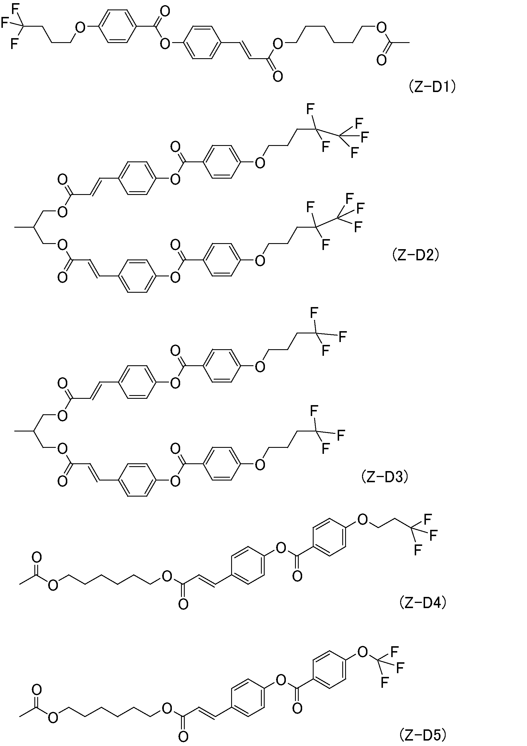


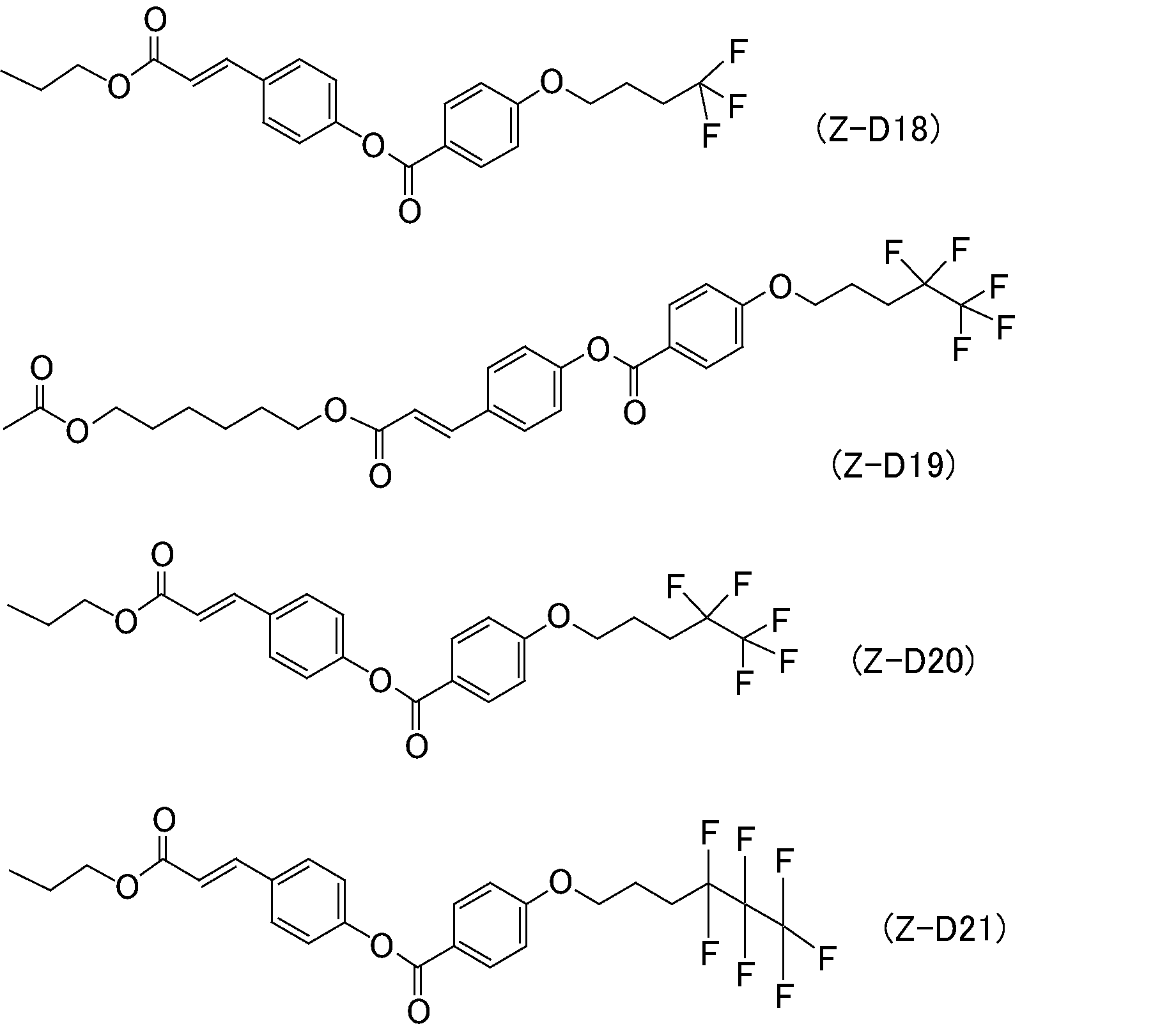
上記W1は、特に限定されず、量子ドットと化学結合できるスペーサー結合基を含む構造であればよい。上記スペーサー結合基としては、例えば、エステル基、アミド基、エーテル基又はチオール基等が挙げられる。上記化学式(A-1)で表される繰り返し構造単位の一部又は全部には、W1が導入されていなくてもよい。
上記量子ドットは、配向膜22を構成する高分子と化学結合していることが好ましい。具体的には、下記化学式(A-2)で表されるように、ポリアミック酸のカルボキシル基と量子ドットの表面の有機鎖の末端のヒドロキシル基とが脱水縮合し、共有結合により結合してもよい。

上記量子ドットは、配向膜を構成する高分子と化学結合ではなく、例えば、下記化学式(A-3)で表されるように、側鎖Zと量子トッドとが分子間力によって結合していてもよいし、主鎖の官能基と分子間力によって結合していてもよい。

上記ポリアミック酸は、一部がイミド化していてもよい。上記ポリアミック酸の初期化学イミド化率は、0%以上、50%以下であることが好ましい。上記ポリアミック酸の初期化学イミド化率のより好ましい上限は、40%である。ポリアミック酸は、加熱又は触媒により脱水閉環することでイミド化することができる。
上記ポリアミック酸は、その重量平均分子量は、2,500以上であることが好ましく、1,000,000以下であることが好ましい。重量平均分子量が1,000,000を超えると、配向膜材料の粘度が配向膜22を成膜できないほど大きくなるおそれがある。なお、重量平均分子量は、GPC(ゲル・パーミエーション・クロマトグラフィー)により決定できる。
上記ポリイミドは、例えば、下記化学式(B-1)で表される繰り返し構造単位を含むものであってもよい。

上記ポリイミドは、上記化学式(A-1)で表される繰り返し構造単位を含むポリアミック酸を、加熱又は触媒により脱水閉環(イミド化)したものであってもよい。なお、上記化学式(A-1)で表される繰り返し構造単位の全てがイミド化していることが好ましいが、一部がイミド化していない部分があってもよい。上記ポリイミドの初期化学イミド化率は、50%を超えることが好ましい。
上記Zは、側鎖を表す。上記化学式(C-1)で表される繰り返し構造単位の一部又は全部には、側鎖Zが導入されていなくてもよい。上記Zには、水平配向官能基、垂直配向官能基、光配向性水平配向官能基、又は、光配向性垂直配向官能基が別途導入されていてもよい。水平配向官能基の具体例としては、上記化学式(Z-A1)~(Z-A8)で表される構造が挙げられる。垂直配向官能基の具体例としては、上記化学式(Z-B1)~(Z-B7)で表される構造が挙げられる。光配向性水平配向官能基の具体例としては、上記化学式(Z-C1)又は(Z-C2)で表される構造が挙げられる。光配向性垂直配向官能基の具体例としては、上記化学式(Z-D1)~(Z-D21)で表される構造が挙げられる。
上記W1は、特に限定されず、量子ドットと化学結合できるスペーサー結合基を含む構造であればよい。上記スペーサー結合基としては、例えば、エステル基、アミド基、エーテル基又はチオール基等が挙げられる。上記量子ドットは、配向膜を構成する高分子と化学結合していることが好ましい。上記化学式(B-1)で表される繰り返し構造単位の一部又は全部には、W1が導入されていなくてもよい。
上記ポリイミドは、その重量平均分子量は、2,500以上であることが好ましく、1,000,000以下であることが好ましい。重量平均分子量が1,000,000を超えると、配向膜材料の粘度が配向膜22を成膜できないほど大きくなるおそれがある。
上記量子ドットは、配向膜を構成する高分子と化学結合ではなく、例えば、下記化学式(B-2)で表されるように、側鎖Zと量子トッドとが分子間力によって結合していてもよいし、主鎖の官能基と分子間力によって結合していてもよい。

上記ポリシロキサンは、例えば、下記化学式(C-1)で表される繰り返し構造単位を含むものであってもよい。

mは、0.001~0.5の範囲の実数であることが好ましく、0.01~0.05の範囲の実数であることがより好ましい。rは、0~0.7の範囲の実数であることが好ましく、0.05~0.5の範囲の実数であることがより好ましい。
上記Zは、側鎖を表す。上記化学式(C-1)で表される繰り返し構造単位の一部又は全部には、側鎖Zが導入されていなくてもよい。上記Zには、水平配向官能基、垂直配向官能基、光配向性水平配向官能基、又は、光配向性垂直配向官能基が別途導入されていてもよい。水平配向官能基の具体例としては、上記化学式(Z-A1)~(Z-A8)で表される構造が挙げられる。垂直配向官能基の具体例としては、上記化学式(Z-B1)~(Z-B7)で表される構造が挙げられる。光配向性水平配向官能基の具体例としては、上記化学式(Z-C1)又は(Z-C2)で表される構造が挙げられる。光配向性垂直配向官能基の具体例としては、上記化学式(Z-D1)~(Z-D21)で表される構造が挙げられる。
上記W1は、特に限定されず、量子ドットと化学結合できるスペーサー結合基を含む構造であればよい。上記スペーサー結合基としては、例えば、エステル基、アミド基、エーテル基又はチオール基等が挙げられる。上記量子ドットは、配向膜を構成する高分子と化学結合していることが好ましい。上記化学式(C-1)で表される繰り返し構造単位の一部又は全部には、W1が導入されていなくてもよい。
化学式(C-1)で表される繰り返し構造単位の一部には、末端にエポキシ基を含有する構造が導入されていてもよい。上記W2は、末端にエポキシ基を含有する構造であることが好ましい。配向膜を構成する高分子がエポキシ基を有することで、量子トッドが有する有機鎖と化学結合することができるためである。
上記化学式(C-1)で表される繰り返し構造単位のより具体的な例としては、例えば、下記化学式(C-2)又は(C-3)で表される繰り返し構造単位が挙げられる。


Zは、下記化学式(Z-D13)又は(Z-E1)で表されるシンナメート基を含む構造を表す。

上記化学式(C-2)で表される繰り返し構造単位では、ポリシロキサンの側鎖のエポキシ基と、量子ドットが表面に有する有機鎖(例えば、カルボキシル基等)との間で共有結合が形成されている。上記化学式(C-3)で表される繰り返し構造単位では、ポリシロキサンと、量子ドットとは、共有結合により結合している。
ポリシロキサンの場合も、上記量子ドットと配向膜を構成するポリシロキサンとが化学結合ではなく、分子間力によって結合していてもよい。
上記光反応基含有ポリマーがポリシロキサンである場合、その重量平均分子量は、2,500以上であることが好ましく、1,000,000以下であることが好ましい。重量平均分子量が1,000,000を超えると、配向膜材料の粘度が配向膜22を成膜できないほど大きくなるおそれがある。
上記ポリビニルは、下記化学式(D-1)で表される繰り返し構造単位を含むものであってもよい。

上記mは、0.001~0.5の範囲の実数であることが好ましく、0.01~0.05の範囲の実数であることがより好ましい。上記rは、0~0.7の範囲の実数であることが好ましく、0.05~0.5の範囲の実数であることがより好ましい。
上記Zは、側鎖を表す。上記化学式(D-1)で表される繰り返し構造単位の一部又は全部には、側鎖Zが導入されていなくてもよい。上記Zには、水平配向官能基、垂直配向官能基、光配向性水平配向官能基、又は、光配向性垂直配向官能基が別途導入されていてもよい。水平配向官能基の具体例としては、上記化学式(Z-A1)~(Z-A8)で表される構造が挙げられる。垂直配向官能基の具体例としては、上記化学式(Z-B1)~(Z-B7)で表される構造が挙げられる。光配向性水平配向官能基の具体例としては、上記化学式(Z-C1)又は(Z-C2)で表される構造が挙げられる。光配向性垂直配向官能基の具体例としては、上記化学式(Z-D1)~(Z-D21)で表される構造が挙げられる。
上記W1は、特に限定されず、量子ドットと化学結合できるスペーサー結合基を含む構造であればよい。上記スペーサー結合基としては、例えば、エステル基、アミド基、エーテル基又はチオール基等が挙げられる。上記量子ドットは、配向膜を構成する高分子と化学結合していることが好ましい。上記化学式(D-1)で表される繰り返し構造単位の一部又は全部には、W1が導入されていなくてもよい。
上記化学式(D-1)で表される繰り返し構造単位の一部には、末端にカルボキシル基を含有する構造が導入されていてもよい。上記W3は、末端にカルボキシル基を含有する構造であることが好ましい。配向膜を構成する高分子がカルボキシル基を有することで、量子トッドが有する有機鎖と化学結合することができるためである。
上記光反応基含有ポリマーがポリビニルである場合、その重量平均分子量は、2,500以上であることが好ましく、1,000,000以下であることが好ましい。重量平均分子量が1,000,000を超えると、配向膜材料の粘度が配向膜22を成膜できないほど大きくなるおそれがある。
ポリビニルの場合も、上記量子ドットと配向膜を構成するポリビニルとが化学結合ではなく、分子間力によって結合していてもよい。
上記化学式(A-1)~(A-3)、(B-1)、(B-2)、(C-1)~(C-3)又は(D-1)で表される高分子が、光反応基を含有する場合、一分子の高分子鎖において、全ての繰り返し構造単位が光配向性官能基を有する必要はなく、少なくとも一部の繰り返し構造単位が光配向性官能基を含んでいればよい。上記高分子は、一種の光配向性官能基を含む繰り返し構造単位のみで構成されていてもよいし、一分子中に異なる光配向性官能基を含む繰り返し構造単位が混在してもよい。更に、一種の光配向性官能基を含む高分子鎖と、異なる他の光配向性官能基を含む高分子鎖とを混合してもよい。
また、上記化学式(A-1)~(A-3)、(B-1)、(B-2)、(C-1)~(C-3)又は(D-1)で表される高分子は、繰り返し構造単位の一部のみに側鎖が導入され、その他の構造単位に側鎖が導入されていない場合、これらの構造単位の配列は特に限定されない。例えば、側鎖が導入された構造単位と、側鎖が導入されていない構造単位とが、交互に配列されていてもよいし、ランダムに配列されていてもよいし、複数の構造単位が連続してブロック単位で配列されていてもよい。
配向膜22は、上記高分子及び量子ドットのほかに、他の成分を更に含有していてもよい。他の成分としては、例えば、硬化剤、硬化促進剤、触媒等を挙げることができる。また、上記高分子以外に、配向膜材料の溶液特性や、配向膜の電気特性をより向上するため、例えば、光配向性官能基、垂直又は水平配向官能基を有さない一般的な配向膜用高分子を含有してもよい。
上記液晶表示装置の表示モードは、ねじれネマティック(TN)モード、イン・プレーン・スイッチング(IPS)モード、フリンジ・フィールド・スイッチング(FFS)モード、電界制御複屈折(ECB)モード、マルチドメイン垂直配向(MVA)モード、又は、4ドメイン・リバース・ねじれネマティック(4D-RTN)モードであることが好ましい。
TNモードでは、一対の基板21の一方に画素電極が設けられ、一対の基板21の他方に共通電極が設けられ、液晶層23中に縦電界が形成される。一対の基板21上の配向膜22は水平配向膜であり、電圧無印加時において、液晶分子の捩れ角が90°となるように配向処理を行う。
FFSモードでは、一対の基板21の少なくとも一方に、面状電極と、スリット電極と、面状電極及びスリット電極の間に配置された絶縁膜とを含む構造(FFS電極構造)が設けられ、液晶層23中に斜め電界(フリンジ電界)が形成される。通常では、液晶層23側から、スリット電極、絶縁膜、面状電極の順に配置される。スリット電極としては、例えば、その全周を電極に囲まれた線状の開口部をスリットとして備えるものや、複数の櫛歯部を備え、かつ櫛歯部間に配置された線状の切れ込みがスリットを構成する櫛型形状のものを用いることができる。
IPSモードでは、一対の基板21の少なくとも一方に一対の櫛形電極が設けられ、液晶層23中に横電界が形成される。一対の櫛形電極としては、例えば、それぞれ複数の櫛歯部を備え、かつ櫛歯部が互いに噛み合うように配置された電極対を用いることができる。
ECBモードは、誘電異方性が正のネマティック液晶を用いた複屈折性を利用したもので、液晶分子への印加電圧によってリタデーションを変化させ、位相差フィルムとの組合せにより液晶層の光の透過及び不透過をコントロールすることにより画像を表示するものである。
MVAモードでは、一対の基板21の一方に画素電極が設けられ、一対の基板21の他方に共通電極が設けられ、液晶層23中に縦電界が形成される。一対の基板21の少なくとも一方に、スリット又リブ等の配向制御手段を設けることで液晶分子の配向方向を制御し、複数のドメインに配向分割させることができる。
4D-RTNモードでは、上記TNモードにおいて、液晶分子の配向方位を4つのドメインに配向分割したものである。配向膜に対して処理方向を行うことで、任意の2つの方向の差が90°の整数倍に略等しい4つの方向に配向分割を行うことができる。
本実施形態の液晶パネル20は、通常では、液晶層23の周囲を囲むように設けられたシール材(図示せず)によって一対の基板21同士が貼り合わされ、液晶層23が所定の領域に保持される。シール材としては、例えば、無機フィラー又は有機フィラー及び硬化剤を含有するエポキシ樹脂等を用いることができる。
また、一対の基板21の液晶層23とは反対側にはそれぞれ、偏光板(直線偏光子)が配置されてもよい。偏光板としては、典型的には、ポリビニルアルコール(PVA)フィルムに、二色性を有するヨウ素錯体等の異方性材料を、吸着配向させたものが挙げられる。通常は、PVAフィルムの両面にトリアセチルセルロースフィルム等の保護フィルムをラミネートして実用に供される。また、偏光板と一対の基板21との間には、位相差フィルム等の光学フィルムが配置されていてもよい。
図1に示したように、本実施形態の液晶表示装置においては、バックライト10が液晶パネルの背面側に配置されている。このような構成を有する液晶表示装置は、一般的に、透過型の液晶表示装置と呼ばれる。バックライト10としては、可視光を含む光を発するものであれば特に限定されず、可視光のみを含む光を発するものであってもよく、可視光及び紫外光の両方を含む光を発するものであってもよい。液晶表示装置によるカラー表示が可能とするためには、白色光を発するバックライト10が好適に用いられる。バックライト10の種類としては、例えば、発光ダイオード(LED)が好適に用いられる。なお、本明細書において、「可視光」とは、波長380nm以上、800nm未満の光(電磁波)を意味する。
本実施形態の液晶表示装置は、青色発光ダイオードを含むバックライトを備えることが好ましい。バックライト10が近紫外線を放出する青色発光ダイオードと、YAG等の蛍光体とを用いて白色を得る疑似白色発光ダイオードを用いた場合、射出光が近紫外線を含むため、液晶パネルを構成する配向膜、液晶材料等の一部がラジカル化しやすく、長期間の使用によりVHRの低下を引き起こし、その結果、焼き付きが発生しやすい。本実施形態の液晶表示装置は、配向膜22が量子ドットを含有するため、青色発光ダイオードを含むバックライトから射出された近紫外~青色のスペクトルを緑~赤のスペクトルに変換することができ、より効果的に焼付きの発生を抑制することができる。
本実施形態の液晶表示装置は、液晶パネル20及びバックライト10の他、TCP(テープ・キャリア・パッケージ)、PCB(プリント配線基板)等の外部回路;視野角拡大フィルム、輝度向上フィルム等の光学フィルム;ベゼル(フレーム)等の複数の部材により構成されるものであり、部材によっては、他の部材に組み込まれていてもよい。既に説明した部材以外の部材については特に限定されず、液晶表示装置の分野において通常使用されるものを用いることができるので、説明を省略する。
本発明の他の一態様は、液晶表示装置の液晶の初期配向を制御するために用いられる配向膜であって、量子ドットを含有する配向膜であってもよい。配向膜の構成は、上記配向膜22と同様であるため詳細な説明は省略する。
以上、本発明の実施形態について説明したが、説明された個々の事項は、すべて本発明全般に対して適用され得るものである。
以下に実施例及び比較例を掲げて本発明を更に詳細に説明するが、本発明はこれらの実施例のみに限定されるものではない。
(合成例1)
合成例1では、ポリアミック酸を主鎖とし、量子ドットが化学結合した水平光配向膜材料を合成した。
合成例1では、トルエンを分散媒とし、分散質として、CdSeから構成されるコロイド粒子がZnSで被覆されたコア・シェル構造(CdSe/ZnS)を有し、キャッピング剤として、ヘキサデシルアミン(HDA)が導入された量子ドット(下記構造(1))を含有する蛍光材料(シグマアルドリッチ社製、CdSe/ZnS480)を用いた。上記量子ドットの発光ピーク波長は、520nmであり、コロイド粒子の粒子径は、2.5nmであった。上記蛍光材料中の固形分量は、5mg/mLであった。
合成例1では、ポリアミック酸を主鎖とし、量子ドットが化学結合した水平光配向膜材料を合成した。
合成例1では、トルエンを分散媒とし、分散質として、CdSeから構成されるコロイド粒子がZnSで被覆されたコア・シェル構造(CdSe/ZnS)を有し、キャッピング剤として、ヘキサデシルアミン(HDA)が導入された量子ドット(下記構造(1))を含有する蛍光材料(シグマアルドリッチ社製、CdSe/ZnS480)を用いた。上記量子ドットの発光ピーク波長は、520nmであり、コロイド粒子の粒子径は、2.5nmであった。上記蛍光材料中の固形分量は、5mg/mLであった。
下記反応式に示したように、上記量子ドットを含有する蛍光材料5mLをテトラヒドロフラン(THF)50mL中に添加し、続いて、3-メルカプト-1-プロパノールを過剰量(0.3g)溶解させたTHF溶液をゆっくり滴下することで、沈殿物が得られた。得られた沈殿物をろ過により回収し、更にTHFで洗浄することで、キャッピング剤の交換を行い、下記構造(2)に示す量子ドットを12mg得た。下記構造(2)に示す量子ドットは、CdSeから構成されるコロイド粒子がZnSで被覆されたコア・シェル構造(CdSe/ZnS)であり、ZnS被膜の表面に、末端にヒドロキシ基を有する有機鎖を有するものであった。

続いて、ポリアミック酸(下記構造(3))が2gの含まれる1-メチルピロリドン溶液(20mL)中に、得られた有機鎖の末端にヒドロキシル基を有するCdSe量子ドット(下記構造(2))が100mg含まれる1-メチルピロリドン溶液5mLを滴下した。続いて、N,N’-ジシクロヘキシルカルボジイミド(DCC)100mgとトリエチルアミン(TEA)100mgとが含まれる1-メチルピロリドン溶液5mLを滴下し、窒素雰囲気下、60℃で24時間反応させた。
続いて、水酸化ナトリウム溶液を滴下し、未反応のカルボキシル基をカルボン酸ナトリウム塩にし、沈殿物を得た。得られた沈殿物を、エバポレーターを用いて回収し、回収物をさらにメタノールを貧溶媒、水を良溶媒とし、溶解再沈を行うことで、量子ドットで修飾した高分子(下記構造(4))を得た。最後に、カチオン交換クロマトグラフィーを用いることで、カルボン酸ナトリウム塩をカルボン酸に戻し、目的の水平光配向膜材料(下記構造(5))を得た。

得られた水平光配向膜材料は、下記化学式(6-1)に示す高分子を含有するものであった。下記化学式(6-1)中、Xは、下記化学式(7)に示す構造であり、Yは、下記化学式(8)に示す構造であった。量子ドットとポリアミック酸とは、量子ドットの表面に有する有機鎖の末端のヒドロキシル基と、ポリアミック酸が有するカルボキシル基とが、エステル結合により結合していた。


(合成例2)
合成例2では、ポリアミック酸を主鎖とし、量子ドットが相互作用により結合した垂直配向膜材料を合成した。
合成例2では、トルエンを分散媒とし、分散質として、CdSeから構成されるコロイド粒子に、キャッピング剤としてヘキサデシルアミン(HDA)が導入されたコア型量子ドット(下記構造(10))を含有する蛍光材料(シグマアルドリッチ社製、662437)を用いた。上記量子ドットの発光ピーク波長は、520nmであり、コロイド粒子の粒子径は、2.5nmであった。上記蛍光材料中の固形分量は、5mg/mLであった。ポリアミック酸としては、下記化学式(9)に示すポリアミック酸を用いた。下記化学式(9)に示すポリアミック酸は、Xとして、下記化学式(12)に示す構造を有し、Yとして、下記化学式(13)に示す構造を有し、Zとして、下記化学式(14)に示すステロイド系垂直配向側鎖を有する。
下記反応式に示したように、上記ポリアミック酸が2gの含まれるNMP/γ-ブチロラクトン混合溶液10mLに、上記量子ドットを含有する蛍光材料10mLを添加した。続いて、エバポレーターを用いて溶媒を濃縮することでトルエンを除去し、下記化学式(11)に示す高分子を含有する垂直配向膜材料を得た。
下記化学式(11)中、Xは、下記化学式(12)に示す構造であり、Yは、下記化学式(13)に示す構造であり、Zは、下記化学式(14)に示す構造であった。量子ドットとポリアミック酸とは、量子ドットの表面に有するヘキサデシル基と、ポリアミック酸の側鎖のステロイド骨格とが分子間力(疎水性相互作用)により結合していた。下記化学式(11)に示す高分子は、下記化学式(14)に示す垂直配向官能基と量子ドットとを含有するユニットを含有するものであった。下記化学式(9)及び(11)中、pは重合度を示し、1以上の整数である。


(合成例3)
合成例3では、ポリシロキサンを主鎖とし、量子ドットが化学結合した垂直光配向膜材料を合成した。
合成例3では、トルエンを分散媒とし、分散質として、CdSeから構成されるコロイド粒子に、キャッピング剤として、カルボキシル基が導入されたコア型量子ドット(下記構造(16))を含有する蛍光材料(シグマアルドリッチ社製)を用いた。上記量子ドットの発光ピーク波長は、520nmであり、コロイド粒子の粒子径は、2.5nmであった。上記蛍光材料中の固形分量は、5mg/mLであった。ポリシロキサンとしては、下記化学式(15)に示すポリシロキサンを用いた。下記化学式(15)に示すポリシロキサンは、Zとして、下記化学式(18)に示すシンナメート基を有する光配向性垂直配向側鎖を有する。
下記反応式に示したように、上記ポリシロキサンが2gの含まれるトルエン溶液10mL中に、上記量子ドットを含有する蛍光材料10mLを滴下し、その後、70℃で5時間反応させた。反応終了後、エーテルを貧溶媒、NMPを良溶媒とし、溶解再沈を行うことで、量子ドットを約25mol%修飾した下記化学式(17)に示した高分子を含有する垂直光配向膜材料を得た。下記化学式(15)及び(17)中、pは重合度を示し、1以上の整数である。
下記化学式(17)中、Zは、下記化学式(18)に示す構造であった。量子ドットとポリシロキサンとは、量子ドットの表面に有する有機鎖の末端のカルボキシル基と、ポリシロキサンが有するエポキシ基とが、エステル結合により結合していた。

(実施例1-1)
イン・プレーン・スイッチング(IPS)モードの液晶表示装置を以下の方法により実際に作製した。まず、図4に示したような、TFT、IPS電極構造等を備えるTFT基板、及び、電極を有さず、ブラックマトリクス、カラーフィルタ等を備えるカラーフィルタ基板(CF基板)を用意した。
イン・プレーン・スイッチング(IPS)モードの液晶表示装置を以下の方法により実際に作製した。まず、図4に示したような、TFT、IPS電極構造等を備えるTFT基板、及び、電極を有さず、ブラックマトリクス、カラーフィルタ等を備えるカラーフィルタ基板(CF基板)を用意した。
TFT基板及びCF基板の各々の表面上に、合成例1で得られた水平光配向膜材料を塗布し、60℃90秒間の仮焼成を行った。続いて、光配向処理として、両基板の表面に塗布した配向膜材料に対して、主波長が365nmである直線偏光紫外光を2J/cm2の強度で照射した。直線偏光紫外光の照射により、アゾベンゼン構造においてトランス-シス異性化反応が生じ、配向規制力が発現した。その後、230℃40分間の本焼成を行った。本焼成により、ポリアミック酸構造の一部においてイミド化(脱水閉環反応)が起こり、ポリイミド構造が形成された。以上によって、光照射によって充分な配向規制力を発現させた水平光配向膜が得られた。本焼成後の上記配向膜の膜厚は100nmであった。
得られた水平光配向膜は、下記化学式(6-1)に示す構造を有するものであった。下記化学式(6-1)中、Xは、下記化学式(7)に示す構造であり、Yは、下記化学式(8)に示す構造であった。


上記化学式(6-1)に示す高分子は、ポリアミック酸を主鎖とし、量子ドットの表面に有する有機鎖の末端のヒドロキシル基と、ポリアミック酸が有するカルボキシル基とが、エステル結合により結合していた。また、上記化学式(6-1)に示す高分子は、上記化学式(8)に示す光配向性官能基(アゾベンゼン基)及び水平配向官能基(-H)を含有するユニットと、上記化学式(8)に示す光配向性官能基、水平配向官能基(-H)、及び、量子ドットを含有するユニットとの共重合体であった。
続いて、一方の基板に、ディスペンサを用いて、紫外線硬化性シール剤(積水化学社製、商品名:フォトレックS-WB)を描画した。もう一方の基板上の所定の位置に、誘電率異方性が負(△ε=-3.7)である液晶分子を含有する液晶組成物を滴下した。その後、真空下にて両基板を貼り合わせ、シール剤を紫外光にて硬化させた。最後に、130℃で40分間加熱し、液晶を等方相にする再配向処理を行い、その後室温まで冷却した。
更に、偏光軸がクロスニコルの関係になるように、TFT基板の裏面側(バックライト光の入射面側)及びCF基板の観察面側(バックライト光の出射面側)に、一対の偏光板を貼り付け、液晶パネルを作製した。続いて、液晶パネルの背面側に、疑似白色LEDを備えるバックライトを取り付け、実施例1-1の液晶表示装置が完成した。
(実施例1-2)
発光ピーク波長及び粒子径が異なる量子ドットを用いた点以外は、実施例1-1と同様にして、実施例1-2の液晶表示装置を作製した。
発光ピーク波長及び粒子径が異なる量子ドットを用いた点以外は、実施例1-1と同様にして、実施例1-2の液晶表示装置を作製した。
量子ドットとして、CdSeから構成されるコロイド粒子がZnSで被覆されたコア・シェル構造(CdSe/ZnS)を有し、キャッピング剤としてヘキサデシルアミン(HDA)が導入され、発光ピーク波長が、610nmであり、コロイド粒子の粒子径が、5.0nmであるコア・シェル型量子ドット(シグマアルドリッチ社製、662488)を用いた点以外は、合成例1と同様にして、水平光配向膜材料を合成した。得られた水平光配向膜材料を用いて、実施例1-1と同様にして、実施例1-2の液晶表示装置を作製した。
(比較例1)
量子ドットを含有する蛍光材料を添加しなかった点以外は、実施例1-1と同様にして、比較例1の液晶表示装置を作製した。
量子ドットを含有する蛍光材料を添加しなかった点以外は、実施例1-1と同様にして、比較例1の液晶表示装置を作製した。
<バックライト上での高温試験>
実施例1-1、1-2、及び、比較例1で作製したIPSモードの液晶セルの耐熱性を評価するため、点灯したバックライト上に液晶セルを配置し、液晶セルの温度を75℃に昇温した状態で5000時間放置する試験を行った。放置の前後で電圧保持率(VHR)及びコントラストの測定を行った。結果を下記表2に示した。なお、VHRは東陽テクニカ社製の6254型VHR測定システムを用いて、1V、70℃の条件で測定した。コントラスト測定は、トプコンテクノハウス社製の分光放射計のSR-UL1Rを用いて、25℃環境下で測定した。
実施例1-1、1-2、及び、比較例1で作製したIPSモードの液晶セルの耐熱性を評価するため、点灯したバックライト上に液晶セルを配置し、液晶セルの温度を75℃に昇温した状態で5000時間放置する試験を行った。放置の前後で電圧保持率(VHR)及びコントラストの測定を行った。結果を下記表2に示した。なお、VHRは東陽テクニカ社製の6254型VHR測定システムを用いて、1V、70℃の条件で測定した。コントラスト測定は、トプコンテクノハウス社製の分光放射計のSR-UL1Rを用いて、25℃環境下で測定した。

上記表2に示したように、量子ドットを配向膜材料中に導入していない比較例1では、上記高温試験後に、VHRおよびコントラストが顕著に低下した。これは、光源として青色LEDを含むバックライト光に含まれる紫外線成分により、ネガ型液晶成分内の芳香環とアルコキシ基よりラジカルが形成され、不純物イオンが生成し、液晶層内に溶出したためと考えられる。一方、量子ドットを配向膜材料中に化学結合により導入した実施例1-1及び1-2では、上記バックライト上での高温試験を行った後も、比較的高いVHRとコントラスト値を示した。これは、バックライト光に含まれる紫外線成分が、量子ドットにより低エネルギーの可視光成分へ変換され、ネガ型液晶成分からのラジカル発生を抑制したためと考えられる。
(実施例2-1)
フリンジ・フィールド・スイッチング(FFS)モードの液晶表示装置を以下の方法により実際に作製した。まず、図4に示したような、TFT、FFS電極構造等を備えるTFT基板、及び、電極を有さず、ブラックマトリクス、カラーフィルタ等を備えるカラーフィルタ基板(CF基板)を用意した。
フリンジ・フィールド・スイッチング(FFS)モードの液晶表示装置を以下の方法により実際に作製した。まず、図4に示したような、TFT、FFS電極構造等を備えるTFT基板、及び、電極を有さず、ブラックマトリクス、カラーフィルタ等を備えるカラーフィルタ基板(CF基板)を用意した。
量子ドットとして、InPから構成されるコロイド粒子に、キャッピング剤としてヘキサデシルアミン(HDA)が導入され、発光ピーク波長が、530nmであり、コロイド粒子の粒子径が、2.7nmであるコア型量子ドット(シグマアルドリッチ社製)を用いた点以外は、合成例1と同様にして、水平光配向膜材料を合成した。
得られた水平光配向膜材料を用いて、実施例1-1と同様にして、TFT基板及びCF基板の各々の表面上に水平光配向膜を形成した。本焼成後の上記配向膜の膜厚は100nmであった。その後、実施例1-1と同様にして、液晶パネルを作製し、液晶パネルの背面側に、疑似白色LEDを備えるバックライトを取り付け、実施例2-1の液晶表示装置が完成した。
(実施例2-2)
発光ピーク波長及び粒子径が異なる量子ドットを用いた点以外は、実施例2-1と同様にして、実施例2-2の液晶表示装置を作製した。
発光ピーク波長及び粒子径が異なる量子ドットを用いた点以外は、実施例2-1と同様にして、実施例2-2の液晶表示装置を作製した。
量子ドットとして、InPから構成されるコロイド粒子に、キャッピング剤としてヘキサデシルアミン(HDA)が導入され、発光ピーク波長が、600nmであり、コロイド粒子の粒子径が、5.4nmであるコア型量子ドット(シグマアルドリッチ社製)を用いた点以外は、合成例1と同様にして、水平光配向膜材料を合成した。得られた水平光配向膜材料を用いて、実施例2-1と同様にして、実施例2-2の液晶表示装置を作製した。
(比較例2)
量子ドットを含有する蛍光材料を添加しなかった点以外は、実施例2-1と同様にして、比較例2の液晶表示装置を作製した。
量子ドットを含有する蛍光材料を添加しなかった点以外は、実施例2-1と同様にして、比較例2の液晶表示装置を作製した。
<バックライト上での高温試験>
実施例2-1、2-2及び比較例2で作製したFFSモードの液晶セルについて、実施例1-1と同様の評価試験を行った結果を下記表3に示した。
実施例2-1、2-2及び比較例2で作製したFFSモードの液晶セルについて、実施例1-1と同様の評価試験を行った結果を下記表3に示した。

上記表3に示したように、量子ドットを配向膜材料中に導入していない比較例2では、上記高温試験後に、VHR及びコントラストが顕著に低下した。一方、量子ドットを配向膜材料中に化学結合により導入した実施例2-1及び2-2では、上記高温試験を行った後も、比較的高いVHRとコントラスト値を示した。これにより、配向膜中に量子ドットを含有することで、VHR及びコントラストの低下を抑制できることがわかった。更に、実施例1-1、1-2と、実施例2-1、2-2との比較により、吸収波長に紫外領域を含み、発光波長が可視光領域(500nm以上)である量子ドットであれば、量子ドットの原子種・組成への依存性がなく、VHR及びコントラストの低下を抑制する信頼性改善効果があることが示された。
(実施例3-1)
フリンジ・フィールド・スイッチング(FFS)モードの液晶表示装置を以下の方法により実際に作製した。まず、図4に示したような、TFT、FFS電極構造等を備えるTFT基板、及び、電極を有さず、ブラックマトリクス、カラーフィルタ等を備えるカラーフィルタ基板(CF基板)を用意した。
フリンジ・フィールド・スイッチング(FFS)モードの液晶表示装置を以下の方法により実際に作製した。まず、図4に示したような、TFT、FFS電極構造等を備えるTFT基板、及び、電極を有さず、ブラックマトリクス、カラーフィルタ等を備えるカラーフィルタ基板(CF基板)を用意した。
水平光配向膜材料としては、光官能基としてアゾベンゼン基を有するポリアミック酸に、量子ドットを添加したものを用いた。量子ドットとして、CdSeから構成されるコロイド粒子がZnSで被覆されたコア・シェル構造(CdSe/ZnS)を有し、キャッピング剤としてヘキサデシルアミン(HDA)が導入され、発光ピーク波長が、530nmであり、コロイド粒子の粒子径が、3.3nmであるコア・シェル型量子ドット(シグマアルドリッチ社製、694649)を用いた。
上記水平光配向膜材料を用いて、実施例1-1と同様にして、TFT基板及びCF基板の各々の表面上に水平光配向膜を形成した。本焼成後の上記配向膜の膜厚は100nmであった。
得られた水平光配向膜は、下記化学式(6-2)に示す構造を有するものであった。下記化学式(6-2)中、Xは、下記化学式(7)に示す構造であり、Yは、下記化学式(8)に示す構造であった。


上記化学式(6-2)に示す高分子は、ポリアミック酸を主鎖とし、量子ドットの表面に有する有機鎖の末端のヒドロキシル基と、ポリアミック酸が有するカルボキシル基とが、分子間力(水素結合)により結合していた。また、上記化学式(6-2)に示す高分子は、上記化学式(8)に示す光配向性官能基(アゾベンゼン基)を含有するユニットと、上記化学式(8)に示す光配向性官能基、及び、量子ドットを含有するユニットとの共重合体から成る水平配向用高分子であった。
その後、実施例1-1と同様にして、液晶パネルを作製し、液晶パネルの背面側に、疑似白色LEDを備えるバックライトを取り付け、実施例3-1の液晶表示装置が完成した。
(実施例3-2)
発光ピーク波長及び粒子径が異なる量子ドットを用いた点以外は、実施例3-1と同様にして、実施例3-2の液晶表示装置を作製した。
発光ピーク波長及び粒子径が異なる量子ドットを用いた点以外は、実施例3-1と同様にして、実施例3-2の液晶表示装置を作製した。
量子ドットとして、CdSeから構成されるコロイド粒子がZnSで被覆されたコア・シェル構造(CdSe/ZnS)を有し、キャッピング剤としてヘキサデシルアミン(HDA)が導入され、発光ピーク波長が、610nmであり、コロイド粒子の粒子径が、5.2nmであるコア・シェル型量子ドット(シグマアルドリッチ社製)を用いた。実施例3-1と同様に、光官能基としてアゾベンゼン基を有するポリアミック酸に、上記量子トッドを添加して、水平配向膜材料を得た。得られた水平光配向膜材料を用いて、実施例3-1同様にして、実施例3-2の液晶表示装置を作製した。
(比較例3)
量子ドットを含有する蛍光材料を添加しなかった点以外は、実施例3-1と同様にして、比較例3の液晶表示装置を作製した。
量子ドットを含有する蛍光材料を添加しなかった点以外は、実施例3-1と同様にして、比較例3の液晶表示装置を作製した。
<バックライト上での高温試験>
実施例3-1、3-2及び比較例3で作製したFFSモードの液晶セルについて、実施例1-1と同様の評価試験を行った結果を下記表4に示した。
実施例3-1、3-2及び比較例3で作製したFFSモードの液晶セルについて、実施例1-1と同様の評価試験を行った結果を下記表4に示した。

上記表4に示したように、量子ドットを配向膜材料中に導入していない比較例3では、上記高温試験後に、VHR及びコントラストが顕著に低下した。一方、量子ドットを配向膜材料中に分子間力(水素結合)により導入した実施例3-1及び3-2では、上記高温試験を行った後も、比較的高いVHRとコントラスト値を示した。これにより、配向膜中に量子ドットを含有することで、VHR及びコントラストの低下を抑制できることが分かった。更に、実施例1-1、1-2と、実施例3-1、3-2との比較により、配向膜を構成する高分子と量子ドットとが、化学結合していても、分子間力により結合していても、VHR及びコントラストの低下を抑制する信頼性改善効果があることが分かった。また、吸収波長に紫外領域を含み、発光波長が可視光領域(500nm以上)である量子ドットであれば、量子ドットの原子種・組成への依存性がなく、上記信頼性改善効果があることが示された。
(実施例4-1)
マルチドメイン垂直配向(MVA)モードの液晶表示装置を以下の方法により実際に作製した。まず、図3に示したような、TFT、画素電極等を備えるTFT基板、及び、スリットを有する対向電極、ブラックマトリクス、カラーフィルタ等を備えるカラーフィルタ基板(CF基板)を用意した。
マルチドメイン垂直配向(MVA)モードの液晶表示装置を以下の方法により実際に作製した。まず、図3に示したような、TFT、画素電極等を備えるTFT基板、及び、スリットを有する対向電極、ブラックマトリクス、カラーフィルタ等を備えるカラーフィルタ基板(CF基板)を用意した。
TFT基板及びCF基板の各々の表面上に、合成例2で得られた垂直配向膜材料を塗布し、90℃5分間の仮焼成を行い、続いて、200℃40分間の本焼成を行った。本焼成により、ポリアミック酸構造の一部においてイミド化(脱水閉環反応)が起こり、ポリイミド構造が形成された。本焼成後の上記配向膜の膜厚は100nmであった。
得られた垂直配向膜は、下記化学式(11)に示す高分子を含有するものであった。下記化学式(11)中、Xは、下記化学式(12)に示す構造であり、Yは、下記化学式(13)に示す構造であり、Zは、下記化学式(14)に示す構造であった。


上記化学式(11)に示す高分子は、ポリアミック酸を主鎖とし、量子ドットの表面に有するヘキサデシル基と、ポリアミック酸の側鎖のステロイド骨格とが分子間力(疎水性相互作用)により結合していた。また、上記化学式(11)に示した高分子は、上記式(14)に示す光配向性垂直配向官能基(ステロイド骨格)及び量子ドットを含有するユニットを含有するものであった。
その後、実施例1-1と同様にして、液晶パネルを作製し、液晶パネルの背面側に、疑似白色LEDを備えるバックライトを取り付け、実施例4-1の液晶表示装置が完成した。
(実施例4-2)
発光ピーク波長及び粒子径が異なる量子ドットを用いた点以外は、実施例4-1と同様にして、実施例4-2の液晶表示装置を作製した。
発光ピーク波長及び粒子径が異なる量子ドットを用いた点以外は、実施例4-1と同様にして、実施例4-2の液晶表示装置を作製した。
量子ドットとして、CdSeから構成されるコロイド粒子に、キャッピング剤としてヘキサデシルアミン(HDA)が導入され、発光ピーク波長が、610nmであり、コロイド粒子の粒子径が、5.0nmであるコア型量子ドット(シグマアルドリッチ社製、662488)を用いた点以外は、合成例2と同様にして、垂直配向膜材料を合成した。得られた垂直配向膜材料を用いて、実施例4-1同様にして、実施例4-2の液晶表示装置を作製した。
(比較例4)
量子ドットを含有する蛍光材料を添加しなかった点以外は、実施例4-1と同様にして、比較例4の液晶表示装置を作製した。
量子ドットを含有する蛍光材料を添加しなかった点以外は、実施例4-1と同様にして、比較例4の液晶表示装置を作製した。
<バックライト上での高温試験>
実施例4-1、4-2及び比較例4で作製したMVAモードの液晶セルについて、実施例1-1と同様の評価試験を行った結果を下記表5に示した。
実施例4-1、4-2及び比較例4で作製したMVAモードの液晶セルについて、実施例1-1と同様の評価試験を行った結果を下記表5に示した。

上記表5に示したように、垂直配向膜材料中に量子ドットを導入した実施例4-1及び4-2では、上記高温試験を行った後も、VHR及びコントラストの低下は、ほぼ確認されなかった。一方、量子ドットを導入しなかった比較例4では、上記高温試験後に、VHR及びコントラストが低下した。配向膜材料中に量子ドットを導入しない場合、バックライト光に含まれる紫外線成分により、ネガ型液晶成分内の芳香環とアルコキシ基よりラジカルが形成され、不純物イオンが生成し、液晶層内に溶出したため、VHR及びコントラストが低下したと考えられる。一方、配向膜材料中に量子ドットを導入すると、バックライト光に含まれる紫外線成分が量子ドットにより低エネルギーの可視光成分へ変換され、ネガ型液晶成分からのラジカル発生を抑制したため、VHR及びコントラストの低下が抑制されたと考えられる。
(実施例5-1)
4D-RTNモードの液晶表示装置を以下の方法により実際に作製した。まず、図3に示したような、TFT、画素電極等を備えるTFT基板、及び、ITO電極、ブラックマトリクス、カラーフィルタ等を備えるカラーフィルタ基板(CF基板)を用意した。
4D-RTNモードの液晶表示装置を以下の方法により実際に作製した。まず、図3に示したような、TFT、画素電極等を備えるTFT基板、及び、ITO電極、ブラックマトリクス、カラーフィルタ等を備えるカラーフィルタ基板(CF基板)を用意した。
TFT基板及びCF基板の各々の表面上に、合成例3で得られた垂直光配向膜材料と、下地層としてポリアミック酸系配向剤を混合した配向膜材料を塗布し、60℃5分間の仮焼成を行った。続いて、光配向処理として、両基板の表面に塗布した配向膜材料に対して、主波長が330nmである直線偏光紫外光を50mJ/cm2の強度で照射した。直線偏光紫外光の照射により、配向処理を施し、チルト角が88.6°程度になるように、4つの配向領域に光配向処理を行った。以上によって、配向規制力を発現させた垂直光配向膜が得られた。上記配向膜の膜厚は100nmであった。なお、下地層として用いたポリアミック酸は、光反応基及び垂直又は水平配向官能基を有さないものであった。
得られた垂直光配向膜は、下記化学式(17)に示す構造を有するものであった。下記化学式(17)中、Zは、下記化学式(18)に示す構造であった。
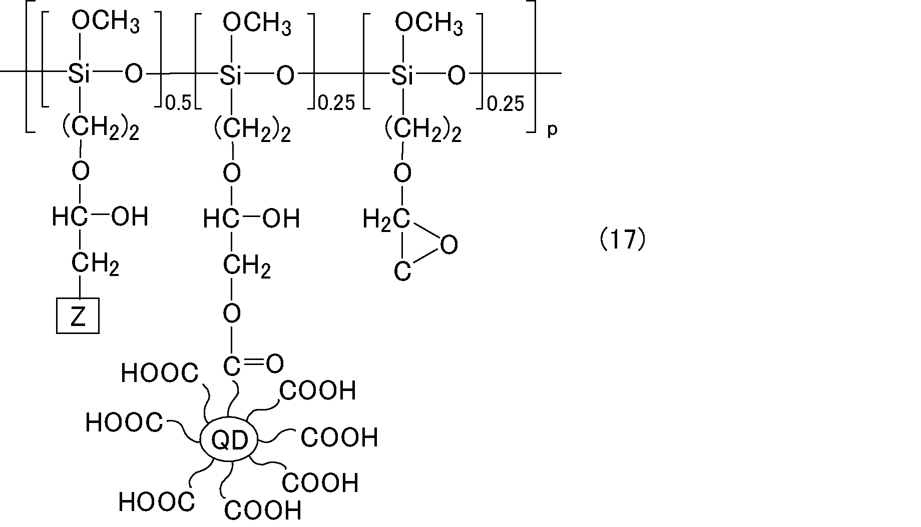
上記化学式(17)に示す高分子は、ポリシロキサンを主鎖とし、ポリシロキサンが有するエポキシ基と、量子ドットの表面に有する有機鎖の末端のカルボキシル基とが、エステル結合により結合していた。また、上記化学式(17)に示す高分子は、上記式(18)に示す光配向性官能基(シンナメート基)を含む垂直配向官能基を含有するユニットと、量子ドットを含有するユニットとの共重合体であった。
その後、実施例1-1と同様にして、液晶パネルを作製し、液晶パネルの背面側に、疑似白色LEDを備えるバックライトを取り付け、実施例5-1の液晶表示装置が完成した。
(実施例5-2)
発光ピーク波長及び粒子径が異なる量子ドットを用いた点以外は、実施例5-1と同様にして、実施例5-2の液晶表示装置を作製した。
発光ピーク波長及び粒子径が異なる量子ドットを用いた点以外は、実施例5-1と同様にして、実施例5-2の液晶表示装置を作製した。
量子ドットとして、CdSeから構成されるコロイド粒子に、キャッピング剤としてヘキサデシルアミン(HDA)が導入され、発光ピーク波長が、610nmであり、コロイド粒子の粒子径が、5.0nmであるコア型量子ドット(シグマアルドリッチ社製、662488)を用いた点以外は、合成例3と同様にして、垂直光配向膜材料を合成した。得られた垂直光配向膜材料を用いて、実施例5-1同様にして、実施例5-2の液晶表示装置を作製した。
(比較例5)
量子ドットを含有する蛍光材料を添加しなかった点以外は、実施例5-1と同様にして、比較例5の液晶表示装置を作製した。
量子ドットを含有する蛍光材料を添加しなかった点以外は、実施例5-1と同様にして、比較例5の液晶表示装置を作製した。
<バックライト上での高温試験>
実施例5-1、5-2及び比較例5で作製した4D-RTNモードの液晶セルについて、実施例1-1と同様の評価試験を行った結果を下記表6に示した。
実施例5-1、5-2及び比較例5で作製した4D-RTNモードの液晶セルについて、実施例1-1と同様の評価試験を行った結果を下記表6に示した。

上記表6に示したように、垂直光配向膜材料中に量子ドットを導入した実施例5-1及び5-2では、上記高温試験を行った後も、VHR及びコントラストの低下は、ほぼ確認されなかった。一方、量子ドットを導入しなかった比較例5では、上記高温試験後に、VHR及びコントラストが低下した。配向膜材料中に量子ドットを導入しない場合、バックライト光に含まれる紫外線成分により、ネガ型液晶成分内の芳香環とアルコキシ基よりラジカルが形成され、不純物イオンが生成し、液晶層内に溶出したため、VHR及びコントラストが低下したと考えられる。一方、配向膜材料中に量子ドットを導入すると、バックライト光に含まれる紫外線成分が量子ドットにより低エネルギーの可視光成分へ変換され、ネガ型液晶成分からのラジカル発生を抑制したため、VHR及びコントラストの低下が抑制されたと考えられる。
[付記]
本発明の一態様は、一対の基板と、上記一対の基板間に挟持され液晶分子を含有する液晶層と、上記一対の基板の少なくとも一方と上記液晶層との間に配置された配向膜とを備え、上記配向膜は、量子ドットを含有する液晶表示装置であってもよい。
本発明の一態様は、一対の基板と、上記一対の基板間に挟持され液晶分子を含有する液晶層と、上記一対の基板の少なくとも一方と上記液晶層との間に配置された配向膜とを備え、上記配向膜は、量子ドットを含有する液晶表示装置であってもよい。
上記一態様において、上記量子ドットは、表面に有機鎖を有することが好ましい。上記量子ドットは、配向膜を構成する高分子と化学結合していることが好ましい。上記量子ドットは、発光ピーク波長が、400nmよりも長波長であることが好ましい。上記量子ドットは、カドミウムセレン、カドミウムテルル、硫化カドミウム、及び、リン化インジウムからなる群より選ばれる少なくとも1種の化合物を含むことが好ましい。
上記一態様において、上記配向膜は、上記配向膜に隣接する上記液晶分子を、上記配向膜の表面に対して水平に配向させることが好ましい。上記配向膜は、水平配向官能基を含有するユニットと量子ドットを含有するユニットを含有することが好ましい。
上記一態様において、上記配向膜は、上記配向膜に隣接する上記液晶分子を、上記配向膜の表面に対して垂直に配向させることが好ましい。上記配向膜は、垂直配向官能基を含有するユニットと量子ドットを含有するユニットを含有することが好ましい。
上記一態様において、上記配向膜は、光配向性官能基を含有する光配向膜であることが好ましい。上記光配向性官能基は、シンナメート基、カルコン基、クマリン基、アゾベンゼン基、及び、トラン基からなる群より選ばれる少なくとも1種の光配向性官能基であることが好ましい。上記光配向性官能基は、シンナメート基であることがより好ましい。上記光配向膜は、光配向性官能基を含有するユニットと量子ドットを含有するユニットを含有することが好ましい。
上記一態様において、上記配向膜は、ポリアミック酸、ポリイミド、ポリシロキサン、及び、ポリビニルからなる群より選ばれる少なくとも1種の高分子を含有することが好ましい。
上記一態様において、上記液晶分子は、負の誘電率異方性を有することが好ましい。
上記液晶表示装置は、更に、青色発光ダイオードを含むバックライトを備えることが好ましい。
上記液晶表示装置の表示モードは、ねじれネマティック(TN)モード、イン・プレーン・スイッチング(IPS)モード、フリンジ・フィールド・スイッチング(FFS)モード、電界制御複屈折(ECB)モード、マルチドメイン垂直配向(MVA)モード、又は、4ドメイン・リバース・ねじれネマティック(4D-RTN)モードであることが好ましい。
本発明の他の一態様は、液晶表示装置の液晶の初期配向を制御するために用いられる配向膜であって、量子ドットを含有する配向膜であってもよい。
上記他の一態様において、上記量子ドットは、表面に有機鎖を有することが好ましい。上記量子ドットは、配向膜を構成する高分子と化学結合していることが好ましい。上記量子ドットは、カドミウムセレン、カドミウムテルル、硫化カドミウム、及び、リン化インジウムからなる群より選ばれる少なくとも1種の化合物を含むことが好ましい。
上記他の一態様において、上記配向膜は、垂直配向官能基又は水平配向官能基を含有するユニットと、量子ドットを含有するユニットを含むことが好ましい。
上記他の一態様において、上記配向膜は、光配向性官能基を含む光配向膜であることが好ましい。上記光配向性官能基は、シンナメート基、カルコン基、クマリン基、アゾベンゼン基、及び、トラン基からなる群より選ばれる少なくとも1種の光配向性官能基であることが好ましい。上記光配向性官能基は、シンナメート基であることがより好ましい。
上記他の一態様において、上記配向膜は、光配向性官能基を含有するユニットと量子ドットを含有するユニットを含むことが好ましい。
上記他の一態様において、上記配向膜は、ポリアミック酸、ポリイミド、ポリシロキサン、及び、ポリビニルからなる群より選ばれる少なくとも1種の高分子を含むことが好ましい。
以上に示した本発明の各態様は、本発明の要旨を逸脱しない範囲において適宜組み合わされてもよい。
10:バックライト
20:液晶パネル
21:基板
22:配向膜
23:液晶層
31:ゲート信号線
32:ゲート絶縁膜
33:ソース信号線
34:ドレイン電極
35:半導体層
36:第一層間膜
37:第一電極
38:第二層間膜
39:第二電極
20:液晶パネル
21:基板
22:配向膜
23:液晶層
31:ゲート信号線
32:ゲート絶縁膜
33:ソース信号線
34:ドレイン電極
35:半導体層
36:第一層間膜
37:第一電極
38:第二層間膜
39:第二電極
Claims (17)
- 一対の基板と、前記一対の基板間に挟持され液晶分子を含有する液晶層と、前記一対の基板の少なくとも一方と前記液晶層との間に配置された配向膜とを備え、
前記配向膜は、量子ドットを含有することを特徴とする液晶表示装置。 - 前記量子ドットは、表面に有機鎖を有することを特徴とする請求項1に記載の液晶表示装置。
- 前記量子ドットは、配向膜を構成する高分子と化学結合していることを特徴とする請求項2に記載の液晶表示装置。
- 前記量子ドットは、発光ピーク波長が、400nmよりも長波長であることを特徴とする請求項1~3のいずれかに記載の液晶表示装置。
- 前記量子ドットは、カドミウムセレン、カドミウムテルル、硫化カドミウム、及び、リン化インジウムからなる群より選ばれる少なくとも1種の化合物を含むことを特徴とする請求項1~4のいずれかに記載の液晶表示装置。
- 前記配向膜は、前記配向膜に隣接する前記液晶分子を、前記配向膜の表面に対して水平に配向させることを特徴とする請求項1~5のいずれかに記載の液晶表示装置。
- 前記配向膜は、水平配向官能基を含有するユニットと量子ドットを含有するユニットを含有することを特徴とする請求項6に記載の液晶表示装置。
- 前記配向膜は、前記配向膜に隣接する前記液晶分子を、前記配向膜の表面に対して垂直に配向させることを特徴とする請求項1~5のいずれかに記載の液晶表示装置。
- 前記配向膜は、垂直配向官能基を含有するユニットと量子ドットを含有するユニットを含有することを特徴とする請求項8に記載の液晶表示装置。
- 前記配向膜は、光配向性官能基を含有する光配向膜であることを特徴とする請求項1~9のいずれかに記載の液晶表示装置。
- 前記光配向性官能基は、シンナメート基、カルコン基、クマリン基、アゾベンゼン基、及び、トラン基からなる群より選ばれる少なくとも1種の光配向性官能基であることを特徴とする請求項10に記載の液晶表示装置。
- 前記光配向性官能基は、シンナメート基であることを特徴とする請求項10に記載の液晶表示装置。
- 前記光配向膜は、光配向性官能基を含有するユニットと量子ドットを含有するユニットを含有することを特徴とする請求項10~12のいずれかに記載の液晶表示装置。
- 前記配向膜は、ポリアミック酸、ポリイミド、ポリシロキサン、及び、ポリビニルからなる群より選ばれる少なくとも1種の高分子を含有することを特徴とする請求項1~13のいずれかに記載の液晶表示装置。
- 前記液晶分子は、負の誘電率異方性を有することを特徴とする請求項1~14のいずれかに記載の液晶表示装置。
- 更に、青色発光ダイオードを含むバックライトを備えることを特徴とする請求項1~15のいずれかに記載の液晶表示装置。
- 液晶表示装置の液晶の初期配向を制御するために用いられる配向膜であって、
量子ドットを含有することを特徴とする配向膜。
Priority Applications (2)
| Application Number | Priority Date | Filing Date | Title |
|---|---|---|---|
| US16/083,851 US10831066B2 (en) | 2016-03-10 | 2017-03-03 | Liquid crystal display device and alignment film |
| CN201780016311.9A CN108780244A (zh) | 2016-03-10 | 2017-03-03 | 液晶显示装置及取向膜 |
Applications Claiming Priority (2)
| Application Number | Priority Date | Filing Date | Title |
|---|---|---|---|
| JP2016047405 | 2016-03-10 | ||
| JP2016-047405 | 2016-03-10 |
Publications (1)
| Publication Number | Publication Date |
|---|---|
| WO2017154747A1 true WO2017154747A1 (ja) | 2017-09-14 |
Family
ID=59790436
Family Applications (1)
| Application Number | Title | Priority Date | Filing Date |
|---|---|---|---|
| PCT/JP2017/008396 WO2017154747A1 (ja) | 2016-03-10 | 2017-03-03 | 液晶表示装置及び配向膜 |
Country Status (3)
| Country | Link |
|---|---|
| US (1) | US10831066B2 (ja) |
| CN (1) | CN108780244A (ja) |
| WO (1) | WO2017154747A1 (ja) |
Cited By (2)
| Publication number | Priority date | Publication date | Assignee | Title |
|---|---|---|---|---|
| WO2019189270A1 (ja) * | 2018-03-27 | 2019-10-03 | 日立化成株式会社 | 波長変換部材、バックライトユニット、及び画像表示装置 |
| WO2019186726A1 (ja) * | 2018-03-27 | 2019-10-03 | 日立化成株式会社 | 波長変換部材、バックライトユニット、及び画像表示装置 |
Families Citing this family (5)
| Publication number | Priority date | Publication date | Assignee | Title |
|---|---|---|---|---|
| CN106773332A (zh) * | 2016-12-26 | 2017-05-31 | 深圳市华星光电技术有限公司 | 照射灯、液晶配向的方法及装置 |
| CN111028684B (zh) * | 2019-12-06 | 2021-08-03 | 深圳市华星光电半导体显示技术有限公司 | 柔性基板及其制备方法 |
| CN111552121B (zh) * | 2020-05-08 | 2021-09-24 | 深圳市华星光电半导体显示技术有限公司 | 配向膜、显示面板及其制备方法 |
| CN111653670A (zh) * | 2020-06-15 | 2020-09-11 | 京东方科技集团股份有限公司 | 一种光电器件及其制备方法、光电探测器 |
| CN114675439B (zh) * | 2022-03-30 | 2023-11-28 | 广州华星光电半导体显示技术有限公司 | 显示面板及其制备方法与显示装置 |
Citations (6)
| Publication number | Priority date | Publication date | Assignee | Title |
|---|---|---|---|---|
| KR20120007780A (ko) * | 2010-07-15 | 2012-01-25 | 주식회사 엘지화학 | 양자점을 포함하는 배향막 및 이를 포함하는 액정 셀 |
| KR20130074891A (ko) * | 2011-12-27 | 2013-07-05 | 엘지이노텍 주식회사 | 표시장치 및 이의 제조방법 |
| JP2013544018A (ja) * | 2010-11-10 | 2013-12-09 | ナノシス・インク. | 量子ドットフィルム、照明装置、および照明方法 |
| WO2014175485A1 (ko) * | 2013-04-25 | 2014-10-30 | 동우화인켐 주식회사 | 광학 적층체 |
| US20150109560A1 (en) * | 2013-07-24 | 2015-04-23 | Boe Technology Group Co., Ltd. | Liquid crystal display and display device |
| JP2015096964A (ja) * | 2009-02-23 | 2015-05-21 | イサム・リサーチ・デベロツプメント・カンパニー・オブ・ザ・ヘブルー・ユニバーシテイ・オブ・エルサレム・リミテッド | 光学ディスプレイデバイスおよびその方法 |
Family Cites Families (14)
| Publication number | Priority date | Publication date | Assignee | Title |
|---|---|---|---|---|
| JP3740528B2 (ja) | 2002-02-05 | 2006-02-01 | 独立行政法人産業技術総合研究所 | 微細粒子製造方法 |
| US8017235B2 (en) | 2003-09-04 | 2011-09-13 | National Institute Of Advanced Industrial Science And Technology | Method for manufacturing fine composite particles, apparatus for manufacturing fine composite particles, and fine composite particles |
| JP2010134270A (ja) | 2008-12-05 | 2010-06-17 | Sony Corp | カラー液晶表示装置組立体、光変換装置、発光粒子積層構造体、及び、発光粒子積層構造体の形成方法 |
| US8343575B2 (en) | 2008-12-30 | 2013-01-01 | Nanosys, Inc. | Methods for encapsulating nanocrystals and resulting compositions |
| US10214686B2 (en) | 2008-12-30 | 2019-02-26 | Nanosys, Inc. | Methods for encapsulating nanocrystals and resulting compositions |
| WO2013002084A1 (ja) * | 2011-06-27 | 2013-01-03 | シャープ株式会社 | 液晶表示装置及び液晶表示装置の製造方法 |
| US20130344577A1 (en) * | 2012-06-20 | 2013-12-26 | Sony Corporation | Liquid crystal based sensor devices for detecting toxins, bacteria and their activities |
| TWI721283B (zh) * | 2013-02-06 | 2021-03-11 | 日商迪愛生股份有限公司 | 液晶顯示元件及其製造方法 |
| CN103293745B (zh) * | 2013-05-17 | 2016-04-20 | 北京京东方光电科技有限公司 | 液晶显示屏、显示装置及单色量子点层的制备方法 |
| KR102239112B1 (ko) * | 2014-07-30 | 2021-04-13 | 삼성디스플레이 주식회사 | 표시장치 |
| JP6196385B2 (ja) * | 2014-07-31 | 2017-09-13 | シャープ株式会社 | 液晶表示装置 |
| JP6461548B2 (ja) * | 2014-10-14 | 2019-01-30 | 株式会社ジャパンディスプレイ | 液晶表示装置およびその製造方法 |
| KR102393118B1 (ko) * | 2015-01-16 | 2022-05-02 | 삼성디스플레이 주식회사 | 액정표시패널, 이의 제조방법 및 액정 조성물 |
| CN105137648A (zh) * | 2015-10-16 | 2015-12-09 | 京东方科技集团股份有限公司 | Coa基板及其制备方法、显示装置 |
-
2017
- 2017-03-03 CN CN201780016311.9A patent/CN108780244A/zh active Pending
- 2017-03-03 WO PCT/JP2017/008396 patent/WO2017154747A1/ja active Application Filing
- 2017-03-03 US US16/083,851 patent/US10831066B2/en active Active
Patent Citations (6)
| Publication number | Priority date | Publication date | Assignee | Title |
|---|---|---|---|---|
| JP2015096964A (ja) * | 2009-02-23 | 2015-05-21 | イサム・リサーチ・デベロツプメント・カンパニー・オブ・ザ・ヘブルー・ユニバーシテイ・オブ・エルサレム・リミテッド | 光学ディスプレイデバイスおよびその方法 |
| KR20120007780A (ko) * | 2010-07-15 | 2012-01-25 | 주식회사 엘지화학 | 양자점을 포함하는 배향막 및 이를 포함하는 액정 셀 |
| JP2013544018A (ja) * | 2010-11-10 | 2013-12-09 | ナノシス・インク. | 量子ドットフィルム、照明装置、および照明方法 |
| KR20130074891A (ko) * | 2011-12-27 | 2013-07-05 | 엘지이노텍 주식회사 | 표시장치 및 이의 제조방법 |
| WO2014175485A1 (ko) * | 2013-04-25 | 2014-10-30 | 동우화인켐 주식회사 | 광학 적층체 |
| US20150109560A1 (en) * | 2013-07-24 | 2015-04-23 | Boe Technology Group Co., Ltd. | Liquid crystal display and display device |
Cited By (4)
| Publication number | Priority date | Publication date | Assignee | Title |
|---|---|---|---|---|
| WO2019189270A1 (ja) * | 2018-03-27 | 2019-10-03 | 日立化成株式会社 | 波長変換部材、バックライトユニット、及び画像表示装置 |
| WO2019186726A1 (ja) * | 2018-03-27 | 2019-10-03 | 日立化成株式会社 | 波長変換部材、バックライトユニット、及び画像表示装置 |
| WO2019189269A1 (ja) * | 2018-03-27 | 2019-10-03 | 日立化成株式会社 | 波長変換部材、バックライトユニット、及び画像表示装置 |
| WO2019186727A1 (ja) * | 2018-03-27 | 2019-10-03 | 日立化成株式会社 | 波長変換部材、バックライトユニット、及び画像表示装置 |
Also Published As
| Publication number | Publication date |
|---|---|
| US10831066B2 (en) | 2020-11-10 |
| US20190064604A1 (en) | 2019-02-28 |
| CN108780244A (zh) | 2018-11-09 |
Similar Documents
| Publication | Publication Date | Title |
|---|---|---|
| WO2017154747A1 (ja) | 液晶表示装置及び配向膜 | |
| JP5525213B2 (ja) | 偏光膜、積層体、及び液晶表示装置 | |
| US8619228B2 (en) | Liquid crystal display device and manufacturing method | |
| JP5048742B2 (ja) | 液晶表示装置 | |
| WO2012033014A1 (ja) | 液晶表示装置 | |
| JP6210067B2 (ja) | 画像表示装置 | |
| US20120133871A1 (en) | Retardation film based on optically aligned liquid crystalline polyimide and optical device | |
| CN109416486B (zh) | 液晶显示装置及其制造方法 | |
| JP2013088803A (ja) | 液晶表示装置及び配向膜、並びにこれらの製造方法 | |
| WO2014061755A1 (ja) | 液晶表示装置及び液晶表示装置の製造方法 | |
| JP2011107492A (ja) | 液晶表示装置およびその製造方法 | |
| US10197856B2 (en) | Optical modulator and display device | |
| US9488869B2 (en) | Liquid crystal display device and method for manufacturing same | |
| CN110709763B (zh) | 液晶显示装置及液晶显示装置的制造方法 | |
| WO2017119376A1 (ja) | 液晶表示装置、及び、液晶表示装置の製造方法 | |
| WO2017208914A1 (ja) | 液晶パネル、スイッチャブル・ミラーパネル及びスイッチャブル・ミラーディスプレイ | |
| WO2016052285A1 (ja) | 配向膜及び液晶表示装置 | |
| WO2018008583A1 (ja) | 液晶表示装置、及び、液晶表示装置の製造方法 | |
| WO2017155023A1 (ja) | 組成物、液晶パネル、液晶表示装置、電子機器 | |
| US20130148066A1 (en) | Liquid crystal panel and liquid crystal display device | |
| WO2016148042A1 (ja) | 液晶表示装置 | |
| JP2013109366A (ja) | 液晶表示装置およびその製造方法 | |
| US20170212389A1 (en) | Liquid crystal display device and method for producing the same | |
| CN111373319B (zh) | 液晶显示装置 | |
| Son et al. | Fabrication of photoluminescent liquid crystal device using an in situ self-assembled molecular layer of a pyrene derivative |
Legal Events
| Date | Code | Title | Description |
|---|---|---|---|
| NENP | Non-entry into the national phase |
Ref country code: DE |
|
| 121 | Ep: the epo has been informed by wipo that ep was designated in this application |
Ref document number: 17763087 Country of ref document: EP Kind code of ref document: A1 |
|
| 122 | Ep: pct application non-entry in european phase |
Ref document number: 17763087 Country of ref document: EP Kind code of ref document: A1 |
|
| NENP | Non-entry into the national phase |
Ref country code: JP |