WO2017150436A1 - 電気部品用ソケット - Google Patents
電気部品用ソケット Download PDFInfo
- Publication number
- WO2017150436A1 WO2017150436A1 PCT/JP2017/007443 JP2017007443W WO2017150436A1 WO 2017150436 A1 WO2017150436 A1 WO 2017150436A1 JP 2017007443 W JP2017007443 W JP 2017007443W WO 2017150436 A1 WO2017150436 A1 WO 2017150436A1
- Authority
- WO
- WIPO (PCT)
- Prior art keywords
- module
- contact module
- electrical component
- contact
- upper contact
- Prior art date
- Legal status (The legal status is an assumption and is not a legal conclusion. Google has not performed a legal analysis and makes no representation as to the accuracy of the status listed.)
- Ceased
Links
Images






Classifications
-
- G—PHYSICS
- G01—MEASURING; TESTING
- G01R—MEASURING ELECTRIC VARIABLES; MEASURING MAGNETIC VARIABLES
- G01R31/00—Arrangements for testing electric properties; Arrangements for locating electric faults; Arrangements for electrical testing characterised by what is being tested not provided for elsewhere
- G01R31/26—Testing of individual semiconductor devices
-
- H—ELECTRICITY
- H01—ELECTRIC ELEMENTS
- H01R—ELECTRICALLY-CONDUCTIVE CONNECTIONS; STRUCTURAL ASSOCIATIONS OF A PLURALITY OF MUTUALLY-INSULATED ELECTRICAL CONNECTING ELEMENTS; COUPLING DEVICES; CURRENT COLLECTORS
- H01R33/00—Coupling devices specially adapted for supporting apparatus and having one part acting as a holder providing support and electrical connection via a counterpart which is structurally associated with the apparatus, e.g. lamp holders; Separate parts thereof
- H01R33/74—Devices having four or more poles, e.g. holders for compact fluorescent lamps
- H01R33/76—Holders with sockets, clips, or analogous contacts adapted for axially-sliding engagement with parallely-arranged pins, blades, or analogous contacts on counterpart, e.g. electronic tube socket
Definitions
- the present invention relates to an electrical component socket used when evaluating electrical components such as a processor and a memory.
- a cover for example, a lid, a lid, etc.
- a contact module for example, a socket body
- electrical components for example, a semiconductor device, an electronic component package, etc.
- the cover is locked to the contact module by a claw engagement method, whereby the terminal of the electrical component is connected to the contact pin disposed in the contact module.
- This electrical component can be evaluated by contacting with contact pressure.
- the contact unit that accommodates the electrical components is fixed in the height direction with respect to the module main body, so the following inconvenience occurs.
- a pressing failure such as excessive or insufficient pressing of the electrical component by the pressing member may occur.
- the module of the upper contact module If the main body contacts the module body of the lower contact module and is prevented from descending, the module body and contact unit of the upper contact module will not descend even if the pressing member is lowered. While the pushing amount of the accommodated electrical component becomes excessive, the pushing amount of the electrical component accommodated in the contact unit of the lower contact module is insufficient.
- the upper contact module If there is a gap between the electrical component on the contact unit and the pressing member, the electrical component will be lifted from the contact unit of the upper contact module during handling of the electrical component socket, resulting in poor seating of the electrical component. There is a fear.
- an object of the present invention is to provide a socket for an electrical component that can prevent the occurrence of poor pressing and seating of the electrical component in the so-called double latch system.
- the present invention provides a lower contact module including a lower contact unit in which a lower electrical component is accommodated, an upper contact unit in which an upper electrical component is accommodated, and an upper end of the upper electrical component.
- An upper contact module having a contact pin which contacts a terminal of the upper contact unit and whose lower end protrudes downward from the upper contact unit; and an upper module body which supports the upper contact unit so as to be movable up and down;
- the upper surface of the upper electrical component housed in the upper contact module is In order to lower the upper contact unit by pressing in the direction, and thereby to connect the contact pin protruding downward from the upper contact unit with the lower electrical component housed in the lower contact module And the pressing member attached to the cover.
- the upper contact unit of the upper contact module is attached to the upper module body of the upper contact module so as to be movable up and down while being elastically biased upward by a biasing member.
- the upper electrical component is housed in the upper contact unit of the upper contact module and the upper contact module is attached to the lower side of the cover, It is desirable that the upper electrical component is configured to be urged by the urging member and to contact the pressing member.
- the upper electrical component housed in the upper contact unit of the upper contact module is pressed and lowered by the pressing member, so that the contact unit of the lower contact module passes through the upper contact unit of the upper contact module. It is possible to transmit the pressing force of the pressing member. Therefore, in the so-called double latch type electrical component socket, it is possible to prevent the occurrence of a pressing failure (such as excessive or insufficient pushing amount) of the upper electrical component.
- the present invention by using the urging member so that the upper electric component is always in contact with the pressing member, the occurrence of poor seating of the upper electric component in the so-called double latch type socket for electric component can be prevented. It becomes possible to prevent.
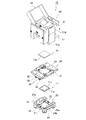
- FIG. 1 is a perspective view schematically showing a state in which two types of electrical components are simultaneously evaluated using a lower contact module and an upper contact module in the electrical component socket according to Embodiment 1 of the present invention. It is a figure which shows the state in which the module and the upper side contact module were attached to the cover. 1 is a perspective view schematically showing a state in which two types of electrical components are simultaneously evaluated using a lower contact module and an upper contact module in the electrical component socket according to Embodiment 1 of the present invention. It is a figure which shows the state from which the module and the upper side contact module were removed from the cover. It is a top view which shows roughly the socket for electrical components of FIG.
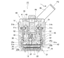
- FIG. 3 is a cross-sectional view of the electrical component socket of FIG.
- FIG. 3 is a cross-sectional view of the electrical component socket of FIG. 2 taken along line AA.
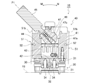
- FIG. 3 is a cross-sectional view of the electrical component socket of FIG. 2 taken along line BB, showing a state before evaluation of the electrical component.
- FIG. 3 is a cross-sectional view taken along the line BB of the electrical component socket of FIG. 2 and shows a state during evaluation of the electrical component.
- FIG. 3 is a cross-sectional view taken along line CC of the electrical component socket of FIG. 2. It is a top view which shows the upper side contact module of the socket for electrical components of FIG.
- FIG. 7 is a cross-sectional view taken along line DD of the upper contact module of FIG. 6 and shows a state where the contact unit is raised.
- FIG. 7 is a cross-sectional view taken along line DD of the upper contact module of FIG.
- FIG. 6 shows a state where the contact unit is lowered.
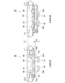
- FIG. 7 is a cross-sectional view taken along line EE of the upper contact module of FIG. 6 and compares the state in which the contact unit is raised and the state in which the contact unit is lowered.
- It is a front view which shows the processor accommodated in the contact unit of the lower contact module of the socket for electrical components shown in FIG.
- It is a bottom view which shows the processor accommodated in the contact unit of the lower contact module of the socket for electrical components shown in FIG.
- It is a front view which shows the memory accommodated in the contact unit of the upper side contact module of the socket for electrical components shown in FIG.
- FIG. is a bottom view which shows the memory accommodated in the contact unit of the upper side contact module of the socket for electrical components shown in FIG.
- Embodiment 1 of the Invention 1A to 10B show Embodiment 1 of the present invention.
- the IC socket 10 as the “electrical component socket” according to the first embodiment is of a so-called double latch type, and as shown in FIG. 1B, the processor 11 as the “lower electric component” is placed on the lower side.
- the lower contact module 20 and the upper contact module 30 are stacked in the height direction in a state where the memory 12 as the “upper electrical component” is accommodated in the upper contact module 30 while being accommodated in the contact module 20.
- the lower contact module 20 After attaching to the lower side of the shape-shaped cover 40, as shown in FIG. 4A, the lower contact module 20 is disposed on the wiring board 19, so that two types of electrical components (processor 11 and memory 12) can be simultaneously attached. It is configured so that it can be evaluated.
- the cover 40 has a cover body 41 having a substantially rectangular parallelepiped frame shape, and an elevating block 39 is movable up and down inside the cover body 41. It is installed.
- a pressing member 42 is fixedly attached to the lower side of the lifting block 39, and a heat sink 43 is integrally provided on the pressing member 42.
- the elevating block 39, the pressing member 42, and the heat sink 43 are attached so as to be movable up and down while being elastically biased upward by a spring 48.
- a substantially flat plate 44 is horizontally mounted on the upper side of the heat sink 43, as shown in FIGS. 4A to 5, a substantially flat plate 44 is horizontally mounted. Further, a substantially U-shaped operation lever 45 is attached to the cover body 41 so as to be rotatable about 90 ° in the directions of arrows M and N about the shaft 46 between the standby position P1 and the evaluation position P2. A plate cam 47 is attached to each end of the operation lever 45. When the operation lever 45 is positioned at the standby position P1, the first surface 47a of the plate cam 47 comes into contact with the upper surface of the plate 44, and the pressing member 42 is positioned at the predetermined standby height H1. On the other hand, when the operation lever 45 is positioned at the evaluation position P2, the second surface 47b of the plate cam 47 comes into contact with the upper surface of the plate 44, and the pressing member 42 is positioned at a predetermined pressing height H2.
- a pair of latches 51 on one opposite two sides can be opened and closed by rotating in the directions of arrows K and L around the shaft 52, respectively, on the outer peripheral surface of the cover body 41. Is attached.
- Each latch 51 has an operation portion 51b formed at the upper end and a tapered claw portion 51a formed inward at the lower end.
- two coil springs 53 are contracted between the operation unit 51 b at the upper end of each latch 51 and the cover body 41, so that the latch 51 is always in the direction of the arrow L (that is, The latch 51 is elastically biased in the closing direction.
- a pair of substantially cylindrical lock pins 49 for locking the lift block 39 with the pair of latches 51 closed is horizontally outward (that is, a pair of Embedded in a state protruding from the latch 51 side.
- the lower contact module 20 has a module body 21 having a substantially square frame shape as shown in FIG. 1B.
- a substantially square plate-like contact unit 22 is fitted in the center of the module body 21.
- the contact unit 22 is provided with an electric component accommodating portion 23 in an upwardly elastically biased state at an upper portion thereof so as to be movable up and down, and a number of contact pins below the electric component accommodating portion 23. (Not shown) are arranged in the vertical direction.
- these contact pins have a processor whose upper end portion is on the electrical component accommodating portion 23 of the lower contact module 20 when the lower contact module 20 and the upper contact module 30 are attached to the cover 40. 11 and the lower end portion is provided so as to contact the wiring substrate 19.
- each engaged piece 25 has a tapered upper engaged portion 25a and a tapered lower engaged portion 25b. Both the upper engaged portion 25a and the lower engaged portion 25b are formed outward so as to face the claw portions 51a of the latches 51 of the cover 40.
- the upper contact module 30 has a module body 31 having a substantially rectangular frame shape.
- a substantially square plate-like contact unit 32 is fitted to the central portion of the module body 31 so as to be movable up and down by a predetermined stroke S1 (see FIG. 8) while being elastically biased upward. That is, as shown in FIGS. 6 to 8, four substantially cylindrical guide pins 34 are attached to the module main body 31 so as to protrude downward.
- a contact unit 32 is fitted to the support pillars 34a of the guide pins 34 so as to be movable up and down. Between the flanges 34b of the guide pins 34 and the contact units 32, “biasing members" are provided. The coil spring 35 is contracted. Therefore, the upper contact module 30 is attached to the module main body 31 so as to be movable up and down in a state where the contact unit 32 is elastically urged upward by the four coil springs 35.
- the contact unit 32 is provided with an electric component accommodating portion 33 on its upper portion so as to be movable up and down while being elastically biased upward.
- a large number of contact pins (not shown) are arranged below the electrical component housing portion 33 in the vertical direction. As shown in FIG. 1A, these contact pins have a memory 12 on the electrical component accommodating portion 33 of the upper contact module 30 when the lower contact module 20 and the upper contact module 30 are attached to the cover 40.
- the lower end of the lower contact module 20 is provided so as to come into contact with the processor 11 on the electrical component housing part 23.
- four guides 36 are erected on the upper surface of the contact unit 32 so as to surround the electric component housing portion 33.
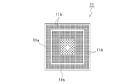
- the processor 11 and the memory 12 are both formed in a shape that can support simultaneous evaluation of two types of electrical components by the IC socket 10. That is, the processor 11 has a square plate-shaped package substrate 11a as shown in FIG. 1B, FIG. 9A, and FIG. 9B, and the package substrate 11a has a large number of needle-like leads 11b facing downward. In addition to being projecting, a large number of circular plate-like terminals 11c are provided on the surface, and the leads 11b and the terminals 11c are electrically connected in a one-to-one relationship. Further, as shown in FIG. 1B, FIG. 10A, and FIG.
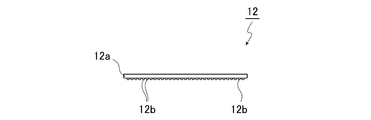
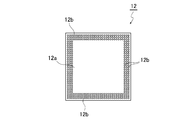
- the memory 12 has a square plate-like package substrate 12a, and the package substrate 12a has a large number of needle-like leads 12b facing downward. Projected. Therefore, when the processor 11 is accommodated in the lower contact module 20 and the memory 12 is accommodated in the upper contact module 30 and the lower contact module 20 is attached to the cover 40 via the upper contact module 30, the processor 11 The terminal 11 c and the lead 12 b of the memory 12 are electrically connected to each other via the contact pin of the upper contact module 30.
- the IC socket 10 may be used in a state where the memory 12 is accommodated in the contact unit 32 of the upper contact module 30 and the upper contact module 30 is attached to the lower side of the cover 40. In this state, the memory 12 on the contact unit 32 of the upper contact module 30 is configured to be urged by the four coil springs 35 and to contact the pressing member 42 of the cover 40.
- the processor 11 may be accommodated in the contact unit 22 of the lower contact module 20, and the memory 12 may be accommodated in the contact unit 32 of the upper contact module 30.
- the lower contact module 20 and the upper contact module 30 are used while being stacked in the height direction and attached to the lower side of the cover 40.
- the pressing member 42 presses the memory 12 on the contact unit 32 of the upper contact module 30
- the contact unit 32 of the upper contact module 30 descends with respect to the module main body 31 of the upper contact module 30, and this
- the memory 12 on the contact unit 32 is electrically connected to the processor 11 on the contact unit 22 of the lower contact module 20 via the contact pins of the contact unit 32.
- the processor 11 is accommodated on the electrical component accommodating portion 23 of the contact unit 22 of the lower contact module 20, and the memory is stored on the electrical component accommodating portion 33 of the contact unit 32 of the upper contact module 30. 12 is accommodated.
- the lower contact module 20 and the upper contact module 30 are stacked in the height direction and attached to the lower side of the cover 40.
- the cover 51 is opened with the operation part 51 b of the latch 51 of the cover 40 being pressed to open the latch 51.
- the force to push the operating portion 51b of the latch 51 is released, and the latch 51 is closed.
- the latch 51 is hooked and engaged with the upper engaged portion 25a of the engaged piece 25 of the lower contact module 20, and the lower contact module 20 and the upper contact module 30 are stacked in the height direction to cover the cover. 40 is attached to the lower side.
- the operation lever 45 of the cover 40 is rotated in the direction of arrow N to be positioned at the evaluation position P2.
- the second surface 47b of the plate cam 47 comes into contact with the upper surface of the plate 44, and the pressing member 42 is pushed down from the standby height H1 to the pressing height H2 (see FIG. 4B).
- the memory 12 on the electrical component accommodating portion 33 of the contact unit 32 of the upper contact module 30 is pushed down by the pressing member 42 with respect to the module main body 31 together with the contact unit 32, and the module of the lower contact module 20.
- the processor 11 in the main body 21 is contacted.
- the lead 12b of the memory 12 contacts and is electrically connected to the terminal 11c of the processor 11 with a predetermined contact pressure
- the lead 11b of the processor 11 contacts and electrically connects to the wiring board 19 with a predetermined contact pressure. Connected to.
- the elevating block 39 is also lowered, so that the pair of lock pins 49 are lowered to contact the stepped portions 51 c of the pair of latches 51. .
- the latch 51 can be kept closed.
- the processor 11 and the memory 12 are formed in a shape that can be used for simultaneous evaluation of two types of electrical components by the IC socket 10, so that the processor 11 and the memory 12 are connected in the double latch system. Can be evaluated at the same time.
- the heat sink 43 is provided on the cover 40 as described above, the heat generated in the processor 11 and the memory 12 due to energization is dissipated by the heat sink 43 to evaluate these two types of electrical components. It can continue without hindrance.
- the pair of latches 51 holding the lower contact module 20 are held closed by the pair of lock pins 49, so that an external force that opens the latch 51 is applied.
- the lower contact module 20 and the upper contact module 30 can be securely gripped until the evaluation of the electrical components is completed.
- the upper contact module 30 is placed on the lower contact module 20, and finally the cover 40 is placed on the upper contact module 30.
- the lower contact module 20 and the upper contact module 30 may be attached to the cover 40.
- the latch 51 of the cover 40 has a tapered claw portion 51a
- the engaged piece 25 of the lower contact module 20 has a tapered upper engaged portion 25a.
- the lower contact module 20 and the upper contact module 30 can be easily attached to the cover 40 simply by pressing the cover 40 down to the lower contact module 20 side.
- the processor 11 is accommodated in the contact unit 22 of the lower contact module 20, and the memory 12 is accommodated in the contact unit 32 of the upper contact module 30.
- the pressing member 42 corresponds to the lowering operation.
- the contact unit 32 of the upper contact module 30 is lowered.
- the pressing force of the pressing member 42 can be transmitted to the contact unit 22 of the lower contact module 20 via the contact unit 32 of the upper contact module 30. Therefore, in the so-called double latch type IC socket 10, it is possible to prevent the occurrence of pressing failure of the memory 12 (excessive or insufficient pressing amount, etc.).
- the memory 12 on the contact unit 32 of the upper contact module 30 is always attached to the pressing member 42. It comes into contact. For this reason, there is no gap between the memory 12 and the pressing member 42. As a result, it is possible to prevent the occurrence of poor seating of the memory 12 in the so-called double latch type IC socket 10.
- the present invention is applied to the IC socket 10 as the “electrical component socket”, but it is needless to say that the present invention can be applied to other devices.
Landscapes
- Physics & Mathematics (AREA)
- General Physics & Mathematics (AREA)
- Connecting Device With Holders (AREA)
- Testing Of Individual Semiconductor Devices (AREA)
Abstract
【課題】ダブルラッチ方式の電気部品用ソケットにおいて、電気部品の押圧不良および着座不良の発生を未然に防ぐ。【解決手段】この電気部品用ソケットでは、下側コンタクトモジュール(20)の下側コンタクトユニット(22)に下側電気部品(11)が収容されているとともに、上側コンタクトモジュール(30)の上側コンタクトユニット(32)に上側電気部品(12)が収容されている。下側コンタクトモジュール(20)および上側コンタクトモジュール(30)は、上下方向に配置されて、カバー(40)の下側に取り付けられている。押圧部材が上側コンタクトユニット(32)上の上側電気部品(12)を押圧したときには、上側コンタクトユニット(32)が上側モジュール本体(31)に対して下降する。そして、上側コンタクトユニット(32)上の上側電気部品(12)が下側コンタクトユニット(22)上の下側電気部品(11)に導通する。
Description
本発明は、例えば、プロセッサ、メモリ等の電気部品を評価する際に用いられる電気部品用ソケットに関するものである。
従来、この種の電気部品用ソケットとしては、電気部品(例えば、半導体デバイス、電子部品パッケージなど)を収容するコンタクトモジュール(例えば、ソケット本体など)の上側に、カバー(例えば、蓋体、蓋など)が爪係合方式で着脱自在に取り付けられた構造を有するものが提案されている(例えば、特許文献1、2参照)。
この電気部品用ソケットでは、コンタクトモジュールに電気部品を収容した後、このコンタクトモジュールにカバーを爪係合方式でロックすることにより、コンタクトモジュールに配設されたコンタクトピンに電気部品の端子を所定の接圧で接触させて、この電気部品を評価することができるようになっている。
ところで、このような構造を有する電気部品用ソケットを用いて、2種類の電気部品(例えば、プロセッサとメモリ)を同時に評価する場合には、いわゆるダブルラッチ方式を採用することが考えられる。このダブルラッチ方式では、2種類の電気部品の評価に先立ち、カバーおよび2種類のコンタクトモジュール(下側コンタクトモジュールおよび上側コンタクトモジュール)を用意し、一方の電気部品(例えば、プロセッサ)を下側コンタクトモジュールのコンタクトユニットに収容するとともに、他方の電気部品(例えば、メモリ)を上側コンタクトモジュールのコンタクトユニットに収容する。次いで、下側コンタクトモジュールおよび上側コンタクトモジュールを高さ方向(上下方向)に積み上げてカバーの下側に取り付ける。この状態で、配線基板上に下側コンタクトモジュールを配設し、カバーの押圧部材で上側コンタクトモジュールを下向き(下側コンタクトモジュール側)に押圧する。
しかしながら、この上側コンタクトモジュールにおいては、電気部品を収容するコンタクトユニットがモジュール本体に対して高さ方向に固定されているため、次のような不都合が生じる。
第1に、下側コンタクトモジュールに対する上側コンタクトモジュールの積み上げ状況によっては、押圧部材による電気部品の押し込み量の過不足などの押圧不良が発生する場合がある。例えば、下側コンタクトモジュールおよび上側コンタクトモジュールにそれぞれ電気部品を収容し、これらの下側コンタクトモジュールおよび上側コンタクトモジュールを高さ方向に積み上げてカバーの下側に取り付けたときに、上側コンタクトモジュールのモジュール本体が下側コンタクトモジュールのモジュール本体に接触して下降動作を阻止されていると、押圧部材が下降しても上側コンタクトモジュールのモジュール本体およびコンタクトユニットが下降しないため、上側コンタクトモジュールのコンタクトユニットに収容された電気部品の押し込み量が過剰になる一方、下側コンタクトモジュールのコンタクトユニットに収容された電気部品の押し込み量が不足する。
第2に、下側コンタクトモジュールおよび上側コンタクトモジュールにそれぞれ電気部品を収容し、これらの下側コンタクトモジュールおよび上側コンタクトモジュールを高さ方向に積み上げてカバーの下側に取り付けたときに、上側コンタクトモジュールのコンタクトユニット上の電気部品と押圧部材との間に隙間があると、この電気部品用ソケットの取り扱い中に上側コンタクトモジュールのコンタクトユニットから電気部品が浮き上がってしまい、電気部品の着座不良が発生する恐れがある。
そこで、この発明は、いわゆるダブルラッチ方式において、電気部品の押圧不良および着座不良の発生を未然に防ぐことが可能な電気部品用ソケットを提供することを課題としている。
かかる課題を達成するために、本発明は、下側電気部品が収容される下側コンタクトユニットを備える下側コンタクトモジュールと、上側電気部品が収容される上側コンタクトユニットと、上端が該上側電気部品の端子に接触すると共に下端が該上側コンタクトユニットから下方に突出したコンタクトピンと、該上側コンタクトユニットを上下動自在に支持する上側モジュール本体とを有する上側コンタクトモジュールと、前記下側電気部品が収容された前記下側コンタクトモジュールと、前記下側電気部品が収容される前記下側コンタクトモジュールと前記上側電気部品が収容される前記上側コンタクトモジュールとを上下方向に配置した状態で収容するカバーと、前記上側コンタクトモジュールに収容された前記上側電気部品の上面を下向きに押圧することにより前記上側コンタクトユニットを下降させ、これにより、該上側コンタクトユニットから下方に突出した前記コンタクトピンを、前記下側コンタクトモジュールに収容された前記下側電気部品と導通させるために、該カバーに取り付けられた前記押圧部材とを有することを特徴とする。
本発明においては、前記上側コンタクトモジュールの前記上側コンタクトユニットは、当該上側コンタクトモジュールの上側モジュール本体に対して付勢部材によって上方へ弾性的に付勢された状態で上下動自在に取り付けられており、
前記上側コンタクトモジュールの前記上側コンタクトユニットに前記上側電気部品が収容されているとともに、この上側コンタクトモジュールが前記カバーの下側に取り付けられている状態では、この上側コンタクトモジュールの前記上側コンタクトユニット上の前記上側電気部品が、前記付勢部材によって付勢されて前記押圧部材に接触するように構成されていることが望ましい。
前記上側コンタクトモジュールの前記上側コンタクトユニットに前記上側電気部品が収容されているとともに、この上側コンタクトモジュールが前記カバーの下側に取り付けられている状態では、この上側コンタクトモジュールの前記上側コンタクトユニット上の前記上側電気部品が、前記付勢部材によって付勢されて前記押圧部材に接触するように構成されていることが望ましい。
本発明によれば、上側コンタクトモジュールの上側コンタクトユニットに収容された上側電気部品を押圧部材で押圧して下降させることで、この上側コンタクトモジュールの上側コンタクトユニットを介して下側コンタクトモジュールのコンタクトユニットに押圧部材の押圧力を伝達することができる。したがって、いわゆるダブルラッチ方式の電気部品用ソケットにおいて、上側電気部品の押圧不良(押し込み量の過不足など)の発生を未然に防ぐことが可能となる。
また、本発明において、付勢部材を用いて、上側電気部品が常に押圧部材に接触した状態にすることで、いわゆるダブルラッチ方式の電気部品用ソケットにおいて、上側電気部品の着座不良の発生を未然に防ぐことが可能となる。
以下、本発明の実施の形態について説明する。
[発明の実施の形態1]
図1A乃至図10Bには、本発明の実施の形態1を示す。
図1A乃至図10Bには、本発明の実施の形態1を示す。
この実施の形態1に係る「電気部品用ソケット」としてのICソケット10は、いわゆるダブルラッチ方式のものであって、図1Bに示すように、「下側電気部品」であるプロセッサ11を下側コンタクトモジュール20に収容するとともに、「上側電気部品」であるメモリ12を上側コンタクトモジュール30に収容した状態で、これらの下側コンタクトモジュール20および上側コンタクトモジュール30を高さ方向に積み上げて平面視四角形状のカバー40の下側に取り付けた後、図4Aに示すように、配線基板19上に下側コンタクトモジュール20を配設することにより、2種類の電気部品(プロセッサ11およびメモリ12)を同時に評価できるように構成されたものである。
ここで、カバー40は、図1B、図4A、図4B等に示すように、略直方体枠形状のカバー本体41を有しており、カバー本体41の内部には昇降ブロック39が上下動自在に装着されている。昇降ブロック39の下側には押圧部材42が固定して取り付けられており、押圧部材42にはヒートシンク43が一体に設けられている。そして、これらの昇降ブロック39、押圧部材42およびヒートシンク43は、スプリング48によって上方へ弾性的に付勢された状態で上下動自在に取り付けられている。
また、ヒートシンク43の上側には、図4A乃至図5に示すように、略平板状のプレート44が水平に搭載されている。さらに、カバー本体41には、略U字形の操作レバー45が、待機位置P1と評価位置P2との間で軸46を中心として矢印M、N方向に約90°回動自在に取り付けられており、操作レバー45の各端部にはそれぞれ板カム47が装着されている。そして、操作レバー45が待機位置P1に位置決めされると、板カム47の第1面47aがプレート44の上面に接触し、押圧部材42が所定の待機高さH1に位置決めされた状態になる。一方、操作レバー45が評価位置P2に位置決めされると、板カム47の第2面47bがプレート44の上面に接触し、押圧部材42が所定の押圧高さH2に位置決めされた状態になる。
また、カバー本体41の外周面には、図4Aに示すように、一方の対向2辺に一対のラッチ51が、それぞれシャフト52を中心として矢印K、L方向に回転することによって開閉しうるように取り付けられている。各ラッチ51にはそれぞれ、上端部に操作部51bが形成されているとともに、下端部にテーパ状の爪部51aが内向きに形成されている。図2に示すように、各ラッチ51の上端部の操作部51bとカバー本体41との間にはそれぞれ、2個のコイルスプリング53が縮設されて、ラッチ51を常に矢印L方向(すなわち、ラッチ51が閉じる方向)に弾性的に付勢している。さらに、昇降ブロック39には、図4A、図4Bに示すように、一対のラッチ51が閉じた状態でロックするための一対の略円柱状のロックピン49が、水平方向外向き(つまり、一対のラッチ51側)に突出した状態で埋設されている。
また、下側コンタクトモジュール20は、図1Bに示すように、略正方形枠状のモジュール本体21を有している。モジュール本体21の中央部には、略正方形板状のコンタクトユニット22が嵌合している。このコンタクトユニット22には、その上部に電気部品収容部23が上方に弾性的に付勢された状態で上下動自在に設けられているとともに、この電気部品収容部23の下方に多数のコンタクトピン(図示せず)が上下方向に配設されている。これらのコンタクトピンは、図1Aに示すように、下側コンタクトモジュール20および上側コンタクトモジュール30がカバー40に取り付けられた状態では、上端部が下側コンタクトモジュール20の電気部品収容部23上のプロセッサ11に接触するとともに、下端部が配線基板19に接触するように設けられている。
さらに、モジュール本体21の外周面には、図1B、図4等に示すように、カバー40の一対のラッチ51と係合しうる一対の被係合片25が設けられている。各被係合片25はそれぞれ、テーパ状の上側被係合部25aおよびテーパ状の下側被係合部25bを有している。これらの上側被係合部25a、下側被係合部25bはいずれも、カバー40の各ラッチ51の爪部51aに対向して外向きに形成されている。
一方、上側コンタクトモジュール30は、図1Bに示すように、略長方形枠状のモジュール本体31を有している。モジュール本体31の中央部には、略正方形板状のコンタクトユニット32が上方へ弾性的に付勢された状態で所定のストロークS1(図8参照)だけ上下動自在に嵌合している。すなわち、モジュール本体31には、図6乃至図8に示すように、4本の略円柱状のガイドピン34が下方へ突出する状態で取り付けられている。これらのガイドピン34の支柱部34aにはコンタクトユニット32が上下動自在に嵌合しており、各ガイドピン34のフランジ部34bとコンタクトユニット32との間にはそれぞれ、「付勢部材」としてのコイルスプリング35が縮設されている。そのため、上側コンタクトモジュール30は、コンタクトユニット32がモジュール本体31に対して、4本のコイルスプリング35によって上方へ弾性的に付勢された状態で、上下動自在に取り付けられている。
また、このコンタクトユニット32には、図8に示すように、その上部に電気部品収容部33が、上方に弾性的に付勢された状態で上下動自在に設けられている。また、この電気部品収容部33の下方には、多数のコンタクトピン(図示せず)が上下方向に配設されている。これらのコンタクトピンは、図1Aに示すように、下側コンタクトモジュール20および上側コンタクトモジュール30がカバー40に取り付けられた状態では、上端部が上側コンタクトモジュール30の電気部品収容部33上のメモリ12に接触するとともに、下端部が下側コンタクトモジュール20の電気部品収容部23上のプロセッサ11に接触するように設けられている。さらに、コンタクトユニット32の上面には、図6に示すように、4つのガイド36が電気部品収容部33を包囲するように立設されている。
なお、プロセッサ11およびメモリ12は、いずれも、ICソケット10による2種類の電気部品の同時評価に対応可能な形状に形成されている。すなわち、プロセッサ11は、図1Bや図9A、図9Bに示すように、正方形板状のパッケージ基板11aを有しており、パッケージ基板11aには、裏面に針状の多数のリード11bが下向きに突設されているとともに、表面に円形板状の多数の端子11cが設けられて、これらのリード11bと端子11cとが1対1で導通している。また、メモリ12は、図1Bや図10A、図10Bに示すように、正方形板状のパッケージ基板12aを有しており、パッケージ基板12aには、裏面に針状の多数のリード12bが下向きに突設されている。そのため、プロセッサ11を下側コンタクトモジュール20に収容するとともに、メモリ12を上側コンタクトモジュール30に収容した状態で、上側コンタクトモジュール30を介してカバー40に下側コンタクトモジュール20を取り付けると、プロセッサ11の端子11cとメモリ12のリード12bとが、上側コンタクトモジュール30のコンタクトピンを介して互いに電気的に接続された状態になる。
そして、ICソケット10は、上側コンタクトモジュール30のコンタクトユニット32にメモリ12が収容されるとともに、この上側コンタクトモジュール30がカバー40の下側に取り付けられる状態で使用される場合がある。この状態では、この上側コンタクトモジュール30のコンタクトユニット32上のメモリ12が、4本のコイルスプリング35によって付勢されてカバー40の押圧部材42に接触するように構成されている。
また、ICソケット10は、下側コンタクトモジュール20のコンタクトユニット22にプロセッサ11が収容されるとともに、上側コンタクトモジュール30のコンタクトユニット32にメモリ12が収容される場合がある。この場合、これらの下側コンタクトモジュール20および上側コンタクトモジュール30が、高さ方向に積み上げられて、カバー40の下側に取り付けられた状態で使用される。この状態で、押圧部材42が上側コンタクトモジュール30のコンタクトユニット32上のメモリ12を押圧したときには、上側コンタクトモジュール30のコンタクトユニット32が上側コンタクトモジュール30のモジュール本体31に対して下降して、このコンタクトユニット32上のメモリ12が、コンタクトユニット32のコンタクトピンを介して、下側コンタクトモジュール20のコンタクトユニット22上のプロセッサ11に導通する。
かかるICソケット10を用いて2種類の電気部品(プロセッサ11およびメモリ12)を同時に評価するときには、例えば次の手順に従う。
まず、図1Bに示すように、下側コンタクトモジュール20のコンタクトユニット22の電気部品収容部23上にプロセッサ11を収容するとともに、上側コンタクトモジュール30のコンタクトユニット32の電気部品収容部33上にメモリ12を収容する。次いで、図4Aに示すように、これらの下側コンタクトモジュール20および上側コンタクトモジュール30を高さ方向に積み上げてカバー40の下側に取り付ける。それには、例えば、下側コンタクトモジュール20の上側に上側コンタクトモジュール30を載置した後、カバー40のラッチ51の操作部51bを押してラッチ51を開いた状態で、このカバー40を上側コンタクトモジュール30の上側に載置してから、ラッチ51の操作部51bを押す力を解除してラッチ51を閉じる。すると、このラッチ51が下側コンタクトモジュール20の被係合片25の上側被係合部25aに引っ掛かって係合し、下側コンタクトモジュール20および上側コンタクトモジュール30が高さ方向に積み上げられてカバー40の下側に取り付けられた状態になる。
次いで、図3および図4Aに示すように、このICソケット10を配線基板19上に配設した後、カバー40の操作レバー45を矢印N方向に回動して評価位置P2に位置決めする。すると、板カム47の第2面47bがプレート44の上面に接触し、押圧部材42が待機高さH1から押圧高さH2まで押し下げられて下降する(図4B参照)。その結果、この押圧部材42に押されて上側コンタクトモジュール30のコンタクトユニット32の電気部品収容部33上のメモリ12がコンタクトユニット32とともにモジュール本体31に対して下降し、下側コンタクトモジュール20のモジュール本体21内のプロセッサ11に接触する。そして、メモリ12のリード12bがプロセッサ11の端子11cに所定の接圧で接触して電気的に接続されるとともに、プロセッサ11のリード11bが配線基板19に所定の接圧で接触して電気的に接続される。
また、こうした押圧部材42の下降動作に伴い、図4A及び図4Bに示すように、昇降ブロック39も下降するので、一対のロックピン49が下降して一対のラッチ51の段差部51cに接触する。その結果、これらのラッチ51が閉じた状態を保持することができる。
この状態で、2種類の電気部品(プロセッサ11およびメモリ12)に電流を流して評価する。
このとき、プロセッサ11およびメモリ12は、上述したとおり、ICソケット10による2種類の電気部品の同時評価に対応可能な形状に形成されているので、ダブルラッチ方式において、プロセッサ11とメモリ12とを同時に評価することができる。
また、カバー40には、上述したとおり、ヒートシンク43が設けられているので、通電に伴ってプロセッサ11およびメモリ12で発生した熱をヒートシンク43で放熱して、これら2種類の電気部品の評価を支障なく継続することができる。
さらに、下側コンタクトモジュール20を把持している一対のラッチ51は、上述したとおり、一対のロックピン49によって閉じた状態が保持されているので、たとえラッチ51を開くような外力が作用しても、電気部品の評価が終了するまで下側コンタクトモジュール20および上側コンタクトモジュール30を確実に把持することができる。
なお、ここでは、下側コンタクトモジュール20および上側コンタクトモジュール30をカバー40に取り付けてICソケット10を組み立てた後、このICソケット10を配線基板19上に配設する手順について説明したが、これ以外の手順も考えられる。
例えば、下側コンタクトモジュール20を配線基板19上に配設した後、この下側コンタクトモジュール20上に上側コンタクトモジュール30を載置し、最後に、この上側コンタクトモジュール30上にカバー40を載置し、このカバー40に下側コンタクトモジュール20および上側コンタクトモジュール30を取り付けても構わない。この場合、カバー40のラッチ51がテーパ状の爪部51aを有しているとともに、下側コンタクトモジュール20の被係合片25がテーパ状の上側被係合部25aを有しているので、カバー40を下側コンタクトモジュール20側に押し下げるだけで、カバー40に下側コンタクトモジュール20および上側コンタクトモジュール30を簡単に取り付けることができる。
このように、この実施の形態1では、下側コンタクトモジュール20のコンタクトユニット22にプロセッサ11を収容するとともに、上側コンタクトモジュール30のコンタクトユニット32にメモリ12を収容し、さらに、これらの下側コンタクトモジュール20および上側コンタクトモジュール30を高さ方向に積み上げてカバー40の下側に取り付けた状態で、上側コンタクトモジュール30のコンタクトユニット32を押圧部材42で押圧すると、この押圧部材42の下降動作に対応して上側コンタクトモジュール30のコンタクトユニット32が下降する。このため、上側コンタクトモジュール30のコンタクトユニット32を介して、下側コンタクトモジュール20のコンタクトユニット22に、押圧部材42の押圧力を伝達することができる。したがって、いわゆるダブルラッチ方式のICソケット10において、メモリ12の押圧不良(押し込み量の過不足など)の発生を未然に防ぐことが可能となる。
また、上側コンタクトモジュール30のコンタクトユニット32にメモリ12を収容し、この上側コンタクトモジュール30をカバー40の下側に取り付けると、上側コンタクトモジュール30のコンタクトユニット32上のメモリ12が常に押圧部材42に接触した状態になる。このため、このメモリ12と押圧部材42との間に、隙間が生じなくなる。その結果、いわゆるダブルラッチ方式のICソケット10において、メモリ12の着座不良の発生を未然に防ぐことが可能となる。
[発明のその他の実施の形態]
なお、上述した実施の形態1では、4本のガイドピン34およびコイルスプリング35を用いた機構により、コンタクトユニット32がモジュール本体31に対して上方へ弾性的に付勢された状態で上下動自在に取り付けられている上側コンタクトモジュール30について説明したが、これ以外の機構を代用または併用することもできる。
なお、上述した実施の形態1では、4本のガイドピン34およびコイルスプリング35を用いた機構により、コンタクトユニット32がモジュール本体31に対して上方へ弾性的に付勢された状態で上下動自在に取り付けられている上側コンタクトモジュール30について説明したが、これ以外の機構を代用または併用することもできる。
また、上述した実施の形態1では、ICソケット10の下側コンタクトモジュール20、上側コンタクトモジュール30に収容する電気部品として、それぞれプロセッサ11、メモリ12を用いる場合について説明したが、これに限らず、例えば、下側コンタクトモジュール20と上側コンタクトモジュール30のいずれにもプロセッサを収容し、これら2個のプロセッサを同時に評価することも勿論できる。
さらに、上述した実施の形態1では、「電気部品用ソケット」としてのICソケット10に本発明を適用したが、これに限らず、他の装置にも適用できることは勿論である。
10……ICソケット(電気部品用ソケット)
11……プロセッサ(下側電気部品)
12……メモリ(上側電気部品)
20……下側コンタクトモジュール
21……モジュール本体
22……コンタクトユニット
30……上側コンタクトモジュール
31……モジュール本体
32……コンタクトユニット
35……コイルスプリング(付勢部材)
40……カバー
42……押圧部材
11……プロセッサ(下側電気部品)
12……メモリ(上側電気部品)
20……下側コンタクトモジュール
21……モジュール本体
22……コンタクトユニット
30……上側コンタクトモジュール
31……モジュール本体
32……コンタクトユニット
35……コイルスプリング(付勢部材)
40……カバー
42……押圧部材
Claims (2)
- 下側電気部品が収容される下側コンタクトユニットを備える下側コンタクトモジュールと、
上側電気部品が収容される上側コンタクトユニットと、上端が該上側電気部品の端子に接触すると共に下端が該上側コンタクトユニットから下方に突出したコンタクトピンと、該上側コンタクトユニットを上下動自在に支持する上側モジュール本体とを有する上側コンタクトモジュールと、
前記下側電気部品が収容される前記下側コンタクトモジュールと、前記上側電気部品が収容される前記上側コンタクトモジュールとを、上下方向に配置した状態で収容するカバーと、
前記上側コンタクトモジュールに収容された前記上側電気部品の上面を下向きに押圧することにより前記上側コンタクトユニットを下降させ、これにより、該上側コンタクトユニットから下方に突出した前記コンタクトピンを、前記下側コンタクトモジュールに収容された前記下側電気部品と導通させるために、該カバーに取り付けられた前記押圧部材と、
を有することを特徴とする電気部品用ソケット。 - 前記上側コンタクトモジュールの前記上側コンタクトユニットは、当該上側コンタクトモジュールの上側モジュール本体に対して付勢部材によって上方へ弾性的に付勢された状態で上下動自在に取り付けられており、
前記上側コンタクトモジュールの前記上側コンタクトユニットに前記上側電気部品が収容されているとともに、この上側コンタクトモジュールが前記カバーの下側に取り付けられている状態では、この上側コンタクトモジュールの前記上側コンタクトユニット上の前記上側電気部品が、前記付勢部材によって付勢されて前記押圧部材に接触するように構成されていることを特徴とする請求項1に記載の電気部品用ソケット。
Applications Claiming Priority (2)
| Application Number | Priority Date | Filing Date | Title |
|---|---|---|---|
| JP2016039977A JP6621343B2 (ja) | 2016-03-02 | 2016-03-02 | 電気部品用ソケット |
| JP2016-039977 | 2016-03-02 |
Publications (1)
| Publication Number | Publication Date |
|---|---|
| WO2017150436A1 true WO2017150436A1 (ja) | 2017-09-08 |
Family
ID=59743924
Family Applications (1)
| Application Number | Title | Priority Date | Filing Date |
|---|---|---|---|
| PCT/JP2017/007443 Ceased WO2017150436A1 (ja) | 2016-03-02 | 2017-02-27 | 電気部品用ソケット |
Country Status (2)
| Country | Link |
|---|---|
| JP (1) | JP6621343B2 (ja) |
| WO (1) | WO2017150436A1 (ja) |
Citations (5)
| Publication number | Priority date | Publication date | Assignee | Title |
|---|---|---|---|---|
| JP2008020458A (ja) * | 2006-07-13 | 2008-01-31 | Samsung Electronics Co Ltd | パッケージテスト用ソケット、テストソケット用ラバー及びテストソケット用ガイド |
| US7484968B2 (en) * | 2006-01-25 | 2009-02-03 | Samsung Electronics Co., Ltd. | Socket for an electrical tester |
| JP2009038192A (ja) * | 2007-08-01 | 2009-02-19 | Alps Electric Co Ltd | 半導体装置の製造方法およびインターポーザ |
| JP2015046265A (ja) * | 2013-08-27 | 2015-03-12 | 三菱電機株式会社 | 半導体ソケット及び半導体モジュール |
| JP2015195102A (ja) * | 2014-03-31 | 2015-11-05 | 株式会社エンプラス | ラッチ機構及び電気部品用ソケット |
-
2016
- 2016-03-02 JP JP2016039977A patent/JP6621343B2/ja not_active Expired - Fee Related
-
2017
- 2017-02-27 WO PCT/JP2017/007443 patent/WO2017150436A1/ja not_active Ceased
Patent Citations (5)
| Publication number | Priority date | Publication date | Assignee | Title |
|---|---|---|---|---|
| US7484968B2 (en) * | 2006-01-25 | 2009-02-03 | Samsung Electronics Co., Ltd. | Socket for an electrical tester |
| JP2008020458A (ja) * | 2006-07-13 | 2008-01-31 | Samsung Electronics Co Ltd | パッケージテスト用ソケット、テストソケット用ラバー及びテストソケット用ガイド |
| JP2009038192A (ja) * | 2007-08-01 | 2009-02-19 | Alps Electric Co Ltd | 半導体装置の製造方法およびインターポーザ |
| JP2015046265A (ja) * | 2013-08-27 | 2015-03-12 | 三菱電機株式会社 | 半導体ソケット及び半導体モジュール |
| JP2015195102A (ja) * | 2014-03-31 | 2015-11-05 | 株式会社エンプラス | ラッチ機構及び電気部品用ソケット |
Also Published As
| Publication number | Publication date |
|---|---|
| JP6621343B2 (ja) | 2019-12-18 |
| JP2017156227A (ja) | 2017-09-07 |
Similar Documents
| Publication | Publication Date | Title |
|---|---|---|
| JP5612436B2 (ja) | 電気部品用ソケット | |
| JP5530312B2 (ja) | 電気部品用ソケット | |
| US7393232B2 (en) | Socket for electrical parts | |
| KR101593634B1 (ko) | 전기적 검사소켓 | |
| US7097488B2 (en) | Socket for electrical parts | |
| JP2015115151A (ja) | ソケット | |
| JP2006294308A (ja) | 電気部品用ソケット | |
| KR20120015013A (ko) | 테스트핸들러용 인서트 | |
| JP6621343B2 (ja) | 電気部品用ソケット | |
| JP6604813B2 (ja) | 電気部品用ソケット | |
| KR101585272B1 (ko) | 인서트의 래치 개방 장치 | |
| TWI683488B (zh) | 電氣零件用插座 | |
| JP2017219413A (ja) | 電気部品用ソケット | |
| KR102362735B1 (ko) | 전기 부품용 소켓 | |
| WO2017138522A1 (ja) | 電気部品用ソケット | |
| US12099077B2 (en) | Socket | |
| JP2003303655A (ja) | 電気部品用ソケット | |
| JP2018026268A (ja) | 電気部品用ソケット | |
| JP5627449B2 (ja) | 電気部品用ソケット | |
| KR100570200B1 (ko) | 반도체 소자 테스트 핸들러용 캐리어 모듈 | |
| TWM374666U (en) | Electrical connector | |
| JP2012212623A (ja) | 電気部品用ソケット | |
| JP6192530B2 (ja) | 電気部品用ソケット | |
| KR200379637Y1 (ko) | 반도체칩캐리어 | |
| JP2012155859A (ja) | 電気部品用ソケット |
Legal Events
| Date | Code | Title | Description |
|---|---|---|---|
| NENP | Non-entry into the national phase |
Ref country code: DE |
|
| 121 | Ep: the epo has been informed by wipo that ep was designated in this application |
Ref document number: 17759902 Country of ref document: EP Kind code of ref document: A1 |
|
| 122 | Ep: pct application non-entry in european phase |
Ref document number: 17759902 Country of ref document: EP Kind code of ref document: A1 |