WO2017150078A1 - 電界イメージング装置 - Google Patents
電界イメージング装置 Download PDFInfo
- Publication number
- WO2017150078A1 WO2017150078A1 PCT/JP2017/004151 JP2017004151W WO2017150078A1 WO 2017150078 A1 WO2017150078 A1 WO 2017150078A1 JP 2017004151 W JP2017004151 W JP 2017004151W WO 2017150078 A1 WO2017150078 A1 WO 2017150078A1
- Authority
- WO
- WIPO (PCT)
- Prior art keywords
- frequency
- signal
- electric field
- field imaging
- imaging apparatus
- Prior art date
- Legal status (The legal status is an assumption and is not a legal conclusion. Google has not performed a legal analysis and makes no representation as to the accuracy of the status listed.)
- Ceased
Links
Images


Classifications
-
- H—ELECTRICITY
- H10—SEMICONDUCTOR DEVICES; ELECTRIC SOLID-STATE DEVICES NOT OTHERWISE PROVIDED FOR
- H10F—INORGANIC SEMICONDUCTOR DEVICES SENSITIVE TO INFRARED RADIATION, LIGHT, ELECTROMAGNETIC RADIATION OF SHORTER WAVELENGTH OR CORPUSCULAR RADIATION
- H10F39/00—Integrated devices, or assemblies of multiple devices, comprising at least one element covered by group H10F30/00, e.g. radiation detectors comprising photodiode arrays
- H10F39/80—Constructional details of image sensors
- H10F39/806—Optical elements or arrangements associated with the image sensors
-
- G—PHYSICS
- G01—MEASURING; TESTING
- G01R—MEASURING ELECTRIC VARIABLES; MEASURING MAGNETIC VARIABLES
- G01R29/00—Arrangements for measuring or indicating electric quantities not covered by groups G01R19/00 - G01R27/00
- G01R29/08—Measuring electromagnetic field characteristics
-
- G—PHYSICS
- G02—OPTICS
- G02B—OPTICAL ELEMENTS, SYSTEMS OR APPARATUS
- G02B5/00—Optical elements other than lenses
- G02B5/30—Polarising elements
- G02B5/3025—Polarisers, i.e. arrangements capable of producing a definite output polarisation state from an unpolarised input state
-
- G—PHYSICS
- G02—OPTICS
- G02F—OPTICAL DEVICES OR ARRANGEMENTS FOR THE CONTROL OF LIGHT BY MODIFICATION OF THE OPTICAL PROPERTIES OF THE MEDIA OF THE ELEMENTS INVOLVED THEREIN; NON-LINEAR OPTICS; FREQUENCY-CHANGING OF LIGHT; OPTICAL LOGIC ELEMENTS; OPTICAL ANALOGUE/DIGITAL CONVERTERS
- G02F1/00—Devices or arrangements for the control of the intensity, colour, phase, polarisation or direction of light arriving from an independent light source, e.g. switching, gating or modulating; Non-linear optics
- G02F1/0009—Materials therefor
- G02F1/0018—Electro-optical materials
-
- H—ELECTRICITY
- H04—ELECTRIC COMMUNICATION TECHNIQUE
- H04N—PICTORIAL COMMUNICATION, e.g. TELEVISION
- H04N23/00—Cameras or camera modules comprising electronic image sensors; Control thereof
- H04N23/56—Cameras or camera modules comprising electronic image sensors; Control thereof provided with illuminating means
-
- H—ELECTRICITY
- H10—SEMICONDUCTOR DEVICES; ELECTRIC SOLID-STATE DEVICES NOT OTHERWISE PROVIDED FOR
- H10W—GENERIC PACKAGES, INTERCONNECTIONS, CONNECTORS OR OTHER CONSTRUCTIONAL DETAILS OF DEVICES COVERED BY CLASS H10
- H10W90/00—Package configurations
Definitions
- the present invention relates to an electric field imaging apparatus capable of visualizing a two-dimensional distribution of a high-frequency oscillating electric field and its temporal and spatial changes in real time.
- Non-patent Document 1 reported by the National Institute of Information and Communications Technology is known as one that visualizes the two-dimensional distribution of the high-frequency electric field in real time. This is based on the electromagnetic field high-speed imaging device described in 1 and the subsequent improvements.
- This electric field camera is a device that captures and displays the electric field distribution in the microwave band up to 100 GHz in real time by superimposing the super parallelism and ultra high speed of light through the electro-optic effect.
- FIG. 1A shows a block diagram of the electric field camera
- the driver unit includes an f LO oscillation unit for a blinking light source and an f RF oscillation unit for a specimen.
- the frequency emitted from the specimen (DUT) when the electro-optic (EO) crystal plate (probe in Patent Document 1) is irradiated as illumination light with polarized light whose amplitude is modulated at a frequency f LO from a blinking light source.
- the polarization plane of the illumination light is given a change reflecting the change in birefringence at each position.
- polarized light whose polarization plane has been changed is selected by an optical system including an analyzer, and this two-dimensional distribution is imaged by an image sensor.
- the signals for each pixel of the image sensor are obtained in parallel. This signal is sequentially output for each pixel, and is displayed on the image display device after arithmetic processing by the image processing device.
- the high-frequency electrical signal to be imaged and the sampling of the high-speed CMOS image sensor (IS) inside the imaging system are synchronized with each other. This is to avoid instability and disappearance in the display of the result of batch frequency conversion performed in each pixel of the image sensor.
- each signal source for the frequency f LO and the frequency f RF can be synchronized with a reference signal from an external signal source.
- IS is a master
- DUT operation is a slave. That is, conventionally, electric field imaging has been performed by a system in a synchronous mode and a master mode.
- the signal source for the frequency f LO (LO signal source) is also synchronized with the IS reference signal.
- the difference frequency component ⁇ f with the RF signal needs to be synchronized with the timing of IS sampling.
- the band of the difference frequency component ⁇ f is restricted to a moving image frame rate (typically 10 Hz) or less, but in order to realize this, when the instantaneous frequency of the RF signal fluctuates due to modulation or data superposition, etc. , it is necessary to signal for the frequency f LO so as to maintain the frequency difference ⁇ f between the signal and the RF signal for the frequency f LO follows the RF signals, D Restrictions were placed on both the UT and LO signal sources.
- the specimens that can be observed by the conventional electric field camera system are greatly limited.
- the sample is limited to a sample that can be synchronized with an external signal source (mainly a synthesizer) or a sample that has a function that can be synchronized with an IS clock.
- an external signal source mainly a synthesizer
- a sample that has a function that can be synchronized with an IS clock In general, a commercial product or a high-frequency module used in the product requires modification such as adding a circuit having a synchronization function or adding wiring for signal input / output. What could be rare was rare.
- the signal used here is synchronized with the reference signal from the IS as described above.
- the signal for the frequency f LO and the above-described signal are used.
- a frequency synthesizer has been used for each signal source for the frequency f RF .
- each bandwidth was 1 Hz or less, and the RF signal itself was extremely narrow.
- a module having an actual self-propelled signal source or a device using the same has a large fluctuation and a large bandwidth. This variation differs for each high-frequency device, but it is desirable to be able to realize a bandwidth tailored to the specimen.
- the oscillating electric field in the oscillating electromagnetic field is observed using the electro-optic effect in the EO crystal.
- the electro-optic effect is a phenomenon in which the phase state of polarized light traveling through the EO crystal changes.
- the phase change is detected by reciprocating once to observe the electric field strength.
- the EO crystal is irradiated with polarized light, the polarized light whose phase is changed from the transmitted light is selected by an analyzer, and is detected by photoelectric conversion.
- the electric field imaging apparatus of the present invention is An electric field camera for observing an electric field distribution in the vicinity of a specimen that emits a high-frequency signal and a high-frequency electric field signal in a frequency band centered on a frequency f RF and temporal variations thereof, A high-frequency signal input means for inputting a high-frequency signal emitted from the specimen; An EO crystal plate that is a sensor of the high-frequency electric field; A blinking light source for irradiating the EO crystal plate with a blinking polarized light; An optical system for guiding the polarized light to an analyzer for detecting a phase change of the polarized light through the EO crystal plate; Imaging means for converting in-plane distribution of the light flux from the analyzer by the polarized light into an electrical signal; A signal processing means for detecting an output signal from the imaging means and outputting an image frame at a frequency f P; an information processing means for calculating, displaying, transmitting or storing the output of the signal processing means; Blinking
- the flickering light source flickers at the frequency f LO according to the output of the flickering signal generation means
- the frequency f IF corresponding to the difference between the frequency f RF and the frequency f LO is 1 of the frequency f P. Is a frequency shifted from the double or -1 times by a frequency ⁇ f other than zero,
- a delay compensation means for performing delay compensation of the high frequency signal is provided on an electric signal path of the high frequency signal from the high frequency signal input means to the signal processing means.
- the information processing means generates an image signal for a display image for the display device using a value obtained by multiplying a phase signal separated from the image signal by a predetermined value that is not zero. Thereby, for example, the position dependency of the phase and its change can be emphasized.
- the signal having a predetermined frequency independent of the specimen used for the blinking signal generation means is single or plural, and each uses a reference signal based on a clock for controlling the imaging frame rate of the imaging means.
- the generated signal is desirable.
- the magneto-optic effect is a phenomenon in which the polarization plane of polarized light that is transmitted or reflected through the MO crystal is modulated, and the modulation of the polarization plane is detected to measure the magnetic field strength.
- modulation of the polarization plane is performed by irradiating the above-mentioned MO crystal with polarized light, selecting the polarized light whose polarization plane has been modulated from the transmitted light or reflected light with an analyzer, and performing photoelectric conversion.
- the electromagnetic field of the above high-frequency signal device can be visualized without adding wiring for introducing a reference high-frequency signal to the high-frequency signal device or adding a synchronous circuit block for the introduction. Moreover, the trend of phase change can be displayed as a moving image. This makes it possible to visually inspect and diagnose the operation of the high-frequency circuit.
- FIG. 3 is a block diagram showing an example of the configuration of an apparatus having an operation principle equivalent to that of the present invention, in which (a) is input as a signal obtained by shifting the frequency of a signal taken from outside under the frequency condition of frequency conversion shown in FIG.
- FIG. 4 is a block diagram showing a configuration for frequency-converting a modulated wave and shifting a reference carrier wave by ⁇ f
- FIG. 5B is a block diagram showing an example in which quadrature detection in the configuration of (a) is performed by digital signal processing. It is. It is a block diagram which shows the apparatus structure of this invention.
- the addition or modification of the circuit such as wire removed the frequency f RF of the signal from the analyte without added at all, once, then converted into an intermediate signal of a frequency f IF2, again, it is converted into a signal of a frequency f LO, to realize very close frequency f LO the frequency f RF
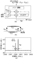
- C is a spectrum diagram showing an actual example of the blink frequency f LO signal generation of the present invention.
- FIG. 2 is a block diagram often used for explaining quadrature detection.
- quadrature detection of a modulated wave 20 having an input frequency f RF is performed using a reference carrier wave 30 having a frequency f RF .
- the input signal is split into two, one of which is mixed by the mixer 21 with the sine wave of the reference carrier 30 and the low frequency component is filtered and output as an in-phase (I) component.
- the other one of the two branches is mixed with the cosine wave of the reference carrier wave 30 by the mixer 21, and the low frequency component is filtered and output as a quadrature (Q) component.
- the amplitude and phase of the modulated wave input from the in-phase component and the quadrature component can be easily obtained.
- the mixer 25 that performs frequency conversion of the modulated wave 20 of the frequency f RF in FIG. 3A and the subsequent filter can be the same on the in-phase channel side and the quadrature channel side, FIG. As shown in (b), it is clear that there is no functional change even if the output of the mixer 29 and the subsequent filter is branched. By performing frequency conversion in this way, even when the frequency region applicable to the quadrature detector 100 is a relatively low region, it can be configured to be applicable to a higher frequency region than the quadrature detector 100 itself. It is clear.
- the reference carrier wave 30 having the frequency f RF is mixed with the output of the local oscillator 28 and frequency-converted to the frequency f IF .
- the frequency is converted to the frequency f IF by the mixer 27 and the subsequent filter, so that the frequency of the reference carrier wave of the quadrature detector 100 from the beginning.
- f IF a frequency conversion by the mixer 27 can be omitted.
- FIG. 4A and FIG. 4B are block diagrams showing configurations closer to the embodiment of the present invention than in the case of FIG. 4 (a) and 4 (b), the modulated wave 20 of the frequency f RF having the sideband SB1 is an input modulated wave, and the sideband SB2 corresponds to the reference carrier wave in FIGS. 3 (a) and 3 (b).
- This is a modulated wave 35 of frequency f RF having This modulated wave 35 corresponds to a reference carrier wave whose acquisition position is fixed.
- the difference between the frequency f RF of the modulated wave 20 and the frequency f RF of the modulated wave 35 is predominantly phase.
- the frequency shifter 34 only the frequency is shifted to a modulated wave 36 of the frequency f LO having the sideband SB2.
- the modulated wave 20 and the modulated wave 37 are mixed and filtered by the mixer 25 and the subsequent filter, and converted to the modulated wave 37 having the side band SB3 and having the frequency f IF . Further, the frequency conversion of the frequency f RF of the input modulated wave 20 from the analyte, instead of doing so the output of the local oscillator 28, frequency conversion to the frequency f LO inputs a predetermined signal frequency f RF from the specimen This is performed by the mixer 25 using the obtained signal. The frequency difference (
- the signal generator 33 generates a signal with a frequency f IF that is shifted from the frequency f P from the signal generator 32 by ⁇ f.
- the signal generator 3 Signal of the frequency f P from 2 applies as a reference carrier to the quadrature detector 100. Therefore, In the quadrature detector 100, the frequency of the input modulated wave is f IF , but the frequency f P of the reference carrier is shifted from f IF by ⁇ f.
- the reason why the frequency is intentionally shifted by the frequency ⁇ f is to obtain the phase obtained as a result of the quadrature detection as a linear function of time with ⁇ f as a coefficient.
- the frequency ⁇ f is input by the user of the electric field imaging apparatus or selected from a plurality of candidates.
- the phase of the modulated wave 20 having the frequency f RF is dynamically changed and becomes easy to see.
- the phase value obtained by the quadrature detection can be displayed directly or using a MOD function, or by taking the sine thereof, and the phase value can be displayed as a black-and-white shading pattern of wavelength intervals.
- the phase change in the input modulated wave 20 can be grasped as a change in the black and white shading pattern in the display.
- the MOD function is used or the sine of the phase value is taken, it can be expressed by the number of striped patterns such as contour lines.
- the block diagram of FIG. 4B is a configuration example when the quadrature detector 200 is configured by a digital circuit.
- the modulation wave 20 of the frequency f RF having the sideband SB1 is an input modulation wave having position dependency, and the frequency f having the sideband SB2 is obtained.
- the RF modulation wave 35 corresponds to a reference carrier wave whose acquisition position is fixed.
- the difference between the frequency f RF of the modulated wave 20 and the frequency f RF of the modulated wave 35 is predominantly phase.
- the frequency shifter 34 only the frequency is shifted to a modulated wave 36 of the frequency f LO having the sideband SB2.
- the modulated wave 20 and the modulated wave 37 are mixed and filtered by the mixer 25 and the subsequent filter, converted into a modulated wave 37 having a frequency f IF having a sideband SB3, and an input modulated wave of the quadrature detector 200.
- the frequency shifted by the frequency shifter 34 is the frequency f IF of the signal from the signal generator 33.
- This frequency f IF is a frequency shifted from the reference carrier frequency f P of the quadrature detector 200, which is a signal from the signal generator 32, by M (1 or ⁇ 1) times by the frequency ⁇ f.
- the digital circuit is processed in accordance with, for example, a well-known quadruple frequency sampling method.
- Frequency of quantization in A / D converter 32 is four times the frequency f P, the frequency f P is the frequency of the image frame obtained by calculating the imaging frame.
- the display on the computer 5 is performed at the display frame rate, the image frame data is converted into display frame data after signal processing as necessary. At that time, frame rate conversion may be performed.
- FIG. 5 shows a block diagram of the electric field imaging apparatus of the present invention.
- the birefringence of the electro-optic crystal plate (EO crystal, for example, ZnTe crystal) of the electric field sensor unit 9 is changed by the high-frequency electric field in the vicinity of the specimen (DUT) 10.
- the light incident on the electric field sensor unit 9 through the optical system 8 is modulated by the polarized light having a wavelength of 780 nm from the blinking light source 3.
- the surface of the electric field sensor unit 9 close to the specimen is subjected to a high reflectivity film (HR) treatment, and the polarized light irradiated to the surface is immediately after passing through the electro-optic crystal plate.
- HR high reflectivity film
- the polarization beam splitter 11 has a high transmittance for the polarized light from the blinking light source 3, but the polarized light tilted with respect to this polarized light is arranged so that the reflectance increases according to the tilt angle. Is. For this reason, the polarization component whose polarization plane is modulated by the electro-optic crystal plate is reflected by the polarization beam splitter 11 and enters the CMOS type imaging device 4.
- the image obtained by the imaging device 4 is subjected to image processing and arithmetic processing necessary for digital quadrature detection in the computer 5, and is subjected to statistical processing such as averaging and conversion to a display frame rate as necessary.
- the An optical image of the specimen 10 is captured by the CCD imaging device 7 via the dichroic mirror 12 under illumination by the LED 6 emitting 640 nm, and is displayed by the computer 5 in a manner superimposed on the image by the imaging device 4. .
- the high reflectance film (HR) has a characteristic of transmitting the light of the LED 6.
- the wavelength of polarized light emitted from the blinking light source can be sufficiently separated from the wavelength of illumination light from the LED 6 by a dichroic mirror, and the light from the LED 6 is imaged by the polarization beam splitter. It is desirable to have an arrangement and polarization characteristics that are less likely to be reflected by the user.
- the configuration of the block diagram of FIG. 5 is in accordance with the concept of FIG.
- the phase has position dependency.
- a frequency-shifted signal corresponding to the modulated wave 35 in FIG. 4 is input to the antenna 1. This is a radio wave received from the specimen 10, and the relative position between the antenna and the EO crystal plate is fixed, so that a reference phase to the input modulated wave of each pixel is formed.
- This frequency-shifted signal is shifted by the frequency f IF by the frequency shifter 2.
- This frequency f IF is a signal generated by shifting the frequency of a signal generated based on a signal generated from the internal clock of the CMOS imaging device 4, for example, a signal synchronized with the generation timing of the image frame by ⁇ f.
- the output of the frequency shifter 2 shifted by the frequency f IF is superimposed on the light beam from the blinking light source, mixed with the input modulated wave by the electric field sensor unit 9, and becomes a light beam on which the signal of the frequency f IF is superimposed.
- the image is picked up by the CMOS type image pickup device 4.
- processing by a quadruple frequency sampling method is performed, and an image frame is output at a frequency f P.
- the image pickup device 4 is a CMOS image pickup device.
- CMOS image pickup device it is a CCD type, when imaging at a high frame rate, a CMOS type imaging device is more suitable because noise characteristics are good.
- the blinking signal of the blinking light source 3 may be generated by combining the signal based on the clock for controlling the CMOS imaging device 7 and the signal obtained by picking up the signal from the specimen 10 with the antenna 1 with the frequency shifter 2.
- Examples of the frequency shifter 2 described above include an image removal mixer and a single sideband mixer.
- the signal from the antenna 1 is input to the frequency shifter 2 via the delay compensator 13.
- This delay compensator is for compensating for the time lag between the high-frequency electric field signal directly flying from the specimen 10 and the high-frequency signal via the antenna 1 on the electric field sensor 9.
- the delay compensator 13 is disposed on the electric signal path of the high-frequency signal from the antenna 1 to the computer 5.
- the signal for the blinking light source 3 can also be generated as shown in FIG.
- the signal of the frequency f RF from the antenna 1 is mixed with the signal of the frequency f LO1 , and once converted into an intermediate signal of the frequency f IF2 , and again the frequency
- a frequency f LO very close to the frequency f RF is realized. Specifically, this is performed by the following procedure.
- a high-frequency signal from the specimen (DUT) 10 is taken in via the antenna 1. This is used as a frequency-shifted signal and corresponds to the modulated wave 35 having the frequency f RF described above. This high-frequency signal is used to generate a signal having the frequency f LO by the frequency shifter 2 in FIG. It is also possible to use an independent EO crystal by capturing an electric field signal of a specific portion.
- a predetermined reference signal having a frequency f LO1 (for example, f LO1 is a sine wave of about 2 GHz with respect to 2.4 GHz f RF ) and a signal having a frequency f RF are mixed by a mixer.
- the first reference signal having the frequency f LO1 is a reference signal generated using a reference signal based on a clock for controlling the frame rate of the imaging device 7.
- the frequency of the first reference signal is sufficiently high so that the filter can sufficiently suppress signals having the frequency f RF and higher, and it is necessary to determine the frequency according to the performance of the filter.
- the second reference of the frequency f LO2 that is a signal having a predetermined frequency difference L IF from the first reference signal.
- the second reference signal having the frequency f LO2 is also a reference signal generated using a reference signal based on a clock for controlling the imaging device 7.
- the first reference signal and the second reference signal are generated using a reference signal based on a clock for controlling the imaging device 4, thereby obtaining an imaging frame rate in the imaging device 4.
- the values of f LO2 and f LO1 when a negative frequency is allowed for the frequency f IF are also effective values that can be actually applied.
- the frame rate assumed in the present invention is the imaging frame rate when the imaging device captures an image, the image frame rate when the data from the imaging device is processed and output as an image, and an image at the image frame rate for the display device This is the display frame rate that has been converted or processed into the image.
- the image frame rate will be described in more detail. It is a frame rate obtained as an image.
- the frame rate of the imaging device is set to f IS .
- f P f IS / 4
- f P f IS .
- the frequency ⁇ f is preferably a value set by the user of the electric field imaging apparatus of the present invention or a value selected from a plurality.
- the signal of the frequency f LO generated as described above is amplified in the power adjustment unit of FIG. 6A through the second-stage filter (not illustrated). And supplied to the blinking light source 3.
- the computer 5 that is an information processing means includes an image processing unit, an arithmetic processing unit, a control unit, a display unit, and the like, and shares their functions.
- image processing unit an image signal from the CMOS image pickup device 4 is input, and quadrature detection is performed for each pixel. This quadrature detection can be digitally processed by a quadruple frequency sampling method. Further, the calculation processing unit detects the amplitude component and the phase component separately.
- the control unit and the display unit store the information for each pixel of the amplitude component and the phase component as an image in the computer 5, transmit it, or display it on the display unit.
- the second reference of the frequency f LO2 that is a signal having a predetermined frequency difference L IF from the first reference signal.
- the second reference signal having the frequency f LO2 is also a reference signal generated using a reference signal based on a clock for controlling the imaging device 7.
- the values of f LO2 and f LO1 when a negative frequency is allowed for the frequency L IF are also effective values that can be actually applied.
- FIG. 7 shows 2.4 GHz emitted from a chip antenna mounted on-board Bluetooth “Bluetooth®” module. It is the result applied to radio waves.
- This commercially available module has a built-in crystal resonator type free-running signal source, but there is no synchronization signal input / output or RF signal extraction terminal.
- FIG. 7A is a diagram showing that a high-frequency signal from a specimen is inputted, frequency-converted as it is, and applied to a blinking light source
- FIG. 7B shows a side view of the module
- FIG. 7A is a diagram showing that a high-frequency signal from a specimen is inputted, frequency-converted as it is, and applied to a blinking light source
- FIG. 7B shows a side view of the module
- An overhead view of the specimen along the z-axis is shown. It is an optical image imaged through an EO crystal plate.
- D shows the actual measurement of the electric field strength distribution in the vicinity of the chip antenna reflecting the characteristics of the chip antenna, the influence on the radio wave radiation of the on-board module substrate and the USB interface substrate. It is superimposed on the optical image.
- E is a wavefront progress strobe diagram sequence displayed superimposed on an optical image, 8 shots per ⁇ / 6, and
- (f) is an electric field phasor progress strobe diagram sequence, 8 shots per ⁇ / 6.
- (g) is a diagram showing a wave vector distribution by an imaged complex two-dimensional Fourier transform.
- phase progress in the high-frequency device is captured as an image according to the present invention.
- time spent for module and product operation and failure analysis and diagnosis, EMC countermeasures, etc. will be greatly shortened, and competitiveness in terms of cost and performance will be enhanced.
Landscapes
- Physics & Mathematics (AREA)
- General Physics & Mathematics (AREA)
- Nonlinear Science (AREA)
- Optics & Photonics (AREA)
- Electromagnetism (AREA)
- Engineering & Computer Science (AREA)
- Multimedia (AREA)
- Signal Processing (AREA)
- Investigating Or Analysing Materials By Optical Means (AREA)
- Studio Devices (AREA)
Abstract
実際の製品を引出し線なしの製品の状態で検体に用い、その近傍の電磁界の強度の分布と位相の遅れ進みの分布を動態として可視化できる電界イメージング装置を実現する。 検体が発する高周波信号を入力するアンテナと、周波数fRFの高周波電界のセンサーであるEO結晶板と、EO結晶板に偏光を照射する明滅光源と、EO結晶板を介して得たその偏光の位相変化を検出する検光子に導く光学系と、検光子からの光束の面内分布を電気信号に変換する撮像装置と、その出力信号を処理し表示する情報処理装置とを備える。検体とは独立な所定の周波数fIFでアンテナからのfRFの高周波信号を周波数変換し、fRFに近い周波数帯の信号を生成して明滅光源用信号とし、EO結晶板に明滅光を照射して高周波電界信号の周波数下方変換信号を撮像装置で読み取り、その出力を直交検波して、高周波電界信号の振幅や位相の分布を画像化する。
Description
この発明は、高周波振動電界の2次元分布とその時間的および空間的変化を実時間で可視化することができる電界イメージング装置に関する。
上記の高周波電界の2次元分布の可視化を実時間で行うものとしては、国立研究開発法人情報通信研究機構から報告された電界カメラ(非特許文献1)が知られており、これは、特許文献1に記載の電磁界高速撮像装置やその後の改良等に基づくものである。この電界カメラは、電気光学効果を介して光の超並列性と超高速性が重畳的に活用され、100GHzまでのマイクロ波帯の電界分布が実時間で撮像かつ表示される装置である。
「実時間」という限定をつけなければ、既に様々な形態の電界分布映像化技術が提案され、また実現されている。これまで、様々な回路や機器の周囲の電界が撮像され、それらの回路や機器の解析に用いられてきたが、従来は、空間走査に長時間が必要であった。このような制約の下でも、電界を可視化する努力は続けられてきており、実時間映像化への期待は従来から大きなものであった。
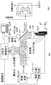
上記電界カメラのブロック図を図1(a)に、そのドライバー部を図1(b)に示す。特許文献1に従えば、このドライバー部は、明滅光源のfLO発振部と検体用のfRF発振部から成っている。この電界カメラでは、明滅光源から周波数fLOで振幅変調された偏光を照明光として電気光学(EO)結晶板(特許文献1の標記でプローブ)に照射すると、検体(DUT)から放射される周波数fRFの電波の電界によりEO結晶板の複屈折特性が変化することで、上記照明光の偏波面には各位置の複屈折の変化を反映した変化が与えられる。このように偏波面の変化した偏光を検光子を含む光学系で選択し、この2次元分布をイメージセンサで撮像する。これによって、上記照明光の変調周波数(fLO)と上記検体から放射される電磁界の周波数(fRF)との差周波成分(特許文献1の標記でΔf(=|fLO-fRF|))を含む検出光について上記イメージセンサの画素毎の信号が並列に得られる。この信号は、画素ごとに順次出力され、画像処理装置で演算処理の後、画像表示装置に表示される。
この電界カメラを用いた電界映像化技術では、撮像対象の高周波電気信号と撮像システム内部の高速CMOSイメージセンサ(IS)のサンプリングとは互いに同期するものであった。これは、イメージセンサの各画素で行われる一括の周波数変換の結果の表示における不安定性や消滅を避けるためである。
この同期を実現するために、従来は、図1(b)に示すように、上記周波数fLO用と上記周波数fRF用との各信号源には外部信号源からの参照信号に同期可能なものを用いてきた。このため、上記信号源については、ISがマスターであり、DUT動作がスレーブであった。すなわち、従来は、同期モードかつマスターモードのシステムによる電界撮像であった。
つまり、図l(b)に示すように周波数fLO用の信号源(LO信号源)もIS参照信号に同期させる。これは、RF信号との上記差周波成分ΔfがISサンプリングのタイミングと同期する必要があるためである。さらに、差周波成分Δfの帯域は動画フレームレート(典型的には10Hz)以下に制約されるが、これを実現するためには、RF信号の瞬時周波数が変調やデータ重畳などで変動した場合に、周波数fLO用の信号とRF信号との周波数差Δfを維持するように周波数fLO用の信号がRF信号に追随する必要があり、D
UTとLO信号源の双方に制約を与えていた。
UTとLO信号源の双方に制約を与えていた。
この様に、従来の電界カメラシステムの観察対象となり得る検体は大きく限定されていた。例えば、外部信号源(主としてシンセサイザ)に同期可能な検体か、ISクロックに
対して同期できる機能を備えた検体か、に限られた。一般に、市販の製品あるいはその製品内部で使用されている高周波モジュールでは、同期機能を有する回路の追加や信号入出力用の配線を増設する等の改造することが求められ、改造なしに上記の検体となり得るものは稀であった。
対して同期できる機能を備えた検体か、に限られた。一般に、市販の製品あるいはその製品内部で使用されている高周波モジュールでは、同期機能を有する回路の追加や信号入出力用の配線を増設する等の改造することが求められ、改造なしに上記の検体となり得るものは稀であった。
また、ここで用いる信号は上記の様にISからの参照信号に同期させることになるが、この様に同期させるため、また、上述の追随性の必要のために、上記周波数fLO用と上記周波数fRF用との各信号源には周波数シンセサイザが用いられてきた。しかしこの場合、それぞれの帯域幅は1Hz以下であり、RF信号自体は極めて狭帯域だった。実際の自走
型信号源を有するモジュールやそれを用いた機器では、一般に、変動が大きくその帯域幅も大きい。この変動はそれぞれの高周波機器毎に異なっているが、検体に合わせた帯域幅を実現できることが望ましい。
型信号源を有するモジュールやそれを用いた機器では、一般に、変動が大きくその帯域幅も大きい。この変動はそれぞれの高周波機器毎に異なっているが、検体に合わせた帯域幅を実現できることが望ましい。
M. Tsuchiya and T. Shiozawa, "Photonics makes microwaves visible," Research Highlights, IEEE Photonics Society Newsletter, Vol, 26, Number6, December 2012, pp,9-17.
実際の製品あるいは開発中の試作品やモジュールで、位相同期機能を有する回路やブロックを追加したり、引き出し線を設けたりする等の加工をすることなく、製品あるいは開発中の試作品やモジュールのままの状態のものを検体として用いて、その近傍の電磁界の強度や位相の遅れ進みの分布およびその動態を可視化する。
本発明では、振動電磁界における振動電界を、EO結晶における電気光学効果を用いて観察する。その電気光学効果は、上記EO結晶を進む偏光の位相状態が変化する現象であり、本発明では1往復させて、その位相変化を検出し電界強度を観察するものである。このような位相変化を検出するため、上記のEO結晶に偏光を照射し、その透過光から位相変化した偏光を検光子で選択し、光電変換して検出する。
このため本発明の電界イメージング装置は、
周波数fRFを中心とする周波数帯にある高周波信号および高周波電界信号を発する検体付近の電界分布とその時間的変動を観察する電界カメラであって、
上記検体が発する高周波信号を入力する高周波信号入力手段と、
上記高周波電界のセンサーであるEO結晶板と、
上記EO結晶板に明滅する偏光を照射する明滅光源と、
上記偏光を、上記EO結晶板を介して、その偏光の位相変化を検出する検光子に導く光学系と、
上記偏光による上記検光子からの光束の面内分布を電気信号に変換する撮像手段と、
上記撮像手段からの出力信号を検波処理し画像フレームを周波数fPで出力する信号処
理手段と、上記信号処理手段の出力の演算処理、表示、伝送または保存する情報処理手段と、
上記検体とは独立な所定の周波数の信号を用いて、上記高周波信号入力手段から入力された高周波信号を周波数fLOを中心周波数とする信号に変換して出力する明滅信号生成手段と、を備え、
上記明滅光源は上記明滅信号生成手段の出力に従って上記周波数fLOで明滅するものであり、
上記周波数fRFと上記周波数fLOとの差に相当する周波数fIFは、上記周波数fPの1
倍あるいは-1倍からゼロ以外の周波数δf分ずれた周波数であり、
上記信号処理手段の出力を上記画像フレームの画素ごとに、上記周波数fPの信号を参
照搬送波として直交検波を行うことで、上記高周波電界信号の振幅または位相の位置依存性とその変化を表示、伝送または保存するものである。
周波数fRFを中心とする周波数帯にある高周波信号および高周波電界信号を発する検体付近の電界分布とその時間的変動を観察する電界カメラであって、
上記検体が発する高周波信号を入力する高周波信号入力手段と、
上記高周波電界のセンサーであるEO結晶板と、
上記EO結晶板に明滅する偏光を照射する明滅光源と、
上記偏光を、上記EO結晶板を介して、その偏光の位相変化を検出する検光子に導く光学系と、
上記偏光による上記検光子からの光束の面内分布を電気信号に変換する撮像手段と、
上記撮像手段からの出力信号を検波処理し画像フレームを周波数fPで出力する信号処
理手段と、上記信号処理手段の出力の演算処理、表示、伝送または保存する情報処理手段と、
上記検体とは独立な所定の周波数の信号を用いて、上記高周波信号入力手段から入力された高周波信号を周波数fLOを中心周波数とする信号に変換して出力する明滅信号生成手段と、を備え、
上記明滅光源は上記明滅信号生成手段の出力に従って上記周波数fLOで明滅するものであり、
上記周波数fRFと上記周波数fLOとの差に相当する周波数fIFは、上記周波数fPの1
倍あるいは-1倍からゼロ以外の周波数δf分ずれた周波数であり、
上記信号処理手段の出力を上記画像フレームの画素ごとに、上記周波数fPの信号を参
照搬送波として直交検波を行うことで、上記高周波電界信号の振幅または位相の位置依存性とその変化を表示、伝送または保存するものである。
また、上記高周波信号入力手段から上記信号処理手段に至る上記高周波信号の電気信号経路上に、上記高周波信号の遅延補償を行う遅延補償手段を備えるものである。
また、上記情報処理手段は、画像信号から分離された位相信号にゼロでない所定の値を乗じた値を用いて上記表示装置用の表示画像用の画像信号を生成するものである。これによって、例えば位相の位置依存とその変化を強調することができる。
上記明滅信号生成手段は、
(1)所定の周波数fLO1の信号と上記高周波信号入力手段から入力した周波数fRFの信
号とを混合して差周波数側(fRF-fLO1)の周波数(fIF2=fRF-fLO1)の信号を生
成し、
(2)上記周波数fLO1の信号とは所定の周波数差(正負を許容するfIF)である周波数
fLO2(=fLO1-fIF)の信号と上記(1)で生成された信号とを混合して和周波数側(fIF2+fLO2)の周波数(fLO=fRF-fIF)の信号を生成することによって、周波数fRFに極近い周波数(fLO)の信号を生成するものである。
(1)所定の周波数fLO1の信号と上記高周波信号入力手段から入力した周波数fRFの信
号とを混合して差周波数側(fRF-fLO1)の周波数(fIF2=fRF-fLO1)の信号を生
成し、
(2)上記周波数fLO1の信号とは所定の周波数差(正負を許容するfIF)である周波数
fLO2(=fLO1-fIF)の信号と上記(1)で生成された信号とを混合して和周波数側(fIF2+fLO2)の周波数(fLO=fRF-fIF)の信号を生成することによって、周波数fRFに極近い周波数(fLO)の信号を生成するものである。
また、上記明滅信号生成手段は、
(1)所定の周波数fLO1の信号と上記高周波信号入力手段から入力した周波数fRFの信
号とを混合して和周波数側(fRF+fLO1)の周波数(fIF2=fRF+fLO1)の信号を生
成し、
(2)上記周波数fLO1の信号とは所定の周波数差(正負を許容するfIF)である周波数
fLO2(=fLO1-fIF)の信号と上記(1)で生成された信号とを混合して差周波数側(fIF2-fLO2)の周波数(fLO=fRF+fIF)の信号を生成することによって、周波数fRFに極近い周波数(fLO)の信号を生成するものであってもよい。
(1)所定の周波数fLO1の信号と上記高周波信号入力手段から入力した周波数fRFの信
号とを混合して和周波数側(fRF+fLO1)の周波数(fIF2=fRF+fLO1)の信号を生
成し、
(2)上記周波数fLO1の信号とは所定の周波数差(正負を許容するfIF)である周波数
fLO2(=fLO1-fIF)の信号と上記(1)で生成された信号とを混合して差周波数側(fIF2-fLO2)の周波数(fLO=fRF+fIF)の信号を生成することによって、周波数fRFに極近い周波数(fLO)の信号を生成するものであってもよい。
また、上記明滅信号生成手段に用いられる上記検体とは独立な所定の周波数の信号は、単一または複数であって、各々上記撮像手段の撮像フレームレートを制御するクロックに基づく参照信号を用いて生成した信号であることが望ましい。
また、振動電磁界における振動磁界を、磁気光学(MO)結晶における磁気光学効果を用いて観察することも可能である。その磁気光学効果は、上記MO結晶を透過または反射する偏光の偏波面が変調される現象であり、その偏波面の変調を検出して磁界強度を測定するものである。このような偏波面の変調は、上記のMO結晶に偏光を照射し、その透過光や反射光から偏波面の変調を受けた偏光を検光子で選択し、光電変換して検出する。
高周波信号装置に基準となる高周波信号を導入するための配線やその導入のための同期
回路ブロック等を追加する等の加工をすることなく、上記の高周波信号装置の電磁界を可視化することができ、しかも、位相変化の動向を動画として表示できるようになる。これにより、高周波回路の動作について目視の上で検査や故障診断が可能になる。
回路ブロック等を追加する等の加工をすることなく、上記の高周波信号装置の電磁界を可視化することができ、しかも、位相変化の動向を動画として表示できるようになる。これにより、高周波回路の動作について目視の上で検査や故障診断が可能になる。
図2と図3と図4に本発明の原理を示す。
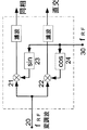
図2は、直交検波の説明によく使われるブロック図である。このブロック図においては、入力の周波数fRFの変調波20を周波数fRFの参照搬送波30で直交検波を行うものである。入力信号は2分岐され、その一方は混合器21で参照搬送波30の正弦波と混合され、低周波数成分が濾波され、同相(I)成分として出力される。また、2分岐された他の一方は、混合器21で参照搬送波30の余弦波と混合され、低周波数成分が濾波され、直交(Q)成分として出力される。これら同相成分と直交成分とから入力された変調波の振幅と位相を容易に得ることができる。
図2は、直交検波の説明によく使われるブロック図である。このブロック図においては、入力の周波数fRFの変調波20を周波数fRFの参照搬送波30で直交検波を行うものである。入力信号は2分岐され、その一方は混合器21で参照搬送波30の正弦波と混合され、低周波数成分が濾波され、同相(I)成分として出力される。また、2分岐された他の一方は、混合器21で参照搬送波30の余弦波と混合され、低周波数成分が濾波され、直交(Q)成分として出力される。これら同相成分と直交成分とから入力された変調波の振幅と位相を容易に得ることができる。
ここで、上記図2の構成を、図3(a)に示す様に、周波数fRFの変調波20と周波数fRFの参照搬送波30を、共通の局部発振器28からの出力を分岐した波で周波数変換を行うように変更しても、周波数変換による効果が混合器21あるいは22で相殺されることから、直交検波機能に変わりが無く周波数fRFの変調波の振幅と位相を容易に得ることができることは明らかである。
また、図3(a)の周波数fRFの変調波20の周波数変換を行う混合器25とそれに続
く濾波器は、同相チャネル側と直交チャネル側とで同じものを用いることができることから、図3(b)に示す様に、混合器29とそれに続く濾波器の出力を分岐して用いることでも機能的に変更がないことは明らかである。
この様に周波数変換を行うことにより、直交検波器100に適用できる周波数領域が比較的低い領域である場合でも、直交検波器100自体より高い周波数領域に適用できるように構成することが可能であることは明らかである。
く濾波器は、同相チャネル側と直交チャネル側とで同じものを用いることができることから、図3(b)に示す様に、混合器29とそれに続く濾波器の出力を分岐して用いることでも機能的に変更がないことは明らかである。
この様に周波数変換を行うことにより、直交検波器100に適用できる周波数領域が比較的低い領域である場合でも、直交検波器100自体より高い周波数領域に適用できるように構成することが可能であることは明らかである。
また、図3(a)のブロック図では、周波数fRFの参照搬送波30は、局部発振器28の出力と混合され周波数fIFに周波数変換されるが、図3(b)に示す様に、局部発振器28の出力周波数fLOを、fLO=fRF-fIF、とすると、混合器27とそれに続く濾波器により周波数fIFに変換されるので、当初から直交検波器100の参照搬送波の周波数をfIFとすることで混合器27による周波数変換を省くことができる。
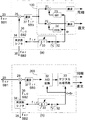
図4(a)および(b)の、図3の場合に比べて、本発明の実施形態により近い構成のブロック図を示す。図4(a)、(b)では、側帯波SB1を持った周波数fRFの変調波20が入力変調波であり、図3(a)(b)における参照搬送波に相当するのが側帯波SB2を持った周波数fRFの変調波35である。この変調波35が取得位置が固定された参照搬送波に相当する。周波数fRFの変調波20と周波数fRFの変調波35との違いは主に位相である。周波数シフター34では、周波数のみがシフトされ側帯波SB2を持った周波数fLOの変調波36になる。上記変調波20と変調波37が混合器25とそれに続く濾波器で混合および濾波され側帯波SB3を持った周波数fIFの変調波37に変換される。また、検体からの周波数fRFの入力変調波20の周波数変換を、局部発振器28の出力で行うのではなく、その検体からの周波数fRFの所定の信号を入力し上記周波数fLOに周波数変換した信号を用いて混合器25で行う。これらの信号の周波数差(|fRF-fLO|)は、信号生成器33からの周波数fIFの信号で補う。この信号生成器33は、信号生成器32からの周波数fPからδf分ずれた周波数fIFの信号を生成する。また、信号生成器3
2からの周波数fPの信号は、直交検波器100に参照搬送波として印加する。従って、
直交検波器100では、入力変調波の周波数はfIFであるが、その参照搬送波の周波数fPは、fIFからδf分ずれていることになる。
2からの周波数fPの信号は、直交検波器100に参照搬送波として印加する。従って、
直交検波器100では、入力変調波の周波数はfIFであるが、その参照搬送波の周波数fPは、fIFからδf分ずれていることになる。
この様に、上記周波数を意図的に周波数δf分ずらす理由は、直交検波の結果として得られる位相を、δfを係数とする時間の一次関数として得るためである。
この周波数δfは、この電界イメージング装置の使用者によって入力されるか、複数の候補から選択されるものである。
この周波数δfは、この電界イメージング装置の使用者によって入力されるか、複数の候補から選択されるものである。
このようにδf分ずれていることによって、周波数fRFの変調波20における位相が動的に変化して見やすくなる。例えば、直交検波によって得られる位相の値を直接、あるいはMOD関数を使用して、あるいはその正弦をとることで位相の値を波長間隔の白黒濃淡パターンにして表示することができる。この場合、入力される変調波20における位相の変化は、表示における白黒濃淡パターンの変化として捉えることができる。MOD関数を使用するか位相の値の正弦をとる等の場合には、等高線のように、縞模様の数でも表すことができる。
図4(b)のブロック図は、直交検波器200をデジタル回路で構成する場合の構成例である。この構成例は、図4(a)の場合と同様に、側帯波SB1を持った周波数fRFの変調波20が位置依存性をもった入力変調波であり、側帯波SB2を持った周波数fRFの変調波35が取得位置が固定された参照搬送波に相当する。周波数fRFの変調波20と周波数fRFの変調波35との違いは主に位相である。周波数シフター34では、周波数のみがシフトされ側帯波SB2を持った周波数fLOの変調波36になる。上記変調波20と変調波37が混合器25とそれに続く濾波器で混合および濾波され側帯波SB3を持った周
波数fIFの変調波37に変換され、直交検波器200の入力変調波となる。周波数シフター34でシフトされる周波数は、信号生成器33からの信号の周波数fIF分である。この周波数fIFは、信号生成器32からの信号である直交検波器200の参照搬送波の周波数fPのM(1あるいは-1)倍から周波数δf分ずらした周波数である。
波数fIFの変調波37に変換され、直交検波器200の入力変調波となる。周波数シフター34でシフトされる周波数は、信号生成器33からの信号の周波数fIF分である。この周波数fIFは、信号生成器32からの信号である直交検波器200の参照搬送波の周波数fPのM(1あるいは-1)倍から周波数δf分ずらした周波数である。
デジタル回路の処理は、例えば既によく知られた4倍周波数サンプリング法に従って行う。A/D変換器32での量子化の周波数は、上記周波数fPの4倍であり、周波数fPは
撮像フレームを演算して得られる画像フレームの周波数である。因みに、コンピュータ5での表示は表示フレームレートで行われるので、必要に応じて、画像フレームデータは、信号処理の後、表示フレームデータに変換される。その際、フレームレートの変換が行われる場合もある。
撮像フレームを演算して得られる画像フレームの周波数である。因みに、コンピュータ5での表示は表示フレームレートで行われるので、必要に応じて、画像フレームデータは、信号処理の後、表示フレームデータに変換される。その際、フレームレートの変換が行われる場合もある。
以下に、この発明の実施の形態を図面に基づいて詳細に説明する。以下の説明においては、同じ機能あるいは類似の機能をもった装置に、特別な理由がない場合には、同じ符号を用いるものとする。
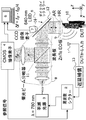
本発明の電界イメージング装置のブロック図を図5に示す。図5の構成では、検体(DUT)10の近傍の高周波電界によって、電界センサー部9の電気光学結晶板(EO結晶、例えばZnTe結晶)の複屈折率が変化する。この複屈折率の変化で、明滅光源3からの波長780nmの偏光で光学系8を通じてこの電界センサー部9に入射した光を変調する。この電界センサー部9の検体に近い面には、高反射率膜(HR)処理が施されており、これに照射された偏光は、上記電気光学結晶板を透過した直後にこの高反射率膜で反射され、再び上記電気光学結晶板を透過して偏光変調を受ける。その後ダイクロイックミラー12で反射され、偏光ビーム分岐器11に入射する。この偏光ビーム分岐器11は、明滅光源3からの偏光には高い透過率を示すが、この偏光に対して傾いた偏光については、その傾き角度に応じて反射率が上昇する様に配置されたものである。このため上記電気光学結晶板で偏波面の変調された偏光成分は、偏光ビーム分岐器11で反射され、CMOS型撮像装置4に入射する。この撮像装置4による画像は、コンピュータ5で、デジタル直交検波に必要な画像処理や演算処理が施され、また必要に応じて平均化等の統計処理や表示フレームレートへの変換がなされ、表示される。また、検体10の光学画像は、640nm発光のLED6による照明下で、ダイクロイックミラー12を介して、CCD型撮像装置7により撮像され、コンピュータ5で、撮像装置4による画像と重畳されて表示される。上記高反射率膜(HR)は、LED6の光に対して透過する特性を有する。明滅光源の出射する偏光の波長は、LED6からの照明光の波長とは、ダイクロイックミラーで十分に分離できるものであることが望ましく、また、LED6からの光は、偏光ビーム分岐器で撮像装置4の方に反射されにくい配置や偏光特性を持っていることが望ましい。
図5のブロック図の構成は、図4(b)の概念に沿ったものである。入力変調波が電界センサー部9に入力されることによりその位相は位置依存性をもつ。また、図4の変調波35に相当する被周波数シフト信号は、アンテナ1に入力される。これは検体10から発せられる電波を受信したもので、アンテナとEO結晶板との相対位置は固定されるため各画素の入力変調波への基準位相を形成する。この被周波数シフト信号は、周波数シフター2で、周波数fIF分シフトされる。この周波数fIFは、CMOS型撮像装置4の内部クロックから生成された信号に基づいて生成された信号、例えば画像フレームの生成タイミングに同期した信号の周波数をδf分ずらした信号である。この周波数fIF分シフトされた周波数シフター2の出力は、明滅光源からの光束に重畳されて、電界センサー部9で上記入力変調波と混合されて上記周波数fIFの信号が重畳された光束となり、CMOS型撮像装置4で撮像される。このCMOS型撮像装置4では、4倍周波数サンプリング法による処理が行われて、画像フレームが周波数fPで出力される。
この撮像装置4には、種々のものを使用することができるが、この例ではCMOS型撮像装置である。CCD型のものを使用することも可能であるが、高フレームレートで撮像する場合は、ノイズ特性が良好なこともありCMOS型撮像装置の方が適している。
明滅光源3の明滅信号は、CMOS撮像装置7を制御するクロックに基づく信号と、検体10からの信号をアンテナ1で拾った信号とを周波数シフター2で合成して生成してもよい。上記のような周波数シフター2としては、イメージ除去ミキサーや単側帯波ミキサーなどがある。
ここで、アンテナ1からの信号は遅延補償器13を介して上記周波数シフター2に入力される。この遅延補償器は、上記電界センサー部9上で、検体10から直接飛来する高周波電界信号とアンテナ1を介した高周波信号との時間ずれを補うためのものである。上記アンテナ1からコンピュータ5至るまでの上記高周波信号の電気信号の経路上に、この遅延補償器13を配置する。
ここで、アンテナ1からの信号は遅延補償器13を介して上記周波数シフター2に入力される。この遅延補償器は、上記電界センサー部9上で、検体10から直接飛来する高周波電界信号とアンテナ1を介した高周波信号との時間ずれを補うためのものである。上記アンテナ1からコンピュータ5至るまでの上記高周波信号の電気信号の経路上に、この遅延補償器13を配置する。
また、明滅光源3用の信号は図6に示すように生成することもできる。この信号生成では、図6(b)に示すようにアンテナ1からの周波数fRFの信号を、周波数fLO1の信号
と混合して、一旦、周波数fIF2の中間信号に変換し、再度、周波数fLO2の信号で変換して、周波数fRFに極近い周波数fLOを実現する、というものである。これを、具体的には以下の手順で行う。
と混合して、一旦、周波数fIF2の中間信号に変換し、再度、周波数fLO2の信号で変換して、周波数fRFに極近い周波数fLOを実現する、というものである。これを、具体的には以下の手順で行う。
以下の手順は、2段階の周波数変換を行なって、元の周波数に極近い周波数の信号を生成するものである。
1-1:まず、アンテナ1を介して検体(DUT)10からの高周波信号を取り込む。これは、被周波数シフト信号として用い、上記の周波数fRFの変調波35に相当するが、この高周波信号は、図5の周波数シフター2で周波数fLOの信号を生成するために使われる。また、独立したEO結晶を設けて特定部分の電界信号を取り込んでこれを用いることも可能である。また、電界センサー部9の特定位置の連続読み出しを行って、上記と同様に周波数fLOの信号を生成するための被周波数シフト信号として用いる上記の周波数fRFの変調波35とすることも可能である。図5では、この取り込みをアンテナ1を介して行っているが、検体10に引き出し線がある場合は、それを用いて上記の取り込みを行うことも可能である。しかし、検体に非接触の状態で上記参照搬送波として用いる上記の周波数fRFの変調波35の取り込みを行うことが望ましい。
1-1:まず、アンテナ1を介して検体(DUT)10からの高周波信号を取り込む。これは、被周波数シフト信号として用い、上記の周波数fRFの変調波35に相当するが、この高周波信号は、図5の周波数シフター2で周波数fLOの信号を生成するために使われる。また、独立したEO結晶を設けて特定部分の電界信号を取り込んでこれを用いることも可能である。また、電界センサー部9の特定位置の連続読み出しを行って、上記と同様に周波数fLOの信号を生成するための被周波数シフト信号として用いる上記の周波数fRFの変調波35とすることも可能である。図5では、この取り込みをアンテナ1を介して行っているが、検体10に引き出し線がある場合は、それを用いて上記の取り込みを行うことも可能である。しかし、検体に非接触の状態で上記参照搬送波として用いる上記の周波数fRFの変調波35の取り込みを行うことが望ましい。
1-2:次に、周波数fLO1の所定の基準信号(例えば2.4GHzのfRFに対してfLO1は約2GHzの正弦波)と周波数fRFの信号とを混合器で混合して差周波側の周波数(fIF2=fRF-fLO1)の信号を濾波器(IF2BPF)で選択する。この周波数fLO1の第
1基準信号は、撮像装置7のフレームレートを制御するクロックに基づく参照信号を用いて生成した基準信号である。上記第1基準信号の周波数は、上記濾波器が上記周波数fRFおよびそれ以上の信号を充分抑圧できる程度に充分に高い周波数であり、濾波器の性能によって決定する必要がある。
1基準信号は、撮像装置7のフレームレートを制御するクロックに基づく参照信号を用いて生成した基準信号である。上記第1基準信号の周波数は、上記濾波器が上記周波数fRFおよびそれ以上の信号を充分抑圧できる程度に充分に高い周波数であり、濾波器の性能によって決定する必要がある。
1-3:次に、上記第1基準信号と所定の周波数差LIFの信号である周波数fLO2の第2
基準信号とを混合して和周波側の周波数(fLO=fIF2+fLO2)の信号を濾波器(図に記載していない)で選択する。ただし、周波数fLO2は、fLO2=fLO1-fIF、または、fLO2=fLO1+fIFとする。この周波数fLO2の第2基準信号も、撮像装置7を制御するクロックに基づく参照信号を用いて生成した基準信号である。
このように周波数fLOの信号を生成する場合、第1基準信号と第2基準信号とを撮像装置4を制御するクロックに基づく参照信号を用いて生成することによって撮像装置4にお
ける撮像フレームレートで混合を行うことは、直交検波の安定化に寄与する。つまり、CMOS型撮像装置4に入射する光束は周波数fLO(=fRF-fIF)で周波数変換されて周波数fIFとなった光束であり、周波数fRFに不安定部分が含まれている場合でも、上記撮像装置4内では、周波数fIF(=fP+δf)の周波数fP信号は上記クロックから生成されるものであるので、上記不安定部分は相殺され、安定に直交検波を行うことができる。
上記の2段階の周波数変換において、周波数fIFに負の周波数を許容した場合のfLO2やfLO1の値も実際に適用できる有効な値である。
基準信号とを混合して和周波側の周波数(fLO=fIF2+fLO2)の信号を濾波器(図に記載していない)で選択する。ただし、周波数fLO2は、fLO2=fLO1-fIF、または、fLO2=fLO1+fIFとする。この周波数fLO2の第2基準信号も、撮像装置7を制御するクロックに基づく参照信号を用いて生成した基準信号である。
このように周波数fLOの信号を生成する場合、第1基準信号と第2基準信号とを撮像装置4を制御するクロックに基づく参照信号を用いて生成することによって撮像装置4にお
ける撮像フレームレートで混合を行うことは、直交検波の安定化に寄与する。つまり、CMOS型撮像装置4に入射する光束は周波数fLO(=fRF-fIF)で周波数変換されて周波数fIFとなった光束であり、周波数fRFに不安定部分が含まれている場合でも、上記撮像装置4内では、周波数fIF(=fP+δf)の周波数fP信号は上記クロックから生成されるものであるので、上記不安定部分は相殺され、安定に直交検波を行うことができる。
上記の2段階の周波数変換において、周波数fIFに負の周波数を許容した場合のfLO2やfLO1の値も実際に適用できる有効な値である。
本発明で想定するフレームレートは、撮像装置が撮像する際の撮像フレームレート、その撮像装置からのデータを処理して画像として出力する際の画像フレームレート、その画像フレームレートの画像を表示装置用の画像に変換や加工した表示フレームレートである。その画像フレームレートについてより詳しく説明すると、それは画像として得られるフレームレートであって、例えば図4(b)の場合の様に4倍周波数サンプリングを行う場合、撮像装置のフレームレートをfISとするとき、fP=fIS/4であり、図4(a)に
示す様に、アナログ回路を用いる場合には、fP=fISである。
示す様に、アナログ回路を用いる場合には、fP=fISである。
また、fIFは、上記δfに上記撮像装置によって得られる画像フレームレートfPを、
加えたあるいは引いた値である。つまり、上記の様に、Mを1あるいは-1として、fIF=M×fP+δfである。周波数δfついては、本発明の電界イメージング装置の使用者
が設定した値または複数から選択した値とすることが望ましい。
ここで、M=0に設定する場合は、CMOS型撮像装置4に入射する光束をCMOS型撮像装置4の代わりに配列したフォトダイオード等で光電変換することで、上記入力変調波の位相情報を得ることができる。
加えたあるいは引いた値である。つまり、上記の様に、Mを1あるいは-1として、fIF=M×fP+δfである。周波数δfついては、本発明の電界イメージング装置の使用者
が設定した値または複数から選択した値とすることが望ましい。
ここで、M=0に設定する場合は、CMOS型撮像装置4に入射する光束をCMOS型撮像装置4の代わりに配列したフォトダイオード等で光電変換することで、上記入力変調波の位相情報を得ることができる。
1-4:次に、上記の様に生成された周波数fLOの信号を第二段の濾波器(図には描かれていない)を介して、図6(a)のパワー調整部において増幅し、明滅光源3に供給する。
なお、一般に、濾波器は、回路の周波数特性を用いてその代用とすることができる場合があることはよく知られており、この事情は、本発明に於いても同様である。
情報処理手段であるコンピュータ5には、画像処理部、演算処理部、制御部、表示部などがあり、それぞれの機能を分担している。その画像処理部では、CMOS型撮像装置4からの画像信号を入力し、各ピクセルについて、直交検波を行う。この直交検波を4倍周波数サンプリング法でデジタル処理することも可能である。また、その演算処理部で振幅成分と位相成分とに分けて検出する。また、その制御部と表示部とで、上記の振幅成分と位相成分の各ピクセルごとの情報を画像として、コンピュータ5に保存するか、伝送するか、またはその表示部に表示する。
上記の手順(1-2)と(1-3)の代わりに、次の様にすることもできる。
2-2:周波数fLO1の所定の基準信号(例えば2.4GHzのfRFに対してfLO1は約2GHzの正弦波)と周波数fRFの信号とを混合器で混合して和周波側の周波数(fIF2=
fRF+fLO1)の信号を濾波器(IF2BPF)で選択する。この場合の濾波器は上記周
波数fRFおよびそれ以下の信号を充分抑圧できるものである。
2-3:次に、上記第1基準信号と所定の周波数差LIFの信号である周波数fLO2の第2
基準信号とを混合して差周波側の周波数(fLO=fIF2-fLO2)の信号を濾波器(図に記載していない)で選択する。ただし、周波数fLO2は、fLO2=fLO1-fIF、または、fLO2=fLO1+fIFとする。この周波数fLO2の第2基準信号も、撮像装置7を制御するクロックに基づく参照信号を用いて生成した基準信号である。
この場合も、本実施例における上記の2段階の周波数変換において、周波数LIFに負の周波数を許容した場合のfLO2やfLO1の値も実際に適用できる有効な値である。
2-2:周波数fLO1の所定の基準信号(例えば2.4GHzのfRFに対してfLO1は約2GHzの正弦波)と周波数fRFの信号とを混合器で混合して和周波側の周波数(fIF2=
fRF+fLO1)の信号を濾波器(IF2BPF)で選択する。この場合の濾波器は上記周
波数fRFおよびそれ以下の信号を充分抑圧できるものである。
2-3:次に、上記第1基準信号と所定の周波数差LIFの信号である周波数fLO2の第2
基準信号とを混合して差周波側の周波数(fLO=fIF2-fLO2)の信号を濾波器(図に記載していない)で選択する。ただし、周波数fLO2は、fLO2=fLO1-fIF、または、fLO2=fLO1+fIFとする。この周波数fLO2の第2基準信号も、撮像装置7を制御するクロックに基づく参照信号を用いて生成した基準信号である。
この場合も、本実施例における上記の2段階の周波数変換において、周波数LIFに負の周波数を許容した場合のfLO2やfLO1の値も実際に適用できる有効な値である。
本発明により、従来は困難だった信号源実装済みの製品やその様な製品に組み込まれるモジュールなどの瞬時電界撮像が可能となる。図7はオンボード型ブルートゥース「Bluetooth(登録商標)」モジュールの実装済みチップアンテナから発せられる2.4GHz
電波に対して適用した結果である。この市販モジュールには水晶振動子型自走信号源が内蔵されているが、同期信号入出力やRF信号取り出し端子は存在しない。図7(a)は、検体からの高周波信号を入力し、そのまま周波数変換して明滅光源に適用することを示す図であり、(b)は、上記モジュールの側面を示し、(c)は、z軸に沿った検体の俯瞰を示す。EO結晶板を介して撮像された光学像である。(d)は、チップアンテナの特性、オンボードモジュール基板およびUSBインターフェース基板の電波放射への影響などが反映されたチップアンテナ付近の電界強度分布の実測を示す。光学像に重畳されている。(e)は、光学像に重ねて表示した波面進展ストロボ図列であり、π/6毎の8ショッ
ト、(f)は電界フェーザー進展ストロボ図列であり、π/6毎の8ショットである。(
g)は、映像化した複素2次元フーリエ変換により波動ベクトル分布を示す図である。このように、本発明によって高周波機器における位相の進展がイメージとして捉えられていることが分かる。
電波に対して適用した結果である。この市販モジュールには水晶振動子型自走信号源が内蔵されているが、同期信号入出力やRF信号取り出し端子は存在しない。図7(a)は、検体からの高周波信号を入力し、そのまま周波数変換して明滅光源に適用することを示す図であり、(b)は、上記モジュールの側面を示し、(c)は、z軸に沿った検体の俯瞰を示す。EO結晶板を介して撮像された光学像である。(d)は、チップアンテナの特性、オンボードモジュール基板およびUSBインターフェース基板の電波放射への影響などが反映されたチップアンテナ付近の電界強度分布の実測を示す。光学像に重畳されている。(e)は、光学像に重ねて表示した波面進展ストロボ図列であり、π/6毎の8ショッ
ト、(f)は電界フェーザー進展ストロボ図列であり、π/6毎の8ショットである。(
g)は、映像化した複素2次元フーリエ変換により波動ベクトル分布を示す図である。このように、本発明によって高周波機器における位相の進展がイメージとして捉えられていることが分かる。
上記のように、本発明によって高周波機器における位相の進展がイメージとして捉えられていることが分かる。これにより、モジュールや製品に対する動作や故障の解析診断、EMC対策などに投入される時間が大幅に短縮され、コストと性能面での競争力が増強されることが予期される。
1 アンテナ
2 周波数シフター
3 明滅光源
4 撮像装置
5 コンピュータ
6 LED
7 撮像装置
8 光学系
9 電界センサー部
10 検体
11 偏光ビーム分岐器
12 ダイクロイックミラー
13 遅延補償器
20 変調波
21、22 混合器
23 正弦波生成器
24 余弦波生成器
25、26、27 混合器
28 局部発振器
29 混合器
30 参照搬送波
31 周波数変換部
32、33 信号生成器
34 周波数シフター
35 周波数fRFの変調波
36 周波数fLOの変調波
37 周波数fIFの変調波
2 周波数シフター
3 明滅光源
4 撮像装置
5 コンピュータ
6 LED
7 撮像装置
8 光学系
9 電界センサー部
10 検体
11 偏光ビーム分岐器
12 ダイクロイックミラー
13 遅延補償器
20 変調波
21、22 混合器
23 正弦波生成器
24 余弦波生成器
25、26、27 混合器
28 局部発振器
29 混合器
30 参照搬送波
31 周波数変換部
32、33 信号生成器
34 周波数シフター
35 周波数fRFの変調波
36 周波数fLOの変調波
37 周波数fIFの変調波
Claims (6)
- 周波数fRFを中心とする周波数帯にある高周波信号および高周波電界信号を発する検体付近の電界分布とその時間的変動を観察する電界カメラであって、
上記検体が発する高周波信号を入力する高周波信号入力手段と、
上記高周波電界のセンサーであるEO結晶板と、
上記EO結晶板に明滅する偏光を照射する明滅光源と、
上記偏光を、上記EO結晶板を介して、その偏光の位相変化を検出する検光子に導く光学系と、
上記偏光による上記検光子からの光束の面内分布を電気信号に変換する撮像手段と、
上記撮像手段からの出力信号を検波処理し画像フレームを周波数fPで出力する信号処
理手段と、上記信号処理手段の出力の演算処理、表示、伝送または保存する情報処理手段と、
上記検体とは独立な所定の周波数の信号を用いて、上記高周波信号入力手段から入力された高周波信号を周波数fLOを中心周波数とする信号に変換して出力する明滅信号生成手段と、を備え、
上記明滅光源は上記明滅信号生成手段の出力に従って上記周波数fLOで明滅するものであり、
上記周波数fRFと上記周波数fLOとの差に相当する周波数fIFは、上記周波数fPの1
倍あるいは-1倍からゼロ以外の周波数δf分ずれた周波数であり、
上記信号処理手段の出力を上記画像フレームの画素ごとに、上記周波数fPの信号を参
照搬送波として直交検波を行うことで、上記高周波電界信号の振幅または位相の位置依存性とその変化を表示、伝送または保存するものであることを特徴とする電界イメージング装置。 - 上記高周波信号入力手段から上記信号処理手段に至る上記高周波信号の電気信号経路上に、上記高周波信号の遅延補償を行う遅延補償手段を備えることを特徴とする請求項1に記載の電界イメージング装置。
- 上記情報処理手段は、画像信号から分離された位相信号にゼロでない所定の値を乗じた値を用いて上記表示装置用の表示画像用の画像信号を生成するものであることを特徴とする請求項1あるいは請求項2に記載の電界イメージング装置。
- 上記明滅信号生成手段は、
(1)所定の周波数fLO1の信号と上記高周波信号入力手段から入力した周波数fRFの信
号とを混合して差周波数側(fRF-fLO1)の周波数(fIF2=fRF-fLO1)の信号を生
成し、
(2)上記周波数fLO1の信号とは所定の周波数差(正負を許容するfIF)である周波数
fLO2(=fLO1-fIF)の信号と上記(1)で生成された信号とを混合して和周波数側(fIF2+fLO2)の周波数(fLO=fRF-fIF)の信号を生成することによって、周波数fRFに極近い周波数(fLO)の信号を生成するものである、ことを特徴とする請求項1から請求項3のいずれか1つに記載の電界イメージング装置。 - 上記明滅信号生成手段は、
(1)所定の周波数fLO1の信号と上記高周波信号入力手段から入力した周波数fRFの信
号とを混合して和周波数側(fRF+fLO1)の周波数(fIF2=fRF+fLO1)の信号を生
成し、
(2)上記周波数fLO1の信号とは所定の周波数差(正負を許容するfIF)である周波数
fLO2(=fLO1-fIF)の信号と上記(1)で生成された信号とを混合して差周波数側(fIF2-fLO2)の周波数(fLO=fRF+fIF)の信号を生成することによって、周波数f
RFに極近い周波数(fLO)の信号を生成するものである、ことを特徴とする請求項1から請求項3のいずれか1つに記載の電界イメージング装置。 - 上記明滅信号生成手段に用いられる上記検体とは独立な所定の周波数の信号は、単一または複数であって、各々上記撮像手段の撮像フレームレートを制御するクロックに基づく参照信号を用いて生成した信号であることを特徴とする請求項1から請求項5のいずれか1つに記載の電界イメージング装置。
Priority Applications (2)
| Application Number | Priority Date | Filing Date | Title |
|---|---|---|---|
| US16/081,732 US10600837B2 (en) | 2016-03-02 | 2017-02-06 | Electric field imaging device |
| DE112017001109.4T DE112017001109T5 (de) | 2016-03-02 | 2017-02-06 | Bildgebungsvorrichtung für elektrische Felder |
Applications Claiming Priority (2)
| Application Number | Priority Date | Filing Date | Title |
|---|---|---|---|
| JP2016040495A JP6614662B2 (ja) | 2016-03-02 | 2016-03-02 | 電界イメージング装置 |
| JP2016-040495 | 2016-03-02 |
Publications (1)
| Publication Number | Publication Date |
|---|---|
| WO2017150078A1 true WO2017150078A1 (ja) | 2017-09-08 |
Family
ID=59743725
Family Applications (1)
| Application Number | Title | Priority Date | Filing Date |
|---|---|---|---|
| PCT/JP2017/004151 Ceased WO2017150078A1 (ja) | 2016-03-02 | 2017-02-06 | 電界イメージング装置 |
Country Status (4)
| Country | Link |
|---|---|
| US (1) | US10600837B2 (ja) |
| JP (1) | JP6614662B2 (ja) |
| DE (1) | DE112017001109T5 (ja) |
| WO (1) | WO2017150078A1 (ja) |
Families Citing this family (4)
| Publication number | Priority date | Publication date | Assignee | Title |
|---|---|---|---|---|
| KR102506803B1 (ko) * | 2018-11-23 | 2023-03-07 | 삼성전자주식회사 | 배선 기판 테스트 방법 및 이를 수행하기 위한 장치 |
| CN115718402A (zh) * | 2022-11-17 | 2023-02-28 | 华东师范大学 | 一种基于偏振-时间映射的超快摄影装置 |
| WO2024262050A1 (ja) * | 2023-06-23 | 2024-12-26 | 株式会社Ysk | 電波式発信機探知装置および電波式発信機探知方法並びに電波式発信機探知プログラム |
| CN117350245A (zh) * | 2023-10-13 | 2024-01-05 | 上海兆芯集成电路股份有限公司 | 内建验证功能的芯片以及芯片内建验证方法 |
Family Cites Families (10)
| Publication number | Priority date | Publication date | Assignee | Title |
|---|---|---|---|---|
| US5850255A (en) * | 1996-10-18 | 1998-12-15 | Optometrix, Inc. | Method and apparatus for imaging electric fields |
| US6512385B1 (en) * | 1999-07-26 | 2003-01-28 | Paul Pfaff | Method for testing a device under test including the interference of two beams |
| US6906506B1 (en) * | 2001-06-08 | 2005-06-14 | The Regents Of The University Of Michigan | Method and apparatus for simultaneous measurement of electric field and temperature using an electrooptic semiconductor probe |
| FR2896621B1 (fr) * | 2006-01-23 | 2008-06-27 | St Microelectronics Sa | Systeme electro-optique integre |
| JP5084006B2 (ja) | 2006-07-12 | 2012-11-28 | 独立行政法人情報通信研究機構 | 電磁界高速撮像装置 |
| JP2010288150A (ja) * | 2009-06-12 | 2010-12-24 | Toshiba Corp | 固体撮像装置 |
| JP2011043375A (ja) * | 2009-08-20 | 2011-03-03 | Stanley Electric Co Ltd | 電磁界高速撮像装置 |
| JP2012038805A (ja) * | 2010-08-04 | 2012-02-23 | Precise Gauges Co Ltd | 電界分布またはキャリア分布を高次高調波の強度に基づいて検出する検出装置 |
| JP5476554B2 (ja) * | 2010-09-03 | 2014-04-23 | 独立行政法人情報通信研究機構 | 電界測定装置 |
| JP2012251786A (ja) * | 2011-05-31 | 2012-12-20 | Fujitsu Ltd | 撮像装置 |
-
2016
- 2016-03-02 JP JP2016040495A patent/JP6614662B2/ja not_active Expired - Fee Related
-
2017
- 2017-02-06 WO PCT/JP2017/004151 patent/WO2017150078A1/ja not_active Ceased
- 2017-02-06 US US16/081,732 patent/US10600837B2/en not_active Expired - Fee Related
- 2017-02-06 DE DE112017001109.4T patent/DE112017001109T5/de not_active Withdrawn
Non-Patent Citations (3)
| Title |
|---|
| TSUCHIYA, MASAHIRO ET AL.: "Agile and compact near-field analyses of onboard Bluetooth module by live electrooptic imaging", PROCEEDINGS OF THE 46TH EUROPEAN MICROWAVE CONFERENCE, 4 October 2016 (2016-10-04), pages 1131 - 1134, XP033045605, Retrieved from the Internet <URL:http://ieeexplore.ieee.org/document/7824547> [retrieved on 20170330] * |
| TSUCHIYA, MASAHIRO ET AL.: "Asynchronous live electrooptic imaging and its application to free-running broadband signal sources , IEICE Electronics Express , Article ID: 13.20160080, The Institute of Electronics", INFORMATION AND COMMUNICATION ENGINEERS, 16 March 2016 (2016-03-16), pages 1 - 10, Retrieved from the Internet <URL:http://www.jstage.jst.go.jp/article/elex/advpub/0/advpub_13.20160080/_pdf> [retrieved on 20170331] * |
| TSUCHIYA, MASAHIRO ET AL.: "Live Electrooptic Imaging of W-Band Waves", IEEE TRANSACTIONS ON MICROWAVE THEORY AND TECHNIQUES, vol. 58, no. 11, 4 October 2010 (2010-10-04), pages 3011 - 3021, XP011319380, Retrieved from the Internet <URL:http://ieeexplore.ieee.org/document/5593904> [retrieved on 20170330] * |
Also Published As
| Publication number | Publication date |
|---|---|
| JP2017156248A (ja) | 2017-09-07 |
| US10600837B2 (en) | 2020-03-24 |
| JP6614662B2 (ja) | 2019-12-04 |
| US20190140007A1 (en) | 2019-05-09 |
| DE112017001109T5 (de) | 2019-01-10 |
Similar Documents
| Publication | Publication Date | Title |
|---|---|---|
| US7738115B2 (en) | Optical device for measuring modulated signal light | |
| JP6614662B2 (ja) | 電界イメージング装置 | |
| US9584098B2 (en) | Sample clock generator for optical tomographic imaging apparatus, and optical tomographic imaging apparatus | |
| US20100282968A1 (en) | Device and method for terahertz imaging with combining terahertz technology and amplitude-division interference technology | |
| JP6487558B2 (ja) | 電磁界測定方法、電磁界測定装置及び位相イメージング装置 | |
| Huntington et al. | Demonstration of the spatial separation of the entangled quantum sidebands of an optical field | |
| JP5713501B2 (ja) | ホモダイン検波方式電磁波分光測定システム | |
| US11054455B2 (en) | Electromagnetic wave measurement apparatus and electromagnetic wave measurement method | |
| CN106959388B (zh) | 一种基于光学频率梳的微波频率测量方法及装置 | |
| CN109286124B (zh) | 激光线宽压缩方法及系统 | |
| US20170123003A1 (en) | Semiconductor device inspection device and semiconductor device inspection method | |
| KR101603909B1 (ko) | 위상잡음 보상 방법을 이용한 광혼합 방식의 연속파 테라헤르츠 발생 및 검출 장치 | |
| JP2014206419A (ja) | 計測装置、それを用いた物品の製造方法 | |
| Payne et al. | Improved measurement linearity and precision for AMCW time-of-flight range imaging cameras | |
| CN108918085A (zh) | 基于双啁啾强度调制的光矢量分析方法及装置 | |
| US9835546B2 (en) | System and method of analysis by determining a depolarizing or dichroic character of an object | |
| JP2001050908A (ja) | ミリ波イメージングシステム | |
| JP2017528261A (ja) | 組込み受信位相雑音インジケータを有するデジタル受信コイル | |
| JP5159255B2 (ja) | 光周波数領域反射測定方法および装置 | |
| CN106771688A (zh) | 一种超宽带相位噪声测试系统的使用方法 | |
| JP2022014178A (ja) | 光ファイバ特性測定装置、光ファイバ特性測定プログラム、及び光ファイバ特性測定方法 | |
| JP5471614B2 (ja) | 計測装置 | |
| JP5084006B2 (ja) | 電磁界高速撮像装置 | |
| Okada et al. | Microwave electro-optical imaging system using a frequency tracking optical local oscillator source with a polarization CMOS image sensor | |
| KR20240000545A (ko) | 억제된 도플러 주파수 천이를 가지는 라이다 시스템 |
Legal Events
| Date | Code | Title | Description |
|---|---|---|---|
| 121 | Ep: the epo has been informed by wipo that ep was designated in this application |
Ref document number: 17759549 Country of ref document: EP Kind code of ref document: A1 |
|
| 122 | Ep: pct application non-entry in european phase |
Ref document number: 17759549 Country of ref document: EP Kind code of ref document: A1 |