WO2017149767A1 - レーザーアニール装置、マスク、薄膜トランジスタ及びレーザーアニール方法 - Google Patents
レーザーアニール装置、マスク、薄膜トランジスタ及びレーザーアニール方法 Download PDFInfo
- Publication number
- WO2017149767A1 WO2017149767A1 PCT/JP2016/056822 JP2016056822W WO2017149767A1 WO 2017149767 A1 WO2017149767 A1 WO 2017149767A1 JP 2016056822 W JP2016056822 W JP 2016056822W WO 2017149767 A1 WO2017149767 A1 WO 2017149767A1
- Authority
- WO
- WIPO (PCT)
- Prior art keywords
- openings
- opening region
- laser annealing
- opening
- substrate
- Prior art date
- Legal status (The legal status is an assumption and is not a legal conclusion. Google has not performed a legal analysis and makes no representation as to the accuracy of the status listed.)
- Ceased
Links
Images







Classifications
-
- H—ELECTRICITY
- H10—SEMICONDUCTOR DEVICES; ELECTRIC SOLID-STATE DEVICES NOT OTHERWISE PROVIDED FOR
- H10P—GENERIC PROCESSES OR APPARATUS FOR THE MANUFACTURE OR TREATMENT OF DEVICES COVERED BY CLASS H10
- H10P34/00—Irradiation with electromagnetic or particle radiation of wafers, substrates or parts of devices
- H10P34/40—Irradiation with electromagnetic or particle radiation of wafers, substrates or parts of devices with high-energy radiation
- H10P34/42—Irradiation with electromagnetic or particle radiation of wafers, substrates or parts of devices with high-energy radiation with electromagnetic radiation, e.g. laser annealing
-
- H—ELECTRICITY
- H10—SEMICONDUCTOR DEVICES; ELECTRIC SOLID-STATE DEVICES NOT OTHERWISE PROVIDED FOR
- H10P—GENERIC PROCESSES OR APPARATUS FOR THE MANUFACTURE OR TREATMENT OF DEVICES COVERED BY CLASS H10
- H10P14/00—Formation of materials, e.g. in the shape of layers or pillars
- H10P14/20—Formation of materials, e.g. in the shape of layers or pillars of semiconductor materials
- H10P14/38—Formation of materials, e.g. in the shape of layers or pillars of semiconductor materials characterised by treatments done after the formation of the materials
- H10P14/3802—Crystallisation or recrystallisation of non-monocrystalline semiconductor materials, e.g. regrowth
- H10P14/3808—Crystallisation or recrystallisation of non-monocrystalline semiconductor materials, e.g. regrowth using laser beams
- H10P14/381—Beam shaping, e.g. using a mask
- H10P14/3812—Shape of mask
-
- H—ELECTRICITY
- H10—SEMICONDUCTOR DEVICES; ELECTRIC SOLID-STATE DEVICES NOT OTHERWISE PROVIDED FOR
- H10P—GENERIC PROCESSES OR APPARATUS FOR THE MANUFACTURE OR TREATMENT OF DEVICES COVERED BY CLASS H10
- H10P14/00—Formation of materials, e.g. in the shape of layers or pillars
- H10P14/20—Formation of materials, e.g. in the shape of layers or pillars of semiconductor materials
- H10P14/38—Formation of materials, e.g. in the shape of layers or pillars of semiconductor materials characterised by treatments done after the formation of the materials
- H10P14/3802—Crystallisation or recrystallisation of non-monocrystalline semiconductor materials, e.g. regrowth
- H10P14/3808—Crystallisation or recrystallisation of non-monocrystalline semiconductor materials, e.g. regrowth using laser beams
- H10P14/381—Beam shaping, e.g. using a mask
-
- H—ELECTRICITY
- H10—SEMICONDUCTOR DEVICES; ELECTRIC SOLID-STATE DEVICES NOT OTHERWISE PROVIDED FOR
- H10P—GENERIC PROCESSES OR APPARATUS FOR THE MANUFACTURE OR TREATMENT OF DEVICES COVERED BY CLASS H10
- H10P14/00—Formation of materials, e.g. in the shape of layers or pillars
- H10P14/20—Formation of materials, e.g. in the shape of layers or pillars of semiconductor materials
- H10P14/38—Formation of materials, e.g. in the shape of layers or pillars of semiconductor materials characterised by treatments done after the formation of the materials
- H10P14/3802—Crystallisation or recrystallisation of non-monocrystalline semiconductor materials, e.g. regrowth
- H10P14/382—Scanning of a beam
-
- H—ELECTRICITY
- H10—SEMICONDUCTOR DEVICES; ELECTRIC SOLID-STATE DEVICES NOT OTHERWISE PROVIDED FOR
- H10P—GENERIC PROCESSES OR APPARATUS FOR THE MANUFACTURE OR TREATMENT OF DEVICES COVERED BY CLASS H10
- H10P95/00—Generic processes or apparatus for manufacture or treatments not covered by the other groups of this subclass
- H10P95/90—Thermal treatments, e.g. annealing or sintering
-
- B—PERFORMING OPERATIONS; TRANSPORTING
- B23—MACHINE TOOLS; METAL-WORKING NOT OTHERWISE PROVIDED FOR
- B23K—SOLDERING OR UNSOLDERING; WELDING; CLADDING OR PLATING BY SOLDERING OR WELDING; CUTTING BY APPLYING HEAT LOCALLY, e.g. FLAME CUTTING; WORKING BY LASER BEAM
- B23K26/00—Working by laser beam, e.g. welding, cutting or boring
- B23K26/02—Positioning or observing the workpiece, e.g. with respect to the point of impact; Aligning, aiming or focusing the laser beam
- B23K26/06—Shaping the laser beam, e.g. by masks or multi-focusing
- B23K26/064—Shaping the laser beam, e.g. by masks or multi-focusing by means of optical elements, e.g. lenses, mirrors or prisms
- B23K26/066—Shaping the laser beam, e.g. by masks or multi-focusing by means of optical elements, e.g. lenses, mirrors or prisms by using masks
-
- H—ELECTRICITY
- H10—SEMICONDUCTOR DEVICES; ELECTRIC SOLID-STATE DEVICES NOT OTHERWISE PROVIDED FOR
- H10P—GENERIC PROCESSES OR APPARATUS FOR THE MANUFACTURE OR TREATMENT OF DEVICES COVERED BY CLASS H10
- H10P14/00—Formation of materials, e.g. in the shape of layers or pillars
- H10P14/20—Formation of materials, e.g. in the shape of layers or pillars of semiconductor materials
- H10P14/34—Deposited materials, e.g. layers
- H10P14/3402—Deposited materials, e.g. layers characterised by the chemical composition
- H10P14/3404—Deposited materials, e.g. layers characterised by the chemical composition being Group IVA materials
- H10P14/3411—Silicon, silicon germanium or germanium
Definitions
- the present invention provides a laser annealing apparatus for irradiating a substrate with laser light through an opening formed in a mask, a mask constituting the laser annealing apparatus, a thin film transistor laser annealed by the laser annealing apparatus, and the laser annealing apparatus.
- the present invention relates to a laser annealing method to be used.
- a TFT (Thin Film Transistor) type liquid crystal display is obtained by bonding a TFT substrate and a color filter substrate having R (red), G (green), and B (blue) colors with a necessary gap therebetween.
- An image can be displayed by injecting liquid crystal between the substrate and the color filter substrate and controlling the light transmittance of the liquid crystal molecules for each pixel.
- data lines and scanning lines are arranged in a grid pattern in the vertical and horizontal directions, and pixels composed of TFTs are formed at locations where the data lines and the scanning lines intersect.
- a drive circuit configured by TFTs and driving data lines and scanning lines is formed around a display region including a plurality of pixels.
- amorphous silicon (amorphous, a-Si) TFTs using silicon semiconductors, low-temperature polysilicon TFTs in which the semiconductor layer is polysilicon (polycrystalline, p-Si), etc. are being developed. Yes.
- the a-Si TFT has a high resistance and a small leakage current (leakage current).
- the p-Si TFT has a significantly higher electron mobility than the a-Si TFT.
- a polysilicon layer can be formed by annealing the amorphous silicon layer by irradiating it with laser light.
- a laser annealing apparatus that forms laser light emitted from a laser light source into a parallel beam by a lens group, and irradiates the shaped parallel beam onto a substrate via a light shielding member having an opening and a microlens array.
- a predetermined number of openings are arranged in the light-shielding member along the scanning direction of the substrate, and each cycle of the substrate is moved by the pitch of the openings, thereby irradiating laser light for one cycle. Since the laser beam is irradiated to the required part of the substrate by the number of times equal to the number of openings in the scan, the same amount of laser beam can be irradiated (see Patent Document 1).
- the conventional laser annealing apparatus irradiates a required portion of the substrate with the same amount of laser light in one cycle of scanning. For this reason, for example, when the gap portion between the source electrode and the drain electrode and the portion immediately below the part of the source electrode and the drain electrode are the required portions, the polysilicon layer of each of the gap portion and the portion immediately below the electrode The electron mobility is similarly increased, and the leakage current of the TFT is increased.
- the present invention has been made in view of such circumstances, and a laser annealing apparatus capable of performing an annealing process partially different in electron mobility, a mask constituting the laser annealing apparatus, and laser annealing using the laser annealing apparatus.
- Another object of the present invention is to provide a laser annealing method using the thin film transistor and the laser annealing apparatus.
- a laser annealing apparatus is a laser annealing apparatus that includes a mask having a plurality of openings formed along a scanning direction, and irradiates a substrate with laser light through the openings.
- the plurality of openings have first opening regions that are aligned along the scanning direction and have the same shape, and some of the openings are in a predetermined direction with respect to the first opening region. It has the 2nd opening area
- the mask according to the embodiment of the present invention is a mask in which a plurality of openings are formed along the scanning direction of the substrate, and the plurality of openings are aligned along the scanning direction and have the same shape. It has a 1st opening area
- a thin film transistor includes a gate electrode formed on a surface of a substrate, an amorphous semiconductor film formed above the gate electrode, and the amorphous semiconductor film.
- the source electrode, the drain electrode formed on the amorphous semiconductor film, and the amorphous semiconductor film directly below a part of each of the source electrode and the drain electrode among the amorphous semiconductor films are described above.
- the crystalline semiconductor film formed by annealing with the laser annealing apparatus according to the embodiment, and the amorphous semiconductor film between the source electrode and the drain electrode among the amorphous semiconductor film is formed as described above.
- the laser annealing method according to the embodiment of the present invention is a laser annealing method using the laser annealing apparatus according to the above-described embodiment, and is formed on the mask by moving the relative position of the substrate and the mask along the scanning direction.
- the substrate is irradiated with laser light through the plurality of openings.
- FIG. 1 is a schematic diagram showing an example of the configuration of the laser annealing apparatus 100 of the present embodiment.
- a laser annealing apparatus 100 includes a laser light source 50 that emits laser light, an optical system 40 that includes a lens group for shaping the laser light emitted from the laser light source 50 into a parallel beam, an opening described below, and A mask (light shielding plate) 30 having a mask portion 31 in which microlenses are arranged in an array is provided.
- the parallel beam formed by the optical system 40 is partially irradiated to a required portion of the substrate 10 through the opening provided in the mask portion 31 and the microlens.
- the substrate 10 is transported at a constant speed by a drive mechanism (not shown).
- the laser light source 50 irradiates laser light at time intervals at which the irradiation position of the substrate 10 reaches a position corresponding to the opening.
- the laser annealing apparatus 100 may have a configuration in which the substrate 10 is fixed and the mask 30 is moved instead of the configuration in which the substrate 10 is moved. Below, the example which moves the board
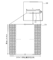
- FIG. 2 is a schematic plan view showing an example of the configuration of the mask 30 of the present embodiment.
- a rectangular mask portion 31 is formed on the mask 30.
- the dimension of the mask portion 31 in the scanning direction (vertical direction) is W, and the dimension in the direction orthogonal to the scanning direction (horizontal direction) is L.
- the mask unit 31 is provided with microlenses 21 in an array at equal intervals in the scanning direction and in the direction orthogonal to the scanning direction.
- An opening which will be described later, is formed at the center position of each microlens 21 in plan view.
- the vertical dimension W of the mask portion 31 can be, for example, about 5 mm, and the horizontal dimension L can be about 37 mm, but each dimension is not limited to these numerical values.
- Twenty macro lenses 21 are arranged at equal intervals in the scanning direction (vertical direction). Since one aperture corresponds to one macro lens 21, the mask 30 has 20 apertures formed at equal intervals in the scanning direction (vertical direction).
- FIG. 3 is a schematic diagram showing the positional relationship between the opening 32 and the microlens 21 of the present embodiment.
- FIG. 3 shows the positional relationship between the opening 32 and the microlens 21 in a front view, and shows the position of the opening 32 in a plan view on the basis of the position of the microlens 21 corresponding to the opening 32.
- the size of the opening 32 and the size of the irradiation pattern are described equivalently.
- the size of the part 32 is larger than the size of the irradiation pattern.
- the mask portion 31 has a plurality of openings 32 and microlenses (lenses) 21.
- the microlens 21 is formed on the transparent substrate 20 corresponding to the opening 32, and the transparent substrate 20 and the mask 30 are integrated.
- a rectangular opening 32 is arranged at the center of the microlens 21 that is circular in plan view.
- the mask 30 and the incident surface of the microlens 21 are spaced apart by an appropriate length.
- the maximum size (circular diameter in plan view) of the microlens 21 can be, for example, about 150 ⁇ m to 400 ⁇ m, but is not limited to these numerical values.
- the plurality of formed microlenses 21 is also referred to as a microlens array.
- the laser light that has passed through the opening 32 is condensed by the microlens 21, and the condensed laser light is A required portion on the substrate 10 is partially irradiated corresponding to each of the plurality of openings 32 (that is, the microlens 21).
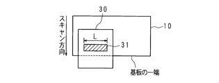
- FIG. 4A shows a state in which the mask 30 is set at a predetermined position, and shows a state before the movement of the substrate 10 in the scanning direction is started. From the state shown in FIG. 4A, the substrate 10 is moved in the scanning direction at a constant speed.
- the laser light source 50 irradiates laser light at time intervals at which the irradiation position of the substrate 10 reaches a position corresponding to the opening 32. For example, in the case of the opening 32 illustrated in FIG. 2, the same portion of the substrate 10 is irradiated with the laser light 20 times.
- FIG. 4A shows a state in which the mask 30 is set at a predetermined position, and shows a state before the movement of the substrate 10 in the scanning direction is started. From the state shown in FIG. 4A, the substrate 10 is moved in the scanning direction at a constant speed.
- the laser light source 50 irradiates laser light at time intervals at which the irradiation position of the substrate 10 reaches a position corresponding to the opening 32
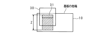
- FIG. 4B shows a state in which the substrate 10 is moved at a constant speed and moved to the final position in the scanning direction (by the distance Z).
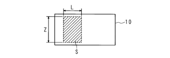
- the substrate 10 By moving the substrate 10 to the state shown in FIG. 4B, it is possible to partially irradiate a laser beam to a required portion within the irradiation region S of the substrate 10 as shown in FIG. 4C.
- the mask 30 In the state shown in FIG. 4C, the mask 30 is moved by a distance L in the direction orthogonal to the scanning direction, and the substrate 10 is moved in the scanning direction in the same manner as shown in FIGS. 4A and 4B, thereby increasing the irradiation region S. be able to.
- the size of the substrate 10 and the size of the mask 30 are shown to be approximately the same, but the size of the substrate 10 is actually much larger than that in FIG. 4.
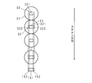
- FIG. 5 is a schematic diagram showing a first example of the opening 32 of the mask 30 of the present embodiment. In the following, both are shown so that the positional relationship between the opening 32 and the microlens 21 can be understood, and for convenience, only one row along the scanning direction is shown.
- (M + N) openings 32 are arranged at predetermined intervals in the scanning direction. All (M + N) openings 32 have first opening regions 321 that are aligned at equal intervals along the scanning direction and have the same shape.
- the center of the position of the first opening area 321 corresponds to the center of the microlens 21, and the shape of the first opening area 321 is rectangular.
- N openings 32 have a second opening region 322 connected to the first opening region 321 in a predetermined direction with respect to the first opening region 321.
- the predetermined direction is a direction orthogonal to the scan direction.
- the predetermined direction is not limited to this, and may be a scanning direction.
- the N openings 32 are connected to a pair of second opening regions 322 and 322 in a direction orthogonal to the scanning direction with the first opening region 321 interposed therebetween.
- the same portion of the substrate 10 is scanned with (N + M) times of laser light through the opening 32 having the first opening region 321 in one cycle of scanning, and the first opening region 321 and Laser light is irradiated N times through the opening having both of the second opening regions 322.
- the number of the plurality of openings 32 is (N + M), and the number of some of the openings 32 is N.
- the substrate 10 is moved at a constant speed along the scanning direction.
- the laser light source 50 irradiates laser light at time intervals at which the irradiation position of the substrate 10 reaches a position corresponding to the opening 32.
- the same portion of the substrate 10 is irradiated with (N + M) times of laser light in one cycle of scanning.
- a required portion of the substrate 10 corresponding to the first opening region 321 includes 1
- the laser beam is irradiated (N + M) times in the cycle scan.
- a required portion of the substrate 10 corresponding to the second opening region 322 is irradiated with N times of laser light in one cycle scan.
- the portion 151 corresponding to the first opening region 321 of the substrate 10 can increase the amount of laser light irradiation and increase the electron mobility, and is located at a position in a predetermined direction with respect to the first opening region 321.
- the portion 152 corresponding to the second opening region 322 connected to the opening region 321 can reduce the irradiation amount of the laser light and prevent the electron mobility from increasing too much. As a result, annealing treatment with partially different electron mobility can be performed in one cycle scan, and crystalline semiconductor films with different electron mobility can be formed.
- a part of the plurality of openings 32 includes a pair of second opening regions 322 that are connected to the first opening region 321 with the first opening region 321 interposed therebetween in a predetermined direction with respect to the first opening region 321.
- a pair of second opening regions 322 and 323 are arranged in a predetermined direction with the first opening region 321 interposed therebetween.
- a crystalline semiconductor film arranged in a predetermined direction in the order of a region 152 having a relatively high electron mobility, a region 151 having a large electron mobility, and a region 152 having a relatively large electron mobility is formed in one cycle of scanning. Can do.
- the size of the opening 32 (the first opening region 321 and the second opening region 322, 323) and the irradiation pattern (the first opening region 321 and the second opening region 322 of the substrate 10).
- the size of the opening 32 is larger than the size of the irradiation pattern because the laser light is actually condensed by the microlens 21. Is also big. The same applies to FIG. 6 and subsequent figures.
- FIG. 6 is a schematic view showing the main part of a thin film transistor annealed by the laser annealing apparatus 100 of this embodiment
- FIG. 7 is a side view of the thin film transistor annealed by the laser annealing apparatus 100 of this embodiment. It is a schematic diagram which shows the principal part. 6 and 7, only the main part is shown for simplicity.
- the thin film transistor annealed by the laser annealing apparatus 100 of the present embodiment includes the gate electrode 11 formed on the surface of the substrate 10, and the gate electrode 11.
- FIG. 8 is a schematic diagram showing a main part of an ideal thin film transistor annealed by a conventional laser annealing apparatus.
- the upper part of FIG. 8 shows openings provided corresponding to the lenses, and the shapes of the openings are all the same.
- 8 shows the main part of the thin film transistor in plan view
- the lower part of FIG. 8 shows the main part of the thin film transistor in side view.
- a portion of the substrate corresponding to the opening corresponds to a gap between the source electrode 12 and the drain electrode 13.
- a gap between the source electrode 12 and the drain electrode 13 is formed by the crystalline semiconductor film 15, and is directly below the source electrode 12 and the drain electrode 13. Is formed of an amorphous semiconductor film 14. With this configuration, the leakage current can be reduced and the drive current can be increased.
- FIG. 9 is a schematic view showing a main part of an example of a conventional thin film transistor.
- the shapes of the openings formed in the mask are all the same.
- a portion of the substrate corresponding to the opening is a gap between the source electrode 12 and the drain electrode 13.
- the region irradiated with the laser light may deviate from the gap part due to a positional deviation when the substrate 10 is transported in the scanning direction or a deviation of the optical axis of the laser light.
- a part of the amorphous semiconductor film 14 is formed.
- the electron mobility in a part of the gap portion becomes small, and the driving current cannot be increased.
- FIG. 10 is a schematic diagram showing the main part of another example of a thin film transistor annealed by a conventional laser annealing apparatus.
- the opening shown in FIG. 10 has a lateral dimension so that a part of the source electrode 12 and the part of the drain electrode 13 are also irradiated with laser light. Is slightly longer.
- the gap between the source electrode 12 and the drain electrode 13 is always in the crystalline semiconductor film 15. Formed with.
- a region immediately below a part of each of the source electrode 12 and the drain electrode 13 is also formed of the crystalline semiconductor film 15, so that there is a disadvantage that leakage current increases.
- the portion 151 corresponding to the first opening region 321 of the substrate 10 can increase the amount of laser light irradiation and increase the electron mobility, and the first opening region 321.
- the portion 152 corresponding to the second opening region 322 connected to the first opening region 321 at a position in a predetermined direction can reduce the irradiation amount of the laser light and prevent the electron mobility from increasing too much. .
- annealing treatment with partially different electron mobility can be performed in one cycle scan, and crystalline semiconductor films with different electron mobility can be formed.
- the gap between the source electrode 12 and the drain electrode 13 is formed of a crystalline semiconductor film 15 having a high electron mobility. Since the crystalline semiconductor film 15 having a relatively high electron mobility is formed immediately below a part of each of the drain electrode 13 and the drain electrode 13, a leakage current can be reduced and a driving current can be increased.
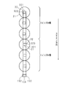
- FIG. 11 is a schematic diagram showing a second example of the opening 32 of the mask 30 of the present embodiment.
- the difference from the first embodiment shown in FIG. 5 is that, in the second embodiment, the opening 32 having only the first opening region 321 and the opening having both the first opening region 321 and the second opening region 322. 32 are alternately arranged along the scanning direction. By arranging them alternately, variations such as unevenness in incident light and shift in transport of the substrate 10 are diffused (averaged), and a thin film transistor having uniform characteristics can be manufactured.
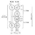
- FIG. 12 is a schematic diagram showing a third example of the opening 32 of the mask 30 of the present embodiment.
- the type of the opening 32 differs depending on the row of the openings 32 arranged in the scanning direction.
- the first row is constituted by the same row of openings 32 as in the first embodiment, and in the second row, all (M + N) openings 32 have only the first opening region 321.
- crystalline semiconductor films having different modes of electron mobility can be formed in one cycle of scanning.
- FIG. 13 is a schematic diagram showing a fourth example of the opening 32 of the mask 30 of the present embodiment.
- all (M + N) openings 32 have first opening regions 321 that are aligned at equal intervals along the scanning direction and have the same shape.
- the center of the position of the first opening area 321 corresponds to the center of the microlens 21, and the shape of the first opening area 321 is rectangular.
- N openings 32 have a second opening region 323 connected to the first opening region 321 in a predetermined direction with respect to the first opening region 321.
- the predetermined direction is a direction orthogonal to the scan direction.
- K openings 32 have a second opening region 322 at a position facing the second opening region 323 across the first opening region 321.
- the substrate portion 151 corresponding to the first opening region 321 is irradiated with (M + N) times of laser light
- the substrate portion 152 corresponding to the second opening region 323 is irradiated with N times of laser light.
- the substrate portion 153 corresponding to the second opening region 322 is irradiated with K times of laser light.
- FIG. 14 is a schematic diagram showing a fifth example of the opening 32 of the mask 30 of the present embodiment.
- all (M + N) openings 32 have first opening regions 321 that are aligned at equal intervals along the scanning direction and have the same shape.
- the center of the position of the first opening area 321 corresponds to the center of the microlens 21, and the shape of the first opening area 321 is rectangular.
- M openings 32 have a second opening region 322 connected to the first opening region 321 in a predetermined direction with respect to the first opening region 321.
- the predetermined direction is a direction orthogonal to the scan direction.
- the second opening region 322 is provided on the left side of the first opening region 321.
- N openings 32 have second opening regions 323 connected to the first opening regions 321 in a predetermined direction with respect to the first opening regions 321.
- the second opening region 323 is provided on the right side of the first opening region 321.
- the shape and size of each of the (M + N) openings 32 are the same, and the positions of the M openings 32 are shifted to the left from the center. Further, the positions of the N openings 32 are shifted from the center to the right side.
- the substrate portion 151 corresponding to the first opening region 321 is irradiated with (M + N) times of laser light
- the substrate portion 152 corresponding to the second opening region 322 is irradiated with M times of laser light.
- the substrate portion 152 corresponding to the second opening region 323 is irradiated with laser light N times. Accordingly, crystalline semiconductor films having different electron mobilities can be formed in one cycle of scanning.
- the predetermined direction is a direction orthogonal to the scanning direction
- the first opening region 321 and the second opening regions 322 and 323 have the same dimensions in the scanning direction.
- the crystalline semiconductor film having the same dimension in the scanning direction and the electron mobility being relatively large, large, and relatively large and arranged along the direction orthogonal to the scanning direction is formed. Can do.
- FIG. 15 is a schematic view showing a sixth example of the opening 32 of the mask 30 of the present embodiment.
- all (M + N) openings 32 have first opening regions 321 that are aligned at equal intervals along the scanning direction and have the same shape.
- the center of the position of the first opening area 321 corresponds to the center of the microlens 21, and the shape of the first opening area 321 is rectangular.
- N openings 32 are a set of second openings that are connected to the first opening area 321 with the first opening area 321 in the scanning direction with respect to the first opening area 321. Open regions 324 and 325 are provided. In other words, the N openings 32 have a pair of second opening regions 324 and 325 in the scanning direction with the first opening region 321 interposed therebetween.
- the portion 151 corresponding to the first opening region 321 of the substrate 10 can increase the amount of laser light irradiation and increase the electron mobility.
- the portion 152 corresponding to the second opening regions 324 and 325 It is possible to prevent the irradiation amount from decreasing and the electron mobility from increasing too much. As a result, annealing treatment with partially different electron mobility can be performed in one cycle scan, and crystalline semiconductor films with different electron mobility can be formed.
- FIG. 16 is a schematic diagram showing a seventh example of the opening 32 of the mask 30 of the present embodiment.
- all (M + N) openings 32 have first opening regions 321 that are aligned at equal intervals along the scanning direction and have the same shape.
- the center of the position of the first opening area 321 corresponds to the center of the microlens 21, and the shape of the first opening area 321 is rectangular.
- the M openings 32 have a second opening region 324 connected to the first opening region 321 in the scanning direction with respect to the first opening region 321.
- the second opening region 324 is provided above the first opening region 321.
- N openings 32 have a second opening region 325 connected to the first opening region 321 in the scanning direction with respect to the first opening region 321.
- a second opening region 325 is provided below the first opening region 321.
- the shape and size of each of the (M + N) openings 32 are the same, and the positions of the M openings 32 are shifted upward from the center (backward in the scanning direction). Further, the positions of the N openings 32 are shifted from the center to the lower side (forward in the scanning direction).
- the substrate portion 151 corresponding to the first opening region 321 is irradiated with (M + N) times of laser light
- the substrate portion 152 corresponding to the second opening region 324 is irradiated with M times of laser light.
- the portion 152 of the substrate corresponding to the second opening region 325 is irradiated with laser light N times. Accordingly, crystalline semiconductor films having different electron mobilities can be formed in one cycle of scanning.
- the predetermined direction is the scanning direction
- the dimensions of the first opening region 321 and the second opening regions 324 and 325 in the direction orthogonal to the scanning direction are the same. is there.
- a crystalline semiconductor film is formed in which the dimensions in the direction orthogonal to the scanning direction are the same and the electron mobility is relatively large, large, and relatively large, arranged in the order of the scanning direction. Can do.
- the first opening region 321 has a rectangular shape. Since the first opening region 321 has a rectangular shape, a portion of the substrate corresponding to the first opening region 321 can be a gap portion between the source electrode 12 and the drain electrode 13. Further, the second opening regions 322, 323, 324, and 325 connected to the first opening region 321 can be portions directly below the electrodes of the source electrode 12 and the drain electrode 13.
- the laser annealing apparatus 100 of the present embodiment includes the microlens 21 that condenses the laser light, it is possible to partially irradiate the laser beam to a required portion of the substrate and perform partial laser annealing. Moreover, since the laser annealing apparatus 100 of this Embodiment is provided with the laser light source 50, it can perform partial laser annealing.
- FIG. 17 is a schematic diagram showing an eighth example of the opening 32 of the mask 30 of the present embodiment.
- the opening 32 is provided with minute rectangular adjustment members 35 arranged in a lattice pattern.
- the adjusting member 35 is for adjusting the amount of laser beam irradiation, and any suitable material can be used as long as it is made of a material that reduces the amount of laser beam transmission.
- the pattern B the position of the adjustment member 35 of the pattern A is opened, and the adjustment member 35 is provided at the position where the pattern A is opened.
- the positions of the adjustment members 35 complement each other, so that the unevenness of the amount of laser light irradiation can be made uniform.
- the electron mobility of the crystalline semiconductor layer can be adjusted to a required value by adjusting the amount of laser light applied to a required portion of the substrate 10 in one cycle of scanning.
- FIG. 18 is a schematic diagram showing a ninth example of the opening 32 of the mask 30 of the present embodiment.
- the opening 32 is provided with a minute rectangular adjustment member 36 arranged in a slit shape.
- the position of the adjustment member 36 of the pattern C is opened, and the adjustment member 36 is provided in the opening position of the pattern C.
- the position of the adjusting member 36 that adjusts the laser beam irradiation amount is set to a complementary position so that the laser beam irradiation amount can be made uniform and uniform.
- the electron mobility of the crystalline semiconductor layer can be adjusted to a required value by adjusting the amount of laser light applied to a required portion of the substrate 10 in one cycle of scanning.
- the opening 32 as shown in FIGS. 17 and 18 may be applied to the opening 32 having only the first opening region 321, or the first opening region 321 and the second opening regions 322, 323, 324, 325. It can also be applied to the opening 32 having both of the above. 17 and 18 may be applied to both the first opening region 321 and the second opening regions 322, 323, 324, and 325, or the first opening region 321 and the second opening region 321 You may apply only to either one of 2 opening area
- FIG. 19 is a flowchart showing an example of a laser annealing method using the laser annealing apparatus 100 of the present embodiment.
- the laser annealing apparatus 100 is referred to as an apparatus 100 for the sake of simplicity.
- the apparatus 100 sets the mask 30 at a predetermined position (S11), and irradiates laser light (S12).
- the apparatus 100 moves the substrate 10 in the scanning direction at a constant speed (S13).
- the laser light source 50 irradiates laser light at time intervals at which the irradiation position of the substrate 10 reaches a position corresponding to the opening 32 of the mask 30.
- the apparatus 100 determines whether or not the substrate 10 has been moved to the final position in the scanning direction (S14). If the substrate 10 has not been moved to the final position (NO in S14), the processing from step S12 is repeated. When the substrate 10 is moved to the final position in the scanning direction (YES in S14), the apparatus 100 determines whether or not the laser light irradiation of a predetermined area of the substrate 10 is completed (S15).
- the apparatus 100 moves the mask 30 by a predetermined distance (a dimension L in the lateral direction of the mask 30) in a direction orthogonal to the scanning direction. (S16), the process after step S12 is repeated.
- the apparatus 100 ends the process.
- the substrate 10 is moved (conveyed) in the scanning direction.
- the present invention is not limited to this, and the substrate 10 is fixed and the mask 30 (including the optical system 40 is included). May be moved in the scanning direction.
- the shape of the opening 32 is rectangular, but the shape of the opening 32 is not limited to a rectangular shape, and may be, for example, an elliptical shape. Further, circular or rectangular cutouts may be provided at the four corners of the rectangular opening 32. Thereby, the irradiation amount of the laser light near the four corners of the opening 32 can be slightly increased, and the shape of the region irradiated with the laser light can be made rectangular.
- This embodiment can be applied not only to a TFT using a silicon semiconductor but also to a TFT using an oxide semiconductor, and can perform an annealing process with partially different electron mobility in one cycle scan.
- a laser annealing apparatus is a laser annealing apparatus that includes a mask having a plurality of openings formed along a scanning direction, and irradiates a substrate with laser light through the openings.
- the plurality of openings have first opening regions that are aligned along the scanning direction and have the same shape, and some of the openings are in a predetermined direction with respect to the first opening region. It has the 2nd opening area
- the mask according to the embodiment of the present invention is a mask in which a plurality of openings are formed along the scanning direction of the substrate, and the plurality of openings are aligned along the scanning direction and have the same shape. It has a 1st opening area
- a thin film transistor includes a gate electrode formed on a surface of a substrate, an amorphous semiconductor film formed above the gate electrode, and the amorphous semiconductor film.
- the source electrode, the drain electrode formed on the amorphous semiconductor film, and the amorphous semiconductor film directly below a part of each of the source electrode and the drain electrode among the amorphous semiconductor films are described above.
- the crystalline semiconductor film formed by annealing with the laser annealing apparatus according to the embodiment, and the amorphous semiconductor film between the source electrode and the drain electrode among the amorphous semiconductor film is formed as described above.
- a laser annealing method is a laser annealing method using the laser annealing apparatus according to any one of the present embodiments, the relative position of the substrate and the mask is moved along the scanning direction, The substrate is irradiated with laser light through a plurality of openings formed in the mask.
- the mask has a plurality of openings along the scanning direction of the substrate.
- the openings can be formed at predetermined intervals, for example.
- the plurality of openings have first opening regions aligned along the scanning direction and having the same shape.
- Some of the plurality of openings have a second opening region connected to the first opening region in a predetermined direction with respect to the first opening region.
- the predetermined direction can be a direction orthogonal to the scan direction, but is not limited thereto, and may be the scan direction.
- the number of the plurality of openings is (N + M), and the number of some of the openings is N.
- the substrate is moved at a constant speed along the scanning direction, and the laser beam is irradiated at a time interval at which the irradiation position of the substrate reaches a position corresponding to the opening. (N + M) times of laser light is irradiated. Since the plurality of openings have the first opening region that is aligned along the scanning direction and has the same shape, the required portion of the substrate corresponding to the first opening region is (N + M) times in one cycle of scanning. The laser beam is irradiated. Further, a required portion of the substrate corresponding to the second opening region is irradiated with N times of laser light in one cycle scan. Note that the first opening regions can be aligned at equal intervals along the scanning direction, for example.
- the portion corresponding to the first opening region of the substrate can increase the amount of laser light irradiation and increase the electron mobility, and is located in a predetermined direction with respect to the first opening region.
- the portion corresponding to the second opening region connected to the region can reduce the irradiation amount of the laser light so that the electron mobility does not increase too much.
- annealing treatment with partially different electron mobility can be performed in one cycle scan, and crystalline semiconductor films with different electron mobility can be formed.
- a part of the plurality of openings has the first opening region with the first opening region in the predetermined direction with respect to the first opening region. And a pair of second opening regions connected to each other.
- Some of the plurality of openings have a pair of second opening regions that are connected to the first opening region with the first opening region in a predetermined direction with respect to the first opening region. That is, a pair of second opening regions are arranged in a predetermined direction with the first opening region interposed therebetween.
- crystalline semiconductor films arranged in a predetermined direction in the order of relatively high electron mobility and relatively large electron mobility can be formed in one cycle scan.
- the predetermined direction is a direction orthogonal to the scanning direction, and the first opening region and the second opening region have the same dimension in the scanning direction. It is characterized by.
- the predetermined direction is a direction orthogonal to the scanning direction, and the dimensions of the first opening region and the second opening region in the scanning direction are the same.
- the crystalline semiconductor film having the same dimension in the scanning direction and the electron mobility being relatively large, large, and relatively large and arranged along the direction orthogonal to the scanning direction is formed. Can do.
- the predetermined direction is the scanning direction
- the first opening region and the second opening region have the same dimensions in a direction perpendicular to the scanning direction. It is characterized by.
- the predetermined direction is the scanning direction, and the dimensions of the first opening region and the second opening region in the direction orthogonal to the scanning direction are the same.
- a crystalline semiconductor film is formed in which the dimensions in the direction orthogonal to the scanning direction are the same and the electron mobility is relatively large, large, and relatively large, arranged in the order of the scanning direction. Can do.
- the laser annealing apparatus is characterized in that the first opening region has a rectangular shape.
- the first opening area has a rectangular shape. Since the first opening region has a rectangular shape, a portion of the substrate corresponding to the first opening region can be a gap portion between the source electrode and the drain electrode. In addition, the second opening region connected to the first opening region can be a portion directly below the electrodes directly below a part of each of the source electrode and the drain electrode.
- the laser annealing apparatus is characterized in that all or a part of the plurality of openings includes an adjustment member that adjusts an irradiation amount of laser light.
- All or some of the plurality of openings are provided with an adjustment member that adjusts the amount of laser beam irradiation.
- an appropriate material can be used for the adjustment member as long as it is made of a material that reduces the amount of laser light transmitted.
- the adjustment member may be provided with a lattice-like or linear slit in the first opening region of the opening, or may be provided with a lattice-like or linear slit in the first opening region and the second opening region of the opening. . Accordingly, the electron mobility of the crystalline semiconductor layer can be adjusted to a required value by adjusting the irradiation amount of the laser light irradiated to the required portion of the substrate in one cycle of scanning.
- the laser annealing apparatus includes a lens that is provided in each of the plurality of openings, and that condenses the laser light irradiated through the openings.
- a laser annealing apparatus includes a laser light source that emits laser light irradiated through each of the plurality of openings.
Landscapes
- Physics & Mathematics (AREA)
- Optics & Photonics (AREA)
- Engineering & Computer Science (AREA)
- Plasma & Fusion (AREA)
- Mechanical Engineering (AREA)
- Recrystallisation Techniques (AREA)
- Thin Film Transistor (AREA)
- Electromagnetism (AREA)
Abstract
部分的に電子移動度が異なるアニール処理を行うことができるレーザーアニール装置、マスク、薄膜トランジスタ及びレーザーアニール方法を提供する。 スキャン方向に沿って複数の開口部が形成されたマスクを備え、基板をスキャン方向に移動させ、開口部を介してレーザー光を基板に照射するレーザーアニール装置であって、複数の開口部は、スキャン方向に沿って整列し形状が同一の第1開口領域を有し、複数の開口部のうち一部の開口部は、第1開口領域に対する所定方向に第1開口領域と繋がる第2開口領域を有する。
Description
本発明は、マスクに形成された開口部を介してレーザー光を基板に照射するレーザーアニール装置、該レーザーアニール装置を構成するマスク、該レーザーアニール装置によりレーザーアニールされた薄膜トランジスタ及び前記レーザーアニール装置を用いるレーザーアニール方法に関する。
TFT(Thin Film Transistor:薄膜トランジスタ)方式の液晶ディスプレイは、TFT基板とR(赤)、G(緑)、B(青)の色を有するカラーフィルタ基板とを所要の隙間を設けて貼り合わせ、TFT基板とカラーフィルタ基板との間に液晶を注入し、液晶分子による光の透過率を画素毎に制御することにより、映像を表示することができる。
TFT基板には、データ線及び走査線が縦横方向に格子状に配線され、データ線と走査線とが交差する箇所にTFTで構成される画素を形成してある。また、複数の画素で構成される表示領域の周囲には、TFTで構成されデータ線及び走査線を駆動する駆動回路を形成してある。
TFTとしては、例えば、シリコン半導体を用いたアモルファスシリコン(非晶質、a-Si)TFT、半導体層をポリシリコン(多結晶、p-Si)とした低温ポリシリコンTFTなどの開発が行われている。a-SiTFTは、抵抗が高く漏れ電流(リーク電流)が小さい。また、p-SiTFTは、a-SiTFTに比べて電子の移動度が格段に大きい。
アモルファスシリコン層にレーザー光を照射してアニール処理をすることによりポリシリコン層にすることができる。例えば、レーザー光源から出射されたレーザー光をレンズ群により平行ビームに成形し、成形した平行ビームを開口部が形成された遮光部材及びマイクロレンズアレイを介して基板に照射するレーザーアニール装置がある。このようなレーザーアニール装置では、遮光部材には基板のスキャン方向に沿って所定数の開口部が配置され、基板を開口部のピッチだけ移動させる都度、レーザー光を照射することにより、1サイクルのスキャンで基板の所要箇所には開口部の数に等しい回数だけレーザー光が照射されるので、同じ照射量のレーザー光を照射することができる(特許文献1参照)。
しかし、従来のレーザーアニール装置は、1サイクルのスキャンで同じ照射量のレーザー光が基板の所要箇所に照射される。このため、例えば、ソース電極及びドレイン電極間のギャップ部分、並びにソース電極及びドレイン電極それぞれの一部の直下の電極直下部分を所要箇所とした場合、ギャップ部及び電極直下部分それぞれのポリシリコン層の電子移動度が同じように高くなり、TFTの漏れ電流が大きくなる。
本発明は斯かる事情に鑑みてなされたものであり、部分的に電子移動度が異なるアニール処理を行うことができるレーザーアニール装置、該レーザーアニール装置を構成するマスク、該レーザーアニール装置によりレーザーアニールされた薄膜トランジスタ及び前記レーザーアニール装置を用いるレーザーアニール方法を提供することを目的とする。
本発明の実施の形態に係るレーザーアニール装置は、スキャン方向に沿って複数の開口部が形成されたマスクを備え、前記開口部を介してレーザー光を基板に照射するレーザーアニール装置であって、前記複数の開口部は、前記スキャン方向に沿って整列し形状が同一の第1開口領域を有し、前記複数の開口部のうち一部の開口部は、前記第1開口領域に対する所定方向に該第1開口領域と繋がる第2開口領域を有することを特徴とする。
本発明の実施の形態に係るマスクは、基板のスキャン方向に沿って複数の開口部が形成されたマスクであって、前記複数の開口部は、前記スキャン方向に沿って整列し形状が同一の第1開口領域を有し、前記複数の開口部のうち一部の開口部は、前記第1開口領域に対する所定方向に該第1開口領域と繋がる第2開口領域を有することを特徴とする。
本発明の実施の形態に係る薄膜トランジスタは、薄膜トランジスタにおいて、基板の表面に形成されたゲート電極と、該ゲート電極の上側に形成された非晶質半導体膜と、該非晶質半導体膜上に形成されたソース電極と、前記非晶質半導体膜上に形成されたドレイン電極と、前記非晶質半導体膜のうち、前記ソース電極及びドレイン電極それぞれの一部の直下の前記非晶質半導体膜を前述の実施の形態に係るレーザーアニール装置でアニール処理して形成された直下結晶性半導体膜と、前記非晶質半導体膜のうち、前記ソース電極及びドレイン電極間の前記非晶質半導体膜を前述の実施の形態に係るレーザーアニール装置でアニール処理して形成された電極間結晶性半導体膜とを備え、前記電極間結晶性半導体膜の電子移動度が前記直下結晶性半導体膜の電子移動度より高いことを特徴とする。
本発明の実施の形態に係るレーザーアニール方法は、前述の実施の形態に係るレーザーアニール装置を用いるレーザーアニール方法であって、基板及びマスクの相対位置をスキャン方向に沿って移動させ、マスクに形成された複数の開口部を介してレーザー光を前記基板に照射することを特徴とする。
本発明によれば、部分的に電子移動度が異なるアニール処理を行うことができる。
以下、本発明をその実施の形態を示す図面に基づいて説明する。図1は本実施の形態のレーザーアニール装置100の構成の一例を示す模式図である。本実施の形態のレーザーアニール装置100は、レーザー光を出射するレーザー光源50、レーザー光源50から出射されたレーザー光を平行ビームに成形するためのレンズ群を含む光学系40、後述の開口部及びマイクロレンズがアレイ状に配置されたマスク部31を有するマスク(遮光板)30などを備える。光学系40で成形された平行ビームは、マスク部31に設けられた開口部及びマイクロレンズを介して基板10の所要箇所に部分的に照射される。また、基板10は不図示の駆動機構により一定の速度で搬送される。レーザー光源50は、基板10の照射位置が開口部に対応する位置に到達する時間間隔でレーザー光を照射する。なお、レーザーアニール装置100は、基板10を移動させる構成に代えて、基板10を固定しておき、マスク30を移動させる構成であってもよい。以下では、基板10を移動させる例について説明する。
図2は本実施の形態のマスク30の構成の一例を示す平面視の模式図である。マスク30には、矩形状のマスク部31を形成してある。マスク部31のスキャン方向(縦方向)の寸法をWとし、スキャン方向と直交する方向(横方向)の寸法をLとする。マスク部31には、スキャン方向及びスキャン方向と直交する方向それぞれに等間隔でアレイ状にマイクロレンズ21が設けられている。それぞれのマイクロレンズ21の平面視での中心位置には、後述の開口部を形成してある。
マスク部31の縦方向の寸法Wは、例えば、約5mmとすることができ、横方向の寸法Lは、約37mmとすることができるが、各寸法はこれらの数値に限定されない。マクロレンズ21は、スキャン方向(縦方向)に20個等間隔で並べてある。1個のマクロレンズ21には、1個の開口部が対応するので、マスク30は、スキャン方向(縦方向)に20個等間隔で開口部を形成してある。
図3は本実施の形態の開口部32及びマイクロレンズ21の位置関係を示す模式図である。図3は正面視での開口部32及びマイクロレンズ21の位置関係を示すとともに、平面視で開口部32の位置を当該開口部32に対応するマイクロレンズ21の位置を基準にして示す。なお、本実施の形態では、簡便のため、開口部32の大きさと照射パターンの大きさとは同等に記載しているが、実際には、レーザー光がマイクロレンズ21により集光されるので、開口部32のサイズは照射パターンのサイズよりも大きい。図3に示すように、マスク部31は、複数の開口部32及びマイクロレンズ(レンズ)21を有する。なお、マイクロレンズ21は、開口部32に対応して透明基板20上に形成されており、透明基板20とマスク30とは一体的になっている。また、平面視が円形のマイクロレンズ21の中心に矩形状の開口部32を配置してある。また、マスク30とマイクロレンズ21の入射面とは、適長離隔して配置されている。マイクロレンズ21の最大サイズ(平面視の円形の直径)は、例えば、150μm~400μm程度とすることができるが、これらの数値に限定されない。複数形成されたマイクロレンズ21をマイクロレンズアレイとも称する。
前述の光学系40で成形された平行ビームがマスク部31の開口部32に照射されると、開口部32を通過したレーザー光は、マイクロレンズ21で集光され、集光されたレーザー光が、複数の開口部32(すなわち、マイクロレンズ21)それぞれに対応して基板10上の所要箇所に部分的に照射される。
図4A、図4B及び図4Cは本実施の形態のレーザーアニール装置100による基板10のスキャンの一例を示す模式図である。図4Aは、マスク30が所定位置にセットされた状態を示し、基板10のスキャン方向の移動が開始される前の状態を示す。図4Aに示す状態から、基板10をスキャン方向に一定の速度で移動させる。レーザー光源50は、基板10の照射位置が開口部32に対応する位置に到達する時間間隔でレーザー光を照射する。例えば、図2に例示した開口部32の場合、基板10の同じ個所には、20回レーザー光が照射されることになる。図4Bは、基板10を一定の速度で移動させて、スキャン方向の最終位置まで(距離Zだけ)移動した状態を示す。基板10を図4Bに示す状態まで移動させることにより、図4Cに示すように、基板10の照射領域Sの範囲内の所要箇所にレーザー光を部分照射することができる。図4Cに示す状態で、マスク30をスキャン方向と直交する方向に距離Lだけ移動させ、図4A及び図4Bに示す場合と同様に基板10をスキャン方向に移動させることにより、照射領域Sを増やすことができる。なお、図4では、基板10のサイズとマスク30のサイズを同程度に図示しているが、実際は基板10のサイズは、図4の場合よりも遥かに大きい。
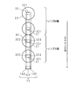
次に、本実施の形態のマスク30の開口部32の詳細について説明する。図5は本実施の形態のマスク30の開口部32の第1実施例を示す模式図である。なお、以下では、開口部32とマイクロレンズ21との位置関係が分かるように両者を図示するとともに、簡便のため、スキャン方向に沿った1列だけを図示している。
図5に示すように、第1実施例では、(M+N)個の開口部32がスキャン方向に所定間隔で配置されている。(M+N)個すべての開口部32は、スキャン方向に沿って等間隔で整列し形状が同一の第1開口領域321を有する。第1開口領域321の位置の中心はマイクロレンズ21の中心に対応し、第1開口領域321の形状は矩形状である。
また、(M+N)個のうち、N個の開口部32は、第1開口領域321に対する所定方向に第1開口領域321と繋がる第2開口領域322を有する。以下の例では、所定方向は、スキャン方向と直交する方向であるとして説明する。なお、所定方向は、これに限定されず、スキャン方向であってもよい。図5の例では、N個の開口部32は、第1開口領域321を挟んでスキャン方向と直交する方向に1組の第2開口領域322、322が繋がっている。
第1実施例の場合、1サイクルのスキャンで基板10の同じ個所には、第1開口領域321を有する開口部32を介して、(N+M)回レーザー光が照射され、第1開口領域321及び第2開口領域322の両方を有する開口部を介して、N回レーザー光が照射される。
すなわち、複数の開口部32の数を(N+M)とし、一部の開口部32の数をNとする。基板10をスキャン方向に沿って一定の速度で移動させる。レーザー光源50は、基板10の照射位置が開口部32に対応する位置に到達する時間間隔でレーザー光を照射する。これにより、1サイクルのスキャンで基板10の同じ個所には、(N+M)回のレーザー光が照射される。そして、複数の開口部32それぞれは、スキャン方向に沿って等間隔で整列し形状が同一の第1開口領域321を有するので、第1開口領域321に対応する基板10の所要箇所には、1サイクルのスキャンで(N+M)回のレーザー光が照射される。また、第2開口領域322に対応する基板10の所要箇所には、1サイクルのスキャンでN回のレーザー光が照射される。
基板10の第1開口領域321に対応する箇所151は、レーザー光の照射量が多くなり電子移動度を大きくすることができ、第1開口領域321に対して所定方向の位置にあって第1開口領域321と繋がる第2開口領域322に対応する箇所152は、レーザー光の照射量が少なくなり電子移動度があまり大きくならないようにすることができる。これにより、1サイクルのスキャンで部分的に電子移動度が異なるアニール処理を行うことができ、電子移動度が異なる結晶性半導体膜を形成することができる。
また、複数の開口部32のうち一部の開口部32は、第1開口領域321に対する所定方向に第1開口領域321を間にして第1開口領域321と繋がる1組の第2開口領域322、323を有する。すなわち、第1開口領域321を挟んで1組の第2開口領域322、323が所定方向に配置されている。これにより、1サイクルのスキャンで、例えば、電子移動度が比較的大きい領域152、大きい領域151、及び比較的大きい領域152、の順序で所定方向に沿って並んだ結晶性半導体膜を形成することができる。なお、図5の例では、簡便のため、開口部32(第1開口領域321及び第2開口領域322、323)の大きさと照射パターン(基板10の第1開口領域321及び第2開口領域322、323に対応する箇所151、152)の大きさとは同等に記載しているが、実際には、レーザー光がマイクロレンズ21により集光されるので、開口部32のサイズは照射パターンのサイズよりも大きい。図6以降についても同様である。
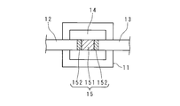
図6は本実施の形態のレーザーアニール装置100によりアニール処理した薄膜トランジスタの平面視の要部を示す模式図であり、図7は本実施の形態のレーザーアニール装置100によりアニール処理した薄膜トランジスタの側面視の要部を示す模式図である。なお、図6及び図7では、簡便のため要部のみを図示している。
図6及び図7に示すように、本実施の形態のレーザーアニール装置100によりアニール処理した薄膜トランジスタ(本実施の形態の薄膜トランジスタ)は、基板10の表面に形成されたゲート電極11と、ゲート電極11の上側に形成された非晶質半導体膜14と、非晶質半導体膜14上に形成されたソース電極12と、非晶質半導体膜14上に形成されたドレイン電極13と、非晶質半導体膜14のうち、ソース電極12及びドレイン電極13それぞれの一部の直下の非晶質半導体膜14をレーザーアニール装置100でアニール処理して形成された直下結晶性半導体膜152と、非晶質半導体膜14のうち、ソース電極12及びドレイン電極13間の非晶質半導体膜14をレーザーアニール装置199でアニール処理して形成された電極間結晶性半導体膜151とを備える。そして、電極間結晶性半導体膜151の電子移動度が直下結晶性半導体膜152の電子移動度より高い。
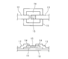
次に、比較例として従来の場合について説明する。図8は従来のレーザーアニール装置によりアニール処理された理想的な薄膜トランジスタの要部を示す模式図である。図8の上段の図は、レンズに対応して設けられた開口部であり、開口部の形状はすべて同じ形状となっている。図8の中段は、薄膜トランジスタの平面視の要部を示し、図8の下段は、薄膜トランジスタの側面視の要部を示す。開口部に対応する基板の箇所は、ソース電極12及びドレイン電極13間のギャップ部に相当する。図8に示すように、仮に理想的な薄膜トランジスタを作製できたとすると、ソース電極12及びドレイン電極13間のギャップ部は、結晶性半導体膜15で形成され、ソース電極12及びドレイン電極13それぞれの直下は非晶質半導体膜14で形成されている。かかる構成により、漏れ電流を少なくすることができるとともに、駆動電流を大きくすることができる。
図9は従来の薄膜トランジスタの一例の要部を示す模式図である。従来のレーザーアニール装置では、マスクに形成された開口部の形状はすべて同一である。また、開口部に対応する基板の箇所を、ソース電極12及びドレイン電極13間のギャップ部とする。基板10をスキャン方向へ搬送する際の位置ずれ、あるいはレーザー光の光軸のずれ等により、レーザー光が照射される領域がギャップ部からずれる場合があり、図9に示すように、ギャップ部の一部が非晶質半導体膜14で形成されてしまう。図9に示すような薄膜トランジスタでは、ギャップ部の一部の電子移動度が小さくなり、駆動電流を大きくすることができない。
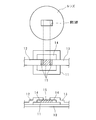
図10は従来のレーザーアニール装置によりアニール処理された薄膜トランジスタの他の例の要部を示す模式図である。図10に示す開口部は、図8に示す開口部に比べて、ソース電極12の直下の一部及びドレイン電極13の直下の一部にもレーザー光が照射されるように、横方向の寸法を若干長くしてある。これにより、基板10をスキャン方向へ搬送する際の位置ずれ、あるいはレーザー光の光軸のずれ等が発生した場合でも、ソース電極12及びドレイン電極13間のギャップ部は、必ず結晶性半導体膜15で形成される。しかし、図10に示すように、ソース電極12及びドレイン電極13それぞれの一部の直下の領域も結晶性半導体膜15で形成されるため、漏れ電流が大きくなるという欠点が生じる。
一方、前述のとおり、本実施の形態では、基板10の第1開口領域321に対応する箇所151は、レーザー光の照射量が多くなり電子移動度を大きくすることができ、第1開口領域321に対して所定方向の位置にあって第1開口領域321と繋がる第2開口領域322に対応する箇所152は、レーザー光の照射量が少なくなり電子移動度があまり大きくならないようにすることができる。これにより、1サイクルのスキャンで部分的に電子移動度が異なるアニール処理を行うことができ、電子移動度が異なる結晶性半導体膜を形成することができる。
また、図6及び図7に示すように、本実施の形態の薄膜トランジスタは、ソース電極12及びドレイン電極13間のギャップ部は、電子移動度の大きい結晶性半導体膜15で形成され、ソース電極12及びドレイン電極13それぞれの一部の直下は、電子移動度が比較的大きい結晶性半導体膜15で形成されているので、漏れ電流を少なくすることができるとともに、駆動電流を大きくすることができる。
図11は本実施の形態のマスク30の開口部32の第2実施例を示す模式図である。図5に示す第1実施例との相違点は、第2実施例では、第1開口領域321だけを有する開口部32と、第1開口領域321及び第2開口領域322の両方を有する開口部32とを、スキャン方向に沿って交互に配置してある。交互に配置することにより、入射光のムラ、基板10の搬送のズレ等のばらつきが拡散(平均化)され、特性が均一の薄膜トランジスタを製造することができる。
図12は本実施の形態のマスク30の開口部32の第3実施例を示す模式図である。図5に示す第1実施例との相違点は、第3実施例では、スキャン方向に並んだ開口部32の列によって、開口部32の種別が異なる。すなわち、第1列目は、第1実施例と同様の開口部32の列で構成し、第2列目は、(M+N)個のすべての開口部32が第1開口領域321だけを有する。これにより、1サイクルのスキャンで、電子移動度の異なり具合が違う態様の結晶性半導体膜を形成することができる。
図13は本実施の形態のマスク30の開口部32の第4実施例を示す模式図である。第4実施例では、(M+N)個すべての開口部32は、スキャン方向に沿って等間隔で整列し形状が同一の第1開口領域321を有する。第1開口領域321の位置の中心はマイクロレンズ21の中心に対応し、第1開口領域321の形状は矩形状である。
また、(M+N)個のうち、N個の開口部32は、第1開口領域321に対する所定方向に第1開口領域321と繋がる第2開口領域323を有する。所定方向は、スキャン方向と直交する方向である。さらに、N個のうち、K個の開口部32は、第1開口領域321を挟んで第2開口領域323と対向する位置に第2開口領域322を有する。これにより、第1開口領域321に対応する基板の箇所151には、(M+N)回レーザー光が照射され、第2開口領域323に対応する基板の箇所152には、N回レーザー光が照射され、第2開口領域322に対応する基板の箇所153には、K回レーザー光が照射される。これにより、1サイクルのスキャンで、電子移動度が異なる結晶性半導体膜を3か所形成することができる。
図14は本実施の形態のマスク30の開口部32の第5実施例を示す模式図である。第5実施例では、(M+N)個すべての開口部32は、スキャン方向に沿って等間隔で整列し形状が同一の第1開口領域321を有する。第1開口領域321の位置の中心はマイクロレンズ21の中心に対応し、第1開口領域321の形状は矩形状である。
また、(M+N)個のうち、M個の開口部32は、第1開口領域321に対する所定方向に第1開口領域321と繋がる第2開口領域322を有する。所定方向は、スキャン方向と直交する方向である。図14の例では、第1開口領域321の左側に第2開口領域322を有する。また、(M+N)個のうち、N個の開口部32は、第1開口領域321に対する所定方向に第1開口領域321と繋がる第2開口領域323を有する。図14の例では、第1開口領域321の右側に第2開口領域323を有する。図14の例では、(M+N)個の開口部32それぞれの形状と大きさは同一であり、M個の開口部32の位置は、中心から左側にずれている。また、N個の開口部32の位置は、中心から右側にずれている。
これにより、第1開口領域321に対応する基板の箇所151には、(M+N)回レーザー光が照射され、第2開口領域322に対応する基板の箇所152には、M回レーザー光が照射され、第2開口領域323に対応する基板の箇所152には、N回レーザー光が照射される。これにより、1サイクルのスキャンで、電子移動度が異なる結晶性半導体膜を形成することができる。
上述の第1実施例から第5実施例では、所定方向は、スキャン方向と直交する方向であり、第1開口領域321及び第2開口領域322、323のスキャン方向の寸法が同等である。これにより、スキャン方向の寸法が同等であって、電子移動度が比較的大きい、大きい、及び比較的大きい、の順序でスキャン方向と直交する方向に沿って並んだ結晶性半導体膜を形成することができる。
次に、所定方向がスキャン方向である場合について説明する。図15は本実施の形態のマスク30の開口部32の第6実施例を示す模式図である。第6実施例では、(M+N)個すべての開口部32は、スキャン方向に沿って等間隔で整列し形状が同一の第1開口領域321を有する。第1開口領域321の位置の中心はマイクロレンズ21の中心に対応し、第1開口領域321の形状は矩形状である。
また、(M+N)個の開口部32のうちN個の開口部32は、第1開口領域321に対するスキャン方向に第1開口領域321を間にして第1開口領域321と繋がる1組の第2開口領域324、325を有する。すなわち、N個の開口部32は、第1開口領域321を挟んで、スキャン方向に1組の第2開口領域324、325を有する。
基板10の第1開口領域321に対応する箇所151は、レーザー光の照射量が多くなり電子移動度を大きくすることができ、第2開口領域324、325に対応する箇所152は、レーザー光の照射量が少なくなり電子移動度があまり大きくならないようにすることができる。これにより、1サイクルのスキャンで部分的に電子移動度が異なるアニール処理を行うことができ、電子移動度が異なる結晶性半導体膜を形成することができる。
また、電子移動度が比較的大きい箇所152、大きい箇所151、及び比較的大きい箇所152、の順序でスキャン方向に沿って並んだ結晶性半導体膜を形成することができる。
図16は本実施の形態のマスク30の開口部32の第7実施例を示す模式図である。第7実施例では、(M+N)個すべての開口部32は、スキャン方向に沿って等間隔で整列し形状が同一の第1開口領域321を有する。第1開口領域321の位置の中心はマイクロレンズ21の中心に対応し、第1開口領域321の形状は矩形状である。
また、(M+N)個のうち、M個の開口部32は、第1開口領域321に対するスキャン方向に第1開口領域321と繋がる第2開口領域324を有する。図16の例では、第1開口領域321の上側に第2開口領域324を有する。また、(M+N)個のうち、N個の開口部32は、第1開口領域321に対するスキャン方向に第1開口領域321と繋がる第2開口領域325を有する。図16の例では、第1開口領域321の下側に第2開口領域325を有する。図16の例では、(M+N)個の開口部32それぞれの形状と大きさは同一であり、M個の開口部32の位置は、中心から上側(スキャン方向の後方)にずれている。また、N個の開口部32の位置は、中心から下側(スキャン方向の前方)にずれている。
これにより、第1開口領域321に対応する基板の箇所151には、(M+N)回レーザー光が照射され、第2開口領域324に対応する基板の箇所152には、M回レーザー光が照射され、第2開口領域325に対応する基板の箇所152には、N回レーザー光が照射される。これにより、1サイクルのスキャンで、電子移動度が異なる結晶性半導体膜を形成することができる。
上述のように、第6実施例及び第7実施例では、所定方向は、スキャン方向であり、第1開口領域321及び第2開口領域324、325のスキャン方向と直交する方向の寸法が同等である。これにより、スキャン方向と直交する方向の寸法が同等であって、電子移動度が比較的大きい、大きい、及び比較的大きい、の順序でスキャン方向に沿って並んだ結晶性半導体膜を形成することができる。
また、上述の各実施例では、第1開口領域321は、矩形状をなす。第1開口領域321は矩形状をなすので、第1開口領域321に対応する基板の箇所を、ソース電極12及びドレイン電極13間のギャップ部分とすることができる。また、第1開口領域321と繋がる第2開口領域322、323、324、325を、ソース電極12及びドレイン電極13それぞれの一部の直下の電極直下部分とすることができる。
また、本実施の形態のレーザーアニール装置100は、レーザー光を集光するマイクロレンズ21を備えるので、基板の所要箇所にレーザー光を部分照射することができ、部分レーザーアニールを行うことができる。また、本実施の形態のレーザーアニール装置100は、レーザー光源50を備えるので、部分レーザーアニールを行うことができる。
図17は本実施の形態のマスク30の開口部32の第8実施例を示す模式図である。図17に示すように、開口部32には、格子状に配置された微小の矩形状の調整部材35を設けてある。調整部材35は、レーザー光の照射量を調整するものであり、レーザー光の透過量を低減するような材質のものであれば適宜の材質を用いることができる。パターンBは、パターンAの調整部材35の箇所が開口し、パターンAの開口している箇所に調整部材35を設けたものである。レーザー光の照射量を調整する調整部材35の箇所をパターンA、Bに示すように、補完しあう位置にすることにより、レーザー光の照射量のムラをなくして均一化することができる。また、1サイクルのスキャンで基板10の所要箇所に照射されるレーザー光の照射量を調整して、結晶性半導体層の電子移動度を所要の値に調整することができる。
図18は本実施の形態のマスク30の開口部32の第9実施例を示す模式図である。図18に示すように、開口部32には、スリット状に配置された微小の矩形状の調整部材36を設けてある。パターンDは、パターンCの調整部材36の箇所が開口し、パターンCの開口箇所に調整部材36を設けたものである。レーザー光の照射量を調整する調整部材36の箇所をパターンC、Dに示すように、補完しあう位置にすることにより、レーザー光の照射量のムラをなくして均一化することができる。また、1サイクルのスキャンで基板10の所要箇所に照射されるレーザー光の照射量を調整して、結晶性半導体層の電子移動度を所要の値に調整することができる。
図17及び図18に示すような開口部32は、第1開口領域321のみを有する開口部32に適用してもよく、あるいは第1開口領域321及び第2開口領域322、323、324、325の両方を有する開口部32に適用することもできる。また、図17及び図18に示すような開口部32は、第1開口領域321及び第2開口領域322、323、324、325の両方に適用してもよいし、第1開口領域321及び第2開口領域322、323、324、325のいずれか一方にだけ適用してもよい。
次に、本実施の形態のレーザーアニール装置100を用いたレーザーアニール方法について説明する。図19は本実施の形態のレーザーアニール装置100を用いたレーザーアニール方法の一例を示すフローチャートである。以下、簡便のため、レーザーアニール装置100を装置100と称する。装置100は、マスク30を所定位置にセットし(S11)、レーザー光を照射する(S12)。装置100は、基板10をスキャン方向に一定の速度で移動させる(S13)。レーザー光源50は、基板10の照射位置がマスク30の開口部32に対応する位置に到達する時間間隔でレーザー光を照射する。
装置100は、スキャン方向の最終位置まで基板10を移動したか否かを判定し(S14)、最終位置まで基板10を移動していない場合(S14でNO)、ステップS12以降の処理を繰り返す。スキャン方向の最終位置まで基板10を移動した場合(S14でYES)、装置100は、基板10の所定エリアのレーザー光照射が完了したか否かを判定する(S15)。
基板10の所定エリアのレーザー光照射が完了していない場合(S15でNO)、装置100は、マスク30をスキャン方向と直交する方向に所定距離(マスク30の横方向の寸法L)だけ移動し(S16)、ステップS12以降の処理を繰り返す。基板10の所定エリアのレーザー光照射が完了した場合(S15でYES)、装置100は、処理を終了する。なお、図19の例では、基板10をスキャン方向へ移動(搬送)させる構成であったが、これに限定されるものではなく、基板10を固定しておき、マスク30(光学系40を含めてもよい)をスキャン方向に移動させるようにしてもよい。
上述の実施の形態では、開口部32の形状は矩形状であったが、開口部32の形状は矩形状に限定されるものではなく、例えば、楕円状であってもよい。また、矩形状の開口部32の四隅に円形状又は矩形状の切り欠きを設けてもよい。これにより、開口部32の四隅近傍のレーザー光の照射量を若干増やすことができ、レーザー光が照射される領域の形状を矩形状にすることができる。
本実施の形態は、シリコン半導体を用いたTFTだけでなく、酸化物半導体を用いたTFTにも適用して、1サイクルのスキャンで部分的に電子移動度が異なるアニール処理を行うことができる。
また、上述の各実施例において記載されている構成は、お互いに組み合わせることが可能であり、組み合わせをすることにより、新しい技術的特徴を形成することができる。
本発明の実施の形態に係るレーザーアニール装置は、スキャン方向に沿って複数の開口部が形成されたマスクを備え、前記開口部を介してレーザー光を基板に照射するレーザーアニール装置であって、前記複数の開口部は、前記スキャン方向に沿って整列し形状が同一の第1開口領域を有し、前記複数の開口部のうち一部の開口部は、前記第1開口領域に対する所定方向に該第1開口領域と繋がる第2開口領域を有することを特徴とする。
本発明の実施の形態に係るマスクは、基板のスキャン方向に沿って複数の開口部が形成されたマスクであって、前記複数の開口部は、前記スキャン方向に沿って整列し形状が同一の第1開口領域を有し、前記複数の開口部のうち一部の開口部は、前記第1開口領域に対する所定方向に該第1開口領域と繋がる第2開口領域を有することを特徴とする。
本発明の実施の形態に係る薄膜トランジスタは、薄膜トランジスタにおいて、基板の表面に形成されたゲート電極と、該ゲート電極の上側に形成された非晶質半導体膜と、該非晶質半導体膜上に形成されたソース電極と、前記非晶質半導体膜上に形成されたドレイン電極と、前記非晶質半導体膜のうち、前記ソース電極及びドレイン電極それぞれの一部の直下の前記非晶質半導体膜を前述の実施の形態に係るレーザーアニール装置でアニール処理して形成された直下結晶性半導体膜と、前記非晶質半導体膜のうち、前記ソース電極及びドレイン電極間の前記非晶質半導体膜を前述の実施の形態に係るレーザーアニール装置でアニール処理して形成された電極間結晶性半導体膜とを備え、前記電極間結晶性半導体膜の電子移動度が前記直下結晶性半導体膜の電子移動度より高いことを特徴とする。
本発明の実施の形態に係るレーザーアニール方法は、本実施形態のいずれか1つに係るレーザーアニール装置を用いるレーザーアニール方法であって、基板及びマスクの相対位置をスキャン方向に沿って移動させ、マスクに形成された複数の開口部を介してレーザー光を前記基板に照射することを特徴とする。
マスクは、基板のスキャン方向に沿って複数の開口部が形成してある。開口部は、例えば、所定の間隔で形成しておくことができる。複数の開口部は、スキャン方向に沿って整列し形状が同一の第1開口領域を有する。複数の開口部のうち一部の開口部は、第1開口領域に対する所定方向に第1開口領域と繋がる第2開口領域を有する。所定方向は、スキャン方向と直交する方向とすることができるが、これに限定されず、スキャン方向であってもよい。
例えば、複数の開口部の数を(N+M)とし、一部の開口部の数をNとする。基板をスキャン方向に沿って一定の速度で移動させ、基板の照射位置が開口部に対応する位置に到達する時間間隔でレーザー光を照射するので、1サイクルのスキャンで基板の同じ個所には、(N+M)回のレーザー光が照射される。そして、複数の開口部は、スキャン方向に沿って整列し形状が同一の第1開口領域を有するので、第1開口領域に対応する基板の所要箇所には、1サイクルのスキャンで(N+M)回のレーザー光が照射される。また、第2開口領域に対応する基板の所要箇所には、1サイクルのスキャンでN回のレーザー光が照射される。なお、第1開口領域は、例えば、スキャン方向に沿って等間隔で整列しておくことができる。
すなわち、基板の第1開口領域に対応する箇所は、レーザー光の照射量が多くなり電子移動度を大きくすることができ、第1開口領域に対して所定方向の位置にあって第1開口領域と繋がる第2開口領域に対応する箇所は、レーザー光の照射量が少なくなり電子移動度があまり大きくならないようにすることができる。これにより、1サイクルのスキャンで部分的に電子移動度が異なるアニール処理を行うことができ、電子移動度が異なる結晶性半導体膜を形成することができる。
本発明の実施の形態に係るレーザーアニール装置は、前記複数の開口部のうち一部の開口部は、前記第1開口領域に対する所定方向に該第1開口領域を間にして該第1開口領域と繋がる1組の第2開口領域を有することを特徴とする。
複数の開口部のうち一部の開口部は、第1開口領域に対する所定方向に第1開口領域を間にして第1開口領域と繋がる1組の第2開口領域を有する。すなわち、第1開口領域を挟んで1組の第2開口領域が所定方向に配置されている。これにより、1サイクルのスキャンで、例えば、電子移動度が比較的大きい、大きい、及び比較的大きい、の順序で所定方向に沿って並んだ結晶性半導体膜を形成することができる。
本発明の実施の形態に係るレーザーアニール装置は、前記所定方向は、前記スキャン方向と直交する方向であり、前記第1開口領域及び前記第2開口領域の前記スキャン方向の寸法が同等であることを特徴とする。
所定方向は、スキャン方向と直交する方向であり、第1開口領域及び第2開口領域のスキャン方向の寸法が同等である。これにより、スキャン方向の寸法が同等であって、電子移動度が比較的大きい、大きい、及び比較的大きい、の順序でスキャン方向と直交する方向に沿って並んだ結晶性半導体膜を形成することができる。
本発明の実施の形態に係るレーザーアニール装置は、前記所定方向は、前記スキャン方向であり、前記第1開口領域及び前記第2開口領域の前記スキャン方向と直交する方向の寸法が同等であることを特徴とする。
所定方向は、スキャン方向であり、第1開口領域及び第2開口領域のスキャン方向と直交する方向の寸法が同等である。これにより、スキャン方向と直交する方向の寸法が同等であって、電子移動度が比較的大きい、大きい、及び比較的大きい、の順序でスキャン方向に沿って並んだ結晶性半導体膜を形成することができる。
本発明の実施の形態に係るレーザーアニール装置は、前記第1開口領域は、矩形状をなすことを特徴とする。
第1開口領域は、矩形状をなす。第1開口領域は矩形状をなすので、第1開口領域に対応する基板の箇所を、ソース電極及びドレイン電極間のギャップ部分とすることができる。また、第1開口領域と繋がる第2開口領域を、ソース電極及びドレイン電極それぞれの一部の直下の電極直下部分とすることができる。
本発明の実施の形態に係るレーザーアニール装置は、前記複数の開口部の全部又は一部は、レーザー光の照射量を調整する調整部材を備えることを特徴とする。
複数の開口部の全部又は一部は、レーザー光の照射量を調整する調整部材を備える。調整部材は、例えば、レーザー光の透過量を低減するような材質のものであれば適宜の材質を用いることができる。調整部材は、開口部の第1開口領域に格子状又は線状のスリットを設けてもよく、開口部の第1開口領域及び第2開口領域に格子状又は線状のスリットを設けてもよい。これにより、1サイクルのスキャンで基板の所要箇所に照射されるレーザー光の照射量を調整して、結晶性半導体層の電子移動度を所要の値に調整することができる。
本発明の実施の形態に係るレーザーアニール装置は、前記複数の開口部それぞれに対設され、該開口部を介して照射されるレーザー光を集光するレンズを備えることを特徴とする。
複数の開口部それぞれに対設され、開口部を介して照射されるレーザー光を集光するレンズを備える。これにより、基板の所要箇所にレーザー光を部分照射することができ、部分レーザーアニールを行うことができる。
本発明の実施の形態に係るレーザーアニール装置は、前記複数の開口部それぞれを介して照射されるレーザー光を出射するレーザー光源を備えることを特徴とする。
複数の開口部それぞれを介して照射されるレーザー光を出射するレーザー光源を備える。これにより、部分レーザーアニールを行うことができる。
10 基板
11 ゲート電極
12 ソース電極
13 ドレイン電極
14 非晶質半導体膜
15 結晶性半導体膜
21 マイクロレンズ
30 マスク
31 マスク部
32 開口部
40 光学系
50 レーザー光源
321 第1開口領域
322、323、324、325 第2開口領域
11 ゲート電極
12 ソース電極
13 ドレイン電極
14 非晶質半導体膜
15 結晶性半導体膜
21 マイクロレンズ
30 マスク
31 マスク部
32 開口部
40 光学系
50 レーザー光源
321 第1開口領域
322、323、324、325 第2開口領域
Claims (11)
- スキャン方向に沿って複数の開口部が形成されたマスクを備え、前記開口部を介してレーザー光を基板に照射するレーザーアニール装置であって、
前記複数の開口部は、前記スキャン方向に沿って整列し形状が同一の第1開口領域を有し、
前記複数の開口部のうち一部の開口部は、前記第1開口領域に対する所定方向に該第1開口領域と繋がる第2開口領域を有することを特徴とするレーザーアニール装置。 - 前記複数の開口部のうち一部の開口部は、前記第1開口領域に対する所定方向に該第1開口領域を間にして該第1開口領域と繋がる1組の第2開口領域を有することを特徴とする請求項1に記載のレーザーアニール装置。
- 前記所定方向は、前記スキャン方向と直交する方向であり、
前記第1開口領域及び前記第2開口領域の前記スキャン方向の寸法が同等であることを特徴とする請求項1又は請求項2に記載のレーザーアニール装置。 - 前記所定方向は、前記スキャン方向であり、
前記第1開口領域及び前記第2開口領域の前記スキャン方向と直交する方向の寸法が同等であることを特徴とする請求項1又は請求項2に記載のレーザーアニール装置。 - 前記第1開口領域は、矩形状をなすことを特徴とする請求項1から請求項4までのいずれか1項に記載のレーザーアニール装置。
- 前記複数の開口部の全部又は一部は、
レーザー光の照射量を調整する調整部材を備えることを特徴とする請求項1から請求項5までのいずれか1項に記載のレーザーアニール装置。 - 前記複数の開口部それぞれに対設され、該開口部を介して照射されるレーザー光を集光するレンズを備えることを特徴とする請求項1から請求項6までのいずれか1項に記載のレーザーアニール装置。
- 前記複数の開口部それぞれを介して照射されるレーザー光を出射するレーザー光源を備えることを特徴とする請求項1から請求項7までのいずれか1項に記載のレーザーアニール装置。
- 基板のスキャン方向に沿って複数の開口部が形成されたマスクであって、
前記複数の開口部は、前記スキャン方向に沿って整列し形状が同一の第1開口領域を有し、
前記複数の開口部のうち一部の開口部は、前記第1開口領域に対する所定方向に該第1開口領域と繋がる第2開口領域を有することを特徴とするマスク。 - 薄膜トランジスタにおいて、
基板の表面に形成されたゲート電極と、
該ゲート電極の上側に形成された非晶質半導体膜と、
該非晶質半導体膜上に形成されたソース電極と、
前記非晶質半導体膜上に形成されたドレイン電極と、
前記非晶質半導体膜のうち、前記ソース電極及びドレイン電極それぞれの一部の直下の前記非晶質半導体膜を請求項1から請求項8までのいずれか1項に記載のレーザーアニール装置でアニール処理して形成された直下結晶性半導体膜と、
前記非晶質半導体膜のうち、前記ソース電極及びドレイン電極間の前記非晶質半導体膜を請求項1から請求項8までのいずれか1項に記載のレーザーアニール装置でアニール処理して形成された電極間結晶性半導体膜と
を備え、
前記電極間結晶性半導体膜の電子移動度が前記直下結晶性半導体膜の電子移動度より高いことを特徴とする薄膜トランジスタ。 - 請求項1から請求項8までのいずれか1項に記載のレーザーアニール装置を用いるレーザーアニール方法であって、
基板及びマスクの相対位置をスキャン方向に沿って移動させ、
マスクに形成された複数の開口部を介してレーザー光を前記基板に照射することを特徴とするレーザーアニール方法。
Priority Applications (4)
| Application Number | Priority Date | Filing Date | Title |
|---|---|---|---|
| US16/082,059 US11024503B2 (en) | 2016-03-04 | 2016-03-04 | Laser annealing device, mask, thin film transistor, and laser annealing method |
| CN201680085095.9A CN109075043A (zh) | 2016-03-04 | 2016-03-04 | 激光退火装置、掩膜、薄膜晶体管和激光退火方法 |
| PCT/JP2016/056822 WO2017149767A1 (ja) | 2016-03-04 | 2016-03-04 | レーザーアニール装置、マスク、薄膜トランジスタ及びレーザーアニール方法 |
| JP2018502485A JP6666426B2 (ja) | 2016-03-04 | 2016-03-04 | レーザーアニール装置、マスク、及びレーザーアニール方法 |
Applications Claiming Priority (1)
| Application Number | Priority Date | Filing Date | Title |
|---|---|---|---|
| PCT/JP2016/056822 WO2017149767A1 (ja) | 2016-03-04 | 2016-03-04 | レーザーアニール装置、マスク、薄膜トランジスタ及びレーザーアニール方法 |
Publications (1)
| Publication Number | Publication Date |
|---|---|
| WO2017149767A1 true WO2017149767A1 (ja) | 2017-09-08 |
Family
ID=59743641
Family Applications (1)
| Application Number | Title | Priority Date | Filing Date |
|---|---|---|---|
| PCT/JP2016/056822 Ceased WO2017149767A1 (ja) | 2016-03-04 | 2016-03-04 | レーザーアニール装置、マスク、薄膜トランジスタ及びレーザーアニール方法 |
Country Status (4)
| Country | Link |
|---|---|
| US (1) | US11024503B2 (ja) |
| JP (1) | JP6666426B2 (ja) |
| CN (1) | CN109075043A (ja) |
| WO (1) | WO2017149767A1 (ja) |
Families Citing this family (4)
| Publication number | Priority date | Publication date | Assignee | Title |
|---|---|---|---|---|
| WO2018109912A1 (ja) * | 2016-12-15 | 2018-06-21 | 堺ディスプレイプロダクト株式会社 | レーザーアニール装置、レーザーアニール方法及びマスク |
| CN109742042B (zh) * | 2019-01-10 | 2020-07-31 | 京东方科技集团股份有限公司 | 低温多晶硅的激光退火装置和退火方法 |
| CN115513096A (zh) * | 2022-09-23 | 2022-12-23 | 上海华虹宏力半导体制造有限公司 | 光学退火装置及半导体结构的形成方法 |
| CN117238816B (zh) * | 2023-11-15 | 2024-03-01 | 季华恒一(佛山)半导体科技有限公司 | 一种用于碳化硅晶圆的激光退火系统和方法 |
Citations (7)
| Publication number | Priority date | Publication date | Assignee | Title |
|---|---|---|---|---|
| JP2001127302A (ja) * | 1999-10-28 | 2001-05-11 | Hitachi Ltd | 半導体薄膜基板、半導体装置、半導体装置の製造方法および電子装置 |
| JP2005159285A (ja) * | 2003-11-26 | 2005-06-16 | Boe Hydis Technology Co Ltd | 非晶質シリコン膜の結晶化方法 |
| JP2005197719A (ja) * | 2003-12-30 | 2005-07-21 | Samsung Electronics Co Ltd | 調節された移動度を有する半導体素子およびそれを適用した薄膜トランジスタ |
| JP2008098464A (ja) * | 2006-10-13 | 2008-04-24 | Seiko Epson Corp | 半導体装置の製造方法 |
| JP2011192771A (ja) * | 2010-03-15 | 2011-09-29 | Sony Corp | 薄膜トランジスタとその製造方法と電気光学装置と電子機器 |
| JP2012004250A (ja) * | 2010-06-15 | 2012-01-05 | V Technology Co Ltd | 低温ポリシリコン膜の形成装置及び方法 |
| JP2012104655A (ja) * | 2010-11-10 | 2012-05-31 | Mitsubishi Electric Corp | 薄膜トランジスタおよびその製造方法 |
Family Cites Families (8)
| Publication number | Priority date | Publication date | Assignee | Title |
|---|---|---|---|---|
| JP3945805B2 (ja) * | 2001-02-08 | 2007-07-18 | 株式会社東芝 | レーザ加工方法、液晶表示装置の製造方法、レーザ加工装置、半導体デバイスの製造方法 |
| KR100796758B1 (ko) | 2001-11-14 | 2008-01-22 | 삼성전자주식회사 | 다결정 규소용 마스크 및 이를 이용한 박막 트랜지스터의제조 방법 |
| US6727125B2 (en) * | 2002-04-17 | 2004-04-27 | Sharp Laboratories Of America, Inc. | Multi-pattern shadow mask system and method for laser annealing |
| KR100737535B1 (ko) * | 2003-12-29 | 2007-07-10 | 비오이 하이디스 테크놀로지 주식회사 | 다결정실리콘막 형성방법 |
| JP2006013050A (ja) | 2004-06-24 | 2006-01-12 | Sharp Corp | レーザビーム投影マスク及びそれを用いたレーザ加工方法、レーザ加工装置 |
| JP2007324425A (ja) * | 2006-06-02 | 2007-12-13 | Sony Corp | 薄膜半導体装置及びその製造方法と表示装置 |
| JP5470519B2 (ja) | 2009-07-24 | 2014-04-16 | 株式会社ブイ・テクノロジー | 薄膜トランジスタ、その製造方法及び液晶表示装置 |
| CN104576438B (zh) * | 2013-10-29 | 2018-02-13 | 昆山国显光电有限公司 | 一种制备多晶硅薄膜的装置和方法 |
-
2016
- 2016-03-04 US US16/082,059 patent/US11024503B2/en not_active Expired - Fee Related
- 2016-03-04 WO PCT/JP2016/056822 patent/WO2017149767A1/ja not_active Ceased
- 2016-03-04 JP JP2018502485A patent/JP6666426B2/ja not_active Expired - Fee Related
- 2016-03-04 CN CN201680085095.9A patent/CN109075043A/zh active Pending
Patent Citations (7)
| Publication number | Priority date | Publication date | Assignee | Title |
|---|---|---|---|---|
| JP2001127302A (ja) * | 1999-10-28 | 2001-05-11 | Hitachi Ltd | 半導体薄膜基板、半導体装置、半導体装置の製造方法および電子装置 |
| JP2005159285A (ja) * | 2003-11-26 | 2005-06-16 | Boe Hydis Technology Co Ltd | 非晶質シリコン膜の結晶化方法 |
| JP2005197719A (ja) * | 2003-12-30 | 2005-07-21 | Samsung Electronics Co Ltd | 調節された移動度を有する半導体素子およびそれを適用した薄膜トランジスタ |
| JP2008098464A (ja) * | 2006-10-13 | 2008-04-24 | Seiko Epson Corp | 半導体装置の製造方法 |
| JP2011192771A (ja) * | 2010-03-15 | 2011-09-29 | Sony Corp | 薄膜トランジスタとその製造方法と電気光学装置と電子機器 |
| JP2012004250A (ja) * | 2010-06-15 | 2012-01-05 | V Technology Co Ltd | 低温ポリシリコン膜の形成装置及び方法 |
| JP2012104655A (ja) * | 2010-11-10 | 2012-05-31 | Mitsubishi Electric Corp | 薄膜トランジスタおよびその製造方法 |
Also Published As
| Publication number | Publication date |
|---|---|
| CN109075043A (zh) | 2018-12-21 |
| JP6666426B2 (ja) | 2020-03-13 |
| JPWO2017149767A1 (ja) | 2018-12-27 |
| US11024503B2 (en) | 2021-06-01 |
| US20200303193A1 (en) | 2020-09-24 |
Similar Documents
| Publication | Publication Date | Title |
|---|---|---|
| CN107533979B (zh) | 薄膜晶体管的制造方法和显示面板 | |
| CN107408578B (zh) | 薄膜晶体管以及显示面板 | |
| US10038098B2 (en) | Method for manufacturing thin film transistor, thin film transistor and display panel | |
| US10243003B2 (en) | Thin film transistor and display panel | |
| JP6781872B2 (ja) | レーザ照射装置および薄膜トランジスタの製造方法 | |
| JP6666426B2 (ja) | レーザーアニール装置、マスク、及びレーザーアニール方法 | |
| US10263121B2 (en) | Thin film transistor and method of manufacturing thin film transistor | |
| CN107430990B (zh) | 薄膜晶体管基板、显示面板以及激光退火方法 | |
| TWI521563B (zh) | 雷射處理裝置 | |
| JP6761479B2 (ja) | レーザ照射装置、薄膜トランジスタおよび薄膜トランジスタの製造方法 | |
| CN110998795A (zh) | 激光照射装置、薄膜晶体管的制造方法及投影掩模 | |
| WO2018138783A1 (ja) | レーザーアニール装置、レーザーアニール方法及びマスク | |
| WO2018109912A1 (ja) | レーザーアニール装置、レーザーアニール方法及びマスク | |
| TW201937629A (zh) | 雷射照射裝置、雷射照射方法以及投影罩 | |
| KR20200057696A (ko) | 레이저 조사 장치, 레이저 조사 방법 및 투영 마스크 | |
| TW201832367A (zh) | 雷射照射裝置、薄膜電晶體的製造方法、電腦可讀取記錄媒體及投射遮罩 | |
| WO2021181700A1 (ja) | レーザアニール装置およびレーザアニール方法 | |
| CN111033693A (zh) | 激光照射装置、薄膜晶体管的制造方法、程序及投影掩模 | |
| TW201820731A (zh) | 雷射照射裝置及薄膜電晶體的製造方法 |
Legal Events
| Date | Code | Title | Description |
|---|---|---|---|
| WWE | Wipo information: entry into national phase |
Ref document number: 2018502485 Country of ref document: JP |
|
| NENP | Non-entry into the national phase |
Ref country code: DE |
|
| 121 | Ep: the epo has been informed by wipo that ep was designated in this application |
Ref document number: 16892607 Country of ref document: EP Kind code of ref document: A1 |
|
| 122 | Ep: pct application non-entry in european phase |
Ref document number: 16892607 Country of ref document: EP Kind code of ref document: A1 |