WO2017145941A1 - Manufacturing method for substrate for display panel - Google Patents
Manufacturing method for substrate for display panel Download PDFInfo
- Publication number
- WO2017145941A1 WO2017145941A1 PCT/JP2017/005941 JP2017005941W WO2017145941A1 WO 2017145941 A1 WO2017145941 A1 WO 2017145941A1 JP 2017005941 W JP2017005941 W JP 2017005941W WO 2017145941 A1 WO2017145941 A1 WO 2017145941A1
- Authority
- WO
- WIPO (PCT)
- Prior art keywords
- conductive film
- film
- resist
- source
- drain
- Prior art date
Links
- 239000000758 substrate Substances 0.000 title claims abstract description 82
- 238000004519 manufacturing process Methods 0.000 title claims abstract description 15
- 239000004065 semiconductor Substances 0.000 claims abstract description 112
- 238000005530 etching Methods 0.000 claims abstract description 99
- 230000015572 biosynthetic process Effects 0.000 claims abstract description 28
- 238000000034 method Methods 0.000 claims description 42
- 229910052782 aluminium Inorganic materials 0.000 claims description 14
- XAGFODPZIPBFFR-UHFFFAOYSA-N aluminium Chemical compound [Al] XAGFODPZIPBFFR-UHFFFAOYSA-N 0.000 claims description 14
- 239000011521 glass Substances 0.000 abstract description 14
- 238000009413 insulation Methods 0.000 abstract description 5
- 239000010408 film Substances 0.000 description 384
- 239000004973 liquid crystal related substance Substances 0.000 description 48
- 239000010410 layer Substances 0.000 description 37
- 229910007541 Zn O Inorganic materials 0.000 description 18
- 239000011229 interlayer Substances 0.000 description 15
- 239000010409 thin film Substances 0.000 description 15
- 239000000463 material Substances 0.000 description 12
- 230000002093 peripheral effect Effects 0.000 description 12
- XLOMVQKBTHCTTD-UHFFFAOYSA-N Zinc monoxide Chemical compound [Zn]=O XLOMVQKBTHCTTD-UHFFFAOYSA-N 0.000 description 11
- 239000011701 zinc Substances 0.000 description 9
- 239000010949 copper Substances 0.000 description 8
- RYGMFSIKBFXOCR-UHFFFAOYSA-N Copper Chemical compound [Cu] RYGMFSIKBFXOCR-UHFFFAOYSA-N 0.000 description 7
- 229910052802 copper Inorganic materials 0.000 description 7
- 239000011159 matrix material Substances 0.000 description 7
- 239000010936 titanium Substances 0.000 description 6
- 239000011787 zinc oxide Substances 0.000 description 6
- RTAQQCXQSZGOHL-UHFFFAOYSA-N Titanium Chemical compound [Ti] RTAQQCXQSZGOHL-UHFFFAOYSA-N 0.000 description 5
- 229910052738 indium Inorganic materials 0.000 description 5
- 229910052719 titanium Inorganic materials 0.000 description 5
- XUIMIQQOPSSXEZ-UHFFFAOYSA-N Silicon Chemical compound [Si] XUIMIQQOPSSXEZ-UHFFFAOYSA-N 0.000 description 4
- 229910052733 gallium Inorganic materials 0.000 description 4
- 229910052710 silicon Inorganic materials 0.000 description 4
- 239000010703 silicon Substances 0.000 description 4
- 229910052725 zinc Inorganic materials 0.000 description 4
- 229910021417 amorphous silicon Inorganic materials 0.000 description 3
- 238000001312 dry etching Methods 0.000 description 3
- 230000005684 electric field Effects 0.000 description 3
- APFVFJFRJDLVQX-UHFFFAOYSA-N indium atom Chemical compound [In] APFVFJFRJDLVQX-UHFFFAOYSA-N 0.000 description 3
- 229910010272 inorganic material Inorganic materials 0.000 description 3
- 239000011147 inorganic material Substances 0.000 description 3
- 229910052751 metal Inorganic materials 0.000 description 3
- 239000002184 metal Substances 0.000 description 3
- 238000001039 wet etching Methods 0.000 description 3
- GYHNNYVSQQEPJS-UHFFFAOYSA-N Gallium Chemical compound [Ga] GYHNNYVSQQEPJS-UHFFFAOYSA-N 0.000 description 2
- 229910004298 SiO 2 Inorganic materials 0.000 description 2
- VYPSYNLAJGMNEJ-UHFFFAOYSA-N Silicium dioxide Chemical compound O=[Si]=O VYPSYNLAJGMNEJ-UHFFFAOYSA-N 0.000 description 2
- HCHKCACWOHOZIP-UHFFFAOYSA-N Zinc Chemical compound [Zn] HCHKCACWOHOZIP-UHFFFAOYSA-N 0.000 description 2
- CXKCTMHTOKXKQT-UHFFFAOYSA-N cadmium oxide Inorganic materials [Cd]=O CXKCTMHTOKXKQT-UHFFFAOYSA-N 0.000 description 2
- CFEAAQFZALKQPA-UHFFFAOYSA-N cadmium(2+);oxygen(2-) Chemical compound [O-2].[Cd+2] CFEAAQFZALKQPA-UHFFFAOYSA-N 0.000 description 2
- 239000011651 chromium Substances 0.000 description 2
- 239000013078 crystal Substances 0.000 description 2
- 230000000694 effects Effects 0.000 description 2
- 239000007772 electrode material Substances 0.000 description 2
- AMGQUBHHOARCQH-UHFFFAOYSA-N indium;oxotin Chemical compound [In].[Sn]=O AMGQUBHHOARCQH-UHFFFAOYSA-N 0.000 description 2
- 238000010030 laminating Methods 0.000 description 2
- 238000000206 photolithography Methods 0.000 description 2
- 229920002120 photoresistant polymer Polymers 0.000 description 2
- 229920003229 poly(methyl methacrylate) Polymers 0.000 description 2
- 239000004926 polymethyl methacrylate Substances 0.000 description 2
- 239000011347 resin Substances 0.000 description 2
- 229920005989 resin Polymers 0.000 description 2
- 229910052814 silicon oxide Inorganic materials 0.000 description 2
- 239000004925 Acrylic resin Substances 0.000 description 1
- 229920000178 Acrylic resin Polymers 0.000 description 1
- VYZAMTAEIAYCRO-UHFFFAOYSA-N Chromium Chemical compound [Cr] VYZAMTAEIAYCRO-UHFFFAOYSA-N 0.000 description 1
- ISWSIDIOOBJBQZ-UHFFFAOYSA-N Phenol Chemical compound OC1=CC=CC=C1 ISWSIDIOOBJBQZ-UHFFFAOYSA-N 0.000 description 1
- 229910052581 Si3N4 Inorganic materials 0.000 description 1
- 229910004205 SiNX Inorganic materials 0.000 description 1
- 229910020923 Sn-O Inorganic materials 0.000 description 1
- 229910006404 SnO 2 Inorganic materials 0.000 description 1
- ATJFFYVFTNAWJD-UHFFFAOYSA-N Tin Chemical compound [Sn] ATJFFYVFTNAWJD-UHFFFAOYSA-N 0.000 description 1
- 229910003077 Ti−O Inorganic materials 0.000 description 1
- 229910052804 chromium Inorganic materials 0.000 description 1
- 238000004040 coloring Methods 0.000 description 1
- 239000003822 epoxy resin Substances 0.000 description 1
- 238000005286 illumination Methods 0.000 description 1
- 239000000203 mixture Substances 0.000 description 1
- 230000003287 optical effect Effects 0.000 description 1
- 238000005268 plasma chemical vapour deposition Methods 0.000 description 1
- 229910021420 polycrystalline silicon Inorganic materials 0.000 description 1
- 229920000647 polyepoxide Polymers 0.000 description 1
- 229920001721 polyimide Polymers 0.000 description 1
- 239000009719 polyimide resin Substances 0.000 description 1
- 229920005591 polysilicon Polymers 0.000 description 1
- HQVNEWCFYHHQES-UHFFFAOYSA-N silicon nitride Chemical compound N12[Si]34N5[Si]62N3[Si]51N64 HQVNEWCFYHHQES-UHFFFAOYSA-N 0.000 description 1
- 239000007787 solid Substances 0.000 description 1
- 238000004544 sputter deposition Methods 0.000 description 1
- -1 structure Substances 0.000 description 1
- 239000000126 substance Substances 0.000 description 1
- 229920003002 synthetic resin Polymers 0.000 description 1
- 239000000057 synthetic resin Substances 0.000 description 1
- 229910052715 tantalum Inorganic materials 0.000 description 1
- GUVRBAGPIYLISA-UHFFFAOYSA-N tantalum atom Chemical compound [Ta] GUVRBAGPIYLISA-UHFFFAOYSA-N 0.000 description 1
- 238000001771 vacuum deposition Methods 0.000 description 1
Images


Classifications
-
- H—ELECTRICITY
- H01—ELECTRIC ELEMENTS
- H01L—SEMICONDUCTOR DEVICES NOT COVERED BY CLASS H10
- H01L27/00—Devices consisting of a plurality of semiconductor or other solid-state components formed in or on a common substrate
- H01L27/02—Devices consisting of a plurality of semiconductor or other solid-state components formed in or on a common substrate including semiconductor components specially adapted for rectifying, oscillating, amplifying or switching and having at least one potential-jump barrier or surface barrier; including integrated passive circuit elements with at least one potential-jump barrier or surface barrier
- H01L27/12—Devices consisting of a plurality of semiconductor or other solid-state components formed in or on a common substrate including semiconductor components specially adapted for rectifying, oscillating, amplifying or switching and having at least one potential-jump barrier or surface barrier; including integrated passive circuit elements with at least one potential-jump barrier or surface barrier the substrate being other than a semiconductor body, e.g. an insulating body
- H01L27/1214—Devices consisting of a plurality of semiconductor or other solid-state components formed in or on a common substrate including semiconductor components specially adapted for rectifying, oscillating, amplifying or switching and having at least one potential-jump barrier or surface barrier; including integrated passive circuit elements with at least one potential-jump barrier or surface barrier the substrate being other than a semiconductor body, e.g. an insulating body comprising a plurality of TFTs formed on a non-semiconducting substrate, e.g. driving circuits for AMLCDs
- H01L27/1259—Multistep manufacturing methods
- H01L27/1288—Multistep manufacturing methods employing particular masking sequences or specially adapted masks, e.g. half-tone mask
-
- G—PHYSICS
- G02—OPTICS
- G02F—OPTICAL DEVICES OR ARRANGEMENTS FOR THE CONTROL OF LIGHT BY MODIFICATION OF THE OPTICAL PROPERTIES OF THE MEDIA OF THE ELEMENTS INVOLVED THEREIN; NON-LINEAR OPTICS; FREQUENCY-CHANGING OF LIGHT; OPTICAL LOGIC ELEMENTS; OPTICAL ANALOGUE/DIGITAL CONVERTERS
- G02F1/00—Devices or arrangements for the control of the intensity, colour, phase, polarisation or direction of light arriving from an independent light source, e.g. switching, gating or modulating; Non-linear optics
- G02F1/01—Devices or arrangements for the control of the intensity, colour, phase, polarisation or direction of light arriving from an independent light source, e.g. switching, gating or modulating; Non-linear optics for the control of the intensity, phase, polarisation or colour
- G02F1/13—Devices or arrangements for the control of the intensity, colour, phase, polarisation or direction of light arriving from an independent light source, e.g. switching, gating or modulating; Non-linear optics for the control of the intensity, phase, polarisation or colour based on liquid crystals, e.g. single liquid crystal display cells
- G02F1/133—Constructional arrangements; Operation of liquid crystal cells; Circuit arrangements
- G02F1/136—Liquid crystal cells structurally associated with a semi-conducting layer or substrate, e.g. cells forming part of an integrated circuit
- G02F1/1362—Active matrix addressed cells
- G02F1/136286—Wiring, e.g. gate line, drain line
-
- G—PHYSICS
- G02—OPTICS
- G02F—OPTICAL DEVICES OR ARRANGEMENTS FOR THE CONTROL OF LIGHT BY MODIFICATION OF THE OPTICAL PROPERTIES OF THE MEDIA OF THE ELEMENTS INVOLVED THEREIN; NON-LINEAR OPTICS; FREQUENCY-CHANGING OF LIGHT; OPTICAL LOGIC ELEMENTS; OPTICAL ANALOGUE/DIGITAL CONVERTERS
- G02F1/00—Devices or arrangements for the control of the intensity, colour, phase, polarisation or direction of light arriving from an independent light source, e.g. switching, gating or modulating; Non-linear optics
- G02F1/01—Devices or arrangements for the control of the intensity, colour, phase, polarisation or direction of light arriving from an independent light source, e.g. switching, gating or modulating; Non-linear optics for the control of the intensity, phase, polarisation or colour
- G02F1/13—Devices or arrangements for the control of the intensity, colour, phase, polarisation or direction of light arriving from an independent light source, e.g. switching, gating or modulating; Non-linear optics for the control of the intensity, phase, polarisation or colour based on liquid crystals, e.g. single liquid crystal display cells
- G02F1/133—Constructional arrangements; Operation of liquid crystal cells; Circuit arrangements
- G02F1/136—Liquid crystal cells structurally associated with a semi-conducting layer or substrate, e.g. cells forming part of an integrated circuit
- G02F1/1362—Active matrix addressed cells
- G02F1/1368—Active matrix addressed cells in which the switching element is a three-electrode device
-
- H—ELECTRICITY
- H01—ELECTRIC ELEMENTS
- H01L—SEMICONDUCTOR DEVICES NOT COVERED BY CLASS H10
- H01L21/00—Processes or apparatus adapted for the manufacture or treatment of semiconductor or solid state devices or of parts thereof
- H01L21/02—Manufacture or treatment of semiconductor devices or of parts thereof
- H01L21/027—Making masks on semiconductor bodies for further photolithographic processing not provided for in group H01L21/18 or H01L21/34
- H01L21/0271—Making masks on semiconductor bodies for further photolithographic processing not provided for in group H01L21/18 or H01L21/34 comprising organic layers
- H01L21/0273—Making masks on semiconductor bodies for further photolithographic processing not provided for in group H01L21/18 or H01L21/34 comprising organic layers characterised by the treatment of photoresist layers
-
- H—ELECTRICITY
- H01—ELECTRIC ELEMENTS
- H01L—SEMICONDUCTOR DEVICES NOT COVERED BY CLASS H10
- H01L21/00—Processes or apparatus adapted for the manufacture or treatment of semiconductor or solid state devices or of parts thereof
- H01L21/02—Manufacture or treatment of semiconductor devices or of parts thereof
- H01L21/04—Manufacture or treatment of semiconductor devices or of parts thereof the devices having at least one potential-jump barrier or surface barrier, e.g. PN junction, depletion layer or carrier concentration layer
- H01L21/18—Manufacture or treatment of semiconductor devices or of parts thereof the devices having at least one potential-jump barrier or surface barrier, e.g. PN junction, depletion layer or carrier concentration layer the devices having semiconductor bodies comprising elements of Group IV of the Periodic System or AIIIBV compounds with or without impurities, e.g. doping materials
- H01L21/30—Treatment of semiconductor bodies using processes or apparatus not provided for in groups H01L21/20 - H01L21/26
- H01L21/31—Treatment of semiconductor bodies using processes or apparatus not provided for in groups H01L21/20 - H01L21/26 to form insulating layers thereon, e.g. for masking or by using photolithographic techniques; After treatment of these layers; Selection of materials for these layers
- H01L21/3205—Deposition of non-insulating-, e.g. conductive- or resistive-, layers on insulating layers; After-treatment of these layers
- H01L21/321—After treatment
- H01L21/3213—Physical or chemical etching of the layers, e.g. to produce a patterned layer from a pre-deposited extensive layer
- H01L21/32139—Physical or chemical etching of the layers, e.g. to produce a patterned layer from a pre-deposited extensive layer using masks
-
- H—ELECTRICITY
- H01—ELECTRIC ELEMENTS
- H01L—SEMICONDUCTOR DEVICES NOT COVERED BY CLASS H10
- H01L27/00—Devices consisting of a plurality of semiconductor or other solid-state components formed in or on a common substrate
- H01L27/02—Devices consisting of a plurality of semiconductor or other solid-state components formed in or on a common substrate including semiconductor components specially adapted for rectifying, oscillating, amplifying or switching and having at least one potential-jump barrier or surface barrier; including integrated passive circuit elements with at least one potential-jump barrier or surface barrier
- H01L27/12—Devices consisting of a plurality of semiconductor or other solid-state components formed in or on a common substrate including semiconductor components specially adapted for rectifying, oscillating, amplifying or switching and having at least one potential-jump barrier or surface barrier; including integrated passive circuit elements with at least one potential-jump barrier or surface barrier the substrate being other than a semiconductor body, e.g. an insulating body
- H01L27/1214—Devices consisting of a plurality of semiconductor or other solid-state components formed in or on a common substrate including semiconductor components specially adapted for rectifying, oscillating, amplifying or switching and having at least one potential-jump barrier or surface barrier; including integrated passive circuit elements with at least one potential-jump barrier or surface barrier the substrate being other than a semiconductor body, e.g. an insulating body comprising a plurality of TFTs formed on a non-semiconducting substrate, e.g. driving circuits for AMLCDs
- H01L27/124—Devices consisting of a plurality of semiconductor or other solid-state components formed in or on a common substrate including semiconductor components specially adapted for rectifying, oscillating, amplifying or switching and having at least one potential-jump barrier or surface barrier; including integrated passive circuit elements with at least one potential-jump barrier or surface barrier the substrate being other than a semiconductor body, e.g. an insulating body comprising a plurality of TFTs formed on a non-semiconducting substrate, e.g. driving circuits for AMLCDs with a particular composition, shape or layout of the wiring layers specially adapted to the circuit arrangement, e.g. scanning lines in LCD pixel circuits
-
- H—ELECTRICITY
- H01—ELECTRIC ELEMENTS
- H01L—SEMICONDUCTOR DEVICES NOT COVERED BY CLASS H10
- H01L27/00—Devices consisting of a plurality of semiconductor or other solid-state components formed in or on a common substrate
- H01L27/02—Devices consisting of a plurality of semiconductor or other solid-state components formed in or on a common substrate including semiconductor components specially adapted for rectifying, oscillating, amplifying or switching and having at least one potential-jump barrier or surface barrier; including integrated passive circuit elements with at least one potential-jump barrier or surface barrier
- H01L27/12—Devices consisting of a plurality of semiconductor or other solid-state components formed in or on a common substrate including semiconductor components specially adapted for rectifying, oscillating, amplifying or switching and having at least one potential-jump barrier or surface barrier; including integrated passive circuit elements with at least one potential-jump barrier or surface barrier the substrate being other than a semiconductor body, e.g. an insulating body
- H01L27/1214—Devices consisting of a plurality of semiconductor or other solid-state components formed in or on a common substrate including semiconductor components specially adapted for rectifying, oscillating, amplifying or switching and having at least one potential-jump barrier or surface barrier; including integrated passive circuit elements with at least one potential-jump barrier or surface barrier the substrate being other than a semiconductor body, e.g. an insulating body comprising a plurality of TFTs formed on a non-semiconducting substrate, e.g. driving circuits for AMLCDs
- H01L27/1259—Multistep manufacturing methods
- H01L27/1262—Multistep manufacturing methods with a particular formation, treatment or coating of the substrate
-
- H—ELECTRICITY
- H01—ELECTRIC ELEMENTS
- H01L—SEMICONDUCTOR DEVICES NOT COVERED BY CLASS H10
- H01L29/00—Semiconductor devices adapted for rectifying, amplifying, oscillating or switching, or capacitors or resistors with at least one potential-jump barrier or surface barrier, e.g. PN junction depletion layer or carrier concentration layer; Details of semiconductor bodies or of electrodes thereof ; Multistep manufacturing processes therefor
- H01L29/02—Semiconductor bodies ; Multistep manufacturing processes therefor
- H01L29/12—Semiconductor bodies ; Multistep manufacturing processes therefor characterised by the materials of which they are formed
- H01L29/24—Semiconductor bodies ; Multistep manufacturing processes therefor characterised by the materials of which they are formed including, apart from doping materials or other impurities, only semiconductor materials not provided for in groups H01L29/16, H01L29/18, H01L29/20, H01L29/22
-
- H—ELECTRICITY
- H01—ELECTRIC ELEMENTS
- H01L—SEMICONDUCTOR DEVICES NOT COVERED BY CLASS H10
- H01L29/00—Semiconductor devices adapted for rectifying, amplifying, oscillating or switching, or capacitors or resistors with at least one potential-jump barrier or surface barrier, e.g. PN junction depletion layer or carrier concentration layer; Details of semiconductor bodies or of electrodes thereof ; Multistep manufacturing processes therefor
- H01L29/40—Electrodes ; Multistep manufacturing processes therefor
- H01L29/401—Multistep manufacturing processes
-
- H—ELECTRICITY
- H01—ELECTRIC ELEMENTS
- H01L—SEMICONDUCTOR DEVICES NOT COVERED BY CLASS H10
- H01L29/00—Semiconductor devices adapted for rectifying, amplifying, oscillating or switching, or capacitors or resistors with at least one potential-jump barrier or surface barrier, e.g. PN junction depletion layer or carrier concentration layer; Details of semiconductor bodies or of electrodes thereof ; Multistep manufacturing processes therefor
- H01L29/40—Electrodes ; Multistep manufacturing processes therefor
- H01L29/41—Electrodes ; Multistep manufacturing processes therefor characterised by their shape, relative sizes or dispositions
- H01L29/417—Electrodes ; Multistep manufacturing processes therefor characterised by their shape, relative sizes or dispositions carrying the current to be rectified, amplified or switched
- H01L29/41725—Source or drain electrodes for field effect devices
- H01L29/41733—Source or drain electrodes for field effect devices for thin film transistors with insulated gate
-
- H—ELECTRICITY
- H01—ELECTRIC ELEMENTS
- H01L—SEMICONDUCTOR DEVICES NOT COVERED BY CLASS H10
- H01L29/00—Semiconductor devices adapted for rectifying, amplifying, oscillating or switching, or capacitors or resistors with at least one potential-jump barrier or surface barrier, e.g. PN junction depletion layer or carrier concentration layer; Details of semiconductor bodies or of electrodes thereof ; Multistep manufacturing processes therefor
- H01L29/40—Electrodes ; Multistep manufacturing processes therefor
- H01L29/43—Electrodes ; Multistep manufacturing processes therefor characterised by the materials of which they are formed
- H01L29/49—Metal-insulator-semiconductor electrodes, e.g. gates of MOSFET
- H01L29/4908—Metal-insulator-semiconductor electrodes, e.g. gates of MOSFET for thin film semiconductor, e.g. gate of TFT
-
- H—ELECTRICITY
- H01—ELECTRIC ELEMENTS
- H01L—SEMICONDUCTOR DEVICES NOT COVERED BY CLASS H10
- H01L29/00—Semiconductor devices adapted for rectifying, amplifying, oscillating or switching, or capacitors or resistors with at least one potential-jump barrier or surface barrier, e.g. PN junction depletion layer or carrier concentration layer; Details of semiconductor bodies or of electrodes thereof ; Multistep manufacturing processes therefor
- H01L29/66—Types of semiconductor device ; Multistep manufacturing processes therefor
- H01L29/66007—Multistep manufacturing processes
- H01L29/66969—Multistep manufacturing processes of devices having semiconductor bodies not comprising group 14 or group 13/15 materials
-
- H—ELECTRICITY
- H01—ELECTRIC ELEMENTS
- H01L—SEMICONDUCTOR DEVICES NOT COVERED BY CLASS H10
- H01L29/00—Semiconductor devices adapted for rectifying, amplifying, oscillating or switching, or capacitors or resistors with at least one potential-jump barrier or surface barrier, e.g. PN junction depletion layer or carrier concentration layer; Details of semiconductor bodies or of electrodes thereof ; Multistep manufacturing processes therefor
- H01L29/66—Types of semiconductor device ; Multistep manufacturing processes therefor
- H01L29/68—Types of semiconductor device ; Multistep manufacturing processes therefor controllable by only the electric current supplied, or only the electric potential applied, to an electrode which does not carry the current to be rectified, amplified or switched
- H01L29/76—Unipolar devices, e.g. field effect transistors
- H01L29/772—Field effect transistors
- H01L29/78—Field effect transistors with field effect produced by an insulated gate
- H01L29/786—Thin film transistors, i.e. transistors with a channel being at least partly a thin film
- H01L29/78606—Thin film transistors, i.e. transistors with a channel being at least partly a thin film with supplementary region or layer in the thin film or in the insulated bulk substrate supporting it for controlling or increasing the safety of the device
- H01L29/78618—Thin film transistors, i.e. transistors with a channel being at least partly a thin film with supplementary region or layer in the thin film or in the insulated bulk substrate supporting it for controlling or increasing the safety of the device characterised by the drain or the source properties, e.g. the doping structure, the composition, the sectional shape or the contact structure
-
- G—PHYSICS
- G02—OPTICS
- G02F—OPTICAL DEVICES OR ARRANGEMENTS FOR THE CONTROL OF LIGHT BY MODIFICATION OF THE OPTICAL PROPERTIES OF THE MEDIA OF THE ELEMENTS INVOLVED THEREIN; NON-LINEAR OPTICS; FREQUENCY-CHANGING OF LIGHT; OPTICAL LOGIC ELEMENTS; OPTICAL ANALOGUE/DIGITAL CONVERTERS
- G02F1/00—Devices or arrangements for the control of the intensity, colour, phase, polarisation or direction of light arriving from an independent light source, e.g. switching, gating or modulating; Non-linear optics
- G02F1/01—Devices or arrangements for the control of the intensity, colour, phase, polarisation or direction of light arriving from an independent light source, e.g. switching, gating or modulating; Non-linear optics for the control of the intensity, phase, polarisation or colour
- G02F1/13—Devices or arrangements for the control of the intensity, colour, phase, polarisation or direction of light arriving from an independent light source, e.g. switching, gating or modulating; Non-linear optics for the control of the intensity, phase, polarisation or colour based on liquid crystals, e.g. single liquid crystal display cells
- G02F1/133—Constructional arrangements; Operation of liquid crystal cells; Circuit arrangements
- G02F1/136—Liquid crystal cells structurally associated with a semi-conducting layer or substrate, e.g. cells forming part of an integrated circuit
- G02F1/1362—Active matrix addressed cells
- G02F1/13625—Patterning using multi-mask exposure
-
- G—PHYSICS
- G02—OPTICS
- G02F—OPTICAL DEVICES OR ARRANGEMENTS FOR THE CONTROL OF LIGHT BY MODIFICATION OF THE OPTICAL PROPERTIES OF THE MEDIA OF THE ELEMENTS INVOLVED THEREIN; NON-LINEAR OPTICS; FREQUENCY-CHANGING OF LIGHT; OPTICAL LOGIC ELEMENTS; OPTICAL ANALOGUE/DIGITAL CONVERTERS
- G02F1/00—Devices or arrangements for the control of the intensity, colour, phase, polarisation or direction of light arriving from an independent light source, e.g. switching, gating or modulating; Non-linear optics
- G02F1/01—Devices or arrangements for the control of the intensity, colour, phase, polarisation or direction of light arriving from an independent light source, e.g. switching, gating or modulating; Non-linear optics for the control of the intensity, phase, polarisation or colour
- G02F1/13—Devices or arrangements for the control of the intensity, colour, phase, polarisation or direction of light arriving from an independent light source, e.g. switching, gating or modulating; Non-linear optics for the control of the intensity, phase, polarisation or colour based on liquid crystals, e.g. single liquid crystal display cells
- G02F1/133—Constructional arrangements; Operation of liquid crystal cells; Circuit arrangements
- G02F1/136—Liquid crystal cells structurally associated with a semi-conducting layer or substrate, e.g. cells forming part of an integrated circuit
- G02F1/1362—Active matrix addressed cells
- G02F1/136286—Wiring, e.g. gate line, drain line
- G02F1/136295—Materials; Compositions; Manufacture processes
-
- H—ELECTRICITY
- H01—ELECTRIC ELEMENTS
- H01L—SEMICONDUCTOR DEVICES NOT COVERED BY CLASS H10
- H01L27/00—Devices consisting of a plurality of semiconductor or other solid-state components formed in or on a common substrate
- H01L27/02—Devices consisting of a plurality of semiconductor or other solid-state components formed in or on a common substrate including semiconductor components specially adapted for rectifying, oscillating, amplifying or switching and having at least one potential-jump barrier or surface barrier; including integrated passive circuit elements with at least one potential-jump barrier or surface barrier
- H01L27/12—Devices consisting of a plurality of semiconductor or other solid-state components formed in or on a common substrate including semiconductor components specially adapted for rectifying, oscillating, amplifying or switching and having at least one potential-jump barrier or surface barrier; including integrated passive circuit elements with at least one potential-jump barrier or surface barrier the substrate being other than a semiconductor body, e.g. an insulating body
- H01L27/1214—Devices consisting of a plurality of semiconductor or other solid-state components formed in or on a common substrate including semiconductor components specially adapted for rectifying, oscillating, amplifying or switching and having at least one potential-jump barrier or surface barrier; including integrated passive circuit elements with at least one potential-jump barrier or surface barrier the substrate being other than a semiconductor body, e.g. an insulating body comprising a plurality of TFTs formed on a non-semiconducting substrate, e.g. driving circuits for AMLCDs
- H01L27/1222—Devices consisting of a plurality of semiconductor or other solid-state components formed in or on a common substrate including semiconductor components specially adapted for rectifying, oscillating, amplifying or switching and having at least one potential-jump barrier or surface barrier; including integrated passive circuit elements with at least one potential-jump barrier or surface barrier the substrate being other than a semiconductor body, e.g. an insulating body comprising a plurality of TFTs formed on a non-semiconducting substrate, e.g. driving circuits for AMLCDs with a particular composition, shape or crystalline structure of the active layer
- H01L27/1225—Devices consisting of a plurality of semiconductor or other solid-state components formed in or on a common substrate including semiconductor components specially adapted for rectifying, oscillating, amplifying or switching and having at least one potential-jump barrier or surface barrier; including integrated passive circuit elements with at least one potential-jump barrier or surface barrier the substrate being other than a semiconductor body, e.g. an insulating body comprising a plurality of TFTs formed on a non-semiconducting substrate, e.g. driving circuits for AMLCDs with a particular composition, shape or crystalline structure of the active layer with semiconductor materials not belonging to the group IV of the periodic table, e.g. InGaZnO
-
- H—ELECTRICITY
- H01—ELECTRIC ELEMENTS
- H01L—SEMICONDUCTOR DEVICES NOT COVERED BY CLASS H10
- H01L29/00—Semiconductor devices adapted for rectifying, amplifying, oscillating or switching, or capacitors or resistors with at least one potential-jump barrier or surface barrier, e.g. PN junction depletion layer or carrier concentration layer; Details of semiconductor bodies or of electrodes thereof ; Multistep manufacturing processes therefor
- H01L29/66—Types of semiconductor device ; Multistep manufacturing processes therefor
- H01L29/68—Types of semiconductor device ; Multistep manufacturing processes therefor controllable by only the electric current supplied, or only the electric potential applied, to an electrode which does not carry the current to be rectified, amplified or switched
- H01L29/76—Unipolar devices, e.g. field effect transistors
- H01L29/772—Field effect transistors
- H01L29/78—Field effect transistors with field effect produced by an insulated gate
- H01L29/786—Thin film transistors, i.e. transistors with a channel being at least partly a thin film
- H01L29/7869—Thin film transistors, i.e. transistors with a channel being at least partly a thin film having a semiconductor body comprising an oxide semiconductor material, e.g. zinc oxide, copper aluminium oxide, cadmium stannate
- H01L29/78693—Thin film transistors, i.e. transistors with a channel being at least partly a thin film having a semiconductor body comprising an oxide semiconductor material, e.g. zinc oxide, copper aluminium oxide, cadmium stannate the semiconducting oxide being amorphous
Definitions
- the present invention relates to a method for manufacturing a display panel substrate.
- Patent Document 1 As an example of the display substrate used for a liquid crystal display device.
- the display substrate described in Patent Document 1 is laminated on a transparent substrate in the order of gate wiring, gate insulating film, semiconductor film, and source wiring (and drain wiring).
- the present invention has been completed based on the above situation, and an object thereof is to remove the residue of the conductive film.
- a method for manufacturing a substrate for a display panel according to the present invention includes a gate electrode formed on the substrate and a gate insulating film covering the gate wiring, and a portion overlapping the gate electrode on the gate insulating film.
- a conductive film forming step of forming a conductive film so as to cover both of the semiconductor films formed on the substrate, and a source connected to the semiconductor film by etching the conductive film after the conductive film formation step A first etching step of forming a source conductive film having an electrode and a drain conductive film having a drain electrode connected to the semiconductor film; and after the first etching step, the semiconductor film, the source A resist forming step of forming a conductive film and a resist covering the drain conductive film; and after the resist forming step, using the resist as a mask Characterized in that and a second etching step for removable etching the conductive film.
- a stepped portion is generated at a portion overlapping with the peripheral end portion of the gate electrode and a portion overlapping with the peripheral end portion of the gate wiring due to the thickness of the gate electrode and the gate wiring.
- the conductive film is difficult to remove at the stepped portion of the gate insulating film, and there is a concern that a conductive film residue may be generated.
- a resist covering the semiconductor film, the source conductive film, and the drain conductive film is formed, and the conductive film can be removed.
- Etching is performed (second etching step). For this reason, even if the conductive film remains in the step portion of the gate insulating film, it can be removed. In the second etching step, since the semiconductor film is covered with the resist, the semiconductor film can be protected from etching.
- the resist forming step avoiding at least a part of the extending portion extending over both the source conductive film and the drain conductive film among the stepped portions formed in the gate insulating film.
- the resist may be formed.
- the source electrode and the drain electrode are electrically connected through the conductive film residue.
- the resist is formed avoiding at least a part of the extended portion.
- a plurality of the conductive film for source and the conductive film for drain are formed along the extending direction of the gate wiring, and the gate insulating film is formed in the resist forming step.
- the resist can be formed by avoiding at least a part of the inter-source extending portion that extends over both of the two adjacent source conductive films among the step portions formed in step (b).
- the residue of the conductive film generated between two adjacent source conductive films in the second etching step can be removed, and the two adjacent source conductive films are electrically connected to each other through the conductive film residue. The situation can be suppressed.
- the source conductive film and the drain conductive film are formed along the extending direction of the gate wiring, and the drain conductive film is interposed therebetween.
- the source conductive film disposed opposite to the source conductive film connected to the drain conductive film via the semiconductor film is opposite to the source conductive film.
- the resist forming step of the stepped portion formed in the gate insulating film, the opposite side extension extending over both the drain conductive film and the opposite source conductive film.
- the resist may be formed avoiding at least a part of the provided portion.
- the residue can be removed in the second etching step, and the drain conductive film and the opposite source conductive film are separated. A situation where electrical connection is made through the residue of the conductive film can be suppressed.
- the resist having a shape that follows the shapes of the source conductive film and the drain conductive film may be formed. If it does in this way, in the 2nd etching process, the part substantially the same as the part removed in the 1st etching process can be removed about the conductive film for sources and the conductive film for drains. For this reason, it becomes possible to reduce the etching time of a 1st etching process, and can suppress the situation where a semiconductor film receives the influence of an etching in a 1st etching process.
- the resist can be formed so as to cover the gate insulating film.
- the resist By covering the gate insulating film with the resist, it is possible to suppress the situation where the gate insulating film is removed in the second etching step.
- the gate electrode and the gate wiring may contain aluminum.
- aluminum has a higher electrical resistance than copper. Therefore, when aluminum is used for the gate electrode and the gate wiring, it is preferable to make the gate electrode and the gate wiring thicker than when copper is used in order to reduce the electrical resistance.
- the gate electrode and the gate wiring become thicker, the height of the stepped portion of the gate insulating film caused by the thickness of the gate electrode and the gate wiring also increases, so that a conductive film residue is more likely to occur.
- the residue of the conductive film can be removed by performing the second etching step, it is particularly suitable when aluminum is used for the gate electrode and the gate wiring.
- the residue of the conductive film can be removed.
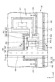
- FIG. 1 is a plan view of a liquid crystal panel constituting a liquid crystal display device according to Embodiment 1 of the present invention.
- Sectional drawing which shows schematically the structure in the display area of a liquid crystal panel
- the top view which shows roughly the structure in the display area of CF board
- the top view which shows roughly the structure in the display area of the array board
- Cross-sectional view around the TFT (corresponding to the view cut along line VI-VI in FIG. 5)
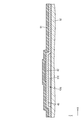
- Sectional drawing which shows conductive film formation process Sectional drawing which shows the 1st resist formation process
- Sectional drawing which shows the 1st etching process Sectional view of the vicinity of the semiconductor film after completion of the first etching step (corresponding to a view taken along line VII-VII in FIG. 5)
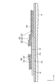
- Sectional drawing which shows 2nd resist formation process Sectional view showing the second etching step
- Sectional drawing of the semiconductor film vicinity in the state which the 2nd etching process was completed The top view which shows the resist which concerns on Embodiment 2 of this invention
- FIGS. 1 A first embodiment of the present invention will be described with reference to FIGS.
- the liquid crystal panel 11 display panel included in the liquid crystal display device is illustrated.
- Each drawing shows the X-axis, Y-axis, and Z-axis, and each axis is drawn so as to be the direction shown in each drawing.
- the upper side of FIG.2, FIG6, FIG.7 etc. be a front side, and let the lower side of the figure be a back side.
- the liquid crystal display device includes the liquid crystal panel 11 shown in FIG. 1 and a backlight device (illumination device, not shown) that is an external light source that irradiates the liquid crystal panel 11 with light for display.
- the liquid crystal panel 11 will be described in detail with respect to the components of the liquid crystal display device, but other components such as the backlight device are well known and will not be described in detail.
- the liquid crystal panel 11 has a vertically long rectangular shape (rectangular shape) as a whole, and an image is displayed at a position offset to one side (the upper side in FIG. 1) in the long side direction.
- a display area A1 active area
- a driver 12 and a flexible substrate 13 for supplying various signals and the like are respectively attached to positions on the other side (lower side in FIG. 1) in the long side direction.
- An area outside the display area A1 in the liquid crystal panel 11 is a non-display area A2 (non-active area) where no image is displayed.
- This non-display area A2 is a substantially frame-shaped area (a CF substrate described later) surrounding the display area A1.
- the area secured on the other end side in the side direction includes a mounting area (attachment area) for the driver 12 and the flexible substrate 13.
- a control board 14 that is a signal supply source is connected to the end of the flexible board 13 opposite to the liquid crystal panel 11 side.
- a frame-shaped dot-and-dash line represents the outer shape of the display area A1, and a region outside the dot-and-dash line is a non-display area A2.
- the driver 12 is composed of an LSI chip having a drive circuit therein, and operates based on a signal supplied from the control board 14 to generate an output signal.
- the output signal is displayed on the display area of the liquid crystal panel 11. Output to A1.
- the driver 12 has a horizontally long rectangular shape when viewed in a plan view (longitudinal along the short side of the liquid crystal panel 11) and is directly mounted on the non-display area A2 of the liquid crystal panel 11 (array substrate 30). That is, COG (Chip On Glass) is mounted.
- the flexible substrate 13 includes a base material made of a synthetic resin material having insulation properties and flexibility (for example, polyimide resin), and has a large number of wiring patterns (not shown) on the base material.
- the one end side in the length direction is connected to the control substrate 14, while the other end side is connected to the liquid crystal panel 11 (array substrate 30).
- the flexible substrate 13 is bent in a folded shape so that the cross-sectional shape is substantially U-shaped in the liquid crystal display device.
- the wiring pattern is exposed to the outside to form terminal portions (not shown), and these terminal portions are respectively connected to the control substrate 14 and the liquid crystal panel 11. Are electrically connected. As a result, a signal supplied from the control board 14 side can be transmitted to the liquid crystal panel 11 side.
- the control board 14 is disposed on the back side of the backlight device.
- electronic parts for supplying various signals to the driver 12 are mounted on a board made of paper phenol or glass epoxy resin, and a predetermined pattern wiring (conductive path) is routed and formed.
- a predetermined pattern wiring conductive path
- One end of the flexible substrate 13 is electrically and mechanically connected to the control substrate 14 via an ACF (Anisotropic Conductive Film) (not shown).
- the liquid crystal panel 11 includes a pair of substrates 20 and 30 and liquid crystal molecules that are disposed in an internal space between the substrates 20 and 30 and are substances whose optical characteristics change with application of an electric field. And a liquid crystal layer 16 (medium layer).
- the liquid crystal layer 16 is sealed by being surrounded by a seal portion (not shown) interposed between both the substrates 20 and 30.
- the front side (front side) of the pair of substrates 20 and 30 is the CF substrate 20 (counter substrate, color filter substrate), and the back side (back side) is the array substrate 30 (display substrate, active matrix substrate, element substrate).
- the Polarizing plates 17A and 17B are attached to the outer surface sides of both substrates 20 and 30, respectively.
- alignment layers 18A and 18B for aligning liquid crystal molecules contained in the liquid crystal layer 16 are formed as the innermost layers of the substrates 20 and 30 and in contact with the liquid crystal layer 16, respectively.
- the CF substrate 20 is formed by laminating various films on the inner surface side of a glass substrate 21 made of glass.
- a color filter 22 is provided at a position facing a pixel electrode 31 (described later) on the array substrate 30 side. Yes.
- the color filter 22 is formed by repeatedly arranging three colored portions of R (red), G (green), and B (blue) in a matrix.
- the colored portions (pixels 19) of the color filter 22 arranged in a matrix are partitioned by a light shielding portion 23 (black matrix).
- the light shielding portion 23 prevents the light of each color that passes through each colored portion from being mixed (color mixing).
- an overcoat film 24 (flattening film) is provided on the inner surface of the color filter 22 and the light shielding portion 23 so as to overlap each other.
- one pixel 19 is configured by a set of the colored portion in the color filter 22 and the pixel electrode 31 facing the colored portion. More specifically, the liquid crystal panel 11 includes a pixel 19 (red pixel) having a red colored portion of the color filter 22, a pixel 19 (green pixel) having a green colored portion of the color filter 22, and a color.
- the filter 19 includes a pixel 19 (blue pixel) having a blue coloring portion.
- the three color pixels 19 are arranged repeatedly in the row direction (X-axis direction) on the plate surface of the liquid crystal panel 11 to form a pixel group, and this pixel group is arranged in the column direction (Y-axis direction). ) Are arranged side by side along. That is, a large number of pixels 19 are arranged in a matrix in the display area A1 of the liquid crystal panel 11.
- the array substrate 30 is formed by laminating various films on the inner surface side of a glass substrate 32 made of glass by a photolithography method.
- TFTs 34 Thin Film Transistor: display elements
- pixels that are switching elements A large number of electrodes 31 (two-dot chain lines in FIG. 4) are arranged in a matrix (matrix), and around the TFT 34 and the pixel electrode 31 are a gate wiring 35G (scanning line) and a source wiring 36S (data). Lines, signal lines, and element wiring portions) are arranged in a lattice shape.
- the TFT 34 includes a gate electrode 37G, a source electrode 38S, and a drain electrode 39D, as shown in FIGS.
- the gate wiring 35G is connected to the gate electrode 37G
- the source wiring 36S is connected to the source electrode 38S.
- one end of a drain wiring 40D is connected to the drain electrode 39D.
- an element connection portion 41D connected to the pixel electrode 31 is formed integrally with the drain wiring 40D.
- the TFT 34 has a channel portion 42A that connects the drain electrode 39D and the source electrode 38S.
- the TFT 34 is driven based on various signals respectively supplied to the gate wiring 35G and the source wiring 36S, and the potential supply to the pixel electrode 31 is controlled in accordance with the driving.
- the extending direction of the gate line 35G coincides with the X-axis direction
- the extending direction of the source line 36S coincides with the Y-axis direction.
- the pixel electrode 31 is arranged in a rectangular region surrounded by the gate wiring 35G and the source wiring 36S, and a plurality of slits (not shown) are formed.
- a common electrode 33 is provided on the back side of the pixel electrode 31 as shown in FIG. 2.
- the liquid crystal layer 16 has a fringe electric field including a component in the normal direction to the plate surface of the array substrate 30 in addition to a component along the plate surface of the array substrate 30. (Oblique electric field) is applied. That is, the operation mode of the liquid crystal panel 11 is FFS (Fringe Field Switching) mode.
- the glass substrate 32 includes a gate conductive film 43G, a gate insulating film 45, a semiconductor film 42, and a source conductive film 46S (and from the lower layer side (side closer to the glass substrate 32)).
- the drain conductive film 46D), the first interlayer insulating film 47, the planarizing film 48, the common electrode 33 (transparent electrode film), the second interlayer insulating film 49, and the pixel electrode 31 (transparent electrode film) are laminated.
- the illustration of the alignment film 18A laminated on the upper layer side of the pixel electrode 31 is omitted.
- the gate conductive film 43G constitutes the gate electrode 37G and the gate wiring 35G.
- the gate conductive film 43G is formed of, for example, a laminated film of three layers of titanium (Ti) layer / aluminum (Al) layer / titanium layer.
- the gate insulating film 45 is made of, for example, silicon oxide (SiO 2 ) that is an inorganic material. The gate insulating film 45 is interposed between the gate conductive film 43G and the source conductive film 46S (or the drain conductive film 46D), and insulates each other.
- the semiconductor film 42 is formed on the gate insulating film 45 at a location overlapping the gate electrode 37G, and is made of a thin film using an oxide semiconductor as a material.
- the semiconductor film 42 mainly constitutes the channel portion 42A of the TFT 34.
- no etch stop layer is formed on the channel portion 42A, and the lower surfaces of the source electrode 38S and the drain electrode 39D are directly connected to the upper surface of the semiconductor film 42, respectively.
- the oxide semiconductor included in the semiconductor film 42 may be an amorphous oxide semiconductor or a crystalline oxide semiconductor having a crystalline portion.
- the crystalline oxide semiconductor include a polycrystalline oxide semiconductor, a microcrystalline oxide semiconductor, and a crystalline oxide semiconductor in which the c-axis is oriented substantially perpendicular to the layer surface.
- the semiconductor film 42 may have a stacked structure of two or more layers. In the case where the semiconductor film 42 has a stacked structure, the semiconductor film 42 may include an amorphous oxide semiconductor layer and a crystalline oxide semiconductor layer. Alternatively, a plurality of crystalline oxide semiconductor layers having different crystal structures may be included. In addition, a plurality of amorphous oxide semiconductor layers may be included.
- the energy gap of the oxide semiconductor included in the upper layer is preferably larger than the energy gap of the oxide semiconductor included in the lower layer.
- the energy gap of the lower oxide semiconductor may be larger than the energy gap of the upper oxide semiconductor.
- the semiconductor film 42 may include at least one metal element of In, Ga, and Zn.
- the semiconductor film 42 includes, for example, an In—Ga—Zn—O-based semiconductor (eg, indium gallium zinc oxide).
- Such a semiconductor film 42 can be formed of an oxide semiconductor film containing an In—Ga—Zn—O-based semiconductor.
- the In—Ga—Zn—O-based semiconductor may be either amorphous or crystalline.
- a crystalline In—Ga—Zn—O-based semiconductor a crystalline In—Ga—Zn—O-based semiconductor in which the c-axis is oriented substantially perpendicular to the layer surface is preferable.
- a TFT having an In—Ga—Zn—O-based semiconductor layer has high mobility (more than 20 times that of an a-Si TFT) and low leakage current (less than one hundredth of that of an a-Si TFT).
- the TFT is suitably used as a driving TFT (not shown) (for example, a TFT included in a driving circuit provided on the same substrate as the display area around the display area including a plurality of pixels) and a TFT (TFT provided in the pixel).
- a driving TFT for example, a TFT included in a driving circuit provided on the same substrate as the display area around the display area including a plurality of pixels
- TFT provided in the pixel
- the semiconductor film 42 may contain another oxide semiconductor instead of the In—Ga—Zn—O-based semiconductor.
- an In—Sn—Zn—O-based semiconductor eg, In 2 O 3 —SnO 2 —ZnO; InSnZnO
- the In—Sn—Zn—O-based semiconductor is a ternary oxide of In (indium), Sn (tin), and Zn (zinc).
- the semiconductor film 42 includes an In—Al—Zn—O based semiconductor, an In—Al—Sn—Zn—O based semiconductor, a Zn—O based semiconductor, an In—Zn—O based semiconductor, and a Zn—Ti—O based semiconductor.
- the source conductive film 46S and the drain conductive film 46D are formed on the gate insulating film 45.
- the source conductive film 46S constitutes the source wiring 36S and the source electrode 38S.
- the drain conductive film 46D constitutes the drain electrode 39D, the drain wiring 40D, and the element connection portion 41D.
- the source conductive film 46S and the drain conductive film 46D are formed of the same material, and are formed of, for example, a laminated film of three layers of titanium layer / aluminum layer / titanium layer.
- the first interlayer insulating film 47 is disposed on at least the source conductive film 46S (and the drain conductive film 46D), and is made of, for example, silicon oxide (SiO 2 ) that is an inorganic material.
- the planarizing film 48 is disposed on the first interlayer insulating film 47 and is made of, for example, an acrylic resin material (for example, polymethyl methacrylate resin (PMMA)) that is an organic resin material.
- PMMA polymethyl methacrylate resin
- planarizing film 48 is an organic insulating film, and its thickness is made thicker than other inorganic insulating films (the first interlayer insulating film 47 and the second interlayer insulating film 49), and the surface is planarized. It has a function.
- the common electrode 33 is disposed on the planarizing film 48 and is made of a transparent electrode material such as ITO (Indium Tin Oxide) or ZnO (Zinc Oxide).
- the second interlayer insulating film 49 is disposed on at least the common electrode 33 and is made of, for example, silicon nitride (SiNx) that is an inorganic material.
- the second interlayer insulating film 49 is interposed between the common electrode 33 and the pixel electrode 31 to insulate each other.
- the pixel electrode 31 is disposed on the second interlayer insulating film 49 and is made of a transparent electrode material such as ITO (Indium Tin Oxide) or ZnO (Zinc Oxide).
- a contact hole CH1 (see the broken line in FIG. 6) is formed at a portion overlapping with the element connection portion 41D, and the pixel electrode 31 passes through the contact hole CH1.
- stacked on the glass substrate 32 is not limited to what was mentioned above, It can change suitably.
- liquid crystal panel manufacturing method Next, a method for manufacturing the liquid crystal panel 11 will be described.
- the liquid crystal panel 11 according to the present embodiment is manufactured by bonding the CF substrate 20 and the array substrate 30 after manufacturing the CF substrate 20 and the array substrate 30 respectively.
- a method for manufacturing the array substrate 30 constituting the liquid crystal panel 11 will be described in detail.
- the manufacturing method of the array substrate 30 includes a gate conductive film forming step for forming the gate conductive film 43G, a gate insulating film forming step for forming the gate insulating film 45, a semiconductor film forming step for forming the semiconductor film 42, A source / drain formation process for forming the source conductive film 46S and the drain conductive film 46D, a first interlayer insulation film formation process for forming the first interlayer insulation film 47, and a planarization film formation process for forming the planarization film 48 And a common electrode forming step for forming the common electrode 33, a second interlayer insulating film forming step for forming the second interlayer insulating film 49, and a pixel electrode forming step for forming the pixel electrode 31.
- each of the above-described processes includes a film forming process for forming a thin film that is a base of the thin film pattern, and a resist pattern having a shape corresponding to the thin film pattern by performing exposure processing and development processing on the resist. And a resist forming process for forming a thin film pattern by performing etching using the resist pattern as a mask.
- a plasma CVD method, a sputtering method, a vacuum evaporation method, or the like is appropriately used depending on the type of the thin film.
- the etching process wet etching or dry etching is appropriately used depending on the type of thin film to be etched.
- the source / drain formation process of this embodiment differs from the other thin film formation processes in that the resist formation process and the etching process are performed twice.
- the source / drain formation process will be described in detail.
- Source drain formation process In the source / drain formation process, a conductive film formation process for forming the conductive film 51 to be the basis of the source conductive film 46S and the drain conductive film 46D, and a resist 52R following the shapes of the source conductive film 46S and the drain conductive film 46D.
- a first resist forming step for forming a source a first etching step for forming the source conductive film 46S and the drain conductive film 46D by etching the conductive film 51 using the resist 52R as a mask, the semiconductor film 42, and the source
- a conductive film 51 is formed (film formation) so as to cover both the gate insulating film 45 and the semiconductor film 42.
- the conductive film 51 is formed in a solid form over the entire display area A1 of the array substrate 30.
- a resist photoresist
- a patterned resist 52R resist pattern
- the formation range of the resist 52R is substantially the same as the formation range of the source conductive film 46S and the drain conductive film 46D.
- the conductive film 51 is etched using the resist 52R as a mask.
- the portion of the conductive film 51 covered with the resist 52R remains without being etched, but the portion not covered with the resist 52R is removed (see FIGS. 9 and 10). That is, the planar shape of the resist 52R is transferred to the etched conductive film 51, and the source conductive film 46S and the drain conductive film 46D are formed.
- the resist 52R is stripped through a resist stripping step after finishing the first etching step.
- the type of etching performed here is not particularly limited as long as the conductive film 51 can be removed. For example, dry etching is performed.
- the type of etching can be appropriately changed according to the type of the conductive film 51 and the required dimensional accuracy, and wet etching may be performed.
- dry etching and wet etching may be selectively used depending on the type of each thin film.
- the gate insulating film 45 is disposed so as to cover the gate conductive film 43G.
- the gate insulating film 45 has a step 45A due to the thickness of the gate conductive film 43G.
- the resist 52R since the thickness of the resist 52R is likely to be larger than other portions, when the resist 52R is patterned, the resist 52R that would otherwise be removed tends to remain. . If the resist 52R remains, the conductive film 51 is not removed by etching at that portion, and as a result, there is a concern that a residue 51A of the conductive film 51 is generated in the stepped portion 45A.
- the stepped portion 45A has a tapered shape having an inclined surface that is inclined with respect to the plate surface of the glass substrate 32, and the residue 51A becomes more as the inclined angle of the inclined surface is larger. It is likely to occur.
- the stepped portion 45A is a portion corresponding to the peripheral end portion of the gate conductive film 43G, specifically, a portion overlapping the peripheral end portion of the gate conductive film 43G in plan view (or a portion slightly outside the peripheral end portion). ).
- a portion (step 45 ⁇ / b> A) where the residue 51 ⁇ / b> A may be generated is indicated by dark shading.
- the residue 51A is generated, there is a concern that the adjacent source conductive film 46S and drain conductive film 46D are connected by the residue 51A.
- a plurality of pairs of source conductive films 46S and drain conductive films 46D are formed so as to be arranged along the extending direction of the gate wiring 35G (X-axis direction in FIG. 4). Therefore, as shown in FIG. 4, there is a concern that the two adjacent source conductive films 46S are connected by the residue 51A.
- the second resist forming step and the second etching step are performed after the first etching step for the purpose of removing the residue 51A of the conductive film 51 while protecting the semiconductor film 42.
- a resist (photoresist) is applied to the upper layer side of the semiconductor film 42, the source conductive film 46S, and the drain conductive film 46D, and the resist is applied to a predetermined photomask. Then, after the exposed resist is developed, a patterned resist 53R (resist pattern) is formed as shown in FIGS. As shown in FIG. 5, the resist 53R covers the semiconductor film 42, the source conductive film 46S, and the drain conductive film 46D. In the plan view of FIG. 5, the patterned resist 53R is indicated by thin shading, and the peripheral edge of the resist 53R is indicated by a two-dot chain line.
- the resist 53R follows the shape of the semiconductor film 42, the source conductive film 46S, and the drain conductive film 46D in the plan view shown in FIG.
- the resist 53R has a shape that is slightly larger than the source conductive film 46S and the drain conductive film 46D in plan view.
- the distance L1 from the peripheral edge of the source conductive film 46S (or the drain conductive film 46D) to the peripheral edge of the resist 53R is set to 1 ⁇ m, for example, but is not limited to this value and can be changed as appropriate.
- the resist 53R is provided in such a way as to avoid a portion where a short circuit may occur due to the generation of the residue 51A in the stepped portion 45A extending along the peripheral edge of the gate conductive film 43G.
- the resist 53R is formed so as to avoid the three extending portions 45B, 45D, and 45E in the stepped portion 45A.
- the extending portion 45B has a portion (L-shaped portion) extending over both the source conductive film 46S and the drain conductive film 46D connected through the semiconductor film 42 in the stepped portion 45A. Part).
- the extending portion 45D is a portion extending over both of the two adjacent source conductive films 46S in the stepped portion 45A.
- the extending portion 45E (opposite side extending portion) includes the drain conductive film 46D and the drain conductive film 46D (for example, reference numeral 46D1 in FIG. 4) of the stepped portion 45A through the semiconductor film 42. This is a part extending over both of the source conductive films 46S (for example, reference numeral 46S1 in FIG. 4) on the side not connected.
- the source conductive film 46S1 corresponds to the drain conductive film 46D out of the two source conductive films 46S arranged with the drain conductive film 46D interposed therebetween.
- the resist 53R may be arranged so as to avoid at least a part of the extending portion 45B in the extending direction. In other words, it suffices that a part of the peripheral end portion of the resist 53R is arranged so as to intersect the extending portion 45B.
- the residue 51A can be cut in the second etching step described later.
- the extending portions 45D and 45E may be arranged such that the resist 53R avoids at least a part of the extending portions 45D and 45E in the extending direction.
- etching that can remove the conductive film 51 is performed using the resist 53R as a mask.
- the same type of etching as that performed in the first etching step is performed, but the present invention is not limited to this.
- the residue 51A of the stepped portion 45A is removed.
- the resist 53R is stripped through a resist stripping step after finishing the first etching step.
- etching is performed until a part 45F (indicated by a two-dot chain line in FIG. 13) of the gate insulating film 45 is removed, so that the residue 51A of the conductive film 51 is more reliably removed. can do.
- a conductive film forming step for forming the conductive film 51 so as to cover both the films 42 and a source electrode 38S connected to the semiconductor film 42 by etching the conductive film 51 are performed after the conductive film forming step.
- the first etching process for forming the source conductive film 46S and the drain conductive film 46D having the drain electrode 39D connected to the semiconductor film 42, and the semiconductor film 42, the source conductive film are performed after the first etching process.
- the resist 53R as a mask comprises a second etching step for removable etch the conductive film 51.
- a stepped portion 45 ⁇ / b> A is generated at a location overlapping the peripheral end portion of the gate electrode 37 ⁇ / b> G and a location overlapping the peripheral end portion of the gate wiring 35 ⁇ / b> G due to the thickness of the gate electrode 37 ⁇ / b> G and the gate wiring 35 ⁇ / b> G.
- the source conductive film 46S and the drain conductive film 46D are formed on the gate insulating film 45 by etching, the conductive film 51 is hardly removed at the stepped portion 45A of the gate insulating film 45, and the residue 51A of the conductive film 51 is removed. There is concern about the situation that will occur.
- a resist 53R is formed to cover the semiconductor film 42, the source conductive film 46S, and the drain conductive film 46D.
- Etching capable of removing the conductive film 51 is performed (second etching step). For this reason, even if the conductive film 51 remains in the step portion 45A of the gate insulating film 45, it can be removed.
- the semiconductor film 42 is covered with the resist 53R, the semiconductor film 42 can be protected from etching.
- the resist 45 avoids at least a part of the extending portion 45B extending over both the source conductive film 46S and the drain conductive film 46D among the stepped portions 45A formed in the gate insulating film 45. 53R is formed.
- the resist 53R is formed avoiding at least a part of the extended portion 45B. Thereby, even if the residue 51A connecting the conductive film 46S for the source and the conductive film 46D for the drain is generated in the extended portion 45B, the residue 51A can be removed (cut) in the second etching step. A situation in which the source electrode 38S and the drain electrode 39D are electrically connected through the residue 51A can be suppressed.
- a plurality of source conductive films 46S and drain conductive films 46D are formed along the extending direction of the gate wiring 35G, and in the resist forming process, they are formed on the gate insulating film 45.
- the resist 53R can be formed avoiding at least a part of the extended portion 45D extending over both of the two adjacent source conductive films 46S.
- the residue 51A of the conductive film 51 generated between the two adjacent source conductive films 46S in the second etching step can be removed, and the two adjacent source conductive films 46S pass through the residue 51A of the conductive film 51.
- the situation where it is electrically connected can be suppressed.
- a plurality of source conductive films 46S and drain conductive films 46D are formed along the extending direction of the gate wiring 35G, and the drain conductive film 46D is interposed therebetween.
- the source conductive film 46S disposed on the opposite side of the source conductive film 46S connected to the drain conductive film 46D via the semiconductor film 42 is used as the source conductive film.
- the film 46S1 in the resist formation step at least one of the extended portions 45E extending over both the drain conductive film 46D and the source conductive film 46S1 among the stepped portions 45A formed in the gate insulating film 45.
- the resist 53R is formed avoiding the portion.
- the residue 51A connecting the drain conductive film 46D and the source conductive film 46S1 can be removed in the second etching step, and the drain conductive film 46D and the source conductive film 46S1. Can be prevented from being electrically connected through the residue 51A of the conductive film 51.
- a resist 53R having a shape that follows the shape of the source conductive film 46S and the drain conductive film 46D is formed.
- the source conductive film 46S and the drain conductive film 46D can be removed at substantially the same locations as those removed in the first etching step.
- overetching is generally performed in order to reliably remove unnecessary conductive films.
- the etching time in the first etching step (more specifically, the time for performing overetching) can be reduced, and etching for the reduced time can be performed in the second etching step.
- the gate electrode 37G and the gate wiring 35G include aluminum.
- aluminum has a higher electrical resistance than copper. Therefore, when aluminum is used for the gate electrode 37G and the gate wiring 35G, it is preferable to make the gate electrode 37G and the gate wiring 35G thicker than when copper is used in order to reduce electrical resistance.
- the gate electrode 37G and the gate wiring 35G are thickened, the height of the stepped portion 45A of the gate insulating film 45 resulting from the thickness of the gate electrode 37G and the gate wiring 35G also increases, so that the residue 51A of the conductive film 51 is more likely to occur. Become. In the present embodiment, since the residue 51A of the conductive film 51 can be removed in the second etching step, it is particularly suitable when aluminum is used for the gate electrode 37G and the gate wiring 35G.
- Embodiment 2 of the present invention will be described with reference to FIG.
- the formation range of the resist formed in the second resist forming step is different from that of the above embodiment. Note that the same portions as those in the above embodiment are denoted by the same reference numerals and redundant description is omitted.
- the resist 153R resist pattern, thin shaded portion in FIG. 15
- the second resist forming step of the present embodiment is formed over the entire display area A1 in the array substrate 30. And has two types of openings 154 and 155. For example, one opening 154, 155 is provided for each pixel 19, but the present invention is not limited to this.
- the opening 154 has a rectangular shape in a plan view and is arranged so as to intersect with the extending portion 45B in the stepped portion 45A.
- the opening 154 is formed in order to remove the residue 51A of the conductive film 51 generated in the extending portion 45B.
- the opening 155 has a rectangular shape in a plan view and is arranged so as to intersect with both the extending portions 45D and 45E in the stepped portion 45A.
- the opening 155 is formed in order to remove the residue 51A of the conductive film 51 generated in the extending portions 45D and 45E.
- the shape of the openings 154 and 155 is not limited to a rectangle and can be changed as appropriate.
- the resist 153R is configured to cover portions other than the openings 154 and 155 in the display area A1.
- the resist 153R covers the gate insulating film 45, the source conductive film 46S, the gate conductive film 43G, the drain conductive film 46D, and the semiconductor film 42, and may cause a short circuit between the conductive films due to the residue 51A.
- the structure is not covered.
- By performing the second etching step using such a resist 153R as a mask a part of the residue 51A generated in each of the extending portions 45B, 45D, 45E can be removed. That is, the residue 51A extending between the conductive films can be cut. Since the gate insulating film 45 is covered with the resist 153R, the situation where it is removed in the second etching step can be suppressed.
- the present invention is not limited to the embodiments described with reference to the above description and drawings.
- the following embodiments are also included in the technical scope of the present invention.
- (1) the liquid crystal panel whose planar shape is rectangular has been exemplified.
- the present invention can also be applied to a liquid crystal panel whose planar shape is square, circular, elliptical, or the like.
- (2) In each of the above-described embodiments, the case where the driver is COG-mounted on the array substrate of the liquid crystal panel is shown. However, the driver is configured to be mounted on the flexible substrate by COF (Chip On Film). Also good.
- COF Chip On Film
- the semiconductor film constituting the channel portion of the TFT is made of an oxide semiconductor material
- polysilicon polycrystallized silicon (polycrystal It is also possible to use CG silicon (Continuous Grain Silicon)) which is a kind of silicon) or amorphous silicon as a material for the semiconductor film.
- CG silicon Continuous Grain Silicon
- amorphous silicon a material for the semiconductor film.
- the liquid crystal panel in which the operation mode is set to the FFS mode is illustrated, but other than that, there are other modes such as an IPS (In-Plane Switching) mode and a VA (Vertical Alignment) mode
- the present invention can also be applied to a liquid crystal panel in the operation mode.
- the color filter of the liquid crystal panel is exemplified as a three-color configuration of red, green and blue.
- a yellow colored portion is added to each colored portion of red, green and blue.
- the present invention can also be applied to a color filter having a four-color configuration.
- the material of the conductive film 51 is not limited to that described above, and can be changed as appropriate.
- a metal film such as chromium (Cr), tantalum (Ta), or copper (Cu) can be used in addition to aluminum and titanium, and these metal films may be stacked.
- the configuration in which the resist 53R formed in the second resist forming step is slightly larger than the source conductive film 46S and the drain conductive film 46D in plan view is illustrated.
- the resist 53R may have a shape that completely matches the shapes of the source conductive film 46S and the drain conductive film 46D in plan view.
- the shapes (formation ranges) of the gate conductive film 43G, the source conductive film 46S, and the drain conductive film 46D are not limited to those illustrated in the above embodiment, and can be changed as appropriate.
Abstract
The manufacturing method for a substrate for a display panel is characterized by comprising a conductive film formation step for forming a conductive film so as to cover both a gate insulation film 45A, etc. formed on a glass substrate and covering a gate electrode 37G and a gate wire 35G, and a semiconductor film 42 formed on a location overlapping the gate electrode 37G on the gate insulation film 45A, etc.; a first etching step for forming, by etching conductive films, a conductive film 46S for a source connected to the semiconductor film 42 and a conductive film 46D for a drain connected to the semiconductor film 42; a resist formation step for forming a resist 53R covering the semiconductor film 42, the conductive film 46S for a source, and the conductive film 46D for a drain, performed after the first etching step; and a second etching step for removably etching a conductive film 51A using the resist 53R as a mask, performed after the resist formation step.
Description
本発明は、表示パネル用基板の製造方法に関する。
The present invention relates to a method for manufacturing a display panel substrate.
従来、液晶表示装置に用いられる表示基板の一例として下記特許文献1に記載されたものが知られている。特許文献1に記載された表示基板は、透明基板上にゲート配線、ゲート絶縁膜、半導体膜、ソース配線(及びドレイン配線)の順番で積層されている。
Conventionally, what was described in the following patent document 1 is known as an example of the display substrate used for a liquid crystal display device. The display substrate described in Patent Document 1 is laminated on a transparent substrate in the order of gate wiring, gate insulating film, semiconductor film, and source wiring (and drain wiring).
(発明が解決しようとする課題)
上記構成においては、ゲート配線の上層にゲート絶縁膜を配することから、ゲート配線の厚さの分だけ、ゲート絶縁膜に段差部が生じる。このような段差部では、ソース配線及びドレイン配線をエッチングによって形成する際の導電膜の残渣が生じ易く、短絡の原因となる。特に近年では、解像度の高い表示装置を実現するために、配線の幅を小さくしつつ、低抵抗化することが求められている。このため、低抵抗化するために、ゲート配線の厚さが大きくなる傾向にあり、段差部の高さも大きくなることから、エッチング時の導電膜の残渣がより残り易いという問題点がある。 (Problems to be solved by the invention)
In the above configuration, since the gate insulating film is disposed on the upper layer of the gate wiring, a stepped portion is generated in the gate insulating film by the thickness of the gate wiring. In such a step portion, a residue of the conductive film is easily generated when the source wiring and the drain wiring are formed by etching, which causes a short circuit. Particularly in recent years, in order to realize a display device with high resolution, it is required to reduce the resistance while reducing the width of the wiring. For this reason, in order to reduce the resistance, the thickness of the gate wiring tends to increase, and the height of the stepped portion also increases. Therefore, there is a problem that the conductive film residue during etching tends to remain.
本発明は上記のような事情に基づいて完成されたものであって、導電膜の残渣を除去することを目的とする。
The present invention has been completed based on the above situation, and an object thereof is to remove the residue of the conductive film.
(課題を解決するための手段)
上記課題を解決するために、本発明の表示パネル用基板の製造方法は、基板上に形成されたゲート電極及びゲート配線を覆うゲート絶縁膜、及び前記ゲート絶縁膜上において前記ゲート電極と重なる箇所に形成された半導体膜の双方を覆う形で導電膜を形成する導電膜形成工程と、前記導電膜形成工程の後に行われ、前記導電膜をエッチングすることで、前記半導体膜と接続されるソース電極を有するソース用導電膜、及び前記半導体膜と接続されるドレイン電極を有するドレイン用導電膜を形成する第1エッチング工程と、前記第1エッチング工程の後に行われ、前記半導体膜、前記ソース用導電膜、前記ドレイン用導電膜を覆うレジストを形成するレジスト形成工程と、前記レジスト形成工程の後に行われ、前記レジストをマスクとして、前記導電膜を除去可能なエッチングを行う第2エッチング工程と、を備えることに特徴を有する。 (Means for solving the problem)
In order to solve the above problems, a method for manufacturing a substrate for a display panel according to the present invention includes a gate electrode formed on the substrate and a gate insulating film covering the gate wiring, and a portion overlapping the gate electrode on the gate insulating film. A conductive film forming step of forming a conductive film so as to cover both of the semiconductor films formed on the substrate, and a source connected to the semiconductor film by etching the conductive film after the conductive film formation step A first etching step of forming a source conductive film having an electrode and a drain conductive film having a drain electrode connected to the semiconductor film; and after the first etching step, the semiconductor film, the source A resist forming step of forming a conductive film and a resist covering the drain conductive film; and after the resist forming step, using the resist as a mask Characterized in that and a second etching step for removable etching the conductive film.
ゲート絶縁膜においてゲート電極の周端部と重なる箇所、及びゲート配線の周端部と重なる箇所には、ゲート電極及びゲート配線の厚みに起因して段差部が生じる。ゲート絶縁膜上にソース用導電膜及びドレイン用導電膜をエッチングによって形成する場合には、ゲート絶縁膜の段差部では、導電膜が除去され難く、導電膜の残渣が生じる事態が懸念される。上記構成においては、第1エッチング工程において、ソース用導電膜及びドレイン用導電膜を形成した後、半導体膜、ソース用導電膜及びドレイン用導電膜を覆うレジストを形成し、導電膜を除去可能なエッチングを行う(第2エッチング工程)。このため、ゲート絶縁膜の段差部に導電膜が残っていた場合であっても、これを除去することができる。また、第2エッチング工程では、半導体膜がレジストによって覆われているから、半導体膜をエッチングから保護することができる。
In the gate insulating film, a stepped portion is generated at a portion overlapping with the peripheral end portion of the gate electrode and a portion overlapping with the peripheral end portion of the gate wiring due to the thickness of the gate electrode and the gate wiring. When the source conductive film and the drain conductive film are formed on the gate insulating film by etching, the conductive film is difficult to remove at the stepped portion of the gate insulating film, and there is a concern that a conductive film residue may be generated. In the above structure, after the source conductive film and the drain conductive film are formed in the first etching step, a resist covering the semiconductor film, the source conductive film, and the drain conductive film is formed, and the conductive film can be removed. Etching is performed (second etching step). For this reason, even if the conductive film remains in the step portion of the gate insulating film, it can be removed. In the second etching step, since the semiconductor film is covered with the resist, the semiconductor film can be protected from etching.
上記構成において、前記レジスト形成工程では、前記ゲート絶縁膜に形成された段差部のうち、前記ソース用導電膜と前記ドレイン用導電膜の双方に亘って延びる延設部の少なくとも一部を避けて前記レジストを形成するものとすることができる。
In the above configuration, in the resist forming step, avoiding at least a part of the extending portion extending over both the source conductive film and the drain conductive film among the stepped portions formed in the gate insulating film. The resist may be formed.
ゲート絶縁膜に形成された段差部のうちソース用導電膜からドレイン用導電膜に亘って延びる延設部に導電膜の残渣が生じると、導電膜の残渣を介してソース電極及びドレイン電極が電気的に接続される事態が懸念される。本発明では、延設部の少なくとも一部を避けてレジストを形成する。これにより、段差部の一部である延設部にソース用導電膜及びドレイン用導電膜を繋ぐ残渣が生じた場合であっても、その残渣を第2エッチング工程において除去することができ、導電膜の残渣を介してソース電極及びドレイン電極が電気的に接続される事態を抑制することができる。
When a conductive film residue is generated in an extended portion extending from the source conductive film to the drain conductive film in the stepped portion formed in the gate insulating film, the source electrode and the drain electrode are electrically connected through the conductive film residue. There is concern about the situation of being connected. In the present invention, the resist is formed avoiding at least a part of the extended portion. Thus, even when a residue connecting the source conductive film and the drain conductive film is formed in the extended portion which is a part of the stepped portion, the residue can be removed in the second etching step. A situation in which the source electrode and the drain electrode are electrically connected through the residue of the film can be suppressed.
また、前記第1エッチング工程では、前記ソース用導電膜及び前記ドレイン用導電膜を、前記ゲート配線の延設方向に沿って複数配列する形で形成し、前記レジスト形成工程では、前記ゲート絶縁膜に形成された段差部のうち、隣り合う2つの前記ソース用導電膜の双方に亘って延びるソース間延設部の少なくとも一部を避けて前記レジストを形成するものとすることができる。
In the first etching step, a plurality of the conductive film for source and the conductive film for drain are formed along the extending direction of the gate wiring, and the gate insulating film is formed in the resist forming step. The resist can be formed by avoiding at least a part of the inter-source extending portion that extends over both of the two adjacent source conductive films among the step portions formed in step (b).
第2エッチング工程において隣り合う2つのソース用導電膜間に生じる導電膜の残渣を除去することができ、隣り合う2つのソース用導電膜同士が導電膜の残渣を介して電気的に接続される事態を抑制することができる。
The residue of the conductive film generated between two adjacent source conductive films in the second etching step can be removed, and the two adjacent source conductive films are electrically connected to each other through the conductive film residue. The situation can be suppressed.
また、前記第1エッチング工程では、前記ソース用導電膜及び前記ドレイン用導電膜を、前記ゲート配線の延設方向に沿って複数配列する形で形成し、前記ドレイン用導電膜を挟む形で配される2つの前記ソース用導電膜のうち、前記ドレイン用導電膜に対して前記半導体膜を介して接続される前記ソース用導電膜とは反対側に配される前記ソース用導電膜を反対側ソース用導電膜とした場合において、前記レジスト形成工程では、前記ゲート絶縁膜に形成された段差部のうち、前記ドレイン用導電膜と前記反対側ソース用導電膜の双方に亘って延びる反対側延設部の少なくとも一部を避けて前記レジストを形成するものとすることができる。
In the first etching step, a plurality of the source conductive film and the drain conductive film are formed along the extending direction of the gate wiring, and the drain conductive film is interposed therebetween. Of the two source conductive films, the source conductive film disposed opposite to the source conductive film connected to the drain conductive film via the semiconductor film is opposite to the source conductive film. In the case where the source conductive film is formed, in the resist forming step, of the stepped portion formed in the gate insulating film, the opposite side extension extending over both the drain conductive film and the opposite source conductive film. The resist may be formed avoiding at least a part of the provided portion.
ドレイン用導電膜と反対側ソース用導電膜を繋ぐ残渣が生じた場合であっても、その残渣を第2エッチング工程において除去することができ、ドレイン用導電膜と反対側ソース用導電膜とが導電膜の残渣を介して電気的に接続される事態を抑制することができる。
Even when a residue is formed that connects the drain conductive film and the opposite source conductive film, the residue can be removed in the second etching step, and the drain conductive film and the opposite source conductive film are separated. A situation where electrical connection is made through the residue of the conductive film can be suppressed.
また、前記レジスト形成工程では、前記ソース用導電膜及び前記ドレイン用導電膜の形状に倣う形状をなす前記レジストを形成するものとすることができる。このようにすれば、第2エッチング工程では、ソース用導電膜及びドレイン用導電膜について、第1エッチング工程で除去する箇所とほぼ同じ箇所を除去することができる。このため、第1エッチング工程のエッチング時間を減らすことが可能となり、第1エッチング工程において、半導体膜がエッチングの影響を受ける事態を抑制することができる。
In the resist forming step, the resist having a shape that follows the shapes of the source conductive film and the drain conductive film may be formed. If it does in this way, in the 2nd etching process, the part substantially the same as the part removed in the 1st etching process can be removed about the conductive film for sources and the conductive film for drains. For this reason, it becomes possible to reduce the etching time of a 1st etching process, and can suppress the situation where a semiconductor film receives the influence of an etching in a 1st etching process.
また、前記レジスト形成工程では、前記ゲート絶縁膜を覆う形で前記レジストを形成するものとすることができる。レジストによってゲート絶縁膜を覆うことで、ゲート絶縁膜が第2エッチング工程において除去される事態を抑制できる。
In the resist forming step, the resist can be formed so as to cover the gate insulating film. By covering the gate insulating film with the resist, it is possible to suppress the situation where the gate insulating film is removed in the second etching step.
また、前記ゲート電極及び前記ゲート配線は、アルミニウムを含むものとすることができる。ゲート電極及びゲート配線としてアルミニウムを用いることで、例えば、銅を用いる場合と比較して、コストを低減できる。しかしながら、アルミニウムは、銅と比べて電気抵抗が大きい。このため、ゲート電極及びゲート配線にアルミニウムを用いる場合には、電気抵抗を小さくするために、銅を用いる場合と比べて、ゲート電極及びゲート配線をより厚くすることが好ましい。ゲート電極及びゲート配線が厚くなると、ゲート電極及びゲート配線の厚みに起因して生じるゲート絶縁膜の段差部の高さも大きくなるから、導電膜の残渣がより生じ易くなる。本発明では、第2エッチング工程を行うことで導電膜の残渣を除去できるため、ゲート電極及びゲート配線にアルミニウムを用いた場合において、特に好適である。
The gate electrode and the gate wiring may contain aluminum. By using aluminum as the gate electrode and the gate wiring, for example, the cost can be reduced as compared with the case of using copper. However, aluminum has a higher electrical resistance than copper. Therefore, when aluminum is used for the gate electrode and the gate wiring, it is preferable to make the gate electrode and the gate wiring thicker than when copper is used in order to reduce the electrical resistance. As the gate electrode and the gate wiring become thicker, the height of the stepped portion of the gate insulating film caused by the thickness of the gate electrode and the gate wiring also increases, so that a conductive film residue is more likely to occur. In the present invention, since the residue of the conductive film can be removed by performing the second etching step, it is particularly suitable when aluminum is used for the gate electrode and the gate wiring.
(発明の効果)
本発明によれば、導電膜の残渣を除去することができる。 (The invention's effect)
According to the present invention, the residue of the conductive film can be removed.
本発明によれば、導電膜の残渣を除去することができる。 (The invention's effect)
According to the present invention, the residue of the conductive film can be removed.
<実施形態1>
本発明の実施形態1を図1から図14によって説明する。本実施形態では、液晶表示装置が備える液晶パネル11(表示パネル)について例示する。なお、各図面にはX軸、Y軸及びZ軸を示しており、各軸方向が各図面で示した方向となるように描かれている。また、図2、図6及び図7などの上側を表側とし、同図下側を裏側とする。液晶表示装置は、図1に示す液晶パネル11と、液晶パネル11に対して表示のための光を照射する外部光源であるバックライト装置(照明装置、図示せず)などを備える。以下の説明では、液晶表示装置の構成部品に関して、液晶パネル11に関して詳しく説明するものの、バックライト装置などの他の構成部品に関しては周知の通りであるから、詳しい説明は割愛する。 <Embodiment 1>
A first embodiment of the present invention will be described with reference to FIGS. In the present embodiment, the liquid crystal panel 11 (display panel) included in the liquid crystal display device is illustrated. Each drawing shows the X-axis, Y-axis, and Z-axis, and each axis is drawn so as to be the direction shown in each drawing. Moreover, let the upper side of FIG.2, FIG6, FIG.7 etc. be a front side, and let the lower side of the figure be a back side. The liquid crystal display device includes theliquid crystal panel 11 shown in FIG. 1 and a backlight device (illumination device, not shown) that is an external light source that irradiates the liquid crystal panel 11 with light for display. In the following description, the liquid crystal panel 11 will be described in detail with respect to the components of the liquid crystal display device, but other components such as the backlight device are well known and will not be described in detail.
本発明の実施形態1を図1から図14によって説明する。本実施形態では、液晶表示装置が備える液晶パネル11(表示パネル)について例示する。なお、各図面にはX軸、Y軸及びZ軸を示しており、各軸方向が各図面で示した方向となるように描かれている。また、図2、図6及び図7などの上側を表側とし、同図下側を裏側とする。液晶表示装置は、図1に示す液晶パネル11と、液晶パネル11に対して表示のための光を照射する外部光源であるバックライト装置(照明装置、図示せず)などを備える。以下の説明では、液晶表示装置の構成部品に関して、液晶パネル11に関して詳しく説明するものの、バックライト装置などの他の構成部品に関しては周知の通りであるから、詳しい説明は割愛する。 <Embodiment 1>
A first embodiment of the present invention will be described with reference to FIGS. In the present embodiment, the liquid crystal panel 11 (display panel) included in the liquid crystal display device is illustrated. Each drawing shows the X-axis, Y-axis, and Z-axis, and each axis is drawn so as to be the direction shown in each drawing. Moreover, let the upper side of FIG.2, FIG6, FIG.7 etc. be a front side, and let the lower side of the figure be a back side. The liquid crystal display device includes the
液晶パネル11は、図1に示すように、全体として縦長な方形状(矩形状)をなしており、その長辺方向における一方側(図1の上側)に片寄った位置に画像が表示される表示領域A1(アクティブエリア)が配されるとともに、長辺方向における他方側(図1の下側)に片寄った位置に、各種信号などを供給するためのドライバ12及びフレキシブル基板13がそれぞれ取り付けられている。液晶パネル11において表示領域A1外の領域は、画像が表示されない非表示領域A2(ノンアクティブエリア)とされ、この非表示領域A2は、表示領域A1を取り囲む略枠状の領域(後述するCF基板20における額縁部分)と、長辺方向の他方の端部側に確保された領域(後述するアレイ基板30のうちCF基板20とは重畳せず露出する部分)と、からなり、このうちの長辺方向の他方の端部側に確保された領域には、ドライバ12及びフレキシブル基板13の実装領域(取付領域)が含まれる。
As shown in FIG. 1, the liquid crystal panel 11 has a vertically long rectangular shape (rectangular shape) as a whole, and an image is displayed at a position offset to one side (the upper side in FIG. 1) in the long side direction. A display area A1 (active area) is arranged, and a driver 12 and a flexible substrate 13 for supplying various signals and the like are respectively attached to positions on the other side (lower side in FIG. 1) in the long side direction. ing. An area outside the display area A1 in the liquid crystal panel 11 is a non-display area A2 (non-active area) where no image is displayed. This non-display area A2 is a substantially frame-shaped area (a CF substrate described later) surrounding the display area A1. 20 and a region secured on the other end side in the long side direction (a portion of the array substrate 30 which will be described later and exposed without overlapping with the CF substrate 20). The area secured on the other end side in the side direction includes a mounting area (attachment area) for the driver 12 and the flexible substrate 13.
液晶パネル11は、その短辺方向がX軸方向と一致し、長辺方向がY軸方向と一致し、さらには板面(表示面)の法線方向がZ軸方向と一致している。また、フレキシブル基板13における液晶パネル11側とは反対側の端部には、信号供給源であるコントロール基板14(制御回路基板)が接続されている。なお、図1では、枠状の一点鎖線が表示領域A1の外形を表しており、当該一点鎖線よりも外側の領域が非表示領域A2となっている。ドライバ12は、内部に駆動回路を有するLSIチップからなるものとされ、コントロール基板14から供給される信号に基づいて作動することで、出力信号を生成し、その出力信号を液晶パネル11の表示領域A1へ向けて出力するものとされる。ドライバ12は、平面に視て横長の方形状をなす(液晶パネル11の短辺に沿って長手状をなす)とともに、液晶パネル11(アレイ基板30)の非表示領域A2に対して直接実装され、つまりCOG(Chip On Glass)実装されている。
In the liquid crystal panel 11, the short side direction coincides with the X-axis direction, the long side direction coincides with the Y-axis direction, and the normal direction of the plate surface (display surface) coincides with the Z-axis direction. A control board 14 (control circuit board) that is a signal supply source is connected to the end of the flexible board 13 opposite to the liquid crystal panel 11 side. In FIG. 1, a frame-shaped dot-and-dash line represents the outer shape of the display area A1, and a region outside the dot-and-dash line is a non-display area A2. The driver 12 is composed of an LSI chip having a drive circuit therein, and operates based on a signal supplied from the control board 14 to generate an output signal. The output signal is displayed on the display area of the liquid crystal panel 11. Output to A1. The driver 12 has a horizontally long rectangular shape when viewed in a plan view (longitudinal along the short side of the liquid crystal panel 11) and is directly mounted on the non-display area A2 of the liquid crystal panel 11 (array substrate 30). That is, COG (Chip On Glass) is mounted.
フレキシブル基板13は、絶縁性及び可撓性を有する合成樹脂材料(例えばポリイミド系樹脂等)からなる基材を備え、その基材上に多数本の配線パターン(図示せず)を有しており、長さ方向についての一端側がコントロール基板14に接続されるのに対し、他端側が液晶パネル11(アレイ基板30)に接続されている。なお、フレキシブル基板13は、液晶表示装置内では断面形状が略U型となるよう折り返し状に屈曲されている。フレキシブル基板13における長さ方向についての両端部においては、配線パターンが外部に露出して端子部(図示せず)を構成しており、これらの端子部がそれぞれコントロール基板14及び液晶パネル11に対して電気的に接続されている。これにより、コントロール基板14側から供給される信号を液晶パネル11側に伝送することが可能とされている。
The flexible substrate 13 includes a base material made of a synthetic resin material having insulation properties and flexibility (for example, polyimide resin), and has a large number of wiring patterns (not shown) on the base material. The one end side in the length direction is connected to the control substrate 14, while the other end side is connected to the liquid crystal panel 11 (array substrate 30). The flexible substrate 13 is bent in a folded shape so that the cross-sectional shape is substantially U-shaped in the liquid crystal display device. At both ends of the flexible substrate 13 in the length direction, the wiring pattern is exposed to the outside to form terminal portions (not shown), and these terminal portions are respectively connected to the control substrate 14 and the liquid crystal panel 11. Are electrically connected. As a result, a signal supplied from the control board 14 side can be transmitted to the liquid crystal panel 11 side.
コントロール基板14は、バックライト装置における裏側に配置される。コントロール基板14は、紙フェノールないしはガラスエポキシ樹脂製の基板上に、ドライバ12に各種信号を供給するための電子部品が実装されるとともに、図示しない所定のパターンの配線(導電路)が配索形成されている。このコントロール基板14には、フレキシブル基板13の一方の端部が図示しないACF(Anisotropic Conductive Film)を介して電気的に且つ機械的に接続されている。
The control board 14 is disposed on the back side of the backlight device. On the control board 14, electronic parts for supplying various signals to the driver 12 are mounted on a board made of paper phenol or glass epoxy resin, and a predetermined pattern wiring (conductive path) is routed and formed. Has been. One end of the flexible substrate 13 is electrically and mechanically connected to the control substrate 14 via an ACF (Anisotropic Conductive Film) (not shown).
液晶パネル11は、図2に示すように、一対の基板20,30と、両基板20,30間の内部空間に配されて電界印加に伴って光学特性が変化する物質である液晶分子を含む液晶層16(媒質層)と、を有している。液晶層16は、両基板20,30間に介在するシール部(図示せず)によって取り囲まれることで封止されている。一対の基板20,30のうち表側(正面側)がCF基板20(対向基板、カラーフィルタ基板)とされ、裏側(背面側)がアレイ基板30(表示基板、アクティブマトリクス基板、素子基板)とされる。両基板20,30の外面側には、それぞれ偏光板17A,17Bが貼り付けられている。また、両基板20,30のうち最も内側にあって液晶層16に接する層としては、液晶層16に含まれる液晶分子を配向させるための配向膜18A,18Bがそれぞれ形成されている。
As shown in FIG. 2, the liquid crystal panel 11 includes a pair of substrates 20 and 30 and liquid crystal molecules that are disposed in an internal space between the substrates 20 and 30 and are substances whose optical characteristics change with application of an electric field. And a liquid crystal layer 16 (medium layer). The liquid crystal layer 16 is sealed by being surrounded by a seal portion (not shown) interposed between both the substrates 20 and 30. The front side (front side) of the pair of substrates 20 and 30 is the CF substrate 20 (counter substrate, color filter substrate), and the back side (back side) is the array substrate 30 (display substrate, active matrix substrate, element substrate). The Polarizing plates 17A and 17B are attached to the outer surface sides of both substrates 20 and 30, respectively. In addition, alignment layers 18A and 18B for aligning liquid crystal molecules contained in the liquid crystal layer 16 are formed as the innermost layers of the substrates 20 and 30 and in contact with the liquid crystal layer 16, respectively.
CF基板20は、ガラス製のガラス基板21の内面側に各種の膜が積層形成されてなるものとされる。CF基板20のうちの表示領域A1の内面側には、図2及び図3に示すように、アレイ基板30側の画素電極31(後述)と対向状をなす位置にカラーフィルタ22が設けられている。カラーフィルタ22は、R(赤色),G(緑色),B(青色)の三色の着色部がマトリクス状に繰り返し並んで配列されてなる。マトリクス状に配列されるカラーフィルタ22の各着色部(各画素19)の間は、遮光部23(ブラックマトリクス)によって仕切られている。遮光部23によって各着色部を透過する各色の光同士が混ざり合う事態(混色)が防止される構成となっている。
The CF substrate 20 is formed by laminating various films on the inner surface side of a glass substrate 21 made of glass. On the inner surface side of the display area A1 of the CF substrate 20, as shown in FIGS. 2 and 3, a color filter 22 is provided at a position facing a pixel electrode 31 (described later) on the array substrate 30 side. Yes. The color filter 22 is formed by repeatedly arranging three colored portions of R (red), G (green), and B (blue) in a matrix. The colored portions (pixels 19) of the color filter 22 arranged in a matrix are partitioned by a light shielding portion 23 (black matrix). The light shielding portion 23 prevents the light of each color that passes through each colored portion from being mixed (color mixing).
カラーフィルタ22及び遮光部23の表面には、図2に示すように、オーバーコート膜24(平坦化膜)が内側に重なって設けられている。液晶パネル11においては、カラーフィルタ22における着色部と、それと対向する画素電極31との組によって1つの画素19が構成されている。より具体的には、液晶パネル11は、カラーフィルタ22のうち赤色の着色部を有する画素19(赤色画素)と、カラーフィルタ22のうち緑色の着色部を有する画素19(緑色画素)と、カラーフィルタ22のうち青色の着色部を有する画素19(青色画素)と、を備えている。3色の画素19は、液晶パネル11の板面において行方向(X軸方向)に沿って繰り返し並べて配されることで、画素群を構成しており、この画素群が列方向(Y軸方向)に沿って多数並んで配されている。つまり、画素19は、液晶パネル11の表示領域A1内においてマトリクス状に多数が配列されている。
As shown in FIG. 2, an overcoat film 24 (flattening film) is provided on the inner surface of the color filter 22 and the light shielding portion 23 so as to overlap each other. In the liquid crystal panel 11, one pixel 19 is configured by a set of the colored portion in the color filter 22 and the pixel electrode 31 facing the colored portion. More specifically, the liquid crystal panel 11 includes a pixel 19 (red pixel) having a red colored portion of the color filter 22, a pixel 19 (green pixel) having a green colored portion of the color filter 22, and a color. The filter 19 includes a pixel 19 (blue pixel) having a blue coloring portion. The three color pixels 19 are arranged repeatedly in the row direction (X-axis direction) on the plate surface of the liquid crystal panel 11 to form a pixel group, and this pixel group is arranged in the column direction (Y-axis direction). ) Are arranged side by side along. That is, a large number of pixels 19 are arranged in a matrix in the display area A1 of the liquid crystal panel 11.
次に、アレイ基板30(表示パネル用基板)の構成について説明する。アレイ基板30は、ガラス製のガラス基板32の内面側にフォトリソグラフィ法によって各種の膜が積層形成されてなるものとされる。アレイ基板30の内面側(液晶層16側、CF基板20との対向面側)における表示領域A1には、図4に示すように、スイッチング素子であるTFT34(Thin Film Transistor:表示素子)及び画素電極31(図4の2点鎖線)が多数個マトリクス状(行列状)に並んで設けられると共に、これらTFT34及び画素電極31の周りには、ゲート配線35G(走査線)及びソース配線36S(データ線、信号線、素子配線部)が格子状をなす形で配されている。
Next, the configuration of the array substrate 30 (display panel substrate) will be described. The array substrate 30 is formed by laminating various films on the inner surface side of a glass substrate 32 made of glass by a photolithography method. As shown in FIG. 4, in the display area A1 on the inner surface side of the array substrate 30 (the liquid crystal layer 16 side and the surface facing the CF substrate 20), TFTs 34 (Thin Film Transistor: display elements) and pixels that are switching elements A large number of electrodes 31 (two-dot chain lines in FIG. 4) are arranged in a matrix (matrix), and around the TFT 34 and the pixel electrode 31 are a gate wiring 35G (scanning line) and a source wiring 36S (data). Lines, signal lines, and element wiring portions) are arranged in a lattice shape.
TFT34は、図4及び図5に示すように、ゲート電極37Gと、ソース電極38Sと、ドレイン電極39Dと、を有している。ゲート配線35Gは、ゲート電極37Gに接続され、ソース配線36Sは、ソース電極38Sに接続されている。また、ドレイン電極39Dには、ドレイン配線40Dの一端部が接続されている。ドレイン配線40Dの他端部には、画素電極31と接続される素子接続部41Dがドレイン配線40Dと一体的に形成されている。また、TFT34は、ドレイン電極39Dとソース電極38Sとを繋ぐチャネル部42Aを有している。TFT34は、ゲート配線35G及びソース配線36Sにそれぞれ供給される各種信号に基づいて駆動され、その駆動に伴って画素電極31への電位の供給が制御されるようになっている。なお、本実施形態では、各図面においてゲート配線35Gの延在方向がX軸方向と一致するものとされ、ソース配線36Sの延在方向がY軸方向と一致するものとされている。
The TFT 34 includes a gate electrode 37G, a source electrode 38S, and a drain electrode 39D, as shown in FIGS. The gate wiring 35G is connected to the gate electrode 37G, and the source wiring 36S is connected to the source electrode 38S. Further, one end of a drain wiring 40D is connected to the drain electrode 39D. At the other end portion of the drain wiring 40D, an element connection portion 41D connected to the pixel electrode 31 is formed integrally with the drain wiring 40D. The TFT 34 has a channel portion 42A that connects the drain electrode 39D and the source electrode 38S. The TFT 34 is driven based on various signals respectively supplied to the gate wiring 35G and the source wiring 36S, and the potential supply to the pixel electrode 31 is controlled in accordance with the driving. In the present embodiment, in each drawing, the extending direction of the gate line 35G coincides with the X-axis direction, and the extending direction of the source line 36S coincides with the Y-axis direction.
画素電極31は、図4に示すように、ゲート配線35G及びソース配線36Sにより囲まれた方形の領域に配されており、複数本のスリット(図示せず)が形成されている。また、アレイ基板30において、画素電極31の裏側には、図2に示すように、共通電極33が設けられている。画素電極31と共通電極33の間に電位差が生じると、液晶層16には、アレイ基板30の板面に沿う成分に加えて、アレイ基板30の板面に対する法線方向の成分を含むフリンジ電界(斜め電界)が印加されるようになっている。つまり、液晶パネル11は、動作モードがFFS(Fringe Field Switching)モードとされている。
As shown in FIG. 4, the pixel electrode 31 is arranged in a rectangular region surrounded by the gate wiring 35G and the source wiring 36S, and a plurality of slits (not shown) are formed. In the array substrate 30, a common electrode 33 is provided on the back side of the pixel electrode 31 as shown in FIG. 2. When a potential difference is generated between the pixel electrode 31 and the common electrode 33, the liquid crystal layer 16 has a fringe electric field including a component in the normal direction to the plate surface of the array substrate 30 in addition to a component along the plate surface of the array substrate 30. (Oblique electric field) is applied. That is, the operation mode of the liquid crystal panel 11 is FFS (Fringe Field Switching) mode.
次に、アレイ基板30においてガラス基板32(基板)上に積層された各種薄膜について詳しく説明する。図6及び図7に示すように、ガラス基板32には、下層側(ガラス基板32に近い側)から順にゲート用導電膜43G、ゲート絶縁膜45、半導体膜42、ソース用導電膜46S(及びドレイン用導電膜46D)、第1層間絶縁膜47、平坦化膜48、共通電極33(透明電極膜)、第2層間絶縁膜49、画素電極31(透明電極膜)が積層されている。なお、図6及び図7では、画素電極31のさらに上層側に積層される配向膜18Aの図示を省略している。
Next, various thin films stacked on the glass substrate 32 (substrate) in the array substrate 30 will be described in detail. 6 and 7, the glass substrate 32 includes a gate conductive film 43G, a gate insulating film 45, a semiconductor film 42, and a source conductive film 46S (and from the lower layer side (side closer to the glass substrate 32)). The drain conductive film 46D), the first interlayer insulating film 47, the planarizing film 48, the common electrode 33 (transparent electrode film), the second interlayer insulating film 49, and the pixel electrode 31 (transparent electrode film) are laminated. 6 and 7, the illustration of the alignment film 18A laminated on the upper layer side of the pixel electrode 31 is omitted.
ゲート用導電膜43Gは、ゲート電極37G及びゲート配線35Gを構成するものとされる。ゲート用導電膜43Gは、例えばチタン(Ti)層/アルミニウム(Al)層/チタン層の3層の積層膜により形成されている。ゲート絶縁膜45は、例えば無機材料である酸化珪素(SiO2)からなる。ゲート絶縁膜45は、ゲート用導電膜43Gとソース用導電膜46S(又はドレイン用導電膜46D)の間に介在されており、相互を絶縁するものとされる。
The gate conductive film 43G constitutes the gate electrode 37G and the gate wiring 35G. The gate conductive film 43G is formed of, for example, a laminated film of three layers of titanium (Ti) layer / aluminum (Al) layer / titanium layer. The gate insulating film 45 is made of, for example, silicon oxide (SiO 2 ) that is an inorganic material. The gate insulating film 45 is interposed between the gate conductive film 43G and the source conductive film 46S (or the drain conductive film 46D), and insulates each other.
半導体膜42は、ゲート絶縁膜45上において、ゲート電極37Gと重なる箇所に形成されており、材料として酸化物半導体を用いた薄膜からなるものとされる。半導体膜42は、TFT34のチャネル部42Aを主に構成するものとされる。なお、本実施形態のTFT34では、チャネル部42A上にエッチストップ層が形成されておらず、ソース電極38S及びドレイン電極39Dの下面は、それぞれ半導体膜42の上面と直接的に接続されている。
The semiconductor film 42 is formed on the gate insulating film 45 at a location overlapping the gate electrode 37G, and is made of a thin film using an oxide semiconductor as a material. The semiconductor film 42 mainly constitutes the channel portion 42A of the TFT 34. In the TFT 34 of this embodiment, no etch stop layer is formed on the channel portion 42A, and the lower surfaces of the source electrode 38S and the drain electrode 39D are directly connected to the upper surface of the semiconductor film 42, respectively.
半導体膜42に含まれる酸化物半導体は、アモルファス酸化物半導体であってもよいし、結晶質部分を有する結晶質酸化物半導体であってもよい。結晶質酸化物半導体としては、多結晶酸化物半導体、微結晶酸化物半導体、c軸が層面に概ね垂直に配向した結晶質酸化物半導体などが挙げられる。半導体膜42は、2層以上の積層構造を有していてもよい。半導体膜42が積層構造を有する場合には、半導体膜42は、非晶質酸化物半導体層と結晶質酸化物半導体層とを含んでいてもよい。あるいは、結晶構造の異なる複数の結晶質酸化物半導体層を含んでいてもよい。また、複数の非晶質酸化物半導体層を含んでいてもよい。半導体膜42が上層と下層とを含む2層構造を有する場合、上層に含まれる酸化物半導体のエネルギーギャップは、下層に含まれる酸化物半導体のエネルギーギャップよりも大きいことが好ましい。ただし、これらの層のエネルギーギャップの差が比較的小さい場合には、下層の酸化物半導体のエネルギーギャップが上層の酸化物半導体のエネルギーギャップよりも大きくてもよい。
The oxide semiconductor included in the semiconductor film 42 may be an amorphous oxide semiconductor or a crystalline oxide semiconductor having a crystalline portion. Examples of the crystalline oxide semiconductor include a polycrystalline oxide semiconductor, a microcrystalline oxide semiconductor, and a crystalline oxide semiconductor in which the c-axis is oriented substantially perpendicular to the layer surface. The semiconductor film 42 may have a stacked structure of two or more layers. In the case where the semiconductor film 42 has a stacked structure, the semiconductor film 42 may include an amorphous oxide semiconductor layer and a crystalline oxide semiconductor layer. Alternatively, a plurality of crystalline oxide semiconductor layers having different crystal structures may be included. In addition, a plurality of amorphous oxide semiconductor layers may be included. In the case where the semiconductor film 42 has a two-layer structure including an upper layer and a lower layer, the energy gap of the oxide semiconductor included in the upper layer is preferably larger than the energy gap of the oxide semiconductor included in the lower layer. However, when the difference in energy gap between these layers is relatively small, the energy gap of the lower oxide semiconductor may be larger than the energy gap of the upper oxide semiconductor.
非晶質酸化物半導体および上記の各結晶質酸化物半導体の材料、構造、成膜方法、積層構造を有する半導体膜42の構成などは、例えば特開2014-007399号公報に記載されている。参考のために、特開2014-007399号公報の開示内容の全てを本明細書に援用する。半導体膜42は、例えば、In、GaおよびZnのうち少なくとも1種の金属元素を含んでもよい。本実施形態では、半導体膜42は、例えば、In-Ga-Zn-O系の半導体(例えば酸化インジウムガリウム亜鉛)を含む。ここで、In-Ga-Zn-O系の半導体は、In(インジウム)、Ga(ガリウム)、Zn(亜鉛)の三元系酸化物であって、In、GaおよびZnの割合(組成比)は特に限定されず、例えばIn:Ga:Zn=2:2:1、In:Ga:Zn=1:1:1、In:Ga:Zn=1:1:2等を含む。このような半導体膜42は、In-Ga-Zn-O系の半導体を含む酸化物半導体膜から形成され得る。In-Ga-Zn-O系の半導体は、アモルファスでもよいし、結晶質でもよい。結晶質In-Ga-Zn-O系の半導体としては、c軸が層面に概ね垂直に配向した結晶質In-Ga-Zn-O系の半導体が好ましい。
The material, structure, film forming method, structure of the semiconductor film 42 having a stacked structure, and the like of the amorphous oxide semiconductor and each crystalline oxide semiconductor described above are described in, for example, Japanese Patent Application Laid-Open No. 2014-007399. For reference, the entire disclosure of Japanese Patent Application Laid-Open No. 2014-007399 is incorporated herein by reference. For example, the semiconductor film 42 may include at least one metal element of In, Ga, and Zn. In the present embodiment, the semiconductor film 42 includes, for example, an In—Ga—Zn—O-based semiconductor (eg, indium gallium zinc oxide). Here, the In—Ga—Zn—O-based semiconductor is a ternary oxide of In (indium), Ga (gallium), and Zn (zinc), and a ratio (composition ratio) of In, Ga, and Zn. Is not particularly limited, and includes, for example, In: Ga: Zn = 2: 2: 1, In: Ga: Zn = 1: 1: 1, In: Ga: Zn = 1: 1: 2, and the like. Such a semiconductor film 42 can be formed of an oxide semiconductor film containing an In—Ga—Zn—O-based semiconductor. The In—Ga—Zn—O-based semiconductor may be either amorphous or crystalline. As the crystalline In—Ga—Zn—O-based semiconductor, a crystalline In—Ga—Zn—O-based semiconductor in which the c-axis is oriented substantially perpendicular to the layer surface is preferable.
なお、結晶質In-Ga-Zn-O系の半導体の結晶構造は、例えば、上述した特開2014-007399号公報、特開2012-134475号公報、特開2014-209727号公報などに開示されている。参考のために、特開2012-134475号公報および特開2014-209727号公報の開示内容の全てを本明細書に援用する。In-Ga-Zn-O系半導体層を有するTFTは、高い移動度(a-SiTFTに比べ20倍超)および低いリーク電流(a-SiTFTに比べ100分の1未満)を有しているので、図示しない駆動TFT(例えば、複数の画素を含む表示領域の周辺に、表示領域と同じ基板上に設けられる駆動回路に含まれるTFT)およびTFT(画素に設けられるTFT)として好適に用いられる。
Note that the crystal structure of a crystalline In—Ga—Zn—O-based semiconductor is disclosed in, for example, the above-described Japanese Patent Application Laid-Open Nos. 2014-007399, 2012-134475, and 2014-209727. ing. For reference, the entire contents disclosed in Japanese Patent Application Laid-Open Nos. 2012-134475 and 2014-209727 are incorporated herein by reference. A TFT having an In—Ga—Zn—O-based semiconductor layer has high mobility (more than 20 times that of an a-Si TFT) and low leakage current (less than one hundredth of that of an a-Si TFT). The TFT is suitably used as a driving TFT (not shown) (for example, a TFT included in a driving circuit provided on the same substrate as the display area around the display area including a plurality of pixels) and a TFT (TFT provided in the pixel).
また、半導体膜42は、In-Ga-Zn-O系半導体の代わりに、他の酸化物半導体を含んでいてもよい。例えばIn-Sn-Zn-O系半導体(例えばIn2O3-SnO2-ZnO;InSnZnO)を含んでもよい。In-Sn-Zn-O系半導体は、In(インジウム)、Sn(スズ)およびZn(亜鉛)の三元系酸化物である。あるいは、半導体膜42は、In-Al-Zn-O系半導体、In-Al-Sn-Zn-O系半導体、Zn-O系半導体、In-Zn-O系半導体、Zn-Ti-O系半導体、Cd-Ge-O系半導体、Cd-Pb-O系半導体、CdO(酸化カドミウム)、Mg-Zn-O系半導体、In-Ga-Sn-O系半導体、In-Ga-O系半導体、Zr-In-Zn-O系半導体、Hf-In-Zn-O系半導体などを含んでいてもよい。
Further, the semiconductor film 42 may contain another oxide semiconductor instead of the In—Ga—Zn—O-based semiconductor. For example, an In—Sn—Zn—O-based semiconductor (eg, In 2 O 3 —SnO 2 —ZnO; InSnZnO) may be included. The In—Sn—Zn—O-based semiconductor is a ternary oxide of In (indium), Sn (tin), and Zn (zinc). Alternatively, the semiconductor film 42 includes an In—Al—Zn—O based semiconductor, an In—Al—Sn—Zn—O based semiconductor, a Zn—O based semiconductor, an In—Zn—O based semiconductor, and a Zn—Ti—O based semiconductor. Cd—Ge—O based semiconductor, Cd—Pb—O based semiconductor, CdO (cadmium oxide), Mg—Zn—O based semiconductor, In—Ga—Sn—O based semiconductor, In—Ga—O based semiconductor, Zr An —In—Zn—O based semiconductor, an Hf—In—Zn—O based semiconductor, or the like may be included.
ソース用導電膜46S及びドレイン用導電膜46Dは、ゲート絶縁膜45上に形成されている。ソース用導電膜46Sは、ソース配線36S及びソース電極38Sを構成するものとされる。ドレイン用導電膜46Dは、ドレイン電極39D、ドレイン配線40D、素子接続部41Dを構成するものとされる。ソース用導電膜46S及びドレイン用導電膜46Dは、同じ材質で形成されており、例えばチタン層/アルミニウム層/チタン層の3層の積層膜により形成されている。
The source conductive film 46S and the drain conductive film 46D are formed on the gate insulating film 45. The source conductive film 46S constitutes the source wiring 36S and the source electrode 38S. The drain conductive film 46D constitutes the drain electrode 39D, the drain wiring 40D, and the element connection portion 41D. The source conductive film 46S and the drain conductive film 46D are formed of the same material, and are formed of, for example, a laminated film of three layers of titanium layer / aluminum layer / titanium layer.
第1層間絶縁膜47は、少なくともソース用導電膜46S(及びドレイン用導電膜46D)上に配されており、例えば無機材料である酸化シリコン(SiO2)からなる。平坦化膜48は、第1層間絶縁膜47上に配されており、例えば有機樹脂材料であるアクリル系樹脂材料(例えばポリメタクリル酸メチル樹脂(PMMA))からなる。第1層間絶縁膜47及び平坦化膜48は、共通電極33と、その下層に配される各薄膜(ソース用導電膜46S、ドレイン用導電膜46D及び半導体膜42)との間に介在して相互を絶縁するものとされる。なお、平坦化膜48は有機絶縁膜であり、その膜厚が他の無機絶縁膜(第1層間絶縁膜47及び第2層間絶縁膜49)に比べて厚いものとされ、表面を平坦化する機能を有する。
The first interlayer insulating film 47 is disposed on at least the source conductive film 46S (and the drain conductive film 46D), and is made of, for example, silicon oxide (SiO 2 ) that is an inorganic material. The planarizing film 48 is disposed on the first interlayer insulating film 47 and is made of, for example, an acrylic resin material (for example, polymethyl methacrylate resin (PMMA)) that is an organic resin material. The first interlayer insulating film 47 and the planarizing film 48 are interposed between the common electrode 33 and each thin film (source conductive film 46S, drain conductive film 46D, and semiconductor film 42) disposed below the common electrode 33. It shall be insulated from each other. Note that the planarizing film 48 is an organic insulating film, and its thickness is made thicker than other inorganic insulating films (the first interlayer insulating film 47 and the second interlayer insulating film 49), and the surface is planarized. It has a function.
共通電極33は、平坦化膜48上に配されており、例えばITO(Indium Tin Oxide)或いはZnO(Zinc Oxide)といった透明電極材料からなる。第2層間絶縁膜49は、少なくとも共通電極33上に配されており、例えば、無機材料である窒化シリコン(SiNx)からなる。第2層間絶縁膜49は、共通電極33と画素電極31との間に介在して相互を絶縁するものとされる。画素電極31は、第2層間絶縁膜49上に配されており、例えばITO(Indium Tin Oxide)或いはZnO(Zinc Oxide)といった透明電極材料からなる。また、第1層間絶縁膜47及び平坦化膜48において、素子接続部41Dと重なる箇所には、コンタクトホールCH1(図6の破線参照)が形成されており、画素電極31は、コンタクトホールCH1を通じて、素子接続部41Dと接続されている。なお、ガラス基板32上に積層される各種薄膜の材質は、上述したものに限定されず適宜変更可能である。
The common electrode 33 is disposed on the planarizing film 48 and is made of a transparent electrode material such as ITO (Indium Tin Oxide) or ZnO (Zinc Oxide). The second interlayer insulating film 49 is disposed on at least the common electrode 33 and is made of, for example, silicon nitride (SiNx) that is an inorganic material. The second interlayer insulating film 49 is interposed between the common electrode 33 and the pixel electrode 31 to insulate each other. The pixel electrode 31 is disposed on the second interlayer insulating film 49 and is made of a transparent electrode material such as ITO (Indium Tin Oxide) or ZnO (Zinc Oxide). Further, in the first interlayer insulating film 47 and the planarizing film 48, a contact hole CH1 (see the broken line in FIG. 6) is formed at a portion overlapping with the element connection portion 41D, and the pixel electrode 31 passes through the contact hole CH1. Are connected to the element connecting portion 41D. In addition, the material of the various thin films laminated | stacked on the glass substrate 32 is not limited to what was mentioned above, It can change suitably.
(液晶パネルの製造方法)
次に液晶パネル11の製造方法を説明する。本実施形態に係る液晶パネル11は、CF基板20及びアレイ基板30をそれぞれ製造した後、CF基板20及びアレイ基板30を貼り合わせることで製造される。以下、液晶パネル11を構成するアレイ基板30の製造方法について詳しく説明する。アレイ基板30の製造方法は、ゲート用導電膜43Gを形成するゲート用導電膜形成工程と、ゲート絶縁膜45を形成するゲート絶縁膜形成工程と、半導体膜42を形成する半導体膜形成工程と、ソース用導電膜46S及びドレイン用導電膜46Dを形成するソースドレイン形成工程と、第1層間絶縁膜47を形成する第1層間絶縁膜形成工程と、平坦化膜48を形成する平坦化膜形成工程と、共通電極33を形成する共通電極形成工程と、第2層間絶縁膜49を形成する第2層間絶縁膜形成工程と、画素電極31を形成する画素電極形成工程と、を少なくとも備える。 (Liquid crystal panel manufacturing method)
Next, a method for manufacturing theliquid crystal panel 11 will be described. The liquid crystal panel 11 according to the present embodiment is manufactured by bonding the CF substrate 20 and the array substrate 30 after manufacturing the CF substrate 20 and the array substrate 30 respectively. Hereinafter, a method for manufacturing the array substrate 30 constituting the liquid crystal panel 11 will be described in detail. The manufacturing method of the array substrate 30 includes a gate conductive film forming step for forming the gate conductive film 43G, a gate insulating film forming step for forming the gate insulating film 45, a semiconductor film forming step for forming the semiconductor film 42, A source / drain formation process for forming the source conductive film 46S and the drain conductive film 46D, a first interlayer insulation film formation process for forming the first interlayer insulation film 47, and a planarization film formation process for forming the planarization film 48 And a common electrode forming step for forming the common electrode 33, a second interlayer insulating film forming step for forming the second interlayer insulating film 49, and a pixel electrode forming step for forming the pixel electrode 31.
次に液晶パネル11の製造方法を説明する。本実施形態に係る液晶パネル11は、CF基板20及びアレイ基板30をそれぞれ製造した後、CF基板20及びアレイ基板30を貼り合わせることで製造される。以下、液晶パネル11を構成するアレイ基板30の製造方法について詳しく説明する。アレイ基板30の製造方法は、ゲート用導電膜43Gを形成するゲート用導電膜形成工程と、ゲート絶縁膜45を形成するゲート絶縁膜形成工程と、半導体膜42を形成する半導体膜形成工程と、ソース用導電膜46S及びドレイン用導電膜46Dを形成するソースドレイン形成工程と、第1層間絶縁膜47を形成する第1層間絶縁膜形成工程と、平坦化膜48を形成する平坦化膜形成工程と、共通電極33を形成する共通電極形成工程と、第2層間絶縁膜49を形成する第2層間絶縁膜形成工程と、画素電極31を形成する画素電極形成工程と、を少なくとも備える。 (Liquid crystal panel manufacturing method)
Next, a method for manufacturing the
上述した各工程においては、フォトリソグラフィ法によって、それぞれ薄膜パターンが形成される。具体的には、上述した各工程は、薄膜パターンの基になる薄膜を成膜する成膜工程と、レジストに対して露光処理及び現像処理などを行うことで薄膜パターンに対応する形状のレジストパターンを形成するレジスト形成工程と、レジストパターンをマスクとしたエッチングを行うことで薄膜パターンを形成するエッチング工程と、を備える。なお、成膜工程では、薄膜の種類に応じて、プラズマCVD法、スパッタリング法、真空蒸着法などが適宜用いられる。また、エッチング工程では、エッチングする薄膜の種類に応じて、ウェットエッチングやドライエッチングが適宜用いられる。そして、本実施形態のソースドレイン形成工程においては、レジスト形成工程及びエッチング工程を2回ずつ行う点が他の薄膜形成工程と相違する。以下、ソースドレイン形成工程について詳しく説明する。
In each step described above, a thin film pattern is formed by photolithography. Specifically, each of the above-described processes includes a film forming process for forming a thin film that is a base of the thin film pattern, and a resist pattern having a shape corresponding to the thin film pattern by performing exposure processing and development processing on the resist. And a resist forming process for forming a thin film pattern by performing etching using the resist pattern as a mask. Note that in the film formation step, a plasma CVD method, a sputtering method, a vacuum evaporation method, or the like is appropriately used depending on the type of the thin film. In the etching process, wet etching or dry etching is appropriately used depending on the type of thin film to be etched. The source / drain formation process of this embodiment differs from the other thin film formation processes in that the resist formation process and the etching process are performed twice. Hereinafter, the source / drain formation process will be described in detail.
(ソースドレイン形成工程)
ソースドレイン形成工程は、ソース用導電膜46S及びドレイン用導電膜46Dの基になる導電膜51を形成する導電膜形成工程と、ソース用導電膜46S及びドレイン用導電膜46Dの形状に倣うレジスト52Rを形成する第1レジスト形成工程と、レジスト52Rをマスクとして、導電膜51をエッチングすることで、ソース用導電膜46S及びドレイン用導電膜46Dを形成する第1エッチング工程と、半導体膜42、ソース用導電膜46S、ドレイン用導電膜46Dを覆うレジスト53Rを形成する第2レジスト形成工程と、レジスト53Rをマスクとして導電膜51を除去可能なエッチングを行う第2エッチング工程と、を備える。 (Source drain formation process)
In the source / drain formation process, a conductive film formation process for forming theconductive film 51 to be the basis of the source conductive film 46S and the drain conductive film 46D, and a resist 52R following the shapes of the source conductive film 46S and the drain conductive film 46D. A first resist forming step for forming a source, a first etching step for forming the source conductive film 46S and the drain conductive film 46D by etching the conductive film 51 using the resist 52R as a mask, the semiconductor film 42, and the source A second resist forming step of forming a resist 53R covering the conductive film 46S and the drain conductive film 46D, and a second etching step of performing etching capable of removing the conductive film 51 using the resist 53R as a mask.
ソースドレイン形成工程は、ソース用導電膜46S及びドレイン用導電膜46Dの基になる導電膜51を形成する導電膜形成工程と、ソース用導電膜46S及びドレイン用導電膜46Dの形状に倣うレジスト52Rを形成する第1レジスト形成工程と、レジスト52Rをマスクとして、導電膜51をエッチングすることで、ソース用導電膜46S及びドレイン用導電膜46Dを形成する第1エッチング工程と、半導体膜42、ソース用導電膜46S、ドレイン用導電膜46Dを覆うレジスト53Rを形成する第2レジスト形成工程と、レジスト53Rをマスクとして導電膜51を除去可能なエッチングを行う第2エッチング工程と、を備える。 (Source drain formation process)
In the source / drain formation process, a conductive film formation process for forming the
導電膜形成工程では、図8に示すように、ゲート絶縁膜45及び半導体膜42の双方を覆う形で導電膜51を形成(成膜)する。導電膜51は、アレイ基板30における表示領域A1の全域に亘ってベタ状に成膜される。導電膜形成工程の後に行われる第1レジスト形成工程では、導電膜51の上層側にレジスト(フォトレジスト)を塗布し、そのレジストを所定のフォトマスクを介して露光し、その後露光されたレジストを現像することで、パターニングされたレジスト52R(レジストパターン)を形成する。レジスト52Rの形成範囲は、ソース用導電膜46S及びドレイン用導電膜46Dの形成範囲とほぼ一致するものとされる。
In the conductive film forming step, as shown in FIG. 8, a conductive film 51 is formed (film formation) so as to cover both the gate insulating film 45 and the semiconductor film 42. The conductive film 51 is formed in a solid form over the entire display area A1 of the array substrate 30. In the first resist forming step performed after the conductive film forming step, a resist (photoresist) is applied to the upper layer side of the conductive film 51, the resist is exposed through a predetermined photomask, and then the exposed resist is removed. By developing, a patterned resist 52R (resist pattern) is formed. The formation range of the resist 52R is substantially the same as the formation range of the source conductive film 46S and the drain conductive film 46D.
第1レジスト形成工程の後に行われる第1エッチング工程では、レジスト52Rをマスクとして、導電膜51をエッチングする。これにより、導電膜51のうち、レジスト52Rにより覆われる部分については、エッチングされずに残存するものの、レジスト52Rにより覆われない部分については、除去される(図9及び図10参照)。つまり、エッチングされた導電膜51には、レジスト52Rの平面形状が転写され、ソース用導電膜46S及びドレイン用導電膜46Dが形成される。なお、レジスト52Rは、第1エッチング工程を終えた後、レジスト剥離工程を経て剥離される。なお、ここで行うエッチングの種類は、導電膜51を除去可能なものであればよく、例えば、ドライエッチングが行われるが、これに限定されない。エッチングの種類は、導電膜51の種類や要求される寸法精度などに応じて適宜変更可能であり、ウェットエッチングを行ってもよい。また、導電膜51が複数の薄膜から構成されている場合においては、各薄膜の種類に応じてドライエッチング及びウェットエッチングを使い分けてもよい。
In the first etching process performed after the first resist forming process, the conductive film 51 is etched using the resist 52R as a mask. As a result, the portion of the conductive film 51 covered with the resist 52R remains without being etched, but the portion not covered with the resist 52R is removed (see FIGS. 9 and 10). That is, the planar shape of the resist 52R is transferred to the etched conductive film 51, and the source conductive film 46S and the drain conductive film 46D are formed. The resist 52R is stripped through a resist stripping step after finishing the first etching step. Note that the type of etching performed here is not particularly limited as long as the conductive film 51 can be removed. For example, dry etching is performed. The type of etching can be appropriately changed according to the type of the conductive film 51 and the required dimensional accuracy, and wet etching may be performed. In the case where the conductive film 51 is composed of a plurality of thin films, dry etching and wet etching may be selectively used depending on the type of each thin film.
ところで、本実施形態では、ゲート絶縁膜45がゲート用導電膜43Gを覆う形で配される。このため、ゲート絶縁膜45には、図11に示すように、ゲート用導電膜43Gの厚みに起因した段差部45Aが生じる。このような段差部45Aにおいては、レジスト52Rの厚さが他の箇所に比べて大きくなり易いことから、レジスト52Rのパターニングを行う際に、本来であれば除去されるはずのレジスト52Rが残り易い。レジスト52Rが残ると、その部分では、エッチングによって導電膜51が除去されず、その結果、段差部45Aにおいて導電膜51の残渣51Aが生じる事態が懸念される。なお、このような残渣51Aは、段差部45Aの高さが大きい程生じ易い。また、段差部45Aは、図11に示すように、例えば、ガラス基板32の板面に対して傾斜する傾斜面を有するテーパ状をなしており、傾斜面の傾斜角度が大きい程、残渣51Aが生じ易い。
Incidentally, in the present embodiment, the gate insulating film 45 is disposed so as to cover the gate conductive film 43G. For this reason, as shown in FIG. 11, the gate insulating film 45 has a step 45A due to the thickness of the gate conductive film 43G. In such a stepped portion 45A, since the thickness of the resist 52R is likely to be larger than other portions, when the resist 52R is patterned, the resist 52R that would otherwise be removed tends to remain. . If the resist 52R remains, the conductive film 51 is not removed by etching at that portion, and as a result, there is a concern that a residue 51A of the conductive film 51 is generated in the stepped portion 45A. Such residue 51A is more likely to occur as the height of the stepped portion 45A increases. Further, as shown in FIG. 11, the stepped portion 45A has a tapered shape having an inclined surface that is inclined with respect to the plate surface of the glass substrate 32, and the residue 51A becomes more as the inclined angle of the inclined surface is larger. It is likely to occur.
段差部45Aは、ゲート用導電膜43Gの周端部に対応する箇所、具体的には平面視においてゲート用導電膜43Gの周端部と重なる箇所(又は周端部のわずかに外側となる箇所)に形成される。ここで、図4及び図5の平面図において、残渣51Aが生じ得る箇所(段差部45A)を濃い網掛けで示す。図5に示すように、仮に残渣51Aが生じた場合には、隣り合うソース用導電膜46S及びドレイン用導電膜46Dが残渣51Aによって接続される事態が懸念される。また、第1エッチング工程では、一対のソース用導電膜46S及びドレイン用導電膜46Dが、ゲート配線35Gの延設方向(図4のX軸方向)に沿って複数配列するように形成される。このため、図4に示すように、残渣51Aによって、隣り合う2本のソース用導電膜46Sが接続される事態が懸念される。
The stepped portion 45A is a portion corresponding to the peripheral end portion of the gate conductive film 43G, specifically, a portion overlapping the peripheral end portion of the gate conductive film 43G in plan view (or a portion slightly outside the peripheral end portion). ). Here, in the plan views of FIG. 4 and FIG. 5, a portion (step 45 </ b> A) where the residue 51 </ b> A may be generated is indicated by dark shading. As shown in FIG. 5, if the residue 51A is generated, there is a concern that the adjacent source conductive film 46S and drain conductive film 46D are connected by the residue 51A. In the first etching step, a plurality of pairs of source conductive films 46S and drain conductive films 46D are formed so as to be arranged along the extending direction of the gate wiring 35G (X-axis direction in FIG. 4). Therefore, as shown in FIG. 4, there is a concern that the two adjacent source conductive films 46S are connected by the residue 51A.
このような残渣51Aの発生を防止するためには、例えば、ソース用導電膜46S及びドレイン用導電膜46Dを形成するエッチング工程(上記第1エッチング工程参照)におけるエッチング時間を長くすることが考えられる。しかしながら、このようなエッチング工程では、図10に示すように、半導体膜42の上側にある導電膜51が除去されることでソース用導電膜46S及びドレイン用導電膜46Dを形成される。このため、エッチング時間を長くすると、半導体膜42にエッチングの影響が生じ、半導体膜42の特性が変化する事態などが懸念される。このため、本実施形態では、半導体膜42を保護しつつ、導電膜51の残渣51Aを除去することを目的として、第1エッチング工程の後に、第2レジスト形成工程及び第2エッチング工程を行う。
In order to prevent the generation of the residue 51A, for example, it is conceivable to increase the etching time in the etching process (see the first etching process) for forming the source conductive film 46S and the drain conductive film 46D. . However, in such an etching step, the source conductive film 46S and the drain conductive film 46D are formed by removing the conductive film 51 on the upper side of the semiconductor film 42, as shown in FIG. For this reason, if the etching time is lengthened, the semiconductor film 42 is affected by etching, and there is a concern that the characteristics of the semiconductor film 42 may change. Therefore, in the present embodiment, the second resist forming step and the second etching step are performed after the first etching step for the purpose of removing the residue 51A of the conductive film 51 while protecting the semiconductor film 42.
第2レジスト形成工程(レジスト形成工程の一例)では、半導体膜42、ソース用導電膜46S、ドレイン用導電膜46Dの上層側にレジスト(フォトレジスト)を塗布し、そのレジストを所定のフォトマスクを介して露光し、その後露光されたレジストを現像することで、図5及び図12に示すように、パターニングされたレジスト53R(レジストパターン)を形成する。レジスト53Rは、図5に示すように、半導体膜42、ソース用導電膜46S、ドレイン用導電膜46Dを覆うものとされる。図5の平面図においては、パターニングされたレジスト53Rを薄い網掛けで示し、レジスト53Rの周端を2点鎖線で示す。具体的には、レジスト53Rは、図5に示す平面視において、半導体膜42、ソース用導電膜46S、ドレイン用導電膜46Dの形状に倣うものとされる。また、レジスト53Rは、平面視において、ソース用導電膜46S、ドレイン用導電膜46Dよりも一回り大きい形状をなしている。なお、ソース用導電膜46S(又はドレイン用導電膜46D)の周端からレジスト53Rの周端までの距離L1は、例えば1μmで設定されるが、この値に限定されず適宜変更可能である。
In the second resist formation step (an example of a resist formation step), a resist (photoresist) is applied to the upper layer side of the semiconductor film 42, the source conductive film 46S, and the drain conductive film 46D, and the resist is applied to a predetermined photomask. Then, after the exposed resist is developed, a patterned resist 53R (resist pattern) is formed as shown in FIGS. As shown in FIG. 5, the resist 53R covers the semiconductor film 42, the source conductive film 46S, and the drain conductive film 46D. In the plan view of FIG. 5, the patterned resist 53R is indicated by thin shading, and the peripheral edge of the resist 53R is indicated by a two-dot chain line. Specifically, the resist 53R follows the shape of the semiconductor film 42, the source conductive film 46S, and the drain conductive film 46D in the plan view shown in FIG. The resist 53R has a shape that is slightly larger than the source conductive film 46S and the drain conductive film 46D in plan view. The distance L1 from the peripheral edge of the source conductive film 46S (or the drain conductive film 46D) to the peripheral edge of the resist 53R is set to 1 μm, for example, but is not limited to this value and can be changed as appropriate.
また、レジスト53Rは、ゲート用導電膜43Gの周端に沿って延びる段差部45Aのうち、残渣51Aが発生することで、短絡が生じる可能性のある箇所を避ける形で設けられる。具体的には、レジスト53Rは、図4及び図5に示すように、段差部45Aにおける3つの延設部45B,45D,45Eを避ける形で形成される。延設部45Bは、図5に示すように、段差部45Aのうち、半導体膜42を介して接続されるソース用導電膜46Sとドレイン用導電膜46Dの双方に亘って延びる部分(L字状をなす部分)である。
Also, the resist 53R is provided in such a way as to avoid a portion where a short circuit may occur due to the generation of the residue 51A in the stepped portion 45A extending along the peripheral edge of the gate conductive film 43G. Specifically, as shown in FIGS. 4 and 5, the resist 53R is formed so as to avoid the three extending portions 45B, 45D, and 45E in the stepped portion 45A. As shown in FIG. 5, the extending portion 45B has a portion (L-shaped portion) extending over both the source conductive film 46S and the drain conductive film 46D connected through the semiconductor film 42 in the stepped portion 45A. Part).
また、延設部45D(ソース間延設部)は、段差部45Aのうち、隣り合う2つのソース用導電膜46Sの双方に亘って延びる部分である。そして、延設部45E(反対側延設部)は、段差部45Aのうち、ドレイン用導電膜46Dと、そのドレイン用導電膜46D(例えば、図4における符号46D1)とは半導体膜42を介して接続されない側のソース用導電膜46S(例えば、図4における符号46S1)の双方に亘って延びる部分である。つまり、ソース用導電膜46S1(反対側ソース用導電膜の一例)は、ドレイン用導電膜46Dを挟む形で配される2つのソース用導電膜46Sのうち、そのドレイン用導電膜46Dに対して半導体膜42を介して接続されるソース用導電膜46Sとは反対側に配されるソース用導電膜46Sのことである。なお、レジスト53Rは、延設部45Bの延設方向における少なくとも一部を避ける形で配されていればよい。言い換えると、レジスト53Rの周端部の一部が延設部45Bと交差する形で配されていればよい。このようにすれば、延設部45Bに沿って長手状に延びる残渣51Aが発生した場合であっても、その残渣51Aを後述する第2エッチング工程で切断することができる。また、延設部45D,45Eについても延設部45Bと同様に、レジスト53Rが延設部45D,45Eの延設方向における少なくとも一部をそれぞれ避ける形で配されていればよい。
Further, the extending portion 45D (inter-source extending portion) is a portion extending over both of the two adjacent source conductive films 46S in the stepped portion 45A. The extending portion 45E (opposite side extending portion) includes the drain conductive film 46D and the drain conductive film 46D (for example, reference numeral 46D1 in FIG. 4) of the stepped portion 45A through the semiconductor film 42. This is a part extending over both of the source conductive films 46S (for example, reference numeral 46S1 in FIG. 4) on the side not connected. That is, the source conductive film 46S1 (an example of the opposite-side source conductive film) corresponds to the drain conductive film 46D out of the two source conductive films 46S arranged with the drain conductive film 46D interposed therebetween. This is a source conductive film 46S disposed on the opposite side to the source conductive film 46S connected via the semiconductor film 42. The resist 53R may be arranged so as to avoid at least a part of the extending portion 45B in the extending direction. In other words, it suffices that a part of the peripheral end portion of the resist 53R is arranged so as to intersect the extending portion 45B. In this way, even if the residue 51A extending in the longitudinal direction along the extended portion 45B is generated, the residue 51A can be cut in the second etching step described later. Similarly to the extending portion 45B, the extending portions 45D and 45E may be arranged such that the resist 53R avoids at least a part of the extending portions 45D and 45E in the extending direction.
第2エッチング工程では、図13に示すように、レジスト53Rをマスクとして、導電膜51を除去可能なエッチングを行う。具体的には、例えば、第1エッチング工程で行ったエッチングと同じ種類のエッチングを行うが、これに限定されない。これにより、図14に示すように、段差部45Aの残渣51Aが除去される。なお、レジスト53Rは、第1エッチング工程を終えた後、レジスト剥離工程を経て剥離される。また、第2エッチング工程では、例えば、ゲート絶縁膜45の一部45F(図13において2点鎖線で示す)が除去されるまでエッチングを行うことで、導電膜51の残渣51Aをより確実に除去することができる。
In the second etching step, as shown in FIG. 13, etching that can remove the conductive film 51 is performed using the resist 53R as a mask. Specifically, for example, the same type of etching as that performed in the first etching step is performed, but the present invention is not limited to this. Thereby, as shown in FIG. 14, the residue 51A of the stepped portion 45A is removed. The resist 53R is stripped through a resist stripping step after finishing the first etching step. Further, in the second etching step, for example, etching is performed until a part 45F (indicated by a two-dot chain line in FIG. 13) of the gate insulating film 45 is removed, so that the residue 51A of the conductive film 51 is more reliably removed. can do.
次に、本実施形態の効果について説明する。上述したように、本実施形態では、ガラス基板32上に形成されたゲート電極37G及びゲート配線35Gを覆うゲート絶縁膜45、及びゲート絶縁膜45上においてゲート電極37Gと重なる箇所に形成された半導体膜42の双方を覆う形で導電膜51を形成する導電膜形成工程と、導電膜形成工程の後に行われ、導電膜51をエッチングすることで、半導体膜42と接続されるソース電極38Sを有するソース用導電膜46S、及び半導体膜42と接続されるドレイン電極39Dを有するドレイン用導電膜46Dを形成する第1エッチング工程と、第1エッチング工程の後に行われ、半導体膜42、ソース用導電膜46S、ドレイン用導電膜46Dを覆うレジスト53Rを形成するレジスト形成工程と、レジスト形成工程の後に行われ、レジスト53Rをマスクとして、導電膜51を除去可能なエッチングを行う第2エッチング工程と、を備える。
Next, the effect of this embodiment will be described. As described above, in the present embodiment, the gate electrode 37G formed on the glass substrate 32 and the gate insulating film 45 covering the gate wiring 35G, and the semiconductor formed on the gate insulating film 45 at a position overlapping the gate electrode 37G. A conductive film forming step for forming the conductive film 51 so as to cover both the films 42 and a source electrode 38S connected to the semiconductor film 42 by etching the conductive film 51 are performed after the conductive film forming step. The first etching process for forming the source conductive film 46S and the drain conductive film 46D having the drain electrode 39D connected to the semiconductor film 42, and the semiconductor film 42, the source conductive film are performed after the first etching process. 46S, a resist forming step for forming a resist 53R covering the drain conductive film 46D, and a resist forming step, The resist 53R as a mask comprises a second etching step for removable etch the conductive film 51.
ゲート絶縁膜45においてゲート電極37Gの周端部と重なる箇所、及びゲート配線35Gの周端部と重なる箇所には、ゲート電極37G及びゲート配線35Gの厚みに起因して段差部45Aが生じる。ゲート絶縁膜45上にソース用導電膜46S及びドレイン用導電膜46Dをエッチングによって形成する場合には、ゲート絶縁膜45の段差部45Aでは、導電膜51が除去され難く、導電膜51の残渣51Aが生じる事態が懸念される。本実施形態においては、第1エッチング工程において、ソース用導電膜46S及びドレイン用導電膜46Dを形成した後、半導体膜42、ソース用導電膜46S及びドレイン用導電膜46Dを覆うレジスト53Rを形成し、導電膜51を除去可能なエッチングを行う(第2エッチング工程)。このため、ゲート絶縁膜45の段差部45Aに導電膜51が残っていた場合であっても、これを除去することができる。また、第2エッチング工程では、半導体膜42がレジスト53Rによって覆われているから、半導体膜42をエッチングから保護することができる。
In the gate insulating film 45, a stepped portion 45 </ b> A is generated at a location overlapping the peripheral end portion of the gate electrode 37 </ b> G and a location overlapping the peripheral end portion of the gate wiring 35 </ b> G due to the thickness of the gate electrode 37 </ b> G and the gate wiring 35 </ b> G. In the case where the source conductive film 46S and the drain conductive film 46D are formed on the gate insulating film 45 by etching, the conductive film 51 is hardly removed at the stepped portion 45A of the gate insulating film 45, and the residue 51A of the conductive film 51 is removed. There is concern about the situation that will occur. In the present embodiment, in the first etching step, after forming the source conductive film 46S and the drain conductive film 46D, a resist 53R is formed to cover the semiconductor film 42, the source conductive film 46S, and the drain conductive film 46D. Etching capable of removing the conductive film 51 is performed (second etching step). For this reason, even if the conductive film 51 remains in the step portion 45A of the gate insulating film 45, it can be removed. In the second etching step, since the semiconductor film 42 is covered with the resist 53R, the semiconductor film 42 can be protected from etching.
また、レジスト形成工程では、ゲート絶縁膜45に形成された段差部45Aのうち、ソース用導電膜46Sとドレイン用導電膜46Dの双方に亘って延びる延設部45Bの少なくとも一部を避けてレジスト53Rを形成する。
Further, in the resist forming step, the resist 45 avoids at least a part of the extending portion 45B extending over both the source conductive film 46S and the drain conductive film 46D among the stepped portions 45A formed in the gate insulating film 45. 53R is formed.
延設部45Bに導電膜51の残渣51Aが生じると、導電膜51の残渣51Aを介してソース電極38S及びドレイン電極39Dが電気的に接続される事態が懸念される。本実施形態では、延設部45Bの少なくとも一部を避けてレジスト53Rを形成する。これにより、延設部45Bにソース用導電膜46S及びドレイン用導電膜46Dを繋ぐ残渣51Aが生じた場合であっても、その残渣51Aを第2エッチング工程において除去(切断)することができ、残渣51Aを介してソース電極38S及びドレイン電極39Dが電気的に接続される事態を抑制することができる。
When the residue 51A of the conductive film 51 is generated in the extended portion 45B, there is a concern that the source electrode 38S and the drain electrode 39D are electrically connected via the residue 51A of the conductive film 51. In the present embodiment, the resist 53R is formed avoiding at least a part of the extended portion 45B. Thereby, even if the residue 51A connecting the conductive film 46S for the source and the conductive film 46D for the drain is generated in the extended portion 45B, the residue 51A can be removed (cut) in the second etching step. A situation in which the source electrode 38S and the drain electrode 39D are electrically connected through the residue 51A can be suppressed.
また、第1エッチング工程では、ソース用導電膜46S及びドレイン用導電膜46Dを、ゲート配線35Gの延設方向に沿って複数配列する形で形成し、レジスト形成工程では、ゲート絶縁膜45に形成された段差部45Aのうち、隣り合う2つのソース用導電膜46Sの双方に亘って延びる延設部45Dの少なくとも一部を避けてレジスト53Rを形成するものとすることができる。
Further, in the first etching process, a plurality of source conductive films 46S and drain conductive films 46D are formed along the extending direction of the gate wiring 35G, and in the resist forming process, they are formed on the gate insulating film 45. Of the stepped portion 45A, the resist 53R can be formed avoiding at least a part of the extended portion 45D extending over both of the two adjacent source conductive films 46S.
第2エッチング工程において隣り合う2つのソース用導電膜46S間に生じる導電膜51の残渣51Aを除去することができ、隣り合う2つのソース用導電膜46S同士が導電膜51の残渣51Aを介して電気的に接続される事態を抑制することができる。
The residue 51A of the conductive film 51 generated between the two adjacent source conductive films 46S in the second etching step can be removed, and the two adjacent source conductive films 46S pass through the residue 51A of the conductive film 51. The situation where it is electrically connected can be suppressed.
また、第1エッチング工程では、ソース用導電膜46S及びドレイン用導電膜46Dを、ゲート配線35Gの延設方向に沿って複数配列する形で形成し、ドレイン用導電膜46Dを挟む形で配される2つのソース用導電膜46Sのうち、ドレイン用導電膜46Dに対して半導体膜42を介して接続されるソース用導電膜46Sとは反対側に配されるソース用導電膜46Sをソース用導電膜46S1とした場合において、レジスト形成工程では、ゲート絶縁膜45に形成された段差部45Aのうち、ドレイン用導電膜46Dとソース用導電膜46S1の双方に亘って延びる延設部45Eの少なくとも一部を避けてレジスト53Rを形成する。
In the first etching step, a plurality of source conductive films 46S and drain conductive films 46D are formed along the extending direction of the gate wiring 35G, and the drain conductive film 46D is interposed therebetween. Of the two source conductive films 46S, the source conductive film 46S disposed on the opposite side of the source conductive film 46S connected to the drain conductive film 46D via the semiconductor film 42 is used as the source conductive film. In the case of the film 46S1, in the resist formation step, at least one of the extended portions 45E extending over both the drain conductive film 46D and the source conductive film 46S1 among the stepped portions 45A formed in the gate insulating film 45. The resist 53R is formed avoiding the portion.
ドレイン用導電膜46Dとソース用導電膜46S1を繋ぐ残渣51Aが生じた場合であっても、その残渣51Aを第2エッチング工程において除去することができ、ドレイン用導電膜46Dとソース用導電膜46S1とが導電膜51の残渣51Aを介して電気的に接続される事態を抑制することができる。
Even when the residue 51A connecting the drain conductive film 46D and the source conductive film 46S1 is generated, the residue 51A can be removed in the second etching step, and the drain conductive film 46D and the source conductive film 46S1. Can be prevented from being electrically connected through the residue 51A of the conductive film 51.
また、レジスト形成工程では、ソース用導電膜46S及びドレイン用導電膜46Dの形状に倣う形状をなすレジスト53Rを形成する。このようにすれば、第2エッチング工程では、ソース用導電膜46S及びドレイン用導電膜46Dについて、第1エッチング工程で除去する箇所とほぼ同じ箇所を除去することができる。エッチングでソース用導電膜46S及びドレイン用導電膜46Dを形成する場合には、不要な導電膜を確実に除去するために、オーバーエッチングを行うことが一般的である。本実施形態によれば、第1エッチング工程におけるエッチング時間(より詳しくはオーバーエッチングを実施する時間)を減らし、減らした時間分のエッチングを第2エッチング工程で行うことも可能である。このようにすれば、半導体膜42がレジストによって覆われていない第1エッチング工程において、半導体膜42がオーバーエッチングの影響を受ける事態を抑制することができ、半導体膜42がレジストによって覆われている第2エッチング工程において、半導体膜42を保護しつつ十分なエッチングを行うことができる。
In the resist forming step, a resist 53R having a shape that follows the shape of the source conductive film 46S and the drain conductive film 46D is formed. In this way, in the second etching step, the source conductive film 46S and the drain conductive film 46D can be removed at substantially the same locations as those removed in the first etching step. When the source conductive film 46S and the drain conductive film 46D are formed by etching, overetching is generally performed in order to reliably remove unnecessary conductive films. According to the present embodiment, the etching time in the first etching step (more specifically, the time for performing overetching) can be reduced, and etching for the reduced time can be performed in the second etching step. In this way, in the first etching process in which the semiconductor film 42 is not covered with the resist, it is possible to suppress the situation where the semiconductor film 42 is affected by the overetching, and the semiconductor film 42 is covered with the resist. In the second etching step, sufficient etching can be performed while protecting the semiconductor film 42.
また、ゲート電極37G及びゲート配線35Gは、アルミニウムを含むものとされる。ゲート電極37G及びゲート配線35Gとしてアルミニウムを用いることで、例えば、銅を用いる場合と比較して、コストを低減できる。しかしながら、アルミニウムは、銅と比べて電気抵抗が大きい。このため、ゲート電極37G及びゲート配線35Gにアルミニウムを用いる場合には、電気抵抗を小さくするために、銅を用いる場合と比べて、ゲート電極37G及びゲート配線35Gをより厚くすることが好ましい。ゲート電極37G及びゲート配線35Gが厚くなると、ゲート電極37G及びゲート配線35Gの厚みに起因して生じるゲート絶縁膜45の段差部45Aの高さも大きくなるから、導電膜51の残渣51Aがより生じ易くなる。本実施形態では、第2エッチング工程において導電膜51の残渣51Aを除去できるため、ゲート電極37G及びゲート配線35Gにアルミニウムを用いた場合において、特に好適である。
In addition, the gate electrode 37G and the gate wiring 35G include aluminum. By using aluminum as the gate electrode 37G and the gate wiring 35G, for example, the cost can be reduced as compared with the case of using copper. However, aluminum has a higher electrical resistance than copper. Therefore, when aluminum is used for the gate electrode 37G and the gate wiring 35G, it is preferable to make the gate electrode 37G and the gate wiring 35G thicker than when copper is used in order to reduce electrical resistance. When the gate electrode 37G and the gate wiring 35G are thickened, the height of the stepped portion 45A of the gate insulating film 45 resulting from the thickness of the gate electrode 37G and the gate wiring 35G also increases, so that the residue 51A of the conductive film 51 is more likely to occur. Become. In the present embodiment, since the residue 51A of the conductive film 51 can be removed in the second etching step, it is particularly suitable when aluminum is used for the gate electrode 37G and the gate wiring 35G.
<実施形態2>
次に、本発明の実施形態2を図15によって説明する。実施形態2では、第2レジスト形成工程で形成するレジストの形成範囲が上記実施形態と相違する。なお、上記実施形態と同一部分には、同一符号を付して重複する説明を省略する。図15に示すように、本実施形態の第2レジスト形成工程で形成するレジスト153R(レジストパターン、図15の薄い網掛け部分)は、アレイ基板30における表示領域A1の全域に亘って形成されており、2種類の開口部154,155を有している。なお、開口部154,155は、例えば、1つの画素19に対して、それぞれ1つずつ設けられているがこれに限定されない。 <Embodiment 2>
Next, Embodiment 2 of the present invention will be described with reference to FIG. In the second embodiment, the formation range of the resist formed in the second resist forming step is different from that of the above embodiment. Note that the same portions as those in the above embodiment are denoted by the same reference numerals and redundant description is omitted. As shown in FIG. 15, the resist 153R (resist pattern, thin shaded portion in FIG. 15) formed in the second resist forming step of the present embodiment is formed over the entire display area A1 in thearray substrate 30. And has two types of openings 154 and 155. For example, one opening 154, 155 is provided for each pixel 19, but the present invention is not limited to this.
次に、本発明の実施形態2を図15によって説明する。実施形態2では、第2レジスト形成工程で形成するレジストの形成範囲が上記実施形態と相違する。なお、上記実施形態と同一部分には、同一符号を付して重複する説明を省略する。図15に示すように、本実施形態の第2レジスト形成工程で形成するレジスト153R(レジストパターン、図15の薄い網掛け部分)は、アレイ基板30における表示領域A1の全域に亘って形成されており、2種類の開口部154,155を有している。なお、開口部154,155は、例えば、1つの画素19に対して、それぞれ1つずつ設けられているがこれに限定されない。 <Embodiment 2>
Next, Embodiment 2 of the present invention will be described with reference to FIG. In the second embodiment, the formation range of the resist formed in the second resist forming step is different from that of the above embodiment. Note that the same portions as those in the above embodiment are denoted by the same reference numerals and redundant description is omitted. As shown in FIG. 15, the resist 153R (resist pattern, thin shaded portion in FIG. 15) formed in the second resist forming step of the present embodiment is formed over the entire display area A1 in the
開口部154は、平面視において、長方形状をなすと共に段差部45Aにおける延設部45Bと交差する形で配されている。開口部154は、延設部45Bに生じた導電膜51の残渣51Aを除去するために形成される。また、開口部155は、平面視において、長方形状をなすと共に段差部45Aにおける延設部45D,45Eの双方と交差する形で配されている。開口部155は、延設部45D,45Eに生じた導電膜51の残渣51Aを除去するために形成される。開口部154,155の形状は長方形に限定されず適宜変更可能である。
The opening 154 has a rectangular shape in a plan view and is arranged so as to intersect with the extending portion 45B in the stepped portion 45A. The opening 154 is formed in order to remove the residue 51A of the conductive film 51 generated in the extending portion 45B. Further, the opening 155 has a rectangular shape in a plan view and is arranged so as to intersect with both the extending portions 45D and 45E in the stepped portion 45A. The opening 155 is formed in order to remove the residue 51A of the conductive film 51 generated in the extending portions 45D and 45E. The shape of the openings 154 and 155 is not limited to a rectangle and can be changed as appropriate.
レジスト153Rは、表示領域A1において開口部154,155以外の部分を覆う構成となっている。言い換えると、レジスト153Rは、ゲート絶縁膜45、ソース用導電膜46S、ゲート用導電膜43G、ドレイン用導電膜46D、半導体膜42を覆い、残渣51Aによる導電膜間の短絡が生じる可能性がある部分を覆わない構成となっている。このようなレジスト153Rをマスクとして第2エッチング工程を行うことで、各延設部45B,45D,45Eに生じた残渣51Aの一部を除去することができる。つまり、導電膜間に延びる残渣51Aを切断することができる。そして、ゲート絶縁膜45は、レジスト153Rによって覆われているから、第2エッチング工程において除去される事態を抑制できる。
The resist 153R is configured to cover portions other than the openings 154 and 155 in the display area A1. In other words, the resist 153R covers the gate insulating film 45, the source conductive film 46S, the gate conductive film 43G, the drain conductive film 46D, and the semiconductor film 42, and may cause a short circuit between the conductive films due to the residue 51A. The structure is not covered. By performing the second etching step using such a resist 153R as a mask, a part of the residue 51A generated in each of the extending portions 45B, 45D, 45E can be removed. That is, the residue 51A extending between the conductive films can be cut. Since the gate insulating film 45 is covered with the resist 153R, the situation where it is removed in the second etching step can be suppressed.
<他の実施形態>
本発明は上記記述及び図面によって説明した実施形態に限定されるものではなく、例えば次のような実施形態も本発明の技術的範囲に含まれる。
(1)上記した各実施形態では、平面形状が長方形とされる液晶パネルを例示したが、平面形状が正方形、円形、楕円形などとされる液晶パネルにも本発明は適用可能である。
(2)上記した各実施形態では、ドライバが液晶パネルのアレイ基板に対してCOG実装される場合を示したが、ドライバがフレキシブル基板に対してCOF(Chip On Film)実装される構成であってもよい。
(3)上記した各実施形態では、TFTのチャネル部を構成する半導体膜が酸化物半導体材料からなる場合を例示したが、それ以外にも、例えばポリシリコン(多結晶化されたシリコン(多結晶シリコン)の一種であるCGシリコン(Continuous Grain Silicon))やアモルファスシリコンを半導体膜の材料として用いることも可能である。
(4)上記した各実施形態では、動作モードがFFSモードとされた液晶パネルについて例示したが、それ以外にもIPS(In-Plane Switching)モードやVA(Vertical Alignment:垂直配向)モードなどの他の動作モードとされた液晶パネルについても本発明は適用可能である。
(5)上記した各実施形態では、液晶パネルのカラーフィルタが赤色、緑色及び青色の3色構成とされたものを例示したが、赤色、緑色及び青色の各着色部に、黄色の着色部を加えて4色構成としたカラーフィルタを備えたものにも本発明は適用可能である。
(6)導電膜51の材質は上述したものに限定されず適宜変更可能である。例えば、導電膜51として、アルミやチタンの他、クロム(Cr)、タンタル(Ta)、銅(Cu)等の金属膜を用いることができ、これらの金属膜が積層されていてもよい。
(7)上記実施形態1では、第2レジスト形成工程で形成されたレジスト53Rが平面視において、ソース用導電膜46S、ドレイン用導電膜46Dよりも一回り大きい形状をなしている構成を例示したが、これに限定されない。レジスト53Rが、平面視において、ソース用導電膜46S、ドレイン用導電膜46Dの形状と完全に一致する形状をなしていてもよい。
(8)ゲート用導電膜43G、ソース用導電膜46S及びドレイン用導電膜46Dの形状(形成範囲)は上記実施形態で例示したものに限定されず適宜変更可能である。 <Other embodiments>
The present invention is not limited to the embodiments described with reference to the above description and drawings. For example, the following embodiments are also included in the technical scope of the present invention.
(1) In each of the above-described embodiments, the liquid crystal panel whose planar shape is rectangular has been exemplified. However, the present invention can also be applied to a liquid crystal panel whose planar shape is square, circular, elliptical, or the like.
(2) In each of the above-described embodiments, the case where the driver is COG-mounted on the array substrate of the liquid crystal panel is shown. However, the driver is configured to be mounted on the flexible substrate by COF (Chip On Film). Also good.
(3) In each of the above-described embodiments, the case where the semiconductor film constituting the channel portion of the TFT is made of an oxide semiconductor material is exemplified, but other than that, for example, polysilicon (polycrystallized silicon (polycrystal It is also possible to use CG silicon (Continuous Grain Silicon)) which is a kind of silicon) or amorphous silicon as a material for the semiconductor film.
(4) In each of the above-described embodiments, the liquid crystal panel in which the operation mode is set to the FFS mode is illustrated, but other than that, there are other modes such as an IPS (In-Plane Switching) mode and a VA (Vertical Alignment) mode The present invention can also be applied to a liquid crystal panel in the operation mode.
(5) In each of the above embodiments, the color filter of the liquid crystal panel is exemplified as a three-color configuration of red, green and blue. However, a yellow colored portion is added to each colored portion of red, green and blue. In addition, the present invention can also be applied to a color filter having a four-color configuration.
(6) The material of theconductive film 51 is not limited to that described above, and can be changed as appropriate. For example, as the conductive film 51, a metal film such as chromium (Cr), tantalum (Ta), or copper (Cu) can be used in addition to aluminum and titanium, and these metal films may be stacked.
(7) In the first embodiment, the configuration in which the resist 53R formed in the second resist forming step is slightly larger than the sourceconductive film 46S and the drain conductive film 46D in plan view is illustrated. However, it is not limited to this. The resist 53R may have a shape that completely matches the shapes of the source conductive film 46S and the drain conductive film 46D in plan view.
(8) The shapes (formation ranges) of the gateconductive film 43G, the source conductive film 46S, and the drain conductive film 46D are not limited to those illustrated in the above embodiment, and can be changed as appropriate.
本発明は上記記述及び図面によって説明した実施形態に限定されるものではなく、例えば次のような実施形態も本発明の技術的範囲に含まれる。
(1)上記した各実施形態では、平面形状が長方形とされる液晶パネルを例示したが、平面形状が正方形、円形、楕円形などとされる液晶パネルにも本発明は適用可能である。
(2)上記した各実施形態では、ドライバが液晶パネルのアレイ基板に対してCOG実装される場合を示したが、ドライバがフレキシブル基板に対してCOF(Chip On Film)実装される構成であってもよい。
(3)上記した各実施形態では、TFTのチャネル部を構成する半導体膜が酸化物半導体材料からなる場合を例示したが、それ以外にも、例えばポリシリコン(多結晶化されたシリコン(多結晶シリコン)の一種であるCGシリコン(Continuous Grain Silicon))やアモルファスシリコンを半導体膜の材料として用いることも可能である。
(4)上記した各実施形態では、動作モードがFFSモードとされた液晶パネルについて例示したが、それ以外にもIPS(In-Plane Switching)モードやVA(Vertical Alignment:垂直配向)モードなどの他の動作モードとされた液晶パネルについても本発明は適用可能である。
(5)上記した各実施形態では、液晶パネルのカラーフィルタが赤色、緑色及び青色の3色構成とされたものを例示したが、赤色、緑色及び青色の各着色部に、黄色の着色部を加えて4色構成としたカラーフィルタを備えたものにも本発明は適用可能である。
(6)導電膜51の材質は上述したものに限定されず適宜変更可能である。例えば、導電膜51として、アルミやチタンの他、クロム(Cr)、タンタル(Ta)、銅(Cu)等の金属膜を用いることができ、これらの金属膜が積層されていてもよい。
(7)上記実施形態1では、第2レジスト形成工程で形成されたレジスト53Rが平面視において、ソース用導電膜46S、ドレイン用導電膜46Dよりも一回り大きい形状をなしている構成を例示したが、これに限定されない。レジスト53Rが、平面視において、ソース用導電膜46S、ドレイン用導電膜46Dの形状と完全に一致する形状をなしていてもよい。
(8)ゲート用導電膜43G、ソース用導電膜46S及びドレイン用導電膜46Dの形状(形成範囲)は上記実施形態で例示したものに限定されず適宜変更可能である。 <Other embodiments>
The present invention is not limited to the embodiments described with reference to the above description and drawings. For example, the following embodiments are also included in the technical scope of the present invention.
(1) In each of the above-described embodiments, the liquid crystal panel whose planar shape is rectangular has been exemplified. However, the present invention can also be applied to a liquid crystal panel whose planar shape is square, circular, elliptical, or the like.
(2) In each of the above-described embodiments, the case where the driver is COG-mounted on the array substrate of the liquid crystal panel is shown. However, the driver is configured to be mounted on the flexible substrate by COF (Chip On Film). Also good.
(3) In each of the above-described embodiments, the case where the semiconductor film constituting the channel portion of the TFT is made of an oxide semiconductor material is exemplified, but other than that, for example, polysilicon (polycrystallized silicon (polycrystal It is also possible to use CG silicon (Continuous Grain Silicon)) which is a kind of silicon) or amorphous silicon as a material for the semiconductor film.
(4) In each of the above-described embodiments, the liquid crystal panel in which the operation mode is set to the FFS mode is illustrated, but other than that, there are other modes such as an IPS (In-Plane Switching) mode and a VA (Vertical Alignment) mode The present invention can also be applied to a liquid crystal panel in the operation mode.
(5) In each of the above embodiments, the color filter of the liquid crystal panel is exemplified as a three-color configuration of red, green and blue. However, a yellow colored portion is added to each colored portion of red, green and blue. In addition, the present invention can also be applied to a color filter having a four-color configuration.
(6) The material of the
(7) In the first embodiment, the configuration in which the resist 53R formed in the second resist forming step is slightly larger than the source
(8) The shapes (formation ranges) of the gate
30...アレイ基板(表示パネル用基板)、32...ガラス基板(基板)、35G...ゲート配線、37G...ゲート電極、38S...ソース電極、39D...ドレイン電極、42...半導体膜、45...ゲート絶縁膜、45A...段差部、45B...延設部(ソース用導電膜とドレイン用導電膜の双方に亘って延びる延設部)、45D...延設部(隣り合う2つのソース用導電膜の双方に亘って延びるソース間延設部)、45E...延設部(ドレイン用導電膜と反対側ソース用導電膜の双方に亘って延びる反対側延設部)、46D...ドレイン用導電膜、46S...ソース用導電膜、46S1...ソース用導電膜(反対側ソース用導電膜)、51...導電膜(導電膜形成工程で形成される導電膜)、53R,153R...レジスト(半導体膜、ソース用導電膜、ドレイン用導電膜を覆うレジスト)
30 ... Array substrate (display panel substrate), 32 ... Glass substrate (substrate), 35G ... Gate wiring, 37G ... Gate electrode, 38S ... Source electrode, 39D ... Drain electrode , 42 ... Semiconductor film, 45 ... Gate insulating film, 45 A ... Stepped part, 45 B ... Extension part (extension part extending over both the conductive film for source and the conductive film for drain) 45D... Extension part (inter-source extension part extending over both adjacent two source conductive films), 45E... Extension part (source conductive film opposite to the drain conductive film) 46D... Conductive film for drain, 46S... Conductive film for source, 46S1... Conductive film for source (opposite source conductive film), 51. . Conductive film (conductive film formed in conductive film forming step), 53R, 153R ... resist (semiconductor film, source conductive film, drain conductive film) The cover resist)
Claims (7)
- 基板上に形成されたゲート電極及びゲート配線を覆うゲート絶縁膜、及び前記ゲート絶縁膜上において前記ゲート電極と重なる箇所に形成された半導体膜の双方を覆う形で導電膜を形成する導電膜形成工程と、
前記導電膜形成工程の後に行われ、前記導電膜をエッチングすることで、前記半導体膜と接続されるソース電極を有するソース用導電膜、及び前記半導体膜と接続されるドレイン電極を有するドレイン用導電膜を形成する第1エッチング工程と、
前記第1エッチング工程の後に行われ、前記半導体膜、前記ソース用導電膜、前記ドレイン用導電膜を覆うレジストを形成するレジスト形成工程と、
前記レジスト形成工程の後に行われ、前記レジストをマスクとして、前記導電膜を除去可能なエッチングを行う第2エッチング工程と、を備える表示パネル用基板の製造方法。 Conductive film formation for forming a conductive film so as to cover both a gate insulating film covering a gate electrode and a gate wiring formed on a substrate and a semiconductor film formed on the gate insulating film at a position overlapping with the gate electrode Process,
A source conductive film having a source electrode connected to the semiconductor film and a drain conductive having a drain electrode connected to the semiconductor film by etching the conductive film after the conductive film forming step. A first etching step for forming a film;
A resist forming step that is performed after the first etching step and forms a resist covering the semiconductor film, the source conductive film, and the drain conductive film;
And a second etching step that is performed after the resist forming step and performs etching that can remove the conductive film using the resist as a mask. - 前記レジスト形成工程では、
前記ゲート絶縁膜に形成された段差部のうち、前記ソース用導電膜と前記ドレイン用導電膜の双方に亘って延びる延設部の少なくとも一部を避けて前記レジストを形成する請求項1に記載の表示パネル用基板の製造方法。 In the resist forming step,
2. The resist is formed by avoiding at least a part of an extending portion extending over both the source conductive film and the drain conductive film among the stepped portions formed in the gate insulating film. Of manufacturing a display panel substrate. - 前記第1エッチング工程では、前記ソース用導電膜及び前記ドレイン用導電膜を、前記ゲート配線の延設方向に沿って複数配列する形で形成し、
前記レジスト形成工程では、
前記ゲート絶縁膜に形成された段差部のうち、隣り合う2つの前記ソース用導電膜の双方に亘って延びるソース間延設部の少なくとも一部を避けて前記レジストを形成する請求項1又は請求項2に記載の表示パネル用基板の製造方法。 In the first etching step, a plurality of the source conductive films and the drain conductive films are formed along the extending direction of the gate wiring,
In the resist forming step,
2. The resist is formed by avoiding at least a part of an inter-source extending portion extending over both of the two adjacent source conductive films among the stepped portions formed in the gate insulating film. Item 3. A method for producing a display panel substrate according to Item 2. - 前記第1エッチング工程では、前記ソース用導電膜及び前記ドレイン用導電膜を、前記ゲート配線の延設方向に沿って複数配列する形で形成し、
前記ドレイン用導電膜を挟む形で配される2つの前記ソース用導電膜のうち、前記ドレイン用導電膜に対して前記半導体膜を介して接続される前記ソース用導電膜とは反対側に配される前記ソース用導電膜を反対側ソース用導電膜とした場合において、
前記レジスト形成工程では、
前記ゲート絶縁膜に形成された段差部のうち、前記ドレイン用導電膜と前記反対側ソース用導電膜の双方に亘って延びる反対側延設部の少なくとも一部を避けて前記レジストを形成する請求項1から請求項3のいずれか1項に記載の表示パネル用基板の製造方法。 In the first etching step, a plurality of the source conductive films and the drain conductive films are formed along the extending direction of the gate wiring,
Of the two source conductive films arranged so as to sandwich the drain conductive film, the drain conductive film is arranged on the side opposite to the source conductive film connected to the drain conductive film via the semiconductor film. When the source conductive film is an opposite source conductive film,
In the resist forming step,
The resist is formed by avoiding at least a part of the opposite-side extending portion extending over both the drain conductive film and the opposite-side source conductive film among the stepped portions formed in the gate insulating film. The manufacturing method of the board | substrate for display panels of any one of Claims 1-3. - 前記レジスト形成工程では、
前記ソース用導電膜及び前記ドレイン用導電膜の形状に倣う形状をなす前記レジストを形成する請求項1から請求項4のいずれか1項に記載の表示パネル用基板の製造方法。 In the resist forming step,
5. The method for manufacturing a display panel substrate according to claim 1, wherein the resist having a shape following the shape of the source conductive film and the drain conductive film is formed. 6. - 前記レジスト形成工程では、前記ゲート絶縁膜を覆う形で前記レジストを形成する請求項1から請求項5のいずれか1項に記載の表示パネル用基板の製造方法。 6. The method of manufacturing a display panel substrate according to claim 1, wherein in the resist formation step, the resist is formed so as to cover the gate insulating film.
- 前記ゲート電極及び前記ゲート配線は、アルミニウムを含む請求項1から請求項6のいずれか1項に記載の表示パネル用基板の製造方法。 The method for manufacturing a display panel substrate according to claim 1, wherein the gate electrode and the gate wiring contain aluminum.
Priority Applications (2)
| Application Number | Priority Date | Filing Date | Title |
|---|---|---|---|
| US16/078,280 US10497725B2 (en) | 2016-02-26 | 2017-02-17 | Method of producing display panel board |
| CN201780013382.3A CN108701432B (en) | 2016-02-26 | 2017-02-17 | Method for manufacturing substrate for display panel |
Applications Claiming Priority (2)
| Application Number | Priority Date | Filing Date | Title |
|---|---|---|---|
| JP2016035388 | 2016-02-26 | ||
| JP2016-035388 | 2016-02-26 |
Publications (1)
| Publication Number | Publication Date |
|---|---|
| WO2017145941A1 true WO2017145941A1 (en) | 2017-08-31 |
Family
ID=59686112
Family Applications (1)
| Application Number | Title | Priority Date | Filing Date |
|---|---|---|---|
| PCT/JP2017/005941 WO2017145941A1 (en) | 2016-02-26 | 2017-02-17 | Manufacturing method for substrate for display panel |
Country Status (3)
| Country | Link |
|---|---|
| US (1) | US10497725B2 (en) |
| CN (1) | CN108701432B (en) |
| WO (1) | WO2017145941A1 (en) |
Families Citing this family (1)
| Publication number | Priority date | Publication date | Assignee | Title |
|---|---|---|---|---|
| CN111106134B (en) * | 2018-10-29 | 2023-08-08 | 夏普株式会社 | Active matrix substrate and X-ray imaging panel provided with same |
Citations (4)
| Publication number | Priority date | Publication date | Assignee | Title |
|---|---|---|---|---|
| JPH10161158A (en) * | 1996-11-29 | 1998-06-19 | Lg Electron Inc | Liquid crystal display device and its production |
| US20050250270A1 (en) * | 2004-05-06 | 2005-11-10 | Ying-Ming Wu | Process of manufacturing thin film transistor |
| JP2010097212A (en) * | 2008-09-19 | 2010-04-30 | Semiconductor Energy Lab Co Ltd | Display and manufacturing method of the same |
| JP2011054951A (en) * | 2009-08-07 | 2011-03-17 | Semiconductor Energy Lab Co Ltd | Semiconductor device and method for manufacturing the same |
Family Cites Families (8)
| Publication number | Priority date | Publication date | Assignee | Title |
|---|---|---|---|---|
| TW428256B (en) * | 1999-01-25 | 2001-04-01 | United Microelectronics Corp | Structure of conducting-wire layer and its fabricating method |
| JP2004014888A (en) * | 2002-06-10 | 2004-01-15 | Mitsui Mining & Smelting Co Ltd | Method of manufacturing printed wiring board and printed wiring board manufactured by it |
| KR20070075808A (en) * | 2006-01-16 | 2007-07-24 | 삼성전자주식회사 | Method for manufacturing display substrate and display substrate manufactured by the same |
| JP5527966B2 (en) * | 2007-12-28 | 2014-06-25 | 株式会社半導体エネルギー研究所 | Thin film transistor |
| CN101833204A (en) * | 2009-03-13 | 2010-09-15 | 北京京东方光电科技有限公司 | Array substrate as well as manufacturing method and liquid crystal display panel thereof |
| US20130023086A1 (en) * | 2009-12-21 | 2013-01-24 | Sharp Kabushiki Kaisha | Active matrix substrate, display panel provided with same, and method for manufacturing active matrix substrate |
| JP2011151194A (en) | 2010-01-21 | 2011-08-04 | Hitachi Displays Ltd | Liquid crystal display device and manufacturing method for the same |
| CN104347772B (en) * | 2014-09-30 | 2017-06-20 | 山东成林光电技术有限责任公司 | The complete engraving method and LED chip preparation method of ITO |
-
2017
- 2017-02-17 CN CN201780013382.3A patent/CN108701432B/en active Active
- 2017-02-17 US US16/078,280 patent/US10497725B2/en active Active
- 2017-02-17 WO PCT/JP2017/005941 patent/WO2017145941A1/en active Application Filing
Patent Citations (4)
| Publication number | Priority date | Publication date | Assignee | Title |
|---|---|---|---|---|
| JPH10161158A (en) * | 1996-11-29 | 1998-06-19 | Lg Electron Inc | Liquid crystal display device and its production |
| US20050250270A1 (en) * | 2004-05-06 | 2005-11-10 | Ying-Ming Wu | Process of manufacturing thin film transistor |
| JP2010097212A (en) * | 2008-09-19 | 2010-04-30 | Semiconductor Energy Lab Co Ltd | Display and manufacturing method of the same |
| JP2011054951A (en) * | 2009-08-07 | 2011-03-17 | Semiconductor Energy Lab Co Ltd | Semiconductor device and method for manufacturing the same |
Also Published As
| Publication number | Publication date |
|---|---|
| CN108701432B (en) | 2021-02-26 |
| US10497725B2 (en) | 2019-12-03 |
| US20190051678A1 (en) | 2019-02-14 |
| CN108701432A (en) | 2018-10-23 |
Similar Documents
| Publication | Publication Date | Title |
|---|---|---|
| US10288965B2 (en) | Method for producing semiconductor device for high definition | |
| JP4619997B2 (en) | Liquid crystal display device and manufacturing method thereof | |
| US7733453B2 (en) | Method of fabricating a liquid crystal display device using a three mask process and double layer electrodes | |
| TWI579624B (en) | Array substrate for fringe field switching mode liquid crystal display device and method for fabricating the same | |
| JP5336102B2 (en) | TFT substrate | |
| KR100905409B1 (en) | Liquid Crystal Display Device and Method for fabricating the same | |
| KR100475442B1 (en) | Color liquid crystal display device and manufacturing method of the same | |
| JP5280988B2 (en) | Manufacturing method of liquid crystal display device | |
| WO2017077994A1 (en) | Display substrate and display device | |
| KR100995020B1 (en) | Liquid crystal display device and manufacturing of the same | |
| KR20150078248A (en) | Display device | |
| JP2006189775A (en) | Liquid crystal display device and manufacturing method thereof | |
| JP2007011343A (en) | Liquid crystal display and manufacturing method thereof | |
| WO2017077995A1 (en) | Display substrate, display device and method for manufacturing display substrate | |
| JP2004199049A (en) | Array substrate for liquid crystal display device and its manufacture method | |
| WO2017077997A1 (en) | Display substrate and display device | |
| JP5048914B2 (en) | Method for manufacturing thin film transistor array panel | |
| KR101898624B1 (en) | Fringe field switching liquid crystal display device and method of fabricating the same | |
| KR101758834B1 (en) | In-plane switching mode liquid crystal display device and the method of fabricating the same | |
| KR101423909B1 (en) | Display substrate and liquid crystal display device having the same | |
| KR20130033676A (en) | Fringe field switching mode liquid crystal display device | |
| KR101969429B1 (en) | Array substrate for fringe field switching mode liquid crystal display device and method for fabricating the same | |
| US9989828B2 (en) | Semiconductor device and liquid crystal display device | |
| WO2017145941A1 (en) | Manufacturing method for substrate for display panel | |
| KR101886861B1 (en) | Array substrate for gate in panel type display device and method of fabricating the same |
Legal Events
| Date | Code | Title | Description |
|---|---|---|---|
| NENP | Non-entry into the national phase |
Ref country code: DE |
|
| 121 | Ep: the epo has been informed by wipo that ep was designated in this application |
Ref document number: 17756380 Country of ref document: EP Kind code of ref document: A1 |
|
| 122 | Ep: pct application non-entry in european phase |
Ref document number: 17756380 Country of ref document: EP Kind code of ref document: A1 |
|
| NENP | Non-entry into the national phase |
Ref country code: JP |