WO2017145858A1 - Scintillator plate, radiation detector, and radiation measurement system - Google Patents
Scintillator plate, radiation detector, and radiation measurement system Download PDFInfo
- Publication number
- WO2017145858A1 WO2017145858A1 PCT/JP2017/005260 JP2017005260W WO2017145858A1 WO 2017145858 A1 WO2017145858 A1 WO 2017145858A1 JP 2017005260 W JP2017005260 W JP 2017005260W WO 2017145858 A1 WO2017145858 A1 WO 2017145858A1
- Authority
- WO
- WIPO (PCT)
- Prior art keywords
- scintillator
- phase
- phases
- adhesive layer
- radiation
- Prior art date
- Legal status (The legal status is an assumption and is not a legal conclusion. Google has not performed a legal analysis and makes no representation as to the accuracy of the status listed.)
- Ceased
Links
Images





Classifications
-
- G—PHYSICS
- G01—MEASURING; TESTING
- G01T—MEASUREMENT OF NUCLEAR OR X-RADIATION
- G01T1/00—Measuring X-radiation, gamma radiation, corpuscular radiation, or cosmic radiation
- G01T1/16—Measuring radiation intensity
- G01T1/20—Measuring radiation intensity with scintillation detectors
-
- G—PHYSICS
- G01—MEASURING; TESTING
- G01T—MEASUREMENT OF NUCLEAR OR X-RADIATION
- G01T1/00—Measuring X-radiation, gamma radiation, corpuscular radiation, or cosmic radiation
- G01T1/16—Measuring radiation intensity
- G01T1/20—Measuring radiation intensity with scintillation detectors
- G01T1/202—Measuring radiation intensity with scintillation detectors the detector being a crystal
- G01T1/2023—Selection of materials
-
- G—PHYSICS
- G01—MEASURING; TESTING
- G01T—MEASUREMENT OF NUCLEAR OR X-RADIATION
- G01T1/00—Measuring X-radiation, gamma radiation, corpuscular radiation, or cosmic radiation
- G01T1/16—Measuring radiation intensity
- G01T1/20—Measuring radiation intensity with scintillation detectors
- G01T1/202—Measuring radiation intensity with scintillation detectors the detector being a crystal
Definitions
- the present invention relates to a scintillator plate, a radiation detector, and a radiation measurement system.
- DR digital radiography
- FPD flat panel detector
- the FPD includes a light receiving element having two-dimensionally arranged pixels and a scintillator layer formed on a surface of the light receiving element.
- the scintillator layer is formed by using vacuum deposition which enables formation of a large-area layer or an application method of applying a binding agent having scintillator particles dispersed therein.
- a scintillator layer formed by depositing cesium iodide (CsI) has an advantage that a high positional resolution may be obtained because when cesium iodide is grown as needle crystals, crosstalk is suppressed by light guiding in the needle crystals.
- CsI needle crystals are liable to adhere to each other, and this adhesion degrades the waveguiding property of scintillation light, to thereby decrease the resolution of a radiation detector.
- a structure including two crystal phases having different refractive indices be used as a scintillator layer.
- This structure is a phase separation crystal including a plurality of first phases (cylinder phases) having unidirectionality, and a second phase (matrix phase) present on the periphery of each of the first phases, and scintillation light emitted by the first phases or the second phase is confined in the phase having a higher refractive index. With this, the scintillation light is guided in an extending direction of the first phases. Therefore, when this structure is used as a scintillator layer, a high resolution can be obtained.
- the second phase is present between the first phases, and hence the adhesion of the first phases is less liable to occur as compared to the adhesion between the CsI needle crystals.
- a higher resolution is obtained through use of the phase separation crystals as the scintillator layer instead of the CsI needle crystals.
- phase separation crystal having a large area of several tens of centimeters per side.
- a scintillator plate including a plurality of scintillator crystals each including a plurality of first phases and a second phase present on a periphery of each of the plurality of first phases, in which the each of the plurality of first phases and the second phase are different from each other in refractive index with respect to scintillation light, the adjacent scintillator crystals are joined to each other through intermediation of an adhesive layer, and at least a part of an extension line of a center axis of the each of the plurality of first phases of the adjacent scintillator crystals passes through the adhesive layer.
- FIG. 1 is a schematic view of a radiation detector according to one embodiment of the present invention.
- FIG. 2 is a schematic view of an example of a scintillator crystal according to one embodiment of the present invention.
- FIG. 3 is a view for illustrating waveguiding of emitted light of an adhesive layer according to one embodiment of the present invention.
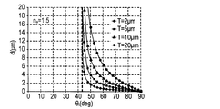
- FIG. 4A is a graph for showing a relationship between a shift amount of X-rays and a tiling angle according to one embodiment of the present invention.
- FIG. 4B is a graph for showing a relationship between a shift amount of X-rays and a tiling angle according to one embodiment of the present invention.
- FIG. 1 is a schematic view of a radiation detector according to one embodiment of the present invention.
- FIG. 2 is a schematic view of an example of a scintillator crystal according to one embodiment of the present invention.
- FIG. 3 is a view for illustrating waveguiding of emitted light of an adhesive layer according to one embodiment of
- FIG. 4C is a graph for showing a relationship between a shift amount of X-rays and a tiling angle according to one embodiment of the present invention.
- FIG. 5A is a view for illustrating an example of arrangement of scintillator crystals according to one embodiment of the present invention.
- FIG. 5B is a view for illustrating another example of arrangement of scintillator crystals according to one embodiment of the present invention.
- FIG. 6 is a schematic view of an example of a radiation measurement system according to one embodiment of the present invention.
- a scintillator plate includes a plurality of scintillator crystals.
- Each of the plurality of scintillator crystals has the above-mentioned phase separation structure, and scintillation light is guided in an extending direction of a first phase.
- the scintillator plate includes a plurality of scintillator crystals each including a plurality of first phases and a second phase present on the periphery of each of the plurality of first phases. It is preferred that the clearance between the plurality of first phases be filled with the second phase.
- the first phase and the second phase are different in refractive index with respect to scintillation light.
- the refractive index of the first phase refers to the refractive index of a material forming the first phase
- the refractive index of the second phase refers to the refractive index of a material forming the second phase.
- the scintillator crystals are joined to each other through intermediation of an adhesive layer.
- the plurality of first phases are present, and an axis (orientation) being the center of gravity of the center axis of each of the plurality of first phases is defined as the center axis of the scintillator crystal.
- the center axis of the scintillator crystal represents the orientation, and a plurality of center axes are present in the scintillator crystal.
- the center axis of the scintillator crystal passing through a certain point thereof is held in contact with the adhesive layer, and an extension line further extending from the center axis toward the adhesive layer side passes through the adhesive layer.
- a center axis of the scintillation crystal and an extension line 107d 1 thereof illustrated in FIG. 1 do not pass through adhesive layers 109c and 109d, but a center axis of the scintillator crystal and an extension line 107d 2 thereof pass through the adhesive layer 109d.
- a scintillator crystal 102d is regarded that at least a part of the extension lines of the center axes thereof passes through the adhesive layer.
- the center axis of the above-mentioned adhesive layer and the center axis of the crystal cross each other, and the adhesive layer is tilted with respect to the center axis of the crystal. Further, when the scintillator plate is used as a radiation detector, the above-mentioned adhesive layer is tilted with respect to the incident direction of radiation.
- an adhesive layer between the scintillator crystals is arranged in substantially parallel to the incident direction of radiation.
- the clearance has an influence on pixels right below the clearance and surrounding pixels thereof.
- the influence of the clearance can be shared by a large number of pixels, and the influence of the clearance on a photographed image can be even more reduced. Further, a dead region can be reduced when the adhesive layer is tilted with respect to the incident direction of radiation.
- the radiation having entered the clearance between the scintillator crystals is not converted into scintillation light and passes through the clearance as the radiation to a light receiving element.
- the scintillator plate according to the present embodiment can reduce or eliminate the dead region.
- FIG. 1 is a schematic view of a radiation detector 100 according to the present embodiment.
- the radiation detector 100 includes a scintillator plate 101 configured to convert radiation 106 (106a, 106b) into scintillation light, and a detection unit 103 configured to detect the scintillation light from the scintillator plate 101.
- the scintillator plate 101 includes a plurality of scintillator crystals 102 (102a to 102e). Each of the scintillator crystals 102 (102a to 102e) includes a plurality of first phases 202 and a second phase 203 present on the periphery of each of the first phases 202 as illustrated in FIG.
- the detection unit 103 includes a substrate 104 and light receiving elements 105 arranged in two directions on the substrate 104, and each light receiving element 105 is configured to detect the intensity of light having entered a light receiving surface thereof.
- the radiation 106 (106a, 106b) is regarded as perpendicularly entering the radiation detector 100, and the radiation 106 (106a, 106b) entering the scintillator crystals 102b and 102c and the adhesive layer 109b between the scintillator crystals 102b and 102c are considered.
- the incident direction of the radiation 106a is matched with the center axis 107c of the scintillator crystal 102c, and emitted light 108a is detected by the detection unit 103.
- emitted light 108b is first generated by the scintillator crystal 102c. Then, the emitted light 108b is guided along the center axis 107c of the scintillator crystal 102c and guided into the scintillator crystal 102b through the adhesive layer 109b.
- the guided light is guided along the center axis 107b of the scintillator crystal 102b together with emitted light 108c generated by the scintillator crystal 102b, and detected by the detection unit 103.
- a dead region with respect to X-rays which corresponds to the adhesive layer 109b, is divided into a plurality of pixels, and a defective pixel is not generated.
- the extension line extending from the center axis of the two adjacent scintillator crystals passes through the adhesive layer, and the adhesive layer is tilted with respect to the incident direction of radiation, the emitted light of the scintillator crystal arranged on an upstream side of the travelling direction of the radiation is guided to the scintillator crystal arranged on a downstream side thereof.
- FIG. 2 is a schematic view of a specific example of a scintillator crystal 201.
- the scintillator crystal 201 has a phase separation structure including a plurality of first phases 202 and a second phase 203 present on the periphery of each of the first phases 202.
- the scintillator crystal 201 has a first surface 208 and a second surface 209, and the first phases 202 extend from the first surface 208 to the second surface 209.
- the first surface 208 serves as a radiation irradiation surface
- the second surface 209 serves as a light extraction surface. Radiation enters the first surface 208, and scintillation light is extracted from the second surface 209 to the light receiving elements.
- At least one of the first phase and the second phase is a light emitting phase for converting at least a part of incident radiation into scintillation light.
- the first phase 202 and the second phase 203 have different refractive indices.
- the scintillation light is guided from the first surface 208 to the second surface 209 and from the second surface 209 to the first surfaced 208 of the scintillator crystal 201 having a thickness 207.
- a higher resolution is provided when the scintillation light is guided in a phase in which the scintillation light is generated. Therefore, it is preferred that a higher refractive index phase having a relatively high refractive index serve as a light emitting phase. In this case, a lower refractive index phase having a relatively low refractive index may or may not serve as a light emitting phase.
- the case where the first phase 202 is a higher refractive index phase and serves as a light emitting phase is hereinafter exemplified.
- the scintillation light is guided between the first surface 208 and the second surface 209 while being confined in the first phase 202, as in an optical fiber.
- the first phase 202 has a cylindrical shape.
- scintillation light 206 that enters the boundary surface between the first phase 202 and the second phase 203 at a critical angle or more is guided through the first phase 202 in a waveguiding direction 210 while repeating total reflection and output from the first surface 208 or the second surface 209.
- the waveguiding direction 210 of the scintillation light is the extending direction (longitudinal direction) of the first phase 202 and is a direction parallel to the center axis of the scintillation light.
- the diameter of the first phase 202 is smaller than the wavelength of the guided emitted light, the scintillation light is not reflected from the boundary surface between the first phase 202 and the second phase 203, and a larger amount of component passes through the boundary surface.
- a period 204 and a diameter 205 of the first phase 202 be larger than the wavelength of the scintillation light.
- a scintillator having a phase separation structure a scintillator having light emission within an ultraviolet range of from 300 nm is used. Therefore, it is desired that the diameter 205 of the first phase 202 be 300 nm or more.
- the diameter 205 of the first phase 202 is larger than the length of a diagonal of one pixel (pixel size) of the light emitting element 105, the influence of confinement of light in one pixel is degraded. Therefore, it is desired that the upper limit value of the diameter 205 of the first phase 202 be smaller than the pixel size.
- the pixel size may be any size, and hence the preferred range of the diameter 205 of the first phase 202 varies depending on the pixel size of a light emitting element to be used.
- the diameter 205 of the first phase 202 fall within a range of from 300 nm to the pixel size.
- the above-mentioned scintillator having a waveguiding function like an optical fiber has a high resolution (also called a space resolution), and a high-resolution sensor having a pixel size of about 2 ⁇ m may also be used.
- a high resolution also called a space resolution
- a high-resolution sensor having a pixel size of about 2 ⁇ m may also be used.
- the diameter of the fiber is more than 2 ⁇ m, light leaks to an adjacent pixel. Therefore, it is desired that the diameter of the first phase 202 be 2 ⁇ m or less.
- the shape of the first phase 202 is not limited to a cylindrical shape, and may be, for example, a polygonal column.
- the largest width of the first phase 202 (width in a diagonal direction when the first phase 202 has a shape of, for example, a quadrangular prism) corresponds to the above-mentioned diameter.
- the first phase 202 linearly continue from the first surface 208 to the second surface 209.
- the first phase 202 is disconnected or branched in the middle; a plurality of crystal phases are integrated; the diameter of the crystal phase changes; and the first phase 202 is not linear and includes a non-linear portion.
- the second phase 203 be present continuously from the first surface 208 to the second surface 209 and that the clearance between the first phases 202 be filled with the second phase 203.
- the difference in refractive index between the first phase 202 and the second phase 203 there is no particular limitation on the difference in refractive index between the first phase 202 and the second phase 203.
- the difference in refractive index be large because the critical angle can be reduced in that case based on the Snell's law.
- a value (also called a refractive index ratio) obtained by dividing the refractive index of a lower refractive index phase by the refractive index of a higher refractive index phase is preferably 0.95 or less, more preferably 0.9 or less.
- the refractive index of the lower refractive index phase or the higher refractive index phase is defined as a refractive index of the material of the lower refractive index phase or the higher refractive index phase at a center wavelength of the scintillation light.
- a scintillator having a eutectic phase separation structure may be used as the scintillator crystal having the structure illustrated in FIG. 2, for example, a scintillator having a eutectic phase separation structure may be used.
- the eutectic phase separation structure refers to a phase separation structure as illustrated in FIG. 2 in which the first phase and the second phase form a eutectic.
- a first phase (GdAlO 3 having a refractive index of 2.05) has a refractive index higher than that of a second phase (Al 2 O 3 having a refractive index of 1.79), and the first phase serves as a scintillator. Therefore, of eutectic phase separation structures, the above-mentioned eutectic phase separation structure has a particularly high waveguiding property.
- the first phase is a crystal of a first material
- the second phase is a crystal of a second material.
- the composition ratio between the material of the first phase and the material of the second phase is not necessarily required to be strictly the eutectic composition ratio.
- the allowable range of the composition ratio can be substantially set to a range of eutectic composition ⁇ 5 mol% with respect to the composition ratio although the range changes depending on the production method of the eutectic.
- a crystal having the phase separation structure of good quality as illustrated in FIG. 2 can be obtained by performing unidirectional solidification through use of a melt in which the material of the first phase and the material of the second phase are mixed in the vicinity of a eutectic composition ratio ( ⁇ 5 mol%).
- a specific method for unidirectional solidification the Bridgman method or the like can be used.
- this structure is regarded as a eutectic phase separation structure.
- the excessive material of the material of the first phase and the material of the second phase may be first precipitated, and the remaining melt may fall within the range of eutectic composition ratio ⁇ 5 mol%.
- the phase separation structure is disturbed at the beginning of solidification, but the phase separation structure of good quality can be obtained along the way. Therefore, it is sufficient that a portion in which the structure is disturbed be appropriately cut off. That is, a load value is not necessarily required to be matched with the composition ratio of the eutectic phase separation structure and may be slightly different therefrom.
- an emission wavelength changes depending on the kinds of elements of emission centers.
- Tb 3+ , Eu 3+ , and Ce 3+ that are rare-earth elements can be used as the emission centers.
- Elements containing those ions are not limited to a simple substance, and it is sufficient that those elements be contained and a compound containing those elements be added as the emission centers. Further, in order to enhance emission efficiency, it is preferred that GdAlO 3 contain the emission centers in an amount of 0.001 mol% or more.
- the total amount of the emission centers be 0.001 mol% or more.
- the addition elements serving as the emission centers are added so as to substitute a Gd site of GdAlO 3 that is the first phase.
- the addition elements are represented by a general formula RE, the composition ratio between Gd 1-x RE x AlO 3 and Al 2 O 3 is 46:54 (mol%).
- Tb 3+ When Tb 3+ is used as the emission center, a green emission peak is exhibited in the vicinity of 545 nm. Further, when Eu 3+ is used as the emission center, a red emission peak is exhibited in the vicinity of 615 nm. Further, when Ce 3+ is used as the emission center, broad ultraviolet light emission is exhibited in the vicinity of 360 nm.
- addition elements other rare-earth elements (Pr, Nd, Pm, Sm, Dy, Ho, Er, Tm, and Yb) may also be selected.
- a radiation detector that realizes a high resolution can be obtained. Meanwhile, a decrease in resolution caused by the incidence of X-rays along the adhesive layer appears more remarkably in a radiation detector having a high resolution. That is, about 10 ⁇ m of a dead region caused by the adhesive layer, which can be relatively ignored in a radiation detector having a resolution of about 100 ⁇ m, is observed remarkably as a defective pixel in a radiation detector having a resolution of 10 ⁇ m or less, for example, about 2 ⁇ m.
- the influence of a defective pixel caused by the adhesive layer is reduced by tiling scintillator crystals with the adhesive layer of the scintillator being tilted with respect to the incident direction of radiation.
- the scintillator plate 101 includes the plurality of scintillator crystals 102 (102a to 102e).
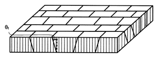
- the two adjacent scintillator crystals 102 are tiled and fixed through intermediation of the adhesive layer.
- the scintillator crystals 102 are tiled so that emitted light of the scintillator crystal close to the incident direction of radiation is guided to the scintillator crystal far away from the incident direction of radiation.
- Radiation 300 enters a scintillator crystal 301a to generate scintillation emission light at an emission point 303a.
- the incident direction of the radiation 300 is matched with the waveguiding direction of the scintillator crystal 301a, and emitted light 304a guided through the scintillator crystal 301a enters an adhesive layer 302 along the waveguiding direction matched with a center axis 305 of the scintillator crystal 301a.
- the emitted light 304a is guided through GdAlO 3 (refractive index: 2.05) serving as the first phase and enters the adhesive layer 302.
- the adhesive layer 302 for example, an epoxy resin (refractive index: 1.55 to 1.61), a melamine resin (refractive index: 1.6), polystyrene (refractive index: 1.6), a vinylidene chloride resin (refractive index: 1.61), polycarbonate (refractive index: 1.59), or the like can be used.
- the refractive index of GdAlO 3 is high as described above, and hence an adhesive layer to be used generally has a relatively low refractive index.
- emitted light 304c guided through the adhesive layer 302 is bent so as to satisfy ⁇ a > ⁇ s .
- the incident angle ⁇ s is larger than a critical angle, that is, the tiling angle ⁇ t is too small, the emitted light 304a is totally reflected without entering the adhesive layer 302.
- the refractive index n s is 2.05.
- the critical tiling angle ⁇ tc at the refractive index n a of 1.5 is 43.0°
- the critical tiling angle ⁇ tc at the refractive index n a of 1.6 is 38.7°
- the critical tiling angle ⁇ tc at the refractive index n a of 1.7 is 34.0°.
- the critical tiling angle ⁇ tc decreases.
- the emitted light 304c guided through the adhesive layer 302 enters the scintillator crystal 301b and is refracted. Then, the emitted light 304c becomes emitted light 304b guided through the scintillator crystal 301b and is detected by a light receiving element. Meanwhile, the radiation 300 generates scintillation emission light also at an emission point 303b. Then, the scintillation emission light generates emitted light 304d guided through the scintillator crystal 301b, and the emitted light 304d is detected by a light receiving element.
- FIG. 4A to FIG. 4C there are shown results obtained by calculating the tiling angle ⁇ t and the shift amount d, when a GdAlO 3 -Al 2 O 3 eutectic is used as a scintillator layer and an adhesive layer having n a of 1.5, 1.6, or 1.7 is used, with respect to the case where the thickness T of the adhesive layer is 2 ⁇ m, 5 ⁇ m, 10 ⁇ m, and 20 ⁇ m.
- the shift amount d tends to decrease.
- the shift amount d is set to be smaller than one pixel of a light emitting element, substantial blurring can be removed.
- the GdAlO 3 -Al 2 O 3 eutectic scintillator has a high resolution, and a high-resolution sensor having a pixel size of, for example, about 2 ⁇ m can also be used.
- a high-resolution sensor having a pixel size of, for example, about 2 ⁇ m can also be used.
- n a refractive index
- the adhesive layer having a refractive index n a of 1.6 in order to set the shift amount d to 2 ⁇ m or less with respect to the thicknesses T of 2 ⁇ m, 5 ⁇ m, 10 ⁇ m, and 20 ⁇ m, it is necessary that the tiling angle ⁇ t be set to be larger than 43°, 52°, 62°, and 72°, respectively.
- the radiation 106 When the radiation 106 is regarded as not perpendicularly entering the radiation detector 100, the radiation enters the radiation detector 100 more diagonally as separating from the center portion of the scintillator plate toward the peripheral portion thereof. Therefore, the decrease in resolution of the peripheral portion can be reduced by tilting the center axis of the scintillator crystal in accordance with the diagonal incidence. In this case, the center axes 107a to 107e of the scintillator crystals are not matched with each other and are tilted more inwardly toward the peripheral portion.
- the present embodiment can be similarly applied to this case by setting the tiling angle ⁇ t to the tilt of the adhesive layer with respect to an intermediate value of the center axes of the adjacent scintillator crystals.
- the tiling angle ⁇ t between the scintillator crystals is set to be constant over the entire scintillator plate, the angle of the adhesive layer with respect to the detection unit 103 is not uniform over the entire scintillator plate.
- the detection unit 103 illustrated in FIG. 1 includes the substrate 104 and the plurality of light receiving elements 105.
- the light receiving elements 105 are arranged on the substrate 104 so as to have two arrangement directions (typically, an x-axis direction and a y-axis direction).
- There is no particular limitation on the light receiving element 105 as long as the light receiving element 105 has a light receiving surface and is configured to detect the intensity of light having entered the light receiving surface, and a CCD image sensor, a CMOS image sensor, or the like can be used.
- the pixel size of the light receiving element 105 there is no particular limitation on the pixel size of the light receiving element 105. However, when the pixel size is 20 ⁇ m or less, the effect of reducing the decrease in resolution, which is provided by the adhesive layer according to the present embodiment, is particularly large.
- the pixel size is preferably 10 ⁇ m or less because the effect is even larger in this case.
- the scintillator crystal 102 and the light receiving elements 105 are held in contact with each other, but may not be held in contact with each other.
- a protective film may be formed between the scintillator crystal 102 and the light receiving elements 105 so that the radiation having passed through the scintillator crystal 102 does not enter the light receiving elements 105.
- the plurality of light receiving elements 105 arranged on one substrate 104 be used as the detection unit 103.
- a plurality of substrates each having a plurality of light receiving elements arranged thereon may also be combined to be used.
- the specific arrangement manner of the scintillator crystals is described.
- the crystals are tiled so that the adhesive layer between the adjacent crystals have a tiling angle larger than the above-mentioned critical tiling angle ⁇ tc .
- the tiling angles ⁇ t are formed so as to be symmetrical with respect to the center portion of the scintillator plate, but all the adhesive surfaces may be tilted in the same direction.
- the adhesive layer be tilted with respect to the incident direction of radiation, and the radiation travels substantially in parallel to the thickness direction of the scintillator plate or travels so as to spread as X-rays 61 of FIG. 6.
- the adhesive layers be tilted so that the center axes thereof cross each other when the center axes are extended toward the detection unit 103.
- the crystals may also be squarely arranged so that the adhesive layers are shifted alternately as illustrated in FIG. 5B. Further, crystals cut out into a polygonal shape may also be arranged. Further, the adhesive layer may not have a flat shape and have a curvature as long as the tiling angle is larger than the critical tiling angle ⁇ tc . Now, a specific example of the present embodiment is described.
- Example 1 In this Example, description is given of a specific example of a method of producing a scintillator crystal and an image pickup result of X-rays when produced scintillator crystals are tiled with the adhesive interface being tilted.
- each scintillator crystal is a eutectic phase separation scintillator crystal containing GdAlO 3 as the material of a plurality of first phases and Al 2 O 3 as the material of a second phase, and contains Tb 3+ as an emission center.
- a method of producing such eutectic phase separation scintillator crystal is described.
- This sample exhibited a green emission peak in the vicinity of 545 nm through X-ray irradiation.
- Two produced samples were caused to adhere to each other through use of an adhesive having a refractive index of 1.5 so that the tiling angle ⁇ t of an adhesive layer reached 60°, to thereby provide a sample having dimensions of 5 mm ⁇ 5 mm ⁇ 500 ⁇ m (thickness). Further, for comparison, a sample having a tiling angle ⁇ t of 0° was also prepared.
- the sample having a tiling angle ⁇ t of 60° was observed with a scanning electronic microscope, and it was confirmed that the sample had a phase separation structure in which an indefinite number of GdAlO 3 columnar structures each having a diameter of about 1.2 ⁇ m were buried in the Al 2 O 3 phase.
- the thickness of the adhesive layer was about 10 ⁇ m. In general, the thickness of the adhesive layer falls within a range of from 3 ⁇ m to 30 ⁇ m.
- an X-ray image pickup system was used, which was capable of acquiring an image having a resolution of one pixel of 0.65 ⁇ m by magnifying a light extraction surface of a scintillator crystal with a lens and forming an image onto a charge-coupled device (CCD) serving as a two-dimensional light receiving element.
- CCD charge-coupled device
- a radiation source an X-ray source of a tungsten tube was used. The radiation source was arranged such that X-rays perpendicularly enter the scintillator crystal, and X-rays obtained under the conditions of 40 kV, 0.5 mA, and the presence of an Al filter were used for image pickup.
- the scintillator crystal having a phase separation structure has a waveguiding property like an optical fiber. Therefore, when such scintillator crystal and a high-resolution sensor having a pixel size of several ⁇ m are used, an X-ray image can be acquired with a high space resolution capable of resolving an image by several ⁇ m. However, an X-ray image can be acquired at a high resolution, and hence the adhesive layer to be tiled is also formed into an image. Thus, when the tiling angle is appropriately set, and adjacent scintillator crystals are tiled while being tilted as in this Example, a radiation detector capable of resolving a pattern of about several ⁇ m over an entire region can be manufactured.
- Example 2 In this Example, description is given of a specific example in which the radiation detector of Example 1 is used as a detector of an X-ray Talbot interferometer serving as a radiation measurement system.
- FIG. 6 is a schematic view for illustrating an X-ray Talbot interferometer of this Example.
- the X-ray Talbot interferometer includes an X-ray source 60, an X-ray diffraction grating configured to diffract X-rays 61 from the X-ray source 60 to form an interference pattern, an X-ray detector 64 configured to detect the X-rays 61 forming the interference pattern, and a computing device 65 configured to obtain information on a subject 62 to be examined, through use of the result of detection by the X-ray detector 64.
- a general Talbot interferometer has a grating called a shield grating or an absorption grating arranged at a position where the interference pattern is to be formed, and is configured to obtain information on an interference pattern having a period of about several ⁇ m by forming a moire.
- the X-ray Talbot interferometer of this Example includes the radiation detector of Example 1 as the X-ray detector 64. Therefore, when the X-ray detector 64 is arranged at a position where an interference pattern is to be formed, the contrast of the interference pattern can be directly observed with the X-ray detector 64. Thus, information on the phase, scattering, and absorption of the subject 62 can be obtained by analyzing a change in interference pattern caused by the subject 62, through use of the result of detection by the X-ray detector 64.
- the other items such as the X-ray source, the diffraction grating, and the method of analyzing an interference pattern with a computing device are the same as those of the general Talbot interferometer.
- the X-ray Talbot interferometer may include a display unit (not shown) configured to display information on a subject obtained by the computing device 65. Further, the X-ray Talbot interferometer may not include the computing device 65 or the X-ray source 60. In this case, image pickup (acquisition of an interference pattern) with the X-ray Talbot interferometer can be performed through combination of any X-ray source during image pickup.
- a scintillator plate capable of reducing the influence of the clearance between scintillator crystals on an X-ray image in a radiation detector using, as a scintillator, a structure including two crystal phases having different refractive indices. Further, a radiation detector including the scintillator plate and a radiation measurement system including the radiation detector can also be provided.
Landscapes
- Physics & Mathematics (AREA)
- Health & Medical Sciences (AREA)
- Life Sciences & Earth Sciences (AREA)
- General Physics & Mathematics (AREA)
- High Energy & Nuclear Physics (AREA)
- Molecular Biology (AREA)
- Spectroscopy & Molecular Physics (AREA)
- Chemical & Material Sciences (AREA)
- Crystallography & Structural Chemistry (AREA)
- Measurement Of Radiation (AREA)
- Conversion Of X-Rays Into Visible Images (AREA)
- Luminescent Compositions (AREA)
Priority Applications (1)
| Application Number | Priority Date | Filing Date | Title |
|---|---|---|---|
| US16/077,592 US10725186B2 (en) | 2016-02-23 | 2017-02-14 | Scintillator plate, radiation detector, and radiation measurement system |
Applications Claiming Priority (2)
| Application Number | Priority Date | Filing Date | Title |
|---|---|---|---|
| JP2016031747A JP6774188B2 (ja) | 2016-02-23 | 2016-02-23 | シンチレータプレート、放射線検出器及び放射線計測システム |
| JP2016-031747 | 2016-02-23 |
Publications (1)
| Publication Number | Publication Date |
|---|---|
| WO2017145858A1 true WO2017145858A1 (en) | 2017-08-31 |
Family
ID=58213275
Family Applications (1)
| Application Number | Title | Priority Date | Filing Date |
|---|---|---|---|
| PCT/JP2017/005260 Ceased WO2017145858A1 (en) | 2016-02-23 | 2017-02-14 | Scintillator plate, radiation detector, and radiation measurement system |
Country Status (3)
| Country | Link |
|---|---|
| US (1) | US10725186B2 (https=) |
| JP (1) | JP6774188B2 (https=) |
| WO (1) | WO2017145858A1 (https=) |
Cited By (1)
| Publication number | Priority date | Publication date | Assignee | Title |
|---|---|---|---|---|
| CN115144888A (zh) * | 2021-03-30 | 2022-10-04 | 西门子医疗有限公司 | 具有无死区的对接的吸收体拼块的辐射检测器 |
Families Citing this family (2)
| Publication number | Priority date | Publication date | Assignee | Title |
|---|---|---|---|---|
| CN109782328B (zh) * | 2019-01-11 | 2021-03-26 | 惠科股份有限公司 | 射线转换器和射线探测平板装置 |
| JP2023077337A (ja) * | 2021-11-24 | 2023-06-05 | キヤノン株式会社 | シンチレータプレート、放射線検出器、およびシンチレータプレートの製造方法 |
Citations (3)
| Publication number | Priority date | Publication date | Assignee | Title |
|---|---|---|---|---|
| US20110139991A1 (en) * | 2009-12-15 | 2011-06-16 | Saint-Gobain Ceramics & Plastics, Inc. | Radiation detection system and method of making a radiation detection system |
| WO2013015454A2 (en) * | 2011-07-27 | 2013-01-31 | Canon Kabushiki Kaisha | Scintillator having a phase separation structure and radiation detector using the same |
| US20130026374A1 (en) * | 2011-07-26 | 2013-01-31 | Canon Kabushiki Kaisha | Radiation detector |
Family Cites Families (17)
| Publication number | Priority date | Publication date | Assignee | Title |
|---|---|---|---|---|
| EP0958508B1 (en) | 1997-02-10 | 2007-03-28 | THE UNIVERSITY OF ALBERTA, SIMON FRASER UNIVERSITY, THE UNIV. OF VICTORIA,THE UNIV. OF BRITISH COLUMBIA, carrying on as TRIUMF | Segmented scintillation detector for photon interaction coordinates |
| JP4693297B2 (ja) * | 2000-08-10 | 2011-06-01 | キヤノン株式会社 | 放射線撮像装置および放射線撮像システム |
| US6800857B2 (en) | 2000-08-10 | 2004-10-05 | Canon Kabushiki Kaisha | Large-area fiber plate, radiation image pickup apparatus utilizing the same and producing method therefor |
| JP4647828B2 (ja) * | 2001-05-07 | 2011-03-09 | 浜松ホトニクス株式会社 | シンチレータパネルおよびそれを用いた放射線検出器 |
| AU2003221365A1 (en) | 2002-03-15 | 2003-09-29 | Canon Kabushiki Kaisha | Porous material and process for producing the same |
| AU2003213353A1 (en) | 2002-03-15 | 2003-09-29 | Canon Kabushiki Kaisha | Porous material and process for producing the same |
| JP5174180B2 (ja) | 2008-10-29 | 2013-04-03 | キヤノン株式会社 | X線撮像装置およびx線撮像方法 |
| US8559594B2 (en) | 2008-10-29 | 2013-10-15 | Canon Kabushiki Kaisha | Imaging apparatus and imaging method |
| JP5121960B2 (ja) | 2011-03-30 | 2013-01-16 | キヤノン株式会社 | 相分離構造を有するシンチレータ結晶体 |
| JP5138104B2 (ja) | 2011-03-30 | 2013-02-06 | キヤノン株式会社 | 多孔質シンチレータ結晶体 |
| JP5767512B2 (ja) | 2011-06-07 | 2015-08-19 | キヤノン株式会社 | 放射線検出素子及び放射線検出器 |
| US8586931B2 (en) | 2011-07-12 | 2013-11-19 | Canon Kabushiki Kaisha | Scintillator having phase separation structure and radiation detector using the same |
| JP2013019796A (ja) | 2011-07-12 | 2013-01-31 | Canon Inc | 放射線検出器 |
| JP2013024731A (ja) | 2011-07-21 | 2013-02-04 | Canon Inc | 放射線検出装置 |
| JP5901169B2 (ja) | 2011-07-26 | 2016-04-06 | キヤノン株式会社 | シンチレータ構造体および放射線検出器 |
| JP6289157B2 (ja) | 2013-03-05 | 2018-03-07 | キヤノン株式会社 | シンチレータ及び放射線検出器 |
| JP2015111107A (ja) * | 2013-10-28 | 2015-06-18 | 国立大学法人東北大学 | シンチレータおよび放射線検出器 |
-
2016
- 2016-02-23 JP JP2016031747A patent/JP6774188B2/ja active Active
-
2017
- 2017-02-14 WO PCT/JP2017/005260 patent/WO2017145858A1/en not_active Ceased
- 2017-02-14 US US16/077,592 patent/US10725186B2/en active Active
Patent Citations (4)
| Publication number | Priority date | Publication date | Assignee | Title |
|---|---|---|---|---|
| US20110139991A1 (en) * | 2009-12-15 | 2011-06-16 | Saint-Gobain Ceramics & Plastics, Inc. | Radiation detection system and method of making a radiation detection system |
| US20130026374A1 (en) * | 2011-07-26 | 2013-01-31 | Canon Kabushiki Kaisha | Radiation detector |
| JP2013024833A (ja) | 2011-07-26 | 2013-02-04 | Canon Inc | 放射線検出器 |
| WO2013015454A2 (en) * | 2011-07-27 | 2013-01-31 | Canon Kabushiki Kaisha | Scintillator having a phase separation structure and radiation detector using the same |
Cited By (2)
| Publication number | Priority date | Publication date | Assignee | Title |
|---|---|---|---|---|
| CN115144888A (zh) * | 2021-03-30 | 2022-10-04 | 西门子医疗有限公司 | 具有无死区的对接的吸收体拼块的辐射检测器 |
| US12433044B2 (en) | 2021-03-30 | 2025-09-30 | Siemens Healthineers Ag | Apparatuses for radiation detection including absorber tiles with a semiconductor material or a perovskite material disposed between the absorber tiles and methods of manufacturing the same |
Also Published As
| Publication number | Publication date |
|---|---|
| US20190033472A1 (en) | 2019-01-31 |
| JP6774188B2 (ja) | 2020-10-21 |
| US10725186B2 (en) | 2020-07-28 |
| JP2017150868A (ja) | 2017-08-31 |
Similar Documents
| Publication | Publication Date | Title |
|---|---|---|
| US9068111B2 (en) | Scintillator having a phase separation structure and radiation detector using the same | |
| JP5646906B2 (ja) | X線装置およびx線測定方法 | |
| JP5587788B2 (ja) | 複合樹脂におけるシンチレータを備えた放射線感受性検出器 | |
| US9360566B2 (en) | Radiation detector | |
| CN113169014B (zh) | 用于检测x射线的高分辨率光阀检测器 | |
| JP2013152160A (ja) | 放射線撮像装置及び放射線撮像システム | |
| US10725186B2 (en) | Scintillator plate, radiation detector, and radiation measurement system | |
| KR20150058190A (ko) | 신틸레이터 패널, 및 방사선 검출기 | |
| JP2017133894A (ja) | シンチレータアレイ、それを用いたx線検出器およびx線検査装置 | |
| US12498496B2 (en) | Radiation imaging system and radiation imaging method | |
| EP2775319B1 (en) | Scintillator having a phase separation structure and radiation detector using the same | |
| JP6622572B2 (ja) | 放射線計測システム、及びトールボット干渉計 | |
| Yao et al. | Fabrication and performance of CsI (Tl) scintillation films with pixel-like columnar-matrix structure | |
| JP6949479B2 (ja) | シンチレータプレート、放射線検出器及び放射線計測システム | |
| JP5645584B2 (ja) | 放射線センサー | |
| Graafsma et al. | Detectors for synchrotron tomography | |
| WO2019226859A1 (en) | Flat panel x-ray imager with scintillating glass substrate | |
| US7414245B2 (en) | Scintillator-based micro-radiographic imaging device | |
| Ullherr et al. | Quantitative optimization of X-ray image acquisition with respect to object thickness and anode voltage—A comparison using different converter screens | |
| JP6289033B2 (ja) | 放射線検出器 | |
| JP2018075173A (ja) | X線撮像装置 | |
| Ishikawa et al. | High-speed, high-resolution, three-dimensional imaging of threading dislocations in β-Ga2O3 via phase-contrast microscopy | |
| RU197875U1 (ru) | Детектор рентгеновского излучения с составным сцинтиллятором | |
| WO2006113933A2 (en) | Scintillator-based micro-radiographic imaging device | |
| Miyamoto et al. | Ultra-compact imaging plate scanner module using a MEMS mirror and specially designed MPPC |
Legal Events
| Date | Code | Title | Description |
|---|---|---|---|
| NENP | Non-entry into the national phase |
Ref country code: DE |
|
| 121 | Ep: the epo has been informed by wipo that ep was designated in this application |
Ref document number: 17708592 Country of ref document: EP Kind code of ref document: A1 |
|
| 122 | Ep: pct application non-entry in european phase |
Ref document number: 17708592 Country of ref document: EP Kind code of ref document: A1 |