WO2017138284A1 - 絶縁電線 - Google Patents
絶縁電線 Download PDFInfo
- Publication number
- WO2017138284A1 WO2017138284A1 PCT/JP2017/000614 JP2017000614W WO2017138284A1 WO 2017138284 A1 WO2017138284 A1 WO 2017138284A1 JP 2017000614 W JP2017000614 W JP 2017000614W WO 2017138284 A1 WO2017138284 A1 WO 2017138284A1
- Authority
- WO
- WIPO (PCT)
- Prior art keywords
- insulating layer
- insulated wire
- varnish
- silicone
- conductor
- Prior art date
- Legal status (The legal status is an assumption and is not a legal conclusion. Google has not performed a legal analysis and makes no representation as to the accuracy of the status listed.)
- Ceased
Links
Images

Classifications
-
- H—ELECTRICITY
- H01—ELECTRIC ELEMENTS
- H01B—CABLES; CONDUCTORS; INSULATORS; SELECTION OF MATERIALS FOR THEIR CONDUCTIVE, INSULATING OR DIELECTRIC PROPERTIES
- H01B7/00—Insulated conductors or cables characterised by their form
- H01B7/02—Disposition of insulation
Definitions
- the present invention relates to an insulated wire.
- the present invention claims priority based on Japanese Patent Application No. 2016-024006 filed on Feb. 10, 2016, and incorporates all the contents described in the Japanese application.
- a high voltage is applied to an insulated wire constituting the electric device, and partial discharge (corona discharge) is likely to occur on the surface of the insulating film.
- partial discharge corona discharge
- a local temperature rise, ozone generation, ion generation, or the like is caused in the insulated wire due to the generation of corona discharge, dielectric breakdown occurs at an early stage. This shortens the life of the insulated wire and thus the electrical equipment.
- the insulated wire used for the electric equipment with a high applied voltage is also required to improve the corona discharge starting voltage in addition to excellent insulation and mechanical strength.
- An effective way to increase the corona discharge starting voltage is to reduce the dielectric constant of the insulating coating.
- a heat-cured film (insulating coating) is formed by an insulating varnish containing a coating film constituent resin and a thermally decomposable resin that decomposes at a temperature lower than the baking temperature of the coating film constituent resin )
- JP 2012-224714 A a heat-cured film
- pores are formed in the heat-cured film by utilizing the fact that the thermally decomposable resin is thermally decomposed during baking of the coating film constituting resin and the portion becomes pores. Low dielectric constant of insulating coating is realized.
- overvoltage may be temporarily applied to insulated wires during use.
- surge voltage When surge voltage is applied, the insulating layer deteriorates due to heat dissipation and the product life is shortened. Therefore, an insulated wire has been proposed in which inorganic fine particles (silica) are contained in the insulating layer to improve surge resistance (see Japanese Patent Application Laid-Open No. 2007-141507).
- An insulated wire according to one aspect of the present invention made to solve the above problems is an insulated wire comprising a linear conductor and one or more insulating layers laminated on the outer peripheral surface of the conductor,
- the insulating layer contains silicone.
- the present invention has been made on the basis of the above circumstances, and an object thereof is to provide an insulated wire excellent in surge resistance while maintaining manufacturability.
- the insulated wire of the present invention is excellent in surge resistance while maintaining manufacturability.
- the insulated wire which concerns on 1 aspect of this invention is an insulated wire provided with a linear conductor and 1 or several insulating layer laminated
- the said insulating layer contains silicone.
- the insulated wire contains silicone in the insulating layer. This silicone is modified to silica by heat dissipation when a surge voltage is applied. Silicone contained in the insulating layer is unlikely to be unevenly distributed in the insulating layer unlike silica, and is denatured into silica after heat dissipation. Therefore, the insulated wire contains silicon and maintains the manufacturability, while improving the surge resistance of the insulating layer uniformly, and can significantly improve the product life. “Silicone” means a polymer containing a repeating structure of a siloxane bond in which a silicon atom and an oxygen atom are bonded.
- At least one of the insulating layers contains a matrix and silicone dispersed in the matrix.
- surge resistance can be improved easily and reliably by the silicone containing and dispersing the silicone in the matrix.
- At least one of the insulating layers may contain silicone as a main component.
- the insulating layer includes a layer mainly composed of silicone, surge resistance can be easily and reliably improved.
- At least one of the insulating layers may contain a plurality of pores and an outer shell around the pores, and the outer shell may contain silicone as a main component.
- the insulating layer contains such pores and outer shells, surge resistance can be improved while lowering the dielectric constant of the insulating layer.
- the pores included in the insulating layer are surrounded by the outer shell, the pores are difficult to communicate with each other and coarse pores are not easily generated. Therefore, the dielectric constant can be reduced while suppressing a decrease in insulation and solvent resistance.
- the “main component” means a component that is contained most, for example, a component that is contained in an amount of 50% by mass or more.
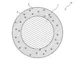
- the insulated wire 10 in FIG. 1 includes a linear conductor 1 and a single insulating layer 2 laminated on the outer peripheral surface of the conductor 1.
- the insulating layer 2 contains a matrix and silicone 3 dispersed in the matrix.
- the conductor 1 is, for example, a round wire having a circular cross section, but may be a square wire having a square cross section or a stranded wire obtained by twisting a plurality of strands.
- the material of the conductor 1 is preferably a metal having high electrical conductivity and high mechanical strength.
- metals include copper, copper alloys, aluminum, nickel, silver, soft iron, steel, and stainless steel.
- the conductor 1 is a material in which these metals are formed in a linear shape, or a multilayer structure in which such a linear material is coated with another metal, such as a nickel-coated copper wire, a silver-coated copper wire, or a copper-coated aluminum. Wire, copper-coated steel wire, etc. can be used.
- the insulating layer 2 contains a matrix and silicone 3 dispersed in the matrix.
- the lower limit of the average thickness of the insulating layer 2 is preferably 5 ⁇ m and more preferably 10 ⁇ m.
- the upper limit of the average thickness of the insulating layer 2 is preferably 200 ⁇ m, and more preferably 100 ⁇ m. If the average thickness of the insulating layer 2 is less than the lower limit, the insulating layer 2 may be broken and the conductor 1 may be insufficiently insulated. Conversely, when the average thickness of the insulating layer 2 exceeds the above upper limit, the volume efficiency of a coil or the like formed using the insulated wire 10 may be lowered.
- the matrix of the insulating layer 2 is formed of a resin other than the silicone 3.
- the main component (main polymer) of the matrix is not particularly limited, but when a thermosetting resin is used, for example, polyvinyl formal, thermosetting polyurethane, thermosetting acrylic resin, epoxy resin, phenoxy resin, thermosetting Curable polyester, thermosetting polyester imide, thermosetting polyester amide imide, thermosetting polyamide imide, thermosetting polyimide and the like can be used.
- a thermoplastic resin as a main polymer, polyether imide, polyether ether ketone, polyether sulfone, thermoplastic polyimide etc. can be used, for example.
- thermosetting polyimide is preferable in that it can easily apply the varnish for forming the insulating layer and can easily improve the strength and heat resistance of the insulating layer 2.
- Silicone 3 is in the form of particles and is dispersed in the matrix.
- the shape of the silicone 3 may be spherical or flat.
- silicone for example, organopolysiloxane such as polymethylsiloxane is used.
- the lower limit of the average particle size of silicone 3 is not particularly limited, but is preferably 0.1 ⁇ m, more preferably 1 ⁇ m, and even more preferably 1.5 ⁇ m.
- the upper limit of the average particle diameter of the silicone 3 is preferably 10 ⁇ m, more preferably 8 ⁇ m, and even more preferably 6 ⁇ m.
- the average particle diameter of the silicone 3 is smaller than the above lower limit, the dispersibility is lowered, and the effect of improving surge resistance may be lowered.
- the average particle diameter of the silicone 3 exceeds the above upper limit, the insulating layer 2 may become unnecessarily thick in addition to the risk that the dielectric constant of the insulating layer 2 will increase or the mechanical strength will decrease.
- the “average particle size” means a particle size indicating the highest volume content in the particle size distribution measured with a laser diffraction particle size distribution analyzer.
- the content of the silicone 3 in the insulating layer 2 can be arbitrarily changed according to the overvoltage (surge voltage) and life time assumed when the insulated wire is used.
- As an upper limit of the content rate of the silicone 3 in the insulating layer 2 60 mass parts is preferable with respect to 100 mass parts of matrices, 50 mass parts is more preferable, and 40 mass parts is further more preferable.
- the content rate of silicone 3 is smaller than the said minimum, there exists a possibility that the improvement effect of surge resistance may become inadequate.
- the content rate of the silicone 3 exceeds the above upper limit, the dielectric constant of the insulating layer 2 may increase, the mechanical strength, and the like may decrease.
- the content rate in the whole insulating layer 2 of silicone 3 in insulating layer 2 As a minimum of the content rate in the whole insulating layer 2 of silicone 3 in insulating layer 2, 3 mass% is preferred, 10 mass% is more preferred, and 15 mass% is still more preferred. On the other hand, as an upper limit of the content rate in the whole insulating layer 2 of the silicone 3 in the insulating layer 2, 50 mass% is preferable, 40 mass% is more preferable, and 30 mass% is further more preferable.
- the content rate of silicone 3 is smaller than the said minimum, there exists a possibility that the improvement effect of surge resistance may become inadequate.
- the content rate of silicone 3 exceeds the said upper limit, in addition to the possibility that the mechanical strength etc. of the insulating layer 2 will fall, there exists a possibility that the insulating layer 2 may become thick.
- a curing agent may be contained in the resin composition forming the insulating layer 2.
- Curing agents include titanium-based curing agents, isocyanate compounds, blocked isocyanates, urea and melamine compounds, amino resins, acetylene derivatives, alicyclic acid anhydrides such as methyltetrahydrophthalic anhydride, aliphatic acid anhydrides, and aromatics. An acid anhydride etc. are illustrated.
- These curing agents are appropriately selected according to the type of main polymer contained in the resin composition to be used. For example, in the case of polyamideimide, imidazole, triethylamine and the like are preferably used as the curing agent.
- examples of the titanium-based curing agent include tetrapropyl titanate, tetraisopropyl titanate, tetramethyl titanate, tetrabutyl titanate, and tetrahexyl titanate.
- isocyanate compounds include aromatic diisocyanates such as tolylene diisocyanate (TDI), diphenylmethane isocyanate (MDI), p-phenylene diisocyanate, naphthalene diisocyanate, hexamethylene diisocyanate (HDI), 2,2,4-trimethylhexane diisocyanate, C3-C12 aliphatic diisocyanates such as lysine diisocyanate, 1,4-cyclohexane diisocyanate (CDI), isophorone diisocyanate (IPDI), 4,4'-dicyclohexylmethane diisocyanate (hydrogenated MDI), methylcyclohexane diisocyanate, isopropylidene Dicyclohexyl-4,4′-diisocyanate, 1,3-diisocyanatomethylcyclohexane (hydrogenated XD ), Hydrogenated TDI,
- blocked isocyanate examples include diphenylmethane-4,4′-diisocyanate (MDI), diphenylmethane-3,3′-diisocyanate, diphenylmethane-3,4′-diisocyanate, diphenylether-4,4′-diisocyanate, and benzophenone-4,4.
- MDI diphenylmethane-4,4′-diisocyanate
- diphenylmethane-3,3′-diisocyanate diphenylmethane-3,4′-diisocyanate
- diphenylether-4,4′-diisocyanate diphenylether-4,4′-diisocyanate
- benzophenone-4,4 examples include benzophenone-4,4.
- melamine compound examples include methylated melamine, butylated melamine, methylolated melamine, and butyrololized melamine.
- acetylene derivative examples include ethynylaniline and ethynylphthalic anhydride.
- the method of manufacturing the insulated wire 10 includes a step of preparing an insulating layer forming varnish by dispersing silicone 3 in a resin composition obtained by diluting the resin forming the insulating layer 2 with a solvent (varnish preparing step); A step of applying and heating the insulating layer forming varnish to the outer peripheral surface of the conductor 1 (varnish applying step).
- varnish preparation process In the varnish preparation step, first, a resin composition that forms the matrix of the insulating layer 2 is prepared by diluting the resin that forms the matrix of the insulating layer 2 (a precursor in the case of a thermosetting resin) with a solvent. . Next, silicone 3 is dispersed in this resin composition to prepare an insulating layer forming varnish. Instead of dispersing the silicone 3 in the resin composition, the insulating layer forming varnish may be prepared by simultaneously mixing the silicone 3 when the resin is diluted with a solvent.
- the diluting solvent a known organic solvent conventionally used for insulating varnish can be used. Specifically, polar organic solvents such as N-methyl-2-pyrrolidone, N, N-dimethylacetamide, N, N-dimethylformamide, dimethyl sulfoxide, tetramethylurea, hexaethylphosphoric triamide, ⁇ -butyrolactone and the like are used.
- ketones such as acetone, methyl ethyl ketone, methyl isobutyl ketone, cyclohexanone, esters such as methyl acetate, ethyl acetate, butyl acetate, diethyl oxalate, diethyl ether, ethylene glycol dimethyl ether, diethylene glycol monomethyl ether, ethylene glycol monobutyl ether (butyl cellosolve) ), Ethers such as diethylene glycol dimethyl ether and tetrahydrofuran, hydrocarbons such as hexane, heptane, benzene, toluene and xylene , Halogenated hydrocarbons such as dichloromethane and chlorobenzene, phenols such as cresol and chlorophenol, and tertiary amines such as pyridine. These organic solvents may be used alone or in combination of two or more. Used.
- the lower limit of the resin solid content concentration of the insulating layer forming varnish is preferably 15% by mass, and more preferably 20% by mass.
- the upper limit of the resin solid content concentration of the insulating layer forming varnish is preferably 50% by mass, and more preferably 30% by mass.
- varnish application step first, the insulating layer forming varnish prepared in the varnish preparation step is applied to the outer peripheral surface of the conductor 1, and then the application amount of the varnish of the conductor 1 is adjusted and the applied varnish surface of the conductor 1 is applied. Perform smoothing.
- the coating die has an opening.
- the conductor 1 coated with the insulating layer forming varnish passes through the opening, the excess varnish is removed, and the coating amount of the varnish is adjusted. Thereby, as for the said insulated wire 10, the thickness of the insulating layer 2 becomes uniform and uniform electrical insulation is obtained.
- the insulating layer 2 is formed on the surface of the conductor 1 by passing the conductor 1 coated with the insulating layer forming varnish through a baking furnace and baking the insulating layer forming varnish.
- the insulated wire 10 is obtained.
- the silicone 3 dispersed in the matrix of the insulating layer 2 is denatured into silica by heat dissipation when a surge voltage is applied.
- This silica can improve surge resistance and suppress deterioration of the insulating layer 2 due to surge voltage. Accordingly, since the insulated wire 10 has silica derived from the silicone 3 in the insulating layer 2 after being radiated, the surge resistance of the insulating layer 2 is uniformly increased while maintaining the manufacturability and the product life is increased. It can be remarkably improved.
- the insulating layer 2 may have a multilayer structure. In this case, at least one layer of the insulating layer 2 may contain the silicone 3.
- the insulated wire 20 in FIG. 2 includes a linear conductor 1 and a multilayer insulating layer 22 laminated on the outer peripheral surface of the conductor 1.
- the insulating layer 22 has an inner layer 22a and an outer layer 22b. Since the conductor 1 is the same as the conductor 1 of the insulated wire 10 of FIG. 1, it attaches
- the insulating layer 22 has an inner layer 22a laminated on the outer circumferential surface of the conductor 1, and an outer layer 22b laminated on the outer circumferential surface of the inner layer 22a and forming the outermost layer.
- the outer layer 22b is mainly composed of silicone.
- the outer layer 22b may contain other insulating resins and additives in addition to silicone.
- the content rate of silicone in outer layer 22b As a minimum of the content rate of silicone in outer layer 22b, 2 mass% is preferred and 5 mass% is still more preferred.
- the upper limit of the silicone content in the outer layer 22b is not particularly limited, and is usually 100% by mass. When the content rate of silicone is smaller than the said minimum, there exists a possibility that the improvement effect of surge resistance may become inadequate.
- the lower limit of the average thickness of the outer layer 22b is preferably 1 ⁇ m and more preferably 3 ⁇ m.
- the upper limit of the average thickness of the outer layer 22b is preferably 200 ⁇ m, and more preferably 100 ⁇ m. If the average thickness of the outer layer 22b is less than the lower limit, the effect of improving surge resistance may be insufficient. Conversely, when the average thickness of the outer layer 22b exceeds the above upper limit, the dielectric constant of the insulating layer 2 may increase, or the volume efficiency of a coil or the like formed using the insulated wire 20 may be reduced.
- the inner layer 22a is formed of an insulating resin composition.
- this resin composition it can be set as the same as the resin composition which forms the insulating layer 2 of the insulated wire 10 of FIG. 1, for example.
- the resin composition forming the inner layer 22a may or may not contain silicone.
- the lower limit of the average thickness of the inner layer 22a is preferably 5 ⁇ m and more preferably 10 ⁇ m.
- the upper limit of the average thickness of the inner layer 22a is preferably 200 ⁇ m, and more preferably 100 ⁇ m.
- the average thickness of the inner layer 22a is less than the lower limit, the inner layer 22a may be broken and the conductor 1 may be insufficiently insulated.
- the average thickness of the inner layer 22a exceeds the upper limit, the volume efficiency of a coil or the like formed using the insulated wire 20 may be lowered.
- the insulated wire 20 is formed by applying and heating a resin composition obtained by diluting a resin or the like for forming the inner layer 22a with a solvent on the outer peripheral surface of the conductor 1 (inner varnish applying step), and forming the outer layer 22b. And a step of applying and heating a resin composition obtained by diluting a resin or the like with a solvent to the outer peripheral surface of the inner layer 22a (outer layer varnish applying step).
- the silicone contained in the inner layer 22a is denatured into silica by heat dissipation when a surge voltage is applied. Accordingly, since the silica derived from silicone is present in the insulating layer 22 after the heat dissipation once, the insulated wire 20 uniformly improves the surge resistance of the insulating layer 22 while maintaining the manufacturability, thereby extending the product life. It can be remarkably improved.
- the insulating layer 2 may have a multilayer structure of three or more layers, and the layer mainly composed of silicone is not limited to the outermost layer, and may be an innermost layer or an intermediate layer. . *
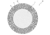
- the insulated wire 30 in FIG. 3 includes a linear conductor 1 and a single insulating layer 32 laminated on the outer peripheral surface of the conductor 1.
- the insulating layer 32 includes a plurality of pores 4 and an outer shell 5 at the peripheral edge of the pores. Since the conductor 1 is the same as the conductor 1 of the insulated wire 10 of FIG. 1, it attaches
- the insulating layer 32 contains a plurality of pores 4 derived from hollow-forming particles having a core-shell structure, which will be described later, and an outer shell 5 mainly composed of silicone.
- the insulating layer 32 is formed of an insulating resin composition, pores 4 scattered in the resin composition, and an outer shell 5 at the peripheral edge of the pores 4.
- this resin composition it can be set to be the same as that of the resin composition which forms the insulating layer 2 of the insulated wire 10 of FIG.
- the resin composition forming the insulating layer 32 may or may not contain silicone.
- the plurality of pores 4 are each covered with an outer shell 5 as shown in FIG. 3, and the outer shell 5 is constituted by a shell that has been hollowed by removing the core of the core-structured hollow forming particles. That is, the outer shell 5 is derived from a shell of hollow-forming particles having a core-shell structure. Further, at least a part of the plurality of outer shells 5 has a defect.
- the plurality of pores 4 are preferably flat spheres as shown in FIG.
- the minor axis of the pore 4 when the minor axis of the pore 4 is oriented in the direction perpendicular to the surface of the conductor 1, the pores are less likely to come into contact with each other in the vertical direction in which external force is likely to act, so that the independent pores are more easily maintained. Therefore, the larger the proportion of the pores 4 whose minor axis is oriented in the direction perpendicular to the surface of the conductor 1, the better.
- the lower limit of the ratio of the number of pores 4 whose minor axis is oriented in the direction perpendicular to the surface of the conductor 1 with respect to the total number of pores 4 is preferably 60%, more preferably 80%.
- the ratio of the pores 4 whose minor axis is oriented in the direction perpendicular to the surface of the conductor 1 is less than the above lower limit, the pores 4 that come into contact with the pores may increase, and the generation of continuous pores may not be sufficiently suppressed.
- the lower limit of the ratio of the length of the minor axis to the major axis in the cross section including the minor axis and the major axis of the pore 4 is preferably 0.2, and more preferably 0.3.
- the upper limit of the average of the above ratio is preferably 0.95, more preferably 0.9. If the average of the above ratios is less than the lower limit, it is necessary to increase the amount of shrinkage in the thickness direction during varnish baking, which may reduce the flexibility of the insulated wire 30. On the contrary, when the average of the ratio exceeds the upper limit, when the porosity is increased, the pores are easily brought into contact with each other in the thickness direction of the insulating layer 32 where the external force easily acts, and the communication suppression effect of the pores 4 is obtained.
- the ratio can be adjusted by changing the pressure applied to the hollow particles by shrinkage during baking of the resin composition contained in the insulating layer forming varnish.
- the pressure applied to the hollow forming particles can be changed depending on, for example, the type of the material that is the main component of the resin composition, the thickness of the insulating layer 32, the material of the hollow forming particles, the baking conditions, and the like.
- the lower limit of the average major axis of the pores 4 is preferably 0.1 ⁇ m, and more preferably 1 ⁇ m.
- the upper limit of the average of the major axis is preferably 10 ⁇ m, and more preferably 8 ⁇ m. If the average of the major axis is less than the lower limit, the insulating layer 32 may not have a desired porosity. On the contrary, if the average of the major axis exceeds the upper limit, it is difficult to make the distribution of the pores 4 in the insulating layer 32 uniform, and the dielectric constant distribution may be easily biased.
- the plurality of outer shells 5 present at the peripheral edges of the plurality of pores 4 are at least partially defective.
- the pores 4 and the outer shell 5 are derived from hollow particles having a core mainly composed of a thermally decomposable resin and a shell having a higher thermal decomposition temperature than the thermally decomposable resin. That is, when the varnish containing the hollow forming particles is baked, the thermally decomposable resin, which is the main component of the core, is gasified by thermal decomposition and scattered through the shell to form the pores 4 and the outer shell 5. At this time, the passage of the thermally decomposable resin in the shell exists in the outer shell 5 as a defect.
- the shape of this defect varies depending on the material and shape of the shell, but from the viewpoint of enhancing the effect of preventing the pores 4 from communicating with the outer shell 5, cracks, cracks and holes are preferred.
- the insulating layer 32 may include the outer shell 5 having no defect. Depending on the outflow condition of the core thermally decomposable resin to the outside of the shell, the outer shell 5 may not be defective.
- the insulating layer 32 may include pores 4 that are not covered by the outer shell 5.
- the average thickness of the outer shell 5 is the same as the average thickness of the shell of the hollow-forming particles described later.
- the lower limit of the average thickness of the insulating layer 32 is preferably 5 ⁇ m, and more preferably 10 ⁇ m.
- the upper limit of the average thickness of the insulating layer 32 is preferably 200 ⁇ m, and more preferably 100 ⁇ m. If the average thickness of the insulating layer 32 is less than the lower limit, the insulating layer 32 may be broken, and the conductor 1 may be insufficiently insulated. Conversely, when the average thickness of the insulating layer 32 exceeds the above upper limit, the volume efficiency of a coil or the like formed using the insulated wire 30 may be reduced.
- the lower limit of the porosity of the insulating layer 32 is preferably 5% by volume, and more preferably 10% by volume.
- the upper limit of the porosity of the insulating layer 32 is preferably 80% by volume, and more preferably 50% by volume. If the porosity of the insulating layer 32 is less than the lower limit, the dielectric constant of the insulating layer 32 is not sufficiently lowered, and the corona discharge starting voltage may not be sufficiently improved. Conversely, if the porosity of the insulating layer 32 exceeds the above upper limit, the mechanical strength of the insulating layer 32 may not be maintained.
- the “porosity” means a percentage of the volume of the pores with respect to the volume of the insulating layer including the pores. *
- the upper limit of the ratio of the dielectric constant of the insulating layer 32 to the dielectric constant of a layer that is the same material and does not contain pores is 95%, preferably 90%, and more preferably 80%. If the dielectric constant ratio exceeds the upper limit, the corona discharge starting voltage may not be sufficiently improved.
- the method of manufacturing the insulated wire 30 includes a step of preparing a varnish for forming an insulating layer by dispersing hollow-forming particles having a core-shell structure in a resin composition obtained by diluting the resin forming the insulating layer 32 with a solvent (preparation of varnish) Step), a step of applying the insulating layer forming varnish to the outer peripheral surface of the conductor 1 (varnish applying step), and a step of removing the core of the hollow forming particles by heating (heating step).
- varnish preparation process In the varnish preparation step, first, a resin composition that forms a matrix of the insulating layer 32 is prepared by diluting the resin that forms the insulating layer 32 with a solvent. Next, hollow forming particles are dispersed in this resin composition to prepare an insulating layer forming varnish. Instead of dispersing the hollow-forming particles in the resin composition, the insulating layer-forming varnish may be prepared by simultaneously mixing the hollow-forming particles when the resin is diluted with a solvent.
- the hollow forming particles have a core mainly composed of a thermally decomposable resin and a shell having a higher thermal decomposition temperature than the thermally decomposable resin.
- the thermally decomposable resin used as the main component of the core for example, resin particles that thermally decompose at a temperature lower than the baking temperature of the resin forming the insulating layer are used.
- the baking temperature of the insulating layer forming resin is appropriately set according to the type of the resin, but is usually about 200 ° C. or higher and 600 ° C. or lower.
- the lower limit of the thermal decomposition temperature of the thermally decomposable resin used for the core of the hollow-forming particles is preferably 200 ° C.
- the upper limit is preferably 400 ° C.
- the thermal decomposition temperature means a temperature at which the temperature is increased from room temperature to 10 ° C./min in an air atmosphere and the mass reduction rate becomes 50%.
- the thermal decomposition temperature can be measured, for example, by measuring the thermogravimetry using a thermogravimetry-differential thermal analyzer (“TG / DTA” manufactured by SII Nanotechnology Inc.).
- the thermally decomposable resin used for the core of the hollow-forming particles is not particularly limited.
- (Meth) acrylic acid having an alkyl group having 1 to 6 carbon atoms such as poly (meth) methyl acrylate, poly (meth) ethyl acrylate, poly (meth) acrylate propyl, poly (meth) acrylate butyl, etc.
- a polymer of a (meth) acrylic acid ester having an alkyl group having 1 to 6 carbon atoms is preferable in that it easily decomposes at the baking temperature of the insulating layer forming resin and easily forms pores 4 in the insulating layer 2.
- An example of such a polymer of (meth) acrylic acid ester is polymethyl methacrylate (PMMA).
- the core shape is preferably spherical.
- spherical heat-decomposable resin particles may be used as the core.
- the lower limit of the average particle diameter of the resin particles is not particularly limited, but is preferably 0.1 ⁇ m, more preferably 0.5 ⁇ m, and even more preferably 1 ⁇ m.
- the upper limit of the average particle diameter of the resin particles is preferably 15 ⁇ m and more preferably 10 ⁇ m. If the average particle diameter of the resin particles is less than the lower limit, it may be difficult to produce hollow-forming particles having the resin particles as a core.
- the average particle diameter of the resin particles exceeds the upper limit, the hollow-forming particles having the resin particles as a core become too large, so that the distribution of the pores 4 in the insulating layer 32 is difficult to be uniform, and the dielectric There is a risk that the distribution of the rate is likely to be biased.
- the lower limit of the average thickness of the shell is not particularly limited, but is preferably 0.01 ⁇ m, for example, and more preferably 0.02 ⁇ m.
- the upper limit of the average thickness of the shell is preferably 0.5 ⁇ m, and more preferably 0.4 ⁇ m. If the average thickness of the shell is less than the above lower limit, the communication suppression effect of the pores 4 may not be sufficiently obtained. On the other hand, if the average thickness of the shell exceeds the above upper limit, the volume of the pores 4 becomes too small, and the porosity of the insulating layer 32 may not be increased beyond a predetermined level.
- the shell may be formed of one layer or a plurality of layers. When the shell is formed of a plurality of layers, the average of the total thickness of the plurality of layers may be within the range of the thickness.
- the upper limit of the CV value (coefficient of variation) of the hollow forming particles is preferably 30%, more preferably 20%. If the CV value of the hollow-forming particles exceeds the above upper limit, the insulating layer 32 includes a plurality of pores 4 having different sizes, and thus the dielectric constant distribution may be easily biased. In addition, although there is no restriction
- the hollow-forming particles may have a structure in which the core is formed by one thermally decomposable resin particle, or the core is formed by a plurality of thermally decomposable resin particles, and the shell resin is formed by the plurality of thermally decomposable particles.
- the resin resin particles may be covered. Further, the surface of the hollow forming particles may be smooth without irregularities, or irregularities may be formed.
- a pore-forming agent such as thermally decomposable particles may be mixed with the insulating layer-forming varnish in order to form pores.
- the insulating layer forming varnish may be prepared by combining diluting solvents having different boiling points. The pores formed by the pore-forming agent and the pores formed by the combination of dilution solvents having different boiling points are difficult to communicate with the pores derived from the hollow-forming particles. Therefore, even when pores that are not covered with the outer shell 5 are included, coarse pores are hardly generated in the insulating layer 32 due to the presence of the pores covered with the outer shell 5.
- varnish application step After the insulating layer forming varnish prepared in the varnish preparation step is applied to the outer peripheral surface of the conductor 1, the application amount of the varnish of the conductor 1 is adjusted and the applied varnish surface is smoothed by an application die. I do.
- the coating die has an opening.
- the conductor 1 coated with the insulating layer forming varnish passes through the opening, the excess varnish is removed, and the coating amount of the varnish is adjusted. Thereby, as for the said insulated wire, the thickness of the insulating layer 32 becomes uniform and uniform electrical insulation is obtained.
- the insulating layer 32 is formed on the surface of the conductor 1 by passing the conductor 1 coated with the insulating layer forming varnish through a baking furnace and baking the insulating layer forming varnish.
- the thermally decomposable resin of the core of the hollow forming particles contained in the insulating layer forming varnish is gasified by thermal decomposition, and the gasified thermally decomposable resin passes through the shell and is scattered.
- the core of the hollow particles is removed by heating during baking.
- hollow particles (shell-only particles) derived from the hollow-forming particles are formed in the insulating layer 32, and pores 4 due to the hollow particles are formed in the insulating layer 2.
- the said heating process doubles as the baking process of the insulating layer formation varnish.
- the insulated wire 30 is obtained by repeating the varnish application step and the heating step until the insulating layer 32 laminated on the surface of the conductor 1 has a predetermined thickness.
- the thermally decomposable resin of the core is gasified by thermal decomposition to obtain hollow-forming particles from which the core has been removed, that is, hollow particles.
- the varnish preparation step hollow particles are dispersed in the resin composition forming the matrix of the insulating layer 32 to prepare an insulating layer forming varnish. Even after the coating and baking of the insulating layer forming varnish, the hollow forming particles from which the core has been removed, that is, the hollow structure of the hollow particles, is maintained. 4 can be formed.
- the process of baking the varnish for insulating layer formation is performed after a varnish application process separately from a heating process.
- the core is more easily lost more reliably than in the case where the core of the hollow particles is lost by heating during baking. Therefore, pores can be more reliably formed in the insulating layer 32, and foaming of the insulating layer 32 due to the decomposition gas of the thermally decomposable resin can be suppressed.
- the insulated wire 30 silicone contained in the outer shell 5 is denatured into silica by heat dissipation when a surge voltage is applied. Accordingly, since the silica derived from silicone is present in the insulating layer 32 after heat radiation once, the insulated wire 30 uniformly improves the surge resistance of the insulating layer 32 and maintains the product life while maintaining the manufacturability. It can be remarkably improved.
- the pores 4 included in the insulating layer 32 are surrounded by the outer shell 5, and even if the outer shell 5 comes into contact, the pores 4 are difficult to communicate with each other. Thereby, the said insulated wire 30 can raise the porosity of the insulating layer 32, suppressing the fall of insulation and solvent resistance.
- At least one of the insulating layers may have the bubbles of the third embodiment.
- the insulated wire in which one insulating layer is laminated on the outer peripheral surface of the conductor has been described, but an insulated wire in which a plurality of insulating layers are laminated on the outer peripheral surface of the conductor may be used. That is, one or a plurality of other insulating layers may be laminated between the conductor 1 in FIG. 3 and the insulating layer 32 including the pores 4, and 1 is provided on the outer peripheral surface of the insulating layer 32 including the pores 4 in FIG. 3. Alternatively, a plurality of other insulating layers may be stacked, or one or a plurality of other insulating layers may be stacked on both the outer peripheral surface and the inner peripheral surface of the insulating layer 32 including the pores 4 in FIG.
- an additional layer such as a primer treatment layer may be provided between the conductor and the insulating layer.
- a primer process layer is a layer provided in order to improve the adhesiveness between layers, for example, can be formed with a well-known resin composition.
- the resin composition forming this primer treatment layer is, for example, one or more kinds of resins selected from polyimide, polyamideimide, polyesterimide, polyester and phenoxy resin. It is good to include.
- the resin composition forming the primer treatment layer may contain an additive such as an adhesion improver.
- the resin composition forming the primer treatment layer may contain other resins such as an epoxy resin, a phenoxy resin, a melamine resin and the like together with the above resin.
- the lower limit of the average thickness of the primer treatment layer is preferably 1 ⁇ m, and more preferably 2 ⁇ m.
- the upper limit of the average thickness of the primer-treated layer is preferably 30 ⁇ m and more preferably 20 ⁇ m. If the average thickness of the primer-treated layer is less than the above lower limit, there is a possibility that sufficient adhesion with the conductor cannot be exhibited. Conversely, if the average thickness of the primer-treated layer exceeds the above upper limit, the insulated wire may unnecessarily increase in diameter.
- Examples 1 to 5 First, copper was cast, drawn, drawn and softened to obtain a conductor having a circular cross section and an average diameter of 1 mm. An average thickness shown in Table 1 is obtained by applying and baking a varnish containing polyamideimide and a silicone filler (polymethylsilsesquioxane particles; polymethyltrimethoxysilane powder) shown in Table 1 on the outer peripheral surface of the conductor.
- the insulated wires of Examples 1 to 5 were obtained.
- the insulating layer had a two-layer structure of a lower layer and an upper layer, and a silicone filler was contained only in one of the lower layer and the upper layer.
- content of the filler in Table 1 is a content rate with respect to 100 mass parts of polyamideimides.
- Example 6 Insulated wires were obtained in the same manner as in Examples 1 to 3, except that instead of the silicone filler, a varnish containing hollow forming particles having a core of PMMA and a silicone having an average particle diameter of 2 ⁇ m was used.
- Examples 1 to 6 having an insulating layer containing silicone have excellent Vt characteristics while having an equivalent BDV as compared with Comparative Example 1 in which the insulating layer does not contain silicone.
- Comparative Example 2 in which silica was contained in the insulating layer although Vt characteristics were high, sedimentation occurred in the varnish, making it difficult to handle, and the flexibility of the obtained insulated wire was insufficient. . From these, it can be seen that the inclusion of silicone in the insulating layer can increase the surge resistance of the insulating layer uniformly while maintaining the manufacturability, thereby significantly improving the product life.
Landscapes
- Insulated Conductors (AREA)
- Organic Insulating Materials (AREA)
Abstract
線状の導体と、この導体の外周面に積層される1又は複数の絶縁層とを備える絶縁電線であって、上記絶縁層がシリコーンを含有する絶縁電線。
Description
本発明は、絶縁電線に関する。本発明は2016年2月10日出願の日本出願第2016-024006号に基づく優先権を主張し、前記日本出願に記載されたすべての記載内容を援用するものである。
適用電圧が高い電気機器、例えば高電圧で使用されるモーター等では、電気機器を構成する絶縁電線に高電圧が印加され、その絶縁被膜表面で部分放電(コロナ放電)が発生し易くなる。コロナ放電の発生により絶縁電線に局部的な温度上昇、オゾンの発生、イオンの発生等が引き起こされると、早期に絶縁破壊を生じる。それにより絶縁電線ひいては電気機器の寿命が短くなる。このため、適用電圧が高い電気機器に使用される絶縁電線には、優れた絶縁性、機械的強度等に加えてコロナ放電開始電圧の向上も求められる。
コロナ放電開始電圧を上げる工夫としては、絶縁被膜の低誘電率化が有効である。絶縁被膜の低誘電率化を実現するために、塗膜構成樹脂と、この塗膜構成樹脂の焼付温度よりも低い温度で分解する熱分解性樹脂とを含む絶縁ワニスにより加熱硬化膜(絶縁被膜)を形成する絶縁電線が提案されている(特開2012-224714号公報参照)。この絶縁電線は、上記熱分解性樹脂が塗膜構成樹脂の焼付時に熱分解してその部分が気孔となることを利用して加熱硬化膜内に気孔が形成されており、この気孔の形成により絶縁被膜の低誘電率化を実現している。
また、絶縁電線には、使用時に過電圧(サージ電圧)が一時的に加わることがある。サージ電圧が加わると絶縁層が放熱による加熱で劣化し製品寿命が短くなる。そのため、絶縁層に無機微粒子(シリカ)を含有させ耐サージ性を改善した絶縁電線が提案されている(特開2007-141507号公報参照)。
上記課題を解決するためになされた本発明の一態様に係る絶縁電線は、線状の導体と、この導体の外周面に積層される1又は複数の絶縁層とを備える絶縁電線であって、上記絶縁層がシリコーンを含有する。
[発明が解決しようとする課題]
上述の従来の絶縁電線は、絶縁層に用いるシリカを樹脂中に分散させることが困難であり、シリカが偏在しやすいため、耐サージ性の改善が不十分となるおそれがある。また、シリカを含むワニスは、シリカの沈降が起こりやすく取り扱いが困難であり、絶縁電線の製造性が低下するという不都合がある。
上述の従来の絶縁電線は、絶縁層に用いるシリカを樹脂中に分散させることが困難であり、シリカが偏在しやすいため、耐サージ性の改善が不十分となるおそれがある。また、シリカを含むワニスは、シリカの沈降が起こりやすく取り扱いが困難であり、絶縁電線の製造性が低下するという不都合がある。
本発明は以上のような事情に基づいてなされたものであり、製造性を維持しつつ、耐サージ性に優れる絶縁電線を提供することを目的とする。
[本開示の効果]
本発明の絶縁電線は、製造性を維持しつつ、耐サージ性に優れる。
本発明の絶縁電線は、製造性を維持しつつ、耐サージ性に優れる。
[本発明の実施形態の説明]
本発明の一態様に係る絶縁電線は、線状の導体と、この導体の外周面に積層される1又は複数の絶縁層とを備える絶縁電線であって、上記絶縁層がシリコーンを含有する。
本発明の一態様に係る絶縁電線は、線状の導体と、この導体の外周面に積層される1又は複数の絶縁層とを備える絶縁電線であって、上記絶縁層がシリコーンを含有する。
当該絶縁電線は、絶縁層にシリコーンを含有する。このシリコーンが、サージ電圧が印可された際の放熱によりシリカに変性する。当該絶縁層に含まれるシリコーンはシリカと異なり絶縁層中に偏在しにくく、かつ放熱を経た後にシリカに変性する。そのため当該絶縁電線は、シリコーンを含むことで製造性を維持しつつ、絶縁層の耐サージ性を均質に高め、製品寿命を著しく向上できる。なお、「シリコーン」とは、ケイ素原子と酸素原子とが結合したシロキサン結合の繰り返し構造を含む高分子を意味する。
上記絶縁層の少なくとも一層がマトリックスとこのマトリックス中に分散するシリコーンとを含有するとよい。このように絶縁層がマトリックス中にシリコーンを含有分散することで、容易かつ確実に耐サージ性を向上することができる。
上記絶縁層の少なくとも一層がシリコーンを主成分としてもよい。このように絶縁層がシリコーンを主成分とする層を含むことでも、容易かつ確実に耐サージ性を向上することができる。
上記絶縁層の少なくとも一層が複数の気孔とこの気孔の周縁部の外殻とを含有し、この外殻がシリコーンを主成分としてもよい。絶縁層がこのような気孔と外殻とを含有することで、絶縁層の誘電率を低下させつつ、耐サージ性を向上させることができる。また、絶縁層に含まれる気孔が外殻で囲まれることで、気孔同士が連通し難く粗大な気孔が生じ難い。よって絶縁性及び耐溶剤性の低下を抑制しつつ誘電率を低減できる。
なお、「主成分」とは、最も多く含まれる成分を意味し、例えば50質量%以上含まれる成分を意味する。
[本発明の実施形態の詳細]
以下、図面を参照しつつ、本発明の実施形態に係る絶縁電線を説明する。
以下、図面を参照しつつ、本発明の実施形態に係る絶縁電線を説明する。
[第一実施形態]
図1の当該絶縁電線10は、線状の導体1と、この導体1の外周面に積層される1層の絶縁層2とを備える。この絶縁層2は、マトリックスとこのマトリックス中に分散するシリコーン3とを含有する。
図1の当該絶縁電線10は、線状の導体1と、この導体1の外周面に積層される1層の絶縁層2とを備える。この絶縁層2は、マトリックスとこのマトリックス中に分散するシリコーン3とを含有する。
<導体>
上記導体1は、例えば断面が円形状の丸線とされるが、断面が方形状の角線や、複数の素線を撚り合わせた撚り線であってもよい。
上記導体1は、例えば断面が円形状の丸線とされるが、断面が方形状の角線や、複数の素線を撚り合わせた撚り線であってもよい。
導体1の材質としては、導電率が高くかつ機械的強度が大きい金属が好ましい。このような金属としては、例えば銅、銅合金、アルミニウム、ニッケル、銀、軟鉄、鋼、ステンレス鋼等が挙げられる。導体1は、これらの金属を線状に形成した材料や、このような線状の材料にさらに別の金属を被覆した多層構造のもの、例えばニッケル被覆銅線、銀被覆銅線、銅被覆アルミニウム線、銅被覆鋼線等を用いることができる。
導体1の平均断面積の下限としては、0.01mm2が好ましく、0.1mm2がより好ましい。一方、導体1の平均断面積の上限としては、10mm2が好ましく、5mm2がより好ましい。導体1の平均断面積が上記下限に満たないと、導体1に対する絶縁層2の体積が大きくなり、当該絶縁電線を用いて形成されるコイル等の体積効率が低くなるおそれがある。逆に、導体1の平均断面積が上記上限を超えると、誘電率を十分に低下させるために絶縁層2を厚く形成しなければならず、当該絶縁電線が不必要に大径化するおそれがある。
<絶縁層>
上記絶縁層2は、図1に示すように、マトリックスとこのマトリックス中に分散するシリコーン3とを含有する。
上記絶縁層2は、図1に示すように、マトリックスとこのマトリックス中に分散するシリコーン3とを含有する。
絶縁層2の平均厚さの下限としては、5μmが好ましく、10μmがより好ましい。一方、絶縁層2の平均厚さの上限としては、200μmが好ましく、100μmがより好ましい。絶縁層2の平均厚さが上記下限に満たない場合、絶縁層2に破れが生じ、導体1の絶縁が不十分となるおそれがある。逆に、絶縁層2の平均厚さが上記上限を超える場合、当該絶縁電線10を用いて形成されるコイル等の体積効率が低くなるおそれがある。
絶縁層2のマトリックスは、シリコーン3以外の樹脂により形成される。
上記マトリックスの主成分(主ポリマー)としては、特に限定されないが、熱硬化性樹脂を使用する場合、例えばポリビニールホルマール、熱硬化性ポリウレタン、熱硬化性アクリル樹脂、エポキシ樹脂、フェノキシ樹脂、熱硬化性ポリエステル、熱硬化性ポリエステルイミド、熱硬化性ポリエステルアミドイミド、熱硬化性ポリアミドイミド、熱硬化性ポリイミド等が使用できる。また、主ポリマーとして熱可塑性樹脂を使用する場合、例えばポリエーテルイミド、ポリエーテルエーテルケトン、ポリエーテルサルフォン、熱可塑性ポリイミド等が使用できる。これらの中でも、絶縁層形成用のワニスを塗布し易くできると共に絶縁層2の強度及び耐熱性を向上させ易い点において、熱硬化性ポリイミドが好ましい。
シリコーン3は、粒子状であり、マトリックス中に分散している。シリコーン3の形状としては、球形でも扁平形状でもよい。
シリコーンとしては、例えばポリメチルシロキサン等のオルガノポリシロキサンなどが用いられる。
シリコーン3の平均粒子径の下限としては、特に限定はないが、0.1μmが好ましく、1μmがより好ましく、1.5μmがさらに好ましい。一方、シリコーン3の平均粒子径の上限としては、10μmが好ましく、8μmがより好ましく、6μmがさらに好ましい。シリコーン3の平均粒子径が上記下限より小さい場合、分散性が低下し、耐サージ性の向上効果が低下するおそれがある。逆に、シリコーン3の平均粒子径が上記上限を超える場合、絶縁層2の誘電率が上昇するおそれや機械的強度等が低下するおそれに加え、絶縁層2が不要に厚くなるおそれがある。なお、「平均粒子径」とは、レーザー回折式粒度分布測定装置で測定した粒度分布において、最も高い体積の含有割合を示す粒子径を意味する。
絶縁層2におけるシリコーン3の含有率は、絶縁電線の使用時に想定される過電圧(サージ電圧)や寿命時間によって任意に変更できる。絶縁層2におけるシリコーン3の含有率の下限としては、マトリックス100質量部に対し、5質量部が好ましく、15質量部がより好ましく、20質量部がさらに好ましい。一方、絶縁層2におけるシリコーン3の含有率の上限としては、マトリックス100質量部に対し、60質量部が好ましく、50質量部がより好ましく、40質量部がさらに好ましい。シリコーン3の含有率が上記下限より小さい場合、耐サージ性の向上効果が不十分となるおそれがある。逆に、シリコーン3の含有率が上記上限を超える場合、絶縁層2の誘電率が上昇するおそれや機械的強度等が低下する。
絶縁層2におけるシリコーン3の絶縁層2全体における含有率の下限としては、3質量%が好ましく、10質量%がより好ましく、15質量%がさらに好ましい。一方、絶縁層2におけるシリコーン3の絶縁層2全体における含有率の上限としては、50質量%が好ましく、40質量%がより好ましく、30質量%がさらに好ましい。シリコーン3の含有率が上記下限より小さい場合、耐サージ性の向上効果が不十分となるおそれがある。逆に、シリコーン3の含有率が上記上限を超える場合、絶縁層2の機械的強度等が低下するおそれに加え、絶縁層2が厚くなるおそれがある。
また、絶縁層2を形成する樹脂組成物に硬化剤を含有させてもよい。硬化剤としては、チタン系硬化剤、イソシアネート系化合物、ブロックイソシアネート、尿素やメラミン化合物、アミノ樹脂、アセチレン誘導体、メチルテトラヒドロ無水フタル酸などの脂環式酸無水物、脂肪族酸無水物、芳香族酸無水物等が例示される。これらの硬化剤は、使用する樹脂組成物が含有する主ポリマーの種類に応じて、適宜選択される。例えば、ポリアミドイミド系の場合、硬化剤として、イミダゾール、トリエチルアミン等が好ましく用いられる。
なお、上記チタン系硬化剤としては、テトラプロピルチタネート、テトライソプロピルチタネート、テトラメチルチタネート、テトラブチルチタネート、テトラヘキシルチタネート等が例示される。上記イソシアネート系化合物としては、トリレンジイソシアネート(TDI)、ジフェニルメタンイソシアネート(MDI)、p-フェニレンジイソシアネート、ナフタレンジイソシアネートなどの芳香族ジイソシアネート、ヘキサメチレンジイソシアネート(HDI)、2,2,4-トリメチルヘキサンジイソシアネート、リジンジイソシアネートなどの炭素数3~12の脂肪族ジイソシアネート、1,4-シクロヘキサンジイソシアネート(CDI)、イソホロンジイソシアネート(IPDI)、4,4’-ジシクロヘキシルメタンジイソシアネート(水添MDI)、メチルシクロヘキサンジイソシアネート、イソプロピリデンジシクロヘキシル-4,4’-ジイソシアネート、1,3-ジイソシアナトメチルシクロヘキサン(水添XDI)、水添TDI、2,5-ビス(イソシアナートメチル)-ビシクロ[2,2,1]ヘプタン、2,6-ビス(イソシアナートメチル)-ビシクロ[2,2,1]ヘプタンなどの炭素数5~18の脂環式イソシアネート、キシリレンジイソシアネート(XDI)、テトラメチルキシリレンジイソシアネート(TMXDI)などの芳香環を有する脂肪族ジイソシアネート、これらの変性物等が例示される。上記ブロックイソシアネートとしては、ジフェニルメタン-4,4’-ジイソシアネート(MDI)、ジフェニルメタン-3,3’-ジイソシアネート、ジフェニルメタン-3,4’-ジイソシアネート、ジフェニルエーテル-4,4’-ジイソシアネート、ベンゾフェノン-4,4’-ジイソシアネート、ジフェニルスルホン-4,4’-ジイソシアネート、トリレン-2,4-ジイソシアネート、トリレン-2,6-ジイソシアネート、ナフチレン-1,5-ジイソシアネート、m-キシリレンジイソシアネート、p-キシリレンジイソシアネート等が例示される。上記メラミン化合物としては、メチル化メラミン、ブチル化メラミン、メチロール化メラミン、ブチロール化メラミン等が例示される。上記アセチレン誘導体としては、エチニルアニリン、エチニルフタル酸無水物等が例示される。
<絶縁電線の製造方法>
次に、当該絶縁電線10の製造方法について説明する。当該絶縁電線10の製造方法は、上記絶縁層2を形成する樹脂を溶剤で希釈した樹脂組成物に、シリコーン3を分散させることで絶縁層形成用ワニスを調製する工程(ワニス調製工程)と、上記絶縁層形成用ワニスを上記導体1の外周面に塗布及び加熱する工程(ワニス塗布工程)とを備える。
次に、当該絶縁電線10の製造方法について説明する。当該絶縁電線10の製造方法は、上記絶縁層2を形成する樹脂を溶剤で希釈した樹脂組成物に、シリコーン3を分散させることで絶縁層形成用ワニスを調製する工程(ワニス調製工程)と、上記絶縁層形成用ワニスを上記導体1の外周面に塗布及び加熱する工程(ワニス塗布工程)とを備える。
(ワニス調製工程)
上記ワニス調製工程において、まず、絶縁層2のマトリックスを形成する樹脂(熱硬化性樹脂の場合は前駆体)を溶剤で希釈することにより、絶縁層2のマトリックスを形成する樹脂組成物を作成する。次に、この樹脂組成物にシリコーン3を分散させて絶縁層形成用ワニスを調製する。なお、樹脂組成物にシリコーン3を分散させるのではなく、樹脂を溶剤で希釈する際、同時にシリコーン3を混合することにより上記絶縁層形成用ワニスを調製してもよい。
上記ワニス調製工程において、まず、絶縁層2のマトリックスを形成する樹脂(熱硬化性樹脂の場合は前駆体)を溶剤で希釈することにより、絶縁層2のマトリックスを形成する樹脂組成物を作成する。次に、この樹脂組成物にシリコーン3を分散させて絶縁層形成用ワニスを調製する。なお、樹脂組成物にシリコーン3を分散させるのではなく、樹脂を溶剤で希釈する際、同時にシリコーン3を混合することにより上記絶縁層形成用ワニスを調製してもよい。
希釈用溶剤としては、絶縁ワニスに従来より用いられている公知の有機溶剤を用いることができる。具体的には、例えばN-メチル-2-ピロリドン、N,N-ジメチルアセトアミド、N,N-ジメチルホルムアミド、ジメチルスルホキシド、テトラメチル尿素、ヘキサエチルリン酸トリアミド、γ-ブチロラクトンなどの極性有機溶媒をはじめ、アセトン、メチルエチルケトン、メチルイソブチルケトン、シクロヘキサノンなどのケトン類、酢酸メチル、酢酸エチル、酢酸ブチル、シュウ酸ジエチルなどのエステル類、ジエチルエーテル、エチレングリコールジメチルエーテル、ジエチレングリコールモノメチルエーテル、エチレングリコールモノブチルエーテル(ブチルセロソルブ)、ジエチレングリコールジメチルエーテル、テトラヒドロフランなどのエーテル類、ヘキサン、ヘプタン、ベンゼン、トルエン、キシレンなどの炭化水素類、ジクロロメタン、クロロベンゼンなどのハロゲン化炭化水素類、クレゾール、クロルフェノールなどのフェノール類、ピリジンなどの第三級アミン類等が挙げられ、これらの有機溶媒はそれぞれ単独であるいは2種以上を混合して用いられる。
絶縁層形成用ワニスの樹脂固形分濃度の下限としては、15質量%が好ましく、20質量%がより好ましい。一方、絶縁層形成用ワニスの樹脂固形分濃度の上限としては、50質量%が好ましく、30質量%がより好ましい。絶縁層形成用ワニスの樹脂固形分濃度が上記下限に満たない場合、1回のワニスの塗布で形成できる厚さが小さくなるため、所望の厚さの絶縁層2を形成するためのワニス塗布工程の繰り返し回数が多くなり、ワニス塗布工程の時間が長くなるおそれがある。逆に、絶縁層形成用ワニスの樹脂固形分濃度が上記上限を超える場合、ワニスが増粘することにより、ワニスの保存安定性が悪化するおそれがある。
(ワニス塗布工程)
上記ワニス塗布工程において、まず、上記ワニス調製工程で調製した絶縁層形成用ワニスを導体1の外周面に塗布した後、塗布ダイスにより導体1のワニスの塗布量の調節及び塗布されたワニス面の平滑化を行う。
上記ワニス塗布工程において、まず、上記ワニス調製工程で調製した絶縁層形成用ワニスを導体1の外周面に塗布した後、塗布ダイスにより導体1のワニスの塗布量の調節及び塗布されたワニス面の平滑化を行う。
上記塗布ダイスは開口部を有し、絶縁層形成用ワニスを塗布した導体1がこの開口部を通過することで余分なワニスが除去され、ワニスの塗布量が調整される。これにより、当該絶縁電線10は、絶縁層2の厚さが均一になり、均一な電気絶縁性が得られる。
次に、絶縁層形成用ワニスが塗布された導体1を焼付炉に通して絶縁層形成用ワニスを焼付けることで、導体1表面に絶縁層2を形成する。
導体1表面に積層される絶縁層2が所定の厚さとなるまで、上記ワニス塗布工程及び加熱工程を繰り返すことにより、当該絶縁電線10が得られる。
<利点>
当該絶縁電線10は、絶縁層2のマトリックス中に分散するシリコーン3が、サージ電圧が印可された際に放熱によりシリカに変性する。このシリカは、耐サージ性を向上し、サージ電圧による絶縁層2の劣化を抑制することができる。従って、当該絶縁電線10は、放熱を経た後にシリコーン3に由来するシリカが絶縁層2中に存在するため、製造性を維持しつつ、絶縁層2の耐サージ性を均質に高め、製品寿命を著しく向上できる。
当該絶縁電線10は、絶縁層2のマトリックス中に分散するシリコーン3が、サージ電圧が印可された際に放熱によりシリカに変性する。このシリカは、耐サージ性を向上し、サージ電圧による絶縁層2の劣化を抑制することができる。従って、当該絶縁電線10は、放熱を経た後にシリコーン3に由来するシリカが絶縁層2中に存在するため、製造性を維持しつつ、絶縁層2の耐サージ性を均質に高め、製品寿命を著しく向上できる。
なお、当該絶縁電線10において、絶縁層2は多層構造であってもよく、この場合絶縁層2の少なくとも1層がシリコーン3を含有すればよい。
[第二実施形態]
図2の当該絶縁電線20は、線状の導体1と、この導体1の外周面に積層される多層の絶縁層22とを備える。この絶縁層22は、内層22aと外層22bとを有する。導体1は、図1の絶縁電線10の導体1と同様であるため、同一符号を付して説明を省略する。
図2の当該絶縁電線20は、線状の導体1と、この導体1の外周面に積層される多層の絶縁層22とを備える。この絶縁層22は、内層22aと外層22bとを有する。導体1は、図1の絶縁電線10の導体1と同様であるため、同一符号を付して説明を省略する。
<絶縁層>
上記絶縁層22は、図2に示すように、導体1の外周面に積層される内層22aとこの内層22aの外周面に積層され、最外層を形成する外層22bとを有する。
上記絶縁層22は、図2に示すように、導体1の外周面に積層される内層22aとこの内層22aの外周面に積層され、最外層を形成する外層22bとを有する。
外層22bは、シリコーンを主成分とする。外層22bは、シリコーン以外に、他の絶縁性の樹脂や添加剤を含有してもよい。
外層22bにおけるシリコーンの含有率の下限としては、2質量%が好ましく、5質量%がさらに好ましい。一方、外層22bにおけるシリコーンの含有率の上限としては特に限定されず、通常100質量%である。シリコーンの含有率が上記下限より小さい場合、耐サージ性の向上効果が不十分となるおそれがある。
外層22bの平均厚さの下限としては、1μmが好ましく、3μmがより好ましい。一方、外層22bの平均厚さの上限としては、200μmが好ましく、100μmがより好ましい。外層22bの平均厚さが上記下限に満たない場合、耐サージ性の向上効果が不十分となるおそれがある。逆に、外層22bの平均厚さが上記上限を超える場合、絶縁層2の誘電率が上昇するおそれや、当該絶縁電線20を用いて形成されるコイル等の体積効率が低くなるおそれがある。
内層22aは、絶縁性を有する樹脂組成物で形成される。この樹脂組成物としては、例えば図1の絶縁電線10の絶縁層2を形成する樹脂組成物と同様とすることができる。なお、内層22aを形成する樹脂組成物は、シリコーンを含有していてもしていなくてもよい。
内層22aの平均厚さの下限としては、5μmが好ましく、10μmがより好ましい。一方、内層22aの平均厚さの上限としては、200μmが好ましく、100μmがより好ましい。内層22aの平均厚さが上記下限に満たない場合、内層22aに破れが生じ、導体1の絶縁が不十分となるおそれがある。逆に、内層22aの平均厚さが上記上限を超える場合、当該絶縁電線20を用いて形成されるコイル等の体積効率が低くなるおそれがある。
<絶縁電線の製造方法>
当該絶縁電線20は、上記内層22aを形成するための樹脂等を溶剤で希釈した樹脂組成物を上記導体1の外周面に塗布及び加熱する工程(内層ワニス塗布工程)と、上記外層22bを形成するための樹脂等を溶剤で希釈した樹脂組成物を上記内層22aの外周面に塗布及び加熱する工程(外層ワニス塗布工程)とを備える製造方法により得ることができる。
当該絶縁電線20は、上記内層22aを形成するための樹脂等を溶剤で希釈した樹脂組成物を上記導体1の外周面に塗布及び加熱する工程(内層ワニス塗布工程)と、上記外層22bを形成するための樹脂等を溶剤で希釈した樹脂組成物を上記内層22aの外周面に塗布及び加熱する工程(外層ワニス塗布工程)とを備える製造方法により得ることができる。
<利点>
当該絶縁電線20は、内層22aに含まれるシリコーンが、サージ電圧が印可された際に放熱によりシリカに変性する。従って、当該絶縁電線20は、一度放熱を経た後にシリコーンに由来するシリカが絶縁層22中に存在するため、製造性を維持しつつ、絶縁層22の耐サージ性を均質に高め、製品寿命を著しく向上できる。
当該絶縁電線20は、内層22aに含まれるシリコーンが、サージ電圧が印可された際に放熱によりシリカに変性する。従って、当該絶縁電線20は、一度放熱を経た後にシリコーンに由来するシリカが絶縁層22中に存在するため、製造性を維持しつつ、絶縁層22の耐サージ性を均質に高め、製品寿命を著しく向上できる。
なお、当該絶縁電線20において、絶縁層2は3層以上の多層構造であってもよく、またシリコーンを主成分とする層は最外層に限定されず、最内層や中間層であってもよい。
[第三実施形態]
図3の当該絶縁電線30は、線状の導体1と、この導体1の外周面に積層される1層の絶縁層32とを備える。この絶縁層32は、複数の気孔4とこの気孔の周縁部の外殻5とを含有する。導体1は、図1の絶縁電線10の導体1と同様であるため、同一符号を付して説明を省略する。
図3の当該絶縁電線30は、線状の導体1と、この導体1の外周面に積層される1層の絶縁層32とを備える。この絶縁層32は、複数の気孔4とこの気孔の周縁部の外殻5とを含有する。導体1は、図1の絶縁電線10の導体1と同様であるため、同一符号を付して説明を省略する。
<絶縁層>
上記絶縁層32は、図3に示すように、後述するコアシェル構造の中空形成粒子に由来する複数の気孔4とシリコーンを主成分とする外殻5とを含有する。
上記絶縁層32は、図3に示すように、後述するコアシェル構造の中空形成粒子に由来する複数の気孔4とシリコーンを主成分とする外殻5とを含有する。
絶縁層32は、絶縁性を有する樹脂組成物、この樹脂組成物中に散在する気孔4、及び気孔4の周縁部の外殻5で形成される。この樹脂組成物としては、図1の絶縁電線10の絶縁層2を形成する樹脂組成物と同様とすることができる。なお、絶縁層32を形成する樹脂組成物は、シリコーンを含有していてもしていなくてもよい。
複数の気孔4は、図3に示すようにそれぞれ外殻5で被覆され、この外殻5はコアシェル構造の中空形成粒子のコアが除去されて中空となったシェルで構成される。つまり、外殻5はコアシェル構造の中空形成粒子のシェルに由来する。また、複数の外殻5のうち少なくとも一部は、欠損を有している。
複数の気孔4は、図3に示すように扁平球体であることが好ましい。また、気孔4の短軸が導体1表面と垂直方向に配向していると、外力が作用し易い上記垂直方向に気孔同士が当接し難くなるため、独立気孔がより維持され易い。そのため、短軸が導体1表面と垂直方向に配向している気孔4の割合が大きいほど好ましい。全気孔4の数に対する短軸が導体1表面と垂直方向に配向している気孔4の数の割合の下限としては、60%が好ましく、80%がより好ましい。短軸が導体1表面と垂直方向に配向している気孔4の割合が上記下限に満たないと、気孔同士で当接する気孔4が増加し、連続気孔の発生を十分に抑制できないおそれがある。
気孔4の短径及び長径を含む断面における長径に対する短径の長さの比の平均の下限としては、0.2が好ましく、0.3がより好ましい。一方、上記比の平均の上限としては、0.95が好ましく、0.9がより好ましい。上記比の平均が上記下限に満たないと、ワニス焼付時の厚さ方向の収縮量を大きくする必要があるため、当該絶縁電線30の可撓性が低下するおそれがある。逆に、上記比の平均が上記上限を超えると、気孔率を高くする場合に、外力が作用し易い絶縁層32の厚さ方向に気孔同士が当接し易くなり、気孔4の連通抑制効果が十分に得られないおそれがある。なお、上記比は、絶縁層形成用ワニスに含まれる樹脂組成物の焼付時の収縮により中空形成粒子に加わる圧力を変化させることで調節できる。この中空形成粒子に加わる圧力は、例えば上記樹脂組成物の主成分となる材料の種類、絶縁層32の厚さ、中空形成粒子の材料、焼付条件等により変化させることができる。
気孔4の長径の平均の下限としては、0.1μmが好ましく、1μmがより好ましい。一方、上記長径の平均の上限としては、10μmが好ましく、8μmがより好ましい。上記長径の平均が上記下限に満たないと、絶縁層32に所望の気孔率が得られないおそれがある。逆に、上記長径の平均が上記上限を超えると、絶縁層32内における気孔4の分布を均一にし難くなり、誘電率の分布に偏りが生じ易くなるおそれがある。
複数の気孔4の周縁部に存在する複数の外殻5は、少なくとも一部が欠損を有する。気孔4及び外殻5は、熱分解性樹脂を主成分とするコアと、この熱分解性樹脂より熱分解温度が高いシェルとを有する中空形成粒子に由来する。つまり、この中空形成粒子を含むワニスの焼付時にコアの主成分である熱分解性樹脂が熱分解によりガス化し、シェルを通過して飛散することにより気孔4及び外殻5が形成される。このとき、シェルにおける熱分解性樹脂の通過路が欠損として外殻5に存在する。この欠損の形状は、シェルの材質や形状によって変化するが、外殻5による気孔4の連通防止効果を高める観点から、亀裂、割れ目及び孔が好ましい。
なお、絶縁層32は、欠損のない外殻5を含んでいてもよい。コアの熱分解性樹脂のシェル外部への流出条件によっては外殻5に欠損が形成されない場合もある。また、絶縁層32は、外殻5に被覆されない気孔4を含んでいてもよい。
外殻5の平均厚さは、後述する中空形成粒子のシェルの平均厚さと同じである。
絶縁層32の平均厚さの下限としては、5μmが好ましく、10μmがより好ましい。一方、絶縁層32の平均厚さの上限としては、200μmが好ましく、100μmがより好ましい。絶縁層32の平均厚さが上記下限に満たない場合、絶縁層32に破れが生じ、導体1の絶縁が不十分となるおそれがある。逆に、絶縁層32の平均厚さが上記上限を超える場合、当該絶縁電線30を用いて形成されるコイル等の体積効率が低くなるおそれがある。
絶縁層32の気孔率の下限としては、5体積%が好ましく、10体積%がより好ましい。一方、絶縁層32の気孔率の上限としては、80体積%が好ましく、50体積%がより好ましい。絶縁層32の気孔率が上記下限に満たないと、絶縁層32の誘電率が十分に低下せず、コロナ放電開始電圧を十分に向上できないおそれがある。逆に、絶縁層32の気孔率が上記上限を超えると、絶縁層32の機械的強度を維持できないおそれがある。ここで、「気孔率」とは、気孔を含む絶縁層の体積に対する気孔の容積の百分率を意味する。
絶縁層32と材質が同一でかつ気孔を含有しない層の誘電率に対する絶縁層32の誘電率の比の上限としては、95%であり、90%が好ましく、80%がより好ましい。上記誘電率の比が上記上限を超えると、コロナ放電開始電圧を十分に向上できないおそれがある。
<絶縁電線の製造方法>
次に、当該絶縁電線30の製造方法について説明する。当該絶縁電線30の製造方法は、上記絶縁層32を形成する樹脂を溶剤で希釈した樹脂組成物に、コアシェル構造の中空形成粒子を分散させることで絶縁層形成用ワニスを調製する工程(ワニス調製工程)、上記絶縁層形成用ワニスを上記導体1の外周面に塗布する工程(ワニス塗布工程)、及び加熱により上記中空形成粒子のコアを除去する工程(加熱工程)を備える。
次に、当該絶縁電線30の製造方法について説明する。当該絶縁電線30の製造方法は、上記絶縁層32を形成する樹脂を溶剤で希釈した樹脂組成物に、コアシェル構造の中空形成粒子を分散させることで絶縁層形成用ワニスを調製する工程(ワニス調製工程)、上記絶縁層形成用ワニスを上記導体1の外周面に塗布する工程(ワニス塗布工程)、及び加熱により上記中空形成粒子のコアを除去する工程(加熱工程)を備える。
(ワニス調製工程)
上記ワニス調製工程において、まず、絶縁層32を形成する樹脂を溶剤で希釈することにより、絶縁層32のマトリックスを形成する樹脂組成物を作成する。次に、この樹脂組成物に中空形成粒子を分散させて絶縁層形成用ワニスを調製する。なお、樹脂組成物に中空形成粒子を分散させるのではなく、樹脂を溶剤で希釈する際、同時に中空形成粒子を混合することにより上記絶縁層形成用ワニスを調製してもよい。
上記ワニス調製工程において、まず、絶縁層32を形成する樹脂を溶剤で希釈することにより、絶縁層32のマトリックスを形成する樹脂組成物を作成する。次に、この樹脂組成物に中空形成粒子を分散させて絶縁層形成用ワニスを調製する。なお、樹脂組成物に中空形成粒子を分散させるのではなく、樹脂を溶剤で希釈する際、同時に中空形成粒子を混合することにより上記絶縁層形成用ワニスを調製してもよい。
上記中空形成粒子は、熱分解性樹脂を主成分とするコアと、この熱分解性樹脂より熱分解温度が高いシェルとを有する。
コアの主成分に用いる熱分解性樹脂としては、例えば絶縁層を形成する樹脂の焼付温度よりも低い温度で熱分解する樹脂粒子が用いられる。絶縁層形成樹脂の焼付温度は、樹脂の種類に応じて適宜設定されるが、通常200℃以上600℃以下程度である。従って、中空形成粒子のコアに用いる熱分解性樹脂の熱分解温度の下限としては200℃が好ましく、上限としては400℃が好ましい。ここで、熱分解温度とは、空気雰囲気下で室温から10℃/分で昇温し、質量減少率が50%となるときの温度を意味する。熱分解温度は、例えば熱重量測定-示差熱分析装置(エスアイアイ・ナノテクノロジー株式会社の「TG/DTA」)を用いて熱重量を測定することにより測定できる。
上記中空形成粒子のコアに用いる熱分解性樹脂としては、特に限定されないが、例えばポリエチレングリコール、ポリプロピレングリコールなどの片方、両方の末端又は一部をアルキル化、(メタ)アクリレート化又はエポキシ化した化合物、ポリ(メタ)アクリル酸メチル、ポリ(メタ)アクリル酸エチル、ポリ(メタ)アクリル酸プロピル、ポリ(メタ)アクリル酸ブチルなどの炭素数1以上6以下のアルキル基を有する(メタ)アクリル酸エステルの重合体、ウレタンオリゴマー、ウレタンポリマー、ウレタン(メタ)アクリレート、エポキシ(メタ)アクリレート、ε―カプロラクトン(メタ)アクリレートなどの変性(メタ)アクリレートの重合物、ポリ(メタ)アクリル酸、これらの架橋物、ポリスチレン、架橋ポリスチレン等が挙げられる。これらの中でも、絶縁層形成樹脂の焼付温度で熱分解し易く絶縁層2に気孔4を形成させ易い点において、炭素数1以上6以下のアルキル基を有する(メタ)アクリル酸エステルの重合体が好ましい。このような(メタ)アクリル酸エステルの重合体として、例えばポリメチルメタクリレート(PMMA)が挙げられる。
コアの形状は、球状が好ましい。コアの形状を球状とするために、例えば球状の熱分解性樹脂粒子をコアとして用いるとよい。球状の熱分解性樹脂粒子を用いる場合、この樹脂粒子の平均粒子径の下限としては、特に制限はないが、例えば0.1μmが好ましく、0.5μmがより好ましく、1μmがさらに好ましい。一方、上記樹脂粒子の平均粒子径の上限としては、15μmが好ましく、10μmがより好ましい。上記樹脂粒子の平均粒子径が上記下限に満たないと、この樹脂粒子をコアとする中空形成粒子が作製し難くなるおそれがある。逆に、上記樹脂粒子の平均粒子径が上記上限を超えると、この樹脂粒子をコアとする中空形成粒子が大きくなり過ぎるため、絶縁層32内における気孔4の分布が均一になり難くなり、誘電率の分布に偏りが生じ易くなるおそれがある。
シェルの主成分としては、シリコーンが用いられる。
シェルの平均厚さの下限としては、特に制限はないが、例えば0.01μmが好ましく、0.02μmがより好ましい。一方、シェルの平均厚さの上限としては、0.5μmが好ましく、0.4μmがより好ましい。シェルの平均厚さが上記下限に満たないと、気孔4の連通抑制効果が十分に得られないおそれがある。逆に、シェルの平均厚さが上記上限を超えると、気孔4の体積が小さくなり過ぎるため、絶縁層32の気孔率を所定以上に高められないおそれがある。なお、シェルは、1層で形成されてもよいし、複数の層で形成されてもよい。シェルが複数の層で形成される場合、複数の層の合計厚さの平均が、上記厚さの範囲内であればよい。
中空形成粒子のCV値(変動係数)の上限としては、30%が好ましく、20%がより好ましい。中空形成粒子のCV値が上記上限を超えると、絶縁層32にサイズが異なる複数の気孔4が含まれるようになるため、誘電率の分布に偏りが生じ易くなるおそれがある。なお、中空形成粒子のCV値の下限としては、特に制限はないが、例えば1%が好ましい。中空形成粒子のCV値が上記下限に満たないと、中空形成粒子のコストが高くなり過ぎるおそれがある。
なお、上記中空形成粒子は、コアを1個の熱分解性樹脂粒子で形成する構成としてもよいし、コアを複数の熱分解性樹脂粒子で形成し、シェルの樹脂がこれらの複数の熱分解性樹脂粒子を被覆する構成としてもよい。また、上記中空形成粒子の表面は、凹凸がなく滑らかであってもよいし、凹凸が形成されてもよい。
また、絶縁層形成用ワニスに、中空形成粒子に加えて、気孔形成のために熱分解性粒子等の気孔形成剤を混合してもよい。また、気孔形成のために、沸点の異なる希釈溶剤を組合せて上記絶縁層形成用ワニスを調製してもよい。気孔形成剤により形成された気孔や沸点の異なる希釈溶剤の組合せにより形成される気孔は、中空形成粒子に由来する気孔とは連通し難い。従って、このように外殻5に被覆されない気孔を含む場合でも、外殻5に被覆される気孔の存在により、絶縁層32に粗大な気孔が生じ難い。
(ワニス塗布工程)
上記ワニス塗布工程において、上記ワニス調製工程で調製した絶縁層形成用ワニスを導体1の外周面に塗布した後、塗布ダイスにより導体1のワニスの塗布量の調節及び塗布されたワニス面の平滑化を行う。
上記ワニス塗布工程において、上記ワニス調製工程で調製した絶縁層形成用ワニスを導体1の外周面に塗布した後、塗布ダイスにより導体1のワニスの塗布量の調節及び塗布されたワニス面の平滑化を行う。
上記塗布ダイスは開口部を有し、絶縁層形成用ワニスを塗布した導体1がこの開口部を通過することで余分なワニスが除去され、ワニスの塗布量が調整される。これにより、当該絶縁電線は、絶縁層32の厚さが均一になり、均一な電気絶縁性が得られる。
(加熱工程)
次に、上記加熱工程において、絶縁層形成用ワニスが塗布された導体1を焼付炉に通して絶縁層形成用ワニスを焼付けることで、導体1表面に絶縁層32を形成する。焼付の際、絶縁層形成用ワニスに含まれる中空形成粒子のコアの熱分解性樹脂が熱分解によりガス化し、このガス化した熱分解性樹脂がシェルを通過して飛散する。このように、焼付時の加熱により、中空形成粒子のコアが除去される。その結果、絶縁層32中に中空形成粒子に由来する中空粒子(シェルのみの粒子)が形成され、この中空粒子による気孔4が絶縁層2内に形成される。このように、上記加熱工程は、絶縁層形成用ワニスの焼付工程を兼ねる。
次に、上記加熱工程において、絶縁層形成用ワニスが塗布された導体1を焼付炉に通して絶縁層形成用ワニスを焼付けることで、導体1表面に絶縁層32を形成する。焼付の際、絶縁層形成用ワニスに含まれる中空形成粒子のコアの熱分解性樹脂が熱分解によりガス化し、このガス化した熱分解性樹脂がシェルを通過して飛散する。このように、焼付時の加熱により、中空形成粒子のコアが除去される。その結果、絶縁層32中に中空形成粒子に由来する中空粒子(シェルのみの粒子)が形成され、この中空粒子による気孔4が絶縁層2内に形成される。このように、上記加熱工程は、絶縁層形成用ワニスの焼付工程を兼ねる。
導体1表面に積層される絶縁層32が所定の厚さとなるまで、上記ワニス塗布工程及び加熱工程を繰り返すことにより、当該絶縁電線30が得られる。
なお、上記加熱工程は、ワニス調製工程の前に行ってもよい。この場合、例えば恒温槽などを用いて上記中空形成粒子を加熱することにより、コアの熱分解性樹脂を熱分解によりガス化させ、コアが除去された中空形成粒子、すなわち中空粒子を得る。上記ワニス調製工程では、絶縁層32のマトリックスを形成する上記樹脂組成物に、中空粒子を分散させて絶縁層形成用ワニスを調製する。この絶縁層形成用ワニスの塗布及び焼付後も、上記コアが除去された中空形成粒子すなわち中空粒子の中空構造が維持されるので、この絶縁層形成用ワニスの塗布及び焼付により、中空粒子による気孔4を含む絶縁層32を形成できる。ただし、このようにワニス調製工程の前に加熱工程を行う場合、加熱工程とは別に絶縁層形成用ワニスを焼付ける工程をワニス塗布工程の後に行う。
このように、ワニス調製工程の前に加熱工程を行う場合、焼付時の加熱により中空形成粒子のコアを消失させる場合に比べて、より確実にコアを消失させ易い。そのため、より確実に絶縁層32に気孔を形成できると共に、熱分解性樹脂の分解ガスによる絶縁層32の発泡を抑制できる。
<利点>
当該絶縁電線30は、外殻5に含まれるシリコーンが、サージ電圧が印可された際に放熱によりシリカに変性する。従って、当該絶縁電線30は、一度放熱を経た後にシリコーンに由来するシリカが絶縁層32中に存在するため、製造性を維持しつつ、絶縁層32の耐サージ性を均質に高め、製品寿命を著しく向上できる。
当該絶縁電線30は、外殻5に含まれるシリコーンが、サージ電圧が印可された際に放熱によりシリカに変性する。従って、当該絶縁電線30は、一度放熱を経た後にシリコーンに由来するシリカが絶縁層32中に存在するため、製造性を維持しつつ、絶縁層32の耐サージ性を均質に高め、製品寿命を著しく向上できる。
また、当該絶縁電線30は、絶縁層32に含まれる気孔4が外殻5で囲まれており、外殻5が当接しても気孔4同士が連通し難いため、粗大な気孔が生じ難い。これにより、当該絶縁電線30は、絶縁性及び耐溶剤性の低下を抑制しつつ絶縁層32の気孔率を高められる。
[その他の実施形態]
今回開示された実施の形態は全ての点で例示であって制限的なものではないと考えられるべきである。本発明の範囲は、上記実施形態の構成に限定されるものではなく、特許請求の範囲によって示され、特許請求の範囲と均等の意味及び範囲内での全ての変更が含まれることが意図される。
今回開示された実施の形態は全ての点で例示であって制限的なものではないと考えられるべきである。本発明の範囲は、上記実施形態の構成に限定されるものではなく、特許請求の範囲によって示され、特許請求の範囲と均等の意味及び範囲内での全ての変更が含まれることが意図される。
上記各実施形態の構成は適宜組み合わせが可能である。例えば、上記第一実施形態又は第二実施形態の絶縁電線において、絶縁層の少なくとも一層が第三実施形態の気泡を有していてもよい。
上記第三実施形態において、1層の絶縁層が導体の外周面に積層される絶縁電線について説明したが、複数の絶縁層が導体の外周面に積層される絶縁電線としてもよい。つまり、図3の導体1と気孔4を含む絶縁層32との間に1又は複数の他の絶縁層が積層されてもよいし、図3の気孔4を含む絶縁層32の外周面に1又は複数の他の絶縁層が積層されてもよいし、図3の気孔4を含む絶縁層32の外周面及び内周面の両方に1又は複数の他の絶縁層が積層されてもよい。
また、例えば当該絶縁電線において、導体と絶縁層との間にプライマー処理層等のさらなる層が設けられてもよい。プライマー処理層は、層間の密着性を高めるために設けられる層であり、例えば公知の樹脂組成物により形成することができる。
導体と絶縁層との間にプライマー処理層を設ける場合、このプライマー処理層を形成する樹脂組成物は、例えばポリイミド、ポリアミドイミド、ポリエステルイミド、ポリエステル及びフェノキシ樹脂の中の一種又は複数種の樹脂を含むとよい。また、プライマー処理層を形成する樹脂組成物は、密着向上剤等の添加剤を含んでもよい。このような樹脂組成物によって導体と絶縁層との間にプライマー処理層を形成することで、導体と絶縁層との間の密着性を向上することが可能であり、その結果、当該絶縁電線の可撓性や耐摩耗性、耐傷性、耐加工性などの特性を効果的に高めることができる。
また、プライマー処理層を形成する樹脂組成物は、上記樹脂と共に他の樹脂、例えばエポキシ樹脂、フェノキシ樹脂、メラミン樹脂等を含んでもよい。また、プライマー処理層を形成する樹脂組成物に含まれる各樹脂として、市販の液状組成物(絶縁ワニス)を使用してもよい。
プライマー処理層の平均厚さの下限としては、1μmが好ましく、2μmがより好ましい。一方、プライマー処理層の平均厚さの上限としては、30μmが好ましく、20μmがより好ましい。プライマー処理層の平均厚さが上記下限に満たないと、導体との十分な密着性を発揮できないおそれがある。逆に、プライマー処理層の平均厚さが上記上限を超えると、当該絶縁電線が不必要に大径化するおそれがある。
以下、実施例によって本発明をさらに詳細に説明するが、本発明はこれらの実施例に限定されるものではない。
[実施例1~5]
まず、銅を鋳造、延伸、伸線及び軟化し、断面が円形で平均径1mmの導体を得た。この導体の外周面に、ポリアミドイミドと表1に示すシリコーンフィラー(ポリメチルシルセスキオキサン粒子;ポリメチルトリメトキシシランの粉体)を含むワニスを塗布及び焼付して表1に示す平均厚さの絶縁層を被覆し、実施例1~5の絶縁電線を得た。なお、実施例4、5の絶縁電線では、絶縁層を下層と上層との2層構造とし、下層又は上層の一方にのみシリコーンフィラーを含有させた。なお、表1におけるフィラーの含有量は、ポリアミドイミド100質量部に対する含有割合である。
まず、銅を鋳造、延伸、伸線及び軟化し、断面が円形で平均径1mmの導体を得た。この導体の外周面に、ポリアミドイミドと表1に示すシリコーンフィラー(ポリメチルシルセスキオキサン粒子;ポリメチルトリメトキシシランの粉体)を含むワニスを塗布及び焼付して表1に示す平均厚さの絶縁層を被覆し、実施例1~5の絶縁電線を得た。なお、実施例4、5の絶縁電線では、絶縁層を下層と上層との2層構造とし、下層又は上層の一方にのみシリコーンフィラーを含有させた。なお、表1におけるフィラーの含有量は、ポリアミドイミド100質量部に対する含有割合である。
[実施例6]
シリコーンフィラーの代わりにコアがPMMA、シェルがシリコーンの平均粒子径2μmの中空形成粒子を含有するワニスを用いたこと以外は実施例1~3と同様にして、絶縁電線を得た。
シリコーンフィラーの代わりにコアがPMMA、シェルがシリコーンの平均粒子径2μmの中空形成粒子を含有するワニスを用いたこと以外は実施例1~3と同様にして、絶縁電線を得た。
[比較例1]
絶縁層形成用のワニスにシリコーンフィラーを含有させなかったこと以外は実施例1~3と同様にして、絶縁電線を得た。
絶縁層形成用のワニスにシリコーンフィラーを含有させなかったこと以外は実施例1~3と同様にして、絶縁電線を得た。
[比較例2]
シリコーンフィラーの代わりに表1に示すシリカフィラーを用いたこと以外は実施例1~3と同様にして、絶縁電線を得た。
シリコーンフィラーの代わりに表1に示すシリカフィラーを用いたこと以外は実施例1~3と同様にして、絶縁電線を得た。
[評価]
実施例1~5及び比較例1、2について、以下の評価を行った。結果を表1に示す。
実施例1~5及び比較例1、2について、以下の評価を行った。結果を表1に示す。
<ワニス安定性>
実施例1~5及び比較例2の絶縁層形成用ワニスを30日間25℃で保管した後、ワニスの外観を確認した。ワニスの上層と下層とで溶液の濃淡に差がない場合をA、沈降等の濃淡の差がある場合をBとした。
実施例1~5及び比較例2の絶縁層形成用ワニスを30日間25℃で保管した後、ワニスの外観を確認した。ワニスの上層と下層とで溶液の濃淡に差がない場合をA、沈降等の濃淡の差がある場合をBとした。
<可撓性>
JIS-C3216-3(2011)の5.1に規定の「巻付け試験」に準拠して実施例1~5及び比較例1、2の絶縁電線を0%の伸張を行いながら同径の丸棒に沿って30回巻き付け、絶縁層に割れが生じなかったものをA、割れが生じたものをBとした。
JIS-C3216-3(2011)の5.1に規定の「巻付け試験」に準拠して実施例1~5及び比較例1、2の絶縁電線を0%の伸張を行いながら同径の丸棒に沿って30回巻き付け、絶縁層に割れが生じなかったものをA、割れが生じたものをBとした。
<V-t特性(h)>
実施例1~5及び比較例1、2の絶縁電線について、それぞれ同じ絶縁電線をペアでツイストしたサンプルに10kHz、1kVの正弦波電圧を印可し、短絡するまでの時間(最大100時間)を計測した。
実施例1~5及び比較例1、2の絶縁電線について、それぞれ同じ絶縁電線をペアでツイストしたサンプルに10kHz、1kVの正弦波電圧を印可し、短絡するまでの時間(最大100時間)を計測した。

表1より、シリコーンを含有した絶縁層を備える実施例1~6は、絶縁層がシリコーンを含有しない比較例1に対して、同等のBDVを有しつつ、V-t特性に優れる。また、シリカを絶縁層に含有させた比較例2では、V-t特性は高いものの、ワニスに沈降が発生しその取り扱いが困難となり、得られた絶縁電線の可撓性も不十分であった。これらから、シリコーンを絶縁層に含有させることで、製造性を維持しつつ、絶縁層の耐サージ性を均質に高め、製品寿命を著しく向上できることがわかる。
[シリカへの変性確認試験]
上記V-t特性試験後の実施例2の絶縁電線の絶縁層の白色粉末が析出した部分(試験片1)と、試験前の実施例2の絶縁電線の絶縁層(試験片2)とに対し、ULVAC PHI社製の「QuanteraSXM」を用いてXPS分析を行った。その結果(原子濃度)を表2に示す。
上記V-t特性試験後の実施例2の絶縁電線の絶縁層の白色粉末が析出した部分(試験片1)と、試験前の実施例2の絶縁電線の絶縁層(試験片2)とに対し、ULVAC PHI社製の「QuanteraSXM」を用いてXPS分析を行った。その結果(原子濃度)を表2に示す。

表2に示すように、短絡が生じた絶縁電線(試験片1)では、試験前の絶縁層(試験片2)に比べてシリカ(SiO2)が多く検出され、シリコーンがシリカに変性していることが確認された。
1 導体
2、22、32 絶縁層
3 シリコーン
4 気孔
5 外殻
10、20、30 絶縁電線
22a 内層
22b 外層
2、22、32 絶縁層
3 シリコーン
4 気孔
5 外殻
10、20、30 絶縁電線
22a 内層
22b 外層
Claims (4)
- 線状の導体と、この導体の外周面に積層される1又は複数の絶縁層とを備える絶縁電線であって、
上記絶縁層がシリコーンを含有する絶縁電線。 - 上記絶縁層の少なくとも一層がマトリックスとこのマトリックス中に分散するシリコーンとを含有する請求項1に記載の絶縁電線。
- 上記絶縁層の少なくとも一層がシリコーンを主成分とする請求項1に記載の絶縁電線。
- 上記絶縁層の少なくとも一層が複数の気孔とこの気孔の周縁部の外殻とを含有し、この外殻がシリコーンを主成分とする請求項1に記載の絶縁電線。
Priority Applications (1)
| Application Number | Priority Date | Filing Date | Title |
|---|---|---|---|
| CN201780005958.1A CN108431905B (zh) | 2016-02-10 | 2017-01-11 | 绝缘电线 |
Applications Claiming Priority (2)
| Application Number | Priority Date | Filing Date | Title |
|---|---|---|---|
| JP2016-024006 | 2016-02-10 | ||
| JP2016024006A JP6613163B2 (ja) | 2016-02-10 | 2016-02-10 | 絶縁電線 |
Publications (1)
| Publication Number | Publication Date |
|---|---|
| WO2017138284A1 true WO2017138284A1 (ja) | 2017-08-17 |
Family
ID=59563599
Family Applications (1)
| Application Number | Title | Priority Date | Filing Date |
|---|---|---|---|
| PCT/JP2017/000614 Ceased WO2017138284A1 (ja) | 2016-02-10 | 2017-01-11 | 絶縁電線 |
Country Status (3)
| Country | Link |
|---|---|
| JP (1) | JP6613163B2 (ja) |
| CN (1) | CN108431905B (ja) |
| WO (1) | WO2017138284A1 (ja) |
Cited By (1)
| Publication number | Priority date | Publication date | Assignee | Title |
|---|---|---|---|---|
| EP3780015A4 (en) * | 2018-03-30 | 2021-12-22 | Essex Furukawa Magnet Wire Japan Co., Ltd. | INSULATED ELECTRIC CABLE |
Families Citing this family (2)
| Publication number | Priority date | Publication date | Assignee | Title |
|---|---|---|---|---|
| JPWO2018186259A1 (ja) * | 2017-04-03 | 2020-02-13 | 住友電気工業株式会社 | 絶縁電線 |
| CN110136895B (zh) * | 2019-05-09 | 2020-12-11 | 无锡锡洲电磁线有限公司 | 一种peek漆包线加工工艺 |
Citations (4)
| Publication number | Priority date | Publication date | Assignee | Title |
|---|---|---|---|---|
| JPS49781B1 (ja) * | 1969-06-19 | 1974-01-09 | ||
| JPS4913308B1 (ja) * | 1970-09-15 | 1974-03-30 | ||
| JPS512627B1 (ja) * | 1970-12-28 | 1976-01-27 | ||
| JPH02226616A (ja) * | 1989-02-27 | 1990-09-10 | Sumitomo Electric Ind Ltd | 絶縁電線とその製造方法 |
Family Cites Families (11)
| Publication number | Priority date | Publication date | Assignee | Title |
|---|---|---|---|---|
| JPS5818723B2 (ja) * | 1972-04-19 | 1983-04-14 | 住友電気工業株式会社 | ハクリセイゼツエンデンセン |
| JPH0794025A (ja) * | 1993-09-21 | 1995-04-07 | Furukawa Electric Co Ltd:The | 耐加工性エナメル絶縁電線 |
| AU718628B2 (en) * | 1996-05-29 | 2000-04-20 | Abb Ab | Insulated conductor for high-voltage windings |
| JP2003007144A (ja) * | 2001-06-22 | 2003-01-10 | Mitsubishi Cable Ind Ltd | 平形ケーブル |
| DE102011083228A1 (de) * | 2011-09-22 | 2013-03-28 | Siemens Aktiengesellschaft | Isoliersysteme mit verbesserter Teilentladungsbeständigkeit, Verfahren zur Herstellung dazu |
| JP5700004B2 (ja) * | 2012-09-04 | 2015-04-15 | 日立金属株式会社 | 絶縁電線及びそれを用いたコイル |
| EP2711934B1 (en) * | 2012-09-25 | 2018-07-11 | Nexans | Silicone multilayer insulation for electric cable |
| JP2014133834A (ja) * | 2013-01-11 | 2014-07-24 | Auto Network Gijutsu Kenkyusho:Kk | 電線被覆材用樹脂組成物および絶縁電線ならびにワイヤーハーネス |
| KR102020066B1 (ko) * | 2013-02-01 | 2019-09-10 | 엘에스전선 주식회사 | 내부분방전성 및 부분방전 개시전압 특성이 우수한 절연 전선 |
| CN204834136U (zh) * | 2014-11-21 | 2015-12-02 | 3M创新有限公司 | 电力线缆 |
| US10832829B2 (en) * | 2015-10-28 | 2020-11-10 | Sumitomo Electric Industries, Ltd. | Insulated electric wire and varnish for forming insulating layer |
-
2016
- 2016-02-10 JP JP2016024006A patent/JP6613163B2/ja active Active
-
2017
- 2017-01-11 CN CN201780005958.1A patent/CN108431905B/zh active Active
- 2017-01-11 WO PCT/JP2017/000614 patent/WO2017138284A1/ja not_active Ceased
Patent Citations (4)
| Publication number | Priority date | Publication date | Assignee | Title |
|---|---|---|---|---|
| JPS49781B1 (ja) * | 1969-06-19 | 1974-01-09 | ||
| JPS4913308B1 (ja) * | 1970-09-15 | 1974-03-30 | ||
| JPS512627B1 (ja) * | 1970-12-28 | 1976-01-27 | ||
| JPH02226616A (ja) * | 1989-02-27 | 1990-09-10 | Sumitomo Electric Ind Ltd | 絶縁電線とその製造方法 |
Cited By (2)
| Publication number | Priority date | Publication date | Assignee | Title |
|---|---|---|---|---|
| EP3780015A4 (en) * | 2018-03-30 | 2021-12-22 | Essex Furukawa Magnet Wire Japan Co., Ltd. | INSULATED ELECTRIC CABLE |
| US11450450B2 (en) | 2018-03-30 | 2022-09-20 | Essex Furukawa Magnet Wire Japan Co., Ltd. | Insulated wire |
Also Published As
| Publication number | Publication date |
|---|---|
| CN108431905A (zh) | 2018-08-21 |
| JP6613163B2 (ja) | 2019-11-27 |
| JP2017142998A (ja) | 2017-08-17 |
| CN108431905B (zh) | 2020-05-05 |
Similar Documents
| Publication | Publication Date | Title |
|---|---|---|
| JP6306220B2 (ja) | 絶縁電線及び絶縁層形成用ワニス | |
| JP2012224714A (ja) | 低誘電率用絶縁ワニス及びこれを用いた絶縁電線 | |
| JP7076429B2 (ja) | 絶縁電線 | |
| US10991477B2 (en) | Insulated electrical cable | |
| JP6587383B2 (ja) | 絶縁電線 | |
| JP7016860B2 (ja) | 絶縁電線 | |
| JP6613163B2 (ja) | 絶縁電線 | |
| CN108352221B (zh) | 绝缘电线和绝缘电线的制造方法 | |
| JP7214625B2 (ja) | 絶縁電線 | |
| JP7811917B2 (ja) | 絶縁電線 | |
| JP6912253B2 (ja) | 絶縁電線の製造方法 | |
| JP2017045662A (ja) | 絶縁電線及び絶縁層形成用ワニス | |
| JP6690986B2 (ja) | 絶縁電線及び絶縁電線の製造方法 | |
| JP2016110801A (ja) | 絶縁電線及び絶縁電線の製造方法 |
Legal Events
| Date | Code | Title | Description |
|---|---|---|---|
| 121 | Ep: the epo has been informed by wipo that ep was designated in this application |
Ref document number: 17750009 Country of ref document: EP Kind code of ref document: A1 |
|
| NENP | Non-entry into the national phase |
Ref country code: DE |
|
| 122 | Ep: pct application non-entry in european phase |
Ref document number: 17750009 Country of ref document: EP Kind code of ref document: A1 |