WO2017135378A1 - 偏光板の製造方法 - Google Patents
偏光板の製造方法 Download PDFInfo
- Publication number
- WO2017135378A1 WO2017135378A1 PCT/JP2017/003815 JP2017003815W WO2017135378A1 WO 2017135378 A1 WO2017135378 A1 WO 2017135378A1 JP 2017003815 W JP2017003815 W JP 2017003815W WO 2017135378 A1 WO2017135378 A1 WO 2017135378A1
- Authority
- WO
- WIPO (PCT)
- Prior art keywords
- film
- latex
- polarizing plate
- liquid crystal
- optical film
- Prior art date
- Legal status (The legal status is an assumption and is not a legal conclusion. Google has not performed a legal analysis and makes no representation as to the accuracy of the status listed.)
- Ceased
Links
Classifications
-
- C—CHEMISTRY; METALLURGY
- C09—DYES; PAINTS; POLISHES; NATURAL RESINS; ADHESIVES; COMPOSITIONS NOT OTHERWISE PROVIDED FOR; APPLICATIONS OF MATERIALS NOT OTHERWISE PROVIDED FOR
- C09J—ADHESIVES; NON-MECHANICAL ASPECTS OF ADHESIVE PROCESSES IN GENERAL; ADHESIVE PROCESSES NOT PROVIDED FOR ELSEWHERE; USE OF MATERIALS AS ADHESIVES
- C09J5/00—Adhesive processes in general; Adhesive processes not provided for elsewhere, e.g. relating to primers
-
- G—PHYSICS
- G02—OPTICS
- G02B—OPTICAL ELEMENTS, SYSTEMS OR APPARATUS
- G02B5/00—Optical elements other than lenses
- G02B5/30—Polarising elements
-
- G—PHYSICS
- G02—OPTICS
- G02F—OPTICAL DEVICES OR ARRANGEMENTS FOR THE CONTROL OF LIGHT BY MODIFICATION OF THE OPTICAL PROPERTIES OF THE MEDIA OF THE ELEMENTS INVOLVED THEREIN; NON-LINEAR OPTICS; FREQUENCY-CHANGING OF LIGHT; OPTICAL LOGIC ELEMENTS; OPTICAL ANALOGUE/DIGITAL CONVERTERS
- G02F1/00—Devices or arrangements for the control of the intensity, colour, phase, polarisation or direction of light arriving from an independent light source, e.g. switching, gating or modulating; Non-linear optics
- G02F1/01—Devices or arrangements for the control of the intensity, colour, phase, polarisation or direction of light arriving from an independent light source, e.g. switching, gating or modulating; Non-linear optics for the control of the intensity, phase, polarisation or colour
- G02F1/13—Devices or arrangements for the control of the intensity, colour, phase, polarisation or direction of light arriving from an independent light source, e.g. switching, gating or modulating; Non-linear optics for the control of the intensity, phase, polarisation or colour based on liquid crystals, e.g. single liquid crystal display cells
- G02F1/133—Constructional arrangements; Operation of liquid crystal cells; Circuit arrangements
- G02F1/1333—Constructional arrangements; Manufacturing methods
- G02F1/1335—Structural association of cells with optical devices, e.g. polarisers or reflectors
Definitions
- the present invention relates to a method for producing a polarizing plate.
- the polarizing plate is an essential member constituting the liquid crystal display device.
- a general polarizing plate has a configuration in which an optical film is bonded to one side or both sides of a polarizing film in which a dichroic dye such as an iodine complex is adsorbed and oriented on a polyvinyl alcohol (PVA) resin.
- PVA polyvinyl alcohol
- the polarizing plate which is an essential member of the liquid crystal display device, is also becoming thinner and larger, and the deformation of the polarizing plate is likely to cause a display failure of the panel. Specifically, when the polarizing plate expands and contracts, the liquid crystal panel attached to the polarizing plate warps, and apart from this, the backlight member and the like are also deformed, and light unevenness occurs due to the contact between the panel and the backlight member. It is considered to be.
- Patent Document 1 a method using an optical film made of an acrylic resin having a small photoelastic coefficient (Patent Document 1) has been proposed.
- Patent Document 2 a retardation film and polarizing plate
- Patent Document 3 a retardation film containing a styrene resin and a large retardation
- Patent Document 4 an adhesive layer between a polarizing plate protective film and a polarizer, and a protective film for a polarizing plate (Patent Document 5) with low moisture permeability is proposed by combining a transparent substrate and a latex layer.
- Patent Document 5 a protective film for a polarizing plate with low moisture permeability is proposed by combining a transparent substrate and a latex layer.
- the acrylic film disclosed in Patent Document 1 and the acrylic / styrene film disclosed in Patent Document 2 do not have sufficient adhesiveness to the polarizing layer, and the end face when processed into a chip shape. Since peeling or cracking occurs, scraps are likely to be generated from the end face of the processed polarizing plate, and the display performance is deteriorated.
- the styrenic film disclosed in Patent Document 3 is not brittle enough, and it is necessary to increase the film thickness in the film forming process, so that it is difficult to obtain a small retardation, and the display performance is deteriorated. It was.
- the problem to be solved by the present invention is to provide a polarizing plate that is free from deformation failure and can suppress light unevenness of the liquid crystal display device due to environmental changes when mounted on the liquid crystal display device.
- a transfer film in which a latex layer is formed as an optical film on a support is prepared, and the above problem can be solved by attaching the optical film to a polarizer and peeling the support. I found it. Specifically, the above problem can be solved by the following means.
- the optical film on the liquid crystal display side of the polarizing plate is thin, and furthermore, by using a latex layer that is not substantially dissolved in cyclohexanone, It was found that the effect of improving the light unevenness was remarkable. It is presumed that the optical film formed of latex that does not substantially dissolve in cyclohexanone makes it difficult to transmit the influence of ambient temperature and humidity changes to the polarizing plate.
- Latex refers to a dispersion in which a resin is dispersed in the form of particles in a dispersion medium.
- examples of the dispersion medium include water.
- the latex can be selected from acrylic ester latex, methacrylic acid latex, and styrene latex.
- this latex has (a) a diolefin monomer, (b) a vinyl monomer, (c) two or more vinyl groups, acryloyl groups, methacryloyl or allyl groups in one or more molecules.
- Copolymer latex may be used.
- Examples of the (a) diolephine monomer which is one of the monomers forming the copolymer, include conjugated dienes such as butadiene, isoprene, and chloroprene, and butadiene is particularly preferably used.
- the vinyl monomer (b), which is the second component of the copolymer, may be any monomer as long as it is inherent to a vinyl group, but is preferably the following: styrene, acrylonitrile, methyl methacrylate, chloride Vinyl, vinyl acetate and their derivatives, alkyl esters of acrylic acid, acrylamide, methacrylamide, acrolein, methacrolein, glycidyl acrylate, glycidyl methacrylate, 2-hydroxyethyl acrylate, 2-hydroxyethyl methacrylate, allyl acrylate, allyl methacrylate, N -Methylolated acrylamide, N-methylolated methacrylamide, vinyl isocyanate, allyl isocyanate and the like.
- styrene derivatives include methyl styrene, dimethyl styrene, ethyl styrene, diethyl styrene, isopropyl styrene, butyl styrene, hexyl styrene, cyclohexyl styrene, decyl styrene, benzyl styrene, chloromel styrene, trifluoromethyl styrene, and ethoxymethyl.
- Styrene acetoxymethylstyrene, methoxystyrene, 4-methoxy-3-methylstyrene, dimethoxystyrene, chlorostyrene, dichlorostyrene, trichlorostyrene, tetrachlorostyrene, pentachlorostyrene, bromostyrene, dibromostyrene, iodostyrene, fluoro Styrene, trifluorostyrene, 2-bromo-4-trifluoromethylstyrene, 4-fluoro-3-trifluoromethylstyrene And vinyl benzoic acid methyl ester.
- acrylic acid esters include acrylic acid esters, glycidyl (meth) acrylate, and 2-hydroxyethyl (meth) acrylate.
- (c) monomers having two or more vinyl groups, acryloyl groups, methacryloyl groups, or allyl groups in the molecule as the third component of the copolymer include divinylbenzene, 1,5-hexadiene- Usually added during polymerization of vinyl monomers such as 3-in, hexatriene, divinyl ether, divinyl sulfone, diallyl phthalate, diallyl carbinol, diethylene glycol dimethacrylate, trimethylolpropane trimethacrylate, trimethylolpropane dimethacrylate A so-called crosslinking agent can be mentioned.
- the content of the (a) diolefin monomer in the copolymer is 10 to 60% by mass, particularly 15 to 40% by mass, based on the entire copolymer.
- the vinyl monomer is 90 to 40% by mass based on the total, and in particular, the vinyl monomer, particularly styrenes, is preferably 70 to 40% by mass based on the total copolymer.
- the monomer having two or more vinyl groups, acryloyl groups, methacryloyl groups, and allyl groups in the molecule is 0 with respect to the total of (a) diolephine monomer and (b) vinyl monomer. 0.01 to 10% by mass, particularly 0.1 to 5% by mass is preferable.
- the ⁇ -methylstyrene dimer in the polymerization chain transfer agent includes (a) 2--4-diphenyl-4-methyl-1-pentene and (b) 2-4-diphenyl-4-methyl as isomers. -2-pentene, (c) 1-1-3-trimethyl-3-phenylindane.
- a preferred composition as the ⁇ -methylstyrene dimer is that the component (a) is 40% by mass or more, the component (b) and / or the component (c) is 60% by mass or less, more preferably the component (a) is 50% by mass or more, The component (b) and / or the component (c) is 50% by mass or less, particularly preferably the component (a) is 70% by mass or more, and the component (b) and / or the component (c) is 30% by mass or less.
- the chain transfer effect is excellent as the composition ratio of the component increases.
- the ⁇ -methylstyrene dimer is an impurity, for example, unreacted ⁇ -methylstyrene, ⁇ -methylstyrene oligomer other than the above components (a), (b), and (c), as long as the object of the present invention is not impaired. It may contain ⁇ -methylstyrene polymer. When ⁇ -methylstyrene dimer is used, it can be used in an unpurified state after synthesizing ⁇ -methylstyrene dimer as long as the purpose is not impaired.
- the proportion of ⁇ -methylstyrene dimer in the polymerization chain transfer agent is 2 to 100% by mass, preferably 3 to 100% by mass, and more preferably 5 to 95% by mass.
- a ratio of the ⁇ -methylstyrene dimer of 2% by mass or more is preferable because a copolymer latex excellent in adhesive strength and blocking resistance can be obtained. Further, the combined use of ⁇ -methylstyrene dimer and another polymerization chain transfer agent can increase the reactivity during polymerization.
- the amount of the polymerization chain transfer agent used is 0.3 to 10 parts by mass, preferably 0.5 to 7 parts by mass, per 100 parts by mass of the monomer mixture.
- the amount of the (d) polymerization chain transfer agent used is 0.3 parts by mass or more, the blocking resistance is not inferior, and when it is 10 parts by mass or less, the adhesive strength does not decrease, which is preferable.
- the amount of ⁇ -methylstyrene dimer used is preferably in the range of 0.1 to 5 parts by mass per 100 parts by mass of the monomer mixture.
- a known polymerization chain transfer agent used in general emulsion polymerization can be used as the other chain transfer agent used in combination with the ⁇ -methylstyrene dimer in (d) the polymerization chain transfer agent.
- mercaptans such as octyl mercaptan, n-dodecyl mercaptan, t-dodecyl mercaptan, n-hexadecyl mercaptan, n-tetradecyl mercaptan, t-tetradecyl mercaptan; dimethylxanthogen disulfide, diethylxanthogen disulfide, Xanthogen disulfides such as diisopropylxanthogen disulfide; thiuram disulfides such as tetramethylthiuram disulfide, tetraethylthiuram disulfide, tetrabuty
- the copolymer latex can be produced by a conventionally known emulsion polymerization method except that the monomer mixture and the polymerization chain transfer agent are used. That is, it can be obtained by carrying out emulsion polymerization by adding a monomer mixture, a polymerization initiator, an emulsifier, a polymerization chain transfer agent and the like to an aqueous medium such as water.
- Preferred examples of the latex include styrene-butadiene copolymer, (meth) acrylic acid-styrene-butadiene copolymer, (meth) acrylic acid alkyl ester- (meth) acrylic acid-styrene-butadiene copolymer, And those containing vinyl chloride.
- latex in the present invention commercially available latexes can be used.
- Nalstar SR-103 manufactured by Nippon A & L Co., Ltd.
- Haloflex 202 manufactured by Asahi Kasei Chemicals Co., Ltd.
- Vinibrand 2687 Neshin Chemical Industry
- the optical film used in the method for producing a polarizing plate of the present invention uses a latex that does not substantially dissolve when mixed with cyclohexanone at 10 weight percent. “Not substantially soluble” means that the optical film swells with cyclohexane and does not mix freely. Specifically, after the latex is dried, mixed with cyclohexanone at 10 weight percent, left to stand for 24 hours, and filtered using the back paper, the weight of latex remaining as a filtration residue is the same as before mixing with cyclohexanone.
- Those having a residual rate of less than 50% compared to the weight are called latexes that dissolve, and those having a residual rate of 50% or more are called latexes that do not substantially dissolve.
- filter paper used for the said filtration For example, the filter paper of 1 type, 5 types A etc. which are described in JIS specification P3801 is mentioned.
- Such an optical film may be difficult to give a change in environmental temperature and humidity to the polarizer.
- the optical film used in the method for producing a polarizing plate of the present invention has a thickness of 1 to 10 ⁇ m, preferably 2 to 8 ⁇ m.
- the thickness of the optical film is 10 ⁇ m or less, optical unevenness can be suppressed, which is preferable.
- the optical film is not damaged at the process of peeling an optical film from a base material when thickness is 1 micrometer or more, it is preferable.
- the surface energy on the side on which the latex layer is formed is 41.0 to 48.0 mN / m, and 42.0 to 48.0 mN / m. Is preferred.
- a surface energy of 48.0 mN / m or less is preferable because the substrate can be peeled from the optical film in the step of peeling the substrate from the transfer film.
- the surface energy is 41.0 mN / m or more, the latex layer formed on the substrate becomes uniform, and a failure without the latex layer on the substrate does not occur, which is preferable.
- the surface energy of the substrate can be calculated from the contact angle of water and methylene iodide on the surface of the substrate by a well-known method using the Owens method.
- DM901 manufactured by Kyowa Interface Science Co., Ltd., contact angle meter
- a known material can be appropriately used as the base material used in the method for producing a polarizing plate of the present invention.
- the material can be selected from polyester polymers, olefin polymers, cycloolefin polymers, (meth) acrylic polymers, and cellulose polymers.
- the base material used for the manufacturing method of the polarizing plate of this invention can perform surface treatment suitably, in order to adjust the surface energy of the side which forms a latex layer.
- surface treatment suitably, in order to adjust the surface energy of the side which forms a latex layer.
- to decrease the surface energy for example, corona treatment, room temperature plasma treatment, saponification treatment, etc. can be performed, and to increase the surface energy, silicone treatment, fluorine treatment, olefin treatment, etc. can be performed. .
- the thickness of the base material of the present invention is preferably 5 to 100 ⁇ m, more preferably 10 to 75 ⁇ m, still more preferably 15 to 55 ⁇ m.
- the thickness of the substrate is 5 ⁇ m or more, it is not mechanically weak, so that it does not cause a failure such as curling or buckling when used.
- the thickness of a base material is 100 micrometers or less, since the peeling force at the time of peeling a base material does not become large too much and an optical film is not destroyed, it is preferable.
- the transfer film used for the manufacturing method of the polarizing plate of this invention can be obtained by forming a latex layer on a base material by the existing method.
- the method for forming the latex layer include a bar coating method, a slot die method, a spray method, and a dip coating method.
- the latex layer is a coating film obtained by applying latex on a base material. By drying the latex layer, the dispersion medium contained in the latex layer is volatilized, and the resin particles are fused to form a film. The film thus obtained becomes an optical film.
- the method for producing the transfer film of the present invention is preferably a method in which latex is applied to a substrate and dried from the viewpoint of productivity and quality.
- bar coating or slot die coating can be preferably used for coating the latex onto the substrate.
- the substrate can be used in either a sheet form or a roll form.
- the drying of the latex layer for producing the transfer film of the present invention can be changed at any time according to the physical properties of the latex used.
- the drying temperature of the latex layer is desirably higher by 5 degrees or more than the glass transition point.
- the latex layer is preferably dried at a predetermined temperature, specifically, 80 ° C. to 200 ° C. is preferable, and 100 ° C. to 140 ° C. is more preferable.
- a predetermined temperature specifically, 80 ° C. to 200 ° C. is preferable, and 100 ° C. to 140 ° C. is more preferable.
- the temperature is 100 ° C. or higher, the film can be formed without stickiness, and when the temperature is 140 ° C. or lower, non-uniform transfer of the latex layer accompanying deformation of the substrate can be avoided.
- the obtained optical film is used as a protective film for a polarizing plate.
- the polarizing plate of the present invention can be produced by a known method.
- the optical film is preferably subjected to surface treatment (also described in JP-A-6-94915 and JP-A-6-118232) to make it hydrophilic, for example, glow discharge treatment, corona discharge treatment, or alkali saponification. It is preferable to perform a treatment or the like.
- surface treatment corona discharge treatment is most preferably used.
- a polarizer what consists of polyvinyl alcohol-type resin is preferable, For example, what dipped and extended
- the surface-treated surface of the optical film used in the polarizing plate of the present invention is directly applied to one or both sides of the polarizer using an adhesive made of an aqueous solution of a polyvinyl alcohol resin. Can be pasted together.
- an aqueous solution of polyvinyl alcohol or polyvinyl acetal for example, polyvinyl butyral
- a latex of a vinyl-based polymer for example, polybutyl acrylate
- an ultraviolet (UV) curable adhesive can be used.
- a solution-based adhesive is preferably used, and an aqueous solution of completely saponified polyvinyl alcohol is most preferable.
- the thickness of the polarizer of the present invention is preferably 1 to 50 ⁇ m, more preferably 5 to 25 ⁇ m.
- the thickness of the polarizer is 1 ⁇ m or more, it is preferable because the amount of iodine in the polarizer does not increase, so that the mechanical strength does not decrease and desired optical characteristics can be obtained.
- the thickness of the polarizer is 50 ⁇ m or less because the contribution ratio of the polarizer to the expansion and contraction of the polarizing plate due to temperature and humidity change does not increase and the light unevenness suppressing effect of the present invention can be sufficiently obtained.
- the optical film may be further bonded to the surface opposite to the surface where the optical film is bonded to the polarizer, or a conventionally known protective film may be bonded.
- the above-mentioned conventionally known protective film is not particularly limited in any of optical properties and materials, but a film containing (or containing as a main component) a cellulose ester resin, an acrylic resin, and / or a cyclic olefin resin. It can be preferably used, and an optically isotropic film or an optically anisotropic retardation film may be used.
- those containing acrylic resins include optical films containing (meth) acrylic resins containing styrene-based resins described in Japanese Patent No. 4570042, and Japanese Patent No. 5041532.
- the protective film containing the (meth) acrylic-type resin which has a glutaric anhydride unit as described in 139754 gazette can be utilized.
- those containing a cyclic olefin resin include cyclic olefin resin films described in paragraph [0029] and subsequent paragraphs of JP-A-2009-237376, Japanese Patent No. 4881827, A cyclic olefin resin film containing an additive for reducing Rth described in JP-A-2008-063536 can be used.
- the liquid crystal display device of the present invention includes a liquid crystal cell and the polarizing plate of the present invention.
- the optical film is preferably used in any arrangement on the inner side of the polarizer (that is, between the polarizer and the liquid crystal cell) and on the outer side (that is, the surface opposite to the surface on the liquid crystal cell side). be able to.
- the optical film is preferably disposed between the polarizer and the liquid crystal cell.
- the liquid crystal display device of the present invention preferably further includes a backlight, and the polarizing plate is preferably disposed on the backlight side or the viewing side.
- the liquid crystal display device of the present invention is preferably laminated in the order of a backlight, a backlight side polarizing plate, a liquid crystal cell, and a viewing side polarizing plate. As for other configurations, any configuration of a known liquid crystal display device can be adopted.
- the mode (mode) of the liquid crystal cell there is no particular limitation on the mode (mode) of the liquid crystal cell, and a TN (Twisted Nematic) type liquid crystal cell, a lateral electric field switching IPS (In-Plane Switching) type liquid crystal cell, a FLC (Ferroelectric Liquid Crystal) type liquid crystal cell, AFLC (Anti-ferroelectric Liquid Crystal) liquid crystal cell, OCB (Optically Compensatory Bend) liquid crystal cell, STN (Super Twisted Nematic Liquid Crystal Cell), VA (Vertical Hidly Amorphous Liquid Crystal Cell) ) Configuration as liquid crystal display devices of various display systems such as liquid crystal cells can do.
- the liquid crystal cell is preferably an IPS system.
- any configuration of a known liquid crystal display device can be adopted.
- Residual rate (%) (weight of residue after filtration) / (weight of latex mass used) ⁇ 100 Formula (1)
- the base materials used in Table 2 are as follows. ⁇ A4100 Toyobo Co., Ltd. PET resin film thickness 75 ⁇ m -M5070 Daicel PET resin film thickness 50 ⁇ m ⁇ TD40UC FUJIFILM Corporation (Fujitac TD40UC) Triacetyl cellulose resin Film thickness 40 ⁇ m -TR-1 Unitika Co., Ltd. PET resin film thickness 50 ⁇ m
- a latex layer is formed by applying the latex by the bar coating method with the combination of the latex and the substrate shown in Table 3, and at 70 ° C., 10 ° C. Partial drying was performed to prepare a transfer film having an optical film on the substrate.
- the film thickness of the optical film was the film thickness described in the transfer film in Table 3.
- a cellulose acetate film (manufactured by Fuji Film, Fujitac TD40UC) was immersed in a 1.5 mol / L sodium hydroxide aqueous solution (saponification solution) adjusted to 37 ° C. for 1 minute, then washed with water, and then 0.05 mol / L. After being immersed in a sulfuric acid aqueous solution of L for 30 seconds, it was further passed through a washing bath. Then, draining with an air knife was repeated three times, and after dropping the water, it was retained in a drying zone at 70 ° C. for 15 seconds and dried to prepare a saponified protective film. Moreover, the optical film side of the transfer film prepared above was subjected to corona treatment (output: 100 W, treatment speed: 3.2 m / min) to prepare a transfer film hydrophilized.
- corona treatment output: 100 W, treatment speed: 3.2 m / min
- the substrate of the transfer film was continuously peeled off, and an adhesive was further applied to produce a polarizing plate.
- the polarizing plate obtained by the manufacturing method of the polarizing plate of the present invention has few deformation failures and can suppress light unevenness of the liquid crystal display device due to environmental change when mounted on the liquid crystal display device. .
- a polarizing plate that is free from deformation failure and can suppress light unevenness of the liquid crystal display device due to environmental changes when mounted on the liquid crystal display device.
Landscapes
- Physics & Mathematics (AREA)
- Chemical & Material Sciences (AREA)
- Nonlinear Science (AREA)
- General Physics & Mathematics (AREA)
- Optics & Photonics (AREA)
- Organic Chemistry (AREA)
- Mathematical Physics (AREA)
- Crystallography & Structural Chemistry (AREA)
- Polarising Elements (AREA)
Abstract
Description
具体的には下記手段により上記課題を解決できる。
基材上にラテックス層を形成し、乾燥することにより、上記基材上に光学フィルムを形成した転写フィルムを作成する工程、
上記転写フィルムの上記光学フィルム側表面に偏光子を貼り合わせる工程、
上記転写フィルムから上記基材を剥離する工程を有し、
上記ラテックス層を形成するラテックスが、シクロヘキサノンに10重量パーセントで混合された場合、実質的に溶解せず、
上記基材の上記ラテックス層を形成する側の表面エネルギーが、41.0~48.0mN/mであり、
上記光学フィルムの厚さが1~10μmである、偏光板の製造方法。
[2]
上記偏光子の光学フィルムの反対側に保護フィルムを有する、[1]に記載の偏光板の製造方法。
[3]
上記偏光子がポリビニルアルコール系樹脂からなる、[1]又は[2]に記載の偏光板の製造方法。
ラテックスとは、樹脂が分散媒中で粒子状に分散した分散物を示す。
上記分散媒としては、例えば水が挙げられる。
ラテックスとしては、アクリル酸エステル系ラテックス、メタクリル酸系ラテックス、スチレン系ラテックスから選ぶことが出来る。また、このラテックスは、(a)ジオレフィン系単量体、(b)ビニル単量体、(c)1種以上の分子内に2個以上のビニル基、アクリロイル基、メタアクリロイル又はアリル基を有する単量体からなる単量体混合物に対し、(d)α-メチルスチレンダイマーと他の重合連鎖移動剤とからなる重合連鎖移動剤の存在下において、水性媒体中で乳化重合して得られる共重合体ラテックスでも良い。
本発明の偏光板の製造方法に用いられる光学フィルムは、シクロヘキサノンに10重量パーセントで混合した場合、実質的に溶解しないラテックスを用いる。実質的に溶解しないとは、光学フィルムがシクロヘキサンで膨潤し、自由に混合しないことを言う。
具体的には、上記ラテックスを乾燥後、シクロヘキサノンに10重量パーセントで混合した後に24時間放置し、その後ろ紙を用いてろ過した場合に、ろ過残さとして残るラテックスの重量が、シクロヘキサノンとの混合前の重量と比べて50%未満の残存率であるものを溶解するラテックスと言い、50%以上の残存率であるものを実質的に溶解しないラテックスと言う。
上記ろ過に用いられるろ紙としては、特に限定されないが、例えば、JIS規格P 3801に記載される、1種、5種Aなどのろ紙が挙げられる。
本発明の偏光板の製造方法に用いられる基材は、ラテックス層を形成する側の表面エネルギーが、41.0~48.0mN/mであり、42.0~48.0mN/mであることが好ましい。表面エネルギーが48.0mN/m以下の場合、転写フィルムから基材を剥離する工程で、光学フィルムから基材が剥離できるので、好ましい。また表面エネルギーが41.0mN/m以上の場合、基材上に形成するラテックス層が均一になり、基材上にラテックス層がない故障が起きないため、好ましい。
基材の表面エネルギーは、機知の方法により基材表面の水及びヨウ化メチレンの接触角からOwensの方法を用いて、計算することが出来る。接触角の測定には、例えば、DM901(協和界面科学(株)製、接触角計)を用いることができる。
本発明の偏光板の製造方法に用いられる転写フィルムは、既存の方法で基材上にラテックス層を形成することで得ることが出来る。ラテックス層を形成する方法は、例えば、バーコート法、スロットダイ法、スプレー法、ディップコート法、をあげることが出来る。
ラテックス層は、ラテックスを基材上に塗布してなる塗膜であり、上記ラテックス層を乾燥させることでラテックス層に含まれる分散媒が揮発し、樹脂粒子が融着して膜となる。このようにして得られた膜は光学フィルムとなる。
本発明の転写フィルムの製造法には、生産性及び品質の観点から、ラテックスを基材に塗布、乾燥する方法が好ましい。ラテックスの基材への塗布には、バーコート、スロットダイコートが好ましく用いることが出来る。また、基材は、シート状、ロール状のいずれも用いることができる。
100℃以上であれば、膜がべたつかずに形成可能であり好ましく、140℃以下とすることで、基材の変形に伴うラテックス層の不均一な転写を避けることが出来るため、好ましい。
上記得られた光学フィルムは、偏光板の保護フィルムとして用いられる。本発明の偏光板は、公知の方法で作製することができる。
偏光子としては、ポリビニルアルコール系樹脂からなるものが好ましく、例えば、ポリビニルアルコールフィルムを沃素溶液中に浸漬して延伸したもの等を用いることができる。このような偏光子を用いる場合、ポリビニルアルコール系樹脂の水溶液からなる接着剤を用いて、偏光子の片面または両面に対し、本発明の偏光板に用いられる上述の光学フィルムの表面処理面を直接貼り合わせることができる。接着剤としては、ポリビニルアルコール又はポリビニルアセタール(例えば、ポリビニルブチラール)の水溶液や、ビニル系ポリマー(例えば、ポリブチルアクリレート)のラテックス、紫外線(UV)硬化型接着剤を用いることができるが、偏光板の変形故障を抑制する観点から、溶液系の接着剤を用いることが好ましく、完全鹸化ポリビニルアルコールの水溶液が最も好ましい。
偏光子に上記光学フィルムが貼合された面の反対面には、さらに上記光学フィルムを貼合してもよいし、従来知られている保護フィルムを貼合してもよい。
上記した従来知られている保護フィルムについては、光学特性及び材料のいずれについても特に制限はないが、セルロースエステル樹脂、アクリル樹脂、および/または環状オレフィン樹脂を含む(あるいは主成分とする)フィルムを好ましく用いることができ、光学的に等方性のフィルムを用いても、光学的に異方性の位相差フィルムを用いてもよい。
上記の従来知られている保護フィルムについて、セルロースエステル樹脂を含むものとしては、例えばフジタックTD40UC(富士フイルム(株)製)などを利用することができる。
上記の従来知られている保護フィルムについて、アクリル樹脂を含むものとしては、特許第4570042号公報に記載のスチレン系樹脂を含有する(メタ)アクリル樹脂を含む光学フィルム、特許第5041532号公報に記載のグルタルイミド環構造を主鎖に有する(メタ)アクリル樹脂を含む光学フィルム、特開2009-122664号公報に記載のラクトン環構造を有する(メタ)アクリル系樹脂を含む保護フィルム、特開2009-139754号公報に記載のグルタル酸無水物単位を有する(メタ)アクリル系樹脂を含む保護フィルムを利用することができる。
また、上記の従来知られている保護フィルムについて、環状オレフィン樹脂を含むものとしては、特開2009-237376号公報の段落[0029]以降に記載の環状オレフィン系樹脂フィルム、特許第4881827号公報、特開2008-063536号公報に記載のRthを低減する添加剤を含有する環状オレフィン樹脂フィルムを利用することができる。
本発明の液晶表示装置は、液晶セルと、本発明の偏光板を含む。
本発明の液晶表示装置は、上記光学フィルムを偏光子の内側(すなわち偏光子と液晶セルの間)、外側(すなわち液晶セル側の面と反対側の面)のいずれの配置でも好適に使用することができる。本発明の液晶表示装置は、上記光学フィルムが、上記偏光子と上記液晶セルとの間に配置されることが好ましい。
本発明の液晶表示装置は、さらにバックライトを有し、上記偏光板が上記バックライト側、あるいは視認側に配置されたことが好ましい。バックライトとしては特に制限は無く、公知のバックライトを用いることができる。本発明の液晶表示装置は、バックライト、バックライト側偏光板、液晶セル、視認側偏光板の順で積層されたことが好ましい。
その他の構成については、公知の液晶表示装置のいずれの構成も採用することができる。液晶セルの方式(モード)についても特に制限はなく、TN(Twisted Nematic)方式の液晶セル、横電界スイッチングIPS(In-Plane Switching)方式の液晶セル、FLC(Ferroelectric Liquid Crystal)方式の液晶セル、AFLC(Anti-ferroelectric Liquid Crystal)方式の液晶セル、OCB(Optically Compensatory Bend)方式の液晶セル、STN(Supper Twisted Nematic)方式の液晶セル、VA(Vertically Aligned)方式の液晶セルおよびHAN(Hybrid Aligned Nematic)方式の液晶セル等の様々な表示方式の液晶表示装置として構成することができる。その中でも、本発明の液晶表示装置は、上記液晶セルはIPS方式であることが好ましい。
その他の構成については、公知の液晶表示装置のいずれの構成も採用することができる。
50mLのガラス容器に、表1のラテックスを各10mL添加し、防爆オーブン(タバイエスペック社製、SPHH-202)内で70℃で8時間乾燥することで、ラテックス塊を得た。次に、シクロヘキサノンをラテックス塊が10重量%となるよう添加し、蓋をして、ボールミル回転架台上で12時間回転攪拌したのち、ラテックスのシクロヘキサンへの溶解性を目視評価した。ラテックス塊が容器中で膨潤した場合を「実質的に溶解しない」とし、ラテックス塊が容器内に存在しないものについて「溶解する」と評価した。
更に、乾燥したラテックス塊を大よそ1g取り、シクロヘキサノンをラテックス塊が10重量%となるよう添加し、蓋をして、24時間放置して、5種Aのろ紙(アドバンテック社製、直径110mm)とブフナー漏斗を用いて減圧ろ過し、更にシクロヘキサノン500gでろ紙上の残さ及びろ紙を洗浄した。ろ紙及び残さを120℃、16時間、防爆オーブンで換気を伴い乾燥させた後にろ紙及び残さの質量を測定した。
ろ過に使用して、乾燥したろ紙及び残さの重量と、ろ過前のろ紙及びラテックス塊の重量と比べてラテックス塊重量の残存率を測定した。重量残存率が50%を下回らないものが「実質的に溶解しない」と評価される。
なお、残存率は、下記の式(1)にて表される。
残存率(%)= (濾過後の残渣の重量)/(使用したラテックス塊の重量)×100
式(1)

表2に記載の基材を25℃、相対湿度55%で2時間調整した後、接触角計(DM700、協和界面化学(株)製)で、ラテックス層形成側の面について、水及びヨウ化メチレンに対する接触角を測定した。Owensの方法を用い、表面エネルギーを評価した。

・ A4100 東洋紡(株)製 PET樹脂 膜厚75μm
・ M5070 (株)ダイセル製 PET樹脂 膜厚 50μm
・ TD40UC 富士フイルム(株)製 (フジタックTD40UC) トリアセチルセルロース樹脂 膜厚40μm
・ TR-1 ユニチカ(株)製 PET樹脂 膜厚 50μm
表2から選ばれる基材上に表1から選ばれるラテックスを用い、表3のラテックスと基材の組合せで、ラテックスをバーコート法で塗布してラテックス層を形成し、さらに、70℃、10分乾燥して、基材上に光学フィルムを有する転写フィルムを作成した。
上記光学フィルムの膜厚は、表3の転写フィルムにおいて記載した膜厚とした。
セルロースアセテートフィルム(富士フイルム製、フジタックTD40UC)を37℃に調温した1.5mol/Lの水酸化ナトリウム水溶液(けん化液)に1分間浸漬した後、フィルムを水洗し、その後、0.05mol/Lの硫酸水溶液に30秒浸漬した後、更に水洗浴を通した。そして、エアナイフによる水切りを3回繰り返し、水を落とした後に70℃の乾燥ゾーンに15秒間滞留させて乾燥し、鹸化処理した保護フィルムを準備した。また上記で準備した転写フィルムの光学フィルム側をコロナ処理し、(出力100W,処理速度3.2m/分)親水化処理した転写フィルムを作成した。
特開2001-141926号公報の実施例1に従い、2対のニップロール間に周速差を与え、長手方向に延伸し、厚み12μmの偏光子を作製した。
このようにして得た偏光子と、上記表面処理した転写フィルムと上記鹸化処理した保護フィルムを用い、これらで前述の偏光子を挟んだ後、ポリビニルアルコール(クラレ製、PVA-117H)3%水溶液を接着剤として用いて、偏光層の吸収軸とフィルムの長手方向とが平行になるようにロールツーロールで積層した。ここで、偏光層の一方のフィルムは、表3に記載のいずれかの転写フィルムのコロナ処理面が偏光層側となるようにし、他方のフィルムは上記セルロースアセテートフィルムとした。
IPSモードの液晶テレビ(スリム型55型液晶テレビ、バックライトとセルのクリアランスが0.5mm)のリア側偏光板として、上記作製した偏光板を、上記作製した光学フィルム側が液晶セル側に配置されるように、粘着剤を介して液晶セルに貼合した。得られた液晶テレビを、50℃・相対湿度85%の環境で3日間保持した後に、25℃・相対湿度60%の環境に移し、黒表示状態で点灯させ続け、48時間後に目視観察して、光ムラを評価した。(耐久試験後の正面方向の光ムラレベル)
装置正面から観察した場合の黒表示時の光ムラ(言い換えると、輝度ムラ)を観察し、以下の基準で評価した。
AA: 照度20lxの環境下でムラがほとんど視認されない
A : 照度100lxの環境下でムラがほとんど視認されない
B : 照度100lxの環境下で淡いムラが視認される
C : 照度100lxの環境下で明確なムラが視認される
D : 照度300lxの環境下で明確なムラが視認される
E : 欠陥が多く、液晶表示装置の光ムラの評価できなかった。
実用上問題が無いのはAA、A、Bの基準であるが、AA及びAの基準であることが好ましい。
評価結果を表3にまとめて記載する。
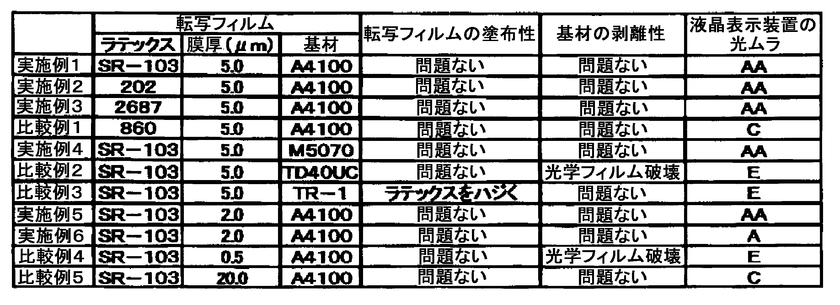
・転写フィルムの塗布性評価
光学フィルムが均一であり、見た目に故障が認められない。:問題ない
光学フィルムが不均一であり、基材上にラテックス層がない部分が認められる。:ラテックスをハジく
偏光板の品質に問題ないがないのは、「問題ない」評価である。
・基材の剥離性評価
基材剥離後の偏光板において、光学フィルムに欠陥が認められない。:問題ない
基材剥離後の偏光板において、光学フィルムに割れが認められる。:光学フィルム破壊
偏光板の品質に問題ないがないのは、「問題ない」評価である。
本出願は、2016年2月5日出願の日本特許出願(特願2016-020819)、及び2016年12月22日出願の日本特許出願(特願2016-250145)に基づくものであり、その内容はここに参照として取り込まれる。
Claims (3)
- 基材上にラテックス層を形成し、乾燥することにより、前記基材上に光学フィルムを形成した転写フィルムを作成する工程、
前記転写フィルムの前記光学フィルム側表面に偏光子を貼り合わせる工程、
前記転写フィルムから前記基材を剥離する工程を有し、
前記ラテックス層を形成するラテックスが、シクロヘキサノンに10重量パーセントで混合された場合、実質的に溶解せず、
前記基材の前記ラテックス層を形成する側の表面エネルギーが、41.0~48.0mN/mであり、
前記光学フィルムの厚さが1~10μmである、偏光板の製造方法。 - 前記偏光子の光学フィルムの反対側に保護フィルムを有する、請求項1に記載の偏光板の製造方法。
- 前記偏光子がポリビニルアルコール系樹脂からなる、請求項1又は2に記載の偏光板の製造方法。
Priority Applications (2)
| Application Number | Priority Date | Filing Date | Title |
|---|---|---|---|
| CN201780009259.4A CN108603967B (zh) | 2016-02-05 | 2017-02-02 | 偏振片的制造方法 |
| KR1020187021347A KR102101687B1 (ko) | 2016-02-05 | 2017-02-02 | 편광판의 제조 방법 |
Applications Claiming Priority (4)
| Application Number | Priority Date | Filing Date | Title |
|---|---|---|---|
| JP2016020819 | 2016-02-05 | ||
| JP2016-020819 | 2016-02-05 | ||
| JP2016250145A JP6637879B2 (ja) | 2016-02-05 | 2016-12-22 | 偏光板の製造方法 |
| JP2016-250145 | 2016-12-22 |
Publications (1)
| Publication Number | Publication Date |
|---|---|
| WO2017135378A1 true WO2017135378A1 (ja) | 2017-08-10 |
Family
ID=59499860
Family Applications (1)
| Application Number | Title | Priority Date | Filing Date |
|---|---|---|---|
| PCT/JP2017/003815 Ceased WO2017135378A1 (ja) | 2016-02-05 | 2017-02-02 | 偏光板の製造方法 |
Country Status (1)
| Country | Link |
|---|---|
| WO (1) | WO2017135378A1 (ja) |
Citations (3)
| Publication number | Priority date | Publication date | Assignee | Title |
|---|---|---|---|---|
| US20040008298A1 (en) * | 2000-08-22 | 2004-01-15 | The Hong Kong University Of Science And Technology | Photo-patterned light polarizing films |
| JP2008529077A (ja) * | 2005-02-01 | 2008-07-31 | エシロール アテルナジオナール カンパニー ジェネラーレ デ オプティック | レンズ基材の表面上に塗膜を貼付ける処理方法 |
| JP2015096579A (ja) * | 2013-11-15 | 2015-05-21 | 日東電工株式会社 | 光学フィルム用水分散型粘着剤組成物、粘着剤層、粘着型光学フィルム、及び、画像表示装置 |
-
2017
- 2017-02-02 WO PCT/JP2017/003815 patent/WO2017135378A1/ja not_active Ceased
Patent Citations (3)
| Publication number | Priority date | Publication date | Assignee | Title |
|---|---|---|---|---|
| US20040008298A1 (en) * | 2000-08-22 | 2004-01-15 | The Hong Kong University Of Science And Technology | Photo-patterned light polarizing films |
| JP2008529077A (ja) * | 2005-02-01 | 2008-07-31 | エシロール アテルナジオナール カンパニー ジェネラーレ デ オプティック | レンズ基材の表面上に塗膜を貼付ける処理方法 |
| JP2015096579A (ja) * | 2013-11-15 | 2015-05-21 | 日東電工株式会社 | 光学フィルム用水分散型粘着剤組成物、粘着剤層、粘着型光学フィルム、及び、画像表示装置 |
Similar Documents
| Publication | Publication Date | Title |
|---|---|---|
| TWI389948B (zh) | 纖維素酯薄膜,偏光板及液晶顯示裝置 | |
| TWI443389B (zh) | 偏光板之製造方法 | |
| CN104040386A (zh) | 碘系偏振片、偏振板、光学膜及图像显示装置 | |
| TW200831571A (en) | Manufacturing method of cellulose acylate film, cellulose acylate film, polarizing plate and liquid crystal display | |
| JP6677722B2 (ja) | 水平配向型液晶表示装置 | |
| JP5965745B2 (ja) | 光学等方性偏光膜保護フィルム及び偏光板 | |
| KR20180099759A (ko) | 적층체 및 액정 표시 장치 | |
| JPWO2015141340A1 (ja) | 偏光板保護フィルム、その製造方法、偏光板及び液晶表示装置 | |
| KR20110126921A (ko) | 편광판 및 표시 장치 | |
| JPWO2015159645A1 (ja) | 偏光板及び液晶表示装置 | |
| CN105122097B (zh) | 偏光板及包含所述偏光板的液晶显示装置 | |
| WO2021085000A1 (ja) | 光学積層体及び表示装置 | |
| JP6655528B2 (ja) | 偏光板および液晶表示装置 | |
| JPWO2015128995A1 (ja) | 偏光板保護フィルム、その製造方法、偏光板及び液晶表示装置 | |
| JP6637879B2 (ja) | 偏光板の製造方法 | |
| JP6007874B2 (ja) | 偏光板保護フィルムとその製造方法、偏光板および液晶表示装置 | |
| JPWO2014068802A1 (ja) | 光学フィルムおよび光学フィルムの製造方法、偏光板および液晶表示装置 | |
| TW201712376A (zh) | 曲面圖像顯示面板用偏光板 | |
| WO2017135378A1 (ja) | 偏光板の製造方法 | |
| WO2021149359A1 (ja) | 光学積層体及び表示装置 | |
| JP6488242B2 (ja) | 複層フィルムの積層物 | |
| JP5555117B2 (ja) | 光学フィルムとその製造方法、偏光板および液晶表示装置 | |
| TWI556001B (zh) | An optical film, a polarizing plate, and an image display device | |
| TWI803771B (zh) | 偏光板疊層以及包括其的顯示裝置 | |
| CN104395422B (zh) | 自由基可固化粘合剂组合物和包括所述自由基可固化粘合剂组合物的偏光板 |
Legal Events
| Date | Code | Title | Description |
|---|---|---|---|
| 121 | Ep: the epo has been informed by wipo that ep was designated in this application |
Ref document number: 17747529 Country of ref document: EP Kind code of ref document: A1 |
|
| ENP | Entry into the national phase |
Ref document number: 20187021347 Country of ref document: KR Kind code of ref document: A |
|
| WWE | Wipo information: entry into national phase |
Ref document number: 1020187021347 Country of ref document: KR |
|
| NENP | Non-entry into the national phase |
Ref country code: DE |
|
| 122 | Ep: pct application non-entry in european phase |
Ref document number: 17747529 Country of ref document: EP Kind code of ref document: A1 |