WO2017135142A1 - 放熱基板、デバイス及び放熱基板の製造方法 - Google Patents
放熱基板、デバイス及び放熱基板の製造方法 Download PDFInfo
- Publication number
- WO2017135142A1 WO2017135142A1 PCT/JP2017/002684 JP2017002684W WO2017135142A1 WO 2017135142 A1 WO2017135142 A1 WO 2017135142A1 JP 2017002684 W JP2017002684 W JP 2017002684W WO 2017135142 A1 WO2017135142 A1 WO 2017135142A1
- Authority
- WO
- WIPO (PCT)
- Prior art keywords
- conductive filler
- inorganic layer
- heat
- binder
- heat dissipation
- Prior art date
- Legal status (The legal status is an assumption and is not a legal conclusion. Google has not performed a legal analysis and makes no representation as to the accuracy of the status listed.)
- Ceased
Links
Images


Classifications
-
- H—ELECTRICITY
- H05—ELECTRIC TECHNIQUES NOT OTHERWISE PROVIDED FOR
- H05K—PRINTED CIRCUITS; CASINGS OR CONSTRUCTIONAL DETAILS OF ELECTRIC APPARATUS; MANUFACTURE OF ASSEMBLAGES OF ELECTRICAL COMPONENTS
- H05K7/00—Constructional details common to different types of electric apparatus
- H05K7/20—Modifications to facilitate cooling, ventilating, or heating
-
- H—ELECTRICITY
- H10—SEMICONDUCTOR DEVICES; ELECTRIC SOLID-STATE DEVICES NOT OTHERWISE PROVIDED FOR
- H10W—GENERIC PACKAGES, INTERCONNECTIONS, CONNECTORS OR OTHER CONSTRUCTIONAL DETAILS OF DEVICES COVERED BY CLASS H10
- H10W40/00—Arrangements for thermal protection or thermal control
- H10W40/20—Arrangements for cooling
- H10W40/25—Arrangements for cooling characterised by their materials
Definitions
- the present invention relates to a heat dissipation substrate, a device, and a manufacturing method of the heat dissipation substrate.
- an aluminum substrate having such an insulating film is commercially available.
- This insulating film uses resin as a base material.
- resin epoxy, polyimide, or the like is used.
- the thermal conductivity of these resins is generally about 0.1 W / mK.
- silica, alumina, silicon nitride, boron nitride or the like is used as the high thermal conductive filler.
- the thermal conductivity of silica is about 1 W / mK
- alumina is about 25 W / mK. Since silica is inexpensive, it is very often used as a heat conductive packaging material for electronic components.
- Alumina has a higher thermal conductivity than silica, but is more expensive than silica.
- Silicon nitride and boron nitride have higher thermal conductivity, but their use is limited because they are very expensive.
- heat dissipation board examples include, for example, a circuit board in which a mixture of a bisphenol A type epoxy resin and an inorganic filler is laminated on a metal base (see Japanese Patent Laid-Open No. 6-44824), an inorganic hollow powder. And a metal base circuit board for LEDs formed by laminating an epoxy resin or the like containing a metal base material (see Japanese Patent Application Laid-Open No. 2009-129801) and the like.
- the present invention has been made based on the above-described circumstances, and provides a heat dissipation substrate excellent in heat resistance, durability against ultraviolet rays, and manufacturability, a device including the heat dissipation substrate, and a method of manufacturing the heat dissipation substrate. With the goal.
- the invention made to solve the above problems is a heat dissipation board comprising a base material mainly composed of a metal and a heat conductive layer laminated on one surface of the base material and having an insulating property
- the heat conductive layer includes a heat conductive filler, a binder mainly composed of phosphate glass, which is bonded to the heat conductive filler, and a silica-based compound existing in a gap between the heat conductive filler and the binder.
- a ratio of the total volume of the thermally conductive filler and binder to the total volume of the thermally conductive filler, binder and silica-based compound in the inorganic layer is 55% or more and 84%.
- the ratio of the volume of the thermally conductive filler to the total volume of the thermally conductive filler and the binder is 40% or more and 99% or less.
- the inorganic layer included in the heat conductive layer includes phosphate glass instead of resin as a binder, and further includes a silica-based compound that exists in the gap between the heat conductive filler and the inorganic binder.
- the heat resistance of a heat conductive layer and the durability to an ultraviolet-ray are improved significantly.
- the content of the heat conductive filler in the inorganic layer is in the above range, and the heat conductive filler and the binder are uniformly dispersed by the presence of the silica-based compound. Also excellent.
- the main component metal of the base material is aluminum, aluminum alloy, copper, copper alloy or a combination thereof
- the thermally conductive filler is aluminum oxide, magnesium oxide, aluminum nitride, silicon nitride, crystalline silicon oxide, Quartz, boron nitride, diamond, or a combination thereof may be a main component.
- a median diameter of a heat conductive filler 6 micrometers or more and 100 micrometers or less are preferable.
- the average thickness of the inorganic layer is preferably 30 ⁇ m or more and 300 ⁇ m or less. By setting the average thickness of the inorganic layer in the above range, both insulation and thermal conductivity can be achieved.
- Another invention made in order to solve the above-mentioned problems is a device provided with the above-mentioned heat dissipation board.
- the device is excellent in heat dissipation because it includes the heat dissipation substrate.
- Still another invention made in order to solve the above-mentioned problems is the manufacture of a heat dissipation board comprising a base material mainly composed of a metal and a thermally conductive layer laminated on one surface of the base material and having an insulating property.
- a method of applying a composition for an inorganic layer containing a thermally conductive filler and binder particles mainly composed of phosphate glass on one surface of the substrate, followed by drying, and the inorganic material A step of heating a coating composition containing a siloxane compound or polysilazane on one side of the coating film of the layer composition, and applying the coating composition and heating the coating composition,
- the ratio of the total volume of the thermal conductive filler and binder to the total volume of the thermal conductive filler, binder particles, and silica-based compound is 55% to 84%, and the thermal conductivity Ratio of the volume of the heat conductive filler to the total volume of the filler and the binder is equal to or less than 99% 40%.
- the manufacturing method of the heat dissipation substrate uses phosphate glass instead of resin as binder particles, and impregnates the coating film of the inorganic layer composition containing the heat conductive filler and the binder with a siloxane compound by coating,
- An inorganic layer containing a silica-based compound can be formed in the gap between the heat conductive filler and the inorganic binder by heating.
- the content rate of the heat conductive filler in the coating film formed is the said range, and also a heat conductive filler and a binder disperse
- the heat dissipation board to be used is excellent in heat dissipation and manufacturability.
- the coating of the inorganic layer composition may be performed by spraying or printing.
- the drying temperature of the inorganic layer composition is preferably 100 ° C. or lower, and the heating temperature of the coating composition is preferably 150 ° C. or higher and 300 ° C. or lower.
- a step of baking the coating film at a temperature in such a range the adhesion strength between the base material and the inorganic layer and between the thermal conductive filler, the inorganic binder, and the silica-based compound can be increased.
- main component means the most abundant component (for example, 50% by mass or more) on a mass basis.
- median diameter means a particle diameter at which the volume integrated value is 50% in the particle size distribution obtained by observing a micrograph taken after smooth polishing of the cross section of the layer.
- the heat dissipation substrate and device of the present invention are excellent in heat resistance, durability to ultraviolet rays, and manufacturability.
- substrate of this invention can obtain the thermal radiation board excellent in heat resistance, durability to an ultraviolet-ray, and manufacturability.
- the said heat dissipation board is mainly provided with the base material and the heat conductive layer laminated
- the base material is a plate-like member having a metal as a main component and having a heat conductive layer laminated on one surface.
- the main component metal of the base material aluminum, aluminum alloy, copper, copper alloy or a combination thereof is preferable from the viewpoint of cost and thermal conductivity.
- aluminum or an aluminum alloy is more preferable from the viewpoint of weight reduction and cost.
- the thermal conductivity of aluminum is about 200 to 250 W / mK
- the thermal conductivity of copper is about 350 to 400 W / mK
- the heat conductivity is superior to the thermal conductivity of iron (about 80 W / mK). .
- the main component of the base material is an aluminum alloy, specifically, an aluminum alloy in the 3000s, 5000s, or 6000s specified in JIS-H4000 (2014) is preferable.
- the lower limit of the average thickness of the substrate is preferably 0.1 mm, and more preferably 0.5 mm.
- the upper limit of the average thickness is preferably 5 mm, and more preferably 4 mm.
- the average thickness is smaller than the lower limit, the strength of the heat dissipation substrate may be reduced.
- the average thickness exceeds the upper limit, it may be difficult to use the heat dissipation board in a downsized electronic device.
- a heat conductive layer is mainly provided with the inorganic substance layer laminated
- the heat conductive layer may further include a coating layer laminated on one surface of the inorganic layer.
- the heat conductive layer may be laminated on only one surface of the base material or may be laminated on both surfaces, but is preferably laminated only on one surface.
- a metal is superior in thermal conductivity to phosphate glass, which is a binder of a heat conductive layer. Therefore, the surface of the heat radiating substrate on which the heat conductive layer is not laminated is brought into contact with a coolant, thereby the heat radiating substrate. The heat dissipation efficiency is improved.
- the inorganic layer is a layer that is directly laminated on one surface of the base material, and includes a thermally conductive filler, a binder mainly composed of phosphate glass that binds the thermally conductive filler, and the thermal conductivity. And a silica-based compound present in the gap between the conductive filler and the binder. This inorganic layer can provide insulation to the heat dissipation substrate.
- the lower limit of the average thickness of the inorganic layer is preferably 10 ⁇ m, more preferably 30 ⁇ m, and even more preferably 50 ⁇ m.
- the upper limit of the average thickness is preferably 300 ⁇ m, more preferably 200 ⁇ m, and even more preferably 150 ⁇ m.
- the average thickness is smaller than the lower limit, defects such as pinholes in the inorganic layer are likely to occur, and the insulating properties of the inorganic layer may be reduced.
- the average thickness exceeds the upper limit, the thermal resistance of the inorganic layer increases, and the heat dissipation property of the heat dissipation substrate may be reduced.
- the thermally conductive filler is dispersed in the inorganic layer to improve the thermal conductivity in the inorganic layer. If each particle of the thermally conductive filler is dispersed in the inorganic layer without coming into contact with other particles, the thermal conductivity of the inorganic layer may be difficult to improve.
- the particles are preferably in contact with each other.
- thermally conductive filler aluminum oxide, magnesium oxide, aluminum nitride, silicon nitride, crystalline silicon oxide, quartz (crystalline silicon), boron nitride, diamond, zinc oxide, cerium oxide, beryllium oxide, etc.
- aluminum oxide, magnesium oxide, aluminum nitride, silicon nitride, crystalline silicon oxide, quartz, boron nitride, diamond and combinations thereof are preferable, and aluminum oxide is more preferable.
- the thermal conductivity of the thermal conductive filler those having higher heat conductivity than the binder are preferable.
- the thermal conductivity of the thermal conductive filler is equal to or lower than that of the binder, the thermal conductivity of the inorganic layer is not improved even if the thermal conductive filler is added.
- the thermal conductivity of crystalline silicon oxide is about 1.0 W / mK
- the thermal conductivity of crystalline silicon (quartz) is about 10 W / mK.
- Aluminum oxide (crystalline) has a thermal conductivity of about 20 to 35 W / mK, and is suitable as a thermally conductive filler because of its relatively low price.
- Diamond is considered to have a thermal conductivity of 1000 W / mK or more, but is very expensive.
- the lower limit of the median diameter of the heat conductive filler is preferably 6 ⁇ m, and more preferably 10 ⁇ m.
- the upper limit of the median diameter is preferably 100 ⁇ m, more preferably 50 ⁇ m, and even more preferably 30 ⁇ m.
- the median diameter is smaller than the lower limit, the particles of the heat conductive filler are difficult to contact with each other and the interface with the binder is increased, which may make it difficult to improve the heat conductivity of the inorganic layer.
- the median diameter exceeds the upper limit, it may be difficult to form the inorganic layer by a coating method described later, or the inorganic layer may become excessively thick.
- the ratio of the median diameter of the heat conductive filler to the average thickness of the inorganic layer is preferably 0.2 times or more and 0.5 times or less.
- the ratio is smaller than the lower limit, the interface of the thermally conductive filler increases, and as a result, the thermal conductivity may decrease.
- the ratio exceeds the upper limit, the surface roughness of the inorganic layer may be increased, and the thickness of the inorganic layer may not be controlled.
- the lower limit of the content ratio of the thermally conductive filler to the total of the thermally conductive filler and the binder in the inorganic layer of the thermally conductive filler is 40% by volume, preferably 45% by volume, and 50% by volume. More preferred.
- the upper limit of the content ratio is 99% by volume, preferably 95% by volume, and more preferably 85% by volume.
- the content ratio exceeds the upper limit, the amount of the binder is decreased, whereby the adhesive strength between the base material and the inorganic layer is lowered, and the inorganic layer may be peeled off.
- binder The binder binds the heat conductive filler and contains phosphate glass as a main component. This binder has a function of bonding the substrate and the inorganic layer.
- boric acid (B 2 O 3 ), vanadate (V 2 O 5 ), etc. are used alone, or Li, Na, K oxide, P 2 O 5 , Al 2 O 3 , SiO You may add what mixed 2 a suitable quantity.
- This phosphate glass preferably has a lower melting point than the metal that is the main component of the substrate.
- an inorganic substance layer can be easily formed by the method mentioned later because the melting point of phosphate glass is lower than the melting point of the metal.
- the melting point of aluminum is about 660 ° C.
- the melting point of phosphate glass is preferably 430 ° C. or higher and 650 ° C. or lower.
- this phosphate glass generally has higher thermal conductivity than epoxy resin and the like. For this reason, the inorganic layer is excellent in heat dissipation efficiency as compared with the resin layer of the conventional heat dissipation substrate.
- the thermal conductivity of a general resin is about 0.1 W / mK
- the thermal conductivity of phosphate glass is about 1.0 W / mK.
- the softening temperature of phosphate glass is about 400 ° C
- the heat resistance temperature of general resins is about 200 ° C, so the heat resistance is greatly improved by using phosphate glass as a binder. To do.
- the lower limit of the content ratio of the total of the thermal conductive filler and binder in the inorganic layer to the total of the thermal conductive filler, binder and silica compound is 55% by volume, and preferably 60% by volume.
- the upper limit of the content ratio is 84% by volume, preferably 80% by volume, and more preferably 75% by volume.
- the silica-based compound exists in the gap between the thermally conductive filler and the binder.
- the silica-based compound means a compound containing silicon and oxygen, and may contain other elements such as nitrogen.
- the silica compound amorphous silicon oxide is preferable.
- the silicon oxide is preferably derived from polysiloxane such as alkoxysiloxane having a siloxane skeleton or alkoxysiloxane oligomer, polysilazane, or a combination thereof.
- the lower limit of the content of the silica-based compound in the inorganic layer is preferably 15% by volume, more preferably 20% by volume, and even more preferably 25% by volume.
- an upper limit of content of a silica type compound 45 volume% is preferable and 40 volume% is more preferable.
- the content of the silica-based compound is smaller than the above lower limit, the dispersibility of the heat conductive filler and the binder may be lowered. Conversely, if the content of the silica-based compound exceeds the above upper limit, the thermal conductivity or moldability of the inorganic layer may be reduced.
- a conventional resin-based coating film has a weak bond between organic materials in the resin, and the organic bond portion is decomposed by ultraviolet rays.
- the inorganic layer of the present invention contains SiO 2, further by a binder mainly composed of phosphate glass, stronger bond compared to the organic material, not decomposed by ultraviolet rays.
- the coating layer is laminated on one surface of the inorganic layer.
- a coating layer contains the silica type compound contained in an inorganic substance layer as a main component. That is, the coating layer is a layer formed of a silica-based compound that has not been impregnated into the inorganic layer.
- the phosphate glass which is the main component of the binder in the inorganic layer, is slightly inferior in water resistance, and there is a possibility that an alkali component flows out from the phosphate glass, but the coating layer covers the inorganic layer, The outflow of this alkali component can be suppressed.
- the lower limit of the average thickness of the coating layer is preferably 0.5 ⁇ m, more preferably 5 ⁇ m, and even more preferably 10 ⁇ m.
- the upper limit of the average thickness is preferably 50 ⁇ m, more preferably 40 ⁇ m, still more preferably 35 ⁇ m, and particularly preferably 30 ⁇ m.
- the coating layer functions as a heat insulating layer, and there is a possibility that the heat dissipation property of the heat dissipation substrate is lowered, or that the coating layer is cracked.
- the device includes the heat dissipation substrate. Specifically, a heating element such as an electronic device is disposed on the inorganic layer side of the heat dissipation substrate, and a coolant is disposed on the base material side of the heat dissipation substrate. Examples of the coolant include a water-cooling device, an air-cooling device, and a heat conduction member such as a cooling fin.
- the inorganic layer included in the heat conductive layer includes phosphate glass instead of resin as a binder, and further includes a silica-based compound that exists in a gap between the heat conductive filler and the inorganic binder.
- the heat resistance of a heat conductive layer and the durability to an ultraviolet-ray are improved significantly.
- the content of the heat conductive filler in the inorganic layer is in the above range, and the heat conductive filler and the binder are uniformly dispersed by the presence of the silica-based compound. Also excellent.
- the device since the device includes the heat dissipation substrate, the device is excellent in heat resistance, durability to ultraviolet rays, and manufacturability.
- the method for manufacturing a heat dissipation substrate is a method for manufacturing a heat dissipation substrate including a base material containing a metal as a main component and a heat conductive layer laminated on one surface of the base material and having an insulating property.
- the manufacturing method of the said heat dissipation board is dried after coating the composition for inorganic layers containing the heat conductive filler and the binder particle
- the manufacturing method further includes a third step of firing the coating film of the inorganic layer composition after the coating composition is heated.
- the inorganic layer composition is applied and dried on one surface of the substrate to form a coating film of the inorganic layer composition.
- This composition for inorganic layers contains a thermally conductive filler and binder particles mainly composed of phosphate glass.
- a step of preparing binder particles by pulverization of phosphate glass binder particle preparation step
- a step of preparing a composition for inorganic layer containing the binder particles composition step for inorganic layer composition
- a step of coating the inorganic layer composition coating step
- drying step drying the coated inorganic layer composition
- Binder particle preparation process for example, a phosphate glass is pulverized to a desired size using a pulverizer such as a pot mill or a jet mill to obtain binder particles.
- the lower limit of the median diameter of the binder particles is preferably 1 ⁇ m, more preferably 2.5 ⁇ m, and particularly preferably 5 ⁇ m.
- the upper limit of the median diameter is preferably 100 ⁇ m, more preferably 80 ⁇ m, and further preferably 50 ⁇ m.
- the median diameter is smaller than the lower limit, the binder particles tend to aggregate and the uniformity of the inorganic layer may be reduced.
- the median diameter exceeds the upper limit, the binder particles and the heat conductive filler are not sufficiently mixed, and the uniformity of the inorganic layer may be lowered.
- the inorganic particle layer composition is prepared by mixing the binder particles, the thermally conductive filler, and water or an aqueous solvent.
- the content ratio of the thermally conductive filler to the total of the thermally conductive filler and the binder particles in the inorganic layer composition is based on the total of the thermally conductive filler and the binder of the thermally conductive filler described in the inorganic layer of the heat dissipation substrate. This is the same as the range of the content ratio.
- aqueous solvent examples include linear or branched aliphatic lower alcohols such as methanol, ethanol, n-propanol, 2-propanol, and t-butyl alcohol; aromatic alcohols such as benzyl alcohol and 2-phenylethanol; Polyethylene glycol such as propylene glycol, ethylene glycol, diethylene glycol, triethylene glycol, tetraethylene glycol, PEG200, PEG400; polypropylene glycol such as dipropylene glycol, tripropylene glycol; 1,3-butanediol, 2,3-butanediol, Polyhydric alcohols such as 1,4-butanediol, 1,5-pentanediol, hexylene glycol; ethylene glycol monomethyl ether, ethylene glycol mono Chill ether, ethylene glycol dimethyl ether, ethylene glycol diethyl ether, 3-methyl-3-methoxybutanol, diethylene glycol monomethyl ether, dimethyl
- the lower limit of the solid content concentration of the inorganic layer composition is preferably 40% by mass, more preferably 50% by mass.
- the upper limit of the solid content concentration is preferably 70% by mass, and more preferably 65% by mass. If the solid content concentration is smaller than the lower limit, the thickness of the inorganic layer is greatly reduced by baking after coating, and it may be difficult to obtain an inorganic layer having a desired thickness, and it takes time to dry the heat dissipation. There is a possibility that the manufacturing efficiency of the substrate is lowered. Conversely, when the solid content concentration exceeds the upper limit, it may be difficult to uniformly apply the inorganic layer composition.
- the inorganic layer composition is applied to one surface of the substrate to form a coating film.
- the coating method include coater coating, spray coating, and printing coating. Among these, spray coating and printing coating are preferable from the viewpoint that the inorganic layer composition can be easily and uniformly applied.
- drying process In the drying step, after coating the inorganic layer composition to form a coating film, the coating film is dried and the solvent is removed.
- the drying temperature 15 ° C is preferred and 20 ° C is more preferred.
- the upper limit of the drying temperature is preferably 100 ° C, more preferably 90 ° C.
- the drying temperature is smaller than the said minimum, drying requires time and there exists a possibility that the manufacturing efficiency of the said heat sink may fall.
- the drying temperature exceeds the upper limit, water or an aqueous solvent may suddenly boil and there may be bubbles in the coating film, which may make it difficult to form a uniform inorganic layer.
- the lower limit of the drying time is preferably 10 minutes, and more preferably 30 minutes.
- the upper limit of the drying time is preferably 600 minutes, and more preferably 300 minutes.
- the thermally conductive filler and the binder particles are formed between the thermally conductive filler and the binder particles. Since the packing ratio of ideal spherical material close-packing (hexagonal close-packing) is 74%, the packing ratio in the state where only a powder having a uniform particle diameter is deposited does not exceed 74%. When the gap defect is contained, the filling rate is reduced to about 50%. In the present invention, since powder having a variation in particle size including a thermally conductive filler having a large particle size and binder particles having a small particle size is used, small particles may be arranged in the gap between the large particles and the large particles.
- the filling rate may exceed 74%, but it is about 85% at the maximum.
- the actual powder filling ratio is about 50 to 70% when formed in a dry state, and 60 to 90 when a film is formed by a spray method from a state where powders having different particle diameters are dispersed in a solution and dried. %. If only the powder having a large average particle size and a small particle size distribution is used, the filling rate approaches 70%, and if only the particles having a small average particle size are used, the filling rate decreases to about 50%.
- the filling ratio can be made close to 90% by increasing the average distribution mainly of particles having a large average particle diameter, and drying after preparing an aqueous solution. Thereby, insulation and heat dissipation can be improved.
- the glass of the binder particles melts and the glasses gather.
- the amount of the thermally conductive filler added is large, for example, when baking is performed at 480 ° C., the viscosity of the glass is lowered and the movement of the molten glass becomes intense, and the glass agglomerated portion and the glass are not present. The gap portion is formed separately. At that time, a portion where the thermally conductive filler is also dragged by the glass and the dispersion state becomes non-uniform appears. Thereby, a large unevenness
- the following second step is performed in order to improve insulation while avoiding aggregation of the thermally conductive filler.
- a coating composition containing a siloxane compound is applied and heated on one surface of the coating film of the inorganic layer composition formed in the first step, and this coating film is impregnated with the siloxane compound.
- This step includes, for example, a step of applying the coating composition to one surface of the coating film of the inorganic layer composition (coating step) and a step of heating the coating composition after coating (heating step). Has mainly.
- the coating composition containing a siloxane compound or polysilazane is impregnated with the siloxane compound by coating on one surface of the coating film of the inorganic layer composition.
- the above siloxane compound is a compound having a siloxane bond, and may have a substituent such as an alkyl group.
- alkoxysiloxane alkoxysiloxane, its oligomer or polysiloxane using it is preferable.
- alkoxysiloxane examples include alkoxysiloxane oligomers such as alkoxydisiloxane, and alkoxy-containing polysiloxanes having a three-dimensional network structure. Among these, alkoxysiloxane oligomers are preferable from the viewpoint of improving the strength of the coating layer.
- the “siloxane oligomer” means a polymer in which about 2 to 100 siloxane monomers are polymerized.
- the coating composition is in a liquid state and usually further contains a solvent.
- the solvent include nonpolar solvents in addition to the above water and aqueous solvents.
- nonpolar solvent examples include chain hydrocarbon solvents such as hexane, heptane, octane and pentane, alicyclic hydrocarbon solvents such as cyclohexane, and aromatic hydrocarbon solvents such as benzene, toluene and xylene. Of these, aromatic hydrocarbon solvents are preferred, and toluene and xylene are more preferred.
- Examples of the method for applying the coating composition to the coating film of the inorganic layer composition include a coating method using a brush, a coater, etc. According to these methods, the siloxane compound can be efficiently filled into the coating film. .
- the siloxane compound coated in the coating step is modified into a silica-based compound by hydrolysis by heating and a heat dealcoholization reaction treatment is performed.
- the siloxane compound becomes a silica material that loses fluidity (silica-based compound), and cannot be moved greatly by being surrounded by the silica material while keeping the thermally conductive filler and binder particles uniformly dispersed. Fixed in state.
- the organic material component weak to ultraviolet rays is removed by this process.
- generated silica type compound is about 1 W / mK, and is equivalent to a glass material.
- the lower limit of the heating temperature is preferably 150 ° C, more preferably 200 ° C.
- an upper limit of heating temperature 300 degreeC is preferable and 260 degreeC is more preferable. If the heating temperature is smaller than the above lower limit, it takes time for heating, and the production efficiency of the heat dissipation substrate may be reduced. On the other hand, when the heating temperature exceeds the above upper limit, the binder particles in the inorganic layer composition may melt, and it may be difficult to form a uniform inorganic layer.
- the lower limit of the heating time is preferably 10 minutes, more preferably 20 minutes.
- the upper limit of the heating time is preferably 100 minutes, and more preferably 50 minutes. If the heating time is less than the above lower limit, the siloxane compound may not be sufficiently modified. On the other hand, when the heating time exceeds the above upper limit, the production efficiency of the heat dissipation substrate may be reduced.
- the content ratio with respect to the sum of the heat conductive filler and the binder particles is the sum of the heat conductive filler and the binder described in the inorganic layer of the heat dissipation substrate with respect to the sum of the heat conductive filler, the binder, and the silica compound.
- the ratio and the range of the content of the heat conductive filler to the total of the heat conductive filler and the binder are the same.
- ⁇ Third step> the coating film is baked after the second step to solidify after the binder particles in the coating film are melted.
- the pore portion in the coating film is reduced, but a minute amount of fine pores accompanying the release of the reactive component remains.
- These very small numbers of pores are often generated as gaps at the interface between the thermally conductive filler, the binder particles, the silica-based compound and the substrate. This gap reduces the adhesion between the components.
- the binder particles soften and flow into these gaps or poorly adhered portions, thereby improving the adhesion of the entire inorganic layer and the adhesion to the substrate.
- the binder particles do not move and agglomerate and contribute only to the improvement of adhesion. Note that this step is not necessarily performed depending on a material to be used and conditions of other steps.
- the lower limit of the firing temperature is preferably 430 ° C, more preferably 450 ° C.
- the upper limit of the firing temperature is preferably 600 ° C and more preferably 550 ° C. If the firing temperature is lower than the lower limit, the binder particles in the coating film may not be sufficiently melted. On the other hand, if the firing temperature exceeds the upper limit, the thermally conductive filler in the coating film may melt, and an inorganic layer having sufficient thermal conductivity may not be formed.
- the lower limit of the firing time is preferably 30 minutes, more preferably 50 minutes.
- the upper limit of the firing time is preferably 120 minutes, and more preferably 100 minutes. If the firing time is smaller than the lower limit, the binder particles in the coating film may not be sufficiently melted. On the other hand, when the firing time exceeds the above upper limit, the production efficiency of the heat dissipation substrate may be reduced.
- the coating composition not impregnated in the inorganic layer forms a coating layer. Further, this coating layer (coating composition) may be peeled off from the inorganic layer.
- the second step and the third step are preferably performed separately, but may be performed simultaneously. That is, in the manufacturing method of the heat dissipation substrate, it is preferable that hydrolysis of the siloxane compound and firing of the coating film (melting and solidification of the binder particles) are performed separately, but they may be performed simultaneously.
- the manufacturing method of the heat dissipation substrate uses phosphate glass instead of resin as binder particles, and impregnates the coating film of the inorganic layer composition containing the heat conductive filler and the binder with a siloxane compound by coating,
- An inorganic layer containing a silica-based compound can be formed in the gap between the heat conductive filler and the inorganic binder by heating.
- the content rate of the heat conductive filler in the coating film formed is the said range, and also a heat conductive filler and a binder disperse
- the heat dissipation board to be used is excellent in heat dissipation and manufacturability.
- substrate is not limited to the said embodiment.
- the heat dissipation substrate may include a plurality of base materials and inorganic layers in the thickness direction.
- the composition of the plurality of base materials and inorganic layers may be different.
- Example 1 An aluminum plate (industrial pure aluminum 1050, average thickness 2 mm) as a substrate was cut into 50 mm length and 50 mm width by a shearing machine, and the surface was washed with a neutral detergent.
- low melting point phosphate glass flakes (“VQ0028” manufactured by Nippon Frit Co., Ltd.) were pulverized with a jet mill so that the median diameter was 10 ⁇ m to obtain binder particles.
- the inorganic binder composition was prepared by mixing and stirring the binder particles, granular aluminum oxide (“AS30” from Showa Denko KK, average particle size 18 ⁇ m) as heat conductive filler, and water.
- the content ratio of the heat conductive filler to the total of the heat conductive filler and the binder particles in the inorganic layer composition was 70% by volume.
- the inorganic layer composition is applied onto the surface of the substrate by spraying for 60 seconds so that the average thickness of the coating after baking is 100 ⁇ m, and then dried. Dry in an oven at 60 ° C.
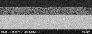
- a cross-sectional photograph of the substrate and the coating film in this state is shown in FIG.
- the average thickness of the coating film (inorganic layer) was measured using an eddy current film thickness meter (“MMS 3AM” manufactured by Fisher Instrument Co., Ltd.).
- a coating composition containing a siloxane compound (“KR255” from Shin-Etsu Chemical Co., Ltd.) was applied to the surface of the coating film with a brush, and the excess solution on the surface was peeled off with a squeegee, and then in the atmosphere for 2 hours. Left to stand. Thereafter, heat treatment was performed at 250 ° C. for 30 minutes in an electric furnace, and further, baking was performed at 480 ° C. for 60 minutes to form an inorganic layer.
- a siloxane compound (“KR255” from Shin-Etsu Chemical Co., Ltd.
- the total content of the heat conductive filler and the binder in the inorganic layer is 80% by volume with respect to the total of the heat conductive filler, the binder, and the silica compound, and the heat conductive filler is based on the total of the heat conductive filler and the binder.
- the content ratio was 70% by volume.
- Example 1 In the same procedure as in Example 1, the inorganic layer composition was applied to a substrate by a spray method and dried at 60 ° C. in a drying furnace to form a coating film. After drying, the coating film was baked at 480 ° C. for 60 minutes, and then a coating composition containing a siloxane compound was applied to the coating film, followed by heat treatment at 250 ° C. for 30 minutes. A cross-sectional photograph of the obtained heat dissipation substrate is shown in FIG. In the heat dissipation substrate of Comparative Example 1, no silica-based compound exists in the gap between the thermally conductive filler and the binder. As a result, in Comparative Example 1, as shown in FIG. 3, large irregularities were formed on the surface of the inorganic layer, and the film could not be formed uniformly.
- Examples 2 to 4 and Comparative Examples 2 to 5 The content ratio of the total heat conductive filler and binder in the inorganic layer to the total of the heat conductive filler, binder and silica compound, and the content ratio of the heat conductive filler to the total of the heat conductive filler and the binder are shown. Except that the value described in 1 was used, the heat dissipation substrates of Examples 2 to 4 and Comparative Examples 2 to 5 were obtained in the same manner as Example 1.
- the thermal resistance of the heat dissipation board was measured and evaluated by the following procedure. First, an aluminum block having a side of 100 mm was prepared and immersed in water that was circulated so as to maintain 18 ° C. to a depth of 75 mm. Next, heat conduction grease (“G747” from Shin-Etsu Chemical Co., Ltd., heat conductivity 0.9 W / mK) is applied to the base material side surface of the heat dissipation substrate so that the average thickness is 0.08 mm. The heat dissipation substrate was attached to the upper surface of the aluminum block that was not submerged.
- heat conduction grease (“G747” from Shin-Etsu Chemical Co., Ltd., heat conductivity 0.9 W / mK)
- the heat conductive grease is pasted on the surface of the inorganic layer of the heat dissipation substrate so as to have an average thickness of 0.08 mm, and the heat transfer grease and the heat dissipation substrate and the heater (AIN ceramic heater with thermocouple of Sakaguchi Electric Heat Company, 25 mm long, 25 mm wide, and 2.5 mm high).
- a load of 5 N was applied from the heater side to the laminate of the heater, the heat dissipation substrate and the aluminum block to fix the components together, and a thermocouple was attached to the aluminum block to obtain a laminate with a heat dissipation substrate.
- the heater was heated by energizing the heater of the laminate with the heat dissipation substrate.
- the temperature inside the heater reaches 50 ° C
- the aluminum block surface temperature A (° C)
- the heater internal temperature H (° C)
- the heater output P (W)
- Resistance R (° C./W) was calculated.
- R (HA) / P (1)
- the thermal resistance R (m 2 K / W) per unit area is obtained by multiplying the obtained thermal resistance R by the area of the heater (2.5 mm square) so that the thermal resistance per unit area can be evaluated. Calculated. Since the thermal resistance of the thermal conductive grease is added to the thermal resistance r, the thermal resistance of the thermal conductive grease (0.00008 (m) /0.98 (W / mK)) is subtracted from the thermal resistance r. The thermal resistance value of the heat dissipation substrate was calculated.
- the thermal resistance of an aluminum plate having a thickness of 2 mm and a thermal conductivity of 200 W / mK is 0.1 cm 2 W / K
- the thermal resistance of sapphire ( ⁇ alumina) having a thickness of 1 mm and a thermal conductivity of 25 W / mK is 0. .4 cm 2 W / K. Therefore, the inorganic layer having a thermal resistance of 0.2 cm 2 W / K or less is good (A)
- the layer having a thermal resistance of 0.2 cm 2 W / K to 0.4 cm 2 W / K or less is acceptable (B), otherwise Was evaluated as defective (C).
- the + terminal (15 mm diameter stainless steel ball electrode) was connected to the inorganic layer side, and the-terminal was connected to the substrate side. Thereafter, a DC voltage was gradually applied, and the voltage at the time when a current of 1 mA or more flowed was measured at each of five arbitrary points on the heat dissipation board, and the lowest value among them was defined as the minimum insulation withstand voltage.
- the heat resistance against soldering was evaluated. Specifically, a soldering iron (“X1000” manufactured by Taiyo Electric Industry Co., Ltd.) is heated to 300 ° C. and pressed against the inorganic layer of the heat dissipation substrate for 1 minute to determine whether the inorganic layer is melted or discolored. Examined. In this example and the comparative example, none of the heat dissipation substrates was melted or discolored, and the heat resistance was good (A).
- a material that could form an inorganic layer and that did not peel from the substrate was designated as A.
- B1 represents that the inorganic layer was peeled from the substrate as described above, and B2 represents that the inorganic layer could not be formed.
- thermo conductive filler content ratio is (thermal conductive filler) / (thermal conductive filler + binder)
- total content ratio of thermal conductive filler and binder is (thermal conductive filler + Binder) / (thermally conductive filler + binder + silica compound).
- the heat dissipation substrates of Examples 1 to 4 were excellent in thermal conductivity, insulation and heat resistance, and no irregularities were observed in appearance.
- the heat dissipation board of Comparative Examples 2 and 4 that could be evaluated was excellent in insulation and heat resistance, the thermal conductivity was insufficient. This is probably because the content of the heat conductive filler was too small.
- Example 2 in which the contents of the thermally conductive filler and the silica-based compound are large has a smaller thermal resistance than Example 1. This is considered to be due to the dispersion effect of the thermally conductive filler and binder by the silica-based compound.
- the overall thermal resistance is determined by (1) the high thermal conductivity effect of the thermally conductive filler, (2) the content of the binder and the silica-based compound, and (3) the total inhibition by the gap, so the amount of thermally conductive filler is large,
- the thermal resistance of the heat dissipation substrate of Example 2 in which the proportion of the silica-based compound is large and the gap filling amount is large is smaller.
- the heat dissipation substrate and device of the present invention are excellent in heat resistance, durability to ultraviolet rays, and manufacturability.
- substrate of this invention can obtain the thermal radiation board excellent in heat resistance, durability to an ultraviolet-ray, and manufacturability.
- These heat radiating substrates and devices can be suitably used for electronic components that are increasing in power, increased in power density, and the like.
Landscapes
- Physics & Mathematics (AREA)
- Thermal Sciences (AREA)
- Engineering & Computer Science (AREA)
- Microelectronics & Electronic Packaging (AREA)
- Cooling Or The Like Of Semiconductors Or Solid State Devices (AREA)
- Insulated Metal Substrates For Printed Circuits (AREA)
- Cooling Or The Like Of Electrical Apparatus (AREA)
- Laminated Bodies (AREA)
Abstract
本発明の放熱基板は、金属を主成分とする基材と、この基材の一方の面に積層された熱伝導層とを備え、熱伝導層は、熱伝導性フィラーと、リン酸塩ガラスを主成分とするバインダーと、シリカ系化合物とを含有する無機物層とを有する。無機物層における熱伝導性フィラーとバインダーとの合計割合、並びに熱伝導性フィラーの割合が、それぞれ特定範囲である。
Description
本発明は、放熱基板、デバイス及び放熱基板の製造方法に関する。
高発熱電子部品に用いられる絶縁放熱基板には、放熱性のほかに、絶縁性、耐熱性、耐久性などが要求される。近年、電子部品の高電力化、高電力密度化等に伴い、電子部品から発生する熱量が大きくなっている。例えば高輝度発光ダイオード(LED)、高発熱集積回路(IC)、絶縁ゲートバイポーラトランジスタ(IGBT)のような電子部材やレーザー発振装置では、熱伝導に優れた冷却部材や冷却基材への接合による放熱が求められる。特にLEDなどでは金属基板に絶縁樹脂を塗布したメタル基板が使われる。
このようなメタル基板においてアルミニウム板上に良好な熱伝導性と絶縁性とを併せ持つ皮膜を形成させる方法として、皮膜の母材材料に高熱伝導性のフィラーを添加する方法が提案されている。熱伝導の良好な皮膜を形成するには、皮膜の母材材料の熱伝導性が良好であること、高熱伝導性フィラーの熱伝導率が高いこと、及び高熱伝導性フィラーの構成割合が多いことが必要である。また、このような高熱伝導性フィラー含有皮膜の膜厚が大きいと、熱伝導が阻害されるため、絶縁性を確保できる範囲内で膜厚を小さくすることが必要である。
従来から、このような絶縁皮膜を有するアルミ基板が市販されている。この絶縁皮膜は、樹脂を母材材料として用いる。樹脂としては、エポキシ、ポリイミドなどが用いられる。これらの樹脂の熱伝導率は一般に0.1W/mK程度である。また、高熱伝導性フィラーとしては、シリカ、アルミナ、窒化珪素、窒化ホウ素などが用いられる。このうち、シリカの熱伝導率は1W/mK程度であり、アルミナは25W/mK程度である。シリカは安価であるため、電子部品の熱伝導性パッケージ材料としても非常によく使われる。アルミナは熱伝導率がシリカよりも高いが、シリカと比べると高価である。窒化珪素及び窒化ホウ素はさらに熱伝導率が高いが、非常に高価なため用途が限定される。
このような放熱基板の具体例としては、例えばビスフェノールA型エポキシ樹脂と無機質充填材からなる混合物を金属基材に積層した回路基板(日本国特開平6-44824号公報参照)、無機質中空粉体を含有するエポキシ樹脂等を金属基材に積層してなるLED用の金属ベース回路基板(日本国特開2009-129801号公報参照)等が挙げられる。
一方で、電子部材の高発熱高温化に伴い、放熱基板にはより高い耐熱性が要求されるようになっている。また、UV(紫外線)を発するLED部材等が、紫外線硬化樹脂の硬化や医療用環境用の殺菌などの多種の用途で使われるようになってきており、このような紫外線を用いる用途では、従来からの樹脂をベースにした放熱基板では耐久性が不十分である。
本発明は、上述のような事情に基づいてなされたものであり、耐熱性、紫外線への耐久性及び製造性に優れる放熱基板、この放熱基板を備えるデバイス、並びにこの放熱基板の製造方法の提供を目的とする。
上記課題を解決するためになされた発明は、金属を主成分とする基材と、この基材の一方の面に積層され、絶縁性を有する熱伝導層とを備える放熱基板であって、上記熱伝導層が、熱伝導性フィラーと、この熱伝導性フィラーを結合し、リン酸塩ガラスを主成分とするバインダーと、上記熱伝導性フィラーとバインダーとの隙間に存在するシリカ系化合物とを含有する無機物層を有し、上記無機物層において、上記熱伝導性フィラーとバインダーとシリカ系化合物との体積の合計に対する上記熱伝導性フィラーとバインダーとの体積の合計の割合が55%以上84%以下であり、かつ、上記熱伝導性フィラーとバインダーとの体積の合計に対する上記熱伝導性フィラーの体積の割合が40%以上99%以下であることを特徴とする。
当該放熱基板は、熱伝導層の有する無機物層が、バインダーとして樹脂ではなくリン酸塩ガラスを含み、さらに熱伝導性フィラーと無機バインダーとの隙間に存在するシリカ系化合物を含んでいる。これにより、熱伝導層の耐熱性及び紫外線への耐久性が飛躍的に高められる。また、無機物層における熱伝導性フィラーの含有率が上記範囲であり、さらにシリカ系化合物の存在によって熱伝導性フィラー及びバインダーが均一的に分散するため、当該放熱基板は、放熱性及び製造性にも優れる。
上記基材の主成分の金属が、アルミニウム、アルミニウム合金、銅、銅合金又はこれらの組み合わせであり、上記熱伝導性フィラーが、酸化アルミニウム、酸化マグネシウム、窒化アルミニウム、窒化ケイ素、結晶性酸化シリコン、石英、窒化ホウ素、ダイアモンド又はこれらの組み合わせを主成分とするとよい。基材及び熱伝導性フィラーの材質をこれらとすることで、熱伝導性の向上とコスト低減とを両立できる。また、熱伝導性フィラーのメジアン径としては、6μm以上100μm以下が好ましい。熱伝導性フィラーのメジアン径を上記範囲とすることで、熱伝導性の向上と膜厚の低減とを両立できる。
上記無機物層の平均厚さとしては、30μm以上300μm以下が好ましい。無機物層の平均厚さを上記範囲とすることで、絶縁性と熱伝導性とを両立できる。
上記課題を解決するためになされた別の発明は上記放熱基板を備えるデバイスである。
当該デバイスは、上記放熱基板を備えるため放熱性に優れる。
上記課題を解決するためになされたさらに別の発明は、金属を主成分とする基材と、この基材の一方の面に積層され、絶縁性を有する熱伝導層とを備える放熱基板の製造方法であって、上記基材の一方の面に、熱伝導性フィラーとリン酸塩ガラスを主成分とするバインダー粒子とを含有する無機物層用組成物を塗工後に乾燥する工程と、上記無機物層用組成物の塗膜の一方の面にシロキサン化合物またはポリシラザンを含有するコーティング組成物を塗工後に加熱する工程とを備え、上記コーティング組成物の塗工及び加熱後の上記塗膜において、上記熱伝導性フィラーとバインダー粒子とシリカ系化合物との体積の合計に対する上記熱伝導性フィラーとバインダーとの体積の合計の割合が55%以上84%以下であり、かつ、上記熱伝導性フィラーとバインダーとの体積の合計に対する上記熱伝導性フィラーの体積の割合が40%以上99%以下であることを特徴とする。
当該放熱基板の製造方法は、バインダー粒子として樹脂ではなくリン酸塩ガラスを用い、熱伝導性フィラーとバインダーとを含有する無機物層用組成物の塗膜にシロキサン化合物を塗工により含浸させるため、加熱により熱伝導性フィラーと無機バインダーとの隙間にシリカ系化合物を含む無機物層を形成できる。この無機物層により、熱伝導層の耐熱性及び紫外線への耐久性が飛躍的に高められる。また、形成される塗膜における熱伝導性フィラーの含有率が上記範囲であり、さらにシリカ系化合物の存在によって熱伝導性フィラー及びバインダーが均一的に分散するため、当該放熱基板の製造方法で得られる放熱基板は、放熱性及び製造性にも優れる。
上記無機物層用組成物の塗工をスプレー又は印刷により行うとよい。また、上記無機物層用組成物の乾燥温度としては、100℃以下が好ましく、上記コーティング組成物の加熱温度としては、150℃以上300℃以下が好ましい。このような条件で無機物層用組成物及びコーティング組成物の塗工、乾燥等を行うことで、熱伝導性フィラーとバインダーとが均一的に分散した無機物層をより確実に形成できる。
上記コーティング組成物の加熱後に、無機物層用組成物の塗膜を焼成する工程をさらに備えるとよく、上記塗膜の焼成温度としては、430℃以上550℃以下が好ましい。このような範囲の温度で塗膜を焼成することで、基材と無機物層との間、及び熱伝導性フィラーと無機バインダーとシリカ系化合物との間の密着強度を高めることができる。
ここで、「主成分」とは、質量基準で最も多い成分(例えば50質量%以上)を意味する。「メジアン径」とは、層の断面を平滑研磨した上で撮影した顕微鏡写真を観察して求めた粒度分布において体積積算値が50%となる粒径を意味する。
以上説明したように、本発明の放熱基板及びデバイスは、耐熱性、紫外線への耐久性及び製造性に優れる。また、本発明の放熱基板の製造方法は、耐熱性、紫外線への耐久性及び製造性に優れる放熱基板が得られる。
以下、本発明に係る放熱基板、デバイス及び放熱基板の製造方法について説明する。
[放熱基板]
当該放熱基板は、基材と、この基材の一方の面に積層され、絶縁性を有する熱伝導層とを主に備える。
当該放熱基板は、基材と、この基材の一方の面に積層され、絶縁性を有する熱伝導層とを主に備える。
<基材>
基材は、金属を主成分とし、一方の面に熱伝導層が積層される板状部材である。
基材は、金属を主成分とし、一方の面に熱伝導層が積層される板状部材である。
基材の主成分の金属としては、コスト及び熱伝導性の観点から、アルミニウム、アルミニウム合金、銅、銅合金又はこれらの組み合わせが好ましい。これらの中でも軽量化及びコストの観点からアルミニウム又はアルミニウム合金がより好ましい。なお、アルミニウムの熱伝導率は200~250W/mK程度であり、銅の熱伝導率は350~400W/mK程度であり、鉄の熱伝導率(80W/mK程度)に比べて伝熱性に優れる。
基材の主成分がアルミニウム合金である場合、具体的には、JIS-H4000(2014)に規定する3000番台、5000番台又は6000番台のアルミニウム合金が好ましい。
基材の平均厚みの下限としては、0.1mmが好ましく、0.5mmがより好ましい。一方、上記平均厚みの上限としては、5mmが好ましく、4mmがより好ましい。上記平均厚みが上記下限より小さいと、当該放熱基板の強度が低下するおそれがある。逆に、上記平均厚みが上記上限を超えると、当該放熱基板を小型化された電子機器に用いることが困難となるおそれがある。
<熱伝導層>
熱伝導層は、基材の一方の面に直接積層される無機物層を主に備える。また、熱伝導層は無機物層の一方の面に積層されるコーティング層をさらに備えてもよい。
熱伝導層は、基材の一方の面に直接積層される無機物層を主に備える。また、熱伝導層は無機物層の一方の面に積層されるコーティング層をさらに備えてもよい。
上記熱伝導層は、基材の一方の面のみに積層されてもよく、両方の面に積層されてもよいが、一方の面のみに積層されることが好ましい。通常、金属は熱伝導層のバインダーであるリン酸塩ガラスより熱伝導性に優れるため、当該放熱基板の熱伝導層が積層されていない側の面を冷却材と接触させることで、当該放熱基板の放熱効率がより向上する。
(無機物層)
無機物層は、上記基材の一方の面に直接積層される層であり、熱伝導性フィラーと、この熱伝導性フィラーを結合し、リン酸塩ガラスを主成分とするバインダーと、上記熱伝導性フィラーとバインダーとの隙間に存在するシリカ系化合物とを含有する。この無機物層により、当該放熱基板に絶縁性を付与できる。
無機物層は、上記基材の一方の面に直接積層される層であり、熱伝導性フィラーと、この熱伝導性フィラーを結合し、リン酸塩ガラスを主成分とするバインダーと、上記熱伝導性フィラーとバインダーとの隙間に存在するシリカ系化合物とを含有する。この無機物層により、当該放熱基板に絶縁性を付与できる。
無機物層の平均厚みの下限としては、10μmが好ましく、30μmがより好ましく、50μmがさらに好ましい。一方、上記平均厚みの上限としては、300μmが好ましく、200μmがより好ましく、150μmがさらに好ましい。上記平均厚みが上記下限より小さいと、無機物層におけるピンホール等の欠陥が生じ易くなり、無機物層の絶縁性が低下するおそれがある。逆に、上記平均厚みが上記上限を超えると、無機物層の熱抵抗が増加し、当該放熱基板の放熱性が低下するおそれがある。
(熱伝導性フィラー)
熱伝導性フィラーは、無機物層中に分散し、無機物層における熱伝導性を向上させる。熱伝導性フィラーのそれぞれの粒子が他の粒子と接触せずに無機物層内に分散していると、無機物層の熱伝導性が向上し難くなるおそれがあるため、熱伝導性フィラーのそれぞれの粒子は互いに接していることが好ましい。
熱伝導性フィラーは、無機物層中に分散し、無機物層における熱伝導性を向上させる。熱伝導性フィラーのそれぞれの粒子が他の粒子と接触せずに無機物層内に分散していると、無機物層の熱伝導性が向上し難くなるおそれがあるため、熱伝導性フィラーのそれぞれの粒子は互いに接していることが好ましい。
上記熱伝導性フィラーの主成分としては、酸化アルミニウム、酸化マグネシウム、窒化アルミニウム、窒化ケイ素、結晶性酸化シリコン、石英(結晶性シリコン)、窒化ホウ素、ダイアモンド、酸化亜鉛、酸化セリウム、酸化ベリリウム等が挙げられる。これらの中でも、コストと熱伝導性との観点から、酸化アルミニウム、酸化マグネシウム、窒化アルミニウム、窒化ケイ素、結晶性酸化シリコン、石英、窒化ホウ素、ダイアモンド及びこれらの組み合わせが好ましく、酸化アルミニウムがより好ましい。
また、熱伝導性フィラーとしては、バインダーより熱伝導率が高いものが好ましい。熱伝導性フィラーの熱伝導率がバインダーと同等又は低い場合、熱伝導性フィラーを添加しても無機物層の熱伝導性が向上しない。なお、結晶性酸化シリコンの熱伝導率は1.0W/mK程度であり、結晶性シリコン(石英)の熱伝導率は10W/mK程度である。酸化アルミニウム(結晶性)の熱伝導率は20~35W/mK程度であると共に、価格が比較的低いために熱伝導性フィラーとして好適である。ダイアモンドは熱伝導率が1000W/mK以上あると考えられるが、非常に高価である。
上記熱伝導性フィラーのメジアン径の下限としては、6μmが好ましく、10μmがより好ましい。一方、上記メジアン径の上限としては、100μmが好ましく、50μmがより好ましく、30μmがさらに好ましい。上記メジアン径が上記下限より小さいと、熱伝導性フィラーのそれぞれの粒子が接触し難くなると共にバインダーとの界面が増加し、無機物層の熱伝導性が向上し難くなるおそれがある。逆に、上記メジアン径が上記上限を超えると、無機物層を後述する塗工法により形成することが困難となるおそれや、無機物層が過度に厚くなるおそれがある。
また、無機物層の平均厚みに対する熱伝導性フィラーのメジアン径の比としては、0.2倍以上0.5倍以下が好ましい。上記比が上記下限より小さいと、熱伝導性フィラーの界面が増加し、結果的に熱伝導性が低下するそれがある。一方、上記比が上記上限を超えると、無機物層の表面の凹凸が大きくなるおそれや、無機物層の厚さが制御できなくなるおそれがある。
上記熱伝導性フィラーの上記無機物層における上記熱伝導性フィラーの熱伝導性フィラーとバインダーとの合計に対する含有比の下限としては、40体積%であり、45体積%が好まく、50体積%がより好ましい。一方、上記含有比の上限としては、99体積%であり、95体積%が好ましく、85体積%がより好ましい。上記含有比が上記下限より小さいと、無機物層の熱伝導性が不十分となるおそれがある。逆に、上記含有比が上記上限を超えると、バインダーの量が少なくなることで基材と無機物層との接着強度が低下し、無機物層が剥離するおそれがある。
(バインダー)
バインダーは、上記熱伝導性フィラーを結合し、リン酸塩ガラスを主成分とする。このバインダーは、基材と無機物層とを接着する機能を有する。尚、バインダーには、ホウ酸(B2O3)、バナデート(V2O5)等を単独で、あるいはこれらにLi、Na、K酸化物や、P2O5、Al2O3、SiO2を適量混合したものを加えてもよい。
バインダーは、上記熱伝導性フィラーを結合し、リン酸塩ガラスを主成分とする。このバインダーは、基材と無機物層とを接着する機能を有する。尚、バインダーには、ホウ酸(B2O3)、バナデート(V2O5)等を単独で、あるいはこれらにLi、Na、K酸化物や、P2O5、Al2O3、SiO2を適量混合したものを加えてもよい。
このリン酸塩ガラスは、上記基材の主成分である金属より融点が低いことが好ましい。このように、リン酸塩ガラスの融点が上記金属の融点より低いことで、後述する方法により容易に無機物層を形成することができる。具体的には、例えば上記基材の主成分がアルミニウムである場合、アルミニウムの融点は660℃程度であるため、リン酸塩ガラスの融点としては430℃以上650℃以下が好ましい。
また、このリン酸塩ガラスは、エポキシ樹脂等に比べ一般に熱伝導率が高い。そのため、上記無機物層は従来の放熱基板の樹脂層と比べ放熱効率に優れる。具体的には、一般的な樹脂の熱伝導率は0.1W/mK程度であり、リン酸塩ガラスの熱伝導率は1.0W/mK程度である。また、リン酸塩ガラスの軟化温度は約400℃であるのに対し、一般的な樹脂の耐熱温度は約200℃であるので、リン酸塩ガラスをバインダーとすることで大幅に耐熱性が向上する。
上記無機物層における上記熱伝導性フィラーとバインダーとの合計の上記熱伝導性フィラーとバインダーとシリカ系化合物との合計に対する含有比の下限としては、55体積%であり、60体積%が好ましい。一方、上記含有比の上限としては、84体積%であり、80体積%が好ましく、75体積%がより好ましい。上記含有比が上記下限より小さいと、無機物層の隙間が多くなりすぎて絶縁性が低下するおそれがある。逆に、上記含有比が上記上限を超えると、熱伝導性フィラー同士の低い密着性に起因して無機物層の形成が困難となるおそれがある。
(シリカ系化合物)
シリカ系化合物は、熱伝導性フィラーとバインダーとの隙間に存在する。なお、シリカ系化合物とは、ケイ素と酸素とを含む化合物を意味し、窒素等の他の元素が含まれていてもよい。
シリカ系化合物は、熱伝導性フィラーとバインダーとの隙間に存在する。なお、シリカ系化合物とは、ケイ素と酸素とを含む化合物を意味し、窒素等の他の元素が含まれていてもよい。
シリカ系化合物としては、非晶質の酸化シリコンが好ましい。また、この酸化シリコンは、シロキサン骨格を有するアルコキシシロキサン、アルコキシシロキサンオリゴマー等のポリシロキサン、ポリシラザン又はこれらの組み合わせに由来するものが好ましい。
上記無機物層におけるシリカ系化合物の含有量の下限としては、15体積%が好ましく、20体積%がより好ましく、25体積%がさらに好ましい。一方、シリカ系化合物の含有量の上限としては、45体積%が好ましく、40体積%がより好ましい。シリカ系化合物の含有量が上記下限より小さいと、熱伝導性フィラー及びバインダーの分散性が低下するおそれがある。逆に、シリカ系化合物の含有量が上記上限を超えると、無機物層の熱伝導性又は成形性が低下するおそれがある。
従来の樹脂ベースの塗膜は、樹脂中の有機材料の結合が弱く、有機結合部分が紫外線によって分解する。これに対し、本発明の無機物層ではSiO2を含有し、更にはリン酸塩ガラスを主成分とするバインダーにより、有機材料に比べて結合が強く、紫外線によって分解しない。
(コーティング層)
コーティング層は、無機物層の一方の面に積層される。コーティング層は、主成分として無機物層に含まれるシリカ系化合物を含む。つまり、コーティング層は、無機物層に含浸しなかったシリカ系化合物によって形成される層である。
コーティング層は、無機物層の一方の面に積層される。コーティング層は、主成分として無機物層に含まれるシリカ系化合物を含む。つまり、コーティング層は、無機物層に含浸しなかったシリカ系化合物によって形成される層である。
また、無機物層におけるバインダーの主成分であるリン酸塩ガラスは耐水性にやや劣り、リン酸塩ガラス中からアルカリ成分が流出する可能性があるが、コーティング層が無機物層を被覆することで、このアルカリ成分の流出を抑制できる。
コーティング層の平均厚みの下限としては、0.5μmが好ましく、5μmがより好ましく、10μmがさらに好ましい。一方、上記平均厚みの上限としては、50μmが好ましく、40μmがより好ましく、35μmがさらに好ましく、30μmが特に好ましい。上記平均厚みが上記下限より小さいと、無機物層における空隙の充填が不十分となり、当該放熱基板の絶縁性が不十分となるおそれがある。逆に、上記平均厚みが上記上限を超えると、コーティング層が断熱層として機能し当該放熱基板の放熱性が低下するおそれや、コーティング層に割れが生じるおそれがある。
[デバイス]
当該デバイスは、当該放熱基板を備える。具体的には、電子機器等の発熱体を当該放熱基板の無機物層側に配設し、当該放熱基板の基材側に冷却材を配設したものが挙げられる。この冷却材としては、例えば水冷装置、空冷装置、冷却フィン等の熱伝導部材などが挙げられる。
当該デバイスは、当該放熱基板を備える。具体的には、電子機器等の発熱体を当該放熱基板の無機物層側に配設し、当該放熱基板の基材側に冷却材を配設したものが挙げられる。この冷却材としては、例えば水冷装置、空冷装置、冷却フィン等の熱伝導部材などが挙げられる。
<利点>
当該放熱基板は、熱伝導層の有する無機物層が、バインダーとして樹脂ではなくリン酸塩ガラスを含み、さらに熱伝導性フィラーと無機バインダーとの隙間に存在するシリカ系化合物を含んでいる。これにより、熱伝導層の耐熱性及び紫外線への耐久性が飛躍的に高められる。また、無機物層における熱伝導性フィラーの含有率が上記範囲であり、さらにシリカ系化合物の存在によって熱伝導性フィラー及びバインダーが均一的に分散するため、当該放熱基板は、放熱性及び製造性にも優れる。また、当該デバイスは、当該放熱基板を備えるため、耐熱性、紫外線への耐久性及び製造性に優れる。
当該放熱基板は、熱伝導層の有する無機物層が、バインダーとして樹脂ではなくリン酸塩ガラスを含み、さらに熱伝導性フィラーと無機バインダーとの隙間に存在するシリカ系化合物を含んでいる。これにより、熱伝導層の耐熱性及び紫外線への耐久性が飛躍的に高められる。また、無機物層における熱伝導性フィラーの含有率が上記範囲であり、さらにシリカ系化合物の存在によって熱伝導性フィラー及びバインダーが均一的に分散するため、当該放熱基板は、放熱性及び製造性にも優れる。また、当該デバイスは、当該放熱基板を備えるため、耐熱性、紫外線への耐久性及び製造性に優れる。
[放熱基板の製造方法]
当該放熱基板の製造方法は、金属を主成分とする基材と、この基材の一方の面に積層され、絶縁性を有する熱伝導層とを備える放熱基板の製造方法である。当該放熱基板の製造方法は、上記基材の一方の面に、熱伝導性フィラーとリン酸塩ガラスを主成分とするバインダー粒子とを含有する無機物層用組成物を塗工後に乾燥する第1工程と、上記無機物層用組成物の塗膜の一方の面にシロキサン化合物を含有するコーティング組成物を塗工後に加熱する第2工程とを主に備える。
当該放熱基板の製造方法は、金属を主成分とする基材と、この基材の一方の面に積層され、絶縁性を有する熱伝導層とを備える放熱基板の製造方法である。当該放熱基板の製造方法は、上記基材の一方の面に、熱伝導性フィラーとリン酸塩ガラスを主成分とするバインダー粒子とを含有する無機物層用組成物を塗工後に乾燥する第1工程と、上記無機物層用組成物の塗膜の一方の面にシロキサン化合物を含有するコーティング組成物を塗工後に加熱する第2工程とを主に備える。
また、当該製造方法は、上記コーティング組成物の加熱後に、無機物層用組成物の塗膜を焼成する第3工程をさらに備えることが好ましい。
<第1工程>
第1工程では、基材の一方の面に無機物層用組成物を塗工及び乾燥し、無機物層用組成物の塗膜を形成する。この無機物層用組成物は、熱伝導性フィラーとリン酸塩ガラスを主成分とするバインダー粒子とを含有する。本工程は、例えばリン酸塩ガラスの粉砕によりバインダー粒子を調製する工程(バインダー粒子調製工程)と、このバインダー粒子を含有する無機物層用組成物を調製する工程(無機物層用組成物調製工程)と、無機物層用組成物を塗工する工程(塗工工程)と、塗工した無機物層用組成物を乾燥する工程(乾燥工程)とを備える。
第1工程では、基材の一方の面に無機物層用組成物を塗工及び乾燥し、無機物層用組成物の塗膜を形成する。この無機物層用組成物は、熱伝導性フィラーとリン酸塩ガラスを主成分とするバインダー粒子とを含有する。本工程は、例えばリン酸塩ガラスの粉砕によりバインダー粒子を調製する工程(バインダー粒子調製工程)と、このバインダー粒子を含有する無機物層用組成物を調製する工程(無機物層用組成物調製工程)と、無機物層用組成物を塗工する工程(塗工工程)と、塗工した無機物層用組成物を乾燥する工程(乾燥工程)とを備える。
(バインダー粒子調製工程)
バインダー粒子調製工程では、例えばポットミル、ジェットミル等の粉砕機を用い、リン酸塩ガラスを所望の大きさに粉砕しバインダー粒子を得る。
バインダー粒子調製工程では、例えばポットミル、ジェットミル等の粉砕機を用い、リン酸塩ガラスを所望の大きさに粉砕しバインダー粒子を得る。
上記バインダー粒子のメジアン径の下限としては、1μmが好ましく、2.5μmがより好ましく、5μmが特に好ましい。一方、上記メジアン径の上限としては、100μmが好ましく、80μmがより好ましく、50μmがさらに好ましい。上記メジアン径が上記下限より小さいと、バインダー粒子が凝集し易くなり、無機物層の均一性が低下するおそれがある。逆に、上記メジアン径が上記上限を超えると、バインダー粒子と熱伝導性フィラーとが十分に混合せず、無機物層の均一性が低下するおそれがある。
(無機物層用組成物調製工程)
無機物層用組成物調製工程では、上記バインダー粒子と熱伝導性フィラーと水又は水系溶媒とを混合することで無機物層用組成物を調製する。
無機物層用組成物調製工程では、上記バインダー粒子と熱伝導性フィラーと水又は水系溶媒とを混合することで無機物層用組成物を調製する。
無機物層用組成物における熱伝導性フィラーの熱伝導性フィラーとバインダー粒子との合計に対する含有比は、当該放熱基板の無機物層で説明した熱伝導性フィラーの熱伝導性フィラーとバインダーとの合計に対する含有比の範囲と同様である。
上記水系溶媒としては、例えばメタノール、エタノール、n-プロパノール、2-プロパノール、又はt-ブチルアルコール等の直鎖又は分岐の脂肪族低級アルコール;ベンジルアルコール、又は2-フェニルエタノール等の芳香族アルコール;プロピレングリコール、エチレングリコール、ジエチレングリコール、トリエチレングリコール、テトラエチレングリコール、PEG200、PEG400等のポリエチレングリコール;ジプロピレングリコール、トリプロピレングリコール等のポリプロピレングリコール;1,3-ブタンジオール、2,3-ブタンジオール、1,4-ブタンジオール、1,5-ペンタンジオール、ヘキシレングリコール等の多価アルコール;エチレングリコールモノメチルエーテル、エチレングリコールモノエチルエーテル、エチレングリコールジメチルエーテル、エチレングリコールジエチルエーテル、3-メチル-3-メトキシブタノール、ジエチレングリコールモノメチルエーテル、ジエチレングリコールモノエチルエーテル、ジエチレングリコールジメチルエーテル、ジエチレングリコールジエチルエーテル、トリエチレングリコールモノメチルエーテル、トリエチレングリコールモノエチルエーテル、トリエチレングリコールジメチルエーテル、トリエチレングリコールジエチルエーテル、ジプロピレングリコールモノメチルエーテル、ジプロピレングリコールモノエチルエーテル、エチレングリコールモノメチルエーテルアセテート、エチレングリコールモノエチルエーテルアセテート等の多価アルコールのアルキルエーテル誘導体;アセトン等の低級ケトンなどが挙げられる。
上記無機物層用組成物の固形分濃度の下限としては、40質量%が好ましく、50質量%がより好ましい。一方、上記固形分濃度の上限としては、70質量%が好ましく、65質量%がより好ましい。上記固形分濃度が上記下限より小さいと、塗工後の焼成により無機物層の厚みが大きく低下し、所望の厚みの無機物層を得ることが困難となるおそれや、乾燥に時間を要し当該放熱基板の製造効率が低下するおそれがある。逆に、上記固形分濃度が上記上限を超えると、無機物層用組成物の均一な塗工が困難となるおそれがある。
(塗工工程)
塗工工程では、上記無機物層用組成物を基材の一方の面に塗工し、塗膜を形成する。この塗工方法としては、例えばコーター塗工、スプレー塗工、印刷塗工等が挙げられる。これらの中で、上記無機物層用組成物を容易かつ均一に塗布できる観点からスプレー塗工及び印刷塗工が好ましい。
塗工工程では、上記無機物層用組成物を基材の一方の面に塗工し、塗膜を形成する。この塗工方法としては、例えばコーター塗工、スプレー塗工、印刷塗工等が挙げられる。これらの中で、上記無機物層用組成物を容易かつ均一に塗布できる観点からスプレー塗工及び印刷塗工が好ましい。
(乾燥工程)
乾燥工程では、上記無機物層用組成物を塗工して塗膜を形成した後、この塗膜を乾燥させ、溶媒を除去する。上記乾燥温度の下限としては、15℃が好ましく、20℃がより好ましい。一方、上記乾燥温度の上限としては、100℃が好ましく、90℃がより好ましい。上記乾燥温度が上記下限より小さいと、乾燥に時間を要し当該放熱基板の製造効率が低下するおそれがある。逆に、上記乾燥温度が上記上限を超えると、水または水系溶媒が突沸して、塗膜に気泡があるおそれがあり、均一な無機物層の形成が困難となるおそれがある。
乾燥工程では、上記無機物層用組成物を塗工して塗膜を形成した後、この塗膜を乾燥させ、溶媒を除去する。上記乾燥温度の下限としては、15℃が好ましく、20℃がより好ましい。一方、上記乾燥温度の上限としては、100℃が好ましく、90℃がより好ましい。上記乾燥温度が上記下限より小さいと、乾燥に時間を要し当該放熱基板の製造効率が低下するおそれがある。逆に、上記乾燥温度が上記上限を超えると、水または水系溶媒が突沸して、塗膜に気泡があるおそれがあり、均一な無機物層の形成が困難となるおそれがある。
上記乾燥時間の下限としては、10分が好ましく、30分がより好ましい。一方、上記乾燥時間の上限としては、600分が好ましく、300分がより好ましい。上記乾燥時間が上記下限より小さいと、無機物層用組成物の塗膜から十分に水又は水系溶媒が除去されず、残留する溶媒により均一な無機物層の形成が困難となるおそれがある。逆に、上記乾燥時間が上記上限を超えると、当該放熱基板の製造効率が低下するおそれがある。
ここで、無機物層用組成物を基材に塗工しただけの段階では、熱伝導性フィラーとバインダー粒子との間に多数の隙間が形成されている。理想的な球体物質の最密充填(六方最密充填)の充填率は74%であるから、均一粒径の粉末を堆積しただけの状態での充填率は74%を越えることはなく、多くの隙間欠陥を含有する場合には充填率は50%程度に低下する。本発明では、粒径の大きい熱伝導性フィラーと粒径の小さいバインダー粒子とを含む粒径にバラツキのある粉末を用いるため、大きい粒子と大きい粒子との隙間に小さい粒子が配置されることもあり充填率が74%を超えることもありうるが、最大でも85%程度である。実際の粉末の充填率は乾燥状態で形成すれば50~70%程度、粒径の異なる粉末を使って溶液に分散させた状態からスプレー法で膜を形成して乾燥させた場合では60~90%である。平均粒径が大きく、かつ粒径分布の小さい粉末だけを使うと充填率は70%に近づき、平均粒径の小さい粒子だけを使うと充填率は50%程度と小さくなる。平均粒径の大きい粒子を主体に平均分布を大きくし、かつ水溶液を作製してから乾燥させることで充填率を90%近くにすることができる。これにより絶縁性及び放熱性を高めることができる。
この状態で430℃以上の焼成を行うと、バインダー粒子のガラスが溶融しガラス同士が集合していく。しかし、熱伝導性フィラーの添加量が多い場合には、例えば480℃で焼成を行うと、ガラスの粘度が低下して溶融ガラスの移動が激しくなり、ガラスが凝集した部分とガラスが存在しなくなった隙間部分とが分離して形成される。その際、熱伝導性フィラーもガラスに引きずられ分散状態が不均一になった部分が現れる。これにより、皮膜に大きな凹凸が形成され、熱伝導性の不均一が生じてしまう。この傾向は熱伝導性フィラーの含有量が多いほど顕著となる。
一方で、空孔を多く含む皮膜は、絶縁性が空気の絶縁性に依存するので絶縁耐圧を余り高くできない。また、空孔に水などが染み込むと絶縁性が水に依存することになり極めて低くなるおそれがある。そこで、本発明では、熱伝導性フィラーの凝集を避けつつ、絶縁性を向上させるために、次の第2工程を行う。
<第2工程>
第2工程では、上記第1工程で形成した無機物層用組成物の塗膜の一方の面にシロキサン化合物を含むコーティング組成物を塗工及び加熱し、この塗膜にシロキサン化合物を含浸させた上でシリカ系化合物に変性させる。本工程は、例えばコーティング組成物を無機物層用組成物の塗膜の一方の面に塗工する工程(塗工工程)と、塗工後のコーティング組成物を加熱する工程(加熱工程)とを主に有する。
第2工程では、上記第1工程で形成した無機物層用組成物の塗膜の一方の面にシロキサン化合物を含むコーティング組成物を塗工及び加熱し、この塗膜にシロキサン化合物を含浸させた上でシリカ系化合物に変性させる。本工程は、例えばコーティング組成物を無機物層用組成物の塗膜の一方の面に塗工する工程(塗工工程)と、塗工後のコーティング組成物を加熱する工程(加熱工程)とを主に有する。
(塗工工程)
塗工工程では、シロキサン化合物またはポリシラザンを含むコーティング組成物を無機物層用組成物の塗膜の一方の面への塗工によりシロキサン化合物を含浸させる。
塗工工程では、シロキサン化合物またはポリシラザンを含むコーティング組成物を無機物層用組成物の塗膜の一方の面への塗工によりシロキサン化合物を含浸させる。
上記シロキサン化合物とは、シロキサン結合を有する化合物であり、アルキル基等の置換基を有してもよい。このシロキサン化合物としては、アルコキシシロキサン、そのオリゴマー又はそれを用いたポリシロキサンが好ましい。このアルコキシシロキサンとしては、例えばアルコキシジシロキサン等のアルコキシシロキサンオリゴマー、3次元網目構造を有するアルコキシ含有ポリシロキサン等が挙げられる。これらの中で、アルコキシシロキサンオリゴマーがコーティング層の強度を向上できる観点から好ましい。ここで、「シロキサンオリゴマー」とは、シロキサンモノマーが2~100個程度重合したものを意味する。
また、上記コーティング組成物は液状であり、通常溶媒をさらに含有する。この溶媒としては、例えば上記水及び水系溶媒の他、非極性溶媒が挙げられる。
上記非極性溶媒としては、例えばヘキサン、ヘプタン、オクタン、ペンタン等の鎖式炭化水素溶媒、シクロヘキサン等の脂環式炭化水素溶媒、ベンゼン、トルエン、キシレン等の芳香族炭化水素溶媒などが挙げられる。これらの中で、芳香族炭化水素溶媒が好ましく、トルエン及びキシレンがより好ましい。
上記コーティング組成物の無機物層用組成物の塗膜への塗工方法としては、例えば刷毛、コーター等による塗工法が挙げられ、これらの方法によれば塗膜内へ効率良くシロキサン化合物を充填できる。
(加熱工程)
加熱工程では、上記塗工工程において塗工したシロキサン化合物を加熱による加水分解でシリカ系化合物に変性させると共に加熱脱アルコール反応処理を行なう。これによって、シロキサン化合物は流動性を失ったシリカ材料(シリカ系化合物)となり、熱伝導性フィラーとバインダー粒子とが均一に分散した状態を保ったまま、シリカ材料に取り囲まれて大きく動くことができない状態で固定される。また、本工程により紫外線に弱い有機材料成分が除去される。なお、生成したシリカ系化合物の熱伝導率は1W/mK程度であり、ガラス材料と同等である。
加熱工程では、上記塗工工程において塗工したシロキサン化合物を加熱による加水分解でシリカ系化合物に変性させると共に加熱脱アルコール反応処理を行なう。これによって、シロキサン化合物は流動性を失ったシリカ材料(シリカ系化合物)となり、熱伝導性フィラーとバインダー粒子とが均一に分散した状態を保ったまま、シリカ材料に取り囲まれて大きく動くことができない状態で固定される。また、本工程により紫外線に弱い有機材料成分が除去される。なお、生成したシリカ系化合物の熱伝導率は1W/mK程度であり、ガラス材料と同等である。
加熱温度の下限としては、150℃が好ましく、200℃がより好ましい。一方、加熱温度の上限としては、300℃が好ましく、260℃がより好ましい。加熱温度が上記下限より小さいと、加熱に時間を要し当該放熱基板の製造効率が低下するおそれがある。逆に、加熱温度が上記上限を超えると、無機物層用組成物中のバインダー粒子が溶融し、均一な無機物層の形成が困難となるおそれがある。
加熱時間の下限としては、10分が好ましく、20分がより好ましい。一方、加熱時間の上限としては、100分が好ましく、50分がより好ましい。加熱時間が上記下限より小さいと、シロキサン化合物が十分に変性しないおそれがある。逆に、加熱時間が上記上限を超えると、当該放熱基板の製造効率が低下するおそれがある。
コーティング組成物の塗工及び加熱後の上記塗膜における熱伝導性フィラーとバインダー粒子との合計の上記熱伝導性フィラーとバインダー粒子とシリカ系化合物との合計に対する含有比、及び熱伝導性フィラーの熱伝導性フィラーとバインダー粒子との合計に対する含有比は、当該放熱基板の無機物層で説明した熱伝導性フィラーとバインダーとの合計の上記熱伝導性フィラーとバインダーとシリカ系化合物との合計に対する含有比及び熱伝導性フィラーの熱伝導性フィラーとバインダーとの合計に対する含有比の範囲と同様である。
<第3工程>
第3工程では、上記第2工程後に上記塗膜を焼成することで塗膜中のバインダー粒子が溶融した後に凝固する。
第3工程では、上記第2工程後に上記塗膜を焼成することで塗膜中のバインダー粒子が溶融した後に凝固する。
上記第2工程によって、上記塗膜内の空孔部分は減少しているが、反応性成分の放出に伴う微細な極少量の空孔が残存する。これらの極少量の空孔は、熱伝導性フィラー、バインダー粒子、シリカ系化合物及び基材の界面に隙間として生じていることが多い。この隙間は、各成分間の密着性を低下させる。本工程では、バインダー粒子が軟化しこれらの隙間や密着性の悪い部分に流れ込むことで、無機物層全体の接着性や基材との密着性が向上する。また、上記塗膜の空孔の大部分は、既にシリカ系化合物で埋められているので、バインダー粒子は大きく動いて凝集することなく、密着性の改善にだけ寄与する。なお、本工程は、用いる材料や他工程の条件によっては必ずしも行なわなくてもよい。
焼成温度の下限としては、430℃が好ましく、450℃がより好ましい。一方、焼成温度の上限としては、600℃が好ましく、550℃がより好ましい。焼成温度が上記下限より小さいと、上記塗膜中のバインダー粒子が十分に溶融しないおそれがある。逆に、焼成温度が上記上限を超えると、上記塗膜中の熱伝導性フィラーが溶融し、十分な熱伝導性を有する無機物層を形成できないおそれがある。
焼成時間の下限としては、30分が好ましく、50分がより好ましい。一方、焼成時間の上限としては、120分が好ましく、100分がより好ましい。焼成時間が上記下限より小さいと、上記塗膜中のバインダー粒子が十分に溶融しないおそれがある。逆に、焼成時間が上記上限を超えると、当該放熱基板の製造効率が低下するおそれがある。
なお、無機物層に含浸しなかったコーティング組成物はコーティング層を形成する。また、このコーティング層(コーティング組成物)は、無機物層から剥ぎ取ってもよい。
また、上記第2工程と第3工程とは、別々に行うことが好ましいが、同時に行ってもよい。つまり、当該放熱基板の製造方法では、シロキサン化合物の加水分解と、塗膜の焼成(バインダー粒子の溶融及び凝固)とを別々に行うことが好ましいが、同時に行ってもよい。
<利点>
当該放熱基板の製造方法は、バインダー粒子として樹脂ではなくリン酸塩ガラスを用い、熱伝導性フィラーとバインダーとを含有する無機物層用組成物の塗膜にシロキサン化合物を塗工により含浸させるため、加熱により熱伝導性フィラーと無機バインダーとの隙間にシリカ系化合物を含む無機物層を形成できる。この無機物層により、熱伝導層の耐熱性及び紫外線への耐久性が飛躍的に高められる。また、形成される塗膜における熱伝導性フィラーの含有率が上記範囲であり、さらにシリカ系化合物の存在によって熱伝導性フィラー及びバインダーが均一的に分散するため、当該放熱基板の製造方法で得られる放熱基板は、放熱性及び製造性にも優れる。
当該放熱基板の製造方法は、バインダー粒子として樹脂ではなくリン酸塩ガラスを用い、熱伝導性フィラーとバインダーとを含有する無機物層用組成物の塗膜にシロキサン化合物を塗工により含浸させるため、加熱により熱伝導性フィラーと無機バインダーとの隙間にシリカ系化合物を含む無機物層を形成できる。この無機物層により、熱伝導層の耐熱性及び紫外線への耐久性が飛躍的に高められる。また、形成される塗膜における熱伝導性フィラーの含有率が上記範囲であり、さらにシリカ系化合物の存在によって熱伝導性フィラー及びバインダーが均一的に分散するため、当該放熱基板の製造方法で得られる放熱基板は、放熱性及び製造性にも優れる。
[その他の実施形態]
当該放熱基板は、上記実施形態に限定されるものではない。
当該放熱基板は、上記実施形態に限定されるものではない。
当該放熱基板は、基材や無機物層を厚み方向に複数層備えてもよい。また、この場合、複数の基材や無機物層の組成は異なっていてもよい。このように組成が異なる複数の基材や無機物層を備えることで、当該放熱基板の各種特性を適宜調節できる。
以下、実施例によって本発明をさらに詳細に説明するが、本発明はこれらの実施例に限定されるものではない。
(実施例1)
基材としてのアルミニウム板(工業用純アルミニウム1050、平均厚み2mm)をシャーリング加工機により縦50mm、横50mmに裁断し、表面を中性洗剤で洗浄した。
基材としてのアルミニウム板(工業用純アルミニウム1050、平均厚み2mm)をシャーリング加工機により縦50mm、横50mmに裁断し、表面を中性洗剤で洗浄した。
次に、低融点リン酸塩ガラスフレーク(日本フリット社の「VQ0028」)をジェットミルでメジアン径が10μmとなるように粉砕し、バインダー粒子を得た。このバインダー粒子と、熱伝導性フィラーとしての粒状酸化アルミニウム(昭和電工社の「AS30」、平均粒径18μm)と、水とを混合し、攪拌することで無機物層用組成物を調製した。この無機物層用組成物における熱伝導性フィラーの熱伝導性フィラーとバインダー粒子との合計に対する含有比は70体積%とした。
スプレーガン(アネスト岩田社の「G151」)を用いて上記基材の表面に上記無機物層用組成物を焼成後の塗膜の平均厚みが100μmとなるよう60秒間の噴霧により塗工し、乾燥炉において60℃で乾燥した。この状態の基材及び塗膜の断面写真を図2に示す。なお、塗膜(無機物層)の平均厚みは、渦電流膜厚計(フィッシャーインストルメント社の「MMS 3AM」)を用いて測定した。
次に、シロキサン化合物を含むコーティング組成物(信越化学社の「KR255」)を刷毛によって上記塗膜の表面に塗工し、スキージで表面の余分な溶液を剥がし取った後、大気中で2時間静置した。その後、電気炉において250℃で30分の熱処理を行い、さらに、480℃で60分の焼成を行い、無機物層を形成した。この無機物層における熱伝導性フィラーとバインダーとの合計の熱伝導性フィラーとバインダーとシリカ系化合物との合計に対する含有比は80体積%、熱伝導性フィラーの熱伝導性フィラーとバインダーとの合計に対する含有比は70体積%であった。なお、これらの含有量は、走査型電子顕微鏡(日立パワーソリューション社の「S4000」)を用いて無機物層の断面を観察し、それぞれの材料によるコントラストの違いから材料の体積比率を算出したものである。この断面写真を図1に示す。図1中、粒子状で、粒径の比較的大きい材料が酸化アルミニウムであり、溶融したような形状の材料がバインダー(リン酸塩ガラス)であり、それ以外がシリカ系化合物である。
(比較例1)
実施例1と同様の手順で、スプレー法によって無機物層用組成物を基材に塗工し、乾燥炉において60℃で乾燥し、塗膜を形成した。乾燥後、480℃で60分の塗膜の焼成を行い、その後、シロキサン化合物を含むコーティング組成物を上記塗膜に塗工して250℃で30分の熱処理を行なった。得られた放熱基板の断面写真を図3に示す。比較例1の放熱基板では、熱伝導性フィラーとバインダーとの隙間にシリカ系化合物が存在しない。その結果、比較例1では、図3に示されるように、無機物層表面に大きな凹凸が形成され、皮膜が均一に形成できなかった。
実施例1と同様の手順で、スプレー法によって無機物層用組成物を基材に塗工し、乾燥炉において60℃で乾燥し、塗膜を形成した。乾燥後、480℃で60分の塗膜の焼成を行い、その後、シロキサン化合物を含むコーティング組成物を上記塗膜に塗工して250℃で30分の熱処理を行なった。得られた放熱基板の断面写真を図3に示す。比較例1の放熱基板では、熱伝導性フィラーとバインダーとの隙間にシリカ系化合物が存在しない。その結果、比較例1では、図3に示されるように、無機物層表面に大きな凹凸が形成され、皮膜が均一に形成できなかった。
(実施例2~4及び比較例2~5)
無機物層における熱伝導性フィラーとバインダーとの合計の熱伝導性フィラーとバインダーとシリカ系化合物との合計に対する含有比、及び熱伝導性フィラーの熱伝導性フィラーとバインダーとの合計に対する含有比を表1に記載の値とした以外は実施例1と同様にして、実施例2~4及び比較例2~5の放熱基板を得た。
無機物層における熱伝導性フィラーとバインダーとの合計の熱伝導性フィラーとバインダーとシリカ系化合物との合計に対する含有比、及び熱伝導性フィラーの熱伝導性フィラーとバインダーとの合計に対する含有比を表1に記載の値とした以外は実施例1と同様にして、実施例2~4及び比較例2~5の放熱基板を得た。
(評価)
実施例1~4及び比較例2~5の放熱基板に対し、以下の評価を行った。結果を表1に示す。なお、比較例3は無機物層が基材から剥離し、比較例5は無機物層が形成できなかったため、製造性以外の評価を行っていない。
実施例1~4及び比較例2~5の放熱基板に対し、以下の評価を行った。結果を表1に示す。なお、比較例3は無機物層が基材から剥離し、比較例5は無機物層が形成できなかったため、製造性以外の評価を行っていない。
(熱伝導性)
以下の手順により放熱基板の熱抵抗を測定して評価した。まず、一辺が100mmのアルミニウムブロックを準備し、18℃を保つように循環させた水中に深さ75mmまで浸漬した。次に、放熱基板の基材側の面に熱伝導グリス(信越化学社の「G747」、熱伝導度0.9W/mK)を平均厚み0.08mmとなるように塗布し、この熱伝導グリスにより放熱基板を上記アルミニウムブロックの水没していない上面に貼付した。その後、放熱基板の無機物層の表面に上記熱伝導グリスを平均厚み0.08mmとなるように貼付し、この熱伝導グリスにより放熱基板とヒータ(坂口電熱社の熱伝対付きAIN製セラミックヒータ、縦25mm、横25mm、高さ2.5mm)とを接着した。このヒータ、放熱基板及びアルミニウムブロックの積層体にヒータ側から5Nの荷重をかけ、各部品同士を固着させた後、アルミニウムブロックに熱電対を装着し放熱基板付き積層体を得た。
以下の手順により放熱基板の熱抵抗を測定して評価した。まず、一辺が100mmのアルミニウムブロックを準備し、18℃を保つように循環させた水中に深さ75mmまで浸漬した。次に、放熱基板の基材側の面に熱伝導グリス(信越化学社の「G747」、熱伝導度0.9W/mK)を平均厚み0.08mmとなるように塗布し、この熱伝導グリスにより放熱基板を上記アルミニウムブロックの水没していない上面に貼付した。その後、放熱基板の無機物層の表面に上記熱伝導グリスを平均厚み0.08mmとなるように貼付し、この熱伝導グリスにより放熱基板とヒータ(坂口電熱社の熱伝対付きAIN製セラミックヒータ、縦25mm、横25mm、高さ2.5mm)とを接着した。このヒータ、放熱基板及びアルミニウムブロックの積層体にヒータ側から5Nの荷重をかけ、各部品同士を固着させた後、アルミニウムブロックに熱電対を装着し放熱基板付き積層体を得た。
次に、上記放熱基板付き積層体のヒータを通電することでヒータを加熱した。ヒータ内部の温度が50℃となった時点でアルミブロック表面温度A(℃)、ヒータ内部温度H(℃)及びヒータ出力P(W)を測定し、下記式(1)に基づき放熱基板の熱抵抗R(℃/W)を算出した。
R=(H-A)/P ・・・(1)
R=(H-A)/P ・・・(1)
さらに、単位面積当たりの熱抵抗評価が可能となるように、得られた熱抵抗Rにヒータの面積(2.5mm角)を乗じ、単位面積当たりの熱抵抗r(m2K/W)を算出した。なお、この熱抵抗rには熱伝導グリスの熱抵抗が加味されているので、ここから熱伝導グリスの熱抵抗(0.00008(m)/0.98(W/mK))を差し引くことで放熱基板の熱抵抗値を算出した。
なお、板厚2mmで熱伝導率200W/mKのアルミニウム板の熱抵抗は0.1cm2W/Kであり、板厚1mmで熱伝導率25W/mKのサファイヤ(αアルミナ)の熱抵抗は0.4cm2W/Kである。そこで、無機物層の熱抵抗が0.2cm2W/K以下のものを良好(A)、0.2cm2W/K超0.4cm2W/K以下のものを可(B)、それ以外を不良(C)として評価した。
(最低絶縁耐電圧)
耐電圧試験器(インステック社の「GPT-9802」、DCモード)を用い、+端子(直径15mmのステンレス製球電極)を無機物層側に、-端子を基材側に接続した。その後、直流電圧を徐々に印加し、1mA以上の電流が流れた時点での電圧を放熱基板の任意の5点でそれぞれ測定し、その中の最低値を最低絶縁耐電圧とした。
耐電圧試験器(インステック社の「GPT-9802」、DCモード)を用い、+端子(直径15mmのステンレス製球電極)を無機物層側に、-端子を基材側に接続した。その後、直流電圧を徐々に印加し、1mA以上の電流が流れた時点での電圧を放熱基板の任意の5点でそれぞれ測定し、その中の最低値を最低絶縁耐電圧とした。
(耐熱性)
はんだ付けに対する耐熱性を評価した。具体的には、はんだごて(太陽電気産業製の「X1000」)を300℃に加熱し、これを放熱基板の無機物層に1分間押し付けて、無機物層の溶融の有無や、変色の有無を調べた。本実施例及び比較例では、いずれの放熱基板も、溶融や変色は見られず、耐熱性は良好(A)であった。
はんだ付けに対する耐熱性を評価した。具体的には、はんだごて(太陽電気産業製の「X1000」)を300℃に加熱し、これを放熱基板の無機物層に1分間押し付けて、無機物層の溶融の有無や、変色の有無を調べた。本実施例及び比較例では、いずれの放熱基板も、溶融や変色は見られず、耐熱性は良好(A)であった。
(剥離状態)
無機物層の基材からの剥離部分の有無を目視にて観察した。本実施例及び比較例では、いずれの放熱基板も、剥離は見られず良好(A)であった。
無機物層の基材からの剥離部分の有無を目視にて観察した。本実施例及び比較例では、いずれの放熱基板も、剥離は見られず良好(A)であった。
(製造性)
無機物層を形成でき、かつ無機物層が基材から剥離しないものをAとした。また、B1は上述のように無機物層が基材から剥離したこと、B2は無機物層が形成できなかったことを表す。
無機物層を形成でき、かつ無機物層が基材から剥離しないものをAとした。また、B1は上述のように無機物層が基材から剥離したこと、B2は無機物層が形成できなかったことを表す。
上記の無機物層を構成する熱伝導性フィラー、バインダーの性状や含有率、各評価・測定結果を表1にまとめて示す。尚、「熱伝導性フィラー含有比」は、(熱伝導性フィラー)/(熱伝導性フィラー+バインダー)であり、「熱伝導性フィラーとバインダーの合計含有比」は、(熱伝導性フィラー+バインダー)/(熱伝導性フィラー+バインダー+シリカ系化合物)である。

表1に示されるように、実施例1~4の放熱基板は、熱伝導性、絶縁性及び耐熱性に優れ、外観でも凹凸が認められなかった。これに対し、評価が可能であった比較例2、4の放熱基板は絶縁性及び耐熱性には優れるものの、熱伝導性が不十分であった。これは、熱伝導性フィラーの含有量が少なすぎたためと考えられる。
また、実施例1及び実施例2の放熱基板を比較すると、熱伝導性フィラー及びシリカ系化合物の含有量が大きい実施例2が実施例1よりも熱抵抗が小さくなっている。これは、シリカ系化合物による熱伝導性フィラー及びバインダーの分散効果によるものと考えられる。全体の熱抵抗は、(1)熱伝導性フィラーの高熱伝導効果、(2)バインダーとシリカ系化合物の含有量、(3)隙間による阻害のトータルで決まるため、熱伝導性フィラー量が多く、シリカ系化合物の割合が大きく隙間の埋め込み量が多い実施例2の放熱基板の方が熱抵抗が小さくなっている。
本発明を詳細にまた特定の実施態様を参照して説明したが、本発明の精神と範囲を逸脱することなく様々な変更や修正を加えることができることは当業者にとって明らかである。
本出願は、2016年2月5日出願の日本特許出願(特願2016-020741)に基づくものであり、その内容はここに参照として取り込まれる。
本出願は、2016年2月5日出願の日本特許出願(特願2016-020741)に基づくものであり、その内容はここに参照として取り込まれる。
以上説明したように、本発明の放熱基板及びデバイスは、耐熱性、紫外線への耐久性及び製造性に優れる。また、本発明の放熱基板の製造方法は、耐熱性、紫外線への耐久性及び製造性に優れる放熱基板が得られる。これらの放熱基板及びデバイスは、高電力化、高電力密度化等が進む電子部品に好適に用いることができる。
Claims (7)
- 金属を主成分とする基材と、
この基材の一方の面に積層され、絶縁性を有する熱伝導層と
を備える放熱基板であって、
上記熱伝導層が、熱伝導性フィラーと、この熱伝導性フィラーを結合し、リン酸塩ガラスを主成分とするバインダーと、上記熱伝導性フィラーとバインダーとの隙間に存在するシリカ系化合物とを含有する無機物層を有し、
上記無機物層において、上記熱伝導性フィラーとバインダーとシリカ系化合物との体積の合計に対する上記熱伝導性フィラーとバインダーとの体積の合計の割合が55%以上84%以下であり、かつ、上記熱伝導性フィラーとバインダーとの体積の合計に対する上記熱伝導性フィラーの体積の割合が40%以上99%以下であることを特徴とする放熱基板。 - 上記基材の主成分の金属が、アルミニウム、アルミニウム合金、銅、銅合金又はこれらの組み合わせであり、
上記熱伝導性フィラーが、酸化アルミニウム、酸化マグネシウム、窒化アルミニウム、窒化ケイ素、結晶性酸化シリコン、石英、窒化ホウ素、ダイアモンド又はこれらの組み合わせを主成分とし、そのメジアン径が6μm以上100μm以下である請求項1に記載の放熱基板。 - 上記無機物層の平均厚さが10μm以上300μm以下である請求項1又は請求項2に記載の放熱基板。
- 請求項1に記載の放熱基板を備えるデバイス。
- 金属を主成分とする基材と、
この基材の一方の面に積層され、絶縁性を有する熱伝導層と
を備える放熱基板の製造方法であって、
上記基材の一方の面に、熱伝導性フィラーとリン酸塩ガラスを主成分とするバインダー粒子とを含有する無機物層用組成物を塗工後に乾燥する工程と、
上記無機物層用組成物の塗膜の一方の面にシロキサン化合物またはポリシラザンを含有するコーティング組成物を塗工後に加熱する工程と
を備え、
上記コーティング組成物の塗工及び加熱後の上記塗膜において、上記熱伝導性フィラーとバインダー粒子とシリカ系化合物との体積の合計に対する上記熱伝導性フィラーとバインダーとの体積の合計の割合が55%以上84%以下であり、かつ、上記熱伝導性フィラーとバインダーとの体積の合計に対する上記熱伝導性フィラーの体積の割合が40%以上99%以下であることを特徴とする放熱基板の製造方法。 - 上記無機物層用組成物の塗工をスプレー又は印刷により行い、
上記無機物層用組成物の乾燥温度が100℃以下、上記コーティング組成物の加熱温度が150℃以上300℃以下である請求項5に記載の放熱基板の製造方法。 - 上記コーティング組成物の加熱後に、無機物層用組成物の塗膜を焼成する工程をさらに備え、
上記塗膜の焼成温度が430℃以上550℃以下である請求項5又は請求項6に記載の放熱基板の製造方法。
Applications Claiming Priority (2)
| Application Number | Priority Date | Filing Date | Title |
|---|---|---|---|
| JP2016-020741 | 2016-02-05 | ||
| JP2016020741A JP6130943B1 (ja) | 2016-02-05 | 2016-02-05 | 放熱基板、デバイス及び放熱基板の製造方法 |
Publications (1)
| Publication Number | Publication Date |
|---|---|
| WO2017135142A1 true WO2017135142A1 (ja) | 2017-08-10 |
Family
ID=58714752
Family Applications (1)
| Application Number | Title | Priority Date | Filing Date |
|---|---|---|---|
| PCT/JP2017/002684 Ceased WO2017135142A1 (ja) | 2016-02-05 | 2017-01-26 | 放熱基板、デバイス及び放熱基板の製造方法 |
Country Status (2)
| Country | Link |
|---|---|
| JP (1) | JP6130943B1 (ja) |
| WO (1) | WO2017135142A1 (ja) |
Citations (1)
| Publication number | Priority date | Publication date | Assignee | Title |
|---|---|---|---|---|
| JP2012222106A (ja) * | 2011-04-07 | 2012-11-12 | Jsr Corp | 伝熱性部材、積層体および電子部品 |
-
2016
- 2016-02-05 JP JP2016020741A patent/JP6130943B1/ja active Active
-
2017
- 2017-01-26 WO PCT/JP2017/002684 patent/WO2017135142A1/ja not_active Ceased
Patent Citations (1)
| Publication number | Priority date | Publication date | Assignee | Title |
|---|---|---|---|---|
| JP2012222106A (ja) * | 2011-04-07 | 2012-11-12 | Jsr Corp | 伝熱性部材、積層体および電子部品 |
Also Published As
| Publication number | Publication date |
|---|---|
| JP6130943B1 (ja) | 2017-05-17 |
| JP2017139405A (ja) | 2017-08-10 |
Similar Documents
| Publication | Publication Date | Title |
|---|---|---|
| TWI592454B (zh) | An adhesive composition, and a semiconductor device using the adhesive composition | |
| CN109070206A (zh) | 接合用铜糊料、接合体的制造方法及半导体装置的制造方法 | |
| TWI615449B (zh) | 水性塗料、散熱構件、金屬組件、電子裝置 | |
| TWI669361B (zh) | Adhesive composition and semiconductor device using the same | |
| JP2014237805A (ja) | 放熱性粉体塗料組成物、放熱性塗膜、及び被塗装物 | |
| TWI412569B (zh) | 接合材料、接合方法、與接合結構 | |
| JP6517103B2 (ja) | 放熱基板、デバイス及び放熱基板の製造方法 | |
| JP2014152299A (ja) | 熱硬化性樹脂組成物、熱伝導性樹脂シート、その製造方法及びそれを備えるパワーモジュール | |
| TWI613843B (zh) | 散熱基板、具有散熱基板的裝置及散熱基板的製造方法 | |
| TW201618251A (zh) | 半導體元件用層間填充劑組成物及半導體元件之製造方法 | |
| JP6130943B1 (ja) | 放熱基板、デバイス及び放熱基板の製造方法 | |
| JP6395153B2 (ja) | コーティング膜、その製造方法およびコーティング膜形成方法 | |
| JP2017028018A (ja) | 放熱基板、デバイス及び放熱基板の製造方法 | |
| JP6211942B2 (ja) | 絶縁放熱基板、並びに絶縁放熱基板を用いたled素子およびモジュール | |
| JP2017226749A (ja) | 熱伝導性グリース組成物およびその製造方法 | |
| CN115279838A (zh) | 导热性膏 | |
| CN114874656B (zh) | 一种复合粉体及其制备方法和在散热涂层中的应用 | |
| KR101723102B1 (ko) | 방열 도포용 조성물, 이의 제조 방법 및 이를 이용한 도포 방법 | |
| KR20150142090A (ko) | 다이 본딩용 접착제 및 그를 이용한 다이 본딩 구조 | |
| CN108611670A (zh) | 一种高导热绝缘基材的制备方法 | |
| CN101415294A (zh) | 一种碳合金基新型电子电路板及其制作工艺 | |
| KR102930141B1 (ko) | 내전압성이 개선된 절연막 조성물 및 그를 이용한 절연금속기판의 제조 방법 | |
| CN113045320A (zh) | Led用高散热金属基板及其制备方法 | |
| JP2024150965A (ja) | 水性塗料組成物 | |
| KR20240060350A (ko) | 소결접합용 은 페이스트 조성물 |
Legal Events
| Date | Code | Title | Description |
|---|---|---|---|
| 121 | Ep: the epo has been informed by wipo that ep was designated in this application |
Ref document number: 17747300 Country of ref document: EP Kind code of ref document: A1 |
|
| NENP | Non-entry into the national phase |
Ref country code: DE |
|
| 122 | Ep: pct application non-entry in european phase |
Ref document number: 17747300 Country of ref document: EP Kind code of ref document: A1 |