WO2017126441A1 - 波長変換部材および発光装置 - Google Patents
波長変換部材および発光装置 Download PDFInfo
- Publication number
- WO2017126441A1 WO2017126441A1 PCT/JP2017/001078 JP2017001078W WO2017126441A1 WO 2017126441 A1 WO2017126441 A1 WO 2017126441A1 JP 2017001078 W JP2017001078 W JP 2017001078W WO 2017126441 A1 WO2017126441 A1 WO 2017126441A1
- Authority
- WO
- WIPO (PCT)
- Prior art keywords
- light
- wavelength conversion
- phosphor particles
- conversion member
- phosphor
- Prior art date
Links
- 238000006243 chemical reaction Methods 0.000 title claims abstract description 66
- 239000002245 particle Substances 0.000 claims abstract description 119
- 239000000758 substrate Substances 0.000 claims abstract description 32
- 239000000919 ceramic Substances 0.000 claims abstract description 7
- 229910010272 inorganic material Inorganic materials 0.000 claims abstract description 6
- 239000011147 inorganic material Substances 0.000 claims abstract description 6
- OAICVXFJPJFONN-UHFFFAOYSA-N Phosphorus Chemical compound [P] OAICVXFJPJFONN-UHFFFAOYSA-N 0.000 claims description 137
- 239000000463 material Substances 0.000 claims description 30
- 229910052782 aluminium Inorganic materials 0.000 claims description 19
- XAGFODPZIPBFFR-UHFFFAOYSA-N aluminium Chemical compound [Al] XAGFODPZIPBFFR-UHFFFAOYSA-N 0.000 claims description 17
- 238000012423 maintenance Methods 0.000 claims description 17
- 239000011800 void material Substances 0.000 claims description 10
- 239000007787 solid Substances 0.000 claims description 4
- 230000001678 irradiating effect Effects 0.000 abstract description 2
- 238000011156 evaluation Methods 0.000 description 29
- 238000000034 method Methods 0.000 description 11
- 239000000126 substance Substances 0.000 description 10
- 239000011230 binding agent Substances 0.000 description 9
- 238000005338 heat storage Methods 0.000 description 9
- 238000010791 quenching Methods 0.000 description 9
- 230000000171 quenching effect Effects 0.000 description 9
- 238000004519 manufacturing process Methods 0.000 description 8
- 229910052594 sapphire Inorganic materials 0.000 description 8
- 239000010980 sapphire Substances 0.000 description 8
- 238000007650 screen-printing Methods 0.000 description 8
- VYPSYNLAJGMNEJ-UHFFFAOYSA-N Silicium dioxide Chemical compound O=[Si]=O VYPSYNLAJGMNEJ-UHFFFAOYSA-N 0.000 description 7
- BOTDANWDWHJENH-UHFFFAOYSA-N Tetraethyl orthosilicate Chemical compound CCO[Si](OCC)(OCC)OCC BOTDANWDWHJENH-UHFFFAOYSA-N 0.000 description 7
- 238000002156 mixing Methods 0.000 description 7
- WUOACPNHFRMFPN-UHFFFAOYSA-N alpha-terpineol Chemical compound CC1=CCC(C(C)(C)O)CC1 WUOACPNHFRMFPN-UHFFFAOYSA-N 0.000 description 6
- SQIFACVGCPWBQZ-UHFFFAOYSA-N delta-terpineol Natural products CC(C)(O)C1CCC(=C)CC1 SQIFACVGCPWBQZ-UHFFFAOYSA-N 0.000 description 6
- 229940116411 terpineol Drugs 0.000 description 6
- 230000000694 effects Effects 0.000 description 5
- 230000005284 excitation Effects 0.000 description 5
- 239000011521 glass Substances 0.000 description 5
- 230000020169 heat generation Effects 0.000 description 5
- 238000005464 sample preparation method Methods 0.000 description 5
- 239000002904 solvent Substances 0.000 description 5
- 230000005540 biological transmission Effects 0.000 description 4
- 229910052727 yttrium Inorganic materials 0.000 description 4
- 229910052688 Gadolinium Inorganic materials 0.000 description 3
- 229910004283 SiO 4 Inorganic materials 0.000 description 3
- 238000012790 confirmation Methods 0.000 description 3
- 238000013461 design Methods 0.000 description 3
- 238000010586 diagram Methods 0.000 description 3
- 238000010438 heat treatment Methods 0.000 description 3
- 239000011347 resin Substances 0.000 description 3
- 229920005989 resin Polymers 0.000 description 3
- 229910052814 silicon oxide Inorganic materials 0.000 description 3
- LFQSCWFLJHTTHZ-UHFFFAOYSA-N Ethanol Chemical compound CCO LFQSCWFLJHTTHZ-UHFFFAOYSA-N 0.000 description 2
- 229910052693 Europium Inorganic materials 0.000 description 2
- PEDCQBHIVMGVHV-UHFFFAOYSA-N Glycerine Chemical compound OCC(O)CO PEDCQBHIVMGVHV-UHFFFAOYSA-N 0.000 description 2
- 229910052765 Lutetium Inorganic materials 0.000 description 2
- LRHPLDYGYMQRHN-UHFFFAOYSA-N N-Butanol Chemical compound CCCCO LRHPLDYGYMQRHN-UHFFFAOYSA-N 0.000 description 2
- 238000000149 argon plasma sintering Methods 0.000 description 2
- 229910052788 barium Inorganic materials 0.000 description 2
- 230000008033 biological extinction Effects 0.000 description 2
- 239000002223 garnet Substances 0.000 description 2
- HJOVHMDZYOCNQW-UHFFFAOYSA-N isophorone Chemical compound CC1=CC(=O)CC(C)(C)C1 HJOVHMDZYOCNQW-UHFFFAOYSA-N 0.000 description 2
- 229910052749 magnesium Inorganic materials 0.000 description 2
- 238000005259 measurement Methods 0.000 description 2
- 229910052751 metal Inorganic materials 0.000 description 2
- 239000002184 metal Substances 0.000 description 2
- 239000011148 porous material Substances 0.000 description 2
- 239000002243 precursor Substances 0.000 description 2
- 230000000630 rising effect Effects 0.000 description 2
- 229910052709 silver Inorganic materials 0.000 description 2
- 229910052712 strontium Inorganic materials 0.000 description 2
- 229910000838 Al alloy Inorganic materials 0.000 description 1
- 102100032047 Alsin Human genes 0.000 description 1
- 101710187109 Alsin Proteins 0.000 description 1
- 229910015999 BaAl Inorganic materials 0.000 description 1
- 239000004593 Epoxy Substances 0.000 description 1
- 101000990976 Homo sapiens Mitochondrial Rho GTPase 2 Proteins 0.000 description 1
- 102100030325 Mitochondrial Rho GTPase 2 Human genes 0.000 description 1
- 229910003564 SiAlON Inorganic materials 0.000 description 1
- 229910004298 SiO 2 Inorganic materials 0.000 description 1
- BQCADISMDOOEFD-UHFFFAOYSA-N Silver Chemical compound [Ag] BQCADISMDOOEFD-UHFFFAOYSA-N 0.000 description 1
- ILRRQNADMUWWFW-UHFFFAOYSA-K aluminium phosphate Chemical compound O1[Al]2OP1(=O)O2 ILRRQNADMUWWFW-UHFFFAOYSA-K 0.000 description 1
- 229910052789 astatine Inorganic materials 0.000 description 1
- 238000009835 boiling Methods 0.000 description 1
- 229910052791 calcium Inorganic materials 0.000 description 1
- 229910052801 chlorine Inorganic materials 0.000 description 1
- 239000011248 coating agent Substances 0.000 description 1
- 238000000576 coating method Methods 0.000 description 1
- 230000001427 coherent effect Effects 0.000 description 1
- 229910052802 copper Inorganic materials 0.000 description 1
- 238000005520 cutting process Methods 0.000 description 1
- 230000007423 decrease Effects 0.000 description 1
- 230000003247 decreasing effect Effects 0.000 description 1
- 230000006866 deterioration Effects 0.000 description 1
- 229910052733 gallium Inorganic materials 0.000 description 1
- 235000011187 glycerol Nutrition 0.000 description 1
- 230000007062 hydrolysis Effects 0.000 description 1
- 238000006460 hydrolysis reaction Methods 0.000 description 1
- OHSVLFRHMCKCQY-UHFFFAOYSA-N lutetium atom Chemical compound [Lu] OHSVLFRHMCKCQY-UHFFFAOYSA-N 0.000 description 1
- 150000004767 nitrides Chemical class 0.000 description 1
- 230000003647 oxidation Effects 0.000 description 1
- 238000007254 oxidation reaction Methods 0.000 description 1
- 229920001296 polysiloxane Polymers 0.000 description 1
- 238000002360 preparation method Methods 0.000 description 1
- 238000003825 pressing Methods 0.000 description 1
- 230000002265 prevention Effects 0.000 description 1
- 239000002994 raw material Substances 0.000 description 1
- -1 silicate compound Chemical class 0.000 description 1
- 239000000377 silicon dioxide Substances 0.000 description 1
- LIVNPJMFVYWSIS-UHFFFAOYSA-N silicon monoxide Chemical compound [Si-]#[O+] LIVNPJMFVYWSIS-UHFFFAOYSA-N 0.000 description 1
- 239000012686 silicon precursor Substances 0.000 description 1
- 239000004332 silver Substances 0.000 description 1
- 230000003595 spectral effect Effects 0.000 description 1
- 238000001228 spectrum Methods 0.000 description 1
- 239000007921 spray Substances 0.000 description 1
- 238000012360 testing method Methods 0.000 description 1
- LFQCEHFDDXELDD-UHFFFAOYSA-N tetramethyl orthosilicate Chemical compound CO[Si](OC)(OC)OC LFQCEHFDDXELDD-UHFFFAOYSA-N 0.000 description 1
- VWQVUPCCIRVNHF-UHFFFAOYSA-N yttrium atom Chemical compound [Y] VWQVUPCCIRVNHF-UHFFFAOYSA-N 0.000 description 1
- 229910052725 zinc Inorganic materials 0.000 description 1
Images


Classifications
-
- F—MECHANICAL ENGINEERING; LIGHTING; HEATING; WEAPONS; BLASTING
- F21—LIGHTING
- F21V—FUNCTIONAL FEATURES OR DETAILS OF LIGHTING DEVICES OR SYSTEMS THEREOF; STRUCTURAL COMBINATIONS OF LIGHTING DEVICES WITH OTHER ARTICLES, NOT OTHERWISE PROVIDED FOR
- F21V29/00—Protecting lighting devices from thermal damage; Cooling or heating arrangements specially adapted for lighting devices or systems
- F21V29/10—Arrangement of heat-generating components to reduce thermal damage, e.g. by distancing heat-generating components from other components to be protected
-
- C—CHEMISTRY; METALLURGY
- C09—DYES; PAINTS; POLISHES; NATURAL RESINS; ADHESIVES; COMPOSITIONS NOT OTHERWISE PROVIDED FOR; APPLICATIONS OF MATERIALS NOT OTHERWISE PROVIDED FOR
- C09K—MATERIALS FOR MISCELLANEOUS APPLICATIONS, NOT PROVIDED FOR ELSEWHERE
- C09K11/00—Luminescent, e.g. electroluminescent, chemiluminescent materials
- C09K11/02—Use of particular materials as binders, particle coatings or suspension media therefor
-
- C—CHEMISTRY; METALLURGY
- C09—DYES; PAINTS; POLISHES; NATURAL RESINS; ADHESIVES; COMPOSITIONS NOT OTHERWISE PROVIDED FOR; APPLICATIONS OF MATERIALS NOT OTHERWISE PROVIDED FOR
- C09K—MATERIALS FOR MISCELLANEOUS APPLICATIONS, NOT PROVIDED FOR ELSEWHERE
- C09K11/00—Luminescent, e.g. electroluminescent, chemiluminescent materials
- C09K11/08—Luminescent, e.g. electroluminescent, chemiluminescent materials containing inorganic luminescent materials
- C09K11/77—Luminescent, e.g. electroluminescent, chemiluminescent materials containing inorganic luminescent materials containing rare earth metals
- C09K11/7706—Aluminates
-
- F—MECHANICAL ENGINEERING; LIGHTING; HEATING; WEAPONS; BLASTING
- F21—LIGHTING
- F21V—FUNCTIONAL FEATURES OR DETAILS OF LIGHTING DEVICES OR SYSTEMS THEREOF; STRUCTURAL COMBINATIONS OF LIGHTING DEVICES WITH OTHER ARTICLES, NOT OTHERWISE PROVIDED FOR
- F21V7/00—Reflectors for light sources
- F21V7/22—Reflectors for light sources characterised by materials, surface treatments or coatings, e.g. dichroic reflectors
- F21V7/28—Reflectors for light sources characterised by materials, surface treatments or coatings, e.g. dichroic reflectors characterised by coatings
- F21V7/30—Reflectors for light sources characterised by materials, surface treatments or coatings, e.g. dichroic reflectors characterised by coatings the coatings comprising photoluminescent substances
-
- F—MECHANICAL ENGINEERING; LIGHTING; HEATING; WEAPONS; BLASTING
- F21—LIGHTING
- F21V—FUNCTIONAL FEATURES OR DETAILS OF LIGHTING DEVICES OR SYSTEMS THEREOF; STRUCTURAL COMBINATIONS OF LIGHTING DEVICES WITH OTHER ARTICLES, NOT OTHERWISE PROVIDED FOR
- F21V9/00—Elements for modifying spectral properties, polarisation or intensity of the light emitted, e.g. filters
- F21V9/30—Elements containing photoluminescent material distinct from or spaced from the light source
- F21V9/32—Elements containing photoluminescent material distinct from or spaced from the light source characterised by the arrangement of the photoluminescent material
- F21V9/35—Elements containing photoluminescent material distinct from or spaced from the light source characterised by the arrangement of the photoluminescent material at focal points, e.g. of refractors, lenses, reflectors or arrays of light sources
-
- G—PHYSICS
- G02—OPTICS
- G02B—OPTICAL ELEMENTS, SYSTEMS OR APPARATUS
- G02B5/00—Optical elements other than lenses
- G02B5/20—Filters
-
- H—ELECTRICITY
- H01—ELECTRIC ELEMENTS
- H01L—SEMICONDUCTOR DEVICES NOT COVERED BY CLASS H10
- H01L33/00—Semiconductor devices having potential barriers specially adapted for light emission; Processes or apparatus specially adapted for the manufacture or treatment thereof or of parts thereof; Details thereof
- H01L33/48—Semiconductor devices having potential barriers specially adapted for light emission; Processes or apparatus specially adapted for the manufacture or treatment thereof or of parts thereof; Details thereof characterised by the semiconductor body packages
- H01L33/50—Wavelength conversion elements
- H01L33/501—Wavelength conversion elements characterised by the materials, e.g. binder
-
- H—ELECTRICITY
- H01—ELECTRIC ELEMENTS
- H01S—DEVICES USING THE PROCESS OF LIGHT AMPLIFICATION BY STIMULATED EMISSION OF RADIATION [LASER] TO AMPLIFY OR GENERATE LIGHT; DEVICES USING STIMULATED EMISSION OF ELECTROMAGNETIC RADIATION IN WAVE RANGES OTHER THAN OPTICAL
- H01S5/00—Semiconductor lasers
- H01S5/02—Structural details or components not essential to laser action
-
- F—MECHANICAL ENGINEERING; LIGHTING; HEATING; WEAPONS; BLASTING
- F21—LIGHTING
- F21Y—INDEXING SCHEME ASSOCIATED WITH SUBCLASSES F21K, F21L, F21S and F21V, RELATING TO THE FORM OR THE KIND OF THE LIGHT SOURCES OR OF THE COLOUR OF THE LIGHT EMITTED
- F21Y2115/00—Light-generating elements of semiconductor light sources
- F21Y2115/10—Light-emitting diodes [LED]
-
- F—MECHANICAL ENGINEERING; LIGHTING; HEATING; WEAPONS; BLASTING
- F21—LIGHTING
- F21Y—INDEXING SCHEME ASSOCIATED WITH SUBCLASSES F21K, F21L, F21S and F21V, RELATING TO THE FORM OR THE KIND OF THE LIGHT SOURCES OR OF THE COLOUR OF THE LIGHT EMITTED
- F21Y2115/00—Light-generating elements of semiconductor light sources
- F21Y2115/30—Semiconductor lasers
Definitions
- the present invention relates to a reflection-type wavelength conversion member and a light-emitting device that convert light having a wavelength in a specific range into light having another wavelength and reflect the light by a reflecting surface to form irradiation light.
- a light emitting device for example, a device in which a wavelength conversion member in which phosphor particles are dispersed in a resin typified by epoxy or silicone so as to come into contact with a blue LED device is known.
- a wavelength conversion member in which phosphor particles are dispersed in a resin typified by epoxy or silicone so as to come into contact with a blue LED device is known.
- LDs laser diodes
- Patent Document 1 An improvement measure for suppressing scorching by irradiating a laser while forming a wavelength conversion member in a ring shape and rotating it at a high speed has been proposed (Patent Document 1).
- JP2015-94777A JP2015-90887A JP 2015-38960 A Japanese Patent Laying-Open No. 2015-65425 JP 2014-241431 A Japanese Patent Laying-Open No. 2015-119172 JP2015-138839A
- the heat resistance of the material itself is improved.
- the phosphor particles generate heat with respect to the laser power and the heat storage proceeds, the light emission performance of the phosphor particles may be lost. Therefore, in practice, it is difficult to use the wavelength conversion member in a high energy environment.
- the present invention has been made in view of such circumstances, and is a wavelength conversion member that has low thermal resistance, can prevent the temperature of the phosphor layer from rising, and can maintain fluorescence performance even when irradiated with high intensity light source light. And a light-emitting device.
- the wavelength conversion member of the present invention converts light of a specific range of wavelengths into light of other wavelengths, and reflects the light from the reflection surface to produce irradiation light.
- a wavelength conversion member a substrate made of an inorganic material, a phosphor particle that is provided on the substrate and emits converted light with respect to absorbed light, and a translucent ceramic that bonds the phosphor particles together
- a ratio of the thickness of the phosphor layer to the average particle diameter of the phosphor particles is less than 30, and the light source light is 20 W / mm with respect to the light source light having a specific range of wavelengths.
- the luminous efficiency maintenance rate of the phosphor layer is 70% or more, and the surface of the reflector adjacent to the base material or the member is used as the reflective surface of the converted light. It is said. Thereby, thermal resistance is low, the temperature rise of a fluorescent substance layer can be prevented, and fluorescence performance can be maintained even if it irradiates with high intensity light source light. Furthermore, it is possible to configure a light emitting device in which the fluorescence performance does not deteriorate even if light is emitted at a high output.
- the wavelength conversion member of the present invention is characterized by satisfying the following conditions.
- A When the average particle diameter of the phosphor particles is less than 1 ⁇ m, the ratio between the thickness of the phosphor layer and the average particle diameter of the phosphor particles is less than 30.
- B When the average particle diameter of the phosphor particles is 1 ⁇ m or more and less than 5 ⁇ m, the ratio of the thickness of the phosphor layer to the average particle diameter of the phosphor particles is less than 15.
- C When the average particle diameter of the phosphor particles is 5 ⁇ m or more and less than 10 ⁇ m, the ratio of the thickness of the phosphor layer to the average particle diameter of the phosphor particles is less than 10.
- D When the average particle diameter of the phosphor particles is 10 ⁇ m or more, the ratio between the thickness of the phosphor layer and the average particle diameter of the phosphor particles is less than 5.
- the density of the number of particles in the phosphor layer does not become too high, and the thermal resistance of the grain boundary can be reduced, while the structure in the phosphor layer is reduced.
- Homogeneous light can be obtained.
- the homogeneous light in the present invention means “locally with respect to the average value of the spectrum peak of the absorbed light (excitation light) in the plane when measured using a two-dimensional color luminance meter (Konica Minolta CA-2500).
- the spectral peak value of such absorbed light (excitation light) is less than twice.
- the wavelength conversion member of this invention is with respect to the apparent volume of the layer of the fixed thickness pinched
- the void ratio is 30 to It is characterized by 70%.
- the wavelength conversion member of the present invention is characterized in that the substrate is made of aluminum. Thereby, high thermal conductivity can be maintained and temperature rise of the phosphor layer can be suppressed.
- the light-emitting device of this invention is a light source which generates the light source light of the wavelength of a specific range, and the said (1) to (4) which absorbs the said light source light, converts it into the light of another wavelength, and light-emits. Or a wavelength conversion member according to any one of the above. Thereby, it is possible to realize a light emitting device capable of maintaining the fluorescence performance even when the light source light having a high intensity is irradiated.
- the thermal resistance is low, the temperature of the phosphor layer can be prevented from rising, and the fluorescence performance can be maintained even when the light source light having a high intensity is irradiated.
- FIG. 1 It is a schematic diagram which shows the light-emitting device of this invention.
- (A), (b), (c) is sectional drawing which respectively shows the preparation processes of the wavelength conversion member of this invention. It is sectional drawing which shows the transmissive
- (A), (b) It is a graph which shows the light emission characteristic when changing a base material, respectively.
- (B) It is a graph which shows the light emission characteristic when the thickness of a fluorescent substance layer is changed with respect to a fixed fluorescent substance particle diameter, respectively.
- (A), (b) is a graph which shows the light emission characteristic when changing the average particle diameter of a fluorescent substance particle, respectively.
- (A), (b) is a graph which shows the relationship between the porosity, the fluorescence emission intensity, and the saturation point, respectively.
- (A), (b) is a graph which shows the light emission characteristic of a sintered compact and a wavelength conversion member, respectively.
- FIG. 1 is a schematic diagram showing a reflective light emitting device 10.
- the light emitting device 10 includes a light source 50 and a wavelength conversion member 100.
- the light source light reflected by the wavelength conversion member 100 and the light generated by excitation by the light source light in the wavelength conversion member 100 are combined.
- Irradiation light is emitted.
- the irradiation light can be, for example, white light.
- the light source 50 may be an LED (Light Emitting Diode) or LD (Laser Diode) chip.
- the LED generates light source light having a wavelength in a specific range according to the design of the light emitting device 10. For example, the LED generates blue light.
- the light source 50 is not limited to these, and may generate light other than visible light, but preferably generates ultraviolet light, blue light, or green light, and particularly preferably generates blue light. .
- the wavelength conversion member 100 includes a base material 110 and a phosphor layer 120, is formed in a plate shape, and generates light having different wavelengths by exciting the light source light while reflecting the light source light on the base material 110.
- white light can be emitted by generating green, red, and yellow fluorescence while reflecting blue light.
- the base material 110 is formed in a plate shape and can be made of, for example, an inorganic material that reflects light from the light source.
- the substrate 110 is preferably made of aluminum.
- the phosphor layer 120 is provided as a film on the substrate 110 and is formed of phosphor particles 122 and translucent ceramics 121.
- the translucent ceramic 121 bonds the phosphor particles 122 to each other and bonds the substrate 110 and the phosphor particles 122 to each other. Since the thickness of the phosphor layer 120 with respect to the phosphor particle diameter is thin, the heat generated in the phosphor layer 120 can be efficiently conducted to the substrate 110, and the temperature rise of the phosphor layer 120 can be prevented. As a result, the fluorescence performance can be maintained even when light source light having a high intensity is irradiated.
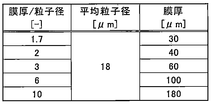
- the thickness of the wavelength conversion member 100 is preferably as shown in the following table.
- the thermal resistance representing the difficulty in transferring heat depends on the thickness when the thermal resistivity or thermal conductivity and area of the phosphor layer are constant, and the thermal resistance increases as the thickness increases.
- the thermal resistance that is, the thinner the thickness, the easier the heat is transmitted and the less heat storage occurs, and the temperature quenching due to heat generation (heat storage) can be suppressed.
- the translucent ceramic 121 is an inorganic binder for holding the phosphor particles 122, and is made of, for example, silica (SiO 2 ) or aluminum phosphate.
- silica SiO 2
- aluminum phosphate aluminum phosphate
- YAG phosphor yttrium / aluminum / garnet phosphor
- LAG phosphor lutetium / aluminum / garnet phosphor
- the phosphor particles can be selected from the following materials according to the design of the color to emit light.
- blue phosphors such as BaMgAl 10 O 17 : Eu, ZnS: Ag, Cl, BaAl 2 S 4 : Eu or CaMgSi 2 O 6 : Eu, Zn 2 SiO 4 : Mn, (Y, Gd) BO 3 : Tb, ZnS: Cu, Al, (M1) 2 SiO 4 : Eu, (M1) (M2) 2 S: Eu, (M3) 3 Al 5 O 12 : Ce, SiAlON: Eu, CaSiAlON: Eu, (M1) Si 2 O 2 N: Eu or (Ba, Sr, Mg) 2 SiO 4 : Yellow or green phosphor such as Eu, Mn, (M1) 3 SiO 5 : Eu or (M1) S: Eu, yellow orange or red phosphor, (Y, Gd) BO 3 : Eu, Y 2 O 2 S: Eu, (M1) 2 Si 5 N 8
- M1 includes at least one of the group consisting of Ba, Ca, Sr and Mg
- M2 includes at least one of Ga and Al
- M3 includes Y, Gd
- At least one of the group consisting of Lu and Te is included.
- said fluorescent substance particle is an example and the fluorescent substance particle used for a wavelength conversion member is not necessarily restricted above.
- the porosity of the phosphor layer 120 is preferably 30% or more and 70% or less. Since many pores are formed in the phosphor layer 120, even if the phosphor layer 120 is thin, light is dispersed inside, and the phosphor particles 122 are efficiently irradiated with the light source light.
- the thickness of the phosphor layer 120 is preferably such that the ratio of the thickness of the phosphor layer to the average particle diameter of the phosphor particles is in a predetermined range according to the average particle diameter of the phosphor particles 122. Since the film thickness is less than a predetermined multiple of the particle diameter of the phosphor particles, the density of the number of particles in the phosphor layer 120 does not become too high, and the thermal resistance of the grain boundaries can be reduced. On the other hand, since the film thickness is a predetermined multiple or more with respect to the particle diameter of the phosphor particles, the structure in the phosphor layer 120 can be made uniform, the intensity of the phosphor layer 120 can be maintained, and uniform light can be obtained. it can.
- the wavelength conversion member 100 has a luminous efficiency maintenance ratio of 70% or more when the light source light has a power density of 20 W / mm 2 .
- the light-emitting device 10 in which the fluorescence performance does not deteriorate even when the light is emitted at a high output can be configured.
- Such a light emitting device 10 is expected to be highly effective when applied to lighting of public facilities such as factories, stadiums, and museums, or automobile headlamps.
- FIGS. 2A, 2B, and 2C are cross-sectional views showing the steps for producing the wavelength conversion member of the present invention.
- an inorganic binder for example, ethyl silicate obtained by dissolving a silicon precursor in ethanol can be used.
- the inorganic binder is obtained by reacting a raw material containing at least one member selected from the group consisting of a silicon oxide precursor that becomes silicon oxide by hydrolysis or oxidation, a silicate compound, silica, and amorphous silica at room temperature, or Or obtained by heat treatment at a temperature of 500 ° C. or lower.
- a silicon oxide precursor that becomes silicon oxide by hydrolysis or oxidation
- a silicate compound silica
- amorphous silica at room temperature
- heat treatment at a temperature of 500 ° C. or lower.
- the silicon oxide precursor include those mainly composed of perhydropolysilazane, ethyl silicate, and methyl silicate.
- a high boiling point solvent such as butanol, isophorone, terpineol, glycerin or the like can be used.
- particles such as YAG and LAG can be used as the phosphor particles.
- the type and amount of the phosphor particles are adjusted according to the irradiation light to be obtained with respect to the light source light. For example, when white light is to be obtained with respect to blue light, an appropriate amount of phosphor particles that emit green light, red light, or yellow light by excitation with blue light is selected.
- a paste (ink) 410 is prepared by mixing these inorganic binder, solvent, and phosphor particles.
- a ball mill or the like can be used for mixing.
- a base material of an inorganic material is prepared.
- Aluminum can be used for the substrate.
- the substrate is preferably plate-shaped.
- a transmission type wavelength conversion member can also be produced by using glass, sapphire, or the like for the substrate.
- the obtained paste 410 is applied to the base 110 using a screen printing method so that the film thickness is in the range shown in the above table with respect to the average particle diameter.
- Screen printing can be performed by pressing the paste 410 with the ink squeegee 510 against the silk screen 520 stretched around the frame.
- the screen printing method there are a spray method, a drawing method using a dispenser, and an ink jet method, but the screen printing method is preferable in order to stably form a thin phosphor layer.
- the printed paste 410 is dried and heat-treated in the furnace 600, so that the solvent is removed and the organic content of the inorganic binder is removed to oxidize the main metal in the inorganic binder (in the case where the main metal is Si, SiO 2 In this case, the phosphor layer 120 and the substrate 110 are bonded. In this way, a wavelength conversion member can be obtained.
- the light emitting device can be manufactured by appropriately arranging a wavelength conversion member using a base material suitable for reflection with respect to a light source such as an LED.
- a wavelength conversion member was prepared as follows. Pastes made by mixing ethyl silicate and terpineol with YAG phosphor particles (average particle size 18 ⁇ m) were applied to glass, sapphire, and aluminum plates as base materials to a thickness of 40 ⁇ m using a screen printing method. The sample of the wavelength conversion member was obtained by coating and heat treatment.
- the transmissive evaluation system 700 includes a light source 710, a plano-convex lens 720, a biconvex lens 730, a bandpass filter 735, and a power meter 740.
- the band-pass filter 735 is a filter that cuts light having a wavelength of 480 nm or less, and a biconvex lens and a power meter are used to separate transmitted light source light (excitation light) from fluorescence when measuring the emission intensity of fluorescence. It is installed between.
- the light source light that has entered the planar convex lens 720 is condensed on the focal point on the wavelength conversion member 100. Then, the radiated light generated from the wavelength conversion member 100 is condensed by the biconvex lens 730, and the intensity of the light obtained by cutting the wavelength of 480 nm or less is measured by the power meter 740. This measured value is defined as fluorescence emission intensity.
- the reflection-type evaluation system 800 has the same components as the evaluation system 700, but each of the reflection-type evaluation systems 800 is configured so that the reflected light from the wavelength conversion member 100 can be collected and measured. The element is placed. By condensing the laser beam with a lens and reducing the irradiation area, the energy density per unit area can be increased even with a low-power laser. This energy density is defined as the laser power density.
- the wavelength conversion member was evaluated appropriately using the above-described two types of evaluation systems 700 and 800 properly.
- the glass or sapphire substrate sample was used, and in the reflection-type evaluation system 800, an aluminum substrate sample was used.
- the fluorescence emission intensity is the relative intensity obtained by making the numbers shown on the luminance meter dimensionless when the above evaluation system is used, and the emission efficiency maintenance rate is low enough to ignore the effects of heat generation and heat storage. This is the ratio of the light emission efficiency to each laser power density when the light emission efficiency is 100% at the laser power density.
- aluminum has a higher thermal conductivity than glass. Therefore, in the aluminum base material, it is considered that heat generation from the phosphor particles is difficult to store in the wavelength conversion member, and quenching of the phosphor is suppressed.
- extinction can be suppressed by the sapphire base material rather than the aluminum base material with high heat conductivity. This is presumably because in the measurement of the transmission type sapphire base material, the laser is incident from the base material, so that the heat stored in the phosphor is immediately radiated to the base material.
- the sapphire substrate can suppress quenching more than the aluminum substrate having a high thermal conductivity. This is presumably because in the measurement of the transmission type sapphire base material, the laser is incident from the base material, so that the heat stored in the phosphor is immediately radiated to the base material.
- FIGS. 5A and 5B are graphs showing the light emission characteristics when the thickness of the phosphor layer is changed with respect to a certain phosphor particle diameter as shown in the table below. For each condition, the fluorescence emission intensity and the emission efficiency maintenance ratio with respect to the laser power density are shown.
- the fluorescence emission intensity increased as the laser input value increased with the thickness of all the phosphor layers / the average particle diameter of the phosphor particles.
- the fluorescence emission intensity is almost the same emission intensity regardless of the ratio of the phosphor layer thickness to the average particle size until the saturation point is reached, and the ratio of the phosphor layer thickness to the average particle size is It was confirmed that the smaller the value, the higher the luminous efficiency maintenance rate can be maintained.
- the maintenance of the luminous efficiency it is considered that the smaller the ratio of the phosphor layer thickness to the average particle diameter of the phosphor particles, the more effective the prevention of heat storage due to the smaller number of contacts between the particles.
- the phosphor generates heat as the value of the laser power density increases, and when the temperature of the phosphor layer rises, quenching occurs and the luminous efficiency decreases.
- the ratio of the average particle diameter of the phosphor particles and the thickness of the phosphor layer / the average particle diameter of the phosphor particles satisfied the judgment criteria within the range of Table 1. .
- FIGS. 6A and 6B are graphs showing the emission characteristics when the average particle diameter of the phosphor particles is changed. As shown in FIGS. 6A and 6B, it was confirmed that the larger the average particle diameter of the phosphor particles, the higher the fluorescence emission intensity and the emission efficiency maintenance ratio. It is considered that the larger the phosphor particles are, the higher the conversion efficiency is, and it is due to the effects of both that the number of contacts between the phosphor particles is reduced and heat storage can be prevented.
- the obtained wavelength conversion member was subjected to porosity calculation and laser irradiation test, and the relationship between the porosity, fluorescence emission intensity, and saturation point was confirmed.
- the porosity was calculated by defining the ratio of the volume of the void portion in the phosphor film to the apparent volume obtained by connecting the outermost surfaces of the phosphor particles on the phosphor film with a straight line.
- the volume of the void portion was calculated by subtracting the volume of the solid component from the apparent volume.
- FIGS. 7A and 7B are graphs showing the relationship between the porosity, the fluorescence emission intensity, and the saturation point, respectively. From the relationship between the porosity and the fluorescence emission intensity and the saturation point shown in FIGS. 7A and 7B, it is confirmed that the fluorescence emission intensity and the saturation point are stable when the porosity is in the range of 30 to 70%. It was done. If the porosity is less than 30%, peeling occurs due to heat treatment during production, and it is difficult to produce the wavelength conversion member. The cause of this peeling is considered to be due to the difference in thermal expansion between the substrate and the phosphor layer. In addition, when the porosity is 70% or more, it is difficult to maintain the structure of the phosphor layer and it is difficult to manufacture.
- the wavelength conversion member (film thickness 30 ⁇ m) of the present invention obtained by the above-described method for producing a wavelength conversion member and a sintered body (square plate shape having a side of 20.0 mm and a thickness of 1.0 mm)
- the phosphor plate was irradiated with a laser using a reflective evaluation system 800, and the fluorescence emission intensity with respect to the laser power density was examined to confirm the change in the fluorescence emission intensity due to the porosity.
- the porosity was calculated by defining the ratio of the volume of the void portion in the phosphor film to the apparent volume connecting the outermost surfaces of the phosphor particles on the phosphor film with a straight line.
- the volume of the void portion was calculated by subtracting the volume of the solid component from the apparent volume.
- the porosity of the wavelength conversion member was 40%, and the porosity of the sintered body was less than 1%.
- FIGS. 8A and 8B are graphs showing the light emission characteristics of the sintered body and the wavelength conversion member, respectively. It was confirmed that the wavelength conversion member shown in FIGS. 8A and 8B has higher fluorescence emission intensity. This is probably because light scattering occurred due to voids in the layer of the wavelength conversion member, and the fluorescence emission intensity was increased in order to efficiently convert the light. On the other hand, it is considered that a sintered body with few voids is dense, and therefore has little light scattering inside and transmits laser light.
- the laser is still transmitted even though the thickness is 1 mm (1000 ⁇ m), whereas the wavelength conversion member of the present invention is optimal even though the thickness is 30 ⁇ m. Therefore, it is considered to be very effective because the fluorescent light can be efficiently extracted by scattering light.
Landscapes
- Engineering & Computer Science (AREA)
- Physics & Mathematics (AREA)
- Chemical & Material Sciences (AREA)
- General Physics & Mathematics (AREA)
- Optics & Photonics (AREA)
- Organic Chemistry (AREA)
- Materials Engineering (AREA)
- Microelectronics & Electronic Packaging (AREA)
- General Engineering & Computer Science (AREA)
- Inorganic Chemistry (AREA)
- Manufacturing & Machinery (AREA)
- Computer Hardware Design (AREA)
- Electromagnetism (AREA)
- Power Engineering (AREA)
- Condensed Matter Physics & Semiconductors (AREA)
- Spectroscopy & Molecular Physics (AREA)
- Semiconductor Lasers (AREA)
- Led Device Packages (AREA)
- Optical Filters (AREA)
- Luminescent Compositions (AREA)
Abstract
Description
図1は、反射型の発光装置10を示す模式図である。図1に示すように、発光装置10は、光源50および波長変換部材100を備え、例えば波長変換部材100で反射した光源光および波長変換部材100内で光源光による励起で発生した光を合わせて照射光を放射している。照射光は例えば白色光とすることができる。
波長変換部材100は、基材110および蛍光体層120を備え、板状に形成され、光源光を基材110で反射させつつ、光源光に励起して波長の異なる光を発生させる。例えば、青色光を反射させつつ、緑と赤や黄色の蛍光を発生させて白色光を放射できる。基材110は、板状に形成され、例えば、光源光を反射させる無機材料で構成できる。基材110は、アルミニウムからなることが好ましい。高い熱伝導性を有する基材110を採用することで、蛍光体層120の蓄熱を抑え、蛍光体粒子の温度上昇を抑制でき、温度消光を防止できる。

図2(a)、(b)、(c)は、それぞれ本発明の波長変換部材の作製工程を示す断面図である。まず無機バインダ、溶剤、蛍光体粒子を準備する。好ましい無機バインダとして、例えばエタノールにシリコンの前駆体を溶かして得られたエチルシリケートを用いることができる。
(1.基材に対する消光状態の確認)
(1-1)試料の作製方法
まず、以下のように波長変換部材を作製した。エチルシリケートとテルピネオールをYAG蛍光体粒子(平均粒子径18μm)と混合して作製されたペーストを、スクリーン印刷法を用いて40μmの厚みになるよう基材となるガラス、サファイア、アルミニウムの板にそれぞれ塗布し、熱処理して波長変換部材の試料を得た。
上記作製方法により得られた波長変換部材にレーザを照射し、レーザ入力値に対する蛍光の発光強度と発光効率維持率を調べた。図3(a)、(b)は、それぞれ波長変換部材に対する透過型、反射型の評価システム700、800を示す断面図である。図3(a)に示すように、透過型の評価システム700は、光源710、平面凸レンズ720、両凸レンズ730、バンドパスフィルタ735、パワーメータ740で構成されている。なお、バンドパスフィルタ735は、波長480nm以下の光をカットするフィルタであり、蛍光の発光強度を測定する際に、透過した光源光(励起光)を蛍光と切り分けるために、両凸レンズとパワーメータの間に設置される。
上記の評価結果として基材に対する発光特性を確認できた。図4(a)、(b)は、それぞれ基材を変えたときの発光特性を示すグラフである。3種の基材で一定のレーザパワー密度まではパワー密度の増加に伴い蛍光の発光強度がほぼ比例の関係で増加していくことが確認された。サファイア基材ではレーザパワー密度が48W/mm2、アルミニウム基材では27W/mm2、ガラス基材では11W/mm2以上で発光が減少した。
(2-1)試料の作製方法
エチルシリケートとテルピネオールをYAG系の蛍光体粒子(平均粒子径18μm)と混合して作製されたペーストを、スクリーン印刷法を用いて30、40、60、100、180μmの厚みになるよう基材となるAl+Ag板に塗布し波長変換部材の試料を得た。Al+Ag基材は、主にAl合金とAg膜とで構成されている(Alanod製 MIRO2 SILVER使用)。
上記の波長変換部材の作製方法により得られた波長変換部材について、反射型の評価システムを用いてレーザ照射を行ない、レーザパワー密度に対する蛍光の発光強度および発光効率維持率を調べた。
上記の評価結果として蛍光体層の発光特性を確認できた。図5(a)、(b)は、下表の通りにそれぞれ一定の蛍光体粒子径に対して蛍光体層の厚みを変えたときの発光特性を示すグラフである。各条件について、レーザパワー密度に対する蛍光の発光強度および発光効率維持率をそれぞれ示している。
(3-1)試料の作成方法
エチルシリケートとテルピネオールをYAG系蛍光体粒子と混合して作製されたペーストを、スクリーン印刷法を用いて基材となるアルミニウム板(反射型)に塗布した。
上記の波長変換部材の作製方法により得られた波長変換部材について、反射型の評価システム800を用いてレーザ照射を行ない、20W/mm2のレーザパワー密度における発光効率維持率を調べた。
下表は、条件と結果をまとめた表である。

(4-1)試料の作製方法
エチルシリケートとテルピネオールをYAG系蛍光体粒子と混合して作製されたペーストを、スクリーン印刷法を用いて膜厚が30μmになるよう基材となるアルミニウム板に塗布した。蛍光体粒子は、6、13、18μmの3種の平均粒子径のものを用いた。
上記の波長変換部材の作製方法により得られたアルミニウム基材の波長変換部材について、反射型の評価システム800を用いてレーザ照射を行ない、レーザパワー密度に対する蛍光の発光強度および発光効率維持率を調べた。
図6(a)、(b)は、それぞれ蛍光体粒子の平均粒子径を変えたときの発光特性を示すグラフである。図6(a)、(b)に示すように、蛍光体粒子の平均粒子径が大きいほど蛍光の発光強度、発光効率維持率が高いことが確認された。蛍光体粒子が大きいほど、変換効率が高いこと、また、蛍光体粒子同士の接点が少なくなり蓄熱を防止できたことの双方の効果によるものと考えられる。
(5-1)試料の作製方法
エチルシリケートとテルピネオールをYAG系蛍光体粒子(平均粒子径18μm)と混合して作製されたペーストを、スクリーン印刷法を用いて30μmの厚みになるよう基材となるアルミニウム板に塗布し波長変換部材の試料を得た。
得られた波長変換部材について空隙率の計算とレーザ照射試験を行ない、空隙率と蛍光の発光強度および飽和点の関係を確認した。空隙率は、蛍光体膜上の蛍光体粒子の最表面を直線で結んだ見かけ上の体積に対する、蛍光体膜内の空隙部分の体積の割合と定義して算出した。空隙部分の体積は、見かけ上の体積から固体成分の体積を差し引き算出した。
図7(a)、(b)は、それぞれ空隙率と蛍光の発光強度および飽和点の関係を示すグラフである。図7(a)、(b)に示す空隙率と蛍光の発光強度および飽和点の関係より、空隙率が30~70%の範囲では蛍光の発光強度、飽和点が安定していることが確認された。空隙率が30%未満では製作時の熱処理により、剥離が発生してしまい、波長変換部材は製造困難である。この剥離の原因は、基材と蛍光体層との熱膨張の差によるものと考えられる。また、空隙率が70%以上では蛍光体層の構造の維持が難しく製造が困難である。
(6-1)評価方法
上記の波長変換部材の作製方法により得られた本発明の波長変換部材(膜厚30μm)と焼結体(一辺20.0mm、厚さ1.0mmの正方板形状)の蛍光体プレートについて、反射型の評価システム800を用いてレーザ照射を行ない、レーザパワー密度に対する蛍光の発光強度を調べて空隙率による蛍光の発光強度の変化を確認した。
図8(a)、(b)は、それぞれ焼結体と波長変換部材の発光特性を示すグラフである。図8(a)、(b)に示す波長変換部材のほうが、蛍光の発光強度が高いことが確認された。これは、波長変換部材の層内の空隙により光の散乱が起こり、効率よく光を変換するために蛍光の発光強度が高くなったと考えられる。一方で、空隙の少ない焼結体は、緻密であるため内部での光の散乱が少なくレーザ光を透過してしまうと考えられる。
50 光源
100 波長変換部材
110 基材
120 蛍光体層
121 透光性セラミックス
122 蛍光体粒子
410 ペースト
510 インキスキージ
520 シルクスクリーン
600 炉
700、800 評価システム
710 光源
720 平面凸レンズ
730 両凸レンズ
735 バンドパスフィルタ
740 パワーメータ
Claims (5)
- 特定範囲の波長の光を他の波長の光に変換するとともに、反射面により光を反射して照射光とする反射型の波長変換部材であって、
無機材料からなる基材と、
前記基材上に設けられ、吸収光に対し変換光を発する蛍光体粒子と前記蛍光体粒子同士を結合する透光性セラミックスとからなる蛍光体層と、を備え、
前記蛍光体層の厚みと前記蛍光体粒子の平均粒子径との比が30未満であり、
特定範囲の波長の光源光に対し、前記光源光が20W/mm2のパワー密度であるときに、前記蛍光体層の発光効率維持率が70%以上であり、
前記基材または自部材に隣接する反射板の表面を前記変換光の反射面とすることを特徴とする波長変換部材。 - 以下の条件を満たすことを特徴とする請求項1に記載の波長変換部材。
(a)前記蛍光体粒子の平均粒子径が1μm未満の場合は、前記蛍光体層の厚みと前記蛍光体粒子の平均粒子径との比が30未満であること。
(b)前記蛍光体粒子の平均粒子径が1μm以上5μm未満の場合は、前記蛍光体層の厚みと前記蛍光体粒子の平均粒子径との比が15未満であること。
(c)前記蛍光体粒子の平均粒子径が5μm以上10μm未満の場合は、前記蛍光体層の厚みと前記蛍光体粒子の平均粒子径との比が10未満であること。
(d)前記蛍光体粒子の平均粒子径が10μm以上の場合は、前記蛍光体層の厚みと前記蛍光体粒子の平均粒子径との比が5未満であること。 - 前記蛍光体層の、前記蛍光体粒子の最表面および前記基材と接する平面で挟まれた一定厚さの層の見かけ上の体積に対して、前記見かけ上の体積から前記見かけ上の体積内に含まれる固体成分の体積を差し引くことで算出された空隙部分の体積の割合を空隙率と定義した場合に、その前記空隙率は、30~70%であることを特徴とする請求項1または請求項2のいずれかに記載の波長変換部材。
- 前記基材は、アルミニウムからなることを特徴とする請求項1から請求項3のいずれかに記載の波長変換部材。
- 特定範囲の波長の光源光を発生させる光源と、
前記光源光を吸収し、他の波長の光に変換し発光する請求項1から請求項4のいずれかに記載の波長変換部材と、を備えることを特徴とする発光装置。
Priority Applications (5)
| Application Number | Priority Date | Filing Date | Title |
|---|---|---|---|
| JP2017539380A JP6524474B2 (ja) | 2016-01-22 | 2017-01-13 | 波長変換部材および発光装置 |
| EP17741319.2A EP3407101B1 (en) | 2016-01-22 | 2017-01-13 | Wavelength conversion member and light-emitting device |
| CN201780007590.2A CN108474881B (zh) | 2016-01-22 | 2017-01-13 | 波长转换构件及发光装置 |
| US16/070,974 US10508801B2 (en) | 2016-01-22 | 2017-01-13 | Wavelength conversion member and light-emitting device |
| KR1020187020385A KR102044140B1 (ko) | 2016-01-22 | 2017-01-13 | 파장 변환 부재 및 발광 장치 |
Applications Claiming Priority (2)
| Application Number | Priority Date | Filing Date | Title |
|---|---|---|---|
| JP2016011100 | 2016-01-22 | ||
| JP2016-011100 | 2016-01-22 |
Publications (1)
| Publication Number | Publication Date |
|---|---|
| WO2017126441A1 true WO2017126441A1 (ja) | 2017-07-27 |
Family
ID=59362337
Family Applications (1)
| Application Number | Title | Priority Date | Filing Date |
|---|---|---|---|
| PCT/JP2017/001078 WO2017126441A1 (ja) | 2016-01-22 | 2017-01-13 | 波長変換部材および発光装置 |
Country Status (7)
| Country | Link |
|---|---|
| US (1) | US10508801B2 (ja) |
| EP (1) | EP3407101B1 (ja) |
| JP (1) | JP6524474B2 (ja) |
| KR (1) | KR102044140B1 (ja) |
| CN (1) | CN108474881B (ja) |
| TW (1) | TWI677115B (ja) |
| WO (1) | WO2017126441A1 (ja) |
Cited By (1)
| Publication number | Priority date | Publication date | Assignee | Title |
|---|---|---|---|---|
| JPWO2021221062A1 (ja) * | 2020-04-28 | 2021-11-04 |
Families Citing this family (5)
| Publication number | Priority date | Publication date | Assignee | Title |
|---|---|---|---|---|
| CN208239722U (zh) | 2018-05-24 | 2018-12-14 | 中强光电股份有限公司 | 波长转换轮、照明系统及投影装置 |
| CN110416387B (zh) * | 2019-06-28 | 2020-12-01 | 苏州紫灿科技有限公司 | 一种高散热白光激光片及制备方法 |
| JP7429346B2 (ja) * | 2019-10-03 | 2024-02-08 | 国立研究開発法人物質・材料研究機構 | 波長変換部材 |
| CN113917776B (zh) * | 2020-07-09 | 2023-03-24 | 中强光电股份有限公司 | 波长转换装置以及投影装置 |
| WO2022251195A1 (en) * | 2021-05-24 | 2022-12-01 | W. L. Gore & Associates, Inc. | Photoluminescent composites and processes for fabricating the same |
Citations (10)
| Publication number | Priority date | Publication date | Assignee | Title |
|---|---|---|---|---|
| JP2007262375A (ja) * | 2006-03-30 | 2007-10-11 | Kyocera Corp | 波長変換器および発光装置 |
| JP2008043754A (ja) * | 2003-12-22 | 2008-02-28 | Nichia Chem Ind Ltd | 発光装置及び内視鏡装置 |
| JP2012185403A (ja) * | 2011-03-07 | 2012-09-27 | Seiko Epson Corp | 発光素子とその製造方法、光源装置、およびプロジェクター |
| JP2013247067A (ja) * | 2012-05-29 | 2013-12-09 | Nichia Chem Ind Ltd | 色変換用無機成形体及びその製造方法、並びに発光装置 |
| JP2014241431A (ja) | 2013-05-16 | 2014-12-25 | 株式会社日本セラテック | 発光装置の製造方法 |
| JP2015065425A (ja) | 2013-08-29 | 2015-04-09 | 株式会社日本セラテック | 発光装置及びその製造方法 |
| JP2015090887A (ja) | 2013-11-05 | 2015-05-11 | 株式会社日本セラテック | 発光素子及び発光装置 |
| JP2015094777A (ja) | 2013-11-08 | 2015-05-18 | 日本電気硝子株式会社 | プロジェクター用蛍光ホイール、その製造方法及びプロジェクター用発光デバイス |
| JP2015119172A (ja) | 2013-11-13 | 2015-06-25 | 株式会社日本セラテック | 発光素子、発光装置、及びそれらの製造方法 |
| JP2015138839A (ja) | 2014-01-21 | 2015-07-30 | 豊田合成株式会社 | 発光装置及びその製造方法 |
Family Cites Families (10)
| Publication number | Priority date | Publication date | Assignee | Title |
|---|---|---|---|---|
| US9631782B2 (en) * | 2010-02-04 | 2017-04-25 | Xicato, Inc. | LED-based rectangular illumination device |
| JPWO2011155614A1 (ja) * | 2010-06-11 | 2013-08-15 | 旭硝子株式会社 | 透光性積層体およびそれを用いた太陽電池モジュール |
| CN102959744B (zh) * | 2011-06-29 | 2015-08-19 | 松下电器产业株式会社 | 发光元件的制造方法及发光元件的制造装置 |
| TWI523278B (zh) * | 2011-08-05 | 2016-02-21 | 晶元光電股份有限公司 | 波長轉換結構及其製造方法以及包含此波長轉換結構之發光裝置 |
| TWI505515B (zh) * | 2011-08-19 | 2015-10-21 | Epistar Corp | 發光裝置及其製造方法 |
| JPWO2013051281A1 (ja) * | 2011-10-07 | 2015-03-30 | コニカミノルタ株式会社 | Led装置の製造方法、およびそれに用いる蛍光体分散液 |
| JP2014039006A (ja) | 2012-02-27 | 2014-02-27 | Mitsubishi Chemicals Corp | 波長変換部材及びこれを用いた半導体発光装置 |
| JP5966529B2 (ja) | 2012-04-02 | 2016-08-10 | 日亜化学工業株式会社 | 波長変換用無機成形体及び発光装置 |
| CN103367611B (zh) | 2012-03-28 | 2017-08-08 | 日亚化学工业株式会社 | 波长变换用无机成型体及其制造方法以及发光装置 |
| CN104676491A (zh) * | 2013-11-29 | 2015-06-03 | 台达电子工业股份有限公司 | 波长转换装置 |
-
2017
- 2017-01-13 JP JP2017539380A patent/JP6524474B2/ja active Active
- 2017-01-13 EP EP17741319.2A patent/EP3407101B1/en active Active
- 2017-01-13 US US16/070,974 patent/US10508801B2/en active Active
- 2017-01-13 WO PCT/JP2017/001078 patent/WO2017126441A1/ja active Application Filing
- 2017-01-13 CN CN201780007590.2A patent/CN108474881B/zh active Active
- 2017-01-13 KR KR1020187020385A patent/KR102044140B1/ko active IP Right Grant
- 2017-01-20 TW TW106102006A patent/TWI677115B/zh active
Patent Citations (11)
| Publication number | Priority date | Publication date | Assignee | Title |
|---|---|---|---|---|
| JP2008043754A (ja) * | 2003-12-22 | 2008-02-28 | Nichia Chem Ind Ltd | 発光装置及び内視鏡装置 |
| JP2007262375A (ja) * | 2006-03-30 | 2007-10-11 | Kyocera Corp | 波長変換器および発光装置 |
| JP2012185403A (ja) * | 2011-03-07 | 2012-09-27 | Seiko Epson Corp | 発光素子とその製造方法、光源装置、およびプロジェクター |
| JP2013247067A (ja) * | 2012-05-29 | 2013-12-09 | Nichia Chem Ind Ltd | 色変換用無機成形体及びその製造方法、並びに発光装置 |
| JP2014241431A (ja) | 2013-05-16 | 2014-12-25 | 株式会社日本セラテック | 発光装置の製造方法 |
| JP2015038960A (ja) | 2013-05-16 | 2015-02-26 | 株式会社日本セラテック | 発光装置 |
| JP2015065425A (ja) | 2013-08-29 | 2015-04-09 | 株式会社日本セラテック | 発光装置及びその製造方法 |
| JP2015090887A (ja) | 2013-11-05 | 2015-05-11 | 株式会社日本セラテック | 発光素子及び発光装置 |
| JP2015094777A (ja) | 2013-11-08 | 2015-05-18 | 日本電気硝子株式会社 | プロジェクター用蛍光ホイール、その製造方法及びプロジェクター用発光デバイス |
| JP2015119172A (ja) | 2013-11-13 | 2015-06-25 | 株式会社日本セラテック | 発光素子、発光装置、及びそれらの製造方法 |
| JP2015138839A (ja) | 2014-01-21 | 2015-07-30 | 豊田合成株式会社 | 発光装置及びその製造方法 |
Non-Patent Citations (1)
| Title |
|---|
| See also references of EP3407101A4 |
Cited By (2)
| Publication number | Priority date | Publication date | Assignee | Title |
|---|---|---|---|---|
| JPWO2021221062A1 (ja) * | 2020-04-28 | 2021-11-04 | ||
| WO2021221062A1 (ja) * | 2020-04-28 | 2021-11-04 | 京セラ株式会社 | 波長変換素子および波長変換素子の製造方法 |
Also Published As
| Publication number | Publication date |
|---|---|
| CN108474881A (zh) | 2018-08-31 |
| US20190024879A1 (en) | 2019-01-24 |
| TWI677115B (zh) | 2019-11-11 |
| US10508801B2 (en) | 2019-12-17 |
| CN108474881B (zh) | 2021-02-02 |
| JP6524474B2 (ja) | 2019-06-05 |
| EP3407101B1 (en) | 2024-05-29 |
| EP3407101A1 (en) | 2018-11-28 |
| KR102044140B1 (ko) | 2019-11-13 |
| TW201733170A (zh) | 2017-09-16 |
| EP3407101A4 (en) | 2019-10-09 |
| KR20180095645A (ko) | 2018-08-27 |
| JPWO2017126441A1 (ja) | 2018-01-25 |
Similar Documents
| Publication | Publication Date | Title |
|---|---|---|
| TWI753889B (zh) | 波長轉換構件、其製造方法及發光裝置 | |
| WO2017126441A1 (ja) | 波長変換部材および発光装置 | |
| TWI669375B (zh) | 波長轉換構件及發光裝置 | |
| US10590341B2 (en) | Wavelength conversion member, production method therefor, and light emitting device | |
| WO2019031016A1 (ja) | 波長変換部材および発光装置 | |
| JP6990065B2 (ja) | 波長変換部材、その製造方法および発光装置 | |
| JP2018131577A (ja) | 波長変換部材 | |
| JP2021103247A (ja) | 波長変換部材および発光装置 | |
| JP2021099415A (ja) | 波長変換部材および発光装置 |
Legal Events
| Date | Code | Title | Description |
|---|---|---|---|
| ENP | Entry into the national phase |
Ref document number: 2017539380 Country of ref document: JP Kind code of ref document: A |
|
| 121 | Ep: the epo has been informed by wipo that ep was designated in this application |
Ref document number: 17741319 Country of ref document: EP Kind code of ref document: A1 |
|
| ENP | Entry into the national phase |
Ref document number: 20187020385 Country of ref document: KR Kind code of ref document: A |
|
| WWE | Wipo information: entry into national phase |
Ref document number: 1020187020385 Country of ref document: KR |
|
| NENP | Non-entry into the national phase |
Ref country code: DE |
|
| WWE | Wipo information: entry into national phase |
Ref document number: 2017741319 Country of ref document: EP |
|
| ENP | Entry into the national phase |
Ref document number: 2017741319 Country of ref document: EP Effective date: 20180822 |