WO2017122460A1 - Dry film and printed wiring board - Google Patents
Dry film and printed wiring board Download PDFInfo
- Publication number
- WO2017122460A1 WO2017122460A1 PCT/JP2016/086192 JP2016086192W WO2017122460A1 WO 2017122460 A1 WO2017122460 A1 WO 2017122460A1 JP 2016086192 W JP2016086192 W JP 2016086192W WO 2017122460 A1 WO2017122460 A1 WO 2017122460A1
- Authority
- WO
- WIPO (PCT)
- Prior art keywords
- resin
- resin layer
- dry film
- epoxy resin
- film
- Prior art date
Links
Images


Classifications
-
- B—PERFORMING OPERATIONS; TRANSPORTING
- B32—LAYERED PRODUCTS
- B32B—LAYERED PRODUCTS, i.e. PRODUCTS BUILT-UP OF STRATA OF FLAT OR NON-FLAT, e.g. CELLULAR OR HONEYCOMB, FORM
- B32B27/00—Layered products comprising a layer of synthetic resin
- B32B27/38—Layered products comprising a layer of synthetic resin comprising epoxy resins
-
- B—PERFORMING OPERATIONS; TRANSPORTING
- B32—LAYERED PRODUCTS
- B32B—LAYERED PRODUCTS, i.e. PRODUCTS BUILT-UP OF STRATA OF FLAT OR NON-FLAT, e.g. CELLULAR OR HONEYCOMB, FORM
- B32B27/00—Layered products comprising a layer of synthetic resin
- B32B27/18—Layered products comprising a layer of synthetic resin characterised by the use of special additives
- B32B27/20—Layered products comprising a layer of synthetic resin characterised by the use of special additives using fillers, pigments, thixotroping agents
-
- C—CHEMISTRY; METALLURGY
- C08—ORGANIC MACROMOLECULAR COMPOUNDS; THEIR PREPARATION OR CHEMICAL WORKING-UP; COMPOSITIONS BASED THEREON
- C08K—Use of inorganic or non-macromolecular organic substances as compounding ingredients
- C08K9/00—Use of pretreated ingredients
- C08K9/04—Ingredients treated with organic substances
- C08K9/06—Ingredients treated with organic substances with silicon-containing compounds
-
- C—CHEMISTRY; METALLURGY
- C08—ORGANIC MACROMOLECULAR COMPOUNDS; THEIR PREPARATION OR CHEMICAL WORKING-UP; COMPOSITIONS BASED THEREON
- C08L—COMPOSITIONS OF MACROMOLECULAR COMPOUNDS
- C08L63/00—Compositions of epoxy resins; Compositions of derivatives of epoxy resins
-
- G—PHYSICS
- G03—PHOTOGRAPHY; CINEMATOGRAPHY; ANALOGOUS TECHNIQUES USING WAVES OTHER THAN OPTICAL WAVES; ELECTROGRAPHY; HOLOGRAPHY
- G03F—PHOTOMECHANICAL PRODUCTION OF TEXTURED OR PATTERNED SURFACES, e.g. FOR PRINTING, FOR PROCESSING OF SEMICONDUCTOR DEVICES; MATERIALS THEREFOR; ORIGINALS THEREFOR; APPARATUS SPECIALLY ADAPTED THEREFOR
- G03F7/00—Photomechanical, e.g. photolithographic, production of textured or patterned surfaces, e.g. printing surfaces; Materials therefor, e.g. comprising photoresists; Apparatus specially adapted therefor
- G03F7/004—Photosensitive materials
- G03F7/027—Non-macromolecular photopolymerisable compounds having carbon-to-carbon double bonds, e.g. ethylenic compounds
-
- H—ELECTRICITY
- H05—ELECTRIC TECHNIQUES NOT OTHERWISE PROVIDED FOR
- H05K—PRINTED CIRCUITS; CASINGS OR CONSTRUCTIONAL DETAILS OF ELECTRIC APPARATUS; MANUFACTURE OF ASSEMBLAGES OF ELECTRICAL COMPONENTS
- H05K3/00—Apparatus or processes for manufacturing printed circuits
- H05K3/22—Secondary treatment of printed circuits
- H05K3/28—Applying non-metallic protective coatings
- H05K3/281—Applying non-metallic protective coatings by means of a preformed insulating foil
-
- B—PERFORMING OPERATIONS; TRANSPORTING
- B32—LAYERED PRODUCTS
- B32B—LAYERED PRODUCTS, i.e. PRODUCTS BUILT-UP OF STRATA OF FLAT OR NON-FLAT, e.g. CELLULAR OR HONEYCOMB, FORM
- B32B2457/00—Electrical equipment
- B32B2457/08—PCBs, i.e. printed circuit boards
-
- C—CHEMISTRY; METALLURGY
- C08—ORGANIC MACROMOLECULAR COMPOUNDS; THEIR PREPARATION OR CHEMICAL WORKING-UP; COMPOSITIONS BASED THEREON
- C08K—Use of inorganic or non-macromolecular organic substances as compounding ingredients
- C08K2201/00—Specific properties of additives
- C08K2201/002—Physical properties
- C08K2201/005—Additives being defined by their particle size in general
Definitions
- the present invention relates to a dry film and a printed wiring board, and more particularly to a dry film having a resin layer excellent in embedding property and flatness, and a printed wiring board having a cured product obtained by curing the dry film.
- a dry film has been used as one of means for forming a protective film or an insulating layer such as a solder resist or an interlayer insulating layer provided on a printed wiring board used in an electronic device or the like (for example, Patent Documents 1 to 3).
- a dry film has a resin layer obtained by applying a curable resin composition having desired characteristics on a carrier film and then undergoing a drying process, and generally protects the surface opposite to the carrier film.
- the protective film for carrying out is distribute
- the resin layer When laminating a resin layer of a dry film on a substrate, the resin layer is not sufficiently embedded in the unevenness of the circuit pattern on the substrate, and bubbles may be generated between the resin layer and the substrate. Such air bubbles sometimes impair the adhesion between the resin layer and the substrate.
- an object of the present invention is to provide a dry film having a resin layer excellent in embedding property and flatness, and a printed wiring board having a cured product obtained by curing the dry film.
- the melt viscosity at 100 ° C. is 60 to 5500 dPa ⁇ s
- the storage elastic modulus at 100 ° C. is 10 to 5500 Pa
- the liquid epoxy resin is 60% of the total amount of epoxy resin.
- the dry film of the present invention is a dry film having a film and a resin layer containing an epoxy resin formed on the film, and the resin layer has a melt viscosity of 60 to 5500 dPa ⁇ s at 100 ° C.
- the storage modulus of the resin layer is 80 to 5500 Pa at 100 ° C.
- the resin layer contains at least a liquid epoxy resin as the epoxy resin, Content of the said liquid epoxy resin is less than 60 mass% with respect to the said epoxy resin total mass, It is characterized by the above-mentioned.
- the amount of residual solvent in the resin layer is preferably 1.0 to 7.0% by mass.
- the dry film of the present invention contains at least two organic solvents selected from the group consisting of N, N-dimethylformamide, toluene, cyclohexanone, aromatic hydrocarbons having 8 or more carbon atoms, and methyl ethyl ketone in the resin layer. It is preferable.
- the resin layer further comprises at least one semi-solid epoxy resin selected from the group consisting of a bisphenol A type epoxy resin, a naphthalene type epoxy resin, and a phenol novolac type epoxy resin as the epoxy resin. It is preferable to include.
- the resin layer preferably contains a filler, and the filler has an average particle size of 0.1 to 10 ⁇ m.
- the resin layer contains a filler, and the content of the filler is 40 to 80% by mass per total resin layer (the total amount excluding the solvent when the resin layer contains a solvent). preferable.
- the resin layer includes a filler
- the filler includes a silane coupling agent having an epoxy group, a silane coupling agent having an amino group, a silane coupling agent having a mercapto group, and an isocyanate group.
- Surface treatment with at least one of a silane coupling agent having a vinyl group, a silane coupling agent having a vinyl group, a silane coupling agent having a styryl group, a silane coupling agent having an acrylic group, and a silane coupling agent having a methacryl group It is preferable that
- the cured product of the present invention is obtained by curing the resin layer of the dry film.
- the printed wiring board of the present invention is characterized by comprising the cured product.
- the present invention it is possible to provide a dry film having a resin layer excellent in embedding property and flatness, and a printed wiring board comprising a cured product obtained by curing the dry film.
- the dry film of the present invention is a dry film having a film and a resin layer formed on the film, wherein the resin layer has a melt viscosity of 60 to 5500 dPa ⁇ s at 100 ° C. And the resin layer contains at least a liquid epoxy resin as the epoxy resin, and the content of the liquid epoxy resin is 60% by mass with respect to the total amount of the epoxy resin. It is characterized by being less than.
- both the melt viscosity and the storage elastic modulus of the resin layer are adjusted to the above ranges, and the ratio of the liquid epoxy resin contained in the resin layer to the total amount of the epoxy resin is less than 60% by mass. As a result, embedding and flatness are remarkably improved.
- a cured film having a flat surface can be formed. Therefore, when a plating resist is formed on the dry film, omission of the plating resist line and development failure can be suppressed. . That is, according to the dry film of the present invention, a cured product having excellent plating resist formability can be obtained. As a result, a high-definition conductive circuit can be formed on the resin layer. On the other hand, when the melt viscosity of the resin layer of the dry film is less than 60 dPa ⁇ s at 100 ° C.
- the melt viscosity of the resin layer exceeds 5500 dPa ⁇ s at 100 ° C. or the storage elastic modulus of the resin layer exceeds 5500 Pa at 100 ° C., it becomes difficult to obtain flatness of the outer surface of the resin layer.
- the melt viscosity of the resin layer is preferably 400 to 3000 dPa ⁇ s at 100 ° C.
- the storage elastic modulus of the resin layer is preferably 100 to 3500 Pa at 100 ° C.
- the content of the liquid epoxy resin is 60% by mass or more with respect to the total amount of the epoxy resin, it is difficult to obtain the embedding property of the dry film and the flatness of the outer surface of the resin layer.
- melt viscosity of the resin layer is 3000 dPa ⁇ s or less at 100 ° C. and the storage elastic modulus of the resin layer is 3000 Pa or less at 100 ° C. because of excellent flatness and plating resist formation.
- melt viscosity of the resin layer is 100 dPa ⁇ s or more at 100 ° C. and the storage elastic modulus of the resin layer is 100 Pa or more at 100 ° C., it is preferable because bubbles are less likely to be entrained during lamination and the embedding property is more excellent. .
- the melt viscosity of the resin layer is 500 to 3000 dPa ⁇ s at 100 ° C.
- the storage elastic modulus of the resin layer is 500 to 3000 Pa at 100 ° C.
- the method for adjusting the melt viscosity and storage modulus of the resin layer is not particularly limited, but can be easily adjusted by selecting the blending amount, particle size, type, and the like of the filler as described later. Moreover, it can adjust also with a thermosetting component or a hardening
- FIG. 1 is a schematic sectional view showing an embodiment of the dry film of the present invention.
- the resin layer 12 is a dry film 11 having a two-layer structure formed on the film 13. Further, as shown in FIG. 2, a dry film having a three-layer structure in which a resin layer 22 is formed on the first film 23 and a second film 24 is further laminated to protect the surface of the resin layer 22. 21 may be sufficient. If necessary, another resin layer may be provided between the film and the resin layer.
- the resin layer of the dry film of the present invention is in a state generally referred to as a B stage state, and is obtained from a curable resin composition. Specifically, the resin layer of the dry film is obtained through a drying process after applying the curable resin composition to the film. As long as the said curable resin composition satisfy
- the film thickness of the resin layer is not particularly limited, and for example, the film thickness after drying may be 1 to 200 ⁇ m. However, the thinner the resin layer, the more prominent the effect of the present invention. Specifically, the film thickness of the resin layer is preferably 30 ⁇ m or less, more preferably 20 ⁇ m or less, and even more preferably 15 ⁇ m or less, since the effects of the present invention are easily exhibited.
- the resin layer includes an epoxy resin.
- the epoxy resin is a resin having an epoxy group, and any conventionally known one can be used. Examples thereof include a bifunctional epoxy resin having two epoxy groups in the molecule, and a polyfunctional epoxy resin having many epoxy groups in the molecule. Note that a hydrogenated epoxy resin may be used.
- the resin layer contains, as the epoxy resin, a liquid epoxy resin with a content of less than 60% by mass based on the total mass of the epoxy resin.
- the resin layer contains at least one of a solid epoxy resin and a semi-solid epoxy resin as an epoxy resin other than the liquid epoxy resin.
- a solid epoxy resin refers to an epoxy resin that is solid at 40 ° C.
- a semi-solid epoxy resin refers to an epoxy resin that is solid at 20 ° C. and is liquid at 40 ° C. Means an epoxy resin that is liquid at 20 ° C.
- thermomate (model BF500) assembled to this is turned on and set to a set temperature (20 ° C or 40 ° C), and the water temperature is set to a set temperature ⁇ 0.1 ° C.
- fine adjustment was performed with a thermomate (model BF500), any apparatus capable of the same adjustment can be used.
- test tube As shown in FIG. 3, the test tube is made of a flat bottom cylindrical transparent glass having an inner diameter of 30 mm and a height of 120 mm, and marked lines 31 and 32 are respectively provided at heights of 55 mm and 85 mm from the tube bottom.
- the test tube 30a for liquid judgment with the mouth of the test tube sealed with a rubber member 33a, and a rubber plug 33b having the same size and the same marked line with a hole for inserting and supporting a thermometer in the center
- a test tube 30b for temperature measurement in which the mouth of the test tube is sealed and a thermometer 34 is inserted into the rubber plug 33b is used.
- thermometer 34 a marked line having a height of 55 mm from the tube bottom is referred to as “A line”, and a marked line having a height of 85 mm from the tube bottom is referred to as “B line”.
- a line a marked line having a height of 55 mm from the tube bottom
- B line a marked line having a height of 85 mm from the tube bottom
- the thermometer 34 the one for freezing point measurement (SOP-58 scale range 20 to 50 ° C) specified in JIS B7410 (1982) "Petroleum test glass thermometer” is used, but the temperature is 0 to 50 ° C. It is sufficient if the range can be measured.
- test tube 30a for liquid judgment is taken out of the low-temperature water bath and immediately tilted horizontally on a horizontal test stand, and the time when the tip of the liquid level in the test tube has moved from the A line to the B line is measured with a stopwatch. Measure and record. A sample is determined to be liquid when the measured temperature is 90 seconds or less at a set temperature, and solid when it exceeds 90 seconds.
- Solid epoxy resins include HP-4700 (naphthalene type epoxy resin) manufactured by DIC, EXA4700 (tetrafunctional naphthalene type epoxy resin) manufactured by DIC, and NC-7000 (polyfunctional solid epoxy resin containing naphthalene skeleton) manufactured by Nippon Kayaku Co., Ltd.
- Naphthalene type epoxy resin such as EPPN-502H (Trisphenol epoxy resin) manufactured by Nippon Kayaku Co., Ltd.
- Epoxy product of a condensate of phenols and aromatic aldehyde having a phenolic hydroxyl group (Trisphenol type epoxy resin); DIC Dicyclopentadiene aralkyl epoxy resin such as Epicron HP-7200H (dicyclopentadiene skeleton-containing polyfunctional solid epoxy resin) manufactured by Nihon Kayaku Co., Ltd .; biphenyl aralkyl such as NC-3000H (biphenyl skeleton-containing polyfunctional solid epoxy resin) manufactured by Nippon Kayaku Co., Ltd.
- Type epoch Biphenyl / phenol novolac type epoxy resin such as NC-3000L manufactured by Nippon Kayaku; Novolak type epoxy resin such as Epicron N660 and Epicron N690 manufactured by DIC, EOCN-104S manufactured by Nippon Kayaku; YX manufactured by Mitsubishi Chemical Corporation Biphenyl type epoxy resin such as ⁇ 4000; phosphorus-containing epoxy resin such as TX0712 manufactured by Nippon Steel & Sumikin Chemical Co .; tris (2,3-epoxypropyl) isocyanurate such as TEPIC manufactured by Nissan Chemical Industries, Ltd., and the like.
- Semi-solid epoxy resins include DIC's Epicron 860, Epicron 900-IM, Epicron EXA-4816, Epicron EXA-4822, Asahi Ciba's Araldite AER280, Toto Kasei's Epoto YD-134, Mitsubishi Chemical's jER834, jER872, bisphenol A type epoxy resin such as ELA-134 manufactured by Sumitomo Chemical Co., Ltd .; naphthalene type epoxy resin such as Epicron HP-4032 manufactured by DIC; phenol novolac type epoxy resin such as Epicron N-740 manufactured by DIC .
- the semisolid epoxy resin preferably contains at least one selected from the group consisting of bisphenol A type epoxy resins, naphthalene type epoxy resins and phenol novolac type epoxy resins.
- Tg glass transition temperature
- Liquid epoxy resins include bisphenol A type epoxy resin, bisphenol F type epoxy resin, bisphenol AF type epoxy resin, phenol novolac type epoxy resin, tert-butyl-catechol type epoxy resin, glycidylamine type epoxy resin, aminophenol type epoxy resin And alicyclic epoxy resins.
- Epoxy resin can be used in combination of two or more.
- the compounding amount of the epoxy resin is preferably 5 to 50% by mass, more preferably 5 to 40% by mass, and further preferably 5 to 35% by mass based on the total amount of the resin layer of the dry film excluding the solvent.
- the content of the liquid epoxy resin is preferably 5 to 45% by mass, more preferably 5 to 40% by mass, and particularly preferably 5 to 30% by mass with respect to the total mass of the epoxy resin. .
- the resin layer preferably contains a filler.
- a filler By containing the filler, the thermal properties of the dry film can be improved by combining the heat strength with a conductor layer such as copper around the insulating layer.
- the filler conventionally known inorganic fillers and organic fillers can be used and are not limited to specific ones, but inorganic fillers that suppress the curing shrinkage of the coating film and contribute to the improvement of properties such as adhesion and hardness are preferred.
- the inorganic filler for example, barium sulfate, barium titanate, barium zirconate titanate, strontium titanate, calcium titanate, calcium zirconate, magnesium titanate, bismuth titanate, barium neodymium titanate, barium tin titanate, Silica such as lead titanate, amorphous silica, crystalline silica, fused silica, spherical silica, talc, clay, Neuburg silica particles, boehmite, magnesium carbonate, calcium carbonate, titanium oxide, aluminum oxide, aluminum hydroxide, silicon nitride And extender pigments such as aluminum nitride, and metal powders such as copper, tin, zinc, nickel, silver, palladium, aluminum, iron, cobalt, gold and platinum.
- Silica such as lead titanate, amorphous silica, crystalline silica, fused silica, spherical silica, talc, clay, Neuburg silic
- the inorganic filler is preferably spherical particles.
- the average particle size of the filler is preferably 0.1 to 10 ⁇ m. In the present specification, the average particle size of the filler is not only the particle size of the primary particles but also the average particle size including the particle size of the secondary particles (aggregates). The average particle size can be determined by a laser diffraction particle size distribution measuring device. An example of a measuring apparatus using the laser diffraction method is Nanotrac wave manufactured by Nikkiso Co., Ltd.
- the inorganic filler is preferably surface-treated.
- a surface treatment with a coupling agent is preferable.
- a silane coupling agent a titanium coupling agent, a zirconium coupling agent, an aluminum coupling agent, or the like can be used. Among these, a silane coupling agent is preferable.
- silane coupling agent as an organic group, a silane coupling agent having an epoxy group, a silane coupling agent having an amino group, a silane coupling agent having a mercapto group, a silane coupling agent having an isocyanate group, a vinyl group.
- a silane coupling agent having a styryl group, a silane coupling agent having a methacryl group, a silane coupling agent having an acryl group, or the like can be used.
- a silane coupling agent having an epoxy group and a silane coupling agent having an amino group are preferable because of excellent adhesion to a base circuit.
- the inorganic filler may be subjected to a surface treatment such as alumina treatment that does not introduce an organic group.
- the surface-treated inorganic filler only needs to be blended in the resin layer of the dry film in a surface-treated state.
- the surface-untreated inorganic filler and the surface treatment agent are separately separated.
- an inorganic filler may be surface-treated in the composition by blending, it is preferable to blend an inorganic filler that has been surface-treated in advance when adjusting the curable resin composition.
- a pre-dispersion liquid in which an inorganic filler is pre-dispersed in a solvent is pre-dispersed in a solvent and the pre-dispersion liquid is blended in the composition, or More preferably, after pre-dispersing the untreated inorganic filler in the solvent, the pre-dispersed liquid is blended into the composition.
- silica surface-treated with a silane coupling agent having a vinyl group in advance is blended, the dielectric loss tangent after humidification is excellent.
- the alumina surface-treated with a silane coupling agent having a vinyl group in advance is blended, heat dissipation is excellent.
- the blending amount of the filler is preferably 25 to 85% by mass, and more preferably 40 to 85% by mass based on the total amount of the resin layer of the dry film excluding the solvent.
- the blending amount of the filler is 25 to 85% by mass, the embedding property is excellent.
- a linear expansion coefficient can be made low as it is 25 mass% or more, and it is excellent in the thermal radiation characteristic.
- the filling efficiency of the filler can be increased. Thereby, the dielectric loss tangent after humidification can be made low, a linear expansion coefficient can be made small, and the crack tolerance at the time of the thermal cycle after reflow can be improved.
- the amount of residual solvent in the resin layer is preferably 1.0 to 7.0% by mass, more preferably 3.0 to 5.0% by mass, and 3.5 to 4.5% by mass. Even more preferably.
- the residual solvent is 7.0% by mass or less, bumping at the time of thermosetting is suppressed, and the surface flatness is improved. Moreover, it can suppress that melt viscosity falls too much and resin flows, and flatness becomes favorable.
- the residual solvent is 1.0% by mass or more, the fluidity during lamination is good, and the flatness and embedding are good. Further, when the residual solvent is 3.0 to 5.0% by mass, the handleability and the coating film characteristics of the dry film are excellent.
- the resin layer contains at least two organic solvents selected from the group consisting of N, N-dimethylformamide, toluene, cyclohexanone, aromatic hydrocarbons having 8 or more carbon atoms, and methyl ethyl ketone.
- organic solvents selected from the group consisting of N, N-dimethylformamide, toluene, cyclohexanone, aromatic hydrocarbons having 8 or more carbon atoms, and methyl ethyl ketone.
- the curable resin composition is a thermosetting resin composition containing an epoxy resin such as a liquid epoxy resin.
- an epoxy resin such as a liquid epoxy resin.
- Photocurable Thermosetting Resin Composition Containing Photoagent, Photocurable Thermosetting Resin Composition Containing Photobase Generator, Photocurable Thermosetting Resin Composition Containing Photoacid Generator, Negative Type Photocurable thermosetting resin composition and positive photosensitive thermosetting resin composition, alkali development type photocurable thermosetting resin composition, solvent development type photocurable thermosetting resin composition, swelling release type Examples include, but are not limited to, thermosetting resin compositions and melt-peelable thermosetting resin compositions.
- the epoxy resin such as a liquid epoxy resin include those exemplified as the epoxy resin contained in the resin layer.
- Photocurable thermosetting resin composition As an example of the photocurable thermosetting resin composition, a resin composition containing a carboxyl group-containing resin and a photopolymerization initiator in addition to the epoxy resin will be described below.
- the carboxyl group-containing resin can be rendered alkali developable by containing a carboxyl group. From the viewpoint of photocurability and development resistance, it is preferable to have an ethylenically unsaturated bond in the molecule in addition to the carboxyl group, but only a carboxyl group-containing resin having no ethylenically unsaturated bond is used. May be.
- a compound (photosensitive monomer) having one or more ethylenically unsaturated bonds in the molecule is used in order to make the composition photocurable. There is a need.
- carboxyl group-containing resins there are carboxyl group-containing resins having a copolymer structure, carboxyl group-containing resins having a urethane structure, carboxyl group-containing resins starting from an epoxy resin, and carboxyl group-containing resins starting from a phenol compound. preferable.
- Specific examples of the carboxyl group-containing resin include compounds listed below (which may be either oligomers or polymers).
- a bifunctional or higher polyfunctional epoxy resin as described later is reacted with (meth) acrylic acid, and a hydroxyl group present in the side chain is reacted with 2 such as phthalic anhydride, tetrahydrophthalic anhydride, hexahydrophthalic anhydride, etc.
- the bifunctional or higher polyfunctional epoxy resin is preferably solid.
- a polyfunctional epoxy resin obtained by epoxidizing a hydroxyl group of a bifunctional epoxy resin as described later with epichlorohydrin is reacted with (meth) acrylic acid, and a dibasic acid anhydride is added to the resulting hydroxyl group.
- the bifunctional epoxy resin is preferably solid.
- An epoxy compound having two or more epoxy groups in one molecule is combined with a compound having at least one alcoholic hydroxyl group and one phenolic hydroxyl group in one molecule, and (meth) acrylic acid or the like.
- Polybasic such as maleic anhydride, tetrahydrophthalic anhydride, trimellitic anhydride, pyromellitic anhydride, adipic acid, etc., with respect to the alcoholic hydroxyl group of the reaction product obtained by reacting with a saturated carboxylic acid containing monocarboxylic acid A carboxyl group-containing photosensitive resin obtained by reacting an acid anhydride.
- Two or more per molecule such as bisphenol A, bisphenol F, bisphenol S, novolac type phenol resin, poly-p-hydroxystyrene, condensate of naphthol and aldehydes, condensate of dihydroxynaphthalene and aldehydes Reaction obtained by reacting an unsaturated group-containing monocarboxylic acid such as (meth) acrylic acid with a reaction product obtained by reacting a compound having a phenolic hydroxyl group with an alkylene oxide such as ethylene oxide or propylene oxide A carboxyl group-containing photosensitive resin obtained by reacting a product with a polybasic acid anhydride.
- an unsaturated group-containing monocarboxylic acid such as (meth) acrylic acid
- a reaction product obtained by reacting a compound having a phenolic hydroxyl group with an alkylene oxide such as ethylene oxide or propylene oxide
- an alkylene oxide such as ethylene oxide or propylene oxide
- a reaction product obtained by reacting a compound having two or more phenolic hydroxyl groups in one molecule with a cyclic carbonate compound such as ethylene carbonate or propylene carbonate is reacted with an unsaturated group-containing monocarboxylic acid.
- Diisocyanate compounds such as aliphatic diisocyanate, branched aliphatic diisocyanate, alicyclic diisocyanate, aromatic diisocyanate, polycarbonate polyol, polyether polyol, polyester polyol, polyolefin polyol, acrylic polyol, bisphenol A type A terminal carboxyl group-containing urethane resin obtained by reacting an acid anhydride with a terminal of a urethane resin by a polyaddition reaction of a diol compound such as an alkylene oxide adduct diol, a compound having a phenolic hydroxyl group and an alcoholic hydroxyl group.
- a diol compound such as an alkylene oxide adduct diol, a compound having a phenolic hydroxyl group and an alcoholic hydroxyl group.
- a carboxyl group-containing urethane resin by a polyaddition reaction between a diisocyanate, a carboxyl group-containing dialcohol compound such as dimethylolpropionic acid or dimethylolbutyric acid, and a diol compound, a molecule such as hydroxyalkyl (meth) acrylate
- a carboxyl group-containing urethane resin in which a compound having one hydroxyl group and one or more (meth) acryloyl groups is added and terminally (meth) acrylated.
- a carboxyl group-containing urethane resin obtained by adding a compound having two isocyanate groups and one or more (meth) acryloyl groups, and then terminally (meth) acrylating.
- Carboxy group-containing photosensitivity obtained by copolymerization of unsaturated carboxylic acid such as (meth) acrylic acid and unsaturated group-containing compound such as styrene, ⁇ -methylstyrene, lower alkyl (meth) acrylate, and isobutylene. resin.
- unsaturated carboxylic acid such as (meth) acrylic acid
- unsaturated group-containing compound such as styrene, ⁇ -methylstyrene, lower alkyl (meth) acrylate, and isobutylene. resin.
- a carboxyl group-containing polyester resin obtained by reacting a polyfunctional oxetane resin with a dicarboxylic acid such as adipic acid, phthalic acid or hexahydrophthalic acid and adding a dibasic acid anhydride to the primary hydroxyl group produced.
- a carboxyl group-containing photosensitive resin obtained by adding a compound having one epoxy group and one or more (meth) acryloyl groups in one molecule, such as glycidyl (meth) acrylate and ⁇ -methylglycidyl (meth) acrylate .
- a carboxyl group-containing photosensitive resin obtained by adding a compound having a cyclic ether group and a (meth) acryloyl group in one molecule to the carboxyl group-containing resin of any one of (1) to (10) described above.
- (meth) acrylate is a term that collectively refers to acrylate, methacrylate, and a mixture thereof, and the same applies to other similar expressions below.
- the acid value of the carboxyl group-containing resin is preferably 40 to 150 mgKOH / g.
- the acid value of the carboxyl group-containing resin is 40 mgKOH / g or more, alkali development is improved.
- the acid value is 50 to 130 mgKOH / g.
- the blending amount of the carboxyl group-containing resin is preferably 20 to 60% by mass based on the total amount of the resin layer of the dry film excluding the solvent. Coating strength can be improved by setting it as 20 mass% or more. Further, when the content is 60% by mass or less, viscosity becomes appropriate and workability is improved. More preferably, it is 20 to 50% by mass.
- the photopolymerization initiator known ones can be used, and among them, an oxime ester photopolymerization initiator having an oxime ester group, an ⁇ -aminoacetophenone photopolymerization initiator, an acylphosphine oxide photopolymerization initiator. Agents and titanocene photopolymerization initiators are preferred.
- a photoinitiator may be used individually by 1 type and may be used in combination of 2 or more type.
- the blending amount of the photopolymerization initiator is, for example, 0.1 to 30 parts by mass with respect to 100 parts by mass of the carboxyl group-containing resin.
- the blending amount is preferably 0.01 to 5 parts by mass with respect to 100 parts by mass of the carboxyl group-containing resin.
- the blending amount is preferably 0.01 to 5 parts by mass with respect to 100 parts by mass of the carboxyl group-containing resin.
- each compounding amount is 0.01 to 15 parts by mass with respect to 100 parts by mass of the carboxyl group-containing resin.
- it is 0.5 to 10 parts by mass with respect to 100 parts by mass of the carboxyl group-containing resin.
- a photoinitiator or sensitizer may be used in combination with the above-described photopolymerization initiator.
- the photoinitiation assistant or sensitizer include benzoin compounds, acetophenone compounds, anthraquinone compounds, thioxanthone compounds, ketal compounds, benzophenone compounds, tertiary amine compounds, and xanthone compounds. These compounds may be used as a photopolymerization initiator in some cases, but are preferably used in combination with a photopolymerization initiator.
- a photoinitiator auxiliary or a sensitizer may be used individually by 1 type, and may use 2 or more types together.
- the photocurable thermosetting resin composition may contain a thermosetting component other than the epoxy resin for the purpose of improving characteristics such as heat resistance and insulation reliability.
- thermosetting components include known and commonly used thermosetting resins such as isocyanate compounds, blocked isocyanate compounds, amino resins, maleimide compounds, benzoxazine resins, carbodiimide resins, cyclocarbonate compounds, polyfunctional oxetane compounds, and episulfide resins. Can be used.
- the blending amount of the thermosetting component is preferably 10 to 100 parts by mass with respect to 100 parts by mass of the carboxyl group-containing resin.
- the photocurable thermosetting resin composition preferably contains a thermosetting catalyst.
- thermosetting catalysts include imidazole, 2-methylimidazole, 2-ethylimidazole, 2-ethyl-4-methylimidazole, 2-phenylimidazole, 4-phenylimidazole, 1-cyanoethyl-2-phenylimidazole.
- Imidazole derivatives such as 1- (2-cyanoethyl) -2-ethyl-4-methylimidazole; dicyandiamide, benzyldimethylamine, 4- (dimethylamino) -N, N-dimethylbenzylamine, 4-methoxy-N, N -Amine compounds such as dimethylbenzylamine and 4-methyl-N, N-dimethylbenzylamine; hydrazine compounds such as adipic acid dihydrazide and sebacic acid dihydrazide; and phosphorus compounds such as triphenylphosphine.
- the blending amount of the thermosetting catalyst is preferably 0.1 to 20 parts by mass, more preferably 0.5 to 15.0 parts by mass with respect to 100 parts by mass of the epoxy resin.
- the photocurable thermosetting resin composition may contain a photosensitive monomer in addition to the above-described carboxyl group-containing resin, photopolymerization initiator, and epoxy resin.
- the photosensitive monomer is a compound having one or more ethylenically unsaturated bonds in the molecule. The photosensitive monomer assists photocuring of the carboxyl group-containing resin by irradiation with active energy rays.
- Examples of the compound used as the photosensitive monomer include conventionally known polyester (meth) acrylate, polyether (meth) acrylate, urethane (meth) acrylate, carbonate (meth) acrylate, and epoxy (meth) acrylate.
- hydroxyalkyl acrylates such as 2-hydroxyethyl acrylate and 2-hydroxypropyl acrylate; diacrylates of glycols such as ethylene glycol, methoxytetraethylene glycol, polyethylene glycol, and propylene glycol; N, N-dimethylacrylamide Acrylamides such as N-methylol acrylamide and N, N-dimethylaminopropyl acrylamide; aminoalkyl acrylates such as N, N-dimethylaminoethyl acrylate and N, N-dimethylaminopropyl acrylate; hexanediol, trimethylolpropane, Polyhydric alcohols such as pentaerythritol, dipentaerythritol, tris-hydroxyethyl isocyanurate or the like Multivalent acrylates such as a thyroxide adduct, a propylene oxide adduct, or an ⁇ -caprolactone a
- Epoxy acrylate resin obtained by reacting polyfunctional epoxy resin such as cresol novolac type epoxy resin with acrylic acid, and hydroxyl acrylate of the epoxy acrylate resin, hydroxy acrylate such as pentaerythritol triacrylate, and diisocyanate half urethane such as isophorone diisocyanate
- polyfunctional epoxy resin such as cresol novolac type epoxy resin
- hydroxy acrylate such as pentaerythritol triacrylate
- diisocyanate half urethane such as isophorone diisocyanate
- An epoxy urethane acrylate compound reacted with a compound may be used as the photosensitive monomer.
- Such an epoxy acrylate resin can improve photocurability without deteriorating the touch drying property.
- the compounding amount of the compound having an ethylenically unsaturated bond in the molecule used as the photosensitive monomer is preferably 5 to 100 parts by mass, more preferably 5 to 70 parts by mass with respect to 100 parts by mass of the carboxyl group-containing resin. It is a ratio.
- the photocurability of a photocurable thermosetting resin composition improves.
- the coating-film hardness can be improved by making a compounding quantity into 100 mass parts or less.
- the photocurable thermosetting resin composition preferably contains a filler in addition to the above-described components, and may contain other components such as a colorant, an elastomer, and a thermoplastic resin.
- a filler in addition to the above-described components, and may contain other components such as a colorant, an elastomer, and a thermoplastic resin.
- these components will also be described.
- a filler can be blended as necessary in order to increase the physical strength of the obtained cured product.
- a filler there is no restriction
- a filler may be used individually by 1 type and may be used as a mixture of 2 or more types.
- the addition amount of the filler is preferably 500 parts by mass or less, more preferably 0.1 to 400 parts by mass, and particularly preferably 0.1 to 300 parts by mass with respect to 100 parts by mass of the carboxyl group-containing resin.
- the addition amount of the filler is 500 parts by mass or less, the viscosity of the photocurable thermosetting resin composition does not become too high, the printability is good, and the cured product is not easily brittle.
- the photocurable thermosetting resin composition may contain a colorant.
- a colorant known colorants such as red, blue, green, yellow, black, and white can be used, and any of pigments, dyes, and pigments may be used. However, it is preferable not to contain a halogen from the viewpoint of reducing the environmental burden and affecting the human body.
- the addition amount of the colorant is not particularly limited, but is preferably 10 parts by mass or less, particularly preferably 0.1 to 7 parts by mass with respect to 100 parts by mass of the carboxyl group-containing resin.
- an elastomer can be blended in the photocurable thermosetting resin composition for the purpose of imparting flexibility to the obtained cured product and improving the brittleness of the cured product.
- the elastomer include a polyester elastomer, a polyurethane elastomer, a polyester urethane elastomer, a polyamide elastomer, a polyesteramide elastomer, an acrylic elastomer, and an olefin elastomer.
- resins obtained by modifying some or all of the epoxy groups of epoxy resins having various skeletons with carboxylic acid-modified butadiene-acrylonitrile rubbers at both ends can also be used.
- epoxy-containing polybutadiene elastomers acrylic-containing polybutadiene elastomers, hydroxyl group-containing polybutadiene elastomers, hydroxyl group-containing isoprene elastomers and the like can also be used.
- One type of elastomer may be used alone, or a mixture of two or more types may be used.
- the amount of the elastomer added is preferably 50 parts by mass or less, more preferably 1 to 30 parts by mass, and particularly preferably 5 to 30 parts by mass with respect to 100 parts by mass of the carboxyl group-containing resin.
- the addition amount of the elastomer is 50 parts by mass or less, the alkali developability of the photocurable thermosetting resin composition becomes good, and the developable pot life is not easily shortened.
- the photocurable thermosetting resin composition may contain components such as a block copolymer, an adhesion promoter, an antioxidant, and an ultraviolet absorber as necessary.
- a block copolymer such as polyethylene glycol dimethacrylate copolymer
- an adhesion promoter such as polyethylene glycol dimethacrylate copolymer
- an antioxidant such as sodium metabisulfite
- an ultraviolet absorber such as sodium metabisulfite, sodium metabisulfite, sodium metabisulfite, sodium metabisulfite, sodium metabisulfite, sodium metabisulfite, sodium metabisulfite, sodium metabisulfite, sodium metabisulfite, sodium metabisulfite, sodium metabisulfite, sodium metabisulfite, sodium metabisulfite, sodium metabisulfite, sodium metabisulfite, sodium metabisulfite, sodium metabisulfite, sodium metabisulfite, sodium metabisulfite, sodium metabisulfite, sodium metabisulfite, sodium
- the organic solvent that can be used is not particularly limited, and examples thereof include ketones, aromatic hydrocarbons, glycol ethers, glycol ether acetates, esters, alcohols, aliphatic hydrocarbons, petroleum solvents, and the like. be able to.
- ketones such as methyl ethyl ketone, cyclohexanone, methyl butyl ketone, methyl isobutyl ketone, and methyl ethyl ketone; aromatic hydrocarbons such as toluene, xylene, and tetramethylbenzene; cellosolve, methyl cellosolve, butyl cellosolve, carbitol, methyl Glycol ethers such as carbitol, butyl carbitol, ethylene glycol monomethyl ether, ethylene glycol monoethyl ether, ethylene glycol monobutyl ether, propylene glycol monomethyl ether, dipropylene glycol monomethyl ether, dipropylene glycol diethyl ether, triethylene glycol monoethyl ether Class: ethyl acetate, butyl acetate, isobutyl acetate, ethylene glycol monoethyl ester Esters such as tera
- a conventionally known method may be used as a method for producing a printed wiring board using a dry film having a resin layer made of a photo-curable thermosetting resin composition.
- a printed wiring board can be produced by the following method.
- the second film is peeled off from the dry film to expose the resin layer, and the resin layer of the dry film is laminated on the substrate on which the circuit pattern is formed using a vacuum laminator or the like, and pattern exposure is performed on the resin layer.
- the first film may be peeled off either after exposure after lamination or after exposure.
- a patterned resin layer is formed on the substrate, and the patterned resin layer is cured by light irradiation and heat to form a cured coating, thereby producing a printed wiring board.
- Can do
- thermosetting resin composition As an example of the thermosetting resin composition, a resin composition containing no epoxy resin and containing an epoxy resin will be described below.
- thermosetting resin composition it is preferable to add a filler to the thermosetting resin composition, and the physical strength of the obtained cured product can be increased.
- a filler there is no restriction
- a filler may be used individually by 1 type and may be used as a mixture of 2 or more types.
- organic solvent which can be used
- the organic solvent illustrated with the said photocurable thermosetting resin composition is mentioned.
- An organic solvent may be used individually by 1 type, and may be used as a 2 or more types of mixture.
- the thermosetting resin composition can contain a curing agent.
- the curing agent include phenol resins, polycarboxylic acids and acid anhydrides thereof, cyanate ester resins, active ester resins, maleimide compounds, and alicyclic olefin polymers.
- curing agent can be used individually by 1 type or in combination of 2 or more types.
- the dielectric loss tangent after humidification can be lowered by using at least a cyanate ester resin or an active ester resin.
- the crack resistance during the cooling / heating cycle after reflow is improved.
- the resin layer is composed of a thermosetting resin composition
- bubbles are likely to be generated when cured at a high temperature, but according to the dry film of the present invention, curing at a high temperature such as a phenol resin, an active ester resin, a cyanate ester resin, etc. Even when it contains a curing agent that requires a small amount of bubbles, it is difficult for bubbles to form after curing.
- the curing agent preferably has a structure of at least one of a biphenyl skeleton and a naphthol skeleton.
- phenol resin examples include a phenol novolak resin, an alkylphenol volac resin, a bisphenol A novolak resin, a dicyclopentadiene type phenol resin, an Xylok type phenol resin, a terpene-modified phenol resin, a cresol / naphthol resin, a polyvinylphenol, and a phenol / naphthol resin.
- ⁇ -naphthol skeleton-containing phenol resin, triazine skeleton-containing cresol novolak resin, biphenyl aralkyl type phenol resin, zylock type phenol novolak resin, and the like can be used singly or in combination of two or more. .
- the hydroxyl group equivalent is 130 g / eq.
- the above are preferable, and 150 g / eq. The above is more preferable.
- Hydroxyl equivalent weight is 130 g / eq.
- the phenol resin include a dicyclopentadiene skeleton phenol novolak resin (GDP series, manufactured by Gunei Chemical Co., Ltd.), a zylock type phenol novolac resin (MEH-7800, manufactured by Meiwa Kasei Co., Ltd.), and a biphenylaralkyl type novolak resin (MEH).
- the cyanate ester resin is a compound having two or more cyanate ester groups (—OCN) in one molecule. Any conventionally known cyanate ester resins can be used. Examples of the cyanate ester resin include phenol novolac type cyanate ester resin, alkylphenol novolak type cyanate ester resin, dicyclopentadiene type cyanate ester resin, bisphenol A type cyanate ester resin, bisphenol F type cyanate ester resin, and bisphenol S type cyanate ester resin. Is mentioned. Further, it may be a prepolymer partially triazine.
- the active ester resin is a resin having two or more active ester groups in one molecule.
- the active ester resin can generally be obtained by a condensation reaction between a carboxylic acid compound and a hydroxy compound.
- an active ester compound obtained by using a phenol compound or a naphthol compound as the hydroxy compound is preferable.
- phenol compound or naphthol compound examples include hydroquinone, resorcin, bisphenol A, bisphenol F, bisphenol S, phenolphthaline, methylated bisphenol A, methylated bisphenol F, methylated bisphenol S, phenol, o-cresol, m-cresol, p-cresol, catechol, ⁇ -naphthol, ⁇ -naphthol, 1,5-dihydroxynaphthalene, 1,6-dihydroxynaphthalene, 2,6-dihydroxynaphthalene, dihydroxybenzophenone, trihydroxybenzophenone, tetrahydroxybenzophenone, phloroglucin, benzenetriol , Dicyclopentadienyl diphenol, phenol novolac and the like.
- the active ester resin may be naphthalenediol alkyl / benzoic acid type.
- the maleimide compound is a compound having a maleimide skeleton, and any conventionally known compound can be used.
- the maleimide compound preferably has two or more maleimide skeletons, and N, N′-1,3-phenylene dimaleimide, N, N′-1,4-phenylene dimaleimide, N, N′-4,4- Diphenylmethane bismaleimide, 1,2-bis (maleimide) ethane, 1,6-bismaleimide hexane, 1,6-bismaleimide- (2,2,4-trimethyl) hexane, 2,2′-bis- [4- (4-maleimidophenoxy) phenyl] propane, 3,3′-dimethyl-5,5′-diethyl-4,4′-diphenylmethane bismaleimide, 4-methyl-1,3-phenylenebismaleimide, bis (3-ethyl -5-methyl-4-maleimidophenyl) methane, bisphenol A dipheny
- the ratio of the functional group in the curing agent that reacts with the functional group such as the epoxy group of the thermosetting component and the functional group in the curing agent that reacts with the functional group is the curing agent functional group / thermosetting reaction.
- the functional group (equivalent ratio) is preferably in a ratio of 0.2 to 2.
- the functional group equivalent (g / eq.) Of the phenol resin, cyanate ester resin, active ester resin, and maleimide compound is 200 or more, warpage can be reduced.
- the thermosetting resin composition can further contain a thermoplastic resin in order to improve the mechanical strength of the resulting cured film.
- the thermoplastic resin is preferably soluble in a solvent. When it is soluble in the solvent, the flexibility of the dry film is improved, and the generation of cracks and powder falling can be suppressed.
- the thermoplastic resin use is made of thermoplastic polyhydroxy polyether resin, phenoxy resin that is a condensate of epichlorohydrin and various bifunctional phenolic compounds, or hydroxyl group of hydroxy ether part present in the skeleton of various acid anhydrides and acid chlorides. And esterified phenoxy resin, polyvinyl acetal resin, polyamide resin, polyamideimide resin, block copolymer and the like.
- a thermoplastic resin can be used individually by 1 type or in combination of 2 or more types.
- the blending amount of the thermoplastic resin is 0.5 to 20% by mass, preferably 0.5 to 10% by mass, based on the total amount of the resin layer excluding the solvent.
- the blending amount of the thermoplastic resin is out of the above range, it becomes difficult to obtain a uniform roughened surface state.
- thermosetting resin composition can contain rubber-like particles as necessary.
- rubber-like particles include polybutadiene rubber, polyisopropylene rubber, urethane-modified polybutadiene rubber, epoxy-modified polybutadiene rubber, acrylonitrile-modified polybutadiene rubber, carboxyl group-modified polybutadiene rubber, acrylonitrile butadiene rubber modified with a carboxyl group or a hydroxyl group, and
- These crosslinked rubber particles, core-shell type rubber particles, and the like can be mentioned, and one kind can be used alone or two or more kinds can be used in combination.
- These rubber-like particles are added to improve the flexibility of the resulting cured film, improve crack resistance, enable surface roughening treatment with an oxidizing agent, and improve adhesion strength with copper foil, etc. Is done.
- the average particle size of the rubber-like particles is preferably in the range of 0.005 to 1 ⁇ m, more preferably in the range of 0.2 to 1 ⁇ m.
- the average particle size of the rubber-like particles in the present invention can be determined by a laser diffraction particle size distribution measuring device. For example, rubber-like particles are uniformly dispersed in an appropriate organic solvent by ultrasonic waves, etc., and a particle size distribution of the rubber-like particles is created on a mass basis using Nanotrac wave manufactured by Nikkiso Co., Ltd. It can be measured by doing.
- the compounding amount of the rubber-like particles is preferably 0.5 to 10% by mass, more preferably 1 to 5% by mass, based on the total amount of the resin layer excluding the solvent. In the case of 0.5% by mass or more, crack resistance is obtained, and the adhesion strength with a conductor pattern or the like can be improved. When the content is 10% by mass or less, the coefficient of thermal expansion (CTE) decreases, the glass transition temperature (Tg) increases, and the curing characteristics are improved.
- CTE coefficient of thermal expansion
- Tg glass transition temperature
- the resin layer of the dry film of the present invention can contain a curing accelerator.
- the curing accelerator is for accelerating the thermosetting reaction, and is used for further improving properties such as adhesion, chemical resistance, and heat resistance.
- Specific examples of such curing accelerators include imidazole and derivatives thereof; guanamines such as acetoguanamine and benzoguanamine; diaminodiphenylmethane, m-phenylenediamine, m-xylenediamine, diaminodiphenylsulfone, dicyandiamide, urea, urea derivatives, Polyamines such as melamine and polybasic hydrazides; organic acid salts and / or epoxy adducts thereof; boron trifluoride amine complexes; ethyldiamino-S-triazine, 2,4-diamino-S-triazine, 2,4- Triazine derivatives such as diamino-6-
- a hardening accelerator can be used individually by 1 type or in mixture of 2 or more types.
- the use of a curing accelerator is not essential, but when it is desired to accelerate the curing, it can be used preferably in the range of 0.01 to 5 parts by mass with respect to 100 parts by mass of the thermosetting component.
- a metal catalyst it is preferably 10 to 550 ppm, preferably 25 to 200 ppm in terms of metal with respect to 100 parts by mass of the thermosetting component.
- thermosetting resin composition may further include, as necessary, conventionally known colorants such as phthalocyanine blue, phthalocyanine green, iodine green, disazo yellow, crystal violet, titanium oxide, carbon black, naphthalene black, asbestos, Conventionally known thickeners such as olben, benton and fine silica, adhesion of antifoaming and / or leveling agents such as silicones, fluorines and polymers, thiazoles, triazoles and silane coupling agents Conventionally known additives such as imparting agents, flame retardants, titanates, and aluminum can be used.
- conventionally known colorants such as phthalocyanine blue, phthalocyanine green, iodine green, disazo yellow, crystal violet, titanium oxide, carbon black, naphthalene black, asbestos
- thickeners such as olben, benton and fine silica
- adhesion of antifoaming and / or leveling agents such as silicones, fluorines and polymers, thi
- a printed wiring board can be produced by the following method.
- the second film is peeled off from the dry film, heat laminated to the circuit board on which the circuit pattern is formed, and then thermally cured.
- the heat curing may be performed in an oven or by a hot plate press.
- a printed wiring board can be manufactured by forming a pattern or a via hole by laser irradiation or drilling at a position corresponding to a predetermined position on the substrate on which the circuit pattern is formed, and exposing the circuit wiring. At this time, if there is a component (smear) that cannot be completely removed on the circuit wiring in the pattern or via hole, desmear processing is performed.
- the first film may be peeled off after lamination, after heat curing, after laser processing, or after desmear treatment.
- Photocurable thermosetting resin composition containing a photobase generator As an example of a photocurable thermosetting resin composition containing a photobase generator (hereinafter also referred to as a photobase generator-containing composition), in addition to an epoxy resin, an alkali developable resin, a photobase generator, The composition containing is described below.
- the alkali-developable resin is a resin that contains one or more functional groups among phenolic hydroxyl groups, thiol groups, and carboxyl groups and that can be developed with an alkaline solution, preferably a compound having two or more phenolic hydroxyl groups, carboxyl Examples thereof include a group-containing resin, a compound having a phenolic hydroxyl group and a carboxyl group, and a compound having two or more thiol groups.
- the carboxyl group-containing resin a known resin containing a carboxyl group can be used. Due to the presence of the carboxyl group, the resin composition can be made alkali developable. In addition to the carboxyl group, a compound having an ethylenically unsaturated bond in the molecule may be used. In the present invention, the carboxyl group-containing resin does not have an ethylenically unsaturated bond as the carboxyl group-containing resin. It is preferable to use only.
- the compounds as listed any of oligomers and polymers may be mentioned.
- Diisocyanates such as aliphatic diisocyanates, branched aliphatic diisocyanates, alicyclic diisocyanates, and aromatic diisocyanates; carboxyl group-containing dialcohol compounds such as dimethylolpropionic acid and dimethylolbutanoic acid, polycarbonate polyols, and polyethers
- a carboxyl group-containing urethane resin by a polyaddition reaction of a diol compound such as a polyol, a polyester-based polyol, a polyolefin-based polyol, an acrylic polyol, a bisphenol A-based alkylene oxide adduct diol, a compound having a phenolic hydroxyl group and an alcoholic hydroxyl group.
- Diisocyanate and bifunctional epoxy resin such as bisphenol A type epoxy resin, hydrogenated bisphenol A type epoxy resin, bisphenol F type epoxy resin, bisphenol S type epoxy resin, bixylenol type epoxy resin, biphenol type epoxy resin ( Carboxyl group-containing urethane resin by polyaddition reaction of (meth) acrylate or its partial acid anhydride modified product, carboxyl group-containing dialcohol compound and diol compound.
- one isocyanate group and one or more (meth) acryloyl groups are introduced into the molecule, such as an equimolar reaction product of isophorone diisocyanate and pentaerythritol triacrylate.
- the carboxyl group-containing urethane resin which added the compound which has and was terminally (meth) acrylated.
- a polyfunctional epoxy resin as described above is reacted with a saturated monocarboxylic acid, and a dibasic acid anhydride such as phthalic anhydride, tetrahydrophthalic anhydride or hexahydrophthalic anhydride is added to the hydroxyl group present in the side chain.
- Carboxyl group-containing resin is preferably solid.
- a carboxyl group-containing polyester resin obtained by reacting a polyfunctional oxetane resin as described later with a dicarboxylic acid and adding a dibasic acid anhydride to the resulting primary hydroxyl group.
- a carboxyl group-containing resin obtained by reacting a polybasic acid anhydride with a reaction product obtained by reacting a compound having a plurality of phenolic hydroxyl groups in one molecule with an alkylene oxide such as ethylene oxide or propylene oxide.
- a saturated monocarboxylic acid is reacted with a reaction product obtained by reacting a compound having a plurality of phenolic hydroxyl groups in one molecule with an alkylene oxide such as ethylene oxide or propylene oxide.
- a carboxyl group-containing resin obtained by reacting a basic acid anhydride.
- polybasic acid anhydrides such as maleic anhydride, tetrahydrophthalic anhydride, trimellitic anhydride, pyromellitic anhydride, adipic acid etc.
- Such an alkali-developable resin has a large number of carboxyl groups, hydroxyl groups, and the like in the side chain of the backbone polymer, so that development with an alkaline aqueous solution becomes possible.
- the hydroxyl group equivalent or carboxyl group equivalent of the alkali developable resin is 80 to 900 g / eq. And more preferably 100 to 700 g / eq. It is. Hydroxyl group equivalent or carboxyl group equivalent is 900 g / eq. In the following cases, adhesion of the pattern layer is obtained, and alkali development becomes easy.
- the hydroxyl group equivalent or the carboxyl group equivalent is 80 g / eq.
- the above case is preferable because dissolution of the light-irradiated portion by the developer is suppressed, and a normal resist pattern can be easily drawn without losing lines more than necessary. Further, it is preferable that the carboxyl group equivalent or the phenol group equivalent is large because development is possible even when the content of the alkali-developable resin is small.
- the acid value of the alkali developable resin is preferably 40 to 150 mgKOH / g.
- the acid value of the alkali-developable resin is 40 mgKOH / g or more, alkali development is improved.
- the acid value is 50 to 130 mgKOH / g.
- the blending amount of the alkali developing resin is preferably 20 to 60% by mass based on the total amount of the resin layer of the dry film excluding the solvent. Coating strength can be improved by setting it as 20 mass% or more. Further, when the content is 60% by mass or less, the viscosity becomes appropriate and the coating property is improved. More preferably, it is 30 to 50% by mass.
- One or more photobase generators can function as a catalyst for the addition reaction of the above-mentioned thermoreactive compound when the molecular structure is changed by irradiation with light such as ultraviolet rays or visible light, or when the molecule is cleaved. It is a compound that produces a basic substance. Examples of basic substances include secondary amines and tertiary amines.
- photobase generators include ⁇ -aminoacetophenone compounds, oxime ester compounds, acyloxyimino groups, N-formylated aromatic amino groups, N-acylated aromatic amino groups, nitrobenzyl carbamate groups, alkoxybenzyl carbamates. And compounds having a substituent such as a group.
- the photobase generator may be used alone or in combination of two or more.
- the blending amount of the photobase generator in the photobase generator-containing composition is preferably 1 to 50 parts by mass, more preferably 1 to 40 parts by mass with respect to 100 parts by mass of the thermoreactive compound.
- the amount of 1 part by mass or more is preferable because development is easy.
- a filler it is preferable to add a filler to the photobase generator-containing composition, and the physical strength and the like of the resulting cured product can be increased.
- a filler there is no restriction
- a filler may be used individually by 1 type and may be used as a mixture of 2 or more types.
- organic solvent which can be used
- the organic solvent illustrated with the said photocurable thermosetting resin composition is mentioned.
- An organic solvent may be used individually by 1 type, and may be used as a 2 or more types of mixture.
- the photobase generator-containing composition may further contain components such as a mercapto compound, an adhesion promoter, an antioxidant, and an ultraviolet absorber.
- a mercapto compound such as finely divided silica, hydrotalcite, organic bentonite, and montmorillonite
- antifoaming agents such as silicone, fluorine, and polymer.
- well-known and usual additives such as a leveling agent, a silane coupling agent, a rust preventive agent, can be mix
- a method for producing a printed wiring board using a dry film having a resin layer composed of a photobase generator-containing composition a conventionally known method may be used.
- a printed wiring board can be produced by the following method. The second film is peeled from the dry film to expose the resin layer, and the dry film is laminated on the substrate on which the circuit pattern is formed using a vacuum laminator or the like.
- the photobase generator contained in the photobase generator-containing resin composition is activated by negative pattern light irradiation to cure the light irradiated portion, and the negative portion is removed by alkali development to remove the unirradiated portion.
- a pattern layer of the mold can be formed.
- the first film may be peeled off either after lamination or after exposure.
- the heating after light irradiation and before development is preferably a temperature at which the unirradiated part is not thermally cured.
- thermosetting post-cure
- ultraviolet curing may be performed to activate the photobase generator remaining without being activated at the time of light irradiation, and then heat curing (post-cure) may be performed.
- thermosetting resin composition As an example of a positive photosensitive thermosetting resin composition, a resin composition containing a compound that generates a carboxyl group by light irradiation in addition to an epoxy resin will be described below.
- Naphthoquinone diazide compounds are conventionally used in systems that suppress alkali solubility such as carboxyl groups by forming complexes with carboxyl groups and phenolic hydroxyl groups, and then dissociate the complex by subsequent light irradiation to develop alkali solubility. ing. In this case, if the naphthoquinone diazide compound remains in the film, the complex may be dissociated by light irradiation and the solubility may be expressed.
- a naphthoquinone diazide compound when used as a compound that generates a carboxyl group by light irradiation, the naphthoquinone diazide compound remaining in the unexposed part is incorporated into the crosslinked structure during the thermosetting reaction and is stabilized,
- the film toughness that is, the bending resistance and the electrical characteristics can be improved without causing the conventional removal problem.
- naphthoquinone diazide compound as a compound that generates a carboxyl group by light irradiation is used in combination with polyamideimide resin and thermosetting component to ensure good developability and resolution while ensuring flexibility. This is preferable because it can be improved.
- naphthoquinonediazide compound examples include, for example, naphthoquinonediazide adduct of tris (4-hydroxyphenyl) -1-ethyl-4-isopropylbenzene (for example, TS533, TS567, TS583, TS593 manufactured by Sanpo Chemical Laboratory Co., Ltd.). ), Naphthoquinonediazide adducts of tetrahydroxybenzophenone (for example, BS550, BS570, BS599 manufactured by Sanpo Chemical Laboratory Co., Ltd.) and the like can be used.
- naphthoquinonediazide compound examples include, for example, naphthoquinonediazide adduct of tris (4-hydroxyphenyl) -1-ethyl-4-isopropylbenzene (for example, TS533, TS567, TS583, TS593 manufactured by Sanpo Chemical Laboratory Co., Ltd.).
- a filler to the positive photosensitive thermosetting resin composition, and the physical strength of the resulting cured product can be increased.
- a filler there is no restriction
- a filler may be used individually by 1 type and may be used as a mixture of 2 or more types.
- alkali-developable resin contained in the positive photosensitive thermosetting resin composition include the carboxyl group-containing resin exemplified in the photocurable thermosetting resin composition, and the photobase generator-containing composition. Examples thereof include alkali developable resins.
- the positive photosensitive thermosetting resin composition may contain a thermosetting component other than the epoxy resin for the purpose of improving characteristics such as heat resistance and insulation reliability.
- a thermosetting component known and commonly used thermosetting resins such as isocyanate compounds, blocked isocyanate compounds, amino resins, maleimide compounds, benzoxazine resins, carbodiimide resins, cyclocarbonate compounds, polyfunctional oxetane compounds, and episulfide resins can be used. .
- organic solvent which can be used
- the organic solvent illustrated with the said photocurable thermosetting resin composition is mentioned.
- An organic solvent may be used individually by 1 type, and may be used as a 2 or more types of mixture.
- the positive photosensitive thermosetting resin composition preferably contains a filler.
- a filler there is no restriction
- a filler may be used individually by 1 type and may be used as a mixture of 2 or more types.
- the positive photosensitive thermosetting resin composition may contain other components such as a block copolymer, a colorant, an elastomer, and a thermoplastic resin in addition to the components described above.
- the positive photosensitive thermosetting resin composition may further contain components such as an adhesion promoter, an antioxidant, and an ultraviolet absorber as necessary. As these, those known in the field of electronic materials can be used.
- known and commonly used thickeners such as fine silica, hydrotalcite, organic bentonite, montmorillonite, at least one of defoamers and leveling agents such as silicone, fluorine, and polymer, imidazole, and thiazole
- a silane coupling agent such as a triazole or triazole
- a rust inhibitor such as a rust inhibitor
- a fluorescent brightening agent can be blended.
- a conventionally known method may be used as a method for producing a printed wiring board using a dry film having a resin layer made of a positive photosensitive thermosetting resin composition.
- a printed wiring board can be produced by the following method. The second film is peeled from the dry film, the resin layer is exposed, and the dry film is laminated on the substrate on which the circuit pattern is formed using a vacuum laminator or the like. Thereafter, the resin layer is irradiated with light in a positive pattern, the resin layer is alkali-developed, and the light irradiation portion is removed, whereby a positive pattern layer can be formed.
- the first film may be peeled off either after lamination or after exposure.
- a printed wiring board can be manufactured by heat-hardening (post-cure) a resin layer after image development, and hardening
- a composition that is soluble in an alkali developer is changed by an acid generated by light irradiation, so that a positive pattern can be formed by alkali development.
- the film When laminating a dry film having a resin layer sandwiched between a carrier film and a protective film, in many cases, the protective film is peeled off and the surface of the resin layer on the side in contact with the protective film is the base. Laminated to contact the material.
- the carrier film may be peeled and laminated so that the surface of the resin layer on the side in contact with the carrier film is in contact with the substrate.
- the resin layer is sandwiched between the first film and the second film as shown in FIG. 2 by the carrier film and the protective film.
- the film on the side in contact with the surface of the resin layer that comes into contact with the substrate when laminating to the substrate is the second film
- the surface in contact with the resin layer of the second film is The arithmetic average surface roughness Ra is preferably from 0.1 to 1.2 ⁇ m, more preferably from 0.3 to 1.2 ⁇ m, and even more preferably from 0.4 to 1.2 ⁇ m.
- arithmetic mean surface roughness Ra means the value measured based on JISB0601.
- the second film may be either a carrier film or a protective film.
- the first film is a carrier film and the second film is a protective film.
- the carrier film has a role of supporting the resin layer of the dry film, and is a film to which the curable resin composition is applied when the resin layer is formed.
- a polyester film such as polyethylene terephthalate or polyethylene naphthalate, a polyimide film, a polyamideimide film, a polyethylene film, a polytetrafluoroethylene film, a polypropylene film, a film made of a thermoplastic resin such as a polystyrene film, and Surface-treated paper or the like can be used.
- polyester films can be preferably used from the viewpoints of heat resistance, mechanical strength, handleability, and the like.
- the thickness of the carrier film is not particularly limited, but is appropriately selected depending on the intended use within a range of about 10 to 150 ⁇ m.
- the surface on which the resin layer of the carrier film is provided may be subjected to release treatment.
- the surface which provides the resin layer of a carrier film may form sputter
- the protective film is provided on the surface opposite to the carrier film of the resin layer for the purpose of preventing dust and the like from adhering to the surface of the resin layer of the dry film and improving the handleability.
- a film made of a thermoplastic resin exemplified for the carrier film, surface-treated paper, and the like can be used.
- a polyester film, a polyethylene film, and a polypropylene film are preferable.
- the thickness of the protective film is not particularly limited, but is appropriately selected depending on the intended use within a range of about 10 to 150 ⁇ m.
- the surface on which the resin layer of the protective film is provided may be subjected to a mold release treatment.
- thermoplastic resin film As the second film having the arithmetic average surface roughness Ra as described above, a filler is added to the resin when forming the film, or the film surface is blasted.
- the surface can be made into a predetermined form by hairline processing, mat coating, chemical etching, or the like, and a thermoplastic resin film having the arithmetic average surface roughness Ra can be obtained.
- the arithmetic average surface roughness Ra can be controlled by adjusting the particle size and the addition amount of the filler.
- the arithmetic average surface roughness Ra can be controlled by adjusting processing conditions such as blasting material and blast pressure.
- thermoplastic resin film having such a surface roughness may be used.
- Lumirror X42, Lumirror X43, Lumirror X44 manufactured by Toray Industries, Inc. Emblet PTH-12, Emblet PTH manufactured by Unitika -25, emblet PTHA-25, emblet PTH-38, Alfane MA-411, MA-420, E-201F and ER-440 manufactured by Oji F-Tex.
- the first film preferably has an arithmetic average surface roughness Ra of 0.1 ⁇ m or less on the surface in contact with the resin layer.
- Ra arithmetic average surface roughness
- the thickness A of the first film is preferably larger than the thickness B of the second film because the second film can be easily peeled off. More preferably, the difference (A ⁇ B) between the thickness A and the thickness B is 1 ⁇ m or more. Further, if there is a difference in thickness between the first film and the second film, it becomes easy to recognize which film is the touch or the appearance, and an operational error can be prevented.
- the thickness of the first film is preferably 10 to 100 ⁇ m, more preferably 15 ⁇ m or more. In the case of 10 ⁇ m or more, after laminating the dry film on the base material, even if the first film is heat-treated without being peeled off, the first film is difficult to heat shrink, and the thickness is not uniform due to the heat shrinking, It is possible to prevent deterioration in quality such that the resin layer flows along the streaks generated in the first film due to the shrinkage, and the streaks are also generated in the resin layer.
- the first film is exposed to light such as the above thermoplastic resin so that the first dry film can be exposed without peeling. It is preferable to use a permeable material. In that case, the thickness of the first film is preferably 45 ⁇ m or less. When it is 45 ⁇ m or less, undercut is reduced. More preferably, it is 40 ⁇ m or less.
- the cured product of the resin layer of the dry film of the present invention is excellent in forming a plating resist, it is preferably used for forming an interlayer insulating layer.
- Examples 1 to 34 and Comparative Examples 1 to 12 ⁇ Production of dry film>
- Each component was blended according to the formulations shown in the Examples and Comparative Examples described in Tables 1, 3, 5, 7, 9, 11, 13 and 15 below, and dispersed in a roll mill, and the viscosity was 0.5 to 20 dPa ⁇ s (rotation).
- the curable resin composition was adjusted to have a viscometer of 5 rpm and 25 ° C.
- the carrier film was peeled off using a viscosity / viscoelasticity measuring device Rheostress RS-6000 (manufactured by HAAKE), and then the temperature-viscoelasticity of each resin layer was measured.
- the measurement conditions were as follows: temperature increase mode 5 ° C./min, oscillation mode strain amount 8%, frequency 1 Hz, parallel plate of measurement sensor ⁇ 20 mm, and gap 300 ⁇ m between sensors. By thickening the resin layer with respect to the gap, a sufficient resin thickness can be secured between the gaps even during heating. From the temperature-storage elastic modulus G ′ and viscosity ⁇ curves measured by the method as described above, the storage elastic modulus and melt viscosity at 100 ° C. are expressed as “resin layer storage elastic modulus G ′” and “resin layer It was referred to as “melt viscosity”. The measurement results are shown in the table.
- Lamination was carried out under the conditions of 5 kgf / cm 2 , 100 ° C., 1 minute, 1 Torr, and then leveled in the hot plate press step under the conditions of 10 kgf / cm 2 , 100 ° C., 1 minute. After laminating, air entered the boundary between the line and the space, and whether or not bubbles were generated was confirmed after peeling the carrier film at 100 locations. What was evaluated by this method was defined as “after lamination”. Next, the evaluation of the presence or absence of generation of bubbles in the state where the resin layer was cured was regarded as “after curing”. The curing conditions are detailed in the next section. The evaluation criteria are as follows. ⁇ : No void was confirmed. ⁇ : 1 to 5 voids were confirmed. X: Viscosity and elastic modulus were high and could not be embedded in a substrate having fine wires.
- the curing system is thermosetting
- the resin layer was cured at 180 ° C. for 30 minutes in a hot air circulation drying oven and then at 200 ° C. for 60 minutes to completely cure the resin layer.
- the curing system is light / thermosetting, it is photocured at an exposure amount of 300 mJ / cm 2 (i-line, Ushio projection exposure machine) so that the thin line portion is completely exposed from the carrier film. Then, the carrier film was peeled off.
- the evaluation criteria are as follows. A: On a fine circuit, the unevenness has a maximum tolerance of less than 0.3 ⁇ m. At the same time, copper burn of the fine circuit was not observed. ⁇ : On the fine circuit, the unevenness has a maximum tolerance of less than 0.3 ⁇ m. ⁇ : Concavities and convexities are maximum and tolerance is 0.3 ⁇ m or more and less than 1.0 ⁇ m on a fine circuit. ⁇ : On the fine circuit, the unevenness is maximum and the tolerance is 1.0 ⁇ m or more. XX: Concavities and convexities are maximum and the tolerance is 5.0 ⁇ m or more on a fine circuit. The unevenness of the circuit was noticeable.
- Etching treatment corresponding to 0.5 ⁇ m was performed on the glossy surface of electrolytic copper foil GTS-MP-18 ⁇ m (manufactured by Furukawa Circuit Foil Co., Ltd.) by CZ-8101 treatment manufactured by MEC. Thereafter, the respective dry films are laminated on the treated surface side by the method described in ⁇ embedding property (bubble generation FLS)>, and then the method of ⁇ flatness of substrate after curing> The resin layer was completely cured.
- ⁇ Formability of plating resist> The cured substrate produced by the method described in ⁇ Flatness of Substrate After Curing> was further evaluated by forming a plating resist on the surface thereof. Specifically, the cured substrate thus produced was swelled at 60 ° C. for 5 minutes, permanganic acid at 80 ° C. for 20 minutes, and reduced at 50 ° C. at a permanganate desmear treatment (manufactured by Atotech, Securigant MV series for vertical desmear). The surface of the substrate was roughened by performing a partial treatment.
- a copper seed layer having a thickness of 0.3 ⁇ m was formed on the surface of the substrate using an electroless copper plating process (manufactured by Uemura Kogyo Co., Ltd., alkali ion type Pd). Thereafter, the surface of the copper seed layer was degreased with alkali, and then a plating resist Fortec RY-3625 (manufactured by Hitachi Chemical Co., Ltd., SAP plating resist, thickness 25 ⁇ m) was used under a pressure condition of 110 ° C. and 0.4 MPa using a roll laminator. The substrates were bonded to each other.
- EXP-2960 manufactured by Oak Manufacturing Co., Ltd., parallel light exposure machine.
- a negative mask a negative pattern was formed on the substrate surface with an exposure amount of 100 mJ / cm 2 .
- substrate it observed using SEM.
- ⁇ Dielectric loss tangent after humidification> A dry film having a resin layer thickness of 15 ⁇ m prepared by the method described in ⁇ Preparation of Dry Film> is placed on the glossy surface of electrolytic copper foil GTS-MP-18 ⁇ m (Furukawa Circuit Foil Co., Ltd.). Lamination was performed by the method described in (FLS)>, and then the resin layer was completely cured by the method ⁇ Flatness of substrate after curing>. Thereafter, the cured product was peeled from the copper foil to obtain a cured product having a thickness of 15 ⁇ m. The obtained cured product is stored in a high-temperature and high-humidity tank set at a temperature of 85 ° C.
- the dielectric loss tangent at the time of humidification of 5.1 GHz at 23 ° C. was measured. Judgment criteria are as follows. A: The dielectric loss tangent at 5 GHz is less than 0.005. A: The dielectric loss tangent at 5 GHz is 0.005 or more and less than 0.01. ⁇ : Dielectric loss tangent at 5 GHz is 0.01 or more and less than 0.015. (Triangle
- ⁇ Heat dissipation characteristics> A cured product of 15 ⁇ m obtained by the same method as in ⁇ Dielectric loss tangent after humidification> was measured for the thermal conductivity of the cured product in accordance with the method described in JIS-R1611. Judgment criteria are as follows. A: Thermal conductivity is 1 W / m ⁇ K or more. ⁇ : Thermal conductivity is 0.3 W / m ⁇ K or more and less than 1 W / m ⁇ K. ⁇ : Thermal conductivity is less than 0.3 W / m ⁇ K. X: Viscosity or elastic modulus was high, and an evaluation sample could not be prepared.
- CTE below glass transition temperature is 10 ppm or more and less than 17 ppm.
- ⁇ CTE below glass transition temperature is 17 ppm or more and less than 30 ppm.
- delta CTE below a glass transition temperature is 30 ppm or more.
- Viscosity or elastic modulus was high, and an evaluation sample could not be prepared.
- ⁇ Board warpage> On a copper clad laminate having a thickness of 200 ⁇ m and a size of 100 ⁇ 100 mm (MCL-E-770G, Hitachi Chemical Co., Ltd., copper thickness of 18 ⁇ m, pre-treated with etching equivalent to CZ-8101 1 ⁇ m) > Using a vacuum laminator to laminate a dry film with a resin thickness of 15 ⁇ m, prepared by the method described in>, and then peeling off the carrier film, and then completely curing the resin layer using a hot air circulating drying oven I let you. About the obtained board
- A The maximum value of warpage is less than 3 mm.
- ⁇ The maximum value of warpage is 3 mm or more and less than 15 mm.
- delta) The maximum value of curvature is 15 mm or more.
- Viscosity or elastic modulus was high, and an evaluation sample could not be prepared.
- vias were formed using a CO 2 laser processing machine (manufactured by Hitachi Via Mechanics) so that the top diameter was 65 ⁇ m and the bottom diameter was 50 ⁇ m.
- the curing system is light / thermosetting, exposure and development are performed using a negative pattern of ⁇ 65 ⁇ m by the method described in ⁇ Flatness of Substrate After Curing>, and then UV irradiation and main curing are performed. And vias were formed.
- the obtained via pattern is processed in the order of commercially available wet permanganate desmear (manufactured by ATOTECH), electroless copper plating (Sulcup PEA, manufactured by Uemura Kogyo Co., Ltd.), and electrolytic copper plating treatment in order. Copper plating treatment was performed so as to fill the via thickness with a copper thickness of 25 ⁇ m. Subsequently, the test board
- test substrate was subjected to a reflow treatment three-cycle thermal shock under the lead-free assembly conditions (peak temperature: 270 ° C., 10 seconds), and then subjected to 30 minutes at ⁇ 65 ° C. and 30 minutes at 150 ° C. for 1 minute.
- a cold cycle treatment was performed.
- the central portion of the via was cut and polished with a precision cutting machine, and the cross-sectional state was observed. Evaluation criteria were evaluated according to the following. The number of observation vias was 100 holes.
- ⁇ No crack occurred after 2000 cycles. 1 to 5 cracks occurred in 3000 cycles.
- ⁇ 1 to 5 cracks occurred after 2000 cycles.
- X The test piece could not be produced because the melt viscosity and the storage elastic modulus exceeded the optimum range.
- ⁇ Relative permittivity> A dry film having a resin layer thickness of 15 ⁇ m prepared by the method described in ⁇ Preparation of Dry Film> is placed on the glossy surface of electrolytic copper foil GTS-MP-18 ⁇ m (Furukawa Circuit Foil Co., Ltd.). Lamination was performed by the method described in (FLS)>, and then the resin layer was completely cured by the method ⁇ Flatness of substrate after curing>. Thereafter, the cured product was peeled from the copper foil to obtain a cured product having a thickness of 15 ⁇ m. About the obtained hardened
- ⁇ Circuit concealment> A cured film was formed on the fine circuit board by the methods described in the above ⁇ Embedment property (bubble generation FLS)> and ⁇ Flatness of substrate after curing>, and then the carrier film was peeled off to obtain a printed wiring board. About the obtained evaluation board
- TGIC triglycidyl isocyanurate (solid epoxy resin), epoxy equivalent: 99 g / eq * 5: Mitsubishi Chemical 1003, Bis-A type solid epoxy resin, epoxy equivalent: 720 g / eq * 6: TD-2131 manufactured by DIC, phenol novolac resin, hydroxyl group equivalent: 104 g / eq * 7: MEH-7851-4H manufactured by Meiwa Kasei Co., Ltd., biphenyl aralkyl type phenol resin, hydroxyl group equivalent: 240 g / eq * 8: DIC LA-3018, ATN-containing phenol novolac resin, hydroxyl equivalent: 151 g / eq * 9: Maruka Linker M manufactured by Maruzen Chemical Co., polyvinylphenol, hydroxyl group equivalent of 120 g / eq * 10: PT-30 manufactured by Lonza Japan, novolak-type cyanate ester resin, cyanate equivalent: 124 g /
- the dry films of Examples 1 to 34 are excellent in the embedding property and flatness of the resin layer.
- the dry film of Comparative Examples 1 to 11 in which the melt viscosity of the resin layer does not satisfy 60 to 5500 dPa ⁇ s at 100 ° C., or the storage elastic modulus of the resin layer does not satisfy 80 to 5500 Pa at 100 ° C., and the resin layer
- the dry film of Comparative Example 12 having a liquid epoxy resin content of 60% by mass or more was inferior in embedding property and flatness.
Abstract
Description
前記液状エポキシ樹脂の含有量が、前記エポキシ樹脂全質量に対し60質量%未満であることを特徴とするものである。 That is, the dry film of the present invention is a dry film having a film and a resin layer containing an epoxy resin formed on the film, and the resin layer has a melt viscosity of 60 to 5500 dPa · s at 100 ° C. The storage modulus of the resin layer is 80 to 5500 Pa at 100 ° C., and the resin layer contains at least a liquid epoxy resin as the epoxy resin,
Content of the said liquid epoxy resin is less than 60 mass% with respect to the said epoxy resin total mass, It is characterized by the above-mentioned.
本発明のドライフィルムは、フィルムと、該フィルム上に形成した樹脂層と、を有するドライフィルムであって、前記樹脂層の溶融粘度が、100℃で60~5500dPa・sであり、前記樹脂層の貯蔵弾性率が、100℃で80~5500Paであり、前記樹脂層が、前記エポキシ樹脂として、少なくとも液状エポキシ樹脂を含み、前記液状エポキシ樹脂の含有量が、前記エポキシ樹脂全量に対し60質量%未満であることを特徴とする。詳しいメカニズムは明らかではないが、樹脂層の溶融粘度および貯蔵弾性率の両方を上記範囲に調整し、かつ、樹脂層に含まれる液状エポキシ樹脂のエポキシ樹脂全量に対する割合を60質量%未満にすることによって、埋め込み性と平坦性が顕著に改善される。 <Dry film>
The dry film of the present invention is a dry film having a film and a resin layer formed on the film, wherein the resin layer has a melt viscosity of 60 to 5500 dPa · s at 100 ° C. And the resin layer contains at least a liquid epoxy resin as the epoxy resin, and the content of the liquid epoxy resin is 60% by mass with respect to the total amount of the epoxy resin. It is characterized by being less than. Although the detailed mechanism is not clear, both the melt viscosity and the storage elastic modulus of the resin layer are adjusted to the above ranges, and the ratio of the liquid epoxy resin contained in the resin layer to the total amount of the epoxy resin is less than 60% by mass. As a result, embedding and flatness are remarkably improved.
これに対し、ドライフィルムの樹脂層の溶融粘度が100℃で60dPa・s未満または樹脂層の貯蔵弾性率が100℃で80Pa未満となると、ドライフィルムのラミネート時に気泡を巻き込みやすくなり、埋め込み性を得ることが困難になる。一方、樹脂層の溶融粘度が100℃で5500dPa・s超または樹脂層の貯蔵弾性率が100℃で5500Pa超となると、樹脂層の外側表面の平坦性を得ることが困難になる。樹脂層の溶融粘度は、100℃で400~3000dPa・sであることが好ましく、樹脂層の貯蔵弾性率が、100℃で100~3500Paであることが好ましい。また、液状エポキシ樹脂の含有量がエポキシ樹脂全量に対し60質量%以上となる場合も、ドライフィルムの埋め込み性と樹脂層の外側表面の平坦性を得ることが困難となる。 In addition, according to the dry film of the present invention, a cured film having a flat surface can be formed. Therefore, when a plating resist is formed on the dry film, omission of the plating resist line and development failure can be suppressed. . That is, according to the dry film of the present invention, a cured product having excellent plating resist formability can be obtained. As a result, a high-definition conductive circuit can be formed on the resin layer.
On the other hand, when the melt viscosity of the resin layer of the dry film is less than 60 dPa · s at 100 ° C. or the storage elastic modulus of the resin layer is less than 80 Pa at 100 ° C., it becomes easy to entrap bubbles when laminating the dry film, and the embedding property is improved. It becomes difficult to obtain. On the other hand, when the melt viscosity of the resin layer exceeds 5500 dPa · s at 100 ° C. or the storage elastic modulus of the resin layer exceeds 5500 Pa at 100 ° C., it becomes difficult to obtain flatness of the outer surface of the resin layer. The melt viscosity of the resin layer is preferably 400 to 3000 dPa · s at 100 ° C., and the storage elastic modulus of the resin layer is preferably 100 to 3500 Pa at 100 ° C. Further, when the content of the liquid epoxy resin is 60% by mass or more with respect to the total amount of the epoxy resin, it is difficult to obtain the embedding property of the dry film and the flatness of the outer surface of the resin layer.
本発明のドライフィルムの樹脂層は、一般にBステージ状態と言われる状態であり、硬化性樹脂組成物から得られるものである。具体的には、ドライフィルムの樹脂層は、フィルムに硬化性樹脂組成物を塗布後、乾燥工程を経て得られる。前記硬化性樹脂組成物は、上記溶融粘度、貯蔵弾性率および液状エポキシ樹脂の配合量を満たす限り、その他の成分の種類や配合量は特に限定されない。樹脂層の膜厚は特に限定されず、例えば、乾燥後の膜厚が1~200μmであれば良いが、樹脂層の膜厚が薄くなるほど本発明の効果が顕著に得られる。具体的には、樹脂層の膜厚が好ましくは30μm以下、より好ましくは20μm以下、さらに好ましくは15μm以下であるほど本発明の効果を発揮しやすくなるので好ましい。 [Resin layer]
The resin layer of the dry film of the present invention is in a state generally referred to as a B stage state, and is obtained from a curable resin composition. Specifically, the resin layer of the dry film is obtained through a drying process after applying the curable resin composition to the film. As long as the said curable resin composition satisfy | fills the said melt viscosity, storage elastic modulus, and the compounding quantity of a liquid epoxy resin, the kind and compounding quantity of another component are not specifically limited. The film thickness of the resin layer is not particularly limited, and for example, the film thickness after drying may be 1 to 200 μm. However, the thinner the resin layer, the more prominent the effect of the present invention. Specifically, the film thickness of the resin layer is preferably 30 μm or less, more preferably 20 μm or less, and even more preferably 15 μm or less, since the effects of the present invention are easily exhibited.
(1)装置
恒温水槽:
攪拌機、ヒーター、温度計、自動温度調節器(±0.1℃で温度制御が可能なもの)を備えたもので深さ150mm以上のものを用いる。
尚、後述する実施例で用いたエポキシ樹脂の判定では、いずれもヤマト科学社製の低温恒温水槽(型式BU300)と投入式恒温装置サーモメイト(型式BF500)の組み合わせを用い、水道水約22リットルを低温恒温水槽(型式BU300)に入れ、これに組み付けられたサーモメイト(型式BF500)の電源を入れて設定温度(20℃または40℃)に設定し、水温を設定温度±0.1℃にサーモメイト(型式BF500)で微調整したが、同様の調整が可能な装置であればいずれも使用できる。 Judgment of liquid state shall be made in accordance with the second “Liquid Confirmation Method” of the Ministerial Ordinance on Dangerous Goods Testing and Properties (Ministry of Local Government Ordinance No. 1 of 1989).
(1) Equipment constant temperature water bath:
A thing equipped with a stirrer, a heater, a thermometer, and an automatic temperature controller (with temperature control at ± 0.1 ° C.) having a depth of 150 mm or more is used.
In the determination of the epoxy resin used in the examples to be described later, a combination of a low temperature thermostatic water bath (model BU300) manufactured by Yamato Scientific Co., Ltd. and a thermostat (model BF500) of a charging type thermostatic apparatus (model BF500) is used. Is put into a low temperature constant temperature water bath (model BU300), the thermomate (model BF500) assembled to this is turned on and set to a set temperature (20 ° C or 40 ° C), and the water temperature is set to a set temperature ± 0.1 ° C. Although fine adjustment was performed with a thermomate (model BF500), any apparatus capable of the same adjustment can be used.
試験管としては、図3に示すように、内径30mm、高さ120mmの平底円筒型透明ガラス製のもので、管底から55mmおよび85mmの高さのところにそれぞれ標線31、32が付され、試験管の口をゴム千33aで密閉した液状判定用試験管30aと、同じサイズで同様に標線が付され、中央に温度計を挿入・支持するための孔があけられたゴム栓33bで試験管の口を密閉し、ゴム栓33bに温度計34を挿入した温度測定用試験管30bを用いる。以下、管底から55mmの高さの標線を「A線」、管底から85mmの高さの標線を「B線」という。
温度計34としては、JIS B7410(1982)「石油類試験用ガラス製温度計」に規定する凝固点測定用のもの(SOP-58目盛範囲20~50℃)を用いるが、0~50℃の温度範囲が測定できるものであればよい。 Test tube:
As shown in FIG. 3, the test tube is made of a flat bottom cylindrical transparent glass having an inner diameter of 30 mm and a height of 120 mm, and
As the
温度20±5℃の大気圧下で24時間以上放置した試料を、図3(a)に示す液状判定用試験管30aと図3(b)に示す温度測定用試験管30bにそれぞれA線まで入れる。2本の試験管30a、30bを低温恒温水槽にB線が水面下になるように直立させて静置する。温度計は、その下端がA線よりも30mm下となるようにする。
試料温度が設定温度±0.1℃に達してから10分間そのままの状態を保持する。10分後、液状判断用試験管30aを低温恒温水槽から取り出し、直ちに水平な試験台の上に水平に倒し、試験管内の液面の先端がA線からB線まで移動した時間をストップウォッチで測定し、記録する。試料は、設定温度において、測定された時聞が90秒以内のものを液状、90秒を超えるものを固体状と判定する。 (2) Test procedure The
The state is maintained as it is for 10 minutes after the sample temperature reaches the set temperature ± 0.1 ° C. Ten minutes later, the
半固形状エポキシ樹脂として、ビスフェノールA型エポキシ樹脂、ナフタレン型エポキシ樹脂およびフェノールノボラック型エポキシ樹脂からなる群より選ばれる少なくとも1種を含むことが好ましい。それらの半固形状エポキシ樹脂を含むことにより、硬化物のガラス転移温度(Tg)が高く、CTEが低くなり、クラック耐性に優れる。 Semi-solid epoxy resins include DIC's Epicron 860, Epicron 900-IM, Epicron EXA-4816, Epicron EXA-4822, Asahi Ciba's Araldite AER280, Toto Kasei's Epoto YD-134, Mitsubishi Chemical's jER834, jER872, bisphenol A type epoxy resin such as ELA-134 manufactured by Sumitomo Chemical Co., Ltd .; naphthalene type epoxy resin such as Epicron HP-4032 manufactured by DIC; phenol novolac type epoxy resin such as Epicron N-740 manufactured by DIC .
The semisolid epoxy resin preferably contains at least one selected from the group consisting of bisphenol A type epoxy resins, naphthalene type epoxy resins and phenol novolac type epoxy resins. By including those semi-solid epoxy resins, the glass transition temperature (Tg) of the cured product is high, the CTE is low, and the crack resistance is excellent.
上記フィラーの中でも、チタン酸バリウム、チタン酸ジルコン酸バリウム、チタン酸ストロンチウム、チタン酸カルシウム、ジルコン酸カルシウム、チタン酸マグネシウム、チタン酸ビスマス、チタン酸バリウムネオジム、チタン酸バリウム錫、チタン酸鉛、酸化チタンを使用すると、誘電率を高くすることでき、回路の隠ぺい性を向上させることができるので、好ましい。
無機フィラーは球状粒子であることが好ましい。フィラーの平均粒径は、0.1~10μmであることが好ましい。なお、本願明細書において、フィラーの平均粒径は、一次粒子の粒径だけでなく、二次粒子(凝集体)の粒径も含めた平均粒径である。平均粒径は、レーザー回折式粒子径分布測定装置により求めることができる。レーザー回折法による測定装置としては、日機装社製Nanotrac waveなどが挙げられる。 The resin layer preferably contains a filler. By containing the filler, the thermal properties of the dry film can be improved by combining the heat strength with a conductor layer such as copper around the insulating layer. As the filler, conventionally known inorganic fillers and organic fillers can be used and are not limited to specific ones, but inorganic fillers that suppress the curing shrinkage of the coating film and contribute to the improvement of properties such as adhesion and hardness are preferred. As the inorganic filler, for example, barium sulfate, barium titanate, barium zirconate titanate, strontium titanate, calcium titanate, calcium zirconate, magnesium titanate, bismuth titanate, barium neodymium titanate, barium tin titanate, Silica such as lead titanate, amorphous silica, crystalline silica, fused silica, spherical silica, talc, clay, Neuburg silica particles, boehmite, magnesium carbonate, calcium carbonate, titanium oxide, aluminum oxide, aluminum hydroxide, silicon nitride And extender pigments such as aluminum nitride, and metal powders such as copper, tin, zinc, nickel, silver, palladium, aluminum, iron, cobalt, gold and platinum.
Among the above fillers, barium titanate, barium zirconate titanate, strontium titanate, calcium titanate, calcium zirconate, magnesium titanate, bismuth titanate, barium neodymium titanate, barium tin titanate, lead titanate, oxidation Use of titanium is preferable because the dielectric constant can be increased and the concealability of the circuit can be improved.
The inorganic filler is preferably spherical particles. The average particle size of the filler is preferably 0.1 to 10 μm. In the present specification, the average particle size of the filler is not only the particle size of the primary particles but also the average particle size including the particle size of the secondary particles (aggregates). The average particle size can be determined by a laser diffraction particle size distribution measuring device. An example of a measuring apparatus using the laser diffraction method is Nanotrac wave manufactured by Nikkiso Co., Ltd.
ここで、予めビニル基を有するシランカップリング剤で表面処理したシリカを配合すると加湿後の誘電正接に優れる。また、予めビニル基を有するシランカップリング剤で表面処理したアルミナを配合すると放熱性に優れる。 The surface-treated inorganic filler only needs to be blended in the resin layer of the dry film in a surface-treated state. When adjusting the curable resin composition, the surface-untreated inorganic filler and the surface treatment agent are separately separated. Although an inorganic filler may be surface-treated in the composition by blending, it is preferable to blend an inorganic filler that has been surface-treated in advance when adjusting the curable resin composition. By blending a surface-treated inorganic filler in advance, the flatness after curing of the resin layer and the formability of the plating resist are further improved, and the dielectric loss tangent after humidification is excellent. When the surface treatment is performed in advance, it is preferable to blend a pre-dispersion liquid in which an inorganic filler is pre-dispersed in a solvent. The surface-treated inorganic filler is pre-dispersed in a solvent and the pre-dispersion liquid is blended in the composition, or More preferably, after pre-dispersing the untreated inorganic filler in the solvent, the pre-dispersed liquid is blended into the composition.
Here, when silica surface-treated with a silane coupling agent having a vinyl group in advance is blended, the dielectric loss tangent after humidification is excellent. Moreover, when the alumina surface-treated with a silane coupling agent having a vinyl group in advance is blended, heat dissipation is excellent.
また、フィラーを2種以上組み合わせて用いると、平坦性およびメッキレジストの形成性に優れるため好ましい。ここで、フィラーとして平均一次粒径が100nm以下のナノフィラーを含む場合、フィラーの充填効率を高くすることができる。これにより、加湿後の誘電正接を低くでき、線膨張係数を小さくでき、リフロー後の冷熱サイクル時のクラック耐性を向上できる。 The blending amount of the filler is preferably 25 to 85% by mass, and more preferably 40 to 85% by mass based on the total amount of the resin layer of the dry film excluding the solvent. When the blending amount of the filler is 25 to 85% by mass, the embedding property is excellent. A linear expansion coefficient can be made low as it is 25 mass% or more, and it is excellent in the thermal radiation characteristic.
Further, it is preferable to use two or more kinds of fillers in combination because they are excellent in flatness and plating resist formability. Here, when a nanofiller having an average primary particle size of 100 nm or less is included as a filler, the filling efficiency of the filler can be increased. Thereby, the dielectric loss tangent after humidification can be made low, a linear expansion coefficient can be made small, and the crack tolerance at the time of the thermal cycle after reflow can be improved.
光硬化性熱硬化性樹脂組成物の一例として、エポキシ樹脂の他に、カルボキシル基含有樹脂と、光重合開始剤とを含む樹脂組成物について、下記に説明する。 (Photo-curable thermosetting resin composition)
As an example of the photocurable thermosetting resin composition, a resin composition containing a carboxyl group-containing resin and a photopolymerization initiator in addition to the epoxy resin will be described below.
光重合開始剤の配合量としては、例えば、カルボキシル基含有樹脂100質量部に対し、0.1~30質量部である。 As the photopolymerization initiator, known ones can be used, and among them, an oxime ester photopolymerization initiator having an oxime ester group, an α-aminoacetophenone photopolymerization initiator, an acylphosphine oxide photopolymerization initiator. Agents and titanocene photopolymerization initiators are preferred. A photoinitiator may be used individually by 1 type and may be used in combination of 2 or more type.
The blending amount of the photopolymerization initiator is, for example, 0.1 to 30 parts by mass with respect to 100 parts by mass of the carboxyl group-containing resin.
熱硬化性樹脂組成物の一例として、光硬化性成分を含まず、エポキシ樹脂を含む樹脂組成物について、下記に説明する。 (Thermosetting resin composition)
As an example of the thermosetting resin composition, a resin composition containing no epoxy resin and containing an epoxy resin will be described below.
樹脂層が熱硬化性樹脂組成物からなる場合は、高温で硬化すると気泡が発生しやすが、本発明のドライフィルムによれば、フェノール樹脂、活性エステル樹脂、シアネートエステル樹脂等の高温での硬化を要する硬化剤を含有する場合であっても、硬化後に気泡が生じにくい。また、硬化剤は、ビフェニル骨格およびナフトール骨格の少なくとも何れか一方の構造を有することが好ましい。 The thermosetting resin composition can contain a curing agent. Examples of the curing agent include phenol resins, polycarboxylic acids and acid anhydrides thereof, cyanate ester resins, active ester resins, maleimide compounds, and alicyclic olefin polymers. A hardening | curing agent can be used individually by 1 type or in combination of 2 or more types. Here, the dielectric loss tangent after humidification can be lowered by using at least a cyanate ester resin or an active ester resin. In addition, by using at least a cyanate ester resin or a maleimide compound, the crack resistance during the cooling / heating cycle after reflow is improved.
When the resin layer is composed of a thermosetting resin composition, bubbles are likely to be generated when cured at a high temperature, but according to the dry film of the present invention, curing at a high temperature such as a phenol resin, an active ester resin, a cyanate ester resin, etc. Even when it contains a curing agent that requires a small amount of bubbles, it is difficult for bubbles to form after curing. The curing agent preferably has a structure of at least one of a biphenyl skeleton and a naphthol skeleton.
前記フェノール樹脂の中でも、水酸基当量が130g/eq.以上のものが好ましく、150g/eq.以上のものがより好ましい。水酸基当量が130g/eq.以上のフェノール樹脂としては、例えば、ジシクロペンタジエン骨格フェノールノボラック樹脂(GDPシリーズ、群栄化学社製)、ザイロック型フェノールノボラック樹脂(MEH-7800、明和化成社製)、ビフェニルアラルキル型ノボラック樹脂(MEH-7851、明和化成社製)、ナフトールアラルキル型硬化剤(SNシリーズ、新日鉄住金社製)、トリアジン骨格含有クレゾールノボラック樹脂(LA-3018-50P、DIC社製)などが挙げられる。 Examples of the phenol resin include a phenol novolak resin, an alkylphenol volac resin, a bisphenol A novolak resin, a dicyclopentadiene type phenol resin, an Xylok type phenol resin, a terpene-modified phenol resin, a cresol / naphthol resin, a polyvinylphenol, and a phenol / naphthol resin. , Α-naphthol skeleton-containing phenol resin, triazine skeleton-containing cresol novolak resin, biphenyl aralkyl type phenol resin, zylock type phenol novolak resin, and the like can be used singly or in combination of two or more. .
Among the phenol resins, the hydroxyl group equivalent is 130 g / eq. The above are preferable, and 150 g / eq. The above is more preferable. Hydroxyl equivalent weight is 130 g / eq. Examples of the phenol resin include a dicyclopentadiene skeleton phenol novolak resin (GDP series, manufactured by Gunei Chemical Co., Ltd.), a zylock type phenol novolac resin (MEH-7800, manufactured by Meiwa Kasei Co., Ltd.), and a biphenylaralkyl type novolak resin (MEH). -7851, manufactured by Meiwa Kasei Co., Ltd.), naphthol aralkyl type curing agent (SN series, manufactured by Nippon Steel & Sumikin Co., Ltd.), triazine skeleton-containing cresol novolac resin (LA-3018-50P, manufactured by DIC), and the like.
フェノール樹脂、シアネートエステル樹脂、活性エステル樹脂、マレイミド化合物の官能基当量(g/eq.)が200以上であると、反りを小さくすることができる。 The ratio of the functional group in the curing agent that reacts with the functional group such as the epoxy group of the thermosetting component and the functional group in the curing agent that reacts with the functional group is the curing agent functional group / thermosetting reaction. The functional group (equivalent ratio) is preferably in a ratio of 0.2 to 2. By setting the functional group of the curing agent / functional group capable of thermosetting reaction (equivalent ratio) within the above range, roughening of the film surface in the desmear process can be prevented. More preferably, the functional group of the curing agent / functional group capable of thermal curing reaction (equivalent ratio) = 0.2 to 1.5, and more preferably the functional group of the curing agent / functional group capable of thermal curing reaction ( Equivalent ratio) = 0.3 to 1.0.
When the functional group equivalent (g / eq.) Of the phenol resin, cyanate ester resin, active ester resin, and maleimide compound is 200 or more, warpage can be reduced.
光塩基発生剤を含有する光硬化性熱硬化性樹脂組成物(以下、光塩基発生剤含有組成物とも称する)の一例として、エポキシ樹脂の他に、アルカリ現像性樹脂と、光塩基発生剤とを含む組成物について、下記に説明する。 (Photocurable thermosetting resin composition containing a photobase generator)
As an example of a photocurable thermosetting resin composition containing a photobase generator (hereinafter also referred to as a photobase generator-containing composition), in addition to an epoxy resin, an alkali developable resin, a photobase generator, The composition containing is described below.
また、上記アルカリ現像性樹脂のヒドロキシル基当量またはカルボキシル基当量は、80~900g/eq.であることが好ましく、さらに好ましくは、100~700g/eq.である。ヒドロキシル基当量またはカルボキシル基当量が900g/eq.以下の場合、パターン層の密着性が得られ、アルカリ現像が容易となる。一方、ヒドロキシル基当量またはカルボキシル基当量が80g/eq.以上の場合には、現像液による光照射部の溶解が抑えられ、必要以上にラインが痩せたりせずに、正常なレジストパターンの描画が容易となるため好ましい。また、カルボキシル基当量やフェノール基当量が大きい場合、アルカリ現像性樹脂の含有量が少ない場合でも、現像が可能となるため、好ましい。 Such an alkali-developable resin has a large number of carboxyl groups, hydroxyl groups, and the like in the side chain of the backbone polymer, so that development with an alkaline aqueous solution becomes possible.
Further, the hydroxyl group equivalent or carboxyl group equivalent of the alkali developable resin is 80 to 900 g / eq. And more preferably 100 to 700 g / eq. It is. Hydroxyl group equivalent or carboxyl group equivalent is 900 g / eq. In the following cases, adhesion of the pattern layer is obtained, and alkali development becomes easy. On the other hand, the hydroxyl group equivalent or the carboxyl group equivalent is 80 g / eq. The above case is preferable because dissolution of the light-irradiated portion by the developer is suppressed, and a normal resist pattern can be easily drawn without losing lines more than necessary. Further, it is preferable that the carboxyl group equivalent or the phenol group equivalent is large because development is possible even when the content of the alkali-developable resin is small.
また、上記の光塩基発生剤含有組成物には、微粉シリカ、ハイドロタルサイト、有機ベントナイト、モンモリロナイトなどの公知慣用の増粘剤、シリコーン系、フッ素系、高分子系などの消泡剤および/またはレベリング剤、シランカップリング剤、防錆剤などのような公知慣用の添加剤類を配合することができる。 If necessary, the photobase generator-containing composition may further contain components such as a mercapto compound, an adhesion promoter, an antioxidant, and an ultraviolet absorber. As these, those known in the field of electronic materials can be used.
The photobase generator-containing composition includes known conventional thickeners such as finely divided silica, hydrotalcite, organic bentonite, and montmorillonite, antifoaming agents such as silicone, fluorine, and polymer. Or well-known and usual additives, such as a leveling agent, a silane coupling agent, a rust preventive agent, can be mix | blended.
ポジ型感光性熱硬化性樹脂組成物の一例として、エポキシ樹脂の他に、光照射によりカルボキシル基を発生する化合物を含む樹脂組成物について、下記に説明する。 (Positive photosensitive thermosetting resin composition)
As an example of a positive photosensitive thermosetting resin composition, a resin composition containing a compound that generates a carboxyl group by light irradiation in addition to an epoxy resin will be described below.
キャリアフィルムと保護フィルムとの間に挟まれた樹脂層を有するドライフィルムをラミネートする際には、多くの場合、保護フィルムを剥離して、保護フィルムと接していた側の樹脂層の面が基材と接触するようにラミネートされる。しかしながら、キャリアフィルムを剥離して、キャリアフィルムと接していた側の樹脂層の面が基材と接触するようにラミネートされる場合もある。本発明においては、キャリアフィルムおよび保護フィルムによって、図2に示すように樹脂層が第一のフィルムと第二のフィルムとの間に挟まれていることが好ましい。また、基材にラミネートする際に基材と接触する樹脂層の面(即ちラミネート面)と接する側のフィルムが第二のフィルムであって、第二のフィルムの前記樹脂層に接する面が、算術平均表面粗さRaが0.1~1.2μmであることが好ましく、0.3~1.2μmであることがより好ましく、0.4~1.2μmであることがさらに好ましい。なお、算術平均表面粗さRaとは、JIS B0601に準拠して測定された値を意味する。第二のフィルムは、キャリアフィルムと保護フィルムのどちらであってもよい。好ましくは、第一のフィルムがキャリアフィルムであり、第二のフィルムが保護フィルムである。 [the film]
When laminating a dry film having a resin layer sandwiched between a carrier film and a protective film, in many cases, the protective film is peeled off and the surface of the resin layer on the side in contact with the protective film is the base. Laminated to contact the material. However, the carrier film may be peeled and laminated so that the surface of the resin layer on the side in contact with the carrier film is in contact with the substrate. In the present invention, it is preferable that the resin layer is sandwiched between the first film and the second film as shown in FIG. 2 by the carrier film and the protective film. In addition, the film on the side in contact with the surface of the resin layer that comes into contact with the substrate when laminating to the substrate (that is, the laminate surface) is the second film, and the surface in contact with the resin layer of the second film is The arithmetic average surface roughness Ra is preferably from 0.1 to 1.2 μm, more preferably from 0.3 to 1.2 μm, and even more preferably from 0.4 to 1.2 μm. In addition, arithmetic mean surface roughness Ra means the value measured based on JISB0601. The second film may be either a carrier film or a protective film. Preferably, the first film is a carrier film and the second film is a protective film.
(表面処理されたシリカA~Dの調整および表面処理されたアルミナA、Bの調整)
フラスコ中に、それぞれの無機フィラー100g、アルコール水溶液2000g(水:アルコール=1:9重量比)を加え、室温で回転数300rpmで30分程度撹拌し、スラリー状にした。次いで、それぞれのシランカップリング剤を無機フィラーの重量に対し1wt%用意し、液滴が飛び散らないように、10分間かけゆっくりとスラリー中へ滴下し、10分間、300rpmでスラリーを撹拌した。その後、円形定性ろ紙を行い表面処理されたフィラーを取り出した。次いで、表面処理した無機フィラーを浅いトレーに広げ、110℃にて60分間乾燥を行い、シランカップリング剤で表面処理された無機フィラーを得た。用いた無機フィラーおよびシランカップリング剤については、下記表1の注釈に記載した。 [Adjustment of surface-treated inorganic filler]
(Adjustment of surface-treated silicas A to D and adjustment of surface-treated aluminas A and B)
Into the flask, 100 g of each inorganic filler and 2000 g of an aqueous alcohol solution (water: alcohol = 1: 9 weight ratio) were added, and the mixture was stirred at room temperature at a rotation speed of 300 rpm for about 30 minutes to form a slurry. Next, 1 wt% of each silane coupling agent was prepared with respect to the weight of the inorganic filler, and slowly dropped into the slurry over 10 minutes so that the droplets did not scatter, and the slurry was stirred at 300 rpm for 10 minutes. Thereafter, circular qualitative filter paper was used to take out the surface-treated filler. Next, the surface-treated inorganic filler was spread on a shallow tray and dried at 110 ° C. for 60 minutes to obtain an inorganic filler surface-treated with a silane coupling agent. The inorganic filler and silane coupling agent used are described in the notes in Table 1 below.
<ドライフィルムの作製>
下記表1、3、5、7、9、11、13および15に記載の実施例、比較例に示す処方にて各成分を配合し、ロールミル分散し、粘度0.5~20dPa・s(回転粘度計5rpm、25℃)になるように硬化性樹脂組成物を調整した。次いで、バーコーターを用いて、ドライフィルムの膜厚が乾燥後、15μmになるように、キャリアフィルム(ルミラーS10、厚み38μm、表面処理なし、Ra=0.03μm、東レ社製)上に塗布した。次いで、熱風循環式乾燥炉にて残留溶剤量が3.5~4.5%となるように85℃、5~15分間乾燥を行い、キャリアフィルム上に硬化性樹脂層を形成した。次いで、保護フィルム(MA-411、厚み15μm、Ra=0.45μm、王子エフテック社製)を乾燥塗膜面上に設定温度70℃にてロールラミネーターし、3層構造のドライフィルムを得た。 (Examples 1 to 34 and Comparative Examples 1 to 12)
<Production of dry film>
Each component was blended according to the formulations shown in the Examples and Comparative Examples described in Tables 1, 3, 5, 7, 9, 11, 13 and 15 below, and dispersed in a roll mill, and the viscosity was 0.5 to 20 dPa · s (rotation). The curable resin composition was adjusted to have a viscometer of 5 rpm and 25 ° C. Next, using a bar coater, it was applied on a carrier film (Lumirror S10, thickness 38 μm, no surface treatment, Ra = 0.03 μm, manufactured by Toray Industries, Inc.) so that the film thickness of the dry film was 15 μm after drying. . Next, drying was performed at 85 ° C. for 5 to 15 minutes in a hot air circulation drying oven so that the residual solvent amount was 3.5 to 4.5%, and a curable resin layer was formed on the carrier film. Next, a protective film (MA-411, thickness 15 μm, Ra = 0.45 μm, manufactured by Oji F-Tech Co., Ltd.) was roll laminator on the dry coating surface at a set temperature of 70 ° C. to obtain a dry film having a three-layer structure.
上記で作製した各々のドライフィルムについて、保護フィルムを剥離し、1チャンバー式社真空ラミネーターMVLP-500(名機社製)にて2枚のドライフィルムの樹脂層を重ね合わせて熱圧着し、樹脂層の厚みが350μmになるようにした。その際、フィルムに熱を加えないようにするため、温度は40℃、圧力0.5MPa、1min間ラミネートし、フィルムを重ねた。次いで、粘度・粘弾性測定装置レオストレスRS-6000(HAAKE社製)にて、キャリアフィルムを剥離した後、それぞれの樹脂層の温度―粘弾性測定を行った。測定条件については、昇温モード5℃/min、オシレーションモードひずみ量8%、周波数1Hz、測定センサーΦ20mmのパラレルプレート、センサー間のギャップ300μmにて行った。ギャップに対して樹脂層を厚くすることで、加熱時にも、ギャップ間に十分な樹脂厚みを確保できる。前記のような方法にて測定した温度-貯蔵弾性率G’、粘度ηの曲線より、100℃での貯蔵弾性率および溶融粘度を、「樹脂層の貯蔵弾性率G’」、「樹脂層の溶融粘度」とした。測定結果は、表中に示す。 <Storage elastic modulus G ′ and melt viscosity of resin layer>
For each dry film produced above, the protective film is peeled off, and the two dry film resin layers are stacked and thermocompression bonded with a one-chamber vacuum laminator MVLP-500 (manufactured by Meiki Co., Ltd.). The thickness of the layer was set to 350 μm. At that time, in order not to apply heat to the film, the temperature was 40 ° C., the pressure was 0.5 MPa, and the film was laminated for 1 minute, and the films were stacked. Next, the carrier film was peeled off using a viscosity / viscoelasticity measuring device Rheostress RS-6000 (manufactured by HAAKE), and then the temperature-viscoelasticity of each resin layer was measured. The measurement conditions were as follows: temperature increase mode 5 ° C./min, oscillation mode strain amount 8%,
銅厚10μm、L(ライン:配線幅)/S(スペース:間隔幅)=5/5μm、アスペクト比2.0の櫛歯パターンの微細回路が形成されている両面プリント配線基板に前処理として、メック社製CZ-8101処理にて0.5μm相当のエッチング処理を行った。次いで、上記で作製を行った厚み15μmのドライフィルムを、バッチ式真空加圧ラミネーターMVLP-500(名機社製)を用い、L/Sが形成された基板上にラミネートした。ラミネート条件は、5kgf/cm2、100℃、1分、1Torrの条件にて加熱ラミネートし、次いで熱板プレス工程で10kgf/cm2、100℃、1分の条件にてレベリングさせた。ラミネート後にラインとスペースの境界部分に空気が入り込み、気泡(ボイド)が発生しているか否かを100ヶ所、キャリアフィルムを剥がした後に確認した。この方法にて評価したものを「ラミネート後」とした。次いで、樹脂層を硬化させた状態にて同様に気泡の発生の有無を評価したものを「硬化後」とした。硬化条件については、次項に詳細を示す。評価基準は以下のとおりである。
○: ボイドが確認されなかった。
△: 1~5ヶ所のボイドが確認された。
×: 粘度および弾性率が高く、細線を有する基板への埋め込みができなかった。 <Embedment (bubble generation FLS (fine line &space))>
As a pretreatment on a double-sided printed wiring board in which a fine circuit of a comb-tooth pattern having a copper thickness of 10 μm, L (line: wiring width) / S (space: spacing width) = 5/5 μm, and an aspect ratio of 2.0 is formed, Etching treatment corresponding to 0.5 μm was performed by CZ-8101 treatment manufactured by MEC. Next, the dry film having a thickness of 15 μm prepared as described above was laminated on the substrate on which L / S was formed using a batch type vacuum pressure laminator MVLP-500 (manufactured by Meiki Co., Ltd.). Lamination was carried out under the conditions of 5 kgf / cm 2 , 100 ° C., 1 minute, 1 Torr, and then leveled in the hot plate press step under the conditions of 10 kgf / cm 2 , 100 ° C., 1 minute. After laminating, air entered the boundary between the line and the space, and whether or not bubbles were generated was confirmed after peeling the carrier film at 100 locations. What was evaluated by this method was defined as “after lamination”. Next, the evaluation of the presence or absence of generation of bubbles in the state where the resin layer was cured was regarded as “after curing”. The curing conditions are detailed in the next section. The evaluation criteria are as follows.
○: No void was confirmed.
Δ: 1 to 5 voids were confirmed.
X: Viscosity and elastic modulus were high and could not be embedded in a substrate having fine wires.
前記の<埋め込み性(気泡の発生 FLS)>に記載の方法にて、微細回路が形成されている基板上にラミネートした各々のドライフィルムの樹脂層について、硬化システムが熱硬化性のものは、キャリアフィルムを剥離した後に、熱風循環式乾燥炉にて、180℃、30分熱硬化させた後に、200℃にて60分間熱硬化させ、樹脂層を完全に硬化させた。
一方、硬化システムが光・熱硬化性のものは、キャリアフィルム上から、細線部分上が完全に露光されるように、露光量300mJ/cm2(i線、ウシオ投影露光機)にて光硬化をさせた後、キャリアフィルムを剥離した。次いで、1wt%の炭酸ナトリウム水溶液、0.2MPaの圧力、液温30℃にて、60秒間現像をおこなった。次いで、高圧水銀灯照射装置にて1000mJ/cm2露光を行った。その後、熱風循環式乾燥炉にて、180℃、60分間熱硬化させ、樹脂層を完全に硬化させた。
それぞれの硬化方法にて完全硬化させた基板について、細線に対して垂直方向の硬化膜の表面の凹凸を接触型表面粗さ計測装置(SE-300、小坂研究所社製)にて、長さ20mmの幅で硬化膜上の凹凸を測定した。評価基準は以下のとおりである。
◎:微細回路上で、凹凸が最大公差0.3μm未満。あわせて微細回路の銅焼けがみられなかった。
○:微細回路上で、凹凸が最大公差0.3μm未満。
△:微細回路上で、凹凸が最大で公差0.3μm以上1.0μm未満。
×:微細回路上で、凹凸が最大で公差1.0μm以上。
××:微細回路上で、凹凸が最大で公差5.0μm以上。回路の凹凸が顕著に見られた。 <Flatness of substrate after curing>
With respect to the resin layer of each dry film laminated on the substrate on which the fine circuit is formed by the method described in <Embeddability (Bubbling Generation FLS)>, the curing system is thermosetting, After the carrier film was peeled off, the resin layer was cured at 180 ° C. for 30 minutes in a hot air circulation drying oven and then at 200 ° C. for 60 minutes to completely cure the resin layer.
On the other hand, when the curing system is light / thermosetting, it is photocured at an exposure amount of 300 mJ / cm 2 (i-line, Ushio projection exposure machine) so that the thin line portion is completely exposed from the carrier film. Then, the carrier film was peeled off. Subsequently, development was performed for 60 seconds at a 1 wt% sodium carbonate aqueous solution, a pressure of 0.2 MPa, and a liquid temperature of 30 ° C. Subsequently, 1000 mJ / cm < 2 > exposure was performed with the high pressure mercury lamp irradiation apparatus. Thereafter, the resin layer was completely cured by heat curing at 180 ° C. for 60 minutes in a hot air circulation drying oven.
For the substrate completely cured by each curing method, the unevenness of the surface of the cured film perpendicular to the fine line was measured with a contact surface roughness measuring device (SE-300, manufactured by Kosaka Laboratory). The unevenness on the cured film was measured with a width of 20 mm. The evaluation criteria are as follows.
A: On a fine circuit, the unevenness has a maximum tolerance of less than 0.3 μm. At the same time, copper burn of the fine circuit was not observed.
○: On the fine circuit, the unevenness has a maximum tolerance of less than 0.3 μm.
Δ: Concavities and convexities are maximum and tolerance is 0.3 μm or more and less than 1.0 μm on a fine circuit.
×: On the fine circuit, the unevenness is maximum and the tolerance is 1.0 μm or more.
XX: Concavities and convexities are maximum and the tolerance is 5.0 μm or more on a fine circuit. The unevenness of the circuit was noticeable.
電解銅箔GTS-MP-18μm(古河サーキットフォイル社製)の光沢面に、メック社製CZ-8101処理にて0.5μm相当のエッチング処理を行った。
その後、処理面側に対して、それぞれのドライフィルムを<埋め込み性(気泡の発生 FLS)>に記載の方法にて、ラミネートを行い、次いで<硬化後の基板の平坦性>の方法にて、樹脂層を完全硬化させた。その後、樹脂層側に2液型接着剤アラルダイトを用い、1.6mmtFR-4のエッチアウト板に張り合わせを行い、接着層を室温にて硬化させ、CZ処理銅箔-樹脂層-FR4材の3層構造を得た。得られた基板について、JIS-C-6481の銅張積層版試験方法、ピール強度の測定方法(試験片幅10mm、90°方向、速度50mm/min)に準拠し、それぞれの樹脂層のCZ処理面との接着力を測定した。判断基準は以下に示す通りである。
◎:接着力が5.0N/cm以上。
○:接着力が3.0N/cm以上5.0N/cm未満。
×:粘度もしくは弾性率が高く、評価サンプルの作製を行うことができなかった。 <Adhesion with underlying circuit>
Etching treatment corresponding to 0.5 μm was performed on the glossy surface of electrolytic copper foil GTS-MP-18 μm (manufactured by Furukawa Circuit Foil Co., Ltd.) by CZ-8101 treatment manufactured by MEC.
Thereafter, the respective dry films are laminated on the treated surface side by the method described in <embedding property (bubble generation FLS)>, and then the method of <flatness of substrate after curing> The resin layer was completely cured. After that, using a two-component adhesive araldite on the resin layer side, the 1.6 mm tFR-4 etch-out plate was laminated, the adhesive layer was cured at room temperature, and CZ-treated copper foil-resin layer-FR4 material 3 A layer structure was obtained. The obtained substrate was subjected to CZ treatment of each resin layer in accordance with the JIS-C-6481 copper-clad laminate test method and peel strength measurement method (test piece width 10 mm, 90 ° direction, speed 50 mm / min). The adhesive strength with the surface was measured. Judgment criteria are as follows.
A: Adhesive strength is 5.0 N / cm or more.
○: Adhesive strength is 3.0 N / cm or more and less than 5.0 N / cm.
X: Viscosity or elastic modulus was high, and an evaluation sample could not be prepared.
<硬化後の基板の平坦性>に記載の方法にて作製した硬化基板について、さらにその表面にメッキレジストを形成し、評価を行った。
具体的には、作製した硬化基板について、過マンガン酸デスミア処理(アトテック社製、垂直デスミア向けセキュリガントMVシリーズ)にて、膨潤60℃5分、過マンガン酸80℃20分、還元50℃5分処理することにより、基板表面を粗化処理した。次いで、無電解銅めっき処理(上村工業社製、アルカリイオンタイプPd)を用い、0.3μmの厚みの銅シード層を基板表面に形成した。その後、銅シード層表面をアルカリ脱脂した後、めっきレジストフォーテックRY-3625(日立化成工業社製、SAP用メッキレジスト、厚み25μm)を、ロールラミネーターを用い、110℃、0.4MPaの圧力条件にて基板表面に張り合わせを行った。次いで、EXP-2960(オーク製作所社製、平行光露光機)にて、ガラス乾板ネガマスクL/Sパターン(20mm×20mmのエリアの範囲に、L/S=10/10μmのパターンが形成されているネガマスク)を用い、露光量100mJ/cm2にて、基板表面にネガパターンを形成した。次いで、1wt%の炭酸ナトリウム水溶液にて、30℃にて30秒間現像を行い、L/Sパターンを基板表面に形成した。得られた基板について、SEMを用い観察した。20mm×20mmの範囲で無作為に、100箇所抽出を行い、メッキレジストの形成性の評価(ラインが飛んでいる状態や、凹みにより現像不良個所が発生している状態の有無の確認)を行った。判断基準は以下に示す通りである。
○:形成性良好。
△:L/Sの形成不良(ラインの欠落、現像不良)が、1箇所以上10箇所未満見られた。
×:L/Sの形成不良(ラインの欠落、現像不良)が、10箇所以上見られた。
××:下地が平坦でないため、設計値どおりのパターン形成ができていなかった。 <Formability of plating resist>
The cured substrate produced by the method described in <Flatness of Substrate After Curing> was further evaluated by forming a plating resist on the surface thereof.
Specifically, the cured substrate thus produced was swelled at 60 ° C. for 5 minutes, permanganic acid at 80 ° C. for 20 minutes, and reduced at 50 ° C. at a permanganate desmear treatment (manufactured by Atotech, Securigant MV series for vertical desmear). The surface of the substrate was roughened by performing a partial treatment. Next, a copper seed layer having a thickness of 0.3 μm was formed on the surface of the substrate using an electroless copper plating process (manufactured by Uemura Kogyo Co., Ltd., alkali ion type Pd). Thereafter, the surface of the copper seed layer was degreased with alkali, and then a plating resist Fortec RY-3625 (manufactured by Hitachi Chemical Co., Ltd., SAP plating resist, thickness 25 μm) was used under a pressure condition of 110 ° C. and 0.4 MPa using a roll laminator. The substrates were bonded to each other. Subsequently, a glass dry plate negative mask L / S pattern (L / S = 10/10 μm pattern is formed in an area of 20 mm × 20 mm by EXP-2960 (manufactured by Oak Manufacturing Co., Ltd., parallel light exposure machine). Using a negative mask, a negative pattern was formed on the substrate surface with an exposure amount of 100 mJ / cm 2 . Next, development was performed with a 1 wt% aqueous sodium carbonate solution at 30 ° C. for 30 seconds to form an L / S pattern on the substrate surface. About the obtained board | substrate, it observed using SEM. Extract 100 locations at random within the range of 20mm x 20mm, and evaluate the formation of plating resist (confirmation of the presence or absence of development defects due to lines flying or dents) It was. Judgment criteria are as follows.
○: Good formability.
Δ: L / S formation failure (line missing, development failure) was observed in one or more places and less than 10 places.
X: L / S formation failure (line missing, development failure) was observed at 10 or more locations.
XX: The pattern was not formed as designed because the ground was not flat.
<ドライフィルムの作製>に記載の方法で作製した樹脂層の厚み15μmのドライフィルムを電解銅箔GTS-MP-18μm(古河サーキットフォイル社製)の光沢面上に、<埋め込み性(気泡の発生 FLS)>に記載の方法にて、ラミネートを行い、次いで<硬化後の基板の平坦性>の方法にて、樹脂層を完全硬化させた。その後、銅箔から硬化物を剥離し、厚み15μmの硬化物を得た。
得られた硬化物について、温度85℃、湿度85%RHに設定された高温高湿槽に、100時間保管し、取り出し10分以内に、SPDR誘電体共振器とネットワークアナライザー(ともにアジレント社製)を用い、23℃における5.1GHzの加湿時の誘電正接の測定を行った。判断基準は以下に示す通りである。
◎◎:5GHzでの誘電正接が0.005未満。
◎ :5GHzでの誘電正接が0.005以上、0.01未満。
○ :5GHzでの誘電正接が0.01以上0.015未満。
△ :5GHZでの誘電正接が0.015以上0.02未満。
× :5GHzでの誘電正接が0.02以上。 <Dielectric loss tangent after humidification>
A dry film having a resin layer thickness of 15 μm prepared by the method described in <Preparation of Dry Film> is placed on the glossy surface of electrolytic copper foil GTS-MP-18 μm (Furukawa Circuit Foil Co., Ltd.). Lamination was performed by the method described in (FLS)>, and then the resin layer was completely cured by the method <Flatness of substrate after curing>. Thereafter, the cured product was peeled from the copper foil to obtain a cured product having a thickness of 15 μm.
The obtained cured product is stored in a high-temperature and high-humidity tank set at a temperature of 85 ° C. and a humidity of 85% RH for 100 hours, and within 10 minutes of removal, an SPDR dielectric resonator and a network analyzer (both manufactured by Agilent) The dielectric loss tangent at the time of humidification of 5.1 GHz at 23 ° C. was measured. Judgment criteria are as follows.
A: The dielectric loss tangent at 5 GHz is less than 0.005.
A: The dielectric loss tangent at 5 GHz is 0.005 or more and less than 0.01.
○: Dielectric loss tangent at 5 GHz is 0.01 or more and less than 0.015.
(Triangle | delta): The dielectric loss tangent in 5 GHz is 0.015 or more and less than 0.02.
X: The dielectric loss tangent at 5 GHz is 0.02 or more.
<加湿後の誘電正接>と同様の方法にて得られた15μmの硬化物を、JIS-R1611に記載の方法に準拠し、硬化物の熱伝導率の測定を行った。判断基準は以下に示す通りである。
◎:熱伝導率が1W/m・K以上。
○:熱伝導率が0.3W/m・K以上、1W/m・K未満。
△:熱伝導率が0.3W/m・K未満。
×:粘度もしくは弾性率が高く、評価サンプルの作製を行うことができなかった。 <Heat dissipation characteristics>
A cured product of 15 μm obtained by the same method as in <Dielectric loss tangent after humidification> was measured for the thermal conductivity of the cured product in accordance with the method described in JIS-R1611. Judgment criteria are as follows.
A: Thermal conductivity is 1 W / m · K or more.
○: Thermal conductivity is 0.3 W / m · K or more and less than 1 W / m · K.
Δ: Thermal conductivity is less than 0.3 W / m · K.
X: Viscosity or elastic modulus was high, and an evaluation sample could not be prepared.
<加湿後の誘電正接>と同様の方法にて得られた15μmの硬化物を銅箔より剥離した後、測定サイズ(3mm×10mmのサイズ)にサンプルを切り出し、セイコーインスツル社製TMA6100に供した。TMA測定は、試験加重5g、サンプルを10℃/分の昇温速度で室温より昇温、連続して2回測定した。2回目における、Tg以下の領域における熱膨張係数(CTE(α1))として評価した。判断基準は以下に示す通りである。
◎◎:ガラス転移温度以下のCTEが10ppm未満。
◎:ガラス転移温度以下のCTEが10ppm以上17ppm未満。
○:ガラス転移温度以下のCTEが17ppm以上30ppm未満。
△:ガラス転移温度以下のCTEが30ppm以上。
×:粘度もしくは弾性率が高く、評価サンプルの作製を行うことができなかった。 <Coefficient of thermal expansion>
A 15 μm cured product obtained by the same method as in <Dielectric loss tangent after humidification> was peeled off from the copper foil, and then a sample was cut out to a measurement size (3 mm × 10 mm size) and supplied to TMA6100 manufactured by Seiko Instruments Inc. did. In the TMA measurement, the test weight was 5 g, and the sample was heated from room temperature at a heating rate of 10 ° C./min, and was measured twice continuously. Evaluation was made as the coefficient of thermal expansion (CTE (α1)) in the region of Tg or less in the second time. Judgment criteria are as follows.
A: CTE below glass transition temperature is less than 10 ppm.
(Double-circle): CTE below glass transition temperature is 10 ppm or more and less than 17 ppm.
○: CTE below glass transition temperature is 17 ppm or more and less than 30 ppm.
(Triangle | delta): CTE below a glass transition temperature is 30 ppm or more.
X: Viscosity or elastic modulus was high, and an evaluation sample could not be prepared.
厚み200μm、サイズ100×100mmの銅張積層板(MCL-E-770G、日立化成社、銅厚18μm、前処理としてCZ-8101 1μm相当のエッチング処理を施した)上に、<ドライフィルムの作製>の記載の方法にて作製した、樹脂厚み15μmのドライフィルムを真空ラミネーターを用い、基板の片面にラミネートし、次いでキャリアフィルムを剥離後、熱風循環式乾燥炉を用い、樹脂層を完全に硬化させた。得られた基板について、基板の4隅をノギスを用い反り量を測長し以下の判断基準に従い、評価を行った。
◎:反りの最大値が3mm未満。
○:反りの最大値が3mm以上15mm未満。
△:反りの最大値が15mm以上。
×:粘度もしくは弾性率が高く、評価サンプルの作製を行うことができなかった。 <Board warpage>
On a copper clad laminate having a thickness of 200 μm and a size of 100 × 100 mm (MCL-E-770G, Hitachi Chemical Co., Ltd., copper thickness of 18 μm, pre-treated with etching equivalent to CZ-8101 1 μm) > Using a vacuum laminator to laminate a dry film with a resin thickness of 15 μm, prepared by the method described in>, and then peeling off the carrier film, and then completely curing the resin layer using a hot air circulating drying oven I let you. About the obtained board | substrate, the amount of curvature was measured using the caliper in four corners of the board | substrate, and evaluation was performed according to the following judgment criteria.
A: The maximum value of warpage is less than 3 mm.
○: The maximum value of warpage is 3 mm or more and less than 15 mm.
(Triangle | delta): The maximum value of curvature is 15 mm or more.
X: Viscosity or elastic modulus was high, and an evaluation sample could not be prepared.
各実施例および比較例のドライフィルム厚み(樹脂厚15μm)を、バッチ式真空加圧ラミネーターMVLP-500(名機社製)を用いて、銅張積層板の銅上に5kgf/cm2、80℃、1分、1Torrの条件にてラミネートした。その後、キャリアフィルムを剥がし、熱風循環式乾燥炉にて加熱し、樹脂層を180℃にて30分間硬化させた。その後、CO2レーザー加工機(日立ビアメカニクス社製)を用いてトップ径65μm、ボトム径50μmになるようにビア形成を行った。
硬化系が、光・熱硬化性のものについては、<硬化後の基板の平坦性>に記載の方法にて、Φ65μmのネガパターンを用い、露光および現像を行い、次いで紫外線照射および本硬化を行い、ビアの形成を行った。
次いで、得られたビアパターンに対して、市販の湿式過マンガン酸デスミア(ATOTECH社製)、無電解銅めっき(スルカップPEA、上村工業社製)、電解銅めっき処理の順に処理を行い、樹脂層上に銅厚み25μm、ビア部分をフィルドするように銅めっき処理を施した。次いで熱風循環式乾燥炉にて200℃にて60分間、熱硬化を行い、完全硬化させた銅めっき処理を施した試験基板を得た。得られた試験用基板を、鉛フリーアセンブリの条件(ピーク温度270℃、10秒間)にて、リフロー処理3サイクル熱衝撃を加えた後、-65℃で30分、150℃で30分を1サイクルとして冷熱サイクル処理を施した。2000および3000サイクル経過後、ビア底や壁面の状態を光学顕微鏡により観察するために、ビア中心部分を精密切断機で裁断、研磨し断面状態の観察を行った。評価基準は、下記に従い評価を行った。観察ビア数は100穴とした。
◎:3000サイクル終了後で、クラック発生なし。
○:2000サイクル終了後で、クラックの発生なし。3000サイクルで1~5ヶ所のクラックが発生。
△:2000サイクル終了後で、1~5ヶ所のクラックが発生。
×:溶融粘度、貯蔵弾性率が最適範囲を超えているため、テストピースが作製できなかった。 <Reflow + TCT (Thermal Cycling Test)>
The dry film thickness (resin thickness 15 μm) of each Example and Comparative Example was set to 5 kgf / cm 2 on the copper of the copper-clad laminate using a batch type vacuum pressure laminator MVLP-500 (manufactured by Meiki Co., Ltd.), 80 Lamination was performed at 1 ° C. for 1 minute at a temperature. Thereafter, the carrier film was peeled off and heated in a hot air circulation drying furnace, and the resin layer was cured at 180 ° C. for 30 minutes. Thereafter, vias were formed using a CO 2 laser processing machine (manufactured by Hitachi Via Mechanics) so that the top diameter was 65 μm and the bottom diameter was 50 μm.
When the curing system is light / thermosetting, exposure and development are performed using a negative pattern of Φ65 μm by the method described in <Flatness of Substrate After Curing>, and then UV irradiation and main curing are performed. And vias were formed.
Then, the obtained via pattern is processed in the order of commercially available wet permanganate desmear (manufactured by ATOTECH), electroless copper plating (Sulcup PEA, manufactured by Uemura Kogyo Co., Ltd.), and electrolytic copper plating treatment in order. Copper plating treatment was performed so as to fill the via thickness with a copper thickness of 25 μm. Subsequently, the test board | substrate which performed the thermosetting for 60 minutes at 200 degreeC with the hot-air circulation type drying furnace and performed the copper plating process which carried out complete hardening was obtained. The obtained test substrate was subjected to a reflow treatment three-cycle thermal shock under the lead-free assembly conditions (peak temperature: 270 ° C., 10 seconds), and then subjected to 30 minutes at −65 ° C. and 30 minutes at 150 ° C. for 1 minute. As a cycle, a cold cycle treatment was performed. After 2000 and 3000 cycles, in order to observe the state of the bottom and wall surface of the via with an optical microscope, the central portion of the via was cut and polished with a precision cutting machine, and the cross-sectional state was observed. Evaluation criteria were evaluated according to the following. The number of observation vias was 100 holes.
A: No cracks occurred after the end of 3000 cycles.
○: No crack occurred after 2000 cycles. 1 to 5 cracks occurred in 3000 cycles.
Δ: 1 to 5 cracks occurred after 2000 cycles.
X: The test piece could not be produced because the melt viscosity and the storage elastic modulus exceeded the optimum range.
<ドライフィルムの作製>に記載の方法で作製した樹脂層の厚み15μmのドライフィルムを電解銅箔GTS-MP-18μm(古河サーキットフォイル社製)の光沢面上に、<埋め込み性(気泡の発生 FLS)>に記載の方法にて、ラミネートを行い、次いで<硬化後の基板の平坦性>の方法にて、樹脂層を完全硬化させた。その後、銅箔から硬化物を剥離し、厚み15μmの硬化物を得た。
得られた硬化物について、SPDR誘電体共振器とネットワークアナライザー(ともにアジレント社製)を用い、23℃における1GHzの比誘電率の測定を行った。判断基準は以下に示す通りである。
◎:1GHzでの比誘電率が10.0以上。
○:1GHzでの比誘電率が5.0以上10.0未満。 <Relative permittivity>
A dry film having a resin layer thickness of 15 μm prepared by the method described in <Preparation of Dry Film> is placed on the glossy surface of electrolytic copper foil GTS-MP-18 μm (Furukawa Circuit Foil Co., Ltd.). Lamination was performed by the method described in (FLS)>, and then the resin layer was completely cured by the method <Flatness of substrate after curing>. Thereafter, the cured product was peeled from the copper foil to obtain a cured product having a thickness of 15 μm.
About the obtained hardened | cured material, the specific dielectric constant of 1 GHz in 23 degreeC was measured using the SPDR dielectric resonator and the network analyzer (both manufactured by Agilent). Judgment criteria are as follows.
A: Dielectric constant at 1 GHz is 10.0 or more.
○: The relative dielectric constant at 1 GHz is 5.0 or more and less than 10.0.
前記<埋め込み性(気泡の発生 FLS)>および<硬化後の基板の平坦性>に記載の方法で微細回路基板上に硬化膜を形成した後、キャリアフィルムを剥離しプリント配線板を得た。
得られた評価基板につき、硬化膜上からの銅回路の変色を目視により確認して、回路の隠蔽性について評価した。判断基準は下記に示す通り。
◎:変色が確認されない。
×:変色が確認された。 <Circuit concealment>
A cured film was formed on the fine circuit board by the methods described in the above <Embedment property (bubble generation FLS)> and <Flatness of substrate after curing>, and then the carrier film was peeled off to obtain a printed wiring board.
About the obtained evaluation board | substrate, the discoloration of the copper circuit from a cured film was confirmed visually, and the concealability of the circuit was evaluated. Judgment criteria are as follows.
A: Discoloration is not confirmed.
X: Discoloration was confirmed.

*2:日本化薬社製NC-3000L、ビフェニルアラルキル型固形エポキシ樹脂、エポキシ当量:275g/eq
*3:大阪ガスケミカル社製CG-500、フルオレン系固形エポキシ樹脂、エポキシ当量:311g/eq
*4:日産化学社製TGIC、トリグリシジルイソシアヌラート(固形エポキシ樹脂)、エポキシ当量:99g/eq
*5:三菱化学社製1003、Bis-A型固形エポキシ樹脂、エポキシ当量:720g/eq
*6:DIC社製TD-2131、フェノールノボラック樹脂、水酸基当量:104g/eq
*7:明和化成社製MEH-7851-4H、ビフェニルアラルキル型フェノール樹脂、水酸基当量:240g/eq
*8:DIC社製LA-3018、ATN含有フェノールノボラック樹脂、水酸基当量:151g/eq
*9:丸善化学社製マルカリンカーM、ポリビニルフェノール、水酸基当量120g/eq
*10:ロンザジャパン社製PT-30、ノボラック型シアネートエステル樹脂、シアネート当量:124g/eq
*11:ロンザジャパン社製BA-3000、Bis-A型シアネートエステル樹脂、シアネート当量:284g/eq
*12:大和化成工業社製BMI-1100、N,N’-ジフェニルメタンビスマレイミド、マレイミド当量:179g/eq
*13:日本化薬社社製MIR-3000、ビフェニル骨格含有ビスマレイミド、マレイミド当量:275g/eq
*14:エア・ウォータ社製PC-1100-02、多官能型活性エステル樹脂、活性エステル当量:154g/eq
*15:DIC社製EXB9416、ナフトール末端、ジシクロペンタジエン骨格含有活性エステル樹脂、活性エステル当量:220g/eq
*16:日本乳化剤社製RMA-11902、フェノール樹脂を出発原料とするアクリル基を有する感光性カルボキシル基含有樹脂(固形分:65%)
*17:新中村化学工業社製A-DCP、ジシクロペンタジエン骨格アクリル酸モノマー*18:東亜合成社製HPS-500、D50=0.5μmの球状シリカ
*19:東亜合成社製HPS-1000、D50=1.0μmの球状シリカ
*20:上記で調整した表面処理されたシリカA(アドマテックス社製ナノシリカ(平均一次粒径(D50)=50nm)の1wt%のアミノシラン処理品)
*21:電気化学工業社製FB-5SDX、D50=4.9μmの球状シリカ
*22:上記で調整した表面処理されたシリカB(HPS-500/KBE-1003、HPS-500の1wt%ビニルシラン処理品)
*23:上記で調整した表面処理されたシリカC(HPS-500/KBE-9103、HPS-500の1wt%アミノシラン処理品)
*24:上記で調整した表面処理されたシリカD(HPS-1000/KBE-1003、HPS-1000の1wt%ビニルシラン処理品)
*25:上記で調整した表面処理されたシリカE(FB-5SDX/KBE-9103、FB-5SDXの1wt%アミノシラン処理品)
*26:電気化学工業社製ASFP-20、D50=0.3μmの球状アルミナ
*27:電気化学工業社製DAM-03、D50=3.7μmの球状アルミナ
*28:上記で調整した表面処理されたアルミナA(ASFP-20/KBE-1003、ASFP-20の1wt%ビニルシラン処理品)
*29:上記で調整した表面処理されたアルミナB(DAM-03/KBE-1003、DAM-03の1wt%ビニルシラン処理品)
*30:龍森社製ヒューズレックスWX、D50=1.5μmの不定形シリカ
*31:信越化学社製KBE-1003、ビニルトリエトキシシラン
*32:信越化学社製KBE-402、3-グリシドキシプロピルメチルジエトキシシラン
*33:信越化学社製KBE-9103、3-トリエトキシシリル-N-(1,3-ジメチル-ブチリデン)プロピルアミン
*34:BASFジャパン社製イルガキュア369、α-アミノアルキルフェノン系光重
合開始剤
*35:コバルトアセチルアセトナート1wt%、DMF溶液
*36:四国化成社製2E4MZ-AP、イミダゾール
*37:三菱化学社製YL7600、低誘電骨格含有フェノキシ樹脂
*38:シクロヘキサノン
*39:DMF(N,N-ジメチルホルムアミド)
*40:出光興産社製 イプゾール100、 芳香族系高沸点溶剤
* 2: Nippon Kayaku NC-3000L, biphenyl aralkyl type solid epoxy resin, epoxy equivalent: 275 g / eq
* 3: CG-500 manufactured by Osaka Gas Chemical Company, fluorene-based solid epoxy resin, epoxy equivalent: 311 g / eq
* 4: Nissan Chemical Co., Ltd. TGIC, triglycidyl isocyanurate (solid epoxy resin), epoxy equivalent: 99 g / eq
* 5: Mitsubishi Chemical 1003, Bis-A type solid epoxy resin, epoxy equivalent: 720 g / eq
* 6: TD-2131 manufactured by DIC, phenol novolac resin, hydroxyl group equivalent: 104 g / eq
* 7: MEH-7851-4H manufactured by Meiwa Kasei Co., Ltd., biphenyl aralkyl type phenol resin, hydroxyl group equivalent: 240 g / eq
* 8: DIC LA-3018, ATN-containing phenol novolac resin, hydroxyl equivalent: 151 g / eq
* 9: Maruka Linker M manufactured by Maruzen Chemical Co., polyvinylphenol, hydroxyl group equivalent of 120 g / eq
* 10: PT-30 manufactured by Lonza Japan, novolak-type cyanate ester resin, cyanate equivalent: 124 g / eq
* 11: BA-3000 manufactured by Lonza Japan, Bis-A type cyanate ester resin, cyanate equivalent: 284 g / eq
* 12: Yamato Kasei Kogyo BMI-1100, N, N′-diphenylmethane bismaleimide, maleimide equivalent: 179 g / eq
* 13: MIR-3000 manufactured by Nippon Kayaku Co., Ltd., biphenyl skeleton-containing bismaleimide, maleimide equivalent: 275 g / eq
* 14: PC-1100-02 manufactured by Air Water, polyfunctional active ester resin, active ester equivalent: 154 g / eq
* 15: EXB9416 manufactured by DIC, naphthol end, dicyclopentadiene skeleton-containing active ester resin, active ester equivalent: 220 g / eq
* 16: RMA-11902 manufactured by Nippon Emulsifier Co., Ltd., photosensitive carboxyl group-containing resin having acrylic group starting from phenol resin (solid content: 65%)
* 17: Shin-Nakamura Chemical Co., Ltd. A-DCP, dicyclopentadiene skeleton acrylic monomer * 18: Toa Gosei HPS-500, D50 = 0.5 μm spherical silica * 19: Toa Gosei HPS-1000 D50 = Spherical silica of 1.0 μm * 20: Surface-treated silica A prepared as above (Nanosilica manufactured by Admatechs (average primary particle size (D50) = 50 nm) treated with 1 wt% aminosilane)
* 21: FB-5SDX, manufactured by Denki Kagaku Kogyo Co., Ltd., D50 = 4.9 μm spherical silica * 22: Surface-treated silica B prepared above (HPS-500 / KBE-1003, HPS-500 treated with 1 wt% vinyl silane) Product)
* 23: Surface-treated silica C prepared as described above (HPS-500 / KBE-9103, HPS-500 treated with 1 wt% aminosilane)
* 24: Surface-treated silica D prepared as described above (HPS-1000 / KBE-1003, HPS-1000 treated with 1 wt% vinyl silane)
* 25: Surface-treated silica E prepared as described above (FB-5SDX / KBE-9103, FB-5SDX treated with 1 wt% aminosilane)
* 26: ASFP-20 manufactured by Denki Kagaku Kogyo Co., Ltd., D50 = 0.3 μm spherical alumina * 27: DAM-03 manufactured by Denki Kagaku Kogyo Co., Ltd., D50 = 3.7 μm spherical alumina * 28: Surface treatment adjusted as above. Alumina A (ASFP-20 / KBE-1003, 1% by weight vinyl silane treated product of ASFP-20)
* 29: Surface-treated alumina B prepared as described above (DAM-03 / KBE-1003, DAM-03 treated with 1 wt% vinyl silane)
* 30: Fuselex WX manufactured by Tatsumori, D50 = 1.5 μm amorphous silica * 31: KBE-1003 manufactured by Shin-Etsu Chemical, vinyltriethoxysilane * 32: KBE-402, 3-glycid manufactured by Shin-Etsu Chemical Xylpropylmethyldiethoxysilane * 33: Shin-Etsu Chemical KBE-9103, 3-triethoxysilyl-N- (1,3-dimethyl-butylidene) propylamine * 34: BASF Japan Irgacure 369, α-aminoalkyl Phenone photopolymerization initiator * 35: 1% by weight of cobalt acetylacetonate, DMF solution * 36: 2E4MZ-AP manufactured by Shikoku Kasei Co., Ltd., imidazole * 37: YL7600 manufactured by Mitsubishi Chemical Co., Ltd., phenoxy resin containing low dielectric skeleton * 38: Cyclohexanone * 39: DMF (N, N-dimethylformamide)
* 40: Ipsol 100, Idemitsu Kosan Co., Ltd., aromatic high boiling point solvent


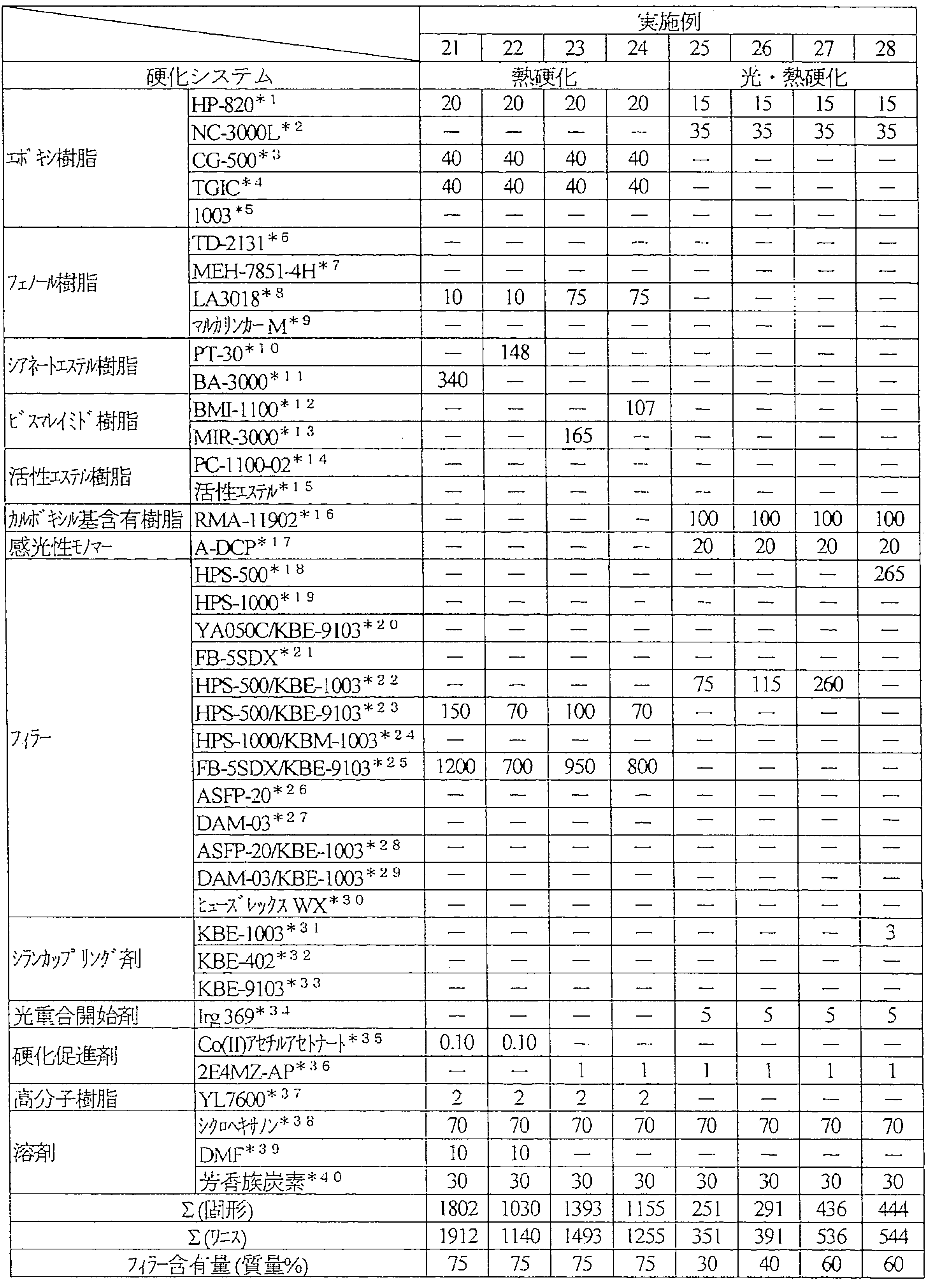


*43:DIC社製HP-4032、ナフタレン型半固形エポキシ樹脂、エポキシ当量:150g/eq
*44:DIC社製N-740、フェノールノボラック型半固形エポキシ樹脂、エポキシ当量:180g/eq
* 43: DIC's HP-4032, naphthalene type semi-solid epoxy resin, epoxy equivalent: 150 g / eq
* 44: N-740 manufactured by DIC, phenol novolac semi-solid epoxy resin, epoxy equivalent: 180 g / eq


*46:石原産業製タイペークCR-97 D50=0.25μm
*47:堺化学工業製CZ-03 D50=0.3μm
* 46: Ishihara Sangyo Typepek CR-97 D50 = 0.25μm
* 47: Sakai Chemical Industry CZ-03 D50 = 0.3 μm


12 樹脂層
13 フィルム
21 三層構造のドライフィルム
22 樹脂層
23 第一のフィルム
24 第二のフィルム
30a 液状判定用試験管
30b 温度測定用試験管
31 標線(A線)
32 標線(B線)
33a、33b ゴム栓
34 温度計
DESCRIPTION OF SYMBOLS 11 Two-layer
32 Mark (B line)
33a,
Claims (9)
- フィルムと、該フィルム上に形成したエポキシ樹脂を含む樹脂層と、を有するドライフィルムであって、
前記樹脂層の溶融粘度が、100℃で60~5500dPa・sであり、
前記樹脂層の貯蔵弾性率が、100℃で80~5500Paであり、
前記樹脂層が、前記エポキシ樹脂として、少なくとも液状エポキシ樹脂を含み、
前記液状エポキシ樹脂の含有量が、前記エポキシ樹脂全質量あたり60質量%未満であることを特徴とするドライフィルム。 A dry film having a film and a resin layer containing an epoxy resin formed on the film,
The resin layer has a melt viscosity of 60 to 5500 dPa · s at 100 ° C.,
The storage elastic modulus of the resin layer is 80 to 5500 Pa at 100 ° C.,
The resin layer includes at least a liquid epoxy resin as the epoxy resin,
Content of the said liquid epoxy resin is less than 60 mass% per said epoxy resin total mass, The dry film characterized by the above-mentioned. - 前記樹脂層中の残留溶剤量が、1.0~7.0質量%である請求項1記載のドライフィルム。 The dry film according to claim 1, wherein the amount of residual solvent in the resin layer is 1.0 to 7.0% by mass.
- 前記樹脂層中に、N,N-ジメチルホルムアミド、トルエン、シクロヘキサノン、炭素数が8以上の芳香族炭化水素およびメチルエチルケトンからなる群より選ばれる少なくとも2種の有機溶剤を含むことを特徴とする請求項1記載のドライフィルム。 The resin layer contains at least two organic solvents selected from the group consisting of N, N-dimethylformamide, toluene, cyclohexanone, aromatic hydrocarbons having 8 or more carbon atoms, and methyl ethyl ketone. 1. The dry film according to 1.
- 前記樹脂層が、前記エポキシ樹脂として、さらに、ビスフェノールA型エポキシ樹脂、ナフタレン型エポキシ樹脂およびフェノールノボラック型エポキシ樹脂からなる群より選ばれる少なくとも1種の半固形エポキシ樹脂を含むことを特徴とする請求項1記載のドライフィルム。 The resin layer further includes at least one semi-solid epoxy resin selected from the group consisting of a bisphenol A type epoxy resin, a naphthalene type epoxy resin, and a phenol novolac type epoxy resin as the epoxy resin. Item 2. The dry film according to Item 1.
- 前記樹脂層が、フィラーを含み、
前記フィラーの平均粒径が、0.1~10μmである請求項1記載のドライフィルム。 The resin layer includes a filler,
2. The dry film according to claim 1, wherein the filler has an average particle size of 0.1 to 10 μm. - 前記樹脂層が、フィラーを含み、
前記フィラーの配合量が、樹脂層全量(樹脂層が溶剤を含む場合は溶剤を除く全量)あたり40~80質量%である請求項1記載のドライフィルム。 The resin layer includes a filler,
The dry film according to claim 1, wherein the blending amount of the filler is 40 to 80% by mass based on the total amount of the resin layer (the total amount excluding the solvent when the resin layer includes a solvent). - 前記樹脂層が、フィラーを含み、
前記フィラーが、エポキシ基を有するシランカップリング剤、アミノ基を有するシランカップリング剤、メルカプト基を有するシランカップリング剤、イソシアネート基を有するシランカップリング剤、ビニル基を有するシランカップリング剤、スチリル基を有するシランカップリング剤、メタクリル基を有するシランカップリング剤およびアクリル基を有するシランカップリング剤の少なくともいずれか1種で表面処理されている請求項1記載のドライフィルム。 The resin layer includes a filler,
The filler is an epoxy group-containing silane coupling agent, an amino group-containing silane coupling agent, a mercapto group-containing silane coupling agent, an isocyanate group-containing silane coupling agent, a vinyl group-containing silane coupling agent, or styryl. The dry film according to claim 1, which is surface-treated with at least one of a silane coupling agent having a group, a silane coupling agent having a methacryl group, and a silane coupling agent having an acrylic group. - 請求項1~7のいずれか一項記載のドライフィルムの樹脂層を硬化して得られることを特徴とする硬化物。 A cured product obtained by curing the resin layer of the dry film according to any one of claims 1 to 7.
- 請求項8記載の硬化物を具備することを特徴とするプリント配線板。 A printed wiring board comprising the cured product according to claim 8.
Priority Applications (3)
| Application Number | Priority Date | Filing Date | Title |
|---|---|---|---|
| CN201680078987.6A CN108476589B (en) | 2016-01-13 | 2016-12-06 | Dry film and printed circuit board |
| KR1020187022984A KR102641274B1 (en) | 2016-01-13 | 2016-12-06 | Dry film and printed wiring board |
| JP2017561542A JP6937701B2 (en) | 2016-01-13 | 2016-12-06 | Dry film and printed wiring board |
Applications Claiming Priority (2)
| Application Number | Priority Date | Filing Date | Title |
|---|---|---|---|
| JP2016004825 | 2016-01-13 | ||
| JP2016-004825 | 2016-01-13 |
Publications (1)
| Publication Number | Publication Date |
|---|---|
| WO2017122460A1 true WO2017122460A1 (en) | 2017-07-20 |
Family
ID=59311203
Family Applications (1)
| Application Number | Title | Priority Date | Filing Date |
|---|---|---|---|
| PCT/JP2016/086192 WO2017122460A1 (en) | 2016-01-13 | 2016-12-06 | Dry film and printed wiring board |
Country Status (5)
| Country | Link |
|---|---|
| JP (1) | JP6937701B2 (en) |
| KR (1) | KR102641274B1 (en) |
| CN (1) | CN108476589B (en) |
| TW (1) | TWI721070B (en) |
| WO (1) | WO2017122460A1 (en) |
Cited By (15)
| Publication number | Priority date | Publication date | Assignee | Title |
|---|---|---|---|---|
| JP2018053092A (en) * | 2016-09-28 | 2018-04-05 | 味の素株式会社 | Resin composition |
| WO2018123695A1 (en) * | 2016-12-28 | 2018-07-05 | 太陽インキ製造株式会社 | Curable composition, base resin, curing agent, dry film, cured product, and printed wiring board |
| JP2019044006A (en) * | 2017-08-30 | 2019-03-22 | 京セラ株式会社 | Resin composition for semiconductor sealing and semiconductor device |
| WO2019138992A1 (en) * | 2018-01-09 | 2019-07-18 | 三菱瓦斯化学株式会社 | Resin composition, prepreg, metal-foil-lined laminate, resin composite sheet, and printed circuit board |
| WO2019176859A1 (en) * | 2018-03-16 | 2019-09-19 | 日立化成株式会社 | Epoxy resin composition and electronic component device |
| WO2019187904A1 (en) * | 2018-03-30 | 2019-10-03 | 太陽インキ製造株式会社 | Alkali developing-type photosensitive resin composition, dry film, cured product and printed circuit board |
| WO2020040092A1 (en) * | 2018-08-20 | 2020-02-27 | Jsr株式会社 | Method for forming pattern, and radiation-sensitive composition |
| JP2020122158A (en) * | 2020-04-30 | 2020-08-13 | 味の素株式会社 | Resin composition |
| JP2020145270A (en) * | 2019-03-05 | 2020-09-10 | 住友ベークライト株式会社 | Electronic device |
| JP2020154052A (en) * | 2019-03-18 | 2020-09-24 | 太陽インキ製造株式会社 | Curable resin composition, dry film, cured product and electronic component |
| JP2020197603A (en) * | 2019-05-31 | 2020-12-10 | 昭和電工マテリアルズ株式会社 | Photosensitive resin composition, photosensitive resin film, multilayer printed wiring board, semiconductor package, and method of manufacturing multilayer printed wiring board |
| EP3901699A4 (en) * | 2018-12-19 | 2022-09-21 | Taiyo Ink Mfg. Co., Ltd. | Curable resin composition, dry film, cured article, and electronic component |
| WO2022202661A1 (en) * | 2021-03-25 | 2022-09-29 | 太陽インキ製造株式会社 | Laminate structure, cured product of resin layer in said laminate structure, electronic component, and cured product formation method |
| WO2023145974A1 (en) * | 2022-01-31 | 2023-08-03 | 太陽ホールディングス株式会社 | Film laminate, cured product, and printed wiring board comprising said cured product |
| WO2023238732A1 (en) * | 2022-06-06 | 2023-12-14 | 太陽ホールディングス株式会社 | Layered structure, cured product of resin layer in said layered structure, and electronic component having said cured product |
Families Citing this family (4)
| Publication number | Priority date | Publication date | Assignee | Title |
|---|---|---|---|---|
| KR102476086B1 (en) * | 2015-06-25 | 2022-12-09 | 닛뽄 가야쿠 가부시키가이샤 | Epoxy resin composition and cured product thereof |
| CN111378252A (en) * | 2018-12-29 | 2020-07-07 | 太阳油墨(苏州)有限公司 | Resin filler |
| JP7221064B2 (en) * | 2019-01-30 | 2023-02-13 | 太陽インキ製造株式会社 | Dry films, cured products and electronic components |
| KR102465161B1 (en) * | 2019-11-06 | 2022-11-09 | 주식회사 아모그린텍 | Heat radiation sheet, method for manufacturing thereof, and electronic device comprising the same |
Citations (5)
| Publication number | Priority date | Publication date | Assignee | Title |
|---|---|---|---|---|
| JP2005264109A (en) * | 2004-03-22 | 2005-09-29 | Hitachi Chem Co Ltd | Film-shaped adhesive and manufacturing method of semiconductor device using the same |
| JP2009227992A (en) * | 2008-02-29 | 2009-10-08 | Sekisui Chem Co Ltd | Film and printed circuit board |
| JP2015056480A (en) * | 2013-09-11 | 2015-03-23 | デクセリアルズ株式会社 | Underfill material, and method for manufacturing semiconductor device using the same |
| JP2015179829A (en) * | 2014-02-26 | 2015-10-08 | 日東電工株式会社 | Method of manufacturing electronic component package |
| JP2015216317A (en) * | 2014-05-13 | 2015-12-03 | 日東電工株式会社 | Method for manufacturing semiconductor device |
Family Cites Families (9)
| Publication number | Priority date | Publication date | Assignee | Title |
|---|---|---|---|---|
| JPH0715119A (en) | 1993-06-23 | 1995-01-17 | Toagosei Co Ltd | Dry film type solder resist |
| JP2002162736A (en) | 2000-11-22 | 2002-06-07 | Kanegafuchi Chem Ind Co Ltd | Photosensitive dry film |
| JP2003131366A (en) | 2001-10-30 | 2003-05-09 | Kansai Paint Co Ltd | Positive active energy ray-sensitive dry film |
| JPWO2008087890A1 (en) * | 2007-01-15 | 2010-05-06 | 太陽インキ製造株式会社 | Thermosetting resin composition |
| JP5150381B2 (en) * | 2008-06-20 | 2013-02-20 | 太陽ホールディングス株式会社 | Thermosetting resin composition |
| JP5251806B2 (en) * | 2009-09-24 | 2013-07-31 | 宇部興産株式会社 | Process for producing conjugated diene polymer |
| JP5810763B2 (en) * | 2011-09-02 | 2015-11-11 | 宇部興産株式会社 | Rubber composition |
| CN105917462B (en) * | 2013-11-28 | 2019-10-15 | 日东电工株式会社 | The manufacturing method of thermosetting encapsulation resin sheet and hollow package body |
| JPWO2015141797A1 (en) * | 2014-03-20 | 2017-04-13 | 日立化成株式会社 | Resin composition, resin sheet, resin sheet cured product, resin sheet laminate, resin sheet laminate cured product and method for producing the same, semiconductor device, and LED device |
-
2016
- 2016-12-06 CN CN201680078987.6A patent/CN108476589B/en active Active
- 2016-12-06 JP JP2017561542A patent/JP6937701B2/en active Active
- 2016-12-06 KR KR1020187022984A patent/KR102641274B1/en active IP Right Grant
- 2016-12-06 WO PCT/JP2016/086192 patent/WO2017122460A1/en active Application Filing
- 2016-12-14 TW TW105141431A patent/TWI721070B/en active
Patent Citations (5)
| Publication number | Priority date | Publication date | Assignee | Title |
|---|---|---|---|---|
| JP2005264109A (en) * | 2004-03-22 | 2005-09-29 | Hitachi Chem Co Ltd | Film-shaped adhesive and manufacturing method of semiconductor device using the same |
| JP2009227992A (en) * | 2008-02-29 | 2009-10-08 | Sekisui Chem Co Ltd | Film and printed circuit board |
| JP2015056480A (en) * | 2013-09-11 | 2015-03-23 | デクセリアルズ株式会社 | Underfill material, and method for manufacturing semiconductor device using the same |
| JP2015179829A (en) * | 2014-02-26 | 2015-10-08 | 日東電工株式会社 | Method of manufacturing electronic component package |
| JP2015216317A (en) * | 2014-05-13 | 2015-12-03 | 日東電工株式会社 | Method for manufacturing semiconductor device |
Cited By (28)
| Publication number | Priority date | Publication date | Assignee | Title |
|---|---|---|---|---|
| JP2018053092A (en) * | 2016-09-28 | 2018-04-05 | 味の素株式会社 | Resin composition |
| JP7102093B2 (en) | 2016-09-28 | 2022-07-19 | 味の素株式会社 | Resin composition, resin sheet, circuit board and semiconductor chip package |
| WO2018123695A1 (en) * | 2016-12-28 | 2018-07-05 | 太陽インキ製造株式会社 | Curable composition, base resin, curing agent, dry film, cured product, and printed wiring board |
| JP2019044006A (en) * | 2017-08-30 | 2019-03-22 | 京セラ株式会社 | Resin composition for semiconductor sealing and semiconductor device |
| JPWO2019138992A1 (en) * | 2018-01-09 | 2020-01-16 | 三菱瓦斯化学株式会社 | Resin composition, prepreg, metal foil-clad laminate, resin composite sheet, and printed wiring board |
| CN111386313A (en) * | 2018-01-09 | 2020-07-07 | 三菱瓦斯化学株式会社 | Resin composition, prepreg, metal foil-clad laminate, resin composite sheet, and printed wiring board |
| WO2019138992A1 (en) * | 2018-01-09 | 2019-07-18 | 三菱瓦斯化学株式会社 | Resin composition, prepreg, metal-foil-lined laminate, resin composite sheet, and printed circuit board |
| US11008420B2 (en) | 2018-01-09 | 2021-05-18 | Mitsubishi Gas Chemical Company, Inc. | Resin composition, prepreg, metal foil-clad laminate, resin composite sheet, and printed wiring board |
| CN111386313B (en) * | 2018-01-09 | 2020-10-30 | 三菱瓦斯化学株式会社 | Resin composition, prepreg, metal foil-clad laminate, resin composite sheet, and printed wiring board |
| CN111868169B (en) * | 2018-03-16 | 2024-03-08 | 株式会社力森诺科 | Epoxy resin composition and electronic component device |
| CN111868169A (en) * | 2018-03-16 | 2020-10-30 | 日立化成株式会社 | Epoxy resin composition and electronic component device |
| WO2019176859A1 (en) * | 2018-03-16 | 2019-09-19 | 日立化成株式会社 | Epoxy resin composition and electronic component device |
| JP7351291B2 (en) | 2018-03-16 | 2023-09-27 | 株式会社レゾナック | Epoxy resin composition and electronic component equipment |
| JPWO2019176859A1 (en) * | 2018-03-16 | 2021-03-11 | 昭和電工マテリアルズ株式会社 | Epoxy resin composition and electronic component equipment |
| CN110753881A (en) * | 2018-03-30 | 2020-02-04 | 太阳油墨制造株式会社 | Alkali development type photosensitive resin composition, dry film, cured product and printed wiring board |
| WO2019187904A1 (en) * | 2018-03-30 | 2019-10-03 | 太陽インキ製造株式会社 | Alkali developing-type photosensitive resin composition, dry film, cured product and printed circuit board |
| WO2020040092A1 (en) * | 2018-08-20 | 2020-02-27 | Jsr株式会社 | Method for forming pattern, and radiation-sensitive composition |
| EP3901699A4 (en) * | 2018-12-19 | 2022-09-21 | Taiyo Ink Mfg. Co., Ltd. | Curable resin composition, dry film, cured article, and electronic component |
| JP2020145270A (en) * | 2019-03-05 | 2020-09-10 | 住友ベークライト株式会社 | Electronic device |
| JP2020154052A (en) * | 2019-03-18 | 2020-09-24 | 太陽インキ製造株式会社 | Curable resin composition, dry film, cured product and electronic component |
| JP7316071B2 (en) | 2019-03-18 | 2023-07-27 | 太陽ホールディングス株式会社 | Curable resin compositions, dry films, cured products and electronic components |
| JP2020197603A (en) * | 2019-05-31 | 2020-12-10 | 昭和電工マテリアルズ株式会社 | Photosensitive resin composition, photosensitive resin film, multilayer printed wiring board, semiconductor package, and method of manufacturing multilayer printed wiring board |
| JP7251323B2 (en) | 2019-05-31 | 2023-04-04 | 株式会社レゾナック | Photosensitive resin composition, photosensitive resin film, multilayer printed wiring board, semiconductor package, and method for producing multilayer printed wiring board |
| JP7070604B2 (en) | 2020-04-30 | 2022-05-18 | 味の素株式会社 | Resin composition, resin sheet, circuit board and semiconductor chip package |
| JP2020122158A (en) * | 2020-04-30 | 2020-08-13 | 味の素株式会社 | Resin composition |
| WO2022202661A1 (en) * | 2021-03-25 | 2022-09-29 | 太陽インキ製造株式会社 | Laminate structure, cured product of resin layer in said laminate structure, electronic component, and cured product formation method |
| WO2023145974A1 (en) * | 2022-01-31 | 2023-08-03 | 太陽ホールディングス株式会社 | Film laminate, cured product, and printed wiring board comprising said cured product |
| WO2023238732A1 (en) * | 2022-06-06 | 2023-12-14 | 太陽ホールディングス株式会社 | Layered structure, cured product of resin layer in said layered structure, and electronic component having said cured product |
Also Published As
| Publication number | Publication date |
|---|---|
| JP6937701B2 (en) | 2021-09-22 |
| KR20180103101A (en) | 2018-09-18 |
| TW201801584A (en) | 2018-01-01 |
| JPWO2017122460A1 (en) | 2018-11-01 |
| TWI721070B (en) | 2021-03-11 |
| CN108476589A (en) | 2018-08-31 |
| KR102641274B1 (en) | 2024-02-29 |
| CN108476589B (en) | 2021-10-26 |
Similar Documents
| Publication | Publication Date | Title |
|---|---|---|
| WO2017122460A1 (en) | Dry film and printed wiring board | |
| JP6294360B2 (en) | Photocurable and thermosetting resin composition and dry film solder resist | |
| TWI745366B (en) | Curable resin composition, dry film, cured product, and printed wiring board | |
| JP2016086000A (en) | Dry film and printed wiring board | |
| JP2016079384A (en) | Dry film, cured product, and printed wiring board | |
| JP2019166688A (en) | Dry film, cured product and electronic component | |
| JP2019178307A (en) | Curable resin composition, dry film, cured product and electronic component | |
| TW201842407A (en) | Photosensitive resin composition obtaining a cured product high glass transition temperature and excellent undercut resistance and crack resistance | |
| JP6710034B2 (en) | Curable resin composition, dry film, cured product and printed wiring board | |
| JP2018173609A (en) | Curable resin composition, dry film, cured product, and printed wiring board | |
| KR102543357B1 (en) | Laminated film | |
| US20230047699A1 (en) | Photosensitive resin composition, photosensitive resin film, multilayered printed wiring board, semiconductor package, and method for producing multilayered printed wiring board | |
| US20230303750A1 (en) | Photosensitive resin composition, photosensitive resin film, multilayered printed wiring board, semiconductor package, and method for producing multilayered printed wiring board | |
| JP6837281B2 (en) | Laminated film | |
| JP7388374B2 (en) | Photosensitive resin composition | |
| JP2019178303A (en) | Curable resin composition, dry film, cured product and electronic component | |
| JP2019178306A (en) | Curable resin composition, dry film, cured product and electronic component | |
| JP7444192B2 (en) | Photosensitive resin composition | |
| KR102543365B1 (en) | Curable composition, dry film, cured product and printed wiring board | |
| JP7445095B2 (en) | Photosensitive resin compositions, dry films, cured products, and printed wiring boards | |
| JP6742796B2 (en) | Curable resin composition, dry film, cured product and printed wiring board | |
| WO2023190393A1 (en) | Cured product and printed wiring board | |
| KR101746788B1 (en) | Multifunctional compound, photo-curable and thermo-curable resin composition and dry film solder resist | |
| KR20240054181A (en) | Photosensitive resin composition, dry film, cured product, and printed wiring board | |
| JP2024059604A (en) | Photosensitive resin composition, dry film, cured product, and printed wiring board |
Legal Events
| Date | Code | Title | Description |
|---|---|---|---|
| 121 | Ep: the epo has been informed by wipo that ep was designated in this application |
Ref document number: 16885063 Country of ref document: EP Kind code of ref document: A1 |
|
| ENP | Entry into the national phase |
Ref document number: 2017561542 Country of ref document: JP Kind code of ref document: A |
|
| NENP | Non-entry into the national phase |
Ref country code: DE |
|
| ENP | Entry into the national phase |
Ref document number: 20187022984 Country of ref document: KR Kind code of ref document: A |
|
| WWE | Wipo information: entry into national phase |
Ref document number: 1020187022984 Country of ref document: KR |
|
| 122 | Ep: pct application non-entry in european phase |
Ref document number: 16885063 Country of ref document: EP Kind code of ref document: A1 |