WO2017115803A1 - 液晶積層体、および、液晶積層体の製造方法 - Google Patents
液晶積層体、および、液晶積層体の製造方法 Download PDFInfo
- Publication number
- WO2017115803A1 WO2017115803A1 PCT/JP2016/088920 JP2016088920W WO2017115803A1 WO 2017115803 A1 WO2017115803 A1 WO 2017115803A1 JP 2016088920 W JP2016088920 W JP 2016088920W WO 2017115803 A1 WO2017115803 A1 WO 2017115803A1
- Authority
- WO
- WIPO (PCT)
- Prior art keywords
- layer
- liquid crystal
- adhesive layer
- base material
- substrate
- Prior art date
- Legal status (The legal status is an assumption and is not a legal conclusion. Google has not performed a legal analysis and makes no representation as to the accuracy of the status listed.)
- Ceased
Links
Images






Classifications
-
- B—PERFORMING OPERATIONS; TRANSPORTING
- B32—LAYERED PRODUCTS
- B32B—LAYERED PRODUCTS, i.e. PRODUCTS BUILT-UP OF STRATA OF FLAT OR NON-FLAT, e.g. CELLULAR OR HONEYCOMB, FORM
- B32B27/00—Layered products comprising a layer of synthetic resin
- B32B27/36—Layered products comprising a layer of synthetic resin comprising polyesters
- B32B27/365—Layered products comprising a layer of synthetic resin comprising polyesters comprising polycarbonates
-
- B—PERFORMING OPERATIONS; TRANSPORTING
- B32—LAYERED PRODUCTS
- B32B—LAYERED PRODUCTS, i.e. PRODUCTS BUILT-UP OF STRATA OF FLAT OR NON-FLAT, e.g. CELLULAR OR HONEYCOMB, FORM
- B32B15/00—Layered products comprising a layer of metal
- B32B15/04—Layered products comprising a layer of metal comprising metal as the main or only constituent of a layer, which is next to another layer of the same or of a different material
- B32B15/08—Layered products comprising a layer of metal comprising metal as the main or only constituent of a layer, which is next to another layer of the same or of a different material of synthetic resin
- B32B15/085—Layered products comprising a layer of metal comprising metal as the main or only constituent of a layer, which is next to another layer of the same or of a different material of synthetic resin comprising polyolefins
-
- B—PERFORMING OPERATIONS; TRANSPORTING
- B32—LAYERED PRODUCTS
- B32B—LAYERED PRODUCTS, i.e. PRODUCTS BUILT-UP OF STRATA OF FLAT OR NON-FLAT, e.g. CELLULAR OR HONEYCOMB, FORM
- B32B15/00—Layered products comprising a layer of metal
- B32B15/04—Layered products comprising a layer of metal comprising metal as the main or only constituent of a layer, which is next to another layer of the same or of a different material
- B32B15/08—Layered products comprising a layer of metal comprising metal as the main or only constituent of a layer, which is next to another layer of the same or of a different material of synthetic resin
- B32B15/082—Layered products comprising a layer of metal comprising metal as the main or only constituent of a layer, which is next to another layer of the same or of a different material of synthetic resin comprising vinyl resins; comprising acrylic resins
-
- B—PERFORMING OPERATIONS; TRANSPORTING
- B32—LAYERED PRODUCTS
- B32B—LAYERED PRODUCTS, i.e. PRODUCTS BUILT-UP OF STRATA OF FLAT OR NON-FLAT, e.g. CELLULAR OR HONEYCOMB, FORM
- B32B23/00—Layered products comprising a layer of cellulosic plastic substances, i.e. substances obtained by chemical modification of cellulose, e.g. cellulose ethers, cellulose esters, viscose
- B32B23/04—Layered products comprising a layer of cellulosic plastic substances, i.e. substances obtained by chemical modification of cellulose, e.g. cellulose ethers, cellulose esters, viscose comprising such cellulosic plastic substance as the main or only constituent of a layer, which is next to another layer of the same or of a different material
- B32B23/08—Layered products comprising a layer of cellulosic plastic substances, i.e. substances obtained by chemical modification of cellulose, e.g. cellulose ethers, cellulose esters, viscose comprising such cellulosic plastic substance as the main or only constituent of a layer, which is next to another layer of the same or of a different material of synthetic resin
-
- B—PERFORMING OPERATIONS; TRANSPORTING
- B32—LAYERED PRODUCTS
- B32B—LAYERED PRODUCTS, i.e. PRODUCTS BUILT-UP OF STRATA OF FLAT OR NON-FLAT, e.g. CELLULAR OR HONEYCOMB, FORM
- B32B27/00—Layered products comprising a layer of synthetic resin
- B32B27/06—Layered products comprising a layer of synthetic resin as the main or only constituent of a layer, which is next to another layer of the same or of a different material
- B32B27/08—Layered products comprising a layer of synthetic resin as the main or only constituent of a layer, which is next to another layer of the same or of a different material of synthetic resin
-
- B—PERFORMING OPERATIONS; TRANSPORTING
- B32—LAYERED PRODUCTS
- B32B—LAYERED PRODUCTS, i.e. PRODUCTS BUILT-UP OF STRATA OF FLAT OR NON-FLAT, e.g. CELLULAR OR HONEYCOMB, FORM
- B32B27/00—Layered products comprising a layer of synthetic resin
- B32B27/30—Layered products comprising a layer of synthetic resin comprising vinyl (co)polymers; comprising acrylic (co)polymers
- B32B27/302—Layered products comprising a layer of synthetic resin comprising vinyl (co)polymers; comprising acrylic (co)polymers comprising aromatic vinyl (co)polymers, e.g. styrenic (co)polymers
-
- B—PERFORMING OPERATIONS; TRANSPORTING
- B32—LAYERED PRODUCTS
- B32B—LAYERED PRODUCTS, i.e. PRODUCTS BUILT-UP OF STRATA OF FLAT OR NON-FLAT, e.g. CELLULAR OR HONEYCOMB, FORM
- B32B27/00—Layered products comprising a layer of synthetic resin
- B32B27/30—Layered products comprising a layer of synthetic resin comprising vinyl (co)polymers; comprising acrylic (co)polymers
- B32B27/304—Layered products comprising a layer of synthetic resin comprising vinyl (co)polymers; comprising acrylic (co)polymers comprising vinyl halide (co)polymers, e.g. PVC, PVDC, PVF, PVDF
-
- B—PERFORMING OPERATIONS; TRANSPORTING
- B32—LAYERED PRODUCTS
- B32B—LAYERED PRODUCTS, i.e. PRODUCTS BUILT-UP OF STRATA OF FLAT OR NON-FLAT, e.g. CELLULAR OR HONEYCOMB, FORM
- B32B27/00—Layered products comprising a layer of synthetic resin
- B32B27/30—Layered products comprising a layer of synthetic resin comprising vinyl (co)polymers; comprising acrylic (co)polymers
- B32B27/306—Layered products comprising a layer of synthetic resin comprising vinyl (co)polymers; comprising acrylic (co)polymers comprising vinyl acetate or vinyl alcohol (co)polymers
-
- B—PERFORMING OPERATIONS; TRANSPORTING
- B32—LAYERED PRODUCTS
- B32B—LAYERED PRODUCTS, i.e. PRODUCTS BUILT-UP OF STRATA OF FLAT OR NON-FLAT, e.g. CELLULAR OR HONEYCOMB, FORM
- B32B27/00—Layered products comprising a layer of synthetic resin
- B32B27/30—Layered products comprising a layer of synthetic resin comprising vinyl (co)polymers; comprising acrylic (co)polymers
- B32B27/308—Layered products comprising a layer of synthetic resin comprising vinyl (co)polymers; comprising acrylic (co)polymers comprising acrylic (co)polymers
-
- B—PERFORMING OPERATIONS; TRANSPORTING
- B32—LAYERED PRODUCTS
- B32B—LAYERED PRODUCTS, i.e. PRODUCTS BUILT-UP OF STRATA OF FLAT OR NON-FLAT, e.g. CELLULAR OR HONEYCOMB, FORM
- B32B27/00—Layered products comprising a layer of synthetic resin
- B32B27/32—Layered products comprising a layer of synthetic resin comprising polyolefins
-
- B—PERFORMING OPERATIONS; TRANSPORTING
- B32—LAYERED PRODUCTS
- B32B—LAYERED PRODUCTS, i.e. PRODUCTS BUILT-UP OF STRATA OF FLAT OR NON-FLAT, e.g. CELLULAR OR HONEYCOMB, FORM
- B32B27/00—Layered products comprising a layer of synthetic resin
- B32B27/34—Layered products comprising a layer of synthetic resin comprising polyamides
-
- B—PERFORMING OPERATIONS; TRANSPORTING
- B32—LAYERED PRODUCTS
- B32B—LAYERED PRODUCTS, i.e. PRODUCTS BUILT-UP OF STRATA OF FLAT OR NON-FLAT, e.g. CELLULAR OR HONEYCOMB, FORM
- B32B27/00—Layered products comprising a layer of synthetic resin
- B32B27/36—Layered products comprising a layer of synthetic resin comprising polyesters
-
- B—PERFORMING OPERATIONS; TRANSPORTING
- B32—LAYERED PRODUCTS
- B32B—LAYERED PRODUCTS, i.e. PRODUCTS BUILT-UP OF STRATA OF FLAT OR NON-FLAT, e.g. CELLULAR OR HONEYCOMB, FORM
- B32B29/00—Layered products comprising a layer of paper or cardboard
- B32B29/002—Layered products comprising a layer of paper or cardboard as the main or only constituent of a layer, which is next to another layer of the same or of a different material
- B32B29/005—Layered products comprising a layer of paper or cardboard as the main or only constituent of a layer, which is next to another layer of the same or of a different material next to another layer of paper or cardboard layer
-
- B—PERFORMING OPERATIONS; TRANSPORTING
- B32—LAYERED PRODUCTS
- B32B—LAYERED PRODUCTS, i.e. PRODUCTS BUILT-UP OF STRATA OF FLAT OR NON-FLAT, e.g. CELLULAR OR HONEYCOMB, FORM
- B32B7/00—Layered products characterised by the relation between layers; Layered products characterised by the relative orientation of features between layers, or by the relative values of a measurable parameter between layers, i.e. products comprising layers having different physical, chemical or physicochemical properties; Layered products characterised by the interconnection of layers
- B32B7/04—Interconnection of layers
- B32B7/06—Interconnection of layers permitting easy separation
-
- B—PERFORMING OPERATIONS; TRANSPORTING
- B32—LAYERED PRODUCTS
- B32B—LAYERED PRODUCTS, i.e. PRODUCTS BUILT-UP OF STRATA OF FLAT OR NON-FLAT, e.g. CELLULAR OR HONEYCOMB, FORM
- B32B7/00—Layered products characterised by the relation between layers; Layered products characterised by the relative orientation of features between layers, or by the relative values of a measurable parameter between layers, i.e. products comprising layers having different physical, chemical or physicochemical properties; Layered products characterised by the interconnection of layers
- B32B7/04—Interconnection of layers
- B32B7/12—Interconnection of layers using interposed adhesives or interposed materials with bonding properties
-
- B—PERFORMING OPERATIONS; TRANSPORTING
- B42—BOOKBINDING; ALBUMS; FILES; SPECIAL PRINTED MATTER
- B42D—BOOKS; BOOK COVERS; LOOSE LEAVES; PRINTED MATTER CHARACTERISED BY IDENTIFICATION OR SECURITY FEATURES; PRINTED MATTER OF SPECIAL FORMAT OR STYLE NOT OTHERWISE PROVIDED FOR; DEVICES FOR USE THEREWITH AND NOT OTHERWISE PROVIDED FOR; MOVABLE-STRIP WRITING OR READING APPARATUS
- B42D25/00—Information-bearing cards or sheet-like structures characterised by identification or security features; Manufacture thereof
- B42D25/30—Identification or security features, e.g. for preventing forgery
- B42D25/328—Diffraction gratings; Holograms
-
- B—PERFORMING OPERATIONS; TRANSPORTING
- B42—BOOKBINDING; ALBUMS; FILES; SPECIAL PRINTED MATTER
- B42D—BOOKS; BOOK COVERS; LOOSE LEAVES; PRINTED MATTER CHARACTERISED BY IDENTIFICATION OR SECURITY FEATURES; PRINTED MATTER OF SPECIAL FORMAT OR STYLE NOT OTHERWISE PROVIDED FOR; DEVICES FOR USE THEREWITH AND NOT OTHERWISE PROVIDED FOR; MOVABLE-STRIP WRITING OR READING APPARATUS
- B42D25/00—Information-bearing cards or sheet-like structures characterised by identification or security features; Manufacture thereof
- B42D25/30—Identification or security features, e.g. for preventing forgery
- B42D25/36—Identification or security features, e.g. for preventing forgery comprising special materials
- B42D25/364—Liquid crystals
-
- B—PERFORMING OPERATIONS; TRANSPORTING
- B42—BOOKBINDING; ALBUMS; FILES; SPECIAL PRINTED MATTER
- B42D—BOOKS; BOOK COVERS; LOOSE LEAVES; PRINTED MATTER CHARACTERISED BY IDENTIFICATION OR SECURITY FEATURES; PRINTED MATTER OF SPECIAL FORMAT OR STYLE NOT OTHERWISE PROVIDED FOR; DEVICES FOR USE THEREWITH AND NOT OTHERWISE PROVIDED FOR; MOVABLE-STRIP WRITING OR READING APPARATUS
- B42D25/00—Information-bearing cards or sheet-like structures characterised by identification or security features; Manufacture thereof
- B42D25/40—Manufacture
- B42D25/45—Associating two or more layers
-
- G—PHYSICS
- G02—OPTICS
- G02B—OPTICAL ELEMENTS, SYSTEMS OR APPARATUS
- G02B26/00—Optical devices or arrangements for the control of light using movable or deformable optical elements
- G02B26/06—Optical devices or arrangements for the control of light using movable or deformable optical elements for controlling the phase of light
-
- G—PHYSICS
- G02—OPTICS
- G02B—OPTICAL ELEMENTS, SYSTEMS OR APPARATUS
- G02B5/00—Optical elements other than lenses
- G02B5/18—Diffraction gratings
-
- G—PHYSICS
- G02—OPTICS
- G02B—OPTICAL ELEMENTS, SYSTEMS OR APPARATUS
- G02B5/00—Optical elements other than lenses
- G02B5/18—Diffraction gratings
- G02B5/1814—Diffraction gratings structurally combined with one or more further optical elements, e.g. lenses, mirrors, prisms or other diffraction gratings
-
- G—PHYSICS
- G03—PHOTOGRAPHY; CINEMATOGRAPHY; ANALOGOUS TECHNIQUES USING WAVES OTHER THAN OPTICAL WAVES; ELECTROGRAPHY; HOLOGRAPHY
- G03H—HOLOGRAPHIC PROCESSES OR APPARATUS
- G03H1/00—Holographic processes or apparatus using light, infrared or ultraviolet waves for obtaining holograms or for obtaining an image from them; Details peculiar thereto
- G03H1/0005—Adaptation of holography to specific applications
- G03H1/0011—Adaptation of holography to specific applications for security or authentication
-
- G—PHYSICS
- G03—PHOTOGRAPHY; CINEMATOGRAPHY; ANALOGOUS TECHNIQUES USING WAVES OTHER THAN OPTICAL WAVES; ELECTROGRAPHY; HOLOGRAPHY
- G03H—HOLOGRAPHIC PROCESSES OR APPARATUS
- G03H1/00—Holographic processes or apparatus using light, infrared or ultraviolet waves for obtaining holograms or for obtaining an image from them; Details peculiar thereto
- G03H1/02—Details of features involved during the holographic process; Replication of holograms without interference recording
- G03H1/024—Hologram nature or properties
- G03H1/0244—Surface relief holograms
-
- G—PHYSICS
- G03—PHOTOGRAPHY; CINEMATOGRAPHY; ANALOGOUS TECHNIQUES USING WAVES OTHER THAN OPTICAL WAVES; ELECTROGRAPHY; HOLOGRAPHY
- G03H—HOLOGRAPHIC PROCESSES OR APPARATUS
- G03H1/00—Holographic processes or apparatus using light, infrared or ultraviolet waves for obtaining holograms or for obtaining an image from them; Details peculiar thereto
- G03H1/02—Details of features involved during the holographic process; Replication of holograms without interference recording
- G03H1/024—Hologram nature or properties
- G03H1/0248—Volume holograms
-
- G—PHYSICS
- G03—PHOTOGRAPHY; CINEMATOGRAPHY; ANALOGOUS TECHNIQUES USING WAVES OTHER THAN OPTICAL WAVES; ELECTROGRAPHY; HOLOGRAPHY
- G03H—HOLOGRAPHIC PROCESSES OR APPARATUS
- G03H1/00—Holographic processes or apparatus using light, infrared or ultraviolet waves for obtaining holograms or for obtaining an image from them; Details peculiar thereto
- G03H1/02—Details of features involved during the holographic process; Replication of holograms without interference recording
- G03H1/0252—Laminate comprising a hologram layer
- G03H1/0256—Laminate comprising a hologram layer having specific functional layer
-
- G—PHYSICS
- G03—PHOTOGRAPHY; CINEMATOGRAPHY; ANALOGOUS TECHNIQUES USING WAVES OTHER THAN OPTICAL WAVES; ELECTROGRAPHY; HOLOGRAPHY
- G03H—HOLOGRAPHIC PROCESSES OR APPARATUS
- G03H1/00—Holographic processes or apparatus using light, infrared or ultraviolet waves for obtaining holograms or for obtaining an image from them; Details peculiar thereto
- G03H1/04—Processes or apparatus for producing holograms
- G03H1/18—Particular processing of hologram record carriers, e.g. for obtaining blazed holograms
- G03H1/182—Post-exposure processing, e.g. latensification
-
- B—PERFORMING OPERATIONS; TRANSPORTING
- B32—LAYERED PRODUCTS
- B32B—LAYERED PRODUCTS, i.e. PRODUCTS BUILT-UP OF STRATA OF FLAT OR NON-FLAT, e.g. CELLULAR OR HONEYCOMB, FORM
- B32B2255/00—Coating on the layer surface
- B32B2255/10—Coating on the layer surface on synthetic resin layer or on natural or synthetic rubber layer
-
- B—PERFORMING OPERATIONS; TRANSPORTING
- B32—LAYERED PRODUCTS
- B32B—LAYERED PRODUCTS, i.e. PRODUCTS BUILT-UP OF STRATA OF FLAT OR NON-FLAT, e.g. CELLULAR OR HONEYCOMB, FORM
- B32B2255/00—Coating on the layer surface
- B32B2255/12—Coating on the layer surface on paper layer
-
- B—PERFORMING OPERATIONS; TRANSPORTING
- B32—LAYERED PRODUCTS
- B32B—LAYERED PRODUCTS, i.e. PRODUCTS BUILT-UP OF STRATA OF FLAT OR NON-FLAT, e.g. CELLULAR OR HONEYCOMB, FORM
- B32B2255/00—Coating on the layer surface
- B32B2255/20—Inorganic coating
- B32B2255/205—Metallic coating
-
- B—PERFORMING OPERATIONS; TRANSPORTING
- B32—LAYERED PRODUCTS
- B32B—LAYERED PRODUCTS, i.e. PRODUCTS BUILT-UP OF STRATA OF FLAT OR NON-FLAT, e.g. CELLULAR OR HONEYCOMB, FORM
- B32B2255/00—Coating on the layer surface
- B32B2255/26—Polymeric coating
-
- B—PERFORMING OPERATIONS; TRANSPORTING
- B32—LAYERED PRODUCTS
- B32B—LAYERED PRODUCTS, i.e. PRODUCTS BUILT-UP OF STRATA OF FLAT OR NON-FLAT, e.g. CELLULAR OR HONEYCOMB, FORM
- B32B2255/00—Coating on the layer surface
- B32B2255/28—Multiple coating on one surface
-
- B—PERFORMING OPERATIONS; TRANSPORTING
- B32—LAYERED PRODUCTS
- B32B—LAYERED PRODUCTS, i.e. PRODUCTS BUILT-UP OF STRATA OF FLAT OR NON-FLAT, e.g. CELLULAR OR HONEYCOMB, FORM
- B32B2307/00—Properties of the layers or laminate
- B32B2307/40—Properties of the layers or laminate having particular optical properties
- B32B2307/402—Coloured
-
- B—PERFORMING OPERATIONS; TRANSPORTING
- B32—LAYERED PRODUCTS
- B32B—LAYERED PRODUCTS, i.e. PRODUCTS BUILT-UP OF STRATA OF FLAT OR NON-FLAT, e.g. CELLULAR OR HONEYCOMB, FORM
- B32B2307/00—Properties of the layers or laminate
- B32B2307/40—Properties of the layers or laminate having particular optical properties
- B32B2307/412—Transparent
-
- B—PERFORMING OPERATIONS; TRANSPORTING
- B32—LAYERED PRODUCTS
- B32B—LAYERED PRODUCTS, i.e. PRODUCTS BUILT-UP OF STRATA OF FLAT OR NON-FLAT, e.g. CELLULAR OR HONEYCOMB, FORM
- B32B2307/00—Properties of the layers or laminate
- B32B2307/50—Properties of the layers or laminate having particular mechanical properties
- B32B2307/514—Oriented
- B32B2307/516—Oriented mono-axially
-
- B—PERFORMING OPERATIONS; TRANSPORTING
- B32—LAYERED PRODUCTS
- B32B—LAYERED PRODUCTS, i.e. PRODUCTS BUILT-UP OF STRATA OF FLAT OR NON-FLAT, e.g. CELLULAR OR HONEYCOMB, FORM
- B32B2307/00—Properties of the layers or laminate
- B32B2307/50—Properties of the layers or laminate having particular mechanical properties
- B32B2307/514—Oriented
- B32B2307/518—Oriented bi-axially
-
- B—PERFORMING OPERATIONS; TRANSPORTING
- B32—LAYERED PRODUCTS
- B32B—LAYERED PRODUCTS, i.e. PRODUCTS BUILT-UP OF STRATA OF FLAT OR NON-FLAT, e.g. CELLULAR OR HONEYCOMB, FORM
- B32B2307/00—Properties of the layers or laminate
- B32B2307/50—Properties of the layers or laminate having particular mechanical properties
- B32B2307/546—Flexural strength; Flexion stiffness
-
- B—PERFORMING OPERATIONS; TRANSPORTING
- B32—LAYERED PRODUCTS
- B32B—LAYERED PRODUCTS, i.e. PRODUCTS BUILT-UP OF STRATA OF FLAT OR NON-FLAT, e.g. CELLULAR OR HONEYCOMB, FORM
- B32B2307/00—Properties of the layers or laminate
- B32B2307/50—Properties of the layers or laminate having particular mechanical properties
- B32B2307/554—Wear resistance
-
- B—PERFORMING OPERATIONS; TRANSPORTING
- B32—LAYERED PRODUCTS
- B32B—LAYERED PRODUCTS, i.e. PRODUCTS BUILT-UP OF STRATA OF FLAT OR NON-FLAT, e.g. CELLULAR OR HONEYCOMB, FORM
- B32B2307/00—Properties of the layers or laminate
- B32B2307/70—Other properties
- B32B2307/71—Resistive to light or to UV
-
- B—PERFORMING OPERATIONS; TRANSPORTING
- B32—LAYERED PRODUCTS
- B32B—LAYERED PRODUCTS, i.e. PRODUCTS BUILT-UP OF STRATA OF FLAT OR NON-FLAT, e.g. CELLULAR OR HONEYCOMB, FORM
- B32B2307/00—Properties of the layers or laminate
- B32B2307/70—Other properties
- B32B2307/732—Dimensional properties
-
- B—PERFORMING OPERATIONS; TRANSPORTING
- B32—LAYERED PRODUCTS
- B32B—LAYERED PRODUCTS, i.e. PRODUCTS BUILT-UP OF STRATA OF FLAT OR NON-FLAT, e.g. CELLULAR OR HONEYCOMB, FORM
- B32B2307/00—Properties of the layers or laminate
- B32B2307/70—Other properties
- B32B2307/748—Releasability
-
- B—PERFORMING OPERATIONS; TRANSPORTING
- B32—LAYERED PRODUCTS
- B32B—LAYERED PRODUCTS, i.e. PRODUCTS BUILT-UP OF STRATA OF FLAT OR NON-FLAT, e.g. CELLULAR OR HONEYCOMB, FORM
- B32B2457/00—Electrical equipment
- B32B2457/20—Displays, e.g. liquid crystal displays, plasma displays
-
- G—PHYSICS
- G03—PHOTOGRAPHY; CINEMATOGRAPHY; ANALOGOUS TECHNIQUES USING WAVES OTHER THAN OPTICAL WAVES; ELECTROGRAPHY; HOLOGRAPHY
- G03H—HOLOGRAPHIC PROCESSES OR APPARATUS
- G03H1/00—Holographic processes or apparatus using light, infrared or ultraviolet waves for obtaining holograms or for obtaining an image from them; Details peculiar thereto
- G03H1/04—Processes or apparatus for producing holograms
-
- G—PHYSICS
- G03—PHOTOGRAPHY; CINEMATOGRAPHY; ANALOGOUS TECHNIQUES USING WAVES OTHER THAN OPTICAL WAVES; ELECTROGRAPHY; HOLOGRAPHY
- G03H—HOLOGRAPHIC PROCESSES OR APPARATUS
- G03H1/00—Holographic processes or apparatus using light, infrared or ultraviolet waves for obtaining holograms or for obtaining an image from them; Details peculiar thereto
- G03H1/04—Processes or apparatus for producing holograms
- G03H1/18—Particular processing of hologram record carriers, e.g. for obtaining blazed holograms
- G03H2001/187—Trimming process, i.e. macroscopically patterning the hologram
- G03H2001/188—Demetallisation, i.e. removing the enhancing metallic layer
-
- G—PHYSICS
- G03—PHOTOGRAPHY; CINEMATOGRAPHY; ANALOGOUS TECHNIQUES USING WAVES OTHER THAN OPTICAL WAVES; ELECTROGRAPHY; HOLOGRAPHY
- G03H—HOLOGRAPHIC PROCESSES OR APPARATUS
- G03H2250/00—Laminate comprising a hologram layer
- G03H2250/36—Conform enhancement layer
-
- G—PHYSICS
- G03—PHOTOGRAPHY; CINEMATOGRAPHY; ANALOGOUS TECHNIQUES USING WAVES OTHER THAN OPTICAL WAVES; ELECTROGRAPHY; HOLOGRAPHY
- G03H—HOLOGRAPHIC PROCESSES OR APPARATUS
- G03H2250/00—Laminate comprising a hologram layer
- G03H2250/38—Liquid crystal
-
- G—PHYSICS
- G03—PHOTOGRAPHY; CINEMATOGRAPHY; ANALOGOUS TECHNIQUES USING WAVES OTHER THAN OPTICAL WAVES; ELECTROGRAPHY; HOLOGRAPHY
- G03H—HOLOGRAPHIC PROCESSES OR APPARATUS
- G03H2250/00—Laminate comprising a hologram layer
- G03H2250/42—Reflective layer
Definitions
- the present invention relates to a liquid crystal laminate that can be used for producing a display body, and a method for producing the liquid crystal laminate.
- a display body including a diffractive layer that is a layer having a diffractive structure such as a hologram and a metal layer located on a part of the uneven surface of the diffractive layer has been proposed (see, for example, Patent Document 1). ).
- a display body having a liquid crystal layer that changes.
- a liquid crystal laminate including a base material, a liquid crystal layer, and a heat-adhesive adhesive layer, a part of the liquid crystal laminate including the liquid crystal layer is transferred to another substrate using the adhesive layer.
- a liquid crystal laminate including a base material, a liquid crystal layer, and a heat-adhesive adhesive layer a part of the liquid crystal laminate including the liquid crystal layer is transferred to another substrate using the adhesive layer.
- an adhesive layer included in the liquid crystal stack is used for the base material of the diffractive laminate having the diffractive layer.
- the liquid crystal layer is transferred, and heat is applied to the adhesive layer, so that the adhesive layer is cured.
- the transfer of the liquid crystal layer to the diffractive laminate is performed using a roll-to-roll method in order to increase the mass productivity of the laminate.
- the laminate including the diffraction layer and the liquid crystal layer is bonded in a state of being wound around the core. Heat is applied to the layer.
- the adhesive layer before curing has only a hardness that deforms following the shape of the metal layer by applying pressure toward the core along the radial direction of the core, the adhesive layer and the metal layer The liquid crystal layer sandwiched between the layers is also deformed together with the adhesive layer.
- An object of this invention is to provide the liquid-crystal laminated body which can suppress a deformation
- a liquid crystal laminate for solving the above problems includes a first surface and a second surface, a light-transmitting base, a metal layer located at a part of the first surface, and the second surface.
- a method of manufacturing a liquid crystal laminate for solving the above-described problem includes preparing a substrate having a first surface and a second surface and having a light transmission property, and on a part of the first surface of the substrate. Forming a metal layer, preparing a liquid crystal layer, and a precursor layer containing a photocurable resin in contact with the substrate and the liquid crystal layer between the second surface of the substrate and the liquid crystal layer And forming an adhesive layer by irradiating the precursor layer with light to cure the precursor layer.
- the adhesive layer that bonds the substrate and the liquid crystal layer is formed of a photocurable resin
- the adhesive layer is formed compared to a configuration in which the adhesive layer is formed of a thermosetting resin.
- the curing rate of the precursor layer is high, and the time required for curing the precursor layer is short. Therefore, it is possible to reduce the possibility that the precursor layer is deformed by an external force acting on the precursor layer before curing, and as a result, it is possible to suppress the deformation of the liquid crystal layer accompanying the deformation of the precursor layer.
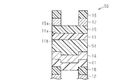
- the fragmentary sectional view which shows the partial cross section structure of the liquid crystal laminated body in one embodiment which actualized the liquid crystal laminated body of this invention.
- the partial expanded sectional view which expands and shows a part in sectional structure of a liquid crystal laminated body.
- the top view which shows the planar structure facing the 1st base material surface of a base material.
- the schematic diagram which shows typically schematic structure in the manufacturing apparatus of a liquid crystal laminated body. Process drawing which shows the process of forming the 1st laminated body in the manufacturing method of a liquid crystal laminated body. Process drawing which shows the process of forming the 2nd laminated body in the manufacturing method of a liquid crystal laminated body.
- Process drawing which shows the process of bonding the 1st laminated body and the 2nd laminated body in the manufacturing method of a liquid crystal laminated body.
- Process drawing which shows the process of irradiating light to the precursor layer in the manufacturing method of a liquid crystal laminated body.
- Process drawing which shows the process of peeling the 2nd base material in the manufacturing method of a liquid crystal laminated body.
- action of a liquid crystal laminated body The action figure for demonstrating the effect
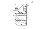
- Sectional drawing which shows the cross-section in the liquid crystal laminated body of a modification. Sectional drawing which shows the cross-section in the liquid crystal laminated body of a modification.
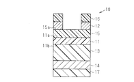
- the liquid crystal laminate 10 includes a base material 11, a metal layer 12, an adhesive layer 13, and a liquid crystal layer 14.
- the base material 11 includes a first base material surface 11a and a second base material surface 11b, and has light transmittance.
- the metal layer 12 faces a part of the first base material surface 11 a of the base material 11, and the adhesive layer 13 is a layer made of a photocurable resin and is positioned on the second base material surface 11 b of the base material 11. is doing.
- the liquid crystal layer 14 is located on the surface of the adhesive layer 13 opposite to the surface in contact with the substrate 11.
- the adhesive layer 13 that bonds the base material 11 and the liquid crystal layer 14 is formed of a photocurable resin. Therefore, compared with the structure in which the adhesive layer is formed of a thermosetting resin, the curing rate of the precursor layer for forming the adhesive layer 13 is high, and the time required for curing the precursor layer is short. Therefore, when an external force acts on the precursor layer before curing, the possibility that the precursor layer is deformed can be reduced, and as a result, deformation of the liquid crystal layer 14 accompanying deformation of the precursor layer can be suppressed.
- the liquid crystal laminate 10 further includes a diffraction layer 15.
- the diffraction layer 15 is located between the base material 11 and the metal layer 12 and is in contact with the base material 11 and the metal layer 12.
- the diffractive layer 15 has a diffractive structure on at least a part of the first diffractive surface 15 a that is the surface opposite to the surface in contact with the substrate 11. That is, the liquid crystal laminate 10 includes a base composed of a base material 11 and a diffractive layer 15, and the base is a first diffractive surface 15 a that is an example of a first surface and a second group that is an example of a second surface. It includes a material surface 11b and has optical transparency.
- the metal layer 12 is located on a part of the first base material surface 11a. According to the liquid crystal laminate 10, deformation of the liquid crystal layer 14 can be suppressed even in the configuration having the diffraction layer 15.
- the diffractive layer 15 at least a part of the first diffractive surface 15a is an uneven surface included in the diffractive structure.
- a portion overlapping the metal layer 12 is an uneven surface in a plan view of the substrate 11 facing the first substrate surface 11a.
- the metal layer 12 is preferably located on the uneven surface of the diffraction layer 15.
- the concave and convex surface and the metal layer 12 overlap, so that light incident on the diffractive layer 15 is easily reflected by the concave and convex surface and is emitted from the diffractive layer 15. The amount of light increases.
- the diffractive structure provided in the diffractive layer 15 may be any of a relief hologram, a volume hologram, and a diffraction grating, or a combination of two or more thereof.
- the liquid crystal laminate 10 further includes a mask layer 16, and the mask layer 16 is located on the surface of the metal layer 12 opposite to the surface in contact with the diffraction layer 15.
- the mask layer 16 is a mask used when the metal layer 12 is formed by etching, and has a shape that substantially overlaps the entire metal layer 12 in the thickness direction of the liquid crystal laminate 10.
- the liquid crystal laminate 10 includes the mask layer 16, the area of the metal layer 12 exposed to the outside is smaller than that of the configuration not including the mask layer 16. Therefore, it is possible to suppress the metal layer 12 from being chemically modified or physically damaged as compared with the configuration not including the mask layer 16.
- the liquid crystal laminate 10 further includes a protective layer 17, and the protective layer 17 is located on the surface of the liquid crystal layer 14 opposite to the surface in contact with the adhesive layer 13. Since the liquid crystal laminate 10 includes the protective layer 17, the area of the liquid crystal layer 14 that is exposed to the outside is smaller than in the configuration that does not include the protective layer 17. Therefore, the liquid crystal layer 14 can be prevented from being chemically modified or physically damaged as compared with a configuration in which the protective layer 17 is not provided.
- FIG. 2 shows an enlarged part of the cross-sectional structure of the liquid crystal laminate 10.
- the difference in crosslink density in the adhesive layer 13 is expressed by the difference in the density of dots applied to the adhesive layer 13.
- the adhesive layer 13 in the thickness direction of the adhesive layer 13, a portion that overlaps the metal layer 12 is a first portion 13a, and a portion that does not overlap the metal layer 12 is a second portion 13b. is there. That is, the adhesive layer 13 includes a first portion 13 a that overlaps the metal layer 12 in the thickness direction of the adhesive layer 13 and a second portion 13 b that does not overlap the metal layer 12 in the thickness direction of the adhesive layer 13. Yes.
- the crosslink density of the photocurable resin in the first portion 13a may be higher than the crosslink density of the photocurable resin in the second portion 13b.
- the difference in crosslink density between the first portion 13a and the second portion 13b is obtained by measuring the infrared spectrum of the first portion 13a and the infrared spectrum of the second portion 13b with a Fourier transform infrared spectroscopic device. This can be confirmed by comparing the measurement results.
- the crosslinking density in that part is low, while the unreacted substance capable of crosslinking in each part. If the absorption amount at the peak of the spectrum corresponding to the functional group is small, it can be said that the crosslink density at that portion is high. For this reason, the crosslinking density of a photocurable resin can be compared with the absorption amount in the peak of the spectrum corresponding to the unreacted functional group which can be bridge
- the adhesive layer 13 includes the first portion 13a and the second portion 13b having different crosslink densities, the hardness of the adhesive layer 13 is increased by the first portion 13a, and the second portion 13b is bonded.
- the adhesiveness between the layer 13 and the substrate 11 and the adhesiveness between the adhesive layer 13 and the liquid crystal layer 14 are enhanced.
- FIG. 3 shows the planar structure of the liquid crystal laminate 10 as viewed from the direction facing the mask layer 16. Note that FIG. 1 described above shows a cross-sectional structure taken along line II in FIG.
- the laminate of the mask layer 16 and the metal layer 12 is one of the surfaces of the diffraction layer 15 on the side opposite to the surface in contact with the substrate 11.
- the metal layer 12 includes a plurality of metal portions 12a
- the mask layer 16 also includes a plurality of mask portions 16a and the same number of mask portions 16a as the metal portions 12a. That is, the metal layer 12 has a pattern shape patterned into a predetermined shape, and the mask layer 16 also has almost the same pattern shape as the metal layer 12 in a plan view facing the mask layer 16.
- each metal portion 12a and each mask portion 16a have, for example, a star shape, but have other shapes such as a linear shape, a circular shape, and a polygonal shape. Also good. Or each metal part 12a and each mask part 16a may have a shape expressing a character and a symbol.
- the plurality of metal portions 12a and the plurality of mask portions 16a are not limited to the same shape but may have different shapes.
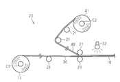
- the liquid crystal laminated body 10 is manufactured using the liquid crystal laminated body manufacturing apparatus 20, and the liquid crystal laminated body manufacturing apparatus 20 is a roll-to-roll apparatus.
- the liquid crystal laminate manufacturing apparatus 20 includes a plurality of rolls 21 and an irradiation unit 22.
- the liquid crystal laminate manufacturing apparatus 20 forms the first laminate 30 including the base material 11 while the base material 11, which is an example of the first base material wound around the first core C ⁇ b> 1, is conveyed by the roll 21. To do.
- the liquid crystal laminate manufacturing apparatus 20 forms the second laminate 40 including the second substrate 41 while the second substrate 41 taken up by the second core C2 is conveyed by the roll 21.
- the liquid-crystal laminated body manufacturing apparatus 20 bonds the 1st laminated body 30 and the 2nd laminated body 40, and with respect to the laminated body by which the 1st laminated body 30 and the 2nd laminated body 40 were bonded together, it is an irradiation part. By irradiating light from 22, the liquid crystal laminate 10 is manufactured.
- the method for manufacturing the liquid crystal laminate 10 includes a first base material surface 11a and a second base material surface 11b, and a metal layer facing a part of the first base material surface 11a in the base material 11 having optical transparency. 12 and positioning a precursor layer containing a photocurable resin in contact with the base material 11 and the liquid crystal layer 14 between the base material 11 and the liquid crystal layer 14. And the manufacturing method of the liquid crystal laminated body 10 is equipped with forming the contact bonding layer 13 by irradiating light to a precursor layer and hardening a precursor layer.
- the manufacturing method of the liquid crystal laminate 10 includes a first diffractive surface 15a and a second base material surface 11b, and a substrate having optical transparency is prepared, and a part of the substrate on the first diffractive surface 15a is prepared. Forming a metal layer 12. And the manufacturing method of the liquid-crystal laminated body 10 prepares the liquid-crystal layer 14, and makes the base
- the substrate The diffraction layer 15 is formed on the first first substrate surface 11a.
- the diffraction layer 15 is, for example, a step of applying a coating liquid containing various resins that are forming materials of the diffraction layer 15 to the first base material surface 11a of the base material 11 to form a coating film, It is formed through a step of curing the coating film while pressing a stamper for forming a diffractive structure on the surface opposite to the surface in contact with the substrate 11.
- a metal film for forming the metal layer 12 is formed on the entire first diffraction surface 15 a of the diffraction layer 15, and the mask layer 16 is formed on the surface of the metal film opposite to the diffraction layer 15.
- a resist material layer for forming is formed.
- the mask layer 16 is formed by patterning the resist material layer, and the metal layer 12 is etched using the mask layer 16, whereby the metal layer 12 facing a part of the first base material surface 11 a of the base material 11. Form.
- the precursor layer 31 for forming the above-described adhesive layer 13 is formed on the second substrate surface 11 b of the substrate 11.
- the precursor layer 31 is formed by applying a coating liquid containing a photocurable resin and a liquid organic compound for dispersing or dissolving the photocurable resin to the second substrate surface 11b of the substrate 11. It is formed. Thereby, the 1st laminated body 30 is obtained.
- the second stacked body 40 for forming the liquid crystal stacked body 10 is formed.
- the liquid crystal layer 14 is formed on one surface of the second base material 41.
- the liquid crystal layer 14 is formed, for example, through a step of applying a coating liquid containing a liquid crystal material to the second base material 41 to form a coating film, a step of drying the coating film, and a step of curing the liquid crystal material.
- the liquid crystal material forming the liquid crystal layer 14 includes, for example, a photocurable liquid crystal monomer having acrylates at both ends of the mesogenic group, a polymer liquid crystal that is cured by an electron beam or ultraviolet light, and a mesogenic group provided in the polymer main chain.
- a molecular liquid crystal and a liquid crystalline polymer in which the molecular main chain itself is aligned can be used.
- the orientation of these liquid crystals can be promoted by applying a coating liquid to form a coating film and then heat-treating the coating film at a temperature slightly below the NI point at which phase transition occurs.
- the first stacked body 30 and the second stacked body 40 are placed in a state where the precursor layer 31 included in the first stacked body 30 and the liquid crystal layer 14 included in the second stacked body 40 are opposed to each other. to paste together. Thereby, the precursor layer 31 containing the photocurable resin in contact with the base material 11 and the liquid crystal layer 14 is positioned between the base material 11 and the liquid crystal layer 14.
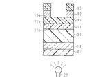
- the adhesive layer 13 is formed by irradiating the precursor layer 31 with light and thereby curing the precursor layer 31.
- the irradiation unit 22 is positioned on the opposite side of the precursor layer 31 from the metal layer 12, so that the precursor layer 31 is irradiated with light from the opposite side of the metal layer 12 toward the precursor layer 31.
- the precursor layer 31 is irradiated with light over a period of several seconds to several minutes.
- the adhesive layer 13 has a relatively high crosslink density to increase the hardness of the adhesive layer 13, and the relatively low crosslink density to the adhesive layer 13 and the substrate 11. The adhesion between the adhesive layer 13 and the liquid crystal layer 14 can be improved.
- the irradiation part 22 should just be selected from the lamp
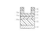
- the liquid crystal layer 14 is transferred to the base material 11 by peeling the second base material 41 from the liquid crystal layer 14. Then, a protective layer 17 is formed on the surface of the liquid crystal layer 14 opposite to the surface in contact with the adhesive layer 13.
- the protective layer 17 is formed through, for example, a step of applying a coating liquid for forming the protective layer 17 to the liquid crystal layer 14 to form a coating film, and a step of curing the coating film. Thereby, the liquid crystal laminate 10 having the configuration described above with reference to FIG. 1 is obtained.
- the operation of the liquid crystal laminate 10 will be described with reference to FIGS. 10 and 11.
- the liquid crystal laminate 10 described above has a photocurable resin adhesive layer 13 as an adhesive layer for adhering the liquid crystal layer 14 to the first laminate 30. Therefore, the cured adhesive layer 13 can be formed by irradiating the precursor layer 31 before curing with light for several seconds to several minutes.
- the laminate of the first laminate 30 and the second laminate 40 may be wound around the core immediately after the light irradiation of the precursor layer 31. At this time, the laminated body of the first laminated body 30 and the second laminated body 40 is wound around the core in a state where a pressure of, for example, several MPa is applied.
- the liquid crystal laminate has an adhesive layer made of a thermosetting resin as an adhesive layer for adhering the liquid crystal layer 14 to the first laminate 30, in order to cure the precursor layer, It is necessary to continue heating the precursor layer for several days. Therefore, the laminated body of the 1st laminated body 30 and the 2nd laminated body 40 is heated in the state wound around the winding core.
- the laminated body of the first laminated body 30 and the second laminated body 40 is heated in a state where a part of the second base material 41 is in contact with the mask layer 16. Therefore, the pressure by the mask layer 16 and the metal layer 12 is applied only to the portion of the precursor layer before curing that overlaps the portion of the second base material 41 in contact with the mask layer 16 in the thickness direction of the laminate. It is done.
- the precursor layer before curing has a hardness that is low enough to be deformed by the pressure applied from the mask layer 16 and the metal layer 12, while the substrate 11, the diffraction layer 15, the metal layer 12, and the mask layer 16 are Has higher hardness than the precursor layer. Therefore, until the precursor layer is cured, the mask layer 16 and the metal layer 12 are pressed against the portion of the precursor layer pressed against the base material 11 by the mask layer 16 and the metal layer 12. Marks appear.
- the adhesive layer 51 is deformed, and the liquid crystal layer 14 and the second base material 41 overlapping the adhesive layer 51 are also It deforms following the adhesive layer 51.
- the base material 11 only needs to have heat resistance and mechanical strength so that the base material 11 is not deformed by being softened when a heat pressure is applied to the base material 11 when the diffraction layer 15 is formed.
- the base material 11 may be an unstretched film manufactured by extrusion or casting, or a stretched film manufactured by stretching. Moreover, the base material 11 may be a uniaxially stretched film or a biaxially stretched film among the stretched films.
- the base material 11 may be, for example, cellophane, and the forming material of the base material 11 is polycarbonate (PC), polyethylene (PE), polypropylene (PP), polyolefin (PO), ethylene vinyl alcohol (EVOH), polyvinyl. Alcohol (PVA), polyvinyl chloride (PVC), polyethylene naphthalate (PEN), polyethylene terephthalate (PET), nylon, acrylic resin, triacetyl cellulose (TAC), polymethyl methacrylate, and polystyrene Good.
- PC polycarbonate
- PE polyethylene
- PP polypropylene
- PO polyolefin
- EVOH ethylene vinyl alcohol
- PVA polyvinyl chloride
- PEN polyethylene naphthalate
- PET polyethylene terephthalate
- nylon acrylic resin
- acrylic resin triacetyl cellulose
- TAC triacetyl cellulose
- TAC triacetyl cellulose
- the material for forming the base material 11 is not limited to the above-described synthetic resin, and may be natural resin, paper, synthetic paper, or the like as long as it has optical transparency.
- the substrate 11 may have a single-layer structure composed of only one layer formed from any of natural resin, paper, and synthetic paper, or may be composed of two or more layers. It may have a laminated structure.
- the thickness of the substrate 11 is preferably 12 ⁇ m or more and 100 ⁇ m or less from the viewpoint of improving each of the operability and workability of the substrate 11.
- the material for forming the diffraction layer 15 may be any material that can be molded using a stamper, and may be any of a thermoplastic resin, a thermosetting resin, an ultraviolet curable resin, and an electron beam curable resin.
- the thermoplastic resin include an acrylic resin, a cellulose resin, and a vinyl resin.
- the thermosetting resin is a urethane resin, a melamine resin, a phenol resin, or the like obtained by adding or crosslinking a polyisocyanate as a crosslinking agent to an acrylic polyol or polyester polyol having a reactive hydroxyl group.
- the ultraviolet curable resin and the electron beam curable resin include epoxy (meth) acryl and urethane (meth) acryl.
- the material for forming the diffraction layer 15 may be any one of the above-described materials, or a combination of two or more.
- the material for forming the diffractive layer 15 is not limited to the above-described material, but may be a diffractive structure such as a relief hologram, a volume hologram, or a diffraction grating, and has a concavo-convex structure for forming a diffraction image. Any material can be used.
- Metal layer As a material for forming the metal layer 12, a metal having high efficiency for reflecting light can be used. As a material for forming the metal layer 12, for example, aluminum (Al), tin (Sn), chromium (Cr), nickel (Ni), copper (Cu), gold (Au), or the like can be used.
- the metal layer 12 may have a single layer structure or may have a laminated structure composed of a plurality of layers having different forming materials.
- aluminum is preferable because it is less expensive than other metals and does not require the use of a strong acid or mixed acid as an etchant.
- a strong acid or mixed acid as an etchant.
- sodium hydroxide having a reduced concentration by dilution can be used.
- the above-described metal film for forming the metal layer 12 may be formed using, for example, a vacuum deposition method, a sputtering method, or the like.
- the thickness of the metal film that is, the thickness of the metal layer 12 increases the resistance of the metal layer 12 to moisture entering the metal layer 12 from the outside air, corrosive substances diffusing from the diffraction layer 15 to the metal layer 12, and the like. Above, it is preferable that it is 50 to 10,000 tons, and it is more preferable that it is 100 to 1000 tons.
- the material for forming the mask layer 16 may be any material having resistance to the etchant of the metal film and adhesion to the metal film.
- the material for forming the metal film is, for example, aluminum
- the material for forming the mask layer 16 is, for example, vinyl chloride-vinyl acetate copolymer, urethane resin, polyolefin resin, polyethyleneimine resin, acrylic resin, or silicone resin.
- the mask layer 16 may have a single layer structure, or may have a laminated structure composed of a plurality of layers having different formation materials.
- the material for forming the adhesive layer 13 may be a photocurable resin, and may be an ultraviolet curable resin or a visible light curable resin.
- the forming material of the adhesive layer 13 may include a first photocurable resin and a second photocurable resin.
- the first photocurable resin has a first crosslink density
- the second photocurable resin has a second crosslink density lower than the first crosslink density.
- the adhesive layer 13 is formed of the first photocurable resin.
- the hardness of the adhesive layer 13 is increased by the portion to be applied.
- the adhesiveness between the adhesive layer 13 and the substrate 11, and the adhesive layer 13 and the liquid crystal layer 14 Adhesiveness between is increased.
- the first photocurable resin portion of the adhesive layer 13 is the first portion. Yes, the second photo-curing resin portion is the second portion.
- the adhesive layer 13 preferably includes a plurality of first portions and a plurality of second portions, and the plurality of first portions and the plurality of second portions are preferably dispersed in the adhesive layer 13.
- the above-described photocurable resin is used in a state of being dispersed or dissolved in a liquid organic compound when the precursor layer 31 is formed.
- the liquid organic compound is preferably any one selected from the group consisting of toluene, methyl isobutyl ketone, and isopropyl alcohol.
- the pitch of the molecules constituting the cholesteric liquid crystal that is, the molecules of the liquid crystal material
- the color of light reflected by the liquid crystal layer 14 is changed.
- the precursor layer 31 is located between the substrate 11 and the liquid crystal layer 14, depending on the type of organic compound contained in the precursor layer 31, the organic compound diffuses into the liquid crystal layer 14, and molecular molecules in the liquid crystal layer 14 are There is a case to change the pitch.
- the liquid crystal layer 14 may reflect light having a color different from light having a desired color.
- the organic compound that disperses or dissolves the photocurable resin is any one of toluene, methyl isobutyl ketone, and isopropyl alcohol, the change of the molecular pitch in the liquid crystal layer 14 is suppressed, and the liquid crystal layer 14 is prevented from changing the color of the light reflected.
- the precursor layer 31 is irradiated with light through the second base material 41. Therefore, it is necessary to select a resin that is cured by light having a wavelength different from the light having the wavelength absorbed by the second base material 41 as the photocurable resin that forms the precursor layer 31. . Further, the irradiation unit 22 emits light having a wavelength other than the light having a wavelength absorbed by the second base material 41 and having a wavelength for curing the photocurable resin. It is necessary to use the configured irradiation unit 22.
- the forming material of the second base material 41 is PET and PET that transmits ultraviolet rays
- an ultraviolet curable resin can be used as the photocurable resin.
- a visible light curable resin can be used as the photocurable resin.
- the irradiation unit 22 may be a high-pressure mercury lamp.
- the PEN absorbs light having a wavelength of 365 nm, so that the photocurable resin is cured by light having a wavelength larger than 356 nm.
- the irradiation part 22 should just be comprised so that the light which has a wavelength larger than 365 nm may be radiated
- the hardness of the adhesive layer 13 is preferably as high as possible to suppress deformation of the adhesive layer 13. Therefore, even if the adhesive layer 13 has a high hardness, it is preferable that the adhesive layer 13 has an adhesive property that is high enough to develop an adhesive property between the substrate 11 and the liquid crystal layer 14. Therefore, the glass transition temperature is preferably 50 ° C. or higher, and more preferably 80 ° C. or higher.
- the second base material 41 is preferably a base material having flexibility and light transmission, in other words, a transparent base material.
- a stretched film manufactured using a stretching process can be used.
- the second substrate 41 may be a uniaxially stretched film or a biaxially stretched film among the stretched films.
- the stretched film may be, for example, cellophane, and the stretched film may be formed of, for example, PC, PE, PP, PO, EVOH, PVA, PVC, PEN, PET, nylon, acrylic resin, and TAC. I just need it. From the viewpoint of the strength of the stretched film, the ease of handling of the stretched film, and the light transmittance used to cure the adhesive layer 13, the stretch film forming material is preferably PET.
- the material for forming the liquid crystal layer 14 may be a liquid crystalline compound exhibiting a cholesteric liquid crystal state, or a liquid crystalline compound exhibiting a cholesteric phase, or a liquid crystalline compound in which a chiral compound is added to a compound exhibiting a nematic liquid crystal. Further, it may be a liquid crystalline compound exhibiting a chiral nematic phase.
- liquid crystalline compound for example, compounds represented by the following structural formulas 1 to 5 can be used.
- m and n are each an integer included in the range of 5 to 12, and in Structural Formula 2, m and n are any of the integers included in the range of 3 to 10, respectively.
- m is any integer included in the range of 6 to 20.
- l, m, and n are each an integer included in the range of 3 to 10
- Structural Formula 5 m and n are each an integer included in the range of 5 to 12, respectively. One of them.
- Ch in each of the structural formulas 1 to 5 is a structure represented by the following structural formula 6.
- one of the compounds represented by Structural Formulas 1 to 5 may be used, or two or more compounds may be used.
- the period in which the cholesteric liquid crystal can be displayed when the liquid crystal layer 14 is heated depends on the compound to be mixed and the proportion of each compound in the mixture. change. Therefore, when a mixture is used as the material for forming the liquid crystal layer 14, the type of compound to be mixed and the proportion of each compound in the mixture are set so that the period in which the cholesteric liquid crystal can be displayed is a desired period. There is a need to.
- the compounds represented by Structural Formulas 1 to 5 may be used as a material for forming the liquid crystal layer 14 in a state of being dispersed in a transparent resin binder.
- the resin binder may be, for example, polycarbonate, PMMA, polyvinyl alcohol, and polyamide.
- the protective layer 17 is a layer that has optical transparency and protects the liquid crystal layer 14 from ultraviolet rays and abrasion.
- various resins can be used depending on the function to be expressed in the protective layer 17.
- the protective layer 17 may have a single layer structure or may have a laminated structure composed of a plurality of layers having different formation materials.
- the protective layer 17 is a layer including a surface opposite to the surface in contact with the liquid crystal layer 14 and receives ink, pigment, and the like. You may have a layer that can.
- Example 1 A biaxially stretched PET film is prepared as the second substrate, and the cholesteric liquid crystal composition is applied to one surface of the second substrate using a wire bar so that the thickness after drying becomes 2 ⁇ m. A liquid crystal layer was formed by drying the liquid crystal composition.
- a cholesteric liquid crystal composition composed of a compound represented by the structural formula 1 and a methyl ketone solution and having a solid content of 30% by mass was used. This obtained the 2nd laminated body.
- the precursor layer in the first laminated body and the liquid crystal layer in the second laminated body were opposed to each other, and the first laminated body and the second laminated body were laminated by setting the linear pressure in the laminator to 50 N / cm.
- the ultraviolet-ray was irradiated with respect to the laminated body comprised from the 1st laminated body and the 2nd laminated body from the opposite side to the base material with respect to a precursor layer.
- the power of the ultraviolet ray was set to 500 mJ / cm 2 and the precursor layer was exposed for about 1 minute. Thereby, the adhesive layer was formed.
- the second substrate was peeled from the liquid crystal layer, and the liquid crystal layer was transferred to the substrate.
- the liquid crystal laminated body of Example 1 which has tolerance with respect to an ultraviolet-ray was obtained by coating a protective layer on the surface on the opposite side to the surface which contact
- a biaxially stretched PET film is prepared as the second substrate, and the cholesteric liquid crystal composition is applied to one surface of the second substrate using a wire bar so that the thickness after drying becomes 2 ⁇ m.
- a liquid crystal layer was formed by drying the liquid crystal composition.
- a cholesteric liquid crystal composition composed of a compound represented by the structural formula 1 and a methyl ketone solution and having a solid content of 30% by mass was used. This obtained the 2nd laminated body.
- the adhesive is composed of a thermosetting adhesive (Coronate L, manufactured by Tosoh Corporation) (Coronate is a registered trademark) and HDI (hexamethylene diisocyanate), and NCO / OH in the thermosetting adhesive and HDI.
- An adhesive having a ratio of 1.5 was used.
- the coated adhesive was heated at 100 ° C. for 30 seconds. Thereby, by drying the adhesive, a precursor layer was formed, and a first laminate was obtained.
- the precursor layer in the first laminate and the liquid crystal layer in the second laminate were opposed to each other, and the first laminate and the second laminate were laminated with the linear pressure in the laminator set to 50 N / cm. And the laminated body comprised from the 1st laminated body and the 2nd laminated body was aged at 60 degreeC over 3 days.
- the second substrate was peeled from the liquid crystal layer, and the liquid crystal layer was transferred to the substrate.
- the liquid crystal laminated body of the comparative example 1 which has tolerance with respect to an ultraviolet-ray was obtained by coating a protective layer on the surface on the opposite side to the surface which contact
- the laminated body of each test example 2 it was recognized that a mark on which the mask layer was pressed was formed in a portion of the base material in contact with the mask layer in the other laminated body. Moreover, in the laminated body of the laminated body of Test Example 2 including a base material having a mark against which the mask layer is pressed, the liquid crystal layer and the adhesive layer overlap with the traces of the base material in the thickness direction of the laminated body. It was recognized that a mark formed by pressing the mask layer was also formed on the part. Thus, according to the laminated body of Test Example 1, it was confirmed that the deformation of the liquid crystal layer accompanying the deformation of the adhesive layer can be suppressed.
- the effects listed below can be obtained.
- the adhesive layer 13 that bonds the base material 11 and the liquid crystal layer 14 is formed of a photocurable resin
- the adhesive layer 13 is compared with a configuration in which the adhesive layer 13 is formed of a thermosetting resin.
- the curing speed of the precursor layer 31 for forming is high, and the time required for curing the precursor layer 31 is short. Therefore, the possibility that the precursor layer 31 is deformed by an external force acting on the precursor layer 31 before curing can be reduced, and as a result, the deformation of the liquid crystal layer 14 accompanying the deformation of the precursor layer 31 can be suppressed.
- the adhesive layer 13 is configured by the first photocurable resin and the second photocurable resin, the portion of the adhesive layer 13 formed by the first photocurable resin. This increases the hardness of the adhesive layer.
- the adhesiveness between the adhesive layer 13 and the substrate 11, and between the adhesive layer 13 and the liquid crystal layer 14. Increases adhesion.
- the adhesive layer 13 has a first part 13a and a second part 13b having different crosslink densities
- the first part 13a increases the hardness of the adhesive layer 13, and the second part 13b
- the adhesiveness between the adhesive layer 13 and the substrate 11 and the adhesiveness between the adhesive layer 13 and the liquid crystal layer 14 are enhanced.
- the organic compound is any one of toluene, methyl isobutyl ketone, and isopropyl alcohol, it is possible to suppress a change in the molecular arrangement pitch in the liquid crystal layer 14, and the color of the light reflected from the liquid crystal layer 14 Change is suppressed.
- the amount of light applied to the portion overlapping the metal layer 12 in a plan view facing the first base material surface 11 a is greater than the amount of light applied to the other portions. It can be enlarged. Thereby, the crosslink density in the part which overlaps with the metal layer 12 among the contact bonding layers 13 can be raised rather than the other part in the contact bonding layer 13.
- the embodiment described above can be implemented with appropriate modifications as follows.
- the precursor layer 31 is exposed to the precursor from the side opposite to the liquid crystal layer 14.
- Light may be irradiated toward the layer 31.
- you may irradiate light toward the precursor layer 31 from the direction facing the precursor layer 31 among the directions crossing the thickness direction of the precursor layer 31. Even if it is such a structure, as long as the precursor layer 31 containing photocurable resin is hardened and the contact bonding layer 13 is formed, the effect equivalent to (1) mentioned above can be acquired.
- the precursor layer of the adhesive layer 13 may be formed on the surface of the liquid crystal layer 14 opposite to the surface in contact with the second base material 41. Even in such a configuration, the liquid crystal layer 14 and the base material 11 can be obtained by bringing the precursor layer located on the second base material 41 into contact with the second base material surface 11b of the base material 11 provided in the first laminate 30. It is possible to place a precursor layer between them.
- the organic compound that disperses or dissolves the photocurable resin may be an organic compound other than toluene, methyl isobutyl ketone, and isopropyl alcohol.
- Various organic compounds can be used as long as the liquid crystal layer 14 in contact with the adhesive layer 13 does not impair the function of reflecting light having a predetermined wavelength by the organic compound diffused from the adhesive layer 13.
- the material for forming the liquid crystal layer 14 is not limited to a compound showing a cholesteric phase, but may be a compound showing another liquid crystal, for example, a compound showing a nematic phase or a smectic phase.
- the crosslink density of the photocurable resin may be substantially uniform throughout the adhesive layer 13.
- the entire precursor layer 31 is irradiated with light that saturates the crosslinking density of the photocurable resin constituting the precursor layer 31. It is possible to make the crosslinking density of the photocurable resin substantially uniform.
- the diffraction layer 15 may be omitted.
- the metal layer 12 facing the part of the first substrate surface 11 a of the substrate 11 and the liquid crystal layer 14 are provided.
- the adhesive layer 13 made of photocurable resin is a liquid crystal laminate that is positioned between the base material 11 and the liquid crystal layer 14, the same effect as the above-described (1) can be obtained.
- the base body is composed of the base material 11, the first base material surface 11a is an example of the first surface, and the second base material surface 11b is an example of the second surface.
- the mask layer 16 may be omitted, and the mask layer 16 may be removed from the metal layer 12 after etching of the metal film for forming the metal layer 12 is performed. Even in such a configuration, similarly to the configuration in which the diffraction layer 15 is omitted, the metal layer 12 facing the part of the first substrate surface 11a of the substrate 11 and the liquid crystal layer 14 are included, and are photocurable. If the resin adhesive layer 13 is a liquid crystal laminate positioned between the base material 11 and the liquid crystal layer 14, the same effect as the above-described (1) can be obtained.
- the protective layer 17 may be omitted.
- the step of forming the protective layer 17 on the opposite surface may be omitted.
- the metal layer 12 facing the part of the first substrate surface 11a of the substrate 11 and the liquid crystal layer 14 are included, and are photocurable. If the resin adhesive layer 13 is a liquid crystal laminate positioned between the base material 11 and the liquid crystal layer 14, the same effect as the above-described (1) can be obtained.
- the liquid crystal laminate 60 may further include a background layer 61.
- the background layer 61 is a layer for enhancing the visibility of the liquid crystal layer 14 when the liquid crystal laminate 60 is viewed from the direction facing the protective layer 17.
- the background layer 61 may be a colored layer that is light transmissive and has a color different from the color of light reflected by the liquid crystal layer 14. It may be a light shielding layer that suppresses transmission of light toward the liquid crystal layer 14 from the opposite side.
- the background layer 61 is located in a portion of the diffraction layer 15 that is not covered with the metal layer 12 in the surface opposite to the surface in contact with the substrate 11, and the metal layer of the mask layer 16. 12 is located on the surface opposite to the surface in contact with 12.
- FIG. 13 shows, while the background layer 62 is located in the part which is not covered with the metal layer 12 in the surface on the opposite side to the surface which contacts the base material 11 among the diffraction layers 15.
- FIG. The mask layer 16 may not be located on the surface opposite to the surface in contact with the metal layer 12.
- the liquid crystal laminate 10 may have an adhesive layer, and the adhesive layer is a portion of the diffraction layer 15 that is not covered with the metal layer 12 in the surface opposite to the surface in contact with the substrate 11. And the mask layer 16 may be positioned on the surface opposite to the surface in contact with the metal layer 12.
- the liquid crystal laminate 60 described above with reference to FIG. 12 may have an adhesive layer.
- the adhesive layer is in contact with the diffraction layer 15 and the mask layer 16 in the background layer 61. It suffices if it is located on the surface opposite to the step surface.
- the liquid crystal laminate 60 described above with reference to FIG. 13 may have an adhesive layer.
- the adhesive layer is the surface of the background layer 62 that contacts the diffraction layer 15. It suffices that the opposite surface and the mask layer 16 are located on the surface opposite to the surface in contact with the metal layer 12.
- the liquid crystal laminate is wound around the core and is equivalent to the above (1). You can get an effect. Further, if the liquid crystal laminate does not have the background layers 61 and 62, the same effect as the above (1) is obtained in a state where the liquid crystal laminate is wound around the core before the adhesive layer is formed. I can.
Landscapes
- Physics & Mathematics (AREA)
- General Physics & Mathematics (AREA)
- Optics & Photonics (AREA)
- Engineering & Computer Science (AREA)
- Chemical & Material Sciences (AREA)
- Crystallography & Structural Chemistry (AREA)
- Computer Security & Cryptography (AREA)
- Manufacturing & Machinery (AREA)
- Laminated Bodies (AREA)
- Credit Cards Or The Like (AREA)
- Polarising Elements (AREA)
- Diffracting Gratings Or Hologram Optical Elements (AREA)
Abstract
液晶積層体は、第1回折面と第2基材面とを含み、光透過性を有する基体と、第1回折面の一部に位置する金属層と、第2基材面に位置する光硬化性樹脂製の接着層と、接着層のうち、基体に接する面とは反対側の面に位置する液晶層とを備える。
Description
本発明は、表示体の製造に用いることが可能な液晶積層体、および、液晶積層体の製造方法に関する。
有価証券や認証媒体には、これらの偽造を防止する目的で偽造の難しい表示体が付されている。こうした表示体には、ホログラムなどの回折構造を有する層である回折層と、回折層における凹凸面の一部に位置する金属層とを備える表示体が提案されている(例えば、特許文献1参照)。
また例えば、コレステリック液晶の状態を示す化合物製の層であって、表示体を観察する角度、すなわち、観察者の視線の方向を含む平面と表示体の表面とが形成する角度によって、外観や色が変わる液晶層を有した表示体が提案されている。この表示体は、基材、液晶層、および、熱接着性の接着層を備える液晶積層体のうち、液晶層を含む液晶積層体の一部が、接着層を用いて他の基体に転写されることによって形成される(例えば、特許文献2参照)。
ところで、表示体が有する偽造を防止する効果を高める上では、上述した2つの表示体を組み合わせることも提案されている。
この場合には、回折層と液晶層とを備える表示体の形成に用いられる積層体の製造において、回折層を有した回折積層体の基材に対して、液晶積層体が備える接着層を用いて液晶層が転写され、接着層に対して熱が与えられることで接着層が硬化される。
回折積層体に対する液晶層の転写は、積層体の量産性を高めるために、ロールツーロール法を用いて行われる。一方で、接着層の硬化には、通常、接着層に対して数日間にわたって熱を与える必要があるため、回折層と液晶層とを備える積層体が、巻芯に巻き取られた状態で接着層に対して熱が与えられる。
硬化前の接着層は、巻芯の径方向に沿って巻芯に向かう圧力が加わることによって、金属層の形状に追従して変形する程度の硬さしか有しないため、接着層と金属層とに挟まれる液晶層も、接着層とともに変形してしまう。
なお、こうした事情は、回折層を有しない積層体であって、液晶層と、基材の一部に対向する金属層とが、接着層を挟んで対向する積層体においても共通している。
本発明は、液晶層の変形を抑えることができる液晶積層体、および、液晶積層体の製造方法を提供することを目的とする。
本発明は、液晶層の変形を抑えることができる液晶積層体、および、液晶積層体の製造方法を提供することを目的とする。
上記課題を解決するための液晶積層体は、第1面と第2面とを含み、光透過性を有する基体と、前記第1面の一部に位置する金属層と、前記第2面に位置する光硬化性樹脂製の接着層と、前記接着層のうち、前記基体に接する面とは反対側の面に位置する液晶層と、を備える。
上記課題を解決するための液晶積層体の製造方法は、第1面と第2面とを含み、光透過性を有する基体を準備することと、前記基体の前記第1面の一部上に金属層を形成することと、液晶層を準備することと、前記基体の前記第2面と前記液晶層との間に、光硬化性樹脂を含む前駆層を前記基体と前記液晶層とに接するように位置させることと、前記前駆層に光を照射して前記前駆層を硬化させることによって、接着層を形成することと、を備える。
上記構成によれば、基体と液晶層とを接着する接着層が光硬化性樹脂で形成されているため、接着層が熱硬化性樹脂で形成される構成と比べて、接着層を形成するための前駆層の硬化速度が高く、前駆層の硬化に必要な時間が短い。それゆえに、硬化前の前駆層に対して、外力が働くことで前駆層が変形する可能性を低くでき、結果として、前駆層の変形に伴う液晶層の変形を抑えることができる。
図1から図11を参照して、液晶積層体、および、液晶積層体の製造方法を具体化した1つの実施形態を説明する。以下では、液晶積層体の構成、液晶積層体の製造方法、液晶積層体の作用、液晶積層体の形成材料、および、実施例を順番に説明する。
[液晶積層体の構成]
図1から図3を参照して液晶積層体の構成を説明する。
図1が示すように、液晶積層体10は、基材11、金属層12、接着層13、および、液晶層14を備えている。基材11は、第1基材面11aと第2基材面11bとを含み、光透過性を有している。金属層12は、基材11の第1基材面11aの一部と対向し、接着層13は、光硬化性樹脂製の層であって、基材11の第2基材面11bに位置している。液晶層14は、接着層13のうち、基材11に接する面とは反対側の面に位置している。
図1から図3を参照して液晶積層体の構成を説明する。
図1が示すように、液晶積層体10は、基材11、金属層12、接着層13、および、液晶層14を備えている。基材11は、第1基材面11aと第2基材面11bとを含み、光透過性を有している。金属層12は、基材11の第1基材面11aの一部と対向し、接着層13は、光硬化性樹脂製の層であって、基材11の第2基材面11bに位置している。液晶層14は、接着層13のうち、基材11に接する面とは反対側の面に位置している。
液晶積層体10によれば、基材11と液晶層14とを接着する接着層13が光硬化性樹脂で形成されている。そのため、接着層が熱硬化性樹脂で形成される構成と比べて、接着層13を形成するための前駆層の硬化速度が高く、前駆層の硬化に必要な時間が短い。それゆえに、硬化前の前駆層に対して外力が働くことによって、前駆層が変形する可能性を低くでき、結果として、前駆層の変形に伴う液晶層14の変形を抑えることができる。
液晶積層体10は、回折層15をさらに備えている。回折層15は、基材11と金属層12との間に位置し、かつ、基材11と金属層12とに接している。回折層15は、基材11に接する面とは反対側の面である第1回折面15aの少なくとも一部に回折構造を有している。すなわち、液晶積層体10は、基材11と回折層15とから構成される基体を備え、基体は第1面の一例である第1回折面15aと、第2面の一例である第2基材面11bとを含み、光透過性を有している。金属層12は、第1基材面11aの一部に位置している。こうした液晶積層体10によれば、回折層15を有する構成においても、液晶層14の変形を抑えることができる。
回折層15のうち、第1回折面15aの少なくとも一部が、回折構造に含まれる凹凸面である。第1回折面15aのうち、一部のみが凹凸面であるときには、基材11の第1基材面11aと対向する平面視において、金属層12と重なる部分が凹凸面であることが好ましい。言い換えれば、金属層12は、回折層15が有する凹凸面に位置することが好ましい。
第1基材面11aと対向する平面視において、凹凸面と金属層12とが重なることにより、回折層15に入射した光が、凹凸面にて反射されやすくなり、回折層15から射出される光の光量が大きくなる。
回折層15が備える回折構造は、レリーフ型ホログラム、体積型ホログラム、および、回折格子のいずれかであってもよいし、これらのうち2つ以上の組み合わせであってもよい。
液晶積層体10は、マスク層16をさらに備え、マスク層16は、金属層12のうち、回折層15に接する面とは反対側の面に位置している。マスク層16は、エッチングによって金属層12を形成するときに用いられるマスクであって、液晶積層体10の厚さ方向において、金属層12のほぼ全体に重なる形状を有している。
液晶積層体10がマスク層16を備えるため、マスク層16を備えていない構成と比べて、金属層12のうち、外部に露出する部分の面積が小さくなる。そのため、マスク層16を備えていない構成と比べて、金属層12が化学的に変性したり、物理的に損傷したりすることが抑えられる。
液晶積層体10は、さらに保護層17を備え、保護層17は、液晶層14のうち、接着層13に接する面とは反対側の面に位置している。液晶積層体10が保護層17を備えるため、保護層17を備えていない構成と比べて、液晶層14のうち、外部に露出する部分の面積が小さくなる。そのため、保護層17を備えていない構成と比べて、液晶層14が化学的に変性したり、物理的に損傷したりすることが抑えられる。
図2では、液晶積層体10の断面構造における一部が拡大して示されている。なお、図2では、説明の便宜上から、接着層13における架橋密度の違いを接着層13に付されたドットの密度の違いによって表現している。
図2が示すように、接着層13のうち、接着層13の厚さ方向において、金属層12と重なる部分が第1部分13aであり、金属層12とは重ならない部分が第2部分13bである。すなわち、接着層13は、接着層13の厚さ方向において金属層12と重なる第1部分13aと、接着層13の厚さ方向において金属層12とは重ならない第2部分13bとを有している。接着層13の中で、第1部分13aにおける光硬化性樹脂の架橋密度が、第2部分13bにおける光硬化性樹脂の架橋密度よりも高くてもよい。
第1部分13aと第2部分13bとの間での架橋密度の差は、フーリエ変換赤外分光装置によって第1部分13aの赤外線スペクトルと、第2部分13bの赤外線スペクトルとを計測し、これらの計測結果を比較することによって確認することができる。
各部分において架橋することが可能な未反応の官能基に対応するスペクトルのピークにおける吸収量が大きければ、その部分における架橋密度は低く、一方で、各部分において架橋することが可能な未反応の官能基に対応するスペクトルのピークにおける吸収量が小さければ、その部分における架橋密度は高いといえる。このため、光硬化性樹脂の架橋密度は、架橋することが可能な未反応の官能基に対応するスペクトルのピークにおける吸収量によって比較することができる。
なお、フーリエ変換赤外分光装置には、(株)日立ハイテクサイエンス製のNicolet iS50 FT-IRを用いることができる。
接着層13を構成する光硬化性樹脂では、光硬化性樹脂の架橋密度が高いほど接着層13の硬度が高くなる一方で、光硬化性樹脂の架橋密度が低いほど接着層13と接着層13に接する他の層との間の接着性が高まる。
そのため、接着層13が、架橋密度が互いに異なる第1部分13aと第2部分13bとを有していれば、第1部分13aによって接着層13の硬度が高まり、かつ、第2部分13bによって接着層13と基材11との間の接着性、および、接着層13と液晶層14との間の接着性が高まる。
図3は、液晶積層体10の平面構造であって、マスク層16と対向する方向から見た平面構造を示している。なお、先に説明した図1は、図3のうち、I-I線に沿う断面構造を示している。
図3が示すように、マスク層16と対向する平面視において、マスク層16と金属層12との積層体は、回折層15のうち、基材11に接する面とは反対側の面の一部に位置している。金属層12は、複数の金属部分12aから構成され、マスク層16も、複数のマスク部分16aであって、金属部分12aと同数のマスク部分16aから構成されている。すなわち、金属層12は、所定の形状にパターニングされたパターン状を有し、マスク層16も、マスク層16と対向する平面視において、金属層12とほぼ同じパターン状を有している。
マスク層16と対向する平面視において、各金属部分12aおよび各マスク部分16aは、例えば星形状を有しているが、直線状、円状、および、多角形状などの他の形状を有してもよい。あるいは、各金属部分12aおよび各マスク部分16aは、文字や記号を表現する形状を有してもよい。複数の金属部分12a、および、複数のマスク部分16aは、互いに同じ形状に限らず、互いに異なる形状を有してもよい。
[液晶積層体の製造方法]
図4から図9を参照して、液晶積層体10の製造方法を説明する。
なお、図4が示すように、液晶積層体10は、液晶積層体製造装置20を用いて製造され、液晶積層体製造装置20は、ロールツーロール装置である。液晶積層体製造装置20は、複数のロール21と、照射部22とを備えている。液晶積層体製造装置20は、第1巻芯C1に巻き取られた第1基材の一例である基材11をロール21によって搬送する間に、基材11を含む第1積層体30を形成する。また、液晶積層体製造装置20は、第2巻芯C2によって巻き取られた第2基材41をロール21によって搬送する間に、第2基材41を含む第2積層体40を形成する。
図4から図9を参照して、液晶積層体10の製造方法を説明する。
なお、図4が示すように、液晶積層体10は、液晶積層体製造装置20を用いて製造され、液晶積層体製造装置20は、ロールツーロール装置である。液晶積層体製造装置20は、複数のロール21と、照射部22とを備えている。液晶積層体製造装置20は、第1巻芯C1に巻き取られた第1基材の一例である基材11をロール21によって搬送する間に、基材11を含む第1積層体30を形成する。また、液晶積層体製造装置20は、第2巻芯C2によって巻き取られた第2基材41をロール21によって搬送する間に、第2基材41を含む第2積層体40を形成する。
そして、液晶積層体製造装置20は、第1積層体30と第2積層体40とを貼り合わせ、第1積層体30と第2積層体40とが貼り合わされた積層体に対して、照射部22から光を照射することによって、液晶積層体10を製造する。
液晶積層体10の製造方法は、第1基材面11aと第2基材面11bとを有し、光透過性を有する基材11における第1基材面11aの一部と対向する金属層12を形成することと、基材11と液晶層14との間に、基材11と液晶層14とに接する光硬化性樹脂を含む前駆層を位置させることとを備える。そして、液晶積層体10の製造方法は、前駆層に光を照射して前駆層を硬化させることによって、接着層13を形成することを備える。
すなわち、液晶積層体10の製造方法は、第1回折面15aと第2基材面11bとを含み、光透過性を有する基体を準備することと、基体の第1回折面15a上の一部に金属層12を形成することとを備える。そして、液晶積層体10の製造方法は、液晶層14を準備することと、基体の第2基材面11bと液晶層14との間に、光硬化性樹脂を含む前駆層を基体と液晶層14とに接するように位置させることとを備える。さらに、液晶積層体10の製造方法は、前駆層に光を照射して前駆層を硬化させることによって、接着層13を形成することを備える。
すなわち、図5が示すように、液晶積層体10の製造方法では、液晶積層体10を形成するための第1積層体30を形成し、第1積層体30を形成するときには、まず、基材11の第1基材面11aに回折層15を形成する。回折層15は、例えば、基材11の第1基材面11aに回折層15の形成材料である各種樹脂を含む塗液を塗工して塗膜を形成する工程と、塗膜のうち、基材11に接する面とは反対側の面に回折構造を形成するためのスタンパを押し当てつつ、塗膜を硬化させる工程とを経て形成される。
次いで、回折層15のうち、第1回折面15aの全体に、金属層12を形成するための金属膜を形成し、金属膜のうち、回折層15とは反対側の面にマスク層16を形成するためのレジスト材料層を形成する。そして、レジスト材料層をパターニングすることによってマスク層16を形成し、マスク層16を用いて金属層をエッチングすることによって、基材11の第1基材面11aの一部と対向する金属層12を形成する。
そして、基材11の第2基材面11bに、上述した接着層13を形成するための前駆層31を形成する。前駆層31は、光硬化性樹脂と、光硬化性樹脂を分散または溶解させるための液体状の有機化合物とを含む塗液を、基材11の第2基材面11bに塗工することによって形成される。これにより、第1積層体30を得る。
一方で、図6が示すように、液晶積層体10を形成するための第2積層体40を形成する。第2積層体40を形成するときには、第2基材41が有する1つの面に、液晶層14を形成する。液晶層14は、例えば、液晶材料を含む塗液を第2基材41に塗工して塗膜を形成する工程と、塗膜を乾燥させる工程と、液晶材料を硬化させる工程を経て形成される。なお、液晶層14を形成する液晶材料には、例えば、メソゲン基の両端にアクリレートを備える光硬化型液晶モノマー、電子線もしくは紫外線で硬化する高分子液晶、ポリマー主鎖にメソゲン基を提げた高分子液晶、および、分子主鎖自体が配向する液晶性高分子を用いることができる。これらの液晶は、塗液を塗工して塗膜を形成した後、相転移を起こすNI点よりも少し下の温度で塗膜を熱処理することによって、配向を促進させることが可能である。
図7が示すように、第1積層体30が備える前駆層31と、第2積層体40が備える液晶層14とを対向させた状態で、第1積層体30と第2積層体40とを貼り合わせる。これにより、基材11と液晶層14との間に、基材11と液晶層14とに接する光硬化性樹脂を含む前駆層31を位置させる。
図8が示すように、前駆層31に対して光を照射し、これにより前駆層31を硬化させることで、接着層13を形成する。このとき、前駆層31に対して金属層12とは反対側に照射部22を位置させることで、前駆層31に対して金属層12とは反対側から前駆層31に向けて光を照射する。前駆層31に対して、例えば数秒以上数分以下の間にわたって光を照射する。
これにより、基材11の第1基材面11aと対向する平面視にて、接着層13のうち、金属層12と重なる部分において、金属層12にて反射された光が照射される分だけ、他の部分よりも照射される光の光量を大きくすることが可能になる。そのため、接着層13のうち、金属層12と重なる部分での架橋密度を、接着層13における他の部分よりも高めることが可能である。それゆえに、接着層13のうち、相対的に架橋密度が高い部分によって、接着層13の硬度を高め、相対的に架橋密度が低い部分によって、接着層13と基材11との接着性、および、接着層13と液晶層14との接着性を高めることができる。
なお、照射部22は、光硬化性樹脂を硬化させることが可能な光の波長に応じて、紫外線を照射するランプ、および、可視光線を照射するランプなどから選択されればよい。
図9が示すように、液晶層14から第2基材41を剥離することによって、液晶層14を基材11に転写する。そして、液晶層14のうち、接着層13に接する面とは反対側の面に、保護層17を形成する。保護層17は、例えば、保護層17を形成するための塗液を液晶層14に塗工して塗膜を形成する工程と、塗膜を硬化させる工程とを経て形成される。これにより、図1を参照して先に説明された構成を有する液晶積層体10を得る。
[液晶積層体の作用]
図10および図11を参照して、液晶積層体10の作用を説明する。
上述した液晶積層体10は、第1積層体30に対して液晶層14を接着させる接着層として光硬化性樹脂製の接着層13を有する。そのため、硬化前の前駆層31に対して数秒以上数分以下にわたって光を照射すれば、硬化した接着層13を形成することができる。
図10および図11を参照して、液晶積層体10の作用を説明する。
上述した液晶積層体10は、第1積層体30に対して液晶層14を接着させる接着層として光硬化性樹脂製の接着層13を有する。そのため、硬化前の前駆層31に対して数秒以上数分以下にわたって光を照射すれば、硬化した接着層13を形成することができる。
ここで、液晶積層体10の製造工程において、前駆層31に対する光の照射の直後に、第1積層体30と第2積層体40との積層体が巻芯に巻き取られる場合もある。このとき、第1積層体30と第2積層体40との積層体は、例えば数MPaの圧力が掛けられた状態で、巻芯に巻き付けられる。
これにより、図10が示すように、第2基材41の一部がマスク層16に接するため、第2基材41の一部のみに対して、マスク層16と金属層12との積層体が押し付けられる。上述したように、前駆層31は、前駆層31に対する光の照射が行われた時点でほぼ硬化が完了している。そのため、第2基材41の一部のみに対してマスク層16と金属層12との積層体が押し付けられたとしても、接着層13、ひいては液晶層14と第2基材41とに、マスク層16と金属層12とが押し付けられた痕が生じることが抑えられる。
これに対して、第1積層体30に対して液晶層14を接着させる接着層として、熱硬化性樹脂製の接着層を液晶積層体が有する構成では、前駆層を硬化させるためには、通常、数日間にわたって前駆層を加熱し続ける必要がある。そのため、第1積層体30と第2積層体40との積層体は、巻芯に巻き付けられた状態で加熱される。
これにより、第2基材41の一部がマスク層16に接する状態で、第1積層体30と第2積層体40との積層体が加熱される。そのため、硬化前の前駆層のうち、積層体の厚さ方向において、第2基材41の中でマスク層16に接する部分と重なる部分にのみ、マスク層16と金属層12とによる圧力が加えられる。
硬化前の前駆層は、マスク層16と金属層12とから加えられる圧力によって変形する程度に低い硬度を有する一方で、基材11、回折層15、金属層12、および、マスク層16は、前駆層よりも高い硬度を有する。それゆえに、前駆層が硬化するまでの間において、前駆層のうち、マスク層16と金属層12とによって基材11に向けて押し付けられた部分に、マスク層16と金属層12とによって押し付けられた痕が生じる。
結果として、図11が示すように、熱硬化性樹脂製の接着層51を有する液晶積層体50では、接着層51が変形し、接着層51に重なる液晶層14および第2基材41も、接着層51に追従して変形する。
[液晶積層体の形成材料]
液晶積層体10を形成するための各層の形成材料を説明する。
[基材]
基材11は、回折層15の形成時に基材11に熱圧が与えられたとき、軟化することによって変形しない程度の耐熱性と機械的な強度とを有していればよい。基材11は、押出加工やキャスト加工によって製造された無延伸フィルムであってもよいし、延伸加工によって製造された延伸フィルムであってもよい。また、基材11は、延伸フィルムのうち、1軸延伸フィルムであってもよいし、2軸延伸フィルムであってもよい。
液晶積層体10を形成するための各層の形成材料を説明する。
[基材]
基材11は、回折層15の形成時に基材11に熱圧が与えられたとき、軟化することによって変形しない程度の耐熱性と機械的な強度とを有していればよい。基材11は、押出加工やキャスト加工によって製造された無延伸フィルムであってもよいし、延伸加工によって製造された延伸フィルムであってもよい。また、基材11は、延伸フィルムのうち、1軸延伸フィルムであってもよいし、2軸延伸フィルムであってもよい。
基材11は、例えばセロハンであってもよいし、基材11の形成材料は、ポリカーボネート(PC)、ポリエチレン(PE)、ポリプロピレン(PP)、ポリオレフィン(PO)、エチレンビニルアルコール(EVOH)、ポリビニルアルコール(PVA)、ポリ塩化ビニル(PVC)、ポリエチレンナフタレート(PEN)、ポリエチレンテレフタレート(PET)、ナイロン、アクリル樹脂、トリアセチルセルロース(TAC)、ポリメタクリル酸メチル、および、ポリスチレンなどであってもよい。
なお、基材11の形成材料は、上述した合成樹脂に限らず、光透過性を有していれば、天然樹脂、紙、および、合成紙などであってもよい。また、基材11は、天然樹脂、紙、および、合成紙のいずれかから形成された1つの層のみから構成される単層構造を有してもよいし、2つ以上の層から構成される積層構造を有してもよい。
基材11の厚さは、基材11の操作性および加工性の各々を高める観点から、12μm以上100μm以下であることが好ましい。
[回折層]
回折層15の形成材料は、スタンパを用いた成形が可能な材料であればよく、熱可塑性樹脂、熱硬化性樹脂、紫外線硬化性樹脂、および、電子線硬化性樹脂のいずれであってもよい。熱可塑性樹脂は、例えば、アクリル系樹脂、セルロース系樹脂、および、ビニル系樹脂などである。熱硬化性樹脂は、反応性を有した水酸基を有するアクリルポリオールやポリエステルポリオールなどにポリイソシアネートを架橋剤として添加または架橋したウレタン樹脂、メラミン系樹脂、および、フェノール樹脂などである。紫外線硬化性樹脂および電子線硬化性樹脂は、エポキシ(メタ)アクリル、および、ウレタン(メタ)アクリルなどである。
回折層15の形成材料は、スタンパを用いた成形が可能な材料であればよく、熱可塑性樹脂、熱硬化性樹脂、紫外線硬化性樹脂、および、電子線硬化性樹脂のいずれであってもよい。熱可塑性樹脂は、例えば、アクリル系樹脂、セルロース系樹脂、および、ビニル系樹脂などである。熱硬化性樹脂は、反応性を有した水酸基を有するアクリルポリオールやポリエステルポリオールなどにポリイソシアネートを架橋剤として添加または架橋したウレタン樹脂、メラミン系樹脂、および、フェノール樹脂などである。紫外線硬化性樹脂および電子線硬化性樹脂は、エポキシ(メタ)アクリル、および、ウレタン(メタ)アクリルなどである。
なお、回折層15の形成材料は、上述した材料のいずれか1つであってもよいし、2つ以上の組み合わせであってもよい。また、回折層15の形成材料は、上述した材料に限らず、レリーフ型ホログラム、体積型ホログラム、および、回折格子などの回折構造であって、回折像を形成するための凹凸構造を有することが可能な材料であればよい。
[金属層]
金属層12の形成材料には、光を反射する効率の高い金属を用いることができる。金属層12の形成材料には、例えば、アルミニウム(Al)、スズ(Sn)、クロム(Cr)、ニッケル(Ni)、銅(Cu)、および、金(Au)などを用いることができる。金属層12は、単層構造を有してもよいし、形成材料が互いに異なる複数の層から構成される積層構造を有してもよい。
金属層12の形成材料には、光を反射する効率の高い金属を用いることができる。金属層12の形成材料には、例えば、アルミニウム(Al)、スズ(Sn)、クロム(Cr)、ニッケル(Ni)、銅(Cu)、および、金(Au)などを用いることができる。金属層12は、単層構造を有してもよいし、形成材料が互いに異なる複数の層から構成される積層構造を有してもよい。
上述した形成材料のうち、アルミニウムは、他の金属と比べて安価である点、および、エッチャントとして強酸や混酸を用いる必要のない点で好ましい。アルミニウムのエッチャントには、希釈によって濃度の低められた水酸化ナトリウムを用いることができる。
金属層12を形成するための上述した金属膜は、例えば、真空蒸着法、および、スパッタ法などを用いて形成すればよい。金属膜の厚さ、すなわち、金属層12の厚さは、外気から金属層12に進入する水分や、回折層15から金属層12に拡散する腐食性の物質などに対する金属層12の耐性を高める上で、50Å以上10000Å以下であることが好ましく、100Å以上1000Å以下であることがより好ましい。
[マスク層]
マスク層16の形成材料は、金属膜のエッチャントに対する耐性を有し、かつ、金属膜に対して密着性を有する材料であればよい。金属膜の形成材料が、例えばアルミニウムであるときには、マスク層16の形成材料には、例えば、塩化ビニル‐酢酸ビニル共重合体、ウレタン樹脂、ポリオレフィン樹脂、ポリエチレンイミン樹脂、アクリル樹脂、シリコーン樹脂などを用いることができる。なお、マスク層16は、単層構造を有してもよいし、各層の形成材料が互いに異なる複数の層から構成された積層構造を有してもよい。
マスク層16の形成材料は、金属膜のエッチャントに対する耐性を有し、かつ、金属膜に対して密着性を有する材料であればよい。金属膜の形成材料が、例えばアルミニウムであるときには、マスク層16の形成材料には、例えば、塩化ビニル‐酢酸ビニル共重合体、ウレタン樹脂、ポリオレフィン樹脂、ポリエチレンイミン樹脂、アクリル樹脂、シリコーン樹脂などを用いることができる。なお、マスク層16は、単層構造を有してもよいし、各層の形成材料が互いに異なる複数の層から構成された積層構造を有してもよい。
[接着層]
接着層13の形成材料は、光硬化性樹脂であればよく、紫外線硬化性樹脂であってもよいし、可視光硬化性樹脂であってもよい。
接着層13の形成材料は、光硬化性樹脂であればよく、紫外線硬化性樹脂であってもよいし、可視光硬化性樹脂であってもよい。
接着層13の形成材料は、第1の光硬化性樹脂と第2の光硬化性樹脂とを含んでもよい。この場合には、第1の光硬化性樹脂は、第1の架橋密度を有し、第2の光硬化性樹脂は、第1の架橋密度よりも低い第2の架橋密度を有することが好ましい。
接着層13の形成材料が、架橋密度の互いに異なる第1の光硬化性樹脂と第2の光硬化性樹脂とを含んでいれば、接着層13のうち、第1の光硬化性樹脂によって形成される部分によって接着層13の硬度が高まる。これに対して、接着層13のうち、第2の光硬化性樹脂によって形成される部分によって、接着層13と基材11との間の接着性、および、接着層13と液晶層14との間の接着性が高まる。
接着層13の形成材料が第1の光硬化性樹脂と第2の光硬化性樹脂とを含む場合には、接着層13のうち、第1の光硬化性樹脂製の部分が第1部分であり、第2の光硬化性樹脂製の部分が第2の部分である。接着層13は、複数の第1部分と、複数の第2部分とを有し、接着層13の中で、複数の第1部分と複数の第2部分とが分散していることが好ましい。
上述した光硬化性樹脂は、前駆層31を形成するとき、液体状の有機化合物に分散あるいは溶解した状態で用いられる。液体状の有機化合物は、トルエン、メチルイソブチルケトン、および、イソプロピルアルコールから構成される群から選択されるいずれか1つであることが好ましい。
ここで、コレステリック液晶において、コレステリック液晶を構成する化合物すなわち液晶材料の分子が並ぶピッチが変わると、液晶層14において反射される光の色が変わる。そして、前駆層31が基材11と液晶層14との間に位置すると、前駆層31に含まれる有機化合物の種類によっては、有機化合物が液晶層14に拡散して、液晶層14における分子の並ぶピッチを変える場合がある。これにより、液晶層14が、所望とする色を有した光とは異なる色を有した光を反射する場合もある。
この点で、光硬化性樹脂を分散あるいは溶解する有機化合物が、トルエン、メチルイソブチルケトン、および、イソプロピルアルコールのいずれかであれば、液晶層14における分子のピッチが変わることが抑えられ、液晶層14において反射される光の有する色が変わることが抑えられる。
一方で、前駆層31には、第2基材41を通して光が照射される。そのため、前駆層31を形成する光硬化性樹脂には、第2基材41によって吸収される波長を有した光とは異なる波長を有した光によって硬化する樹脂が選択されることが必要である。また、照射部22には、第2基材41によって吸収される波長の光以外の波長を有した光であって、かつ、光硬化性樹脂を硬化させる波長を有した光を放射するように構成された照射部22を用いることが必要である。
例えば、第2基材41の形成材料がPETであり、かつ、紫外線を透過するPETであれば、光硬化性樹脂には、紫外線硬化性樹脂を用いることができる。また、第2基材41の形成材料として、紫外線を吸収するPETを用いた場合には、光硬化性樹脂には、可視光硬化性樹脂を用いることができる。これらの場合には、照射部22が高圧水銀ランプであればよい。
また例えば、第2基材41の形成材料がPENである場合には、PENが365nmの波長を有した光を吸収するため、光硬化性樹脂が、356nmよりも大きい波長を有した光によって硬化する樹脂であり、照射部22が、365nmよりも大きい波長を有した光を放射するように構成されていればよい。
また、液晶積層体10が巻芯に巻き付けられたとき、接着層13の変形を抑える上では、接着層13の硬度は高いほど好ましい。そのため、接着層13には、接着層13の硬度が高くとも、基材11と液晶層14とに接着性を発現する程度に高い接着性を有することが好ましい。それゆえに、ガラス転移温度は、50℃以上であることが好ましく、80℃以上であることがより好ましい。
[第2基材]
第2基材41は、可撓性を有し、かつ、光透過性を有する、言い換えれば透明である基材であることが好ましい。第2基材41には、延伸加工を用いて製造された延伸フィルムを用いることができる。第2基材41は、延伸フィルムのうち、1軸延伸フィルムであってもよいし、2軸延伸フィルムであってもよい。
第2基材41は、可撓性を有し、かつ、光透過性を有する、言い換えれば透明である基材であることが好ましい。第2基材41には、延伸加工を用いて製造された延伸フィルムを用いることができる。第2基材41は、延伸フィルムのうち、1軸延伸フィルムであってもよいし、2軸延伸フィルムであってもよい。
延伸フィルムは、例えばセロハンであってもよいし、延伸フィルムの形成材料は、例えば、PC、PE、PP、PO、EVOH、PVA、PVC、PEN、PET、ナイロン、アクリル樹脂、および、TACなどであればよい。延伸フィルムの強度、延伸フィルムの取り扱いの容易さ、および、接着層13の硬化に用いられる光の透過性の点から、延伸フィルムの形成材料は、PETであることが好ましい。
[液晶層]
液晶層14の形成材料は、コレステリック液晶の状態を示す液晶性化合物であればよく、コレステリック相を示す液晶性化合物でもよいし、ネマチック液晶を示す化合物に対してキラル化合物が添加された液晶性化合物であって、キラルネマチック相を示す液晶性化合物であってもよい。
液晶層14の形成材料は、コレステリック液晶の状態を示す液晶性化合物であればよく、コレステリック相を示す液晶性化合物でもよいし、ネマチック液晶を示す化合物に対してキラル化合物が添加された液晶性化合物であって、キラルネマチック相を示す液晶性化合物であってもよい。
液晶性化合物には、例えば、以下の構造式1から構造式5に示される化合物を用いることができる。





なお、構造式1において、mおよびnは、それぞれ5から12の範囲に含まれる整数のいずれかであり、構造式2において、mおよびnは、それぞれ3から10の範囲に含まれる整数のいずれかであり、構造式3において、mは6から20の範囲に含まれる整数のいずれかである。構造式4において、l、m、および、nは、それぞれ3から10の範囲に含まれる整数のいずれかであり、構造式5において、mおよびnは、それぞれ5から12の範囲に含まれる整数のいずれかである。
また、構造式1から構造式5の各々におけるChは、以下の構造式6で示される構造である。
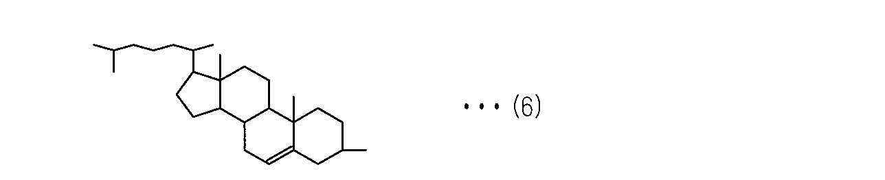
液晶層14の形成材料として、構造式1から構造式5で示される化合物のうちの1つを用いてもよいし、2つ以上を用いてもよい。2つ以上の化合物を混合して用いる場合には、混合する化合物、および、混合物において各化合物が占める割合に応じて、液晶層14が加熱されたときに、コレステリック液晶を示すことのできる期間が変わる。そのため、液晶層14の形成材料として混合物を用いる場合には、コレステリック液晶を示すことのできる期間が所望の期間となるように、混合する化合物の種類、および、混合物において各化合物が占める割合を設定する必要がある。
構造式1から構造式5で示される化合物は、透明な樹脂バインダに分散させた状態で、液晶層14の形成材料として用いてもよい。樹脂バインダは、例えば、ポリカーボネート、PMMA、ポリビニルアルコール、および、ポリアミドなどであればよい。
[保護層]
保護層17は、光透過性を有し、液晶層14を紫外線や摩耗などから保護する層である。保護層17の形成材料には、保護層17に発現させる機能に応じて、各種の樹脂を用いることができる。保護層17は、単層構造を有してもよいし、形成材料の互いに異なる複数の層から構成される積層構造を有してもよい。また、保護層17が単層構造および積層構造のいずれを有する場合であっても、保護層17は、液晶層14に接する面とは反対側の面を含む層として、インキおよび顔料などを受容することができる層を有してもよい。
保護層17は、光透過性を有し、液晶層14を紫外線や摩耗などから保護する層である。保護層17の形成材料には、保護層17に発現させる機能に応じて、各種の樹脂を用いることができる。保護層17は、単層構造を有してもよいし、形成材料の互いに異なる複数の層から構成される積層構造を有してもよい。また、保護層17が単層構造および積層構造のいずれを有する場合であっても、保護層17は、液晶層14に接する面とは反対側の面を含む層として、インキおよび顔料などを受容することができる層を有してもよい。
[実施例]
[実施例1]
第2基材として2軸延伸のPETフィルムを準備し、第2基材の1つの面にコレステリック液晶組成物を乾燥後の厚さが2μmとなるようにワイヤーバーを用いて塗工し、コレステリック液晶組成物を乾燥させることによって、液晶層を形成した。なお、コレステリック液晶組成物として、構造式1で示される化合物と、メチルケトン溶液とから構成され、組成物における固形分が30質量%であるコレステリック液晶組成物を用いた。これにより、第2積層体を得た。
[実施例1]
第2基材として2軸延伸のPETフィルムを準備し、第2基材の1つの面にコレステリック液晶組成物を乾燥後の厚さが2μmとなるようにワイヤーバーを用いて塗工し、コレステリック液晶組成物を乾燥させることによって、液晶層を形成した。なお、コレステリック液晶組成物として、構造式1で示される化合物と、メチルケトン溶液とから構成され、組成物における固形分が30質量%であるコレステリック液晶組成物を用いた。これにより、第2積層体を得た。
基材、回折層、金属層、および、マスク層から構成される積層体を準備し、基材のうち、回折層が位置する面とは反対側の面に、ワイヤーバーを用いて光硬化性接着剤(ユニディックV-9511、DIC(株)製)(ユニディックは登録商標)を塗工した。塗工した光硬化性接着剤を100℃にて30秒間にわたって加熱した。これにより、光硬化性接着剤を乾燥させることによって前駆層を形成し、第1積層体を得た。
次いで、第1積層体における前駆層と、第2積層体における液晶層とを対向させ、第1積層体と第2積層体とをラミネーターにおける線圧を50N/cmに設定してラミネートした。そして、第1積層体と第2積層体とから構成された積層体に対して、前駆層に対する基材とは反対側から紫外線を照射した。このとき、UV照射装置において、紫外線のパワーを500mJ/cm2に設定し、約1分間にわたって前駆層を露光した。これにより、接着層を形成した。
接着層を形成した後、第2基材を液晶層から剥離して、液晶層を基材に転写した。そして、液晶層のうち、接着層に接する面とは反対側の面に保護層を塗工することによって、紫外線に対して耐性を有する実施例1の液晶積層体を得た。
[比較例1]
第2基材として2軸延伸のPETフィルムを準備し、第2基材の1つの面にコレステリック液晶組成物を乾燥後の厚さが2μmとなるようにワイヤーバーを用いて塗工し、コレステリック液晶組成物を乾燥させることによって、液晶層を形成した。なお、コレステリック液晶組成物として、構造式1で示される化合物と、メチルケトン溶液とから構成され、組成物における固形分が30質量%であるコレステリック液晶組成物を用いた。これにより、第2積層体を得た。
第2基材として2軸延伸のPETフィルムを準備し、第2基材の1つの面にコレステリック液晶組成物を乾燥後の厚さが2μmとなるようにワイヤーバーを用いて塗工し、コレステリック液晶組成物を乾燥させることによって、液晶層を形成した。なお、コレステリック液晶組成物として、構造式1で示される化合物と、メチルケトン溶液とから構成され、組成物における固形分が30質量%であるコレステリック液晶組成物を用いた。これにより、第2積層体を得た。
基材、回折層、金属層、および、マスク層から構成される積層体を準備し、基材のうち、回折層が位置する面とは反対側の面に、接着剤を乾燥後の厚さが2μmとなるようにワイヤーバーを用いて塗工した。なお、接着剤として、熱硬化性接着剤(コロネートL、東ソー(株)製)(コロネートは登録商標)とHDI(ヘキサメチレンジイソシアネート)とから構成され、熱硬化性接着剤とHDIにおけるNCO/OH比が1.5である接着剤を用いた。塗工した接着剤を100℃にて30秒間にわたって加熱した。これにより、接着剤を乾燥させることによって、前駆層を形成し、第1積層体を得た。
次いで、第1積層体における前駆層と、第2積層体における液晶層とを対向させ、第1積層体と第2積層体とをラミネーターにおける線圧を50N/cmに設定してラミネートした。そして、第1積層体と第2積層体とから構成された積層体を60℃にて3日間にわたってエージングした。
エージングによって前駆層を硬化することで接着層を形成した後、第2基材を液晶層から剥離して、液晶層を基材に転写した。そして、液晶層のうち、接着層に接する面とは反対側の面に保護層を塗工することによって、紫外線に対して耐性を有する比較例1の液晶積層体を得た。
[評価方法および評価結果]
実施例1の液晶積層体の製造工程のうち、第1積層体と第2積層体とをラミネートする工程までが完了した複数の積層体を準備し、各積層体を試験例1の積層体とした。また、比較例1の液晶積層体の製造方法のうち、第1積層体と第2積層体とをラミネートする工程までが完了した複数の積層体を準備し、各積層体を試験例2の積層体とした。
実施例1の液晶積層体の製造工程のうち、第1積層体と第2積層体とをラミネートする工程までが完了した複数の積層体を準備し、各積層体を試験例1の積層体とした。また、比較例1の液晶積層体の製造方法のうち、第1積層体と第2積層体とをラミネートする工程までが完了した複数の積層体を準備し、各積層体を試験例2の積層体とした。
そして、複数の試験例1の積層体を重ねた状態で、複数の試験例1の積層体に対して5MPaの圧力を加えながら、約1分間にわたって複数の積層体に対して紫外線を照射し、複数の試験例1の積層体に対して1日間にわたって圧力を加え続けた。これに対して、複数の試験例2の積層体を重ねた状態で、複数の試験例2の積層体に対して5MPaの圧力を加えながら、60℃の雰囲気に1日間にわたって静置した。
各試験例1の積層体では、基材のうち、他の積層体におけるマスク層と接する部分、および、液晶層および接着層のうち、積層体の厚さ方向において他の積層体におけるマスク層と重なる部分が、ほぼ変形していないことが認められた。
一方で、各試験例2の積層体では、基材のうち、他の積層体におけるマスク層と接する部分に、マスク層が押し付けられた痕が形成されていることが認められた。また、試験例2の積層体のうち、マスク層が押し付けられた痕を有する基材を備える積層体では、液晶層および接着層のうち、積層体の厚さ方向において基材が有する痕と重なる部分にも、マスク層が押し付けられた痕が形成されていることが認められた。このように、試験例1の積層体によれば、接着層の変形に伴う液晶層の変形が抑えられることが認められた。
以上説明したように、液晶積層体、および、液晶積層体の製造方法における1つの実施形態によれば、以下に列挙する効果を得ることができる。
(1)基材11と液晶層14とを接着する接着層13が光硬化性樹脂で形成されているため、接着層13が熱硬化性樹脂で形成される構成と比べて、接着層13を形成するための前駆層31の硬化速度が高く、前駆層31の硬化に必要な時間が短い。それゆえに、硬化前の前駆層31に対して外力が働くことによって前駆層31が変形する可能性を低くでき、結果として、前駆層31の変形に伴う液晶層14の変形を抑えることができる。
(1)基材11と液晶層14とを接着する接着層13が光硬化性樹脂で形成されているため、接着層13が熱硬化性樹脂で形成される構成と比べて、接着層13を形成するための前駆層31の硬化速度が高く、前駆層31の硬化に必要な時間が短い。それゆえに、硬化前の前駆層31に対して外力が働くことによって前駆層31が変形する可能性を低くでき、結果として、前駆層31の変形に伴う液晶層14の変形を抑えることができる。
(2)回折層15を有する構成においても、液晶層14の変形を抑えることができる。
(3)接着層13が第1の光硬化性樹脂と第2の光硬化性樹脂とによって形成される構成であれば、接着層13のうち、第1の光硬化性樹脂によって形成される部分によって接着層の硬度が高まる。加えて、接着層13のうち、第2の光硬化性樹脂によって形成される部分によって、接着層13と基材11との間の接着性、および、接着層13と液晶層14との間の接着性が高まる。
(4)接着層13が、架橋密度が互いに異なる第1部分13aと第2部分13bとを有する構成であれば、第1部分13aによって接着層13の硬度が高まり、かつ、第2部分13bによって接着層13と基材11との間の接着性、および、接着層13と液晶層14との間の接着性が高まる。
(5)有機化合物がトルエン、メチルイソブチルケトン、および、イソプロピルアルコールのいずれかであれば、液晶層14における分子の並ぶピッチが変わることが抑えられ、液晶層14において反射される光の有する色が変わることが抑えられる。
(6)接着層13のうち、第1基材面11aと対向する平面視にて、金属層12と重なる部分に照射される光の光量を、他の部分に照射される光の光量よりも大きくすることが可能である。これにより、接着層13のうち、金属層12と重なる部分での架橋密度を、接着層13における他の部分よりも高めることが可能である。そのため、接着層13のうち、相対的に架橋密度が高い部分によって、接着層13の硬度が高まり、相対的に架橋密度が低い部分によって、接着層13と基材11との接着性、および、接着層13と液晶層14との接着性を高めることができる。
なお、上述した実施形態は、以下のように適宜変更して実施することもできる。
・前駆層31に光を照射する工程では、前駆層31の全体において光硬化性樹脂の架橋反応を進めることが可能であれば、前駆層31に対して液晶層14とは反対側から、前駆層31に向けて光を照射してもよい。あるいは、前駆層31の厚さ方向と交差する方向のうち、前駆層31と対向する方向から、前駆層31に向けて光を照射してもよい。こうした構成であっても、光硬化性樹脂を含む前駆層31を硬化させて接着層13を形成する以上は、上述した(1)と同等の効果を得ることはできる。
・前駆層31に光を照射する工程では、前駆層31の全体において光硬化性樹脂の架橋反応を進めることが可能であれば、前駆層31に対して液晶層14とは反対側から、前駆層31に向けて光を照射してもよい。あるいは、前駆層31の厚さ方向と交差する方向のうち、前駆層31と対向する方向から、前駆層31に向けて光を照射してもよい。こうした構成であっても、光硬化性樹脂を含む前駆層31を硬化させて接着層13を形成する以上は、上述した(1)と同等の効果を得ることはできる。
・接着層13の前駆層は、液晶層14における第2基材41に接する面とは反対側の面に形成されてもよい。こうした構成であっても、第2基材41上に位置する前駆層を第1積層体30が備える基材11の第2基材面11bに接触させることによって、液晶層14と基材11との間に前駆層を位置させることはできる。
・光硬化性樹脂を分散あるいは溶解する有機化合物は、トルエン、メチルイソブチルケトン、および、イソプロピルアルコール以外の有機化合物であってもよい。接着層13に接する液晶層14が、接着層13から拡散した有機化合物によって、所定の波長を有した光を反射する機能が損なわれない範囲で、各種の有機化合物を用いることは可能である。
・液晶層14の形成材料は、コレステリック相を示す化合物に限らず、他の液晶を示す化合物、例えば、ネマチック相、および、スメクチック相などを示す化合物であってもよい。
・接着層13の全体において、光硬化性樹脂の架橋密度はほぼ一様であってもよい。前駆層31に光を照射するときに、前駆層31の全体に対して、前駆層31を構成する光硬化性樹脂の架橋密度が飽和する以上の光を照射すれば、接着層13の全体において、光硬化性樹脂の架橋密度をほぼ一様とすることは可能である。
・液晶積層体10において、回折層15は割愛されてもよく、こうした構成であっても、基材11の第1基材面11aの一部と対向する金属層12と、液晶層14とを有し、光硬化性樹脂製の接着層13が、基材11と液晶層14との間に位置する液晶積層体であれば、上述した(1)と同等の効果を得ることはできる。こうした構成では、基体が基材11から構成され、第1基材面11aが第1面の一例であり、第2基材面11bが第2面の一例である。
・液晶積層体10において、マスク層16は割愛されてもよく、マスク層16は、金属層12を形成するための金属膜のエッチングが行われた後に、金属層12から除去されてもよい。こうした構成であっても、回折層15が割愛された構成と同様、基材11の第1基材面11aの一部と対向する金属層12と、液晶層14とを有し、光硬化性樹脂製の接着層13が、基材11と液晶層14との間に位置する液晶積層体であれば、上述した(1)と同等の効果を得ることはできる。
・液晶積層体10において、保護層17は割愛されてもよく、この場合には、液晶層14から第2基材41を剥離した後、液晶層14のうち、接着層13に接する面とは反対側の面に保護層17を形成する工程も割愛されればよい。こうした構成であっても、回折層15が割愛された構成と同様、基材11の第1基材面11aの一部と対向する金属層12と、液晶層14とを有し、光硬化性樹脂製の接着層13が、基材11と液晶層14との間に位置する液晶積層体であれば、上述した(1)と同等の効果を得ることはできる。
・図12が示すように、液晶積層体60は、さらに背景層61を備えてもよい。背景層61は、液晶積層体60が保護層17と対向する方向から視認されたときに、液晶層14の視認性を高めるための層である。背景層61は、光透過性を有し、かつ、液晶層14が反射する光の色とは異なる色を有した着色層であってもよいし、基材11に対して液晶層14とは反対側から、液晶層14に向けた光の透過を抑える遮光層であってもよい。背景層61は、回折層15のうち、基材11に接する面とは反対側の面の中で、金属層12によって覆われていない部分に位置し、かつ、マスク層16のうち、金属層12に接する面とは反対側の面に位置している。
あるいは、図13が示すように、背景層62は、回折層15のうち、基材11に接する面とは反対側の面の中で、金属層12によって覆われていない部分に位置する一方で、マスク層16のうち、金属層12に接する面とは反対側の面には位置しなくてもよい。こうした構成においても、金属層12が形成された後であって、背景層61,62が形成される前に液晶積層体が巻芯に巻き取られた状態において、上述した(1)と同等の効果を得ることはできる。
・液晶積層体10は粘着層を有してもよく、粘着層は、回折層15のうち、基材11に接する面とは反対側の面の中で、金属層12によって覆われていない部分に位置し、かつ、マスク層16のうち、金属層12に接する面とは反対側の面に位置していればよい。
また、図12を参照して先に説明された液晶積層体60が粘着層を有してもよく、こうした構成では、粘着層は、背景層61のうち、回折層15およびマスク層16に接する段差面とは反対側の面に位置していればよい。またあるいは、図13を参照して先に説明された液晶積層体60が粘着層を有してもよく、こうした構成では、粘着層は、背景層62のうち、回折層15に接する面とは反対側の面、および、マスク層16のうち、金属層12に接する面とは反対側の面に位置していればよい。こうした構成においても、金属層12が形成された後であって、背景層61,62が形成される前に液晶積層体が巻芯に巻き取られた状態において、上述した(1)と同等の効果を得ることはできる。また、背景層61,62を有しない液晶積層体であれば、粘着層が形成される前に液晶積層体が巻芯に巻き取られた状態において、上述した(1)と同等の効果を得ることはできる。
Claims (7)
- 第1面と第2面とを含み、光透過性を有する基体と、
前記第1面の一部に位置する金属層と、
前記第2面に位置する光硬化性樹脂製の接着層と、
前記接着層のうち、前記基体に接する面とは反対側の面に位置する液晶層と、を備える
液晶積層体。 - 前記基体は、基材と回折層とを含み、
前記回折層は、前記基材と前記金属層との間に位置して、前記基材と前記金属層とに接するとともに、前記基材に接する面とは反対側の面の少なくとも一部に回折構造を有する
請求項1に記載の液晶積層体。 - 前記接着層の形成材料は、第1の光硬化性樹脂と第2の光硬化性樹脂とを含み、
前記第1の光硬化性樹脂は、第1の架橋密度を有し、
前記第2の光硬化性樹脂は、前記第1の架橋密度よりも低い第2の架橋密度を有する
請求項1または2に記載の液晶積層体。 - 前記接着層は、前記接着層の厚さ方向において前記金属層と重なる第1部分と、前記接着層の厚さ方向において前記金属層とは重ならない第2部分とを有し、
前記第1部分における光硬化性樹脂の架橋密度が、前記第2部分における前記光硬化性樹脂の架橋密度よりも高い
請求項1または2に記載の液晶積層体。 - 前記液晶層の形成材料は、コレステリック液晶の状態を示す化合物であり、
前記接着層の形成材料は、有機化合物を含み、
前記有機化合物が、トルエン、メチルイソブチルケトン、および、イソプロピルアルコールから構成される群から選択されるいずれか1つである
請求項1から4のいずれか一項に記載の液晶積層体。 - 第1面と第2面とを含み、光透過性を有する基体を準備することと、
前記基体の前記第1面の一部上に金属層を形成することと、
液晶層を準備することと、
前記基体の前記第2面と前記液晶層との間に、光硬化性樹脂を含む前駆層を前記基体と前記液晶層とに接するように位置させることと、
前記前駆層に光を照射して前記前駆層を硬化させることによって、接着層を形成することと、を備える
液晶積層体の製造方法。 - 前記前駆層に光を照射することは、前記前駆層に対して前記金属層とは反対側から、前記前駆層に向けて光を照射することを含む
請求項6に記載の液晶積層体の製造方法。
Priority Applications (1)
| Application Number | Priority Date | Filing Date | Title |
|---|---|---|---|
| US16/019,917 US10864705B2 (en) | 2015-12-28 | 2018-06-27 | Liquid crystal laminate and method for manufacturing a liquid crystal laminate |
Applications Claiming Priority (2)
| Application Number | Priority Date | Filing Date | Title |
|---|---|---|---|
| JP2015-256015 | 2015-12-28 | ||
| JP2015256015A JP6657941B2 (ja) | 2015-12-28 | 2015-12-28 | 液晶積層体、および、液晶積層体の製造方法 |
Related Child Applications (1)
| Application Number | Title | Priority Date | Filing Date |
|---|---|---|---|
| US16/019,917 Continuation US10864705B2 (en) | 2015-12-28 | 2018-06-27 | Liquid crystal laminate and method for manufacturing a liquid crystal laminate |
Publications (1)
| Publication Number | Publication Date |
|---|---|
| WO2017115803A1 true WO2017115803A1 (ja) | 2017-07-06 |
Family
ID=59224828
Family Applications (1)
| Application Number | Title | Priority Date | Filing Date |
|---|---|---|---|
| PCT/JP2016/088920 Ceased WO2017115803A1 (ja) | 2015-12-28 | 2016-12-27 | 液晶積層体、および、液晶積層体の製造方法 |
Country Status (3)
| Country | Link |
|---|---|
| US (1) | US10864705B2 (ja) |
| JP (1) | JP6657941B2 (ja) |
| WO (1) | WO2017115803A1 (ja) |
Families Citing this family (5)
| Publication number | Priority date | Publication date | Assignee | Title |
|---|---|---|---|---|
| FR3062546B1 (fr) * | 2017-02-01 | 2021-09-10 | Inst Vedecom | Structure de diffraction integree dans une carte de circuit imprime et procede de fabrication de celle-ci |
| FR3105088B1 (fr) * | 2019-12-20 | 2021-12-24 | Oberthur Fiduciaire Sas | Structure optique à effet de relief |
| WO2025168507A1 (en) * | 2024-02-06 | 2025-08-14 | Sicpa Holding Sa | Printing process |
| WO2025168440A1 (en) * | 2024-02-06 | 2025-08-14 | Sicpa Holding Sa | Printing process |
| TW202545734A (zh) * | 2024-02-06 | 2025-12-01 | 瑞士商西克帕控股有限公司 | 印刷製程 |
Citations (5)
| Publication number | Priority date | Publication date | Assignee | Title |
|---|---|---|---|---|
| JP2000309196A (ja) * | 1999-04-27 | 2000-11-07 | Nippon Mitsubishi Oil Corp | 転写用素子 |
| JP2003255115A (ja) * | 2002-03-06 | 2003-09-10 | Toppan Printing Co Ltd | パターン状の金属反射層を有する回折構造形成体とその製造方法、並びに回折構造体転写箔、回折構造体ステッカー、及び回折構造体付き情報記録媒体 |
| JP2004142167A (ja) * | 2002-10-22 | 2004-05-20 | Osaka Sealing Printing Co Ltd | 液晶積層体、液晶層積層貼着体および液晶積層体の製造方法 |
| JP2006276090A (ja) * | 2005-03-28 | 2006-10-12 | Dainippon Printing Co Ltd | 真正性識別体および真正性識別可能な基材 |
| JP5434194B2 (ja) * | 2009-03-30 | 2014-03-05 | 大日本印刷株式会社 | 色彩可変機能付き真偽判定体 |
Family Cites Families (1)
| Publication number | Priority date | Publication date | Assignee | Title |
|---|---|---|---|---|
| JP4321612B2 (ja) * | 2007-03-19 | 2009-08-26 | ソニー株式会社 | 光学シート組合せ体、面発光装置および液晶表示装置 |
-
2015
- 2015-12-28 JP JP2015256015A patent/JP6657941B2/ja active Active
-
2016
- 2016-12-27 WO PCT/JP2016/088920 patent/WO2017115803A1/ja not_active Ceased
-
2018
- 2018-06-27 US US16/019,917 patent/US10864705B2/en not_active Expired - Fee Related
Patent Citations (5)
| Publication number | Priority date | Publication date | Assignee | Title |
|---|---|---|---|---|
| JP2000309196A (ja) * | 1999-04-27 | 2000-11-07 | Nippon Mitsubishi Oil Corp | 転写用素子 |
| JP2003255115A (ja) * | 2002-03-06 | 2003-09-10 | Toppan Printing Co Ltd | パターン状の金属反射層を有する回折構造形成体とその製造方法、並びに回折構造体転写箔、回折構造体ステッカー、及び回折構造体付き情報記録媒体 |
| JP2004142167A (ja) * | 2002-10-22 | 2004-05-20 | Osaka Sealing Printing Co Ltd | 液晶積層体、液晶層積層貼着体および液晶積層体の製造方法 |
| JP2006276090A (ja) * | 2005-03-28 | 2006-10-12 | Dainippon Printing Co Ltd | 真正性識別体および真正性識別可能な基材 |
| JP5434194B2 (ja) * | 2009-03-30 | 2014-03-05 | 大日本印刷株式会社 | 色彩可変機能付き真偽判定体 |
Also Published As
| Publication number | Publication date |
|---|---|
| US10864705B2 (en) | 2020-12-15 |
| JP6657941B2 (ja) | 2020-03-04 |
| JP2017120293A (ja) | 2017-07-06 |
| US20180304586A1 (en) | 2018-10-25 |
Similar Documents
| Publication | Publication Date | Title |
|---|---|---|
| US10864705B2 (en) | Liquid crystal laminate and method for manufacturing a liquid crystal laminate | |
| CN102628969B (zh) | 凹凸图案形成片的制造方法 | |
| US8896923B2 (en) | Corrugated pattern forming sheet, and methods for manufacturing antireflector, retardation plate, original process sheet plate, and optical element | |
| US10670924B2 (en) | Display and method of manufacturing display | |
| TWI735472B (zh) | 僞造防止構造體 | |
| JP6983072B2 (ja) | 光学フィルム | |
| JP6217171B2 (ja) | 光学フィルム用転写体、光学フィルム及び画像表示装置 | |
| KR102345076B1 (ko) | 정보 기록체, 및 개인 증명체 | |
| JP2011221228A (ja) | 偽造防止シールおよび偽造防止シール製造方法 | |
| WO2017191755A1 (ja) | 光学フィルム及び光学フィルムの製造方法 | |
| WO2017150697A1 (ja) | 表示体、および、表示体の観察方法 | |
| KR20160065412A (ko) | 복합광학시트 및 이를 포함하는 디스플레이 장치 | |
| KR102289805B1 (ko) | 가식 부착 적층체, 광학 적층체 및 플렉서블 화상 표시 장치 | |
| CN105980893B (zh) | 取向膜的制造方法及显示体的制造方法 | |
| JP2014024208A (ja) | 転写箔及びその転写物 | |
| WO2018008231A1 (ja) | 光学フィルム及び光学フィルムの製造方法 | |
| JP2012192585A (ja) | 転写箔、転写媒体および転写箔の製造方法 | |
| WO2021079815A1 (ja) | 液晶硬化層転写シール、液晶硬化層転写物、及び液晶硬化層転写シールの真正性判定方法 | |
| CN110978524A (zh) | 一种热固性聚合物光学纹理结构加工方法 | |
| JP4286384B2 (ja) | 偏光回折素子の製造方法 | |
| JP2015040953A (ja) | 光学フィルム用転写体、光学フィルム、光学フィルム用転写体の製造方法 | |
| JP6459507B2 (ja) | 転写フィルム、光学フィルム、転写フィルムの製造方法、及び光学フィルムの製造方法 | |
| KR20260001519A (ko) | 광학 이방성 적층체 및 이것을 포함하는 원편광판 | |
| US20080037122A1 (en) | Reflective type polarizing diffusive film and method of manufacturing the same | |
| JP2012032612A (ja) | 液晶表示装置、及び該液晶表示装置の製造方法 |
Legal Events
| Date | Code | Title | Description |
|---|---|---|---|
| 121 | Ep: the epo has been informed by wipo that ep was designated in this application |
Ref document number: 16881777 Country of ref document: EP Kind code of ref document: A1 |
|
| NENP | Non-entry into the national phase |
Ref country code: DE |
|
| 122 | Ep: pct application non-entry in european phase |
Ref document number: 16881777 Country of ref document: EP Kind code of ref document: A1 |