WO2017110723A1 - ダイプレクサ回路およびダイプレクサ回路モジュール - Google Patents
ダイプレクサ回路およびダイプレクサ回路モジュール Download PDFInfo
- Publication number
- WO2017110723A1 WO2017110723A1 PCT/JP2016/087736 JP2016087736W WO2017110723A1 WO 2017110723 A1 WO2017110723 A1 WO 2017110723A1 JP 2016087736 W JP2016087736 W JP 2016087736W WO 2017110723 A1 WO2017110723 A1 WO 2017110723A1
- Authority
- WO
- WIPO (PCT)
- Prior art keywords
- pass filter
- low
- terminal
- switch
- diplexer
- Prior art date
- Legal status (The legal status is an assumption and is not a legal conclusion. Google has not performed a legal analysis and makes no representation as to the accuracy of the status listed.)
- Ceased
Links
Images



Classifications
-
- H—ELECTRICITY
- H03—ELECTRONIC CIRCUITRY
- H03H—IMPEDANCE NETWORKS, e.g. RESONANT CIRCUITS; RESONATORS
- H03H7/00—Multiple-port networks comprising only passive electrical elements as network components
- H03H7/46—Networks for connecting several sources or loads, working on different frequencies or frequency bands, to a common load or source
-
- H—ELECTRICITY
- H04—ELECTRIC COMMUNICATION TECHNIQUE
- H04B—TRANSMISSION
- H04B1/00—Details of transmission systems, not covered by a single one of groups H04B3/00 - H04B13/00; Details of transmission systems not characterised by the medium used for transmission
- H04B1/38—Transceivers, i.e. devices in which transmitter and receiver form a structural unit and in which at least one part is used for functions of transmitting and receiving
- H04B1/40—Circuits
- H04B1/50—Circuits using different frequencies for the two directions of communication
Definitions
- the present invention relates to a diplexer circuit that includes a plurality of low-pass filters and a high-pass filter or a band-pass filter and uses the plurality of low-pass filters by switching, and more specifically, occurs in a pass band of the high-pass filter or the band-pass filter.
- the present invention relates to a diplexer circuit in which unnecessary attenuation is suppressed.
- the present invention also relates to a diplexer circuit module in which the diplexer circuit of the present invention is configured on one module substrate.
- DOCSIS registered trademark
- Data Over Cable Service Interface Specifications has been established as a standard for high-speed data communication using cable TV lines, and data communication services based on the standard have been adopted in many countries.
- Communicating frequency may be changed when DOCSIS is upgraded.
- DOCSIS requires that when a communication frequency is changed in the version upgrade, the new version of the communication device can be used in the old version, in other words, the communication frequency of the old version can also be supported. That is, the new communication device is required to be compatible with both the service area where the old version is adopted and the service area where the new version is adopted. For this reason, when it is desired to perform bidirectional communication at a plurality of communication frequencies using a single communication device as in DOCSIS, an external antenna or cable is connected to an internal (indoor) communication wiring. In some cases, a diplexer circuit that switches between a plurality of filters corresponding to the latest version of DOCSIS or an old version of DOCSIS is used for the set-top box.
- Such a diplexer circuit is disclosed in Patent Document 1 (US Pat. No. 7,020,186). This diplexer circuit can transmit at two different frequencies by switching between two low-pass filters.
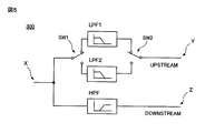
- FIG. 5 shows a diplexer circuit (a diplexer including a switchable low-pass filter) 300 disclosed in Patent Document 1.
- the diplexer circuit 300 includes three terminals X, Y, and Z.
- the diplexer circuit 300 includes a first low-pass filter LPF1, a second low-pass filter LPF2, and a high-pass filter HPF, each of which includes an inductor and a capacitor.
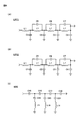
- FIG. 6A shows an equivalent circuit of the first low-pass filter LPF1.
- FIG. 6B shows an equivalent circuit of the second low-pass filter LPF2.
- FIG. 6C shows an equivalent circuit of the high-pass filter HPF.
- the diplexer circuit 300 includes a first switch SW1 and a second switch SW2 that are switched in conjunction with each other.
- the diplexer circuit 300 switches either the first low-pass filter LPF1 or the second low-pass filter LPF between the terminal X and the terminal Y by switching the first switch SW1 and the second switch SW2 in conjunction with each other. Connected. A high-pass filter HPF is always connected between the terminal X and the terminal Z.
- the terminal X is connected to a cable of a provider that provides the content.
- the terminal Y is connected to a transmission circuit (upstream processing circuit).
- the terminal Z is connected to a receiving circuit (downstream processing circuit).
- the diplexer circuit 300 selects one of the first low-pass filter LPF1 and the second low-pass filter LPF2 by interlockingly switching the first switch SW1 and the second switch SW2, and selects one of the two different frequencies. Transmission can be performed by frequency.
- a diplexer circuit capable of transmitting at two different frequencies was manufactured by the diplexer circuit 300 disclosed in Patent Document 1.
- the cutoff frequency of the first low-pass filter LPF1 was set to 42 MHz. Further, the cutoff frequency of the second low-pass filter LPF2 was set to 65 MHz. Further, the cutoff frequency of the high pass filter HPF was set to 88 MHz. These cut-off frequencies were determined by selecting the constants of the inductors and capacitors constituting each filter.
- SPDT Single-Pole-Double-Throw switches were used for the first switch SW1 and the second switch SW2, respectively.
- the first switch SW1 and the second switch SW2 are switched in conjunction with each other.
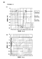
- FIG. 7A and 7B show frequency characteristics when the first low-pass filter LPF1 is connected between the first switch SW1 and the second switch SW2 of the diplexer circuit 300.
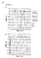
- FIG. 8A and 8B show frequency characteristics when the second low-pass filter LPF2 is connected between the first switch SW1 and the second switch SW2 of the diplexer circuit 300.
- FIG. 7A is a partially enlarged view of FIG. 7B
- FIG. 8A is a partially enlarged view of FIG. 8B.
- the first low-pass filter LPF1 when the first low-pass filter LPF1 is connected between the first switch SW1 and the second switch SW2 of the diplexer circuit 300, it is in the vicinity of 1.4 GHz in the passband of the high-pass filter HPF. Unnecessary attenuation D1 occurs. Further, as can be seen from FIG. 8B, when the second low-pass filter LPF2 is connected between the first switch SW1 and the second switch SW2 of the diplexer circuit 300, it is similarly within the passband of the high-pass filter HPF. An unnecessary attenuation D2 occurs in the vicinity of 1.4 GHz.
- the diplexer circuit of the present invention is a common terminal, a transmission terminal, a reception terminal, and a diplexer, and includes a first terminal. , A second terminal, a third terminal, a first low-pass filter, and a high-pass filter or a band-pass filter, the first low-pass filter being inserted between the first terminal and the second terminal, A high-pass filter or a band-pass filter inserted between the first and second terminals, a second low-pass filter, a third low-pass filter, and a first switch and a second switch that are switched in conjunction with each other,
- the first terminal of the diplexer is connected to the shared terminal
- the second terminal of the diplexer is connected to the first switch
- the third terminal of the diplexer is connected to the receiving terminal.
- a diplexer including a first low-pass filter and a high-pass filter or a band-pass filter is formed on one module substrate.
- the diplexer circuit of the present invention can be easily manufactured by using a diplexer module configured by a multilayer substrate or a diplexer module configured by mounting electronic components such as capacitors on the multilayer substrate.
- the first low pass filter of the diplexer includes a first inductor connected to the first terminal, a second inductor connected between the first inductor and the second terminal, and a first inductor and a second inductor.
- a T-type filter including a capacitor connected between the connection point and the ground is preferable. In this case, the pass characteristic required for the first low-pass filter can be easily formed by the T-type filter.
- a capacitor is connected in parallel with the second inductor, and an LC resonator is formed by the second inductor and the capacitor.
- this LC resonator With this LC resonator, the passband characteristics formed by the first lowpass filter and the second lowpass filter, and the passband characteristics formed by the first lowpass filter and the third lowpass filter, respectively, It can be improved to a better one.
- the resonance frequency of the LC resonator is provided in the pass band of the high-pass filter or the band-pass filter.
- the LC resonator causes the reception signal to interfere with the transmission circuit via the first low-pass filter and the second low-pass filter, or via the first low-pass filter and the third low-pass filter. This is because this can be suppressed.
- the cutoff frequency of the third low-pass filter is higher than the cutoff frequency of the second low-pass filter
- the third low-pass filter includes at least one LC resonator
- the resonance frequency of the LC resonator is high-pass. It is preferably provided within the passband of the filter or bandpass filter.
- the LC resonator can suppress the reception signal from interfering with the transmission circuit via the first low-pass filter and the third low-pass filter.
- the diplexer circuit module of the present invention can be configured on a module substrate made of ceramic, resin, or the like to produce a diplexer circuit module.
- the diplexer circuit according to the present invention includes two transmission filter circuits including a first low-pass filter and a second low-pass filter, and a transmission filter circuit including a first low-pass filter and a third low-pass filter. Although a transmission filter circuit is provided, a part of both is shared by the first low-pass filter, so that the number of electronic components necessary to manufacture a diplexer circuit is reduced.
- FIG. 1 is an equivalent circuit diagram showing a diplexer circuit 100 according to a first embodiment.
- 2A and 2B are graphs showing frequency characteristics of the diplexer circuit 100 when the second low-pass filter LPF2 is selected.
- FIG. 2A partially enlarges FIG. 2B.
- 3A and 3B are graphs showing the frequency characteristics of the diplexer circuit 100 when the third low-pass filter LPF3 is selected.
- FIG. 3A partially enlarges FIG. 3B.
- 6 is an equivalent circuit diagram showing a diplexer circuit 300 disclosed in Patent Document 1.
- FIG. FIG. 6A is an equivalent circuit diagram of the first low-pass filter LPF 1 of the diplexer circuit 300.
- FIG. 6B is an equivalent circuit diagram of the second low-pass filter LPF2 of the diplexer circuit 300.
- FIG. 6C is an equivalent circuit diagram of the high pass filter HPF of the diplexer circuit 300.
- FIGS. 7A and 7B are graphs showing the frequency characteristics of the diplexer circuit 300 when the first low-pass filter LPF1 is selected. Note that FIG. 7A partially enlarges FIG. 7B.
- FIGS. 8A and 8B are graphs showing frequency characteristics of the diplexer circuit 300 when the second low-pass filter LPF2 is selected. Note that FIG. 8A partially enlarges FIG. 8B.
- each embodiment shows an embodiment of the present invention by way of example, and the present invention is not limited to the content of the embodiment. Moreover, it is also possible to implement combining the content described in different embodiment, and the implementation content in that case is also included in this invention. Further, the drawings are for helping understanding of the embodiment, and may not be drawn strictly. For example, a drawn component or a dimensional ratio between the components may not match the dimensional ratio described in the specification. In addition, the constituent elements described in the specification may be omitted in the drawings or may be drawn with the number omitted.
- FIG. 1 shows an equivalent circuit of the diplexer circuit 100 according to the first embodiment.
- the diplexer circuit 100 includes a shared terminal X, a transmission terminal Y, and a reception terminal Z.
- the diplexer circuit 100 includes a diplexer DPLX.
- the diplexer DPLX includes a first terminal T1, a second terminal T2, a third terminal T3, a first low-pass filter LPF1, and a high-pass filter HPF.
- a first low-pass filter LPF1 is inserted between the first terminal T1 and the second terminal T2.
- a high-pass filter HPF is inserted between the first terminal T1 and the third terminal T3.
- the first low-pass filter LPF1 and the high-pass filter HPF are configured on one module substrate. Instead of the high pass filter HPF, a band pass filter BPF (not shown) may be used.
- the first low-pass filter LPF1 of the diplexer DPLX not only functions as a low-pass filter but also functions as a matching circuit between the first switch SW1 and the high-pass filter HPF.
- the diplexer circuit 100 includes a second low-pass filter LPF2 and a third low-pass filter LPF3.
- the diplexer circuit 100 includes a first switch SW1 and a second switch SW2 that are switched in conjunction with each other.
- the first switch SW1 and the second switch SW2 for example, SPDT (Single Pole Double Throw) switch is used.
- SPDT Single Pole Double Throw
- the first switch SW1 and the second switch SW2 are switched in conjunction with each other.
- the first terminal T1 of the diplexer DPLX is connected to the common terminal X.
- the second terminal T2 of the diplexer DPLX is connected to the first switch SW1.
- the third terminal T3 of the diplexer DPLX is connected to the reception terminal Z. Further, the second switch SW2 is connected to the transmission terminal Y.
- the diplexer circuit 100 switches the first switch SW1 and the second switch SW2 in conjunction with each other so that one of the second low-pass filter LPF2 and the third low-pass filter LPF3 is switched between the first switch SW1 and the second switch SW2. Alternatively connected between them.
- first low-pass filter LPF1 two inductors L1 (first inductor) and inductor L2 (second inductor) are connected in series, and a capacitor C1 is connected between a connection point between the inductor L1 and the inductor L2 and the ground. It is composed of connected T-type filters.
- a capacitor C2 is connected in parallel with the inductor L2, and the LC parallel resonator LC1 is formed by the inductor L2 and the capacitor C2.
- the LC series resonator LC9 is formed by the capacitor C22 and the inductor L12.
- An LC series resonator LC10 including an inductor L13 and a capacitor C23 is connected between a connection point between the capacitor C18 and the capacitor C19 and the ground.
- An LC series resonator LC11 including an inductor L14 and a capacitor C24 is connected between a connection point between the capacitor C19 and the capacitor C20 and the ground.
- An LC series resonator LC12 including an inductor L15 and a capacitor C25 is connected between a connection point between the capacitor C20 and the capacitor C21 and the ground.
- An LC series resonator LC13 including an inductor L16 and a capacitor C26 is connected between a connection point between the capacitor C21 and the capacitor C22 and the ground.
- An LC parallel resonator LC14 including an inductor L17 and a capacitor C27 is connected between a connection point between the inductor L12 and the third terminal T3 and the ground.
- the cut-off frequency of the high-pass filter HPF is set to 108 MHz by selecting the inductor and capacitor constants.
- the second low-pass filter LPF2 has five inductors L3 to L7 connected in series.
- An LC series resonator LC2 including an inductor L8 and a capacitor C3 is connected between a connection point between the inductor L3 and the inductor L4 and the ground.
- a capacitor C4 is connected between the connection point of the inductor L4 and the inductor L5 and the ground.
- a capacitor C5 is connected between the connection point of the inductor L5 and the inductor L6 and the ground.
- a capacitor C6 is connected between the connection point of the inductor L6 and the inductor L7 and the ground.
- a capacitor C7 is connected between the connection point of the inductor L7 and the second switch SW2 and the ground.
- a capacitor C8 is connected in parallel with the inductor L5, and an LC parallel resonator LC3 is formed by the inductor L5 and the capacitor C8.
- a capacitor C9 is connected in parallel with the inductor L6, and an LC parallel resonator LC4 is formed by the inductor L6 and the capacitor C9.
- a capacitor C10 is connected in parallel with the inductor L7, and an LC parallel resonator LC5 is formed by the inductor L7 and the capacitor C10.
- both of them become a low-pass filter having a cut-off frequency of 42 MHz.
- the third low-pass filter LPF3 has three inductors L9 to L11 connected in series.
- a capacitor C11 is connected between the connection point of the first switch SW1 and the inductor L9 and the ground.
- a capacitor C12 is connected between the connection point of the inductor L9 and the inductor L10 and the ground.
- a capacitor C13 is connected between the connection point of the inductor L10 and the inductor L11 and the ground.
- a capacitor C14 is connected between the connection point of the inductor L11 and the second switch SW2 and the ground.
- the third low-pass filter LPF3 has a capacitor C15 connected in parallel with the inductor L9, and an LC parallel resonator LC6 is formed by the inductor L9 and the capacitor C15.
- a capacitor C16 is connected in parallel with the inductor L10, and the LC parallel resonator LC7 is formed by the inductor L10 and the capacitor C16.
- a capacitor C17 is connected in parallel with the inductor L11, and the LC parallel resonator LC8 is formed by the inductor L11 and the capacitor C17.
- LC parallel resonator LC1 formed in the first low pass filter LPF1
- LC series resonator LC2 formed in the second low pass filter LPF2
- LC parallel resonator LC6 formed in the third low pass filter LPF3
- Table 1 shows the resonance frequencies of LC series resonators LC9 to LC13 and LC parallel resonator LC14 formed in LC8 and high-pass filter HPF.
- the resonance frequency of the LC parallel resonator LC1 formed in the first low-pass filter LPF is set to 133 MHz and is provided in the pass band (108 MHz to) of the high-pass filter HPF.
- the LC parallel resonator LC1 causes the received signal to pass through the first low-pass filter LPF1 and the second low-pass filter LPF2, or the first low-pass filter LPF1 and the third low-pass filter LPF3. Interference with the transmission circuit is suppressed.
- the third low-pass filter LPF3 having a cutoff frequency higher than that of the second low-pass filter LPF2 includes three LC parallel resonators LC6 to LC8, and the resonance frequencies thereof are 113 MHz to 187 MHz.
- the high pass filter HPF is provided in the pass band (108 MHz to).
- the diplexer circuit 100 connects the shared terminal X to the cable of the provider that provides the content, connects the transmission terminal Y to the transmission circuit, and connects the reception terminal Z to the reception circuit, thereby enabling DOCSIS. It can be used as a diplexer circuit compatible with both (registered trademark) 3.0 and DOCSIS 3.1.
- the first low-pass filter LPF1 and the second low-pass filter LPF2 have a cutoff frequency of 42 MHz.
- a low-pass filter is configured.
- the diplexer circuit 100 can perform transmission conforming to DOCSIS 3.0 by passing through this low-pass filter.
- the first low-pass filter LPF1 and the third low-pass filter LPF3 When the third low-pass filter LPF3 is connected between the first switch SW1 and the second switch SW2, the first low-pass filter LPF1 and the third low-pass filter LPF3 have a cutoff frequency of 85 MHz.
- a low-pass filter is configured.
- the diplexer circuit 100 can perform transmission conforming to DOCSIS 3.1 by passing through this low-pass filter.
- 2A and 2B show frequency characteristics when the second low-pass filter LPF2 is connected between the first switch SW1 and the second switch SW2 (based on DOCSIS3.0).
- 3A and 3B show frequency characteristics when the third low-pass filter LPF3 is connected between the first switch SW1 and the second switch SW2 (based on DOCSIS3.1).
- 2A is a partially enlarged view of FIG. 2B
- FIG. 3A is a partially enlarged view of FIG. 3B.
- either the second low-pass filter LPF2 or the third low-pass filter LPF3 is interposed between the first switch SW1 and the second switch SW2.
- unnecessary attenuation does not occur in the pass band of the high pass filter HPF. That is, in the diplexer circuit 100, since the first low-pass filter LPF1 functions as a matching circuit between the first switch SW1 and the high-pass filter HPF, unnecessary resonance is generated between the first switch SW1 and the high-pass filter HPF. It is considered that no unnecessary attenuation occurs in the pass band of the high pass filter HPF.
- the diplexer circuit 100 includes two transmission filter circuits including a first low-pass filter LPF1 and a second low-pass filter LPF2, and a transmission filter circuit including a first low-pass filter LPF1 and a third low-pass filter LPF3. Although a transmission filter circuit is provided, a part of both is shared by the first low-pass filter LPF1, so that the effect of reducing the number of necessary electronic components is also achieved.
- the diplexer circuit 100 If the diplexer circuit 100 according to the present embodiment is used, communication corresponding to both DOCSIS 3.0 and DOCSIS 3.1 versions can be performed.
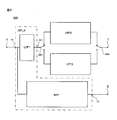
- FIG. 4 is a block diagram of a diplexer circuit 200 according to the second embodiment.
- the diplexer DPLX includes the high-pass filter HPF.
- the diplexer DPLX includes a band pass filter BPF instead of the high pass filter HPF.
- the other configuration of the diplexer circuit 200 is the same as that of the diplexer circuit 100 according to the first embodiment.
- the first low-pass filter LPF1 functions as a matching circuit between the first switch SW1 and the band-pass filter BPF, unnecessary resonance occurs between the first switch SW1 and the band-pass filter BPF. Thus, unnecessary attenuation does not occur in the pass band of the bandpass filter BPF.
- the diplexer circuits 100 and 200 according to the first embodiment and the second embodiment have been described above.
- the diplexer circuit of the present invention is not limited to the contents described above, and various modifications can be made in accordance with the spirit of the invention.
- each circuit configuration of the first low-pass filter LPF1, the second low-pass filter LPF2, the third low-pass filter LPF3, and the high-pass filter HPF is arbitrary, and is not limited to the above-described contents.
- Each cutoff frequency that is set is also arbitrary, and is not limited to the above-described content.
- DOCSIS version 3.0 and version 3.1 have been described as examples.
- the communication standard in which the diplexer circuit of the present invention is used is not limited to DOCSIS.
- it is not limited to version 3.0 and version 3.1.
Landscapes
- Engineering & Computer Science (AREA)
- Computer Networks & Wireless Communication (AREA)
- Signal Processing (AREA)
- Filters And Equalizers (AREA)
- Transceivers (AREA)
Abstract
ハイパスフィルタ(またはバンドパスフィルタ)の通過帯域内に発生する不要な減衰が抑制されたダイプレクサ回路を提供する。 共用端子Xと、送信端子Yと、受信端子Zと、ダイプレクサDPLXであって、第1端子T1と、第2端子T2と、第3端子T3と、第1ローパスフィルタLPF1と、ハイパスフィルタHPF(またはバンドパスフィルタBPF)とを備えたものと、第2ローパスフィルタLPF2と、第3ローパスフィルタLPF3と、連動して切り替えられる第1スイッチSW1および第2スイッチSW2と、を備え、第1スイッチSW1および第2スイッチSW2を連動して切り替えることにより、第2ローパスフィルタLPF2および第3ローパスフィルタLPF3のいずれか一方が、第1スイッチSW1と第2スイッチSW2との間に択一的に接続されるようにした。
Description
本発明は、複数のローパスフィルタと、ハイパスフィルタまたはバンドパスフィルタとを備え、複数のローパスフィルタを切り替えて使用するダイプレクサ回路に関し、さらに詳しくは、ハイパスフィルタまたはバンドパスフィルタの通過帯域内に発生する不要な減衰が抑制されたダイプレクサ回路に関する。
また、本発明は、1つのモジュール基板に、本発明のダイプレクサ回路を構成したダイプレクサ回路モジュールに関する。
ケーブルテレビの回線を利用した高速データ通信の規格として、DOCSIS(登録商標)(Data Over Cable Service Interface Specifications)が定められ、同規格によるデータ通信サービスが多くの国において採用されている。
DOCSISは、これまで数度にわたって改善がなされ、バージョンアップがなされてきた。また、今後も、バージョンアップが予定されている。
DOCSISのバージョンアップにおいては、通信周波数が変更される場合がある。
DOCSISは、バージョンアップにおいて通信周波数が変更される場合には、新バージョンの通信機器が、旧バージョンにおいても使用できること、言い換えれば、旧バージョンの通信周波数にも対応できることを義務付けている。すなわち、新しい通信機器が、旧バージョンが採用されているサービス地域においても、新バージョンが採用されているサービス地域においても、互換性をもって兼用できることを義務付けている。このため、DOCSISのように、1つの通信機器を使用して、複数の通信周波数で、双方向の通信を行いたい場合、外部からのアンテナやケーブルと、内部(室内)の通信配線とを繋ぐセットトップボックスに、最新バージョンのDOCSISや旧バージョンのDOCSISに対応した複数のフィルタを切り替えて用いるダイプレクサ回路を使用する場合がある。
そのようなダイプレクサ回路が、特許文献1(米国特許第7020186号公報)に開示されている。このダイプレクサ回路は、2つのローパスフィルタを切り替えて用いることにより、2つの異なる周波数での送信が可能になっている。
図5に、特許文献1に開示されたダイプレクサ回路(切り替え可能なローパスフィルタを備えたダイプレクサ)300を示す。
ダイプレクサ回路300は、3つの端子X、Y、Zを備える。
また、ダイプレクサ回路300は、それぞれ、インダクタとキャパシタとで構成された、第1ローパスフィルタLPF1と、第2ローパスフィルタLPF2と、ハイパスフィルタHPFを備える。図6(A)に、第1ローパスフィルタLPF1の等価回路を示す。図6(B)に、第2ローパスフィルタLPF2の等価回路を示す。図6(C)に、ハイパスフィルタHPFの等価回路を示す。
また、ダイプレクサ回路300は、連動して切り替えられる第1スイッチSW1と、第2スイッチSW2とを備える。
ダイプレクサ回路300は、第1スイッチSW1および第2スイッチSW2を連動して切り替えることにより、第1ローパスフィルタLPF1および第2ローパスフィルタLPFのいずれか一方が、端子Xと端子Yとの間に択一的に接続される。端子Xと端子Zとの間には、常時、ハイパスフィルタHPFが接続される。
ダイプレクサ回路300においては、端子Xを、コンテンツを提供する事業者などのケーブルに接続する。また、ダイプレクサ回路300においては、端子Yを、送信回路(アップストリーム・プロセッシング回路;upstream processing circuitry)に接続する。さらに、ダイプレクサ回路300においては、端子Zを、受信回路(ダウンストリーム・プロセッシング回路;downstream processing circuitry)に接続する。
ダイプレクサ回路300は、第1スイッチSW1および第2スイッチSW2を連動して切り替えることにより、第1ローパスフィルタLPF1および第2ローパスフィルタLPF2のいずれか一方を選択し、異なる2つの周波数のうちの一方の周波数により送信をおこなうことができる。
特許文献1に開示されたダイプレクサ回路300により、2つの異なる周波数で送信が可能なダイプレクサ回路を作製した。
具体的には、第1ローパスフィルタLPF1のカットオフ周波数を42MHzに設定した。また、第2ローパスフィルタLPF2のカットオフ周波数を65MHzに設定した。さらに、ハイパスフィルタHPFのカットオフ周波数を88MHzに設定した。これらのカットオフ周波数は、各フィルタを構成するインダクタおよびキャパシタの定数を選定することによりおこなった。
また、第1スイッチSW1および第2スイッチSW2には、それぞれ、SPDT(Single Pole Double Throw)スイッチを使用した。第1スイッチSW1と第2スイッチSW2とは、連動して切り替えがおこなわれる。
図7(A)、(B)に、ダイプレクサ回路300の第1スイッチSW1と第2スイッチSW2との間に、第1ローパスフィルタLPF1を接続した場合の周波数特性を示す。また、図8(A)、(B)に、ダイプレクサ回路300の第1スイッチSW1と第2スイッチSW2との間に、第2ローパスフィルタLPF2を接続した場合の周波数特性を示す。なお、図7(A)は図7(B)を部分的に拡大して示したもの、図8(A)は図8(B)を部分的に拡大して示したものである。
図7(B)から分かるように、ダイプレクサ回路300の第1スイッチSW1と第2スイッチSW2との間に第1ローパスフィルタLPF1を接続した場合、ハイパスフィルタHPFの通過帯域内の1.4GHz近傍に、不要な減衰D1が発生している。また、図8(B)から分かるように、ダイプレクサ回路300の第1スイッチSW1と第2スイッチSW2との間に第2ローパスフィルタLPF2を接続した場合も、同様に、ハイパスフィルタHPFの通過帯域内の1.4GHz近傍に、不要な減衰D2が発生している。
これらの不要な減衰D1、D2は、図5に示すX端子からみた入力インピーダンスと第1スイッチSW1が持つインピーダンスが異なることによるインピーダンス不整合による共振現象によるものである。なお、ダイプレクサ回路300のハイパスフィルタHPFが、バンドパスフィルタBPF(図示せず)に置換えられた場合にも、同様の問題が発生する。
特許文献1に開示されたダイプレクサ回路300は、ハイパスフィルタHPFの通過帯域内の1.4GHz近傍に、不要な減衰D1、D2が発生するため、DOCSIS3.1に準拠したシステムでは、事実上、2つの周波数で送信し得るダイプレクサ回路として使用することができなかった。
本発明は、上述した従来の問題を解決するためになされたものであり、その手段として本発明のダイプレクサ回路は、共用端子と、送信端子と、受信端子と、ダイプレクサであって、第1端子と、第2端子と、第3端子と、第1ローパスフィルタと、ハイパスフィルタまたはバンドパスフィルタとを備え、第1端子と第2端子との間に第1ローパスフィルタが挿入され、第1端子と第3端子との間にハイパスフィルタまたはバンドパスフィルタが挿入されたものと、第2ローパスフィルタと、第3ローパスフィルタと、連動して切り替えられる第1スイッチおよび第2スイッチと、を備え、ダイプレクサの第1端子が共用端子に接続され、ダイプレクサの第2端子が第1スイッチに接続され、ダイプレクサの第3端子が受信端子に接続され、第2スイッチが送信端子に接続され、第1スイッチおよび第2スイッチを連動して切り替えることにより、第2ローパスフィルタおよび第3ローパスフィルタのいずれか一方が、第1スイッチと第2スイッチとの間に択一的に接続されるものとした。
第1ローパスフィルタと、ハイパスフィルタまたはバンドパスフィルタとで構成されるダイプレクサが、1つのモジュール基板に形成されていることが好ましい。この場合には、多層基板で構成したダイプレクサモジュールや、多層基板にキャパシタなどの電子部品を実装して構成したダイプレクサモジュールを使用することにより、容易に本発明のダイプレクサ回路を作製することができる。
また、ダイプレクサの第1ローパスフィルタが、第1端子に接続された第1インダクタと、第1インダクタと第2端子との間に接続された第2インダクタと、第1インダクタと第2インダクタとの接続点とグランドとの間に接続されたキャパシタと、を備えたT型フィルタであることが好ましい。この場合には、T型フィルタにより、第1ローパスフィルタに要求される通過特性を容易に形成することができる。
また、上記第2インダクタと並列にキャパシタが接続され、第2インダクタとそのキャパシタとでLC共振器が形成されることが好ましい。この場合には、このLC共振器により、第1ローパスフィルタおよび第2ローパスフィルタにより形成される通過帯域特性、および、第1ローパスフィルタおよび第3ローパスフィルタにより形成される通過帯域特性を、それぞれ、より優れたものに改善することができる。
また、上記LC共振器の共振周波数が、ハイパスフィルタまたはバンドパスフィルタの通過帯域内に設けられていることが好ましい。この場合には、このLC共振器により、受信信号が、第1ローパスフィルタおよび第2ローパスフィルタを経由して、または、第1ローパスフィルタおよび第3ローパスフィルタを経由して、送信回路に混信することを抑制することができるからである。
さらに、第2ローパスフィルタのカットオフ周波数よりも、第3ローパスフィルタのカットオフ周波数が高く、第3ローパスフィルタは、少なくとも1個のLC共振器を備え、そのLC共振器の共振周波数が、ハイパスフィルタまたはバンドパスフィルタの通過帯域内に設けられていることが好ましい。この場合には、このLC共振器により、受信信号が、第1ローパスフィルタおよび第3ローパスフィルタを経由して、送信回路に混信することを抑制することができる。
本発明のダイプレクサ回路を、セラミックや樹脂などからなるモジュール基板に構成し、ダイプレクサ回路モジュールを作製することができる。
本発明のダイプレクサ回路は、第1スイッチと、ハイパスフィルタまたはバンドパスフィルタとの間の不要な共振が抑制され、ハイパスフィルタまたはバンドパスフィルタの通過帯域内に不要な減衰が発生しない。
また、本発明のダイプレクサ回路は、第1ローパスフィルタと第2ローパスフィルタとで構成される送信フィルタ回路と、第1ローパスフィルタと第3ローパスフィルタとで構成される送信フィルタ回路との、2つの送信フィルタ回路を備えるが、両者の一部分を、それぞれ、第1ローパスフィルタにより兼用しているため、ダイプレクサ回路を作製するのに必要な電子部品の個数が削減されている。
以下、図面とともに、本発明を実施するための形態について説明する。
なお、各実施形態は、本発明の実施の形態を例示的に示したものであり、本発明が実施形態の内容に限定されることはない。また、異なる実施形態に記載された内容を組合せて実施することも可能であり、その場合の実施内容も本発明に含まれる。また、図面は、実施形態の理解を助けるためのものであり、必ずしも厳密に描画されていない場合がある。たとえば、描画された構成要素ないし構成要素間の寸法の比率が、明細書に記載されたそれらの寸法の比率と一致していない場合がある。また、明細書に記載されている構成要素が、図面において省略されている場合や、個数を省略して描画されている場合などがある。
[第1実施形態]
図1に、第1実施形態にかかるダイプレクサ回路100の等価回路を示す。
図1に、第1実施形態にかかるダイプレクサ回路100の等価回路を示す。
ダイプレクサ回路100は、共用端子Xと、送信端子Yと、受信端子Zと、を備える。
また、ダイプレクサ回路100は、ダイプレクサDPLXを備える。ダイプレクサDPLXは、第1端子T1と、第2端子T2と、第3端子T3と、第1ローパスフィルタLPF1と、ハイパスフィルタHPFとを備える。ダイプレクサDPLXは、第1端子T1と第2端子T2との間に第1ローパスフィルタLPF1が挿入されている。また、ダイプレクサDPLXは、第1端子T1と第3端子T3との間にハイパスフィルタHPFが挿入されている。なお、ダイプレクサDPLXは、第1ローパスフィルタLPF1とハイパスフィルタHPFとが、1つのモジュール基板上に構成されている。なお、ハイパスフィルタHPFに代えて、バンドパスフィルタBPF(図示せず)を使用しても良い。
なお、ダイプレクサDPLXの第1ローパスフィルタLPF1は、ローパスフィルタとしての機能だけではなく、第1スイッチSW1とハイパスフィルタHPFとの整合回路としても機能している。
また、ダイプレクサ回路100は、第2ローパスフィルタLPF2と、第3ローパスフィルタLPF3とを備える。
さらに、ダイプレクサ回路100は、連動して切り替えられる第1スイッチSW1および第2スイッチSW2を備える。第1スイッチSW1および第2スイッチSW2には、たとえば、SPDT(Single Pole Double Throw)スイッチが使用される。第1スイッチSW1と第2スイッチSW2とは、連動して切り替えがおこなわれる。
ダイプレクサ回路100は、ダイプレクサDPLXの第1端子T1が、共用端子Xに接続されている。また、ダイプレクサDPLXの第2端子T2が、第1スイッチSW1に接続されている。また、ダイプレクサDPLXの第3端子T3が、受信端子Zに接続されている。さらに、第2スイッチSW2が、送信端子Yに接続されている。
ダイプレクサ回路100は、第1スイッチSW1および第2スイッチSW2を連動して切り替えることにより、第2ローパスフィルタLPF2および第3ローパスフィルタLPF3のいずれか一方が、第1スイッチSW1と第2スイッチSW2との間に択一的に接続される。
第1ローパスフィルタLPF1は、2個のインダクタL1(第1インダクタ)、インダクタL2(第2インダクタ)が直列に接続され、インダクタL1とインダクタL2との接続点と、グランドとの間にキャパシタC1が接続された、T型フィルタにより構成されている。また、インダクタL2と並列にキャパシタC2が接続されて、インダクタL2とキャパシタC2とでLC並列共振器LC1が形成されている。
ハイパスフィルタHPFは、5個のキャパシタC18~C22と、インダクタL12とが直列に接続されている。なお、キャパシタC22とインダクタL12とで、LC直列共振器LC9が形成されている。そして、キャパシタC18とキャパシタC19との接続点と、グランドとの間に、インダクタL13とキャパシタC23とで構成されるLC直列共振器LC10が接続されている。キャパシタC19とキャパシタC20との接続点と、グランドとの間に、インダクタL14とキャパシタC24とで構成されるLC直列共振器LC11が接続されている。キャパシタC20とキャパシタC21との接続点と、グランドとの間に、インダクタL15とキャパシタC25とで構成されるLC直列共振器LC12が接続されている。キャパシタC21とキャパシタC22との接続点と、グランドとの間に、インダクタL16とキャパシタC26とで構成されるLC直列共振器LC13が接続されている。インダクタL12と第3端子T3との接続点と、グランドとの間に、インダクタL17とキャパシタC27とで構成されるLC並列共振器LC14が接続されている。
ハイパスフィルタHPFは、インダクタおよびキャパシタの定数を選定することにより、カットオフ周波数が108MHzに設定されている。
第2ローパスフィルタLPF2は、5個のインダクタL3~L7が直列に接続されている。そして、インダクタL3とインダクタL4との接続点と、グランドとの間に、インダクタL8とキャパシタC3とで構成されるLC直列共振器LC2が接続されている。インダクタL4とインダクタL5との接続点と、グランドとの間にキャパシタC4が接続されている。インダクタL5とインダクタL6との接続点と、グランドとの間に、キャパシタC5が接続されている。インダクタL6とインダクタL7との接続点と、グランドとの間に、キャパシタC6が接続されている。インダクタL7と第2スイッチSW2との接続点と、グランドとの間に、キャパシタC7が接続されている。
また、第2ローパスフィルタLPF2は、インダクタL5と並列にキャパシタC8が接続されて、インダクタL5とキャパシタC8とでLC並列共振器LC3が形成されている。インダクタL6と並列にキャパシタC9が接続されて、インダクタL6とキャパシタC9とでLC並列共振器LC4が形成されている。インダクタL7と並列にキャパシタC10が接続されて、インダクタL7とキャパシタC10とでLC並列共振器LC5が形成されている。
第2ローパスフィルタLPF2は、第1ローパスフィルタと接続された場合、両者で42MHzのカットオフ周波数を備えたローパスフィルタになる。
第3ローパスフィルタLPF3は、3個のインダクタL9~L11が直列に接続されている。そして、第1スイッチSW1とインダクタL9との接続点と、グランドとの間に、キャパシタC11が接続されている。インダクタL9とインダクタL10との接続点と、グランドとの間にキャパシタC12が接続されている。インダクタL10とインダクタL11との接続点と、グランドとの間にキャパシタC13が接続されている。インダクタL11と第2スイッチSW2との接続点と、グランドとの間に、キャパシタC14が接続されている。
また、第3ローパスフィルタLPF3は、インダクタL9と並列にキャパシタC15が接続されて、インダクタL9とキャパシタC15とでLC並列共振器LC6が形成されている。インダクタL10と並列にキャパシタC16が接続されて、インダクタL10とキャパシタC16とでLC並列共振器LC7が形成されている。インダクタL11と並列にキャパシタC17が接続されて、インダクタL11とキャパシタC17とでLC並列共振器LC8が形成されている。
第3ローパスフィルタLPF3は、第1ローパスフィルタと接続された場合、両者で85MHzのカットオフ周波数を備えたローパスフィルタになる。
第1ローパスフィルタLPF1に形成したLC並列共振器LC1、第2ローパスフィルタLPF2に形成したLC直列共振器LC2、LC並列共振器LC3~LC5、第3ローパスフィルタLPF3に形成したLC並列共振器LC6~LC8、ハイパスフィルタHPFに形成したLC直列共振器LC9~LC13、LC並列共振器LC14の、それぞれの共振周波数を表1に示す。

また、ダイプレクサ回路100においては、第2ローパスフィルタLPF2に比べてカットオフ周波数が高い第3ローパスフィルタLPF3が、3個のLC並列共振器LC6~LC8を備え、それらの共振周波数を113MHz~187MHzとして、ハイパスフィルタHPFの通過帯域(108MHz~)内に設けている。この結果、ダイプレクサ回路100においては、LC並列共振器LC6~LC8により、受信信号が、第1ローパスフィルタLPF1および第3ローパスフィルタLPF3を経由して、送信回路に混信することが抑制されている。
本実施形態にかかるダイプレクサ回路100は、共用端子Xを、コンテンツを提供する事業者のケーブルに接続し、送信端子Yを送信回路に接続し、受信端子Zを受信回路に接続することにより、DOCSIS(登録商標)3.0とDOCSIS3.1の両方に対応したダイプレクサ回路として使用することができる。
すなわち、第1スイッチSW1と第2スイッチSW2との間に、第2ローパスフィルタLPF2が接続された場合には、第1ローパスフィルタLPF1と第2ローパスフィルタLPF2とで、42MHzのカットオフ周波数を備えたローパスフィルタが構成される。ダイプレクサ回路100は、このローパスフィルタを経由することにより、DOCSIS3.0に準拠した送信をおこなうことができる。
また、第1スイッチSW1と第2スイッチSW2との間に、第3ローパスフィルタLPF3が接続された場合には、第1ローパスフィルタLPF1と第3ローパスフィルタLPF3とで、85MHzのカットオフ周波数を備えたローパスフィルタが構成される。ダイプレクサ回路100は、このローパスフィルタを経由することにより、DOCSIS3.1に準拠した送信をおこなうことができる。
図2(A)、(B)に、第1スイッチSW1と第2スイッチSW2との間に、第2ローパスフィルタLPF2を接続した場合(DOCSIS3.0に準拠)の周波数特性を示す。また、図3(A)、(B)に、第1スイッチSW1と第2スイッチSW2との間に、第3ローパスフィルタLPF3を接続した場合(DOCSIS3.1に準拠)の周波数特性を示す。なお、図2(A)は図2(B)を部分的に拡大して示したもの、図3(A)は図3(B)を部分的に拡大して示したものである。
図2(B)、図3(B)から分かるように、ダイプレクサ回路100においては、第1スイッチSW1と第2スイッチSW2との間に、第2ローパスフィルタLPF2、第3ローパスフィルタLPF3のいずれを接続した場合においても、ハイパスフィルタHPFの通過帯域内に、不要な減衰は発生していない。すなわち、ダイプレクサ回路100においては、第1ローパスフィルタLPF1が、第1スイッチSW1とハイパスフィルタHPFと間の整合回路として機能しているため、第1スイッチSW1とハイパスフィルタHPFとの間に不要な共振が発生せず、ハイパスフィルタHPFの通過帯域内に不要な減衰が発生していないものと考えられる。
ダイプレクサ回路100は、第1ローパスフィルタLPF1と第2ローパスフィルタLPF2とで構成される送信フィルタ回路と、第1ローパスフィルタLPF1と第3ローパスフィルタLPF3とで構成される送信フィルタ回路との、2つの送信フィルタ回路を備えているが、両者の一部分を、それぞれ、第1ローパスフィルタLPF1により兼用しているため、必要な電子部品の個数を削減するという効果も奏している。
本実施形態にかかるダイプレクサ回路100を使用すれば、DOCSIS3.0とDOCSIS3.1の両方のバージョンに対応した通信をおこなうことができる。
[第2実施形態]
図4に、第2実施形態にかかるダイプレクサ回路200のブロック図を示す。
図4に、第2実施形態にかかるダイプレクサ回路200のブロック図を示す。
第1実施形態にかかるダイプレクサ回路100では、ダイプレクサDPLXが、ハイパスフィルタHPFを備えていた。
第2実施形態にかかるダイプレクサ回路200は、ハイパスフィルタHPFに代えて、ダイプレクサDPLXが、バンドパスフィルタBPFを備えたものとした。ダイプレクサ回路200の他の構成は、第1実施形態にかかるダイプレクサ回路100と同じにした。
ダイプレクサ回路200においても、第1ローパスフィルタLPF1が、第1スイッチSW1とバンドパスフィルタBPFと間の整合回路として機能するため、第1スイッチSW1とバンドパスフィルタBPFとの間に不要な共振が発生せず、バンドパスフィルタBPFの通過帯域内に不要な減衰が発生しない。
以上、第1実施形態、第2実施形態にかかるダイプレクサ回路100、200について説明した。しかしながら、本発明のダイプレクサ回路が上述した内容に限定されることはなく、発明の趣旨に沿って、種々の変形をなすことができる。
たとえば、第1ローパスフィルタLPF1、第2ローパスフィルタLPF2、第3ローパスフィルタLPF3、ハイパスフィルタHPF(あるいはバンドパスフィルタBPF)の各回路構成は任意であり、上述した内容には限定されない。また、設定される各カットオフ周波数も任意であり、上述した内容には限定されない。
また、実施形態においては、DOCSISのバージョン3.0およびバージョン3.1を例にとって説明したが、本発明のダイプレクサ回路が使用される通信規格がDOCSISに限定されることはない。また、DOCSISに使用される場合であっても、バージョン3.0およびバージョン3.1に限定されることはない。
X・・・共用端子
Y・・・送信端子
Z・・・受信端子
DPLX・・・ダイプレクサ
T1・・・第1端子
T2・・・第2端子
T3・・・第3端子
LPF1・・・第1ローパスフィルタ
HPF・・・ハイパスフィルタ
BPF・・・バンドパスフィルタ
LPF2・・・第2ローパスフィルタ
LPF3・・・第3ローパスフィルタ
SW1・・・第1スイッチ
SW2・・・第2スイッチ
Y・・・送信端子
Z・・・受信端子
DPLX・・・ダイプレクサ
T1・・・第1端子
T2・・・第2端子
T3・・・第3端子
LPF1・・・第1ローパスフィルタ
HPF・・・ハイパスフィルタ
BPF・・・バンドパスフィルタ
LPF2・・・第2ローパスフィルタ
LPF3・・・第3ローパスフィルタ
SW1・・・第1スイッチ
SW2・・・第2スイッチ
Claims (7)
- 共用端子と、
送信端子と、
受信端子と、
第1端子と、第2端子と、第3端子と、第1ローパスフィルタと、ハイパスフィルタまたはバンドパスフィルタとを備え、前記第1端子と前記第2端子との間に前記第1ローパスフィルタが挿入され、前記第1端子と前記第3端子との間に前記ハイパスフィルタまたは前記バンドパスフィルタが挿入されたダイプレクサと、
第2ローパスフィルタと、
第3ローパスフィルタと、
連動して切り替えられる第1スイッチおよび第2スイッチと、を備え、
前記ダイプレクサの前記第1端子が、前記共用端子に接続され、
前記ダイプレクサの前記第2端子が、前記第1スイッチに接続され、
前記ダイプレクサの前記第3端子が、前記受信端子に接続され、
前記第2スイッチが、前記送信端子に接続され、
前記第1スイッチおよび前記第2スイッチを連動して切り替えることにより、前記第2ローパスフィルタおよび前記第3ローパスフィルタのいずれか一方が、前記第1スイッチと前記第2スイッチとの間に択一的に接続されるダイプレクサ回路。 - 前記第1ローパスフィルタと、前記ハイパスフィルタまたは前記バンドパスフィルタとで構成される前記ダイプレクサが、1つのモジュール基板で形成されている、請求項1に記載されたダイプレクサ回路。
- 前記ダイプレクサの前記第1ローパスフィルタが、前記第1端子に接続された第1インダクタと、前記第1インダクタと前記第2端子との間に接続された第2インダクタと、前記第1インダクタと前記第2インダクタとの接続点とグランドとの間に接続されたキャパシタと、を備えたT型フィルタからなる、請求項1または2に記載されたダイプレクサ回路。
- 前記第2インダクタと並列にキャパシタが接続され、前記第2インダクタと当該キャパシタとでLC共振器が形成された、請求項3に記載されたダイプレクサ回路。
- 前記LC共振器の共振周波数が、前記ハイパスフィルタまたは前記バンドパスフィルタの通過帯域内に設けられている、請求項4に記載されたダイプレクサ回路。
- 前記第2ローパスフィルタのカットオフ周波数よりも、前記第3ローパスフィルタのカットオフ周波数が高く、
前記第3ローパスフィルタは、少なくとも1個のLC共振器を備え、当該LC共振器の共振周波数が、前記ハイパスフィルタまたは前記バンドパスフィルタの通過帯域内に設けられている、請求項1ないし5のいずれか1項に記載された、ダイプレクサ回路。 - 1つのモジュール基板に、請求項1ないし6のいずれか1項に記載されたダイプレクサ回路が構成されたダイプレクサ回路モジュール。
Applications Claiming Priority (2)
| Application Number | Priority Date | Filing Date | Title |
|---|---|---|---|
| JP2015253378 | 2015-12-25 | ||
| JP2015-253378 | 2015-12-25 |
Publications (1)
| Publication Number | Publication Date |
|---|---|
| WO2017110723A1 true WO2017110723A1 (ja) | 2017-06-29 |
Family
ID=59090301
Family Applications (1)
| Application Number | Title | Priority Date | Filing Date |
|---|---|---|---|
| PCT/JP2016/087736 Ceased WO2017110723A1 (ja) | 2015-12-25 | 2016-12-19 | ダイプレクサ回路およびダイプレクサ回路モジュール |
Country Status (2)
| Country | Link |
|---|---|
| TW (1) | TWI601379B (ja) |
| WO (1) | WO2017110723A1 (ja) |
Cited By (5)
| Publication number | Priority date | Publication date | Assignee | Title |
|---|---|---|---|---|
| CN111865350A (zh) * | 2019-04-05 | 2020-10-30 | 三星电机株式会社 | 前端模块 |
| US11387556B2 (en) | 2019-04-05 | 2022-07-12 | Samsung Electro-Mechanics Co., Ltd. | Frontend module |
| CN114884485A (zh) * | 2021-02-05 | 2022-08-09 | 天津威盛电子有限公司 | 复用器 |
| CN114928342A (zh) * | 2022-06-07 | 2022-08-19 | 江南大学 | 高隔离度低损耗集成无源微型双工器及其应用 |
| CN116260417A (zh) * | 2023-05-16 | 2023-06-13 | 成都频岢微电子有限公司 | 一种单谐振器滤波器、多谐振器滤波器和射频前端模组 |
Citations (5)
| Publication number | Priority date | Publication date | Assignee | Title |
|---|---|---|---|---|
| US20030022631A1 (en) * | 2001-07-13 | 2003-01-30 | Rhodes Robert Andrew | Multi-mode bidirectional communications device including a diplexer having a switchable notch filter |
| JP2003209454A (ja) * | 2001-11-12 | 2003-07-25 | Matsushita Electric Ind Co Ltd | ダイプレクサ並びにそれを用いた高周波スイッチ及びアンテナ共用器 |
| US7020186B2 (en) * | 2001-07-13 | 2006-03-28 | Thomson Licensing | Multi-mode bi-directional communications device including a diplexer having switchable low pass filters |
| JP2006128881A (ja) * | 2004-10-27 | 2006-05-18 | Kyocera Corp | ダイプレクサ |
| JP2006332980A (ja) * | 2005-05-25 | 2006-12-07 | Alps Electric Co Ltd | トリプレクサ回路 |
Family Cites Families (5)
| Publication number | Priority date | Publication date | Assignee | Title |
|---|---|---|---|---|
| US6765456B2 (en) * | 2001-12-17 | 2004-07-20 | Oki Electric Industry Co., Ltd. | Surface acoustic wave duplexer and portable communication device using the same |
| US20070030095A1 (en) * | 2005-08-05 | 2007-02-08 | Mitsutaka Hikita | Antenna duplexer and wireless terminal using the same |
| JP5360163B2 (ja) * | 2011-08-22 | 2013-12-04 | 株式会社村田製作所 | 高周波フロントエンドモジュール |
| US8824976B2 (en) * | 2012-04-11 | 2014-09-02 | Qualcomm Incorporated | Devices for switching an antenna |
| TWI520552B (zh) * | 2014-09-01 | 2016-02-01 | 鋐寶科技股份有限公司 | 可切換式雙工器 |
-
2016
- 2016-10-11 TW TW105132724A patent/TWI601379B/zh active
- 2016-12-19 WO PCT/JP2016/087736 patent/WO2017110723A1/ja not_active Ceased
Patent Citations (5)
| Publication number | Priority date | Publication date | Assignee | Title |
|---|---|---|---|---|
| US20030022631A1 (en) * | 2001-07-13 | 2003-01-30 | Rhodes Robert Andrew | Multi-mode bidirectional communications device including a diplexer having a switchable notch filter |
| US7020186B2 (en) * | 2001-07-13 | 2006-03-28 | Thomson Licensing | Multi-mode bi-directional communications device including a diplexer having switchable low pass filters |
| JP2003209454A (ja) * | 2001-11-12 | 2003-07-25 | Matsushita Electric Ind Co Ltd | ダイプレクサ並びにそれを用いた高周波スイッチ及びアンテナ共用器 |
| JP2006128881A (ja) * | 2004-10-27 | 2006-05-18 | Kyocera Corp | ダイプレクサ |
| JP2006332980A (ja) * | 2005-05-25 | 2006-12-07 | Alps Electric Co Ltd | トリプレクサ回路 |
Cited By (8)
| Publication number | Priority date | Publication date | Assignee | Title |
|---|---|---|---|---|
| CN111865350A (zh) * | 2019-04-05 | 2020-10-30 | 三星电机株式会社 | 前端模块 |
| CN111865350B (zh) * | 2019-04-05 | 2021-12-17 | 三星电机株式会社 | 前端模块 |
| US11387556B2 (en) | 2019-04-05 | 2022-07-12 | Samsung Electro-Mechanics Co., Ltd. | Frontend module |
| CN114884485A (zh) * | 2021-02-05 | 2022-08-09 | 天津威盛电子有限公司 | 复用器 |
| CN114928342A (zh) * | 2022-06-07 | 2022-08-19 | 江南大学 | 高隔离度低损耗集成无源微型双工器及其应用 |
| CN114928342B (zh) * | 2022-06-07 | 2024-02-06 | 江南大学 | 高隔离度低损耗集成无源微型双工器及其应用 |
| CN116260417A (zh) * | 2023-05-16 | 2023-06-13 | 成都频岢微电子有限公司 | 一种单谐振器滤波器、多谐振器滤波器和射频前端模组 |
| CN116260417B (zh) * | 2023-05-16 | 2023-07-11 | 成都频岢微电子有限公司 | 一种单谐振器滤波器、多谐振器滤波器和射频前端模组 |
Also Published As
| Publication number | Publication date |
|---|---|
| TWI601379B (zh) | 2017-10-01 |
| TW201724735A (zh) | 2017-07-01 |
Similar Documents
| Publication | Publication Date | Title |
|---|---|---|
| US10079587B2 (en) | Phase shifter, impedance matching circuit, multi/demultiplexer, and communication terminal apparatus | |
| JP5794365B2 (ja) | ケーブルおよび通信装置 | |
| CN101075695B (zh) | 半导体装置互连单元、半导体装置以及高频模块 | |
| US11956069B2 (en) | Multiplexer, filter, and communication device | |
| WO2017110723A1 (ja) | ダイプレクサ回路およびダイプレクサ回路モジュール | |
| JP4952716B2 (ja) | 高周波部品 | |
| JP4525826B2 (ja) | 高周波部品 | |
| US10110194B2 (en) | Variable filter circuit, RF front end circuit and communication device | |
| JP2013062556A (ja) | マルチプレクサ | |
| US10439582B2 (en) | Variable-frequency LC filter, high-frequency frontend module, and communication apparatus | |
| JP6365776B2 (ja) | 高周波フロントエンド回路 | |
| WO2012172909A1 (ja) | 分波器 | |
| JP2017503401A (ja) | フロントエンド回路およびフロントエンド回路の動作の方法 | |
| JP6352418B2 (ja) | Rfアンテナスイッチおよびこのアンテナスイッチの作動方法 | |
| US9007145B2 (en) | High-frequency signal balancing multiplexer | |
| JP2008271187A (ja) | 分波回路 | |
| JP7846525B2 (ja) | フィルタ、マルチプレクサおよび通信用モジュール | |
| TWI638540B (zh) | Duplexer module with switch and duplexer module | |
| JP7579186B2 (ja) | バンドエリミネーションフィルタ | |
| JP2011015064A (ja) | ダイプレクサ回路 | |
| JP2013118591A (ja) | フィルタ回路 | |
| JP2007013849A (ja) | ノッチ付バンドパスフィルタ |
Legal Events
| Date | Code | Title | Description |
|---|---|---|---|
| 121 | Ep: the epo has been informed by wipo that ep was designated in this application |
Ref document number: 16878612 Country of ref document: EP Kind code of ref document: A1 |
|
| NENP | Non-entry into the national phase |
Ref country code: DE |
|
| 122 | Ep: pct application non-entry in european phase |
Ref document number: 16878612 Country of ref document: EP Kind code of ref document: A1 |
|
| NENP | Non-entry into the national phase |
Ref country code: JP |