WO2017104753A1 - 超電導線材及び超電導コイル - Google Patents
超電導線材及び超電導コイル Download PDFInfo
- Publication number
- WO2017104753A1 WO2017104753A1 PCT/JP2016/087404 JP2016087404W WO2017104753A1 WO 2017104753 A1 WO2017104753 A1 WO 2017104753A1 JP 2016087404 W JP2016087404 W JP 2016087404W WO 2017104753 A1 WO2017104753 A1 WO 2017104753A1
- Authority
- WO
- WIPO (PCT)
- Prior art keywords
- wire
- superconducting
- current
- coil
- groove
- Prior art date
- Legal status (The legal status is an assumption and is not a legal conclusion. Google has not performed a legal analysis and makes no representation as to the accuracy of the status listed.)
- Ceased
Links
Images



Classifications
-
- H—ELECTRICITY
- H01—ELECTRIC ELEMENTS
- H01B—CABLES; CONDUCTORS; INSULATORS; SELECTION OF MATERIALS FOR THEIR CONDUCTIVE, INSULATING OR DIELECTRIC PROPERTIES
- H01B12/00—Superconductive or hyperconductive conductors, cables, or transmission lines
- H01B12/02—Superconductive or hyperconductive conductors, cables, or transmission lines characterised by their form
- H01B12/06—Films or wires on bases or cores
-
- H—ELECTRICITY
- H01—ELECTRIC ELEMENTS
- H01B—CABLES; CONDUCTORS; INSULATORS; SELECTION OF MATERIALS FOR THEIR CONDUCTIVE, INSULATING OR DIELECTRIC PROPERTIES
- H01B13/00—Apparatus or processes specially adapted for manufacturing conductors or cables
- H01B13/0036—Details
-
- H—ELECTRICITY
- H01—ELECTRIC ELEMENTS
- H01F—MAGNETS; INDUCTANCES; TRANSFORMERS; SELECTION OF MATERIALS FOR THEIR MAGNETIC PROPERTIES
- H01F27/00—Details of transformers or inductances, in general
- H01F27/28—Coils; Windings; Conductive connections
- H01F27/2871—Pancake coils
-
- H—ELECTRICITY
- H01—ELECTRIC ELEMENTS
- H01F—MAGNETS; INDUCTANCES; TRANSFORMERS; SELECTION OF MATERIALS FOR THEIR MAGNETIC PROPERTIES
- H01F6/00—Superconducting magnets; Superconducting coils
- H01F6/06—Coils, e.g. winding, insulating, terminating or casing arrangements therefor
-
- H—ELECTRICITY
- H02—GENERATION; CONVERSION OR DISTRIBUTION OF ELECTRIC POWER
- H02H—EMERGENCY PROTECTIVE CIRCUIT ARRANGEMENTS
- H02H7/00—Emergency protective circuit arrangements specially adapted for specific types of electric machines or apparatus or for sectionalised protection of cable or line systems, and effecting automatic switching in the event of an undesired change from normal working conditions
- H02H7/001—Emergency protective circuit arrangements specially adapted for specific types of electric machines or apparatus or for sectionalised protection of cable or line systems, and effecting automatic switching in the event of an undesired change from normal working conditions for superconducting apparatus, e.g. coils, lines, machines
-
- H—ELECTRICITY
- H10—SEMICONDUCTOR DEVICES; ELECTRIC SOLID-STATE DEVICES NOT OTHERWISE PROVIDED FOR
- H10N—ELECTRIC SOLID-STATE DEVICES NOT OTHERWISE PROVIDED FOR
- H10N60/00—Superconducting devices
- H10N60/01—Manufacture or treatment
- H10N60/0268—Manufacture or treatment of devices comprising copper oxide
- H10N60/0296—Processes for depositing or forming copper oxide superconductor layers
- H10N60/0576—Processes for depositing or forming copper oxide superconductor layers characterised by the substrate
-
- H—ELECTRICITY
- H10—SEMICONDUCTOR DEVICES; ELECTRIC SOLID-STATE DEVICES NOT OTHERWISE PROVIDED FOR
- H10N—ELECTRIC SOLID-STATE DEVICES NOT OTHERWISE PROVIDED FOR
- H10N60/00—Superconducting devices
- H10N60/20—Permanent superconducting devices
- H10N60/203—Permanent superconducting devices comprising high-Tc ceramic materials
-
- H—ELECTRICITY
- H01—ELECTRIC ELEMENTS
- H01F—MAGNETS; INDUCTANCES; TRANSFORMERS; SELECTION OF MATERIALS FOR THEIR MAGNETIC PROPERTIES
- H01F6/00—Superconducting magnets; Superconducting coils
- H01F6/02—Quenching; Protection arrangements during quenching
-
- Y—GENERAL TAGGING OF NEW TECHNOLOGICAL DEVELOPMENTS; GENERAL TAGGING OF CROSS-SECTIONAL TECHNOLOGIES SPANNING OVER SEVERAL SECTIONS OF THE IPC; TECHNICAL SUBJECTS COVERED BY FORMER USPC CROSS-REFERENCE ART COLLECTIONS [XRACs] AND DIGESTS
- Y02—TECHNOLOGIES OR APPLICATIONS FOR MITIGATION OR ADAPTATION AGAINST CLIMATE CHANGE
- Y02E—REDUCTION OF GREENHOUSE GAS [GHG] EMISSIONS, RELATED TO ENERGY GENERATION, TRANSMISSION OR DISTRIBUTION
- Y02E40/00—Technologies for an efficient electrical power generation, transmission or distribution
- Y02E40/60—Superconducting electric elements or equipment; Power systems integrating superconducting elements or equipment
Definitions
- the present invention relates to a superconducting wire and a superconducting coil in which the superconducting wire is wound in a coil shape, for example, a spiral shape or a spiral shape.
- the first reason is that the electric power consumed by the AC loss is converted into heat, which raises the temperature of superconducting equipment that requires cryogenic cooling.
- the ratio of the AC loss of the superconducting coil to the power consumption of the entire system is only small.
- it is necessary to raise the capacity of the cooling mechanism, and as a result, the introduction cost and running cost of the cooling mechanism become high. This is a serious problem from a practical point of view.
- the second reason is that the AC loss is larger in a device using superconductivity than in a device using a normal conductor.
- Alternating current loss such as hysteresis loss (so-called iron loss) and eddy current loss (so-called copper loss) also exists in equipment using a normal conductor (motor, etc.).
- the superconductor itself causes hysteresis loss and similar AC loss.
- the electrical conductivity literally increases by orders of magnitude, and eddy current loss may increase proportionally. The amount of loss is definitely larger than that of normal conductor devices.
- a superconducting wire having a flat cross-sectional shape such as a REBCO wire expected to be applied as a high-temperature superconducting (HTS) wire has a problem that hysteresis loss is particularly large. This is derived from the shape of the superconducting layer constituting the superconducting wire, which is a flat cross-sectional shape, in other words, a wide and tape-like shape.
- superconducting wires such as Nb-based and Bi-based superconducting regions are composed of a plurality of filaments (thin wires), and hysteresis loss hardly occurs.
- Patent Document 1 discloses that a superconducting thin film constituting a tape-type high-temperature superconducting wire is divided into a plurality of narrow superconducting thin film portions, and the divided superconducting thin film portions are electrically separated from each other, thereby providing hysteresis. A method for reducing loss is described.
- the above method has the following problems. That is, when manufacturing a wire, a defective part having a lower critical current than others may be locally formed for reasons such as contamination of the substrate or sudden anisotropy.
- the critical current is a current that generates a constant voltage per length of the superconducting wire. Specifically, it is a current that generates a voltage of 1 ⁇ V per 1 cm length, for example. If this defect part is small, more specifically, if the extent of the defect part in the wire width direction is sufficiently smaller than the width of the wire, the influence of the whole wire is limited.
- Patent Document 2 In order to overcome the weaknesses in the invention described in Patent Document 1 described above, in Patent Document 2, the divided lines as described in Patent Document 1 are not completely insulated but divided. A technique is described in which a certain amount of electrical conduction is allowed by filling the groove with metal.
- a superconducting wire is divided into a plurality of lines by a plurality of parallel grooves obliquely extending in the longitudinal direction of the wire, and each divided line is zigzag meandered in the wire. It is described that a reduction in shielding current and hysteresis loss is achieved by realizing dislocation between lines.
- An object of the present invention has been made in view of the above-described problems, and is capable of reducing hysteresis loss while preventing a decrease in critical current and suppressing heat generation, and a superconducting wire having a flat cross-sectional shape and the superconducting material.
- An object of the present invention is to provide a superconducting coil using a wire.
- the superconducting wire according to the first aspect of the present invention is a superconducting wire having a flat cross-sectional shape, and the region on at least one end side in the wire width direction is other than the region on the at least one end side.
- a voltage is generated at a lower current density compared to the region, or a higher voltage is generated at the same current density.
- how much voltage is generated at a certain current density in a certain region of the wire is determined by, for example, digging a groove so as to electrically insulate the superconducting part in the region from the superconducting part outside the region, and It is possible to know by measuring a voltage generated at that time by applying a constant current to the capacitor.
- the first aspect of the present invention by providing a mechanism that generates a voltage at a low current density in at least one of the end-side regions, formation of a shielding current band that becomes a source of hysteresis loss is inhibited. Hysteresis loss can be reduced while avoiding a decrease in critical current.
- the superconducting wire according to the second aspect of the present invention is a superconducting wire having a flat cross-sectional shape, and the superconducting layer of the superconducting wire has a length in the wire width direction from one or both ends in the wire width direction. A groove extending obliquely and terminating without reaching the other end is provided, and the groove is filled with metal.
- the second aspect of the present invention by providing a groove extending obliquely from one end or both ends in the wire width direction with respect to the wire longitudinal direction and terminating without reaching the other end, it becomes a source of hysteresis loss. Since the formation of the shielding current band is hindered, the hysteresis loss can be reduced while avoiding the decrease in the critical current.
- the superconducting wire according to the third aspect of the present invention is characterized in that, in the second aspect, an average value of the lengths of the grooves differs depending on a position in the longitudinal direction of the wire.
- the superconducting wire according to the fifth aspect of the present invention is a superconducting wire having a flat cross-sectional shape, and the critical current density in the region on at least one end side in the wire width direction is the at least one end side. It is characterized by being not more than half of the maximum critical current density in a region other than the above region.
- the critical current density in the wire can be measured by digging a groove that insulates the superconducting portion as described above, and can also be known by measuring the distribution of magnetic flux changes when an external magnetic field is applied.
- the critical current density on the at least one end side is lower than the critical current density on a region other than the region on the at least one end side. It has such a gradient current distribution of critical current values.
- the shielding current band that becomes a source of hysteresis loss by having a gradient distribution of the critical current that reduces the critical current density on at least one end side. Therefore, hysteresis loss can be reduced while avoiding a decrease in critical current.
- the superconducting wire of the present invention described above is suitable for constituting a superconducting coil in any aspect.
- the present invention it is possible to reduce the hysteresis loss while avoiding the decrease of the critical current, and to suppress the heat generation.
- FIG. 1 is a cross-sectional view showing a laminated structure of REBCO wires.
- FIG. 2 is a perspective view showing a double pancake coil made of a high-temperature superconducting wire.
- FIG. 3 is a diagram for explaining a mechanism for generating hysteresis loss in the superconducting coil.
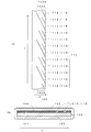
- FIG. 4 is a view showing a high-temperature superconducting wire according to the first embodiment to which the present invention is applied.
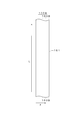
- FIG. 5 is a view showing a high-temperature superconducting wire according to the second embodiment to which the present invention is applied.
- FIG. 6 is a diagram showing a change in the residual ratio of critical current according to the position in the wire width direction in the high-temperature superconducting wire according to the second example.
- the REBCO wire 100 shown in FIG. 1 is obtained by sequentially laminating an intermediate layer 102, a REBCO superconducting layer 103, and a protective layer 104 on one surface of a substrate 101, and further covering the periphery of the laminate with a stabilization layer 105. It is.
- a nickel-base alloy represented by Hastelloy (registered trademark), stainless steel, or the like is used for the substrate 101.
- the intermediate layer 102 is a layer serving as a base for the superconducting layer 103, and physical characteristic values such as a coefficient of thermal expansion and a lattice constant indicate intermediate values between the substrate 101 and the superconductor constituting the REBCO superconducting layer 103.
- the REBCO superconducting layer 103 is made of a high-temperature superconductor made of a rare earth atom such as yttrium, a copper oxide, or the like.
- the protective layer 104 is a layer that covers the surface of the superconducting layer 103, and for example, silver is used.
- the stabilization layer 105 is a layer that covers the periphery of the laminate in which the intermediate layer 102, the REBCO superconducting layer 103, and the protective layer 104 are sequentially laminated on the substrate 101 as described above, and copper, for example, is used.
- FIG. 2 shows a perspective view of a double pancake coil 200 made of a high-temperature superconducting wire as a specific example of a superconducting coil made using the REBCO wire 100 described above.
- the double pancake coil 200 includes an upper pancake coil 210 in which the REBCO wire 100 is spirally wound in the same plane at the top of the winding frame 201 and a REBCO wire 100 in the same plane at the bottom of the winding frame 201. And a lower pancake coil 220 wound in a shape.
- the double pancake coil 200 is electrically connected via a bridging portion 230 located in the innermost turn.
- a shielding current is formed in such a way that the current concentrates on the outside in the axial direction of both pancake coils during excitation (increase in the energization current of the coils). Is done. In this case, a current loop is not formed, but the change in magnetic flux penetrating the wire in the coil radial direction (wire thickness direction) in the axially inner region of both pancake coils is canceled by this shielding current.
- a shielding current band such a shielding current formed in the superconducting pancake coil.
- the shielding current band formed at the time of excitation is not simply reduced.
- the change in the current density distribution always occurs from the outside in the coil axis direction.
- the energization current of the entire coil decreases by forming and growing a shielding current band in the opposite direction on the outside in the coil axis direction.
- Non-Patent Document 1 describes the same explanation as the change in the current density distribution described above.
- FIG. 3 shows a part of FIG. 2 and FIG. 19 shown in Non-Patent Document 1.
- FIG. 3 shows an intermediate turn of two pancake coils constituting a double pancake coil in a superconducting coil system composed of two sets of superconducting double pancake coils when energized to 50 A and demagnetized to 0 A. The current density distribution in the wire width direction in a certain 42nd turn is shown.
- FIG. 3A is a diagram showing a configuration of a superconducting coil system 300 in which two sets of superconducting double pancake coils 310 and 320 include four racetrack superconducting pancake coils 330, 340, 350, and 360.
- FIG. 3B is a current density distribution of coils 340 and 350 (hereinafter also referred to as “inner coil”) among the four pancake coils, and FIG. 360 (hereinafter also referred to as “outer coil”) current density distribution.
- the left side of the horizontal axis corresponds to the central side of the superconducting coil system 300, and FIG. 3B representing the inner coil is located immediately to the left of FIG. 3C representing the outer coil. It is a positional relationship.
- the right region in FIG. 3B and the left region in FIG. 3C are “regions in which the change in the magnetic field is canceled”, and a forward direction (FIG. 3B shown in FIG. )
- FIG. 3B the left side of the horizontal axis
- FIG. 3B representing the inner coil is located immediately to the left of FIG. 3C representing the outer coil. It is a positional relationship.
- the right region in FIG. 3B and the left region in FIG. 3C are “regions in which the change in the magnetic field is
- FIGS. 3B and 3C also show the transition of the current density distribution of each coil from immediately after completion of degaussing (0 s) to 3550 seconds later. From these figures, it can be seen that in this superconducting coil system, even if constant current driving including zero current driving is continued for 3550 seconds, the current density distribution hardly changes, that is, the shielding current band does not relax spontaneously.
- These shielded current bands create magnetic flux in the area they surround, and therefore they have a magnetic moment.
- the forward and reverse shielding current bands have opposite magnetic moments that repel each other. Therefore, this state can be said to be high energy with respect to the magnetic moment.
- the energy consumed to create this high energy state becomes hysteresis loss.
- the hysteresis loss in the ferromagnet is different in that the source is the magnetic moment of the electron spin in the ferromagnet, but the mechanism is the same.
- the shielding current band is formed in the end region on the outer side in the width direction (150A to 150B shown in FIGS. 4A and 5 described later).
- a mechanism is provided to inhibit the formation of. Specifically, the end region on the outer side in the width direction generates a voltage at a lower current density than other regions other than the end region, or a higher voltage is generated at the same current density. Thereby, the hysteresis loss in the superconducting coil is reduced.
- the protective layer 104 is formed on the superconducting layer 103, as shown in FIG.
- a groove 110 reaching the superconducting layer 103 is dug, and a metal having a high electric conductivity, for example, a metal having a specific resistance at room temperature (reciprocal of electric conductivity) smaller than 2.5 ⁇ ⁇ cm is filled therein.
- metals include gold, silver, and copper. That is, the metal layer 115 is deposited in the groove 110.
- the depth of the groove completely divides the superconducting layer.
- the intermediate layer 102 located below the superconducting layer 103 or the upper portion of the substrate 101 may be dug.
- the thickness of the superconducting layer is as thick as 100 ⁇ m or more, and for example, a thickness corresponding to 10% is 10 ⁇ m or less. Even if it remains, a sufficient effect can be expected. In FIG.
- the width of the grooves is narrow. Therefore, the width of the groove 110 is preferably 100 ⁇ m or less, and more preferably 50 ⁇ m or less. However, if the width of the groove is equal to or less than the depth, it becomes difficult to uniformly fill the inside with metal. Therefore, the width of the groove 110 is preferably wider than the depth.
- the stabilization layer 105 is formed. Thereby, the cross section of the high temperature superconducting wire 100A becomes as shown in FIG. Since the stabilization layer 105 is also formed on the groove 110, the appearance of the trace is recognized as an uneven structure of the stabilization layer 105.
- the outer side and the inner side in the axial direction of the upper pancake coil 210 and the lower pancake coil 220 are reversed with respect to the wire. become.
- this must be taken into consideration, and the side of digging the groove must be reversed at the center when coiled.
- the groove 110 In order to function as an obstacle to the shielding current band, the groove 110 extends from one end or both ends in the width direction so as to be inclined with respect to the longitudinal direction L of the wire in FIG. The length is such that it does not completely cross in the wire width direction z shown in FIG.
- the groove 110 is dug so as to be skewed. If the groove is dug parallel to the wire width direction z, the shielding current band is inhibited in most regions where no groove is seen in the longitudinal direction L. This is because they are not formed, and the effect of reducing hysteresis loss cannot be obtained sufficiently. Further, the grooves 110 are not necessarily parallel to each other.
- the length of the groove 110 in the longitudinal direction L of the wire is preferably longer than the interval in the longitudinal direction L of the wire that digs the groove 110.
- one groove preferably has a length of 10 cm or more in the wire length direction L.
- the groove 110 may have a configuration in which a short groove 112 and a long groove 111 are mixed, as shown in FIG. 4A, for example.
- the existence density of the grooves 110 in the outer region in the width direction is the groove in the inner region in the width direction within the width region of the high-temperature superconducting wire 100A in which the grooves 110 are formed. It becomes higher than the abundance density of 110. Accordingly, it is preferable in that the formation of the shielding current band can be inhibited even slightly inside from the outside in the width direction, and heat generation due to the generated Joule loss (hereinafter also referred to as Joule heat generation) can be suppressed small.
- Joule heat generation heat generation due to the generated Joule loss
- the groove 110 is provided only in a region where a shielding current band is easily formed, and at least a part of the region where the shielding current band is difficult to be formed is left intact without forming the groove 110.
- the hysteresis loss is reduced, and the total heat generation amount considering Joule heat generation is reduced.
- the mean square of the energization current is sufficiently smaller than the current at which a voltage that is not induced electromotive force starts to occur in the coil (hereinafter referred to as “coil allowable current”)
- the average length in the width direction of the groove 110 is increased.
- the length in the width direction is the length of the width direction component of the groove 110 that is skewed with respect to the longitudinal direction L of the wire.
- the interval in the longitudinal direction L of the groove 110 is short.
- the interval in the longitudinal direction L of the groove 110 is shortened, that is, the hysteresis loss can be reduced unless the number is increased. There is no effect.
- the mean square of the energization current is lower than that during constant current driving, and therefore it is preferable to increase the average length in the width direction of the groove 110 as described above.
- the interval in the longitudinal direction L of the wire 110 may not be shortened as much as possible.
- a voltage is generated when the energization current exceeds the allowable current, and the temperature rises due to the heat generated therewith.
- the critical current of the superconducting wire decreases, the allowable current of the coil also decreases, and the amount of heat generation increases further.
- the rapid increase in temperature due to such positive feedback is called quenching.
- look at a margin of 30 to 50% of the energized current so that quenching does not occur immediately even if an abnormal situation such as overcurrent energization or a rise in coil temperature occurs. It is common to design an allowable current.
- the high-temperature superconducting wire 100A when used for a pancake coil, it is preferable that the high-temperature superconducting wire 100A has an average length of the skewed groove 110 depending on the position in the wire longitudinal direction L. In other words, it is preferable to appropriately change the average length of the skewed grooves 110 for the following reason.
- the critical current decreases, and the rate of decrease varies depending on the strength and direction of the exposed magnetic field.
- the strength and direction of the magnetic field formed change depending on the position in the radial direction. For this reason, the critical current varies depending on the portion of the pancake coil.
- the mean square of the energization current is small with respect to the allowable current of the coil, it is preferable to increase the average length in the width direction of the skewed groove 110, and therefore the skew feeding according to the change of the critical current inside the coil.
- the average length in the width direction of the groove 110 may be changed. Specifically, the hysteresis loss can be more effectively reduced by increasing the average length in the width direction of the groove 110 in the outer diameter direction of the pancake coil.
- the groove 110 is provided only at one end (end region 150A) in the wire width direction z.
- the present invention is also applicable to single pancake coils.
- a shielding current band is formed on both outer sides in the coil axis direction.
- the oblique grooves are formed evenly on both ends in the wire width direction z.
- an intact area may be left in the central part of the wire width direction z.
- the number or length of the grooves is not uniform on both sides in the wire width direction z, and is biased toward the outside in the axial direction of the entire coil system in which a shielding current band is more likely to be formed. Preferably it is formed.
- a groove may be formed at a site where a shielding current band is formed according to the ease with which the shielding current band is formed.
- a superconducting wire to which the present invention is applied is provided with a mechanism for generating a voltage at a lower current density in the region on the end side in the wire width direction z than in other regions. It is not limited to the groove as in the first embodiment.
- the superconducting wire according to the second embodiment for example, reduces the critical current density of at least one of the both ends of the wire width direction z (only one side), that is, the end region 150B shown in FIG.
- the end region causes a voltage to be generated at a lower current density than the other regions, or a higher voltage is generated at the same current density.
- the critical current density at the end 151 is set to a maximum value in the gradient distribution, in other words, approximately equal to or less than half the critical current density in the region other than the end region 150B. Similar to the first embodiment described above, hysteresis loss can be kept small. Thereby, compared with the case where heat processing is not performed, the total calorific value which considered Joule heat generation etc. can be reduced.
- Example (5-1) First Example
- a REBCO wire 200m having a width of 4.0 mm and an outer diameter of 120 mm is used.
- a case is considered in which a circular double pancake coil is produced by winding it on an FRP (fiber reinforced plastic) winding frame, and the current is cooled to 40K by conduction cooling and energized.
- the protective layer (stabilization layer) that the REBCO wire has over its entire length is a silver protective layer (corresponding to the protective layer 104) having a total thickness of 5 ⁇ m and a copper stabilization layer (corresponding to the protective layer 104) (total thickness of 40 ⁇ m).
- the silver protective layer is formed by sputtering directly on the superconducting layer, and the copper stabilization layer is formed by plating so as to surround the wire material by 20 ⁇ m.
- the REBCO wire includes a Hastelloy substrate having a thickness of 50 ⁇ m, but this is not included in the protective layer (stabilization layer) because it has relatively low electrical conductivity and thermal conductivity.
- the average thickness of the wire is less than 100 ⁇ m, the number of turns of the wound coil is 212 per pancake coil, and the diameter of the outermost turn is ⁇ 180 mm, The average turn interval is 140 ⁇ m (0.14 mm).
- the length of each groove was increased according to the distance from the center of the wire.
- the short groove was made constant by 1.5 mm in the wire width direction, and the long groove was made constant by 2.5 mm.
- the oblique angle of the groove is too small as 0.01 rad, and when a part of the wire is enlarged, it looks as if a plurality of parallel grooves extend in the longitudinal direction of the wire.
- the excavation of the trench is performed at a stage after the silver protective layer is formed on the superconducting layer.
- Grooves as described here can be dug, for example, by scribing with laser light.
- An additional silver layer is then formed by sputtering to fill the dug groove.
- the thickness may be such that the superconducting layer is not exposed in the vicinity of the groove, and more specifically, the thickness may be about the difference in height from the upper surface of the superconducting layer to the deepest portion of the groove.
- an oxygen annealing process is performed, and finally a copper stabilization layer (thickness 20 ⁇ m on one side) is formed. Since a copper layer is also formed on the groove, the trace is recognized as an uneven structure of the copper layer in appearance.
- the superconducting wire according to the second embodiment has, for example, the following heat treatment to provide a gradient distribution in which the critical current density decreases toward the end in the wire width direction, and the critical current density at the end is reduced. Thus, it can be set to approximately half or less of the maximum value in the gradient distribution.
- one end of a metal plate having a width of 4 mm is heated to form a temperature gradient of 300 ° C. at one end and 200 ° C. at the other end.
- the REBCO superconducting wire is set so as to pass over the metal plate at a constant speed, and the wire is transferred from one reel to another reel. A certain point of the wire passes over the metal plate for 5 minutes in the course of conveyance, and is heated at a temperature according to the temperature distribution of the metal plate during this period. Moreover, before and after passing through the metal plate, it is quickly cooled by forced air cooling.
- the width of the shielding current band is expanded to 1.0 mm.
- the magnetic moment which is the source of hysteresis loss
- this effect is calculated to reduce hysteresis loss by 10%.
- the reduction rate of hysteresis loss in the entire coil is the same as that of the superconducting coil according to Comparative Example 1. It can be estimated at about 8%.
Landscapes
- Engineering & Computer Science (AREA)
- Power Engineering (AREA)
- Manufacturing & Machinery (AREA)
- Chemical & Material Sciences (AREA)
- Ceramic Engineering (AREA)
- Superconductors And Manufacturing Methods Therefor (AREA)
Abstract
臨界電流の低下を回避しつつヒステリシス損失を低減し、発熱するのを抑制できる扁平な断面形状からなる超電導線材を提供する。 扁平な断面形状からなる超電導線材(REBCO線材100)において、当該超電導線材(REBCO線材100)の超電導層(103)には、線材長手方向(L)に対して斜行するとともに線材幅方向(z)に横断しない長さの溝(110)が、複数本設けられており、溝(110)が金属(金属層115)で充填されている。
Description
本発明は、超電導線材及び超電導線材がコイル状、例えば、渦巻き状又はつる巻状に巻回された超電導コイルに関する。
超電導コイルなど、超電導線材を用いた超電導機器が広く利用されている。このような超電導機器では、主に次の2つの理由により、交流損失が深刻な問題となっている。
第一の理由は、交流損失により消費された電力が熱に変換されることにより、極低温の冷却が要求される超電導機器の温度を上げてしまうことである。システム全体の消費電力に占める超電導コイルの交流損失の割合は小さなものに過ぎない。しかしその発熱に対処するために冷却機構の能力を引き上げなくてはならず、その結果冷却機構の導入コスト、及びランニングコストが高くなってしまう。これは実用上の観点から深刻な問題となっている。
第二の理由は、超電導を用いた機器では、常電導体を用いた機器と比べて交流損失が大きくなることである。常電導体を用いた機器(モーター等)にもヒステリシス損失(いわゆる鉄損)や渦電流損失(いわゆる銅損)といった交流損失は存在している。一方、超電導機器では、超電導体自身がヒステリシス損失やそれに類する交流損失をもたらす。さらに、超電導機器では、機器の周辺部材も含めて極低温まで冷却された結果、その電気伝導度が文字通り桁違いに増大し、渦電流損失はそれに比例して増大してしまうことがあり、その損失量が常電導体の機器と比べて確実に大きくなる。
高温超電導(HTS)線材として応用が期待されているREBCO線材など、扁平な断面形状からなる超電導線材では、特にヒステリシス損失が大きいという問題がある。これは、扁平な断面形状、言い換えれば幅広でテープ状という、当該超電導線材を構成する超電導層の形状に由来している。他方、Nb系、Bi系などの超電導線材は、超電導領域が複数のフィラメント(細線)からなっており、ヒステリシス損失はほとんど生じない。
このような線材の形状に着目して、幅の広いテープ型の超電導層を持つREBCO線材は、従来から、超電導層を複数の細線に区分、狭幅化することでヒステリシス損失の低減を図ることが提案されている。超電導線材におけるヒステリシス損失の源はそこに生じる遮へい電流の磁気モーメントであり、遮へい電流回路の幅を狭めればその磁気モーメントが小さくなることから、ヒステリシス損失低減の効果が期待できるというものである。例えば、特許文献1には、テープ型の高温超電導線材を構成する超電導薄膜を複数の狭幅の超電導薄膜部に分割し、かつ分割された超電導薄膜部同士を電気的に分離することで、ヒステリシス損失の低減を図る方法が記載されている。
Naoyuki Amemiya、他6名、「Temporal behaviour of multipole components of the magnetic field in a small dipole magnet wound with coated conductors」、Superconductor Science and Technology、IOPscience、2015、035003、p.1-17
しかしながら上述した方法には、以下のような問題がある。すなわち、線材を製造する際、基板の汚れや突発的な異方性の発現などの理由で局所的に臨界電流が他よりも低い欠陥部位が形成されることがある。ここで臨界電流とは、超電導線材の長さあたりに一定の電圧が生じる電流のことである。具体的には、例えば長さ1cmあたり1μVの電圧が生じる電流のことである。この欠陥部位が小さければ、より具体的に言えば、線材幅方向の欠陥部位の広がりが線材の幅よりも十分小さければ、線材全体でみたときの影響は限定的なものに留まる。しかし、特許文献1に記載された方式では、線材を完全に絶縁された複数本の線路(超電導薄膜部)に分割するため、小さな欠陥が分割された線路の一本を幅全体にわたって覆ってしまうと、その線路では、他の線路と比べて臨界電流が著しく低下し、その分線材全体としても臨界電流が低下してしまう。あるいは線材の分割工程で超電導層に溝を形成する際に部分的に溝が僅かに広がってしまうだけでも、同様に電流が流れにくくなってしまう。
上述した特許文献1に記載の発明における弱点の克服を目指して、特許文献2には、特許文献1に記載されたような分割された線路同士を、完全に絶縁化するのではなく、分割する溝を金属で埋めることである程度の電気伝導を許容する手法が記載されている。
また、特許文献3及び4には、線材長手方向に斜行する複数本の平行な溝により超電導線材を複数本の線路に分割し、分割された各々の線路を線材中でジグザグに蛇行させて線路同士の転位を実現させることにより、遮へい電流及びヒステリシス損失の低減を図ることが記載されている。
しかしながら、特許文献2に記載の発明では、線材が長くなれば、溝の長さも線材と同じだけの長さを持つため、溝をいくら抵抗の高い金属で埋めたとしても線路間の電気抵抗が極めて小さくなり、電流を分割された線路に閉じ込めることができなくなる場合がある。その場合、線材全体にヒステリシス損失の源となる遮へい電流が形成されることを妨げられず、ヒステリシス損失低減の効果を十分得ることができない。
また、特許文献3及び4に記載の発明では、電流の経路上に常電導体である金属の部位が周期的に存在しており、電流通電によって常にある程度のジュール損による発熱が生じてしまうという問題がある。
本発明の目的は、上述した課題に鑑みてなされたものであり、臨界電流の低下を回避しつつヒステリシス損失を低減し、発熱するのを抑制できる、扁平な断面形状からなる超電導線材及び当該超電導線材を用いた超電導コイルを提供することを目的とする。
(1)本発明の第1態様に係る超電導線材は、扁平な断面形状からなる超電導線材であって、線材幅方向の少なくとも一方の端側の領域が、当該少なくとも一方の端側の領域以外の領域と比べて低い電流密度で電圧が発生すること、または同じ電流密度でより高い電圧が発生することを特徴とする。ここで、線材のある領域においてある電流密度でどれだけの電圧が発生するかは、例えば、領域内の超電導部位を領域外の超電導部位から電気的に絶縁するように溝を掘り、それぞれの領域に定電流を通電してその時に生じる電圧を測定することで知ることができる。
本発明の第1態様によれば、少なくとも一方の端側の領域に低い電流密度で電圧が発生する機構を設けることにより、ヒステリシス損失の源となる遮へい電流帯の形成が阻害されることから、臨界電流の低下を回避しつつヒステリシス損失を低減することができる。
(2)本発明の第2態様に係る超電導線材は、扁平な断面形状からなる超電導線材であって、当該超電導線材の超電導層には、線材幅方向の一端又は両端から線材長手方向に対して斜行して延び、他端に達することなく終端する溝が設けられており、前記溝が金属で充填されていることを特徴とする。
本発明の第2態様によれば、線材幅方向の一端又は両端から線材長手方向に対して斜行して延び、他端に達することなく終端する溝を設けることにより、ヒステリシス損失の源となる遮へい電流帯の形成が阻害されることから、臨界電流の低下を回避しつつヒステリシス損失を低減することができる。
(3)本発明の第3態様に係る超電導線材は、第2態様において、前記溝の長さの平均値が、線材長手方向の位置によって異なることを特徴とする。
(4)本発明の第4態様に係る超電導線材は、第3態様において、当該超電導線材は、同一平面内に渦巻き状に巻回される超電導パンケーキコイルの線材として用いられ、前記溝の長さの平均値は、前記超電導パンケーキコイルの径方向外側に向かって大きいことを特徴とする。
(5)本発明の第5態様に係る超電導線材は、扁平な断面形状からなる超電導線材であって、線材幅方向の少なくとも一方の端側の領域の臨界電流密度は、前記少なくとも一方の端側の領域以外の領域の臨界電流密度の最大値の半分以下であることを特徴とする。ここで、線材中の臨界電流密度は、上述したように超電導部位を絶縁する溝を掘ることで測定できるほか、外部磁場を印加した時の磁束変化の分布を測定することでも知ることができる。
本発明の第5態様によれば、少なくとも一方の端側の臨界電流密度が、少なくとも一方の端側の領域以外の領域の臨界電流密度の最大値の半分以下であることにより、ヒステリシス損失の源となる遮へい電流帯の形成が阻害されることから、臨界電流の低下を回避しつつヒステリシス損失を低減することができる。
(6)本発明の第6態様に係る超電導線材は、第5態様において、前記少なくとも一方の端側の臨界電流密度が前記少なくとも一方の端側の領域以外の領域の臨界電流密度よりも低くなるような臨界電流値の傾斜分布を有していることを特徴とする。
本発明の第6態様に係る超電導線材によれば、少なくとも一方の端側の臨界電流密度が低くなるような臨界電流の傾斜分布を有していることにより、ヒステリシス損失の源となる遮へい電流帯の形成が阻害されることから、臨界電流の低下を回避しつつヒステリシス損失を低減することができる。
(7)上述した本発明の超電導線材は、いずれの態様においても、超電導コイルを構成するのに適している。
本発明によれば、臨界電流の低下を回避しつつヒステリシス損失を低減し、発熱するのを抑制することができる。
本発明を実施するための形態(以下、本実施形態という。)について具体例を示して説明する。本実施形態は、扁平な断面形状からなる超電導線材及び当該超電導線材を用いた超電導コイルに関するものである。ここで、扁平な断面形状とは、例えばアスペクト比が3以上の形状をいう。本発明が適用された超電導コイルの説明に先立ち、まず、扁平な断面形状からなる本発明の超電導線材について具体例を示して以下で説明する。
(1)超電導線材
扁平な断面形状からなる超電導線材としては、例えばREBa2Cu3O7-X(REは希土類元素)で表される組成式をもつ銅酸化物超伝導体からなるREBCO線材が挙げられる。図1は、REBCO線材の積層構造の一例を示した断面図である。
扁平な断面形状からなる超電導線材としては、例えばREBa2Cu3O7-X(REは希土類元素)で表される組成式をもつ銅酸化物超伝導体からなるREBCO線材が挙げられる。図1は、REBCO線材の積層構造の一例を示した断面図である。
図1に示すREBCO線材100は、基板101の片面に、中間層102と、REBCO超電導層103と、保護層104を順次積層させ、さらに、当該積層体の周囲を安定化層105で被覆したものである。基板101には、ハステロイ(登録商標)に代表されるニッケル基合金やステンレス鋼などが用いられる。中間層102は、超電導層103の下地となる層であり、熱膨張率や格子定数などの物理的な特性値が基板101とREBCO超電導層103を構成する超電導体との中間的な値を示す材料、例えば、LaMnO3(LMO)が用いられる。REBCO超電導層103は、イットリウムなどの希土類原子、銅の酸化物などからなる高温超電導体からなる。保護層104は、超電導層103の表面を覆う層であって、例えば銀が用いられる。安定化層105は、上述したように基板101に中間層102とREBCO超電導層103と保護層104を順次積層させた積層体の周囲を覆う層であって、例えば銅が用いられる。
(2)超電導体のヒステリシス損失
次に、上述したREBCO線材100がヒステリシス損失を発生させるメカニズムについて説明する。まず、真っ直ぐに伸ばされたテープ型のREBCO線材100を厚さ方向に貫く向きの変動磁場中におくと、常電導体における渦電流と同じ要領でREBCO超電導層103内部を回る電流ループが形成される。渦電流は、常電導体の電気抵抗のため周辺の磁場に顕著な影響を与えるほど大きくはならない。一方、電気抵抗のないREBCO超電導層103には、超電導体内部の磁場の変動を完全に打ち消すほどの電流ループが形成されることとなる。そのため、超電導体に形成されるこのような電流ループは遮へい電流と呼ばれる。
次に、上述したREBCO線材100がヒステリシス損失を発生させるメカニズムについて説明する。まず、真っ直ぐに伸ばされたテープ型のREBCO線材100を厚さ方向に貫く向きの変動磁場中におくと、常電導体における渦電流と同じ要領でREBCO超電導層103内部を回る電流ループが形成される。渦電流は、常電導体の電気抵抗のため周辺の磁場に顕著な影響を与えるほど大きくはならない。一方、電気抵抗のないREBCO超電導層103には、超電導体内部の磁場の変動を完全に打ち消すほどの電流ループが形成されることとなる。そのため、超電導体に形成されるこのような電流ループは遮へい電流と呼ばれる。
上述したREBCO線材100を用いて作製した超電導コイルの具体例として、図2に高温超電導線材により作製されるダブルパンケーキコイル200の斜視図を示す。ダブルパンケーキコイル200は、巻き枠201の上部において同一平面内にREBCO線材100が渦巻き状に巻回された上部パンケーキコイル210と、巻き枠201の下部において同一平面内にREBCO線材100が渦巻き状に巻回された下部パンケーキコイル220と、から構成される。ダブルパンケーキコイル200は、最も内側のターンに位置する橋渡し部230を介して電気的に接続されている。
図2に示すような、REBCO線材100を用いた超電導ダブルパンケーキコイルでは、励磁(コイルの通電電流増大)の際に電流が両パンケーキコイルの軸方向外側に集中する形で遮へい電流が形成される。この場合には電流のループが形成されるわけではないが、両パンケーキコイルの軸方向内側領域においてコイル径方向(線材厚さ方向)に線材を貫く磁束の変化がこの遮へい電流によって打ち消される。以下、超電導パンケーキコイルに形成されるこのような遮へい電流を遮へい電流帯と呼ぶ。
一度励磁された超電導パンケーキコイルが続いて消磁(コイルの通電電流減少)されるとき、励磁の際に形成された遮へい電流帯が単純に縮小されていくわけではない。電流密度分布の変化は常にコイル軸方向外側から生じ、この場合はコイル軸方向外側に逆方向の遮へい電流帯が形成、成長することでコイル全体の通電電流が低下していく。
例えば、非特許文献1には、上述した電流密度分布の変化と同様の説明が記載されている。
非特許文献1で示されているFigure2とFigure19の一部を図3に示す。図3は、2組の超電導ダブルパンケーキコイルからなる超電導コイルシステムにおいて、50Aまで励磁した後0Aまで消磁した際の、ダブルパンケーキコイルを構成する2枚のパンケーキコイルの、中間のターンである第42ターンにおける、線材幅方向に関する電流密度分布を示したものである。図3(A)は2組の超電導ダブルパンケーキコイル310,320が4つのレーストラック型超電導パンケーキコイル330,340,350,360からなる超電導コイルシステム300の構成を示す図であり、図3(B)は4つのパンケーキコイルのうち内側に位置するコイル340,350(以下「内側コイル」ともいう。)の電流密度分布であり、図3(C)は同外側に位置するコイル330,360(以下「外側コイル」ともいう。)の電流密度分布である。図3(B),(C)とも横軸左側が超電導コイルシステム300の中央側に対応し、内側コイルを表す図3(B)は外側コイルを表す図3(C)のすぐ左側に位置する位置関係となっている。図3(B)の右側領域と、図3(C)の左側領域が「磁場の変化を打ち消される領域」であり、そのすぐ外側には励磁の際に形成された順方向(図3(B)及び図3(C)では符号が負となっている。)の遮へい電流帯が、さらに外側には消磁の際に形成された逆方向の遮へい電流帯が示されている。図3(B)及び図3(C)には、それぞれのコイルが消磁完了直後(0s)から3550秒後までの電流密度分布の変遷も示されている。これらの図から、この超電導コイルシステムではゼロ電流駆動を含む定電流駆動を3550秒続けても電流密度分布がほとんど変化しない、すなわち遮へい電流帯が自発的に緩和しないことが分かる。
これらの遮へい電流帯はそれが囲む領域に磁束を作り出しているのであり、ゆえにそれらは磁気モーメントを持つ。順方向の遮へい電流帯と逆方向の遮へい電流帯は互いに逆向きの磁気モーメントを持ち、それらは互いに反発し合う。ゆえに、この状態は磁気モーメントに関して高エネルギーであるといえる。この高エネルギー状態を作り出すために費やされるエネルギーがヒステリシス損失となる。なお、強磁性体におけるヒステリシス損失は強磁性体中の電子スピンが持つ磁気モーメントがその源となっている点において異なっているが、メカニズムとしては同じである。
この超電導コイルシステムが再び50Aまで励磁されると、今度はその外側(図3(B)の左側と図3(C)の右側)に順方向の遮へい電流帯が形成され、逆方向の遮へい電流帯はそれに浸食されて最終的に消滅する。この時形成される順方向の遮へい電流帯は同じ向きの遮へい電流帯の集まりと見ることもでき、それらは同じ向きの磁気モーメントを持つため互いに引き寄せ合う。ゆえに、この状態は磁気モーメントに関して低エネルギーであるといえる。先ほどの高エネルギー状態から低エネルギー状態へと遷移する際には差分のエネルギーが解放されることになるが、これがコイル内部で熱となってしまう。これが超電導コイルにおいてヒステリシス損失が発熱をもたらすメカニズムである。
(3)第1実施形態
図2に示すダブルパンケーキコイル200でも、前述した2組4つの超電導パンケーキコイルからなる超電導コイルシステム300と同様に、コイルの軸方向外側、すなわち線材幅方向zにおいてもう一方のパンケーキコイルが存在していない側(以下、「線材幅方向外側」もしくは単に「幅方向外側」とも呼ぶ。)に、励消磁の際に遮へい電流帯が形成され、これがヒステリシス損失とそれに係る発熱を生み出す源となる。すなわち、図2に示すダブルパンケーキコイル200においては、図3(B)の左側、及び図3(C)の右側に形成されるのと同様の電流密度分布が、パンケーキコイル200の幅方向外側に形成される。上述した遮へい電流の形成過程に着目して、本実施形態に係る高温超電導線材では、幅方向外側の端領域(後述する図4(A)、図5に示す150Aないし150B)に、遮へい電流帯の形成を阻害するような機構を設ける。具体的には、幅方向外側の端領域が、当該端領域以外である他の領域と比べて低い電流密度で電圧が発生する、または、同じ電流密度でより高い電圧が発生するようにする。これにより、超電導コイルにおけるヒステリシス損失の低減を図る。
図2に示すダブルパンケーキコイル200でも、前述した2組4つの超電導パンケーキコイルからなる超電導コイルシステム300と同様に、コイルの軸方向外側、すなわち線材幅方向zにおいてもう一方のパンケーキコイルが存在していない側(以下、「線材幅方向外側」もしくは単に「幅方向外側」とも呼ぶ。)に、励消磁の際に遮へい電流帯が形成され、これがヒステリシス損失とそれに係る発熱を生み出す源となる。すなわち、図2に示すダブルパンケーキコイル200においては、図3(B)の左側、及び図3(C)の右側に形成されるのと同様の電流密度分布が、パンケーキコイル200の幅方向外側に形成される。上述した遮へい電流の形成過程に着目して、本実施形態に係る高温超電導線材では、幅方向外側の端領域(後述する図4(A)、図5に示す150Aないし150B)に、遮へい電流帯の形成を阻害するような機構を設ける。具体的には、幅方向外側の端領域が、当該端領域以外である他の領域と比べて低い電流密度で電圧が発生する、または、同じ電流密度でより高い電圧が発生するようにする。これにより、超電導コイルにおけるヒステリシス損失の低減を図る。
まず、第1実施形態に係る高温超電導線材100Aは、超電導層103の上に保護層104を形成した後、図4(A)に示すように、幅方向外側の端領域150Aに、線材表面から超電導層103に至る溝110を掘り、その中に電気伝導度の高い金属、例えば室温での比抵抗(電気伝導度の逆数)が2.5μΩ・cmよりも小さい金属を充填する。このような金属としては、金、銀、銅などがある。つまり、溝110内に金属層115を堆積させる。このような構造とすることで、幅方向外側の端領域150Aが、他の領域と比べて低い電流密度で電圧が発生する、または、同じ電流密度でより高い電圧が発生するようにする。溝の深さは、超電導層を完全に分断していることが望ましい。基板の上に超電導層が形成されるREBCO線材100の場合は、超電導層103の下に位置する中間層102や基板101の上部まで掘って構わない。一方、金属シースの内部に超電導層が形成される、ビスマス系超電導体からなるBSCCO線材の場合は、超電導層の厚さが100μm以上と厚いことから、そのうち例えば10%に相当する厚さ10μm以下が残ってしまったとしても十分な効果が期待できる。なお、図4(A)は、溝110の斜行角度が説明の便宜上、大きく誇張して示しているが、実際には線材長手方向に対して0.1rad以下と非常に小さな角度である。また、図4(A)は、安定化層105を除去した状態で示す。
溝の分布に関して、その本数が多いほうが均質化できるという点で好ましい。溝の本数(密度)を多くするためには溝1本あたりを横断する電気抵抗を小さくすればよく、そのためには溝の幅が狭いほうがよい。そのため、溝110の幅100μm以下が好ましく、50μm以下がさらに好ましい。ただし溝の幅がその深さ以下になるとその内部を均質に金属で埋めることが難しくなるので、溝110の幅は深さよりも広い方が好ましい。例えば超電導層103の厚さが1μm、その上に厚さ5μmの銀の保護層が形成された状態で溝110を形成すると、その深さは6μmないしそれ以上となる。したがってその場合には溝110の幅は6μm以上あることが好ましい。
溝110を形成した後、安定化層105を形成する。これにより、高温超電導線材100Aの断面は図4(B)のようになる。溝110の上にも安定化層105が形成されるため、外観上はその痕跡が安定化層105の凹凸構造として認められる程度となる。
ここで、一本の高温超電導線材100Aでダブルパンケーキコイル200を作製する場合、上部パンケーキコイル210と下部パンケーキコイル220とではコイルの軸方向の外側と内側が線材に対して反転することになる。線材に溝を掘る際にはこのことを考慮し、コイル化される際の中央を境にして溝を掘る側を反転させなければならない。
溝110の具体的な形態について説明する。溝110は、遮へい電流帯に対する障害として機能するために、図4(A)中の線材長手方向Lに対して斜行するように、その幅方向の一端又は両端から延び、他端に達することなく終端して、図4(A)中に示す線材幅方向zに完全に横断しない長さとする。ここで、溝110を斜行するように掘るのは、線材幅方向zに平行に溝を掘ってしまうと、長手方向Lに見て溝のないほとんどの領域では遮へい電流帯が阻害されることなく形成されてしまい、ヒステリシス損失低減の効果を十分得ることができないからである。また、溝110同士は必ずしも平行である必要はない。
また、溝110の線材長手方向Lの長さは、溝110を掘る線材長手方向Lの間隔よりも長い方が好ましい。たとえば線材幅方向zに1mm分の溝110を線材長手方向Lに10cm間隔で掘るとき、一本の溝は線材長手方向Lに10cm以上の長さを持つことが好ましい。このような長さとすることにより、部分的な遮へい電流帯の形成を効果的に阻害することができる。
また、溝110は、例えば図4(A)に示すように、短い溝112と長い溝111が混在する構成であってもよい。このように短い溝112と長い溝111とを混在させることで、溝110を形成した高温超電導線材100Aの幅領域内において、幅方向外側領域における溝110の存在密度が幅方向やや内側領域における溝110の存在密度よりも高くなる。これにより、幅方向外側よりやや内側でも遮へい電流帯の形成を阻害でき、なおかつ生じるジュール損による発熱(以下、ジュール発熱ともいう。)を小さく抑えられる点で好ましい。ただし、溝110は遮へい電流帯が形成されやすい領域にのみ設けて、遮へい電流帯が形成されにくい領域の少なくとも一部は溝110を形成することなく無傷な状態で残しておく。このようにすることで、遮へい電流を阻害する効果を得ることができるとともに、ジュール発熱を抑制できる。
なお、溝110をどれくらいの長さ、どれくらいの間隔で掘るか等は、そのコイルがどれくらいの電流、どれくらいの磁場(電流)変動環境で駆動されるかを考慮して最適な形を設計することになる。
すなわち、溝110を形成しない場合と比較して、ヒステリシス損失が削減され、ジュール発熱等も考慮したトータルの発熱量が低減するように形成する。例えば、コイルに誘導起電力でない電圧が生じ始める電流(以下「コイルの許容電流」という。)と比べて通電電流の二乗平均が十分小さい場合は、溝110の幅方向平均長さを長くすることが好ましい。ここで幅方向長さとは、線材長手方向Lに対して斜行する溝110の幅方向成分の長さである。そうすることで電流を幅方向のより狭い領域に集中させることができ、その結果ヒステリシス損失の低減率を高めることができる。一方、溝の幅方向平均長さの長い線材に大きな電流が流れると、溝が延びていない幅方向領域に収まりきらない電流が溝の掘られた幅方向領域にはみ出て流れることになる。この電流が溝を乗り越える際にジュール熱を生じるだけでなく、溝の掘られた領域の中で遮へい電流帯を形成してしまうため、ヒステリシス損失の低減効果も低下してしまう。例えば線材を幅方向に完全に横断する斜行溝が一様に掘られている場合、電流は幅方向のどの位置を流れても生じる電圧降下に差がないことから、溝が全く掘られていない線材と同様に大きなヒステリシス損失を生み出す遮へい電流帯を形成することになる。
また、コイルが変動速度の速い変動磁場にさらされる場合は、溝110の線材長手方向Lの間隔が短いことが好ましい。たとえば、変圧器のように数十Hzという比較的大きな周波数で交流通電されるコイルに適用する場合は、溝110の線材長手方向Lの間隔を短く、すなわちその本数を多くしないとヒステリシス損失低減の効果が出てこない。また、交流通電のように通電電流そのものが大きく変動する場合、通電電流の二乗平均は定電流駆動時よりも低くなるため、前述のとおり溝110の幅方向平均長さを長くすることが好ましい。
とはいえ、溝110の線材長手方向Lの間隔をいくらでも短くしてよいわけではない。超電導コイルの場合、通電電流がその許容電流を上回ると電圧が発生し、それに伴う発熱によってその温度が上昇する。すると超電導線材の臨界電流が低下してコイルの許容電流も低下し、ますます発熱量が大きくなってしまう。このような正のフィードバックにより急激に温度上昇してしまうことをクエンチと呼ぶ。超電導コイルを作る際は、過電流通電やコイル温度の上昇といった異常事態が発生してもすぐにクエンチに至らないように、想定される通電電流に対して3~5割の余裕を見てその許容電流を設計するのが普通である。
第1実施形態に係る超電導線材100Aで作製したコイルをゆっくり励磁していくと、溝110が掘られた領域を避けて無傷の領域に電流分布が生じる。さらに励磁を続けると、無傷の領域における臨界電流を超えて溝110が掘られた領域にも電流分布が生じ、コイルの許容電流未満の通電電流であってもジュール熱が発生することになる。このとき、溝110の間隔が狭すぎる、すなわち溝110の本数が多すぎると、こうして発生するジュール熱が大きくなってクエンチを引き起こすおそれが生じる。言い換えれば、溝110の間隔が短いほど、過電流通電やコイル温度の上昇といった異常事態に対するコイルの耐性が低下してしまう問題が生じ易くなる。
また、高温超電導線材100Aをパンケーキコイルに用いる場合、高温超電導線材100Aは、斜行した溝110の長さの平均値が、線材長手方向Lの位置によって異なることが好ましい。言い換えれば、斜行した溝110の長さの平均値を、次のような理由から適切に変化させることが好ましい。一般に超電導線材は磁場にさらされることで臨界電流が低下し、その低下率はさらされる磁場の強度や向きによって変化する。またパンケーキコイルでは、径方向の位置によって形成される磁場の強度や向きが変化する。そのため、パンケーキコイルの部位によって臨界電流が変化する。前述したとおりコイルの許容電流に対して通電電流の二乗平均が小さいときは斜行した溝110の幅方向平均長さを長くすることが好ましいため、コイル内部における臨界電流の変化に応じて斜行した溝110の幅方向平均長さを変化させるとよい。具体的には、パンケーキコイルの外径方向に向かって溝110の幅方向平均長さを長くすることで、より効果的にヒステリシス損失を低減できる。
第1実施形態では、ダブルパンケーキコイルへの適用を想定して、線材幅方向zの一方の端部(端領域150A)にのみ溝110を設けていた。しかしながら本発明は、シングルパンケーキコイルにも適応可能である。シングルパンケーキコイルでもダブルパンケーキコイル同様、コイル軸方向の両外側に遮へい電流帯が形成されるため、シングルパンケーキコイルの場合は、斜行溝を線材幅方向zの両端側に均等に形成し、線材幅方向z中央部に無傷の領域を残せばよい。パンケーキコイルが3枚以上重ねられるマルチパンケーキコイルシステムに適用する場合には、線材幅方向zの両側に斜行した溝を形成すればよい。ここで、マルチパンケーキコイルの場合には、溝の本数ないし長さは、線材幅方向zの両側に均等ではなく、より遮へい電流帯が形成されやすいコイルシステム全体の軸方向外側に偏る形で形成されることが好ましい。いずれの形態のコイルにおいても、遮へい電流帯が形成される部位に、遮へい電流帯の形成されやすさに応じて溝を形成すればよい。
(4)第2実施形態
本発明が適用される超電導線材は、線材幅方向zの端側の領域に、他領域と比べて低い電流密度で電圧が発生する機構が設けられているものであり、それは第1実施形態のような溝に限らない。第2実施形態に係る超電導線材は、例えば、線材幅方向z両端のうち少なくとも一方のみ(片側のみ)、つまり、図5に示す端領域150Bの臨界電流密度を低下させることで、幅方向外側の端領域が、他の領域と比べて低い電流密度で電圧が発生する、または、同じ電流密度でより高い電圧が発生するようにする。REBCO線材では、超電導層を300℃程度に加熱すると、その温度や時間に応じて臨界電流が低下する。これを利用して、端領域150B以外の領域を冷却しながら端領域150Bの端151側を加熱すると、線材幅方向zに温度勾配が形成され、端領域150Bの端151に向かうにつれて臨界電流密度が漸減する構造を作ることができる。特に、後述の第2実施例から明らかなように、端151の臨界電流密度を、当該傾斜分布における最大値、言い換えれば端領域150B以外の領域における臨界電流密度の略半分以下とすることで、上述した第1実施形態と同様にヒステリシス損失を小さく抑えることができる。これにより、加熱処理を施さない場合と比較して、ジュール発熱等も考慮したトータルの発熱量が低減できる。
本発明が適用される超電導線材は、線材幅方向zの端側の領域に、他領域と比べて低い電流密度で電圧が発生する機構が設けられているものであり、それは第1実施形態のような溝に限らない。第2実施形態に係る超電導線材は、例えば、線材幅方向z両端のうち少なくとも一方のみ(片側のみ)、つまり、図5に示す端領域150Bの臨界電流密度を低下させることで、幅方向外側の端領域が、他の領域と比べて低い電流密度で電圧が発生する、または、同じ電流密度でより高い電圧が発生するようにする。REBCO線材では、超電導層を300℃程度に加熱すると、その温度や時間に応じて臨界電流が低下する。これを利用して、端領域150B以外の領域を冷却しながら端領域150Bの端151側を加熱すると、線材幅方向zに温度勾配が形成され、端領域150Bの端151に向かうにつれて臨界電流密度が漸減する構造を作ることができる。特に、後述の第2実施例から明らかなように、端151の臨界電流密度を、当該傾斜分布における最大値、言い換えれば端領域150B以外の領域における臨界電流密度の略半分以下とすることで、上述した第1実施形態と同様にヒステリシス損失を小さく抑えることができる。これにより、加熱処理を施さない場合と比較して、ジュール発熱等も考慮したトータルの発熱量が低減できる。
(5)実施例
(5-1)第1実施例
第1実施例では、第1実施形態の超電導線材を用いた超電導コイルの具体例として、幅4.0mmのREBCO線材200mを外径φ120mmのFRP(繊維強化プラスチック)製巻き枠に巻回して円形ダブルパンケーキコイルを作製し、伝導冷却で40Kまで冷却して通電する場合を考える。このREBCO線材が全長にわたって備えている保護層(安定化層)は、延べ厚さ5μm分の銀の保護層(保護層104に相当する。)と延べ厚さ40μm分の銅の安定化層(安定化層105に相当する。)である。銀の保護層は、超電導層の直上にスパッタリングで形成され、銅の安定化層は線材を囲むようにメッキで20μmずつ形成されている。なお、REBCO線材は、厚さ50μmのハステロイ基板を含むが、これは電気伝導度も熱伝導度も比較的低いため保護層(安定化層)に含めていない。本実施例に係るダブルパンケーキコイルは、線材の厚さが平均100μm弱であり、巻回されたコイルのターン数が1パンケーキコイルあたり212であり、最外周ターンの径がφ180mmであり、平均ターン間隔が140μm(0.14mm)である。ただし、ターン間には厚さ30μmの絶縁テープ(ポリイミドテープ)が共巻きされており、さらにコイル形成後にエポキシ樹脂を含浸させている。ダブルパンケーキコイルを構成する上部および下部パンケーキコイルは同じ巻き枠を共有しており、そのコイル軸方向の間隔(空隙部厚さ)は4mm、ダブルパンケーキコイル全体の厚さは12mmである。上部および下部パンケーキコイルの最内周ターンは、橋渡し部として共有されており、銅製の電極は上部および下部パンケーキコイルの最外周に1つずつはんだ付けされている。
(5-1)第1実施例
第1実施例では、第1実施形態の超電導線材を用いた超電導コイルの具体例として、幅4.0mmのREBCO線材200mを外径φ120mmのFRP(繊維強化プラスチック)製巻き枠に巻回して円形ダブルパンケーキコイルを作製し、伝導冷却で40Kまで冷却して通電する場合を考える。このREBCO線材が全長にわたって備えている保護層(安定化層)は、延べ厚さ5μm分の銀の保護層(保護層104に相当する。)と延べ厚さ40μm分の銅の安定化層(安定化層105に相当する。)である。銀の保護層は、超電導層の直上にスパッタリングで形成され、銅の安定化層は線材を囲むようにメッキで20μmずつ形成されている。なお、REBCO線材は、厚さ50μmのハステロイ基板を含むが、これは電気伝導度も熱伝導度も比較的低いため保護層(安定化層)に含めていない。本実施例に係るダブルパンケーキコイルは、線材の厚さが平均100μm弱であり、巻回されたコイルのターン数が1パンケーキコイルあたり212であり、最外周ターンの径がφ180mmであり、平均ターン間隔が140μm(0.14mm)である。ただし、ターン間には厚さ30μmの絶縁テープ(ポリイミドテープ)が共巻きされており、さらにコイル形成後にエポキシ樹脂を含浸させている。ダブルパンケーキコイルを構成する上部および下部パンケーキコイルは同じ巻き枠を共有しており、そのコイル軸方向の間隔(空隙部厚さ)は4mm、ダブルパンケーキコイル全体の厚さは12mmである。上部および下部パンケーキコイルの最内周ターンは、橋渡し部として共有されており、銅製の電極は上部および下部パンケーキコイルの最外周に1つずつはんだ付けされている。
また、本実施例では、コイルを構成するREBCO線材の超電導層側に次のような構成の斜行溝が掘られている。まず、上述したREBCO線材200mのうち、片方のパンケーキコイルを形成するのはその半分の100m分である。当該半分の領域に対して、ダブルパンケーキコイル軸方向外側の端部を起点とする溝を線材長手方向に2cm間隔で掘る。溝の深さはハステロイ基板に達する程度、溝の幅は30μmとした。斜行角度は、線材幅方向に1mmに対して長手方向に10cmの割合とした。溝には短溝と長溝があり、短溝2本に対して長溝1本の割合で周期的に配列させた(このとき長溝の線材長手方向の間隔は6cmとなる。)。さらに、これらの溝の長さは一様ではなく、その位置における線材長手方向の臨界電流分布に近い分布を持たせた。すなわち、まず、ダブルパンケーキコイルの最内径に位置することになる線材中央部で短溝が線材幅方向に1mm分(全長だと10cm)、長溝が同2mm分(全長だと20cm)とした。この地点における溝長さの平均値は(10×2+20×1)÷3=13.3cmである。線材中央部から50mの地点までの領域では、線材中央部からの距離に応じてそれぞれの溝の長さを長くした。そして、線材中央部から50mの地点より先の領域では、短溝が線材幅方向に1.5mm分、長溝が同2.5mm分で一定とした。この領域における溝長さの平均値は(15×2+25×1)÷3=18.3cmである。なお、この設定では溝の斜行角度が0.01radと小さすぎて、線材の一部を拡大すると、あたかも複数本の平行な溝が線材長手方向に延びているように見える。線材中央付近では、幅方向外側の1mm分は4本の溝によって幅0.2mm弱の細線に分割されているように、その内側1mm分は1~2本の溝によって幅0.6mm弱の細線に分割されているように見える。残る幅方向内側2mm分は無傷である。
もう一方のパンケーキコイルを形成することになる反対側の100m分には、上記の構成を上下左右(長手方向かつ幅方向)対称に反転させた構成の溝を掘った。
溝の掘削は、超電導層の上に銀保護層を形成した後の段階で行われる。ここで述べられているような溝は、たとえばレーザ光によるスクライブ加工で掘ることができる。その後追加の銀層をスパッタリングで形成し、掘られた溝を埋める。その厚さは溝の近辺において超電導層が露出しない程度でよく、さらに具体的には超電導層の上部表面から溝の最深部までの高低差分の厚さ程度でよい。さらにその後酸素アニール処理を経て、最後に銅安定化層(片側の厚さ20μm)を形成する。溝の上にも銅の層が形成されるため、外観上はその痕跡が銅層の凹凸構造として認められる程度である。
次に、上記構成からなる第1実施例に係る超電導コイルのコイル特性について、以下のとおり説明する。比較例1に係る超電導コイルとして、第1実施例に係る超電導コイルと同じREBCO線材に斜行溝を形成しないまま同じ構成のダブルパンケーキコイルを作製し、同じく伝導冷却で40Kまで冷却して通電する場合を考える。このコイルを40Kに冷却してゆっくりと励磁したところ、通電電流が200Aに至ったところで誘導起電力ではない電圧が出始めた。この状況は前述の「許容電流」という言葉を用いて、「40Kにおけるこのコイルの許容電流は200Aである」と表現できる。このコイルを実際のシステムに組み込んで運転する際には、その許容電流の3割分を異常時のための余裕とし、通常は140Aの定電流で駆動される。仮にシステムが過負荷の状態となり、このコイルに過電流が通電されたとしても、200A以下であればこのコイルには何らの問題も生じない。
一方、第1実施例に係る超電導コイルに140Aの定電流をしばらく通電したところ、電圧が全く発生しなかった。これは、140Aの電流全てが線材のうち溝を掘られていない幅方向内側の領域を流れており、溝の掘られた外側の領域には電流が全く流れていないことを意味している。比較例1のコイルの許容電流が200Aであり、その7割にあたる140Aの電流が最大でも幅方向換算で5割に過ぎない無傷の領域を流れることは一見奇異に思われるが、それは以下のようにして説明できる。すなわち、コイルの許容電流は自身が作り出す磁場の影響を強く受ける。200A通電されているときよりも140A通電されているときに作る磁場のほうが弱く、各部位における臨界電流の低下も少ないため、140Aで通電されているときの方が高い電流密度で電流を流すことができるのである。また、形成される磁場はコイルの内径側ほど強い。そして、40KにおけるREBCO線材の臨界電流では磁場の角度依存性よりも強度依存性の方が強いことから、この状態では内径側のターンほど臨界電流が低く、流すことのできる電流密度が小さくなる。第1実施例に係る超電導コイルでは、そのことを考慮して内径側に来る位置ほど無傷の領域が広くなるように溝の構成を設定している。
次に、第1実施例に係る超電導コイルに160Aの定電流をしばらく通電したところ、コイル全体に0.25mVの電圧が定常的に発生した。この時コイル全体では40mW程度の熱が発生していた計算になるが、この程度の発熱は電流リード等からの侵入熱と比べて十分に小さく、コイルの駆動にほとんど影響を与えない。なお、比較例1に係る超電導コイルであれば、前述したとおり、この程度の過電流通電では定常的な電圧は生じない。
第1実施例に係る超電導コイルに160Aの定電流を流した時、その電流の一部が溝を掘られた領域を流れ、ジュール発熱を引き起こしたものと考えて、以下、コイルに生じる発熱量の概算を行う。無傷の領域をはみ出した一部の電流は溝の少ない領域、すなわち6cm間隔で溝が走る線材幅方向中央寄りの1mm分を流れると考えられる。溝を越えるときは、最短距離となるルート(溝に直交するルート)で銅安定化層(+銀保護層)の内部を通過する。その距離は溝の幅30μm分だが、実際の経路を考えると平均行程はそれよりももう少し長くなりそうで、ここでは40μmとする。そしてその断面積は溝の長さと安定化層(+保護層)の厚さの積となる。安定化層の厚さは20μm、それに銀保護層の厚さも加わるが、ここでは計算を簡単にするために銅の安定化層20μm分のみを考えることにする。溝の長さは線材幅1mm分に相当する10cm=0.1mである。40Kにおける銅の電気伝導度は0.5nΩ・m(RRR>50を想定)で、これらの値から溝1本を越えるときの電気抵抗はおよそ10nΩと計算される。この溝が6cm間隔に掘られていることから、コイルを構成している長さ200m分の線材にはおよそ3300本の溝が彫られており、それらによる電気抵抗は33000nΩ=33μΩと計算される。無傷の領域を流れているはずの140Aに追加された20A分が仮にすべてこの領域を流れたとすると、およそ660μV=0.66mVの電圧が発生することになる。これが想定し得る発生電圧の最大値であるが、実際には前記追加された20Aの一部も無傷の領域を流れていたのであり、その結果発生した電圧は0.25mVにとどまった、ということになる。
上述の通り、溝の少ない領域の電気抵抗はダブルパンケーキコイル全体で33μΩであった。短溝も掘られている領域では溝の数密度がその3倍になるので、電気抵抗もその3倍で100μΩ=0.1mΩとなる。これは、超電導コイルの中では比較的大きな電気抵抗である。この点を考慮し、ここではコイルが多少の外部磁場変動にさらされても溝が掘られた領域には遮へい電流帯が全く形成されないという近似のもとで、交流損失がどれくらい減少するかを概算する。このとき、幅1.5~2.0mmの線材を用いて作製した同型のコイルと同じヒステリシス損失が生じることになる。通電電流が同じ場合ヒステリシス損失はパンケーキコイルの厚さ(=線材の幅)に比例することから、線材の長さ方向にその削減率の積分計算を行うと、斜行溝がない比較例に係る超電導コイルと比べてヒステリシス損失が60%程度削減されるという結果が得られる。
以上の結果から、斜行溝を形成した第1実施例に係る超電導コイルに最大電流が140Aを超えない範囲で電流が変動し、一方斜行溝がないコイルで同様の通電を行ったときのヒステリシス損失による発熱が1Wであったとすると、斜行溝によりその60%にあたる600mWが低減されることになる。なおこのとき、斜行溝による定常的なジュール発熱はない。また、平均電流160Aで変動振幅が大きくないとき、斜行溝によるジュール発熱は40mW程度であり、一方斜行溝がないコイルで同様の通電を行った時のヒステリシス損失が1Wであったとすると、斜行溝によりその60%にあたる600mWが低減され、トータルで560mWの発熱低減が斜行溝により実現することになる。
なお、より激しい磁場変動にさらされるような場合には、上で用いた「溝が掘られた領域には遮へい電流帯が全く形成されない」という近似が適切ではなくなる。すなわち、溝が掘られた幅方向外側に遮へい電流帯が形成され、ヒステリシス損失の削減率が低下してしまう。その場合には、溝を掘る間隔を狭くするなどして、幅方向外側の領域における電気抵抗を高くすればよい。それによって形成される遮へい電流帯の電流量を小さく抑えることができ、その結果ヒステリシス損失の削減率の低下を抑えることができる。
逆に、幅方向外側の領域における電気抵抗が小さければヒステリシス損失の削減率は緩やかな磁場変動でしか期待できない。この点に関連して、斜行溝つき線材と細線分割線材との交流損失低減効果の比較を行う。
まず、比較例1に係る超電導コイルに140Aを通電し、その後0Aまで消磁する状況を考える。このとき、コイル全体の電流が0Aであってもいたるところで電流密度が0になっているわけではない。140Aまで励磁したとき幅方向外側に順方向の遮へい電流帯が形成され、その後の消磁では幅方向外側に逆方向の遮へい電流帯が形成される。この励消磁が十分速く行われれば、上述(0A)の状況で幅方向外側に逆方向-70Aの遮へい電流帯が、その内側に順方向+70Aの遮へい電流帯が形成され、合わせて正味の輸送電流が0Aとなっている。
ここで、両パンケーキコイルとも幅方向外側1mm分に逆方向-70A分の一様な遮へい電流帯が、その内側1mm分に順方向+70A分の一様な遮へい電流帯が形成され、残りの幅方向内側の半分の領域には電流が全く流れていないとする。このとき、コイルは自身が周囲に形成する磁場の形でエネルギーを蓄積している。その量は、下記式のように表される。

ここで、ベクトルjは電流密度を、ベクトルAはベクトルポテンシャルを表す。それらの内積を全空間にわたって積分し、それを2で除した値がコイルの蓄積している磁気エネルギーとなる。上の状態に関してその値を計算すると、1.3Jと計算される。逆方向の電流と順方向の電流を一つの回路とみなすと、その経路がすべて完全な超電導体であれば、すなわち経路中に電圧が全く発生しなければ、この磁気エネルギーは減ずることなくそのまま保持され、両遮へい電流帯もそのまま保持される。これがいわゆる永久電流である。
次に、斜行溝が掘られている第1実施例に係る超電導コイルの場合を考える。ただし計算を簡単にするために、斜行溝の長さは線材の位置によらず一定であり、短溝が線材幅方向に1mm分(全長だと10cm)、長溝が同2mm分であるというように変更する。
なお、電流の変化速度が十分遅い場合には、先に仮定したように電流全てが線材のうち溝を掘られていない幅方向内側の領域を流れるが、ここでは第1実施例に係る超電導コイルにおいて交流損失低減効果が期待できる電流(磁場)変動速度を計算するために、比較例1と同様の線材幅方向の電流分布が形成されることを仮定する。このとき、片方のパンケーキコイルにおいて幅方向外側を流れる逆方向の電流はすべての溝5000本を通過しなければならず、その内側を流れる順方向の電流はすべての長溝1660本を通過しなければならない。ゆえに電流は回路を一周する間に溝6660本を通過することになる。前述のとおり40Kにおいて溝1本を越えるときの電気抵抗は10nΩであるので、回路全体での電気抵抗は66600nΩ≒67μΩとなる。ここに70Aの電流が流れると回路全体での電圧降下は4690μV≒4.7mVとなり、70A×4.7mV=329mW≒0.33Wの消費電力が生じる。両パンケーキコイルではこの2倍のエネルギーが消費されることになり、この速度だと1.3Jのエネルギーは2秒足らずで消費されることになる。遮へい電流が小さくなればエネルギーの消費速度も遅くなることから、正しくは元のエネルギーが1/eに減少するのに2秒弱を要する、ということになるが、それでも5秒もあればコイルが蓄積している磁気エネルギーの9割以上が失われる計算になる。磁気エネルギーの消失は両遮へい電流帯の消失を意味する。すなわち、第1実施例に係る超電導コイルで140Aの消磁を5秒かけて行えば、遮へい電流帯の形成を相当量阻害できる、ということになる。実際には両遮へい電流帯は溝のない幅方向内側に移動して残ってしまうことになるが、それは「140Aの消磁を5秒かけて行えば、遮へい電流帯は幅方向内側の2mmの領域に形成される」ということである。これは線材の幅が半分の2mmの線材によるコイルにおける状況と同じであり、これと同程度の電流変動もしくは外部磁場変動に対してヒステリシス損失を半分程度にまで低減できることになる。
続いて、次のような幅方向分割溝を掘られた線材を考える。具体的には、9本の溝で幅4mmを10分割され、溝を掘ったのちは同様に銀保護層の再形成と銅安定化層の形成を行った線材で同様のダブルパンケーキコイルを作製し、これを比較例2とする。溝の構造は斜行溝と同じものとする。比較例1と同様に、両パンケーキコイルとも幅方向外側1mm分に逆方向-70A分の一様な遮へい電流帯が、その内側1mm分に順方向+70A分の一様な遮へい電流帯が形成され、残りの幅方向内側の半分の領域には電流が全く流れてないものとして、同じように片方のパンケーキコイルに形成される遮へい電流の回路を考えると、この回路を一周する間に通過する溝は線材の両端部のみであり、その本数は片端につき平均2.5本、計5本のみである。この両端部における線材長手方向の電流経路幅を仮に10cm=0.1mとしても、その電気抵抗は50nΩに過ぎない。さらに、保護層として銀に少量の金を混ぜて合金化した金属を用いるなどして、溝を越える際の電気抵抗を一桁高めたとしても、その電気抵抗は500nΩ=0.5μΩであり、先述した第1実施例に係る超電導コイルの電気抵抗と比べて2桁以上小さい。ということは、遮へい電流帯による消費電力も2桁以上小さく、コイルが蓄積している磁気エネルギーを消費するのには2桁以上長い時間を要することになる。ゆえに、比較例2に係る超電導コイルで140Aの消磁を5秒かけて行っても遮へい電流帯形成阻害の効果、あるいは遮へい電流帯を特定の領域に閉じ込める効果はほとんど期待できず、無傷の線材によるコイルと同程度のヒステリシス損失が発生してしまうのである。
(5-2)第2実施例
第2実施例では、第2実施形態の超電導線材の具体例について説明する。
第2実施例では、第2実施形態の超電導線材の具体例について説明する。
第2実施形態の超電導線材は、例えば、次のような加熱処理を行うことで、線材幅方向の端に向けて臨界電流密度が低くなる傾斜分布を持たせ、かつ、端の臨界電流密度を、当該傾斜分布における最大値の略半分以下とすることができる。まず、幅4mmの金属板の一端を加熱し、一方の端は300℃、もう一方の端は200℃という温度勾配を形成する。この金属板の上を一定速度で通過するようにREBCO超電導線材をセットし、一のリールから他のリールへ線材を巻き替えるように搬送する。線材のある一点は搬送の過程でこの金属板の上を5分間かけて通過し、この間に金属板の温度分布に沿った温度で加熱される。また、金属板通過前後は強制空冷によって速やかに冷却される。
ここで、このREBCO線材に対して加熱実験を行ったところ、300℃で5分間加熱されると臨界電流が元の20%まで低下した。一方、250℃以下で5分間加熱しても臨界電流は低下しなかった。250℃~300℃での加熱ではその温度に応じて臨界電流密度の低下率が激しくなるはずで、ここでは加熱温度に対して直線的に臨界電流密度が低下するものとする。このような仮定の下で、第2実施形態の超電導線材によるコイルのヒステリシス損失低減率を計算する。上述した加熱処理をこのREBCO線材に施したとき、線材の臨界電流密度分布は図6のようになる。図6では、縦軸に、加熱処理前の臨界電流密度に対する加熱処理後の臨界電流密度の残存率を示し、横軸に、REBCO線材の幅方向の位置を示した図である。250℃以上にならない幅方向内側の2mm分は臨界電流密度が低下せず、幅方向の最も外側では元の20%にまで低下する。その間の位置では、1mmあたり40%の割合で外側へ向かうほど臨界電流密度の低下率が高くなる。この処理を施されることで、幅全体での臨界電流は処理前の80%に低下することとなる。なお、加熱処理前の臨界電流密度は線材幅方向に関してほぼ均一であるとしてよい。
全長200mのREBCO線材を用意し、上述した加熱処理を、線材中央から20m離れた位置より先80m分の領域(両側合わせると160m分)に対して施した。この線材を比較例1に係る超電導コイルと同じ形にコイル化した後、コイル自身が作り出す磁場の効果を考慮した40Kでの臨界電流を計算すると、加熱処理されていない最内径側で臨界電流が最も低かった。すなわち、加熱処理された領域がコイル化後さらされることになる磁場は弱いため、加熱処理によって臨界電流が20%低下しても最強の磁場にさらされる最内径側の領域よりも高い臨界電流を維持できるのである。つまり、この加熱処理はコイルの許容電流に何ら影響していない。
ここで、未加熱処理の線材で作製した比較例1に係る超電導コイルにおいて、ある速度で中間付近のあるターンにおける臨界電流の10%に相当する電流まで励磁を行った。この時このターンでは、幅方向外側の10%に相当する0.4mm分の領域に遮へい電流帯が形成されており、その内側の領域にはほとんど電流が流れない。図6の右下がり斜線がそのときの電流密度分布を示している。一方、第2実施例に係る超電導コイルで同様の励起磁石を行うと、同じターンにおける電流密度分布は図6の右上がり斜線で示されるような形になる。遮へい電流帯の内側の領域にほとんど電流が流れない点は同じだが、遮へい電流帯の幅が1.0mmに広がることになる。ヒステリシス損失の源である磁気モーメントが電流と線材幅に比例することを考えると、この効果によりヒステリシス損失が10%削減されると計算される。さらにこのヒステリシス損失の低減が線材中央寄りの20%分を除く加熱処理を施されたすべてのターンで生じると仮定すると、コイル全体でのヒステリシス損失の低減率は、比較例1に係る超電導コイルと比べて8%程度と見積もることができる。以上の検証結果を総合すると、比較例1よりも発熱量を低減できる。
このように、第2実施例に係る超電導コイルのヒステリシス損失低減率は、第1実施例に係る超電導コイルのそれよりも低い。しかしながら、第2実施例では遮へい電流帯の形成を阻害する要素として電気抵抗ではなく臨界電流密度の低さを用いていることにより、より激しい磁場の変動、例えば140Aの消磁を0.5秒で行うような磁場変動においても、8%程度のヒステリシス損失低減率を維持することができ、発熱量を低減できるというメリットがある。
(6)その他
なお、本発明は、上述した実施形態ないし実施例に限定されず、種々の変形例が可能である。例えば、超電導線材は、REBCO線材100に限らず、断面が扁平形状の超電導線材にも適用可能である。
なお、本発明は、上述した実施形態ないし実施例に限定されず、種々の変形例が可能である。例えば、超電導線材は、REBCO線材100に限らず、断面が扁平形状の超電導線材にも適用可能である。
100、100A、100B、100C REBCO線材
103 超電導層
110、111、112、120 溝
103 超電導層
110、111、112、120 溝
Claims (7)
- 扁平な断面形状からなる超電導線材において、
線材幅方向の少なくとも一方の端側の領域が、当該少なくとも一方の端側の領域以外の領域と比べて低い電流密度で電圧が発生すること、または同じ電流密度でより高い電圧が発生することを特徴とする超電導線材。 - 扁平な断面形状からなる超電導線材において、
当該超電導線材の超電導層には、線材幅方向の一端又は両端から線材長手方向に対して斜行して延び、他端に達することなく終端する溝が設けられており、
前記溝が金属で充填されていることを特徴とする超電導線材。 - 前記溝の長さの平均値が、線材長手方向の位置によって異なることを特徴とする請求項2に記載の超電導線材。
- 当該超電導線材は、同一平面内に渦巻き状に巻回される超電導パンケーキコイルの線材として用いられ、
前記溝の長さの平均値は、前記超電導パンケーキコイルの径方向外側に向かって大きいことを特徴とする請求項3に記載の超電導線材。 - 扁平な断面形状からなる超電導線材において、
線材幅方向の少なくとも一方の端側の領域の臨界電流密度は、前記少なくとも一方の端側の領域以外の領域の臨界電流密度の最大値の半分以下であることを特徴とする超電導線材。 - 前記少なくとも一方の端側の臨界電流密度が前記少なくとも一方の端側の領域以外の領域の臨界電流密度よりも低くなるような臨界電流値の傾斜分布を有していることを特徴とする請求項5に記載の超電導線材。
- 請求項1乃至6のうち何れか一項に記載された超電導線材から構成されていることを特徴とする超電導コイル。
Priority Applications (2)
| Application Number | Priority Date | Filing Date | Title |
|---|---|---|---|
| JP2017556444A JP6895897B2 (ja) | 2015-12-18 | 2016-12-15 | 超電導線材及び超電導コイル |
| US16/011,327 US11257611B2 (en) | 2015-12-18 | 2018-06-18 | Superconducting wire rod and superconducting coil |
Applications Claiming Priority (2)
| Application Number | Priority Date | Filing Date | Title |
|---|---|---|---|
| JP2015247909 | 2015-12-18 | ||
| JP2015-247909 | 2015-12-18 |
Related Child Applications (1)
| Application Number | Title | Priority Date | Filing Date |
|---|---|---|---|
| US16/011,327 Continuation US11257611B2 (en) | 2015-12-18 | 2018-06-18 | Superconducting wire rod and superconducting coil |
Publications (1)
| Publication Number | Publication Date |
|---|---|
| WO2017104753A1 true WO2017104753A1 (ja) | 2017-06-22 |
Family
ID=59056577
Family Applications (1)
| Application Number | Title | Priority Date | Filing Date |
|---|---|---|---|
| PCT/JP2016/087404 Ceased WO2017104753A1 (ja) | 2015-12-18 | 2016-12-15 | 超電導線材及び超電導コイル |
Country Status (3)
| Country | Link |
|---|---|
| US (1) | US11257611B2 (ja) |
| JP (1) | JP6895897B2 (ja) |
| WO (1) | WO2017104753A1 (ja) |
Cited By (1)
| Publication number | Priority date | Publication date | Assignee | Title |
|---|---|---|---|---|
| US11710583B2 (en) | 2020-04-06 | 2023-07-25 | Fujikura Ltd. | Oxide superconducting wire and superconducting coil |
Families Citing this family (2)
| Publication number | Priority date | Publication date | Assignee | Title |
|---|---|---|---|---|
| CA2973439A1 (en) * | 2015-02-13 | 2016-08-18 | Halliburton Energy Services, Inc. | Downhole fluid characterization methods and systems employing a casing with a multi-electrode configuration |
| JP7480695B2 (ja) * | 2020-12-23 | 2024-05-10 | トヨタ自動車株式会社 | 誘導加熱用コイル、その製造方法及び焼入れ品の製造方法 |
Citations (4)
| Publication number | Priority date | Publication date | Assignee | Title |
|---|---|---|---|---|
| JPH05151836A (ja) * | 1991-11-29 | 1993-06-18 | Furukawa Electric Co Ltd:The | セラミツクス超電導導体 |
| JP2013004457A (ja) * | 2011-06-21 | 2013-01-07 | Fujikura Ltd | 超電導線材およびその製造方法 |
| JP2013503422A (ja) * | 2009-08-26 | 2013-01-31 | シーメンス アクチエンゲゼルシヤフト | マルチフィラメント導体およびその製造方法 |
| WO2015170699A1 (ja) * | 2014-05-08 | 2015-11-12 | 株式会社フジクラ | 酸化物超電導線材及び酸化物超電導線材の製造方法 |
Family Cites Families (6)
| Publication number | Priority date | Publication date | Assignee | Title |
|---|---|---|---|---|
| JP4657921B2 (ja) | 2003-07-17 | 2011-03-23 | 和夫 船木 | 超電導線材及びそれを用いた超電導コイル |
| JP4495426B2 (ja) * | 2003-08-29 | 2010-07-07 | 独立行政法人科学技術振興機構 | 超伝導膜およびその製造方法 |
| JP2005085612A (ja) | 2003-09-09 | 2005-03-31 | Yokohama Tlo Co Ltd | 超電導テープ導体、超電導テープ導体の製造方法、及び超電導テープ導体を備える装置 |
| JP4996511B2 (ja) | 2008-03-07 | 2012-08-08 | 株式会社東芝 | 酸化物超電導導体 |
| JP2011258696A (ja) * | 2010-06-08 | 2011-12-22 | Fujikura Ltd | 超電導コイル及びその製造方法 |
| JP6214196B2 (ja) * | 2013-04-24 | 2017-10-18 | 株式会社フジクラ | 酸化物超電導コイルおよびそれを備えた超電導機器 |
-
2016
- 2016-12-15 JP JP2017556444A patent/JP6895897B2/ja active Active
- 2016-12-15 WO PCT/JP2016/087404 patent/WO2017104753A1/ja not_active Ceased
-
2018
- 2018-06-18 US US16/011,327 patent/US11257611B2/en active Active
Patent Citations (4)
| Publication number | Priority date | Publication date | Assignee | Title |
|---|---|---|---|---|
| JPH05151836A (ja) * | 1991-11-29 | 1993-06-18 | Furukawa Electric Co Ltd:The | セラミツクス超電導導体 |
| JP2013503422A (ja) * | 2009-08-26 | 2013-01-31 | シーメンス アクチエンゲゼルシヤフト | マルチフィラメント導体およびその製造方法 |
| JP2013004457A (ja) * | 2011-06-21 | 2013-01-07 | Fujikura Ltd | 超電導線材およびその製造方法 |
| WO2015170699A1 (ja) * | 2014-05-08 | 2015-11-12 | 株式会社フジクラ | 酸化物超電導線材及び酸化物超電導線材の製造方法 |
Cited By (1)
| Publication number | Priority date | Publication date | Assignee | Title |
|---|---|---|---|---|
| US11710583B2 (en) | 2020-04-06 | 2023-07-25 | Fujikura Ltd. | Oxide superconducting wire and superconducting coil |
Also Published As
| Publication number | Publication date |
|---|---|
| US20180301249A1 (en) | 2018-10-18 |
| JP6895897B2 (ja) | 2021-06-30 |
| JPWO2017104753A1 (ja) | 2018-10-04 |
| US11257611B2 (en) | 2022-02-22 |
Similar Documents
| Publication | Publication Date | Title |
|---|---|---|
| CN112041947B (zh) | 部分绝缘hts线圈 | |
| US9024192B2 (en) | Multifilament conductor and method for producing same | |
| RU2397589C2 (ru) | Электротехническое устройство ограничения тока | |
| WO2017061563A1 (ja) | 超電導コイル | |
| JP4844458B2 (ja) | 超電導コイルおよびそれに用いる超電導導体 | |
| US5038127A (en) | Process for reducing eddy currents in a superconductor strip, and a superconductor arrangement | |
| JP2016039289A (ja) | 高温超電導コイルおよび高温超電導磁石装置 | |
| US11257611B2 (en) | Superconducting wire rod and superconducting coil | |
| JPH0371518A (ja) | 超電導導体 | |
| JP2015028912A (ja) | 超電導線材及びそれを用いた超電導コイル | |
| KR102314124B1 (ko) | 접촉저항 개선식 금속절연방식 초전도 코일 | |
| JP5127527B2 (ja) | 超電導コイル装置 | |
| Oberly et al. | Conceptual approach to the ultimate low AC loss YBCO superconductor | |
| JP2014099323A (ja) | 薄膜超電導線材および超電導コイル | |
| KR20160041145A (ko) | 인덕턴스 제어 가능한 초전도 코일 및 그 초전도 마그넷 | |
| JP2000150224A (ja) | 超電導コイルの励磁制御方法 | |
| US11937519B1 (en) | Permanent magnets using high temperature superconductor tapes and methods of charging same | |
| CA3090059C (en) | Partially-insulated hts coils | |
| JP2025524615A (ja) | 超伝導ダイオード | |
| JP2003289621A (ja) | 超電導限流モジュールおよび超電導限流ユニット | |
| EP2672536B1 (en) | Superconductive device with bridge contacts | |
| Turowski et al. | Nb 3 Sn-composite conductors with Aluminum as electrical stabilizer and stainless steel as mechanical reinforcement | |
| HK40034340B (en) | Partially-insulated hts coils | |
| JP2000216017A (ja) | 高温超電導コイル | |
| WO2003103063A1 (en) | Reduced ac losses in hts coated conductors |
Legal Events
| Date | Code | Title | Description |
|---|---|---|---|
| 121 | Ep: the epo has been informed by wipo that ep was designated in this application |
Ref document number: 16875730 Country of ref document: EP Kind code of ref document: A1 |
|
| ENP | Entry into the national phase |
Ref document number: 2017556444 Country of ref document: JP Kind code of ref document: A |
|
| NENP | Non-entry into the national phase |
Ref country code: DE |
|
| 122 | Ep: pct application non-entry in european phase |
Ref document number: 16875730 Country of ref document: EP Kind code of ref document: A1 |