WO2017104749A1 - 調光フィルム及び調光フィルムの製造方法 - Google Patents
調光フィルム及び調光フィルムの製造方法 Download PDFInfo
- Publication number
- WO2017104749A1 WO2017104749A1 PCT/JP2016/087377 JP2016087377W WO2017104749A1 WO 2017104749 A1 WO2017104749 A1 WO 2017104749A1 JP 2016087377 W JP2016087377 W JP 2016087377W WO 2017104749 A1 WO2017104749 A1 WO 2017104749A1
- Authority
- WO
- WIPO (PCT)
- Prior art keywords
- electrode
- linear
- linear electrode
- liquid crystal
- laminate
- Prior art date
- Legal status (The legal status is an assumption and is not a legal conclusion. Google has not performed a legal analysis and makes no representation as to the accuracy of the status listed.)
- Ceased
Links
Images





Classifications
-
- G—PHYSICS
- G02—OPTICS
- G02F—OPTICAL DEVICES OR ARRANGEMENTS FOR THE CONTROL OF LIGHT BY MODIFICATION OF THE OPTICAL PROPERTIES OF THE MEDIA OF THE ELEMENTS INVOLVED THEREIN; NON-LINEAR OPTICS; FREQUENCY-CHANGING OF LIGHT; OPTICAL LOGIC ELEMENTS; OPTICAL ANALOGUE/DIGITAL CONVERTERS
- G02F1/00—Devices or arrangements for the control of the intensity, colour, phase, polarisation or direction of light arriving from an independent light source, e.g. switching, gating or modulating; Non-linear optics
- G02F1/01—Devices or arrangements for the control of the intensity, colour, phase, polarisation or direction of light arriving from an independent light source, e.g. switching, gating or modulating; Non-linear optics for the control of the intensity, phase, polarisation or colour
- G02F1/13—Devices or arrangements for the control of the intensity, colour, phase, polarisation or direction of light arriving from an independent light source, e.g. switching, gating or modulating; Non-linear optics for the control of the intensity, phase, polarisation or colour based on liquid crystals, e.g. single liquid crystal display cells
-
- G—PHYSICS
- G02—OPTICS
- G02F—OPTICAL DEVICES OR ARRANGEMENTS FOR THE CONTROL OF LIGHT BY MODIFICATION OF THE OPTICAL PROPERTIES OF THE MEDIA OF THE ELEMENTS INVOLVED THEREIN; NON-LINEAR OPTICS; FREQUENCY-CHANGING OF LIGHT; OPTICAL LOGIC ELEMENTS; OPTICAL ANALOGUE/DIGITAL CONVERTERS
- G02F1/00—Devices or arrangements for the control of the intensity, colour, phase, polarisation or direction of light arriving from an independent light source, e.g. switching, gating or modulating; Non-linear optics
- G02F1/01—Devices or arrangements for the control of the intensity, colour, phase, polarisation or direction of light arriving from an independent light source, e.g. switching, gating or modulating; Non-linear optics for the control of the intensity, phase, polarisation or colour
- G02F1/13—Devices or arrangements for the control of the intensity, colour, phase, polarisation or direction of light arriving from an independent light source, e.g. switching, gating or modulating; Non-linear optics for the control of the intensity, phase, polarisation or colour based on liquid crystals, e.g. single liquid crystal display cells
- G02F1/133—Constructional arrangements; Operation of liquid crystal cells; Circuit arrangements
- G02F1/1333—Constructional arrangements; Manufacturing methods
- G02F1/1343—Electrodes
Definitions
- the present invention relates to a light control film that is attached to a window of a passenger car and controls transmission of extraneous light.
- Patent Documents 1 and 2 various devices related to a light control film that controls the transmission of extraneous light by being attached to a window have been proposed (Patent Documents 1 and 2).
- One such light control film uses liquid crystal.
- the light control film using the liquid crystal is produced by sandwiching a liquid crystal material with a transparent film material on which a transparent electrode is produced, and producing the liquid crystal cell with a linear polarizing plate.
- the orientation of the liquid crystal is changed by changing the electric field applied to the liquid crystal, thereby blocking or transmitting the extraneous light, and further changing the amount of transmitted light. To control.
- Various driving methods proposed for the liquid crystal display panel can be applied to driving the liquid crystal cell.
- a TN (Twisted Nematic) system an IPS (In-Place-Switching) system
- a driving method such as a VA (Virtual Alignment) method can be applied.
- the TN system is a system in which the alignment of liquid crystal molecules is changed between a vertical direction and a horizontal twist direction by applying an electric field, and the amount of transmitted light is controlled using the optical rotation of light.
- the IPS method is a method of controlling the amount of transmitted light by rotating aligned liquid crystal molecules in a horizontal (horizontal) direction with respect to a substrate.
- the liquid crystal molecules in the liquid crystal layer are vertically aligned when there is no electric field, ie, when the amplitude of the drive power supply is 0 V, whereby the light control film blocks the incident light and enters a light shielding state.
- the drive voltage is raised by increasing the amplitude of the drive power supply, the liquid crystal in the liquid crystal layer is horizontally aligned and the light control film transmits incident light.
- the light control film has a feature that can be seen from various directions by being attached to, for example, a window glass. Accordingly, it is considered preferable to drive by the IPS system with little viewing angle dependency.
- the FFS (fringe field switching) system can increase the transmittance, and can be applied to driving liquid crystal cells in this type of light control film.
- a transparent electrode for driving is collectively produced on one of a pair of substrates sandwiching a liquid crystal layer.
- a transparent electrode is formed on the entire surface of one of the substrates, and then a linear electrode is formed at a constant pitch with an insulating layer interposed therebetween.
- the orientation of the liquid crystal is controlled by a so-called lateral electric field that is an electric field in the in-plane direction of the substrate surface generated between the two.
- a lateral electric field for alignment of liquid crystal is not sufficiently formed even at a central portion between adjacent linear electrodes.
- the distance between the linear electrodes must be 10 ⁇ m or less.
- Patent Document 3 discloses a configuration in which a linear electrode is bent to be multi-dyne to further improve viewing angle characteristics.
- the present invention has been made in view of such a situation, and in the case where a light control film is configured by the FFS method, it prevents occurrence of a malfunctioning region due to disconnection of a linear electrode and further reduces luminance unevenness. With the goal.
- the linear electrode is repeatedly arrange
- the orientation of the liquid crystal molecules is controlled by the in-plane electric field created between the transparent electrode and the linear electrode on the entire surface, and the transmitted light is controlled.
- the light control film is attached to a window or the like and used in a large area.
- An object of this invention is to provide the light control film which can make the transmittance
- the inventor has conducted extensive research to solve the above-mentioned problems, and has come up with the idea of providing a bridge for short-circuiting adjacent linear electrodes, thus completing the present invention.
- the present invention provides the following.
- a transparent electrode, an insulating layer, and a linear electrode are sequentially formed on one surface of the transparent substrate, Controlling the orientation of the liquid crystal molecules by an electric field between the transparent electrode and the linear electrode of the first laminate,
- a light control film provided with a bridge for short-circuiting adjacent linear electrodes.
- the drive power supply can be mutually transmitted and received between the adjacent linear electrodes by this bridge, so that it is difficult to supply the drive power even when the linear electrodes are disconnected. This can effectively prevent the occurrence of malfunctioning areas.
- the voltage of the driving power source in each part of the linear electrode can be made uniform, thereby reducing luminance unevenness.
- the bridge is a light control film formed by a member of the linear electrode.
- the first laminate production step includes A production step of a transparent electrode for producing the transparent electrode; A step of producing an insulating layer for producing the insulating layer; A step of producing a linear electrode for producing the linear electrode,
- the production process of the linear electrode is as follows: A conductive layer manufacturing step of forming a conductive layer on the insulating layer; Comprising a patterning step of patterning the conductive layer to produce the linear electrode; The manufacturing method of the light control film which forms the bridge
- the drive power supply can be mutually transmitted and received between the adjacent linear electrodes by this bridge, so that it is difficult to supply the drive power even when the linear electrodes are disconnected. This can effectively prevent the occurrence of malfunctioning areas.
- the voltage of the driving power source in each part of the linear electrode can be made uniform, thereby reducing luminance unevenness.
- the first laminate manufacturing step includes A production step of a transparent electrode for producing the transparent electrode; A step of producing an insulating layer for producing the insulating layer;
- a step of producing a linear electrode for producing the linear electrode The production process of the linear electrode is as follows: A conductive layer manufacturing step of forming a conductive layer on the insulating layer; A spacer production step for producing a spacer for regulating the thickness of the liquid crystal layer in the conductive layer; A patterning step of patterning the conductive layer and forming the linear electrode so that a portion masked by the spacer is
- the drive power supply can be mutually transmitted and received between the adjacent linear electrodes by this bridge, so that it is difficult to supply the drive power even when the linear electrodes are disconnected. This can effectively prevent the occurrence of malfunctioning areas.
- the voltage of the driving power source in each part of the linear electrode can be made uniform, thereby reducing luminance unevenness.
- a bridge can be produced using a spacer as a mask, a light control film can be produced efficiently by effectively avoiding a decrease in transmittance.
- a first stacked body in which a plurality of linear electrodes are disposed on a transparent electrode via an insulating layer, a second stacked body disposed to face the first stacked body, A liquid crystal layer having liquid crystal molecules sandwiched between the first stacked body and the second stacked body and whose orientation is controlled by an electric field between the transparent electrode and the linear electrode; and an end of the linear electrode Connected to each other and supplying an AC voltage to the linear electrodes, and connected to the voltage supply unit, extending across the plurality of linear electrodes, and having a unit length compared to the linear electrodes.
- a light control film comprising: a plurality of linear auxiliary voltage supply units having a small resistance value.
- the auxiliary voltage supply unit is preferably a metal material.
- the auxiliary voltage supply unit may be orthogonal to the linear electrode.
- auxiliary voltage supply unit obliquely crosses the linear electrode.
- the light control film when the light control film is formed by the FFS method, it is possible to prevent the occurrence of a malfunctioning region due to the disconnection of the linear electrode, and to further reduce luminance unevenness. Furthermore, according to this invention, the light control film which can make the transmittance
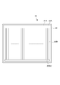
- FIG. 1 is a cross-sectional view showing a light control film according to the first embodiment of the present invention.
- This light control film 10 is formed by a film shape.
- the light control film 10 is a light control film that controls transmitted light using liquid crystal, and a liquid crystal material is formed by a lower laminate 13 and an upper laminate 12 that are first and second laminates in the form of a film, respectively.
- the liquid crystal cell 15 is produced by sandwiching the liquid crystal cell 15, and the liquid crystal cell 15 is produced by sandwiching the liquid crystal cell 15 by the linearly polarizing plates 16 and 17.
- the liquid crystal cell 15 is a transverse electric field type liquid crystal cell that drives the liquid crystal molecules 14A related to the liquid crystal layer 14 by the IPS / FFS method, and the linear polarizing plates 16 and 17 are arranged in a crossed Nicols arrangement.
- the transparent electrode 22A according to the FFS method is formed on the entire surface of the base 21A
- the transparent linear electrode 22B is formed with the insulating layer 23 interposed therebetween, and then the alignment layer 24A. Is provided.
- the alignment layer 24B is provided on the base material 21B.
- the first laminate is not limited to the lower laminate 13 and the second laminate is the upper laminate 12, but the first laminate constitutes the upper laminate 12, and the second laminate is The lower laminate 13 may be used.
- the light control film 10 is provided with a spacer 27 in the upper laminate 12 and / or the lower laminate 13 for keeping the thickness of the liquid crystal layer 14 constant.
- the spacer 27 may be provided on the upper laminate 12 or may be provided on both the upper laminate 12 and the lower laminate 13.
- the linear polarizing plates 16 and 17 are respectively provided with retardation films 18 and 19 for optical compensation on the liquid crystal cell 15 side.
- the retardation films 18 and 19 may be omitted as necessary.
- the light control film 10 controls the transmission of incident light by changing the orientation direction of the liquid crystal molecules 14A related to the liquid crystal layer 14 by changing the applied voltage between the electrodes 22A and 22B. And is configured to switch states.
- the light control film 10 is provided with a protective layer such as a hard coat layer on the surface opposite to the liquid crystal cell 15 of the linear polarizing plates 16 and 17.
- various transparent film materials having flexibility applicable to the liquid crystal cell 15 can be applied.
- the electrodes 22A and 22B can be widely applied in various configurations that are perceived as transparent.
- a transparent conductive layer made of ITO Indium Tin Oxide
- ITO Indium Tin Oxide
- the electrode 22A is produced.
- patterning is performed to produce the linear electrode 22B.
- various transparent insulating materials applicable to this type of liquid crystal cell can be applied, and various inorganic materials and organic materials can be applied.
- the alignment layers 24A and 24B various material layers applicable to the alignment layer such as polyimide are applied, and the surface of the material layer is formed by forming a fine line-shaped uneven shape by rubbing using a rubbing roll. .
- the alignment layer may be formed by forming a fine line-shaped uneven shape formed by the rubbing process by the shaping process, or by using the photo-alignment layer. Good.
- the alignment layers 24A and 24B are formed of a photo-alignment layer, as the photo-alignment material applicable to the photo-alignment layer, various materials to which the photo-alignment technique can be applied can be widely applied. Then, for example, a photodimerization type material is used.
- the photodimerization type material is described in “M. Schadt, K. Schmitt, V. Kozinkov and V. Chigrinov: Jpn. J. Appl. Phys., 31, 2155 (1992)”, “M. Schadt, H. Seiberle and A. Schuster: Nature, 381, 212 (1996).
- liquid crystal materials applied to this type of light control film can be widely applied to the liquid crystal layer 14, and for example, a liquid crystal material such as MLC 2166 manufactured by Merck Ltd. can be applied.
- the spacer 27 is made of a photoresist in this embodiment.
- a so-called bead spacer may be applied.
- a sealing agent 25 is arranged in a frame shape surrounding the liquid crystal layer 14.
- the sealing agent 25 prevents leakage of liquid crystal related to the liquid crystal layer 14, and furthermore, the upper laminate 12 and the lower laminate 13. Are held together.
- various materials capable of preventing the liquid crystal from leaking and holding the upper laminated body 12 and the lower laminated body 13 together can be applied.
- an epoxy resin is used.
- a thermosetting resin by an agent, an ultraviolet curable resin by an acrylic resin agent, a curable resin cured by heat and ultraviolet rays, or the like is applied.
- the linear polarizing plates 16 and 17 are so-called sheet polarizers, and after impregnating polyvinyl alcohol (PVA) with iodine or the like, an optical functional layer that performs an optical function as a polarizer is formed by stretching, and TAC ( The optical functional layer is sandwiched between base materials made of a transparent film material such as triacetyl cellulose).
- PVA polyvinyl alcohol
- TAC TAC
- FIG. 2 is a diagram showing the electrodes 22A and 22B in the lower laminate 13.
- the electrode 22A on the base 21A side is formed by forming a transparent conductive layer made of ITO on the entire surface of the base 21A, and power for driving is supplied through a power supply line (not shown).
- a power supply line (not shown).
- an insulating layer 23 is formed so as to cover the entire surface of the electrode 22A.
- the lower laminate 13 is provided with a power supply line 22BA to the linear electrode 22B at the end of the base 21A so as to extend along the long side of the base 21A, for example.
- the power supply line 22BA is formed of a metal material film having a small resistance value.
- the lower laminated body 13 is provided with linear electrodes 22B formed by patterning a transparent conductive layer with ITO at regular intervals so as to extend from the power supply line 22BA in a direction orthogonal to the power supply line 22BA. Driving power is supplied from the power supply line 22BA to the linear electrode 22B.
- the linear electrodes 22B are formed with a fine width of 10 ⁇ m or less and an interval of 10 ⁇ m or less.
- the liquid crystal material can be driven in all the portions where the electric field for driving is produced by the disconnected linear electrode 22B. As a result, a malfunctioning region occurs. Further, the resistance of the linear electrode 22B as viewed from the electron microscope supply end increases as the distance from the base portion of the power supply line 22BA increases, so that the voltage of the drive power supply decreases on the tip side. May occur.
- the light distribution of the liquid crystal material is controlled by the alternating electric field by applying an alternating power source in which the polarity of the driving power source is switched at regular time intervals to the electrodes 22 ⁇ / b> A and 22 ⁇ / b> B.
- the voltage of the driving power source is lowered on the tip side of the linear electrode 22B due to the resistance value of the linear electrode 22B, and luminance unevenness occurs.
- a power supply line may be provided similarly to the linear electrode 22B to supply driving power.
- the power supply lines of the linear electrodes 22B may be arranged along the long side on the other side, and more than three may be arranged at a constant pitch. Of course, it may be produced so as to extend along the short side.
- the resistance value can be reduced by shortening the length from the base portion of the power supply line 22BA to the tip side of the linear electrode 22B, thereby reducing the luminance value. Unevenness can be reduced. Further, it is possible to reduce the size of a malfunctioning area caused by disconnection.
- a bridge B that short-circuits the adjacent linear electrodes 22B is provided in the linear electrodes 22B.
- the drive power can be transmitted and received between the adjacent linear electrodes 22B by the bridge B, so that it is difficult to supply the drive power even if a disconnection occurs. Can be prevented from occurring, thereby effectively avoiding the occurrence of malfunctioning areas.
- the voltage of the driving power source in each part of the linear electrode 22B can be made uniform, thereby reducing the luminance unevenness.
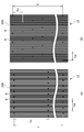
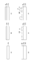
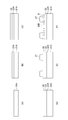
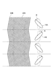
- FIG. 3A a pair of adjacent linear electrodes 22B is sequentially formed, and an odd-numbered pair and an even-numbered pair are each provided with a bridge B that short-circuits only the adjacent linear electrodes 22B.
- FIG. 6 is a diagram schematically showing a case in which an odd-numbered pair of bridges B and an even-numbered pair of bridges B are alternately provided in a direction in which the linear electrodes 22B extend at regular intervals. This is the case.
- the bridge B is provided so that the repeated pitch TH is 1 mm between the pair of adjacent linear electrodes 22B.
- the bridge B is manufactured with a width which is a length in the extending direction of the linear electrode 22 being 5 ⁇ m or more and 15 ⁇ m or less.
- FIG. 3 (B) is a diagram schematically showing the case where the bridge B for short-circuiting only the adjacent linear electrodes 22B is provided, and the repeated pitch in the continuous direction of the linear electrodes 22B.
- the TW is set to 1 mm, and the position where the bridge B is provided is sequentially shifted in the linear electrode extending direction in the extending direction of the linear electrode.
- the pitch TH of the arrangement of the bridges B in the extending direction of the linear electrodes 22B is 1 mm.
- the bridge B is provided almost uniformly on the entire surface of the light control film 10, so that it is possible to effectively avoid the occurrence of a malfunctioning region due to disconnection, and to further reduce luminance unevenness.
- the bridges B may be arranged regularly or irregularly.
- permeability falls locally because the horizontal electric field used for light control cannot be formed between lower electrode 22A.
- the bridge B is manufactured with a length in the extending direction of the linear electrode 22B of 5 ⁇ m or more and 15 ⁇ m or less as in this embodiment, such a portion where the transmittance is locally reduced is extremely limited. Thus, a reduction in transmittance due to the provision of the bridge B can be effectively avoided.
- the light control film there is no restriction on the area for controlling the transmitted light depending on the size of the pixel as in the liquid crystal display panel, and the transmitted light in a wide area is controlled.
- the higher the number of bridges B arranged at a higher density the more uniform the voltage of the drive power supply at each part of the linear electrode 22B can be reduced.
- the transmittance is reduced at the site of the bridge B, if the number is arranged too much, the transmittance is significantly reduced.
- interference fringes may occur. Therefore, the light control film has an interval of 10 mm to 100 mm that is at least several times the size of one pixel in the liquid crystal display panel in the extending direction of the linear electrodes between the linear electrodes (in FIG. In this case, the bridge B is repeatedly arranged, and this also effectively avoids a decrease in transmittance due to the provision of the bridge B, and further effectively avoids generation of interference fringes due to the bridge. Reduce unevenness.
- the bridge B may be produced so as to short-circuit only adjacent linear electrodes as in this embodiment, or may be produced so as to short-circuit three or more continuous linear electrodes, and short-circuited.
- the number of linear electrodes can be variously set.
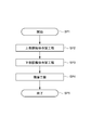
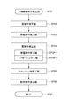
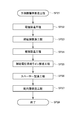
- FIG. 4 is a flowchart for explaining the manufacturing process of the light control film.
- the upper laminated body 12 and the lower laminated body 13 are produced in the upper laminated body producing process SP2 and the lower laminated body producing process SP3, respectively.
- the stacking step SP4 the upper stacked body 12 and the lower stacked body 13 are stacked with the liquid crystal layer 14 interposed therebetween, and then integrated with a sealant 25 to manufacture a liquid crystal cell.
- the liquid crystal cell thus prepared is laminated and integrated with the linear polarizing plate to prepare a light control film.
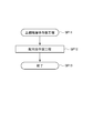
- FIG. 5 is a flowchart showing in detail the upper laminate manufacturing process SP2.
- the alignment layer manufacturing process SP12 applies the coating liquid related to the alignment layer 24B to the base material 21B, and then dries and cures the material to form the alignment layer 24B.
- a layer is formed.
- a fine line-shaped uneven shape is formed on the surface of the alignment layer material layer by a rubbing process using a rubbing roll, whereby the alignment layer 24B is manufactured, and thus the upper laminate 12 is manufactured.
- FIG. 6 is a flowchart showing in detail the lower laminate manufacturing process SP3.
- the lower laminate manufacturing step SP3 SP21
- the electrode manufacturing step SP22 in the electrode manufacturing step SP22, as shown in FIGS. 7A and 7B, a transparent electrode 22A made of ITO is formed on the entire surface of the base material 21A by sputtering. Is done.
- the insulating layer 23 is manufactured in the insulating layer manufacturing process SP23.
- the insulating layer 23 is manufactured by, for example, coating, drying, and curing of a coating liquid according to the material applied to the insulating layer 23.
- the linear electrode 22B is manufactured in the electrode manufacturing process SP24. More specifically, in this electrode manufacturing step SP24, as shown in FIG. 7D, in the conductive layer manufacturing step SP24-1, a linear electrode is formed on the entire surface of the substrate 21A by sputtering using a sputtering apparatus.
- the conductive layer 26 according to 22B is made of ITO.
- the patterning in the subsequent patterning step SP24-2 as shown in FIG. 7E, the linear electrode 22B and the bridge B are manufactured.
- the bridge B can be manufactured without increasing the number of processes by effectively using the process of manufacturing the linear electrode.
- the patterning step SP24-2 a photoresist is applied to the entire surface of the conductive layer and dried, followed by exposure processing and development processing.
- the conductive layer is patterned by setting the mask in this exposure process, and the linear electrode 22B and the bridge B are manufactured.
- this manufacturing process is performed in the spacer manufacturing process SP25 by applying a photoresist to the entire surface and drying it, and then exposing the spacer 27 by exposure processing and development processing using a mask. Make it.
- the spacer 27 is manufactured at the position where the bridge B is manufactured, thereby reducing the deterioration in transmittance due to the manufacturing of the bridge B.
- a material layer of the alignment layer 24A is formed by applying the coating liquid related to the alignment layer 24A, drying, and curing.
- a fine line-shaped uneven shape is formed on the surface of the alignment layer material layer by a rubbing process using a rubbing roll, and the alignment layer 24A is manufactured, whereby the lower laminate 13 is manufactured.
- this bridge by forming this bridge with a member of a linear electrode, and further by patterning at the time of manufacturing the linear electrode, the number of steps can be increased by effectively using the manufacturing process of the linear electrode. Bridges can be made without increasing.
- FIG. 8 is a flowchart showing the manufacturing process of the light control film according to the second embodiment of the present invention. This embodiment has the same configuration as that of the first embodiment except that the lower laminate manufacturing process shown in FIG. 8 is different.
- a bridge is produced using a spacer as a mask. That is, in the lower laminate manufacturing process SP31, in the electrode manufacturing process SP32, as shown in FIGS. 9A and 9B, the transparent electrode 22A made of ITO is manufactured on the entire surface of the base 21A by sputtering. Subsequently, in this manufacturing process, as shown in FIG. 9C, the insulating layer 23 is manufactured in the insulating layer manufacturing process SP33.
- the metal material related to the linear electrode 22B is deposited on the entire surface of the base 21A by sputtering using a sputtering apparatus as shown in FIG. 9D.
- the conductive layer 26 is produced.
- the linear electrode 22B is produced by patterning in the patterning process SP36. More specifically, after applying a photoresist, it is dried, and a portion corresponding to the linear electrodes or a portion corresponding to the space between the linear electrodes is selectively exposed using a mask. Then, after selectively removing the unexposed part or the exposed part of the photoresist, an etching process is performed, thereby producing the linear electrode 22B.
- the spacer 27 functions as a mask and the conductive layer 26 can be prevented from being removed by the etching process.
- the bridge B is also produced.
- the spacer 27 is formed with a diameter of 15 ⁇ m, so that the adjacent linear electrodes can be reliably short-circuited even when the masks related to the linear electrodes are displaced in any direction.
- the spacer 27 is manufactured with a diameter that is three times or more the width of the linear electrode, and the mask for the linear electrode is Even when displaced in the direction, the adjacent linear electrodes can be reliably short-circuited.
- the material layer of the alignment layer 24A is formed by applying the coating liquid related to the alignment layer 24A, drying, and curing.
- a fine line-shaped uneven shape is formed on the surface of the alignment layer material layer by a rubbing process using a rubbing roll, and the alignment layer 24A is manufactured, whereby the lower laminate 13 is manufactured.
- a spacer is produced, and then a linear electrode is produced by etching to produce a bridge using the spacer as a mask.
- the manufacturing process can be simplified.
- the transmittance is deteriorated between the bridge B portion and the spacer portion. This makes it possible to prevent the deterioration of the transmittance by producing a spacer at the site of the bridge B, but in this case, the alignment of the mask at the time of producing the spacer becomes complicated, and the alignment of the mask is shifted. The transmittance will decrease.
- FIG. 10 is a figure where it uses for description of the lower laminated body which concerns on the light control film which concerns on 3rd Embodiment of this invention. This embodiment is configured in the same way as the first embodiment or the second embodiment described above except that the lower laminate 33 according to FIG. 10 is applied.
- the lower laminated body 33 extends in the repeating direction of the linear electrode 22B, and is collected at a fixed portion in the extending direction of the linear electrode 22B so as to cross all the linear electrodes 22B in the repeating direction.
- a bridge B is produced, and thereby a linear electrode by the bridge B is produced.
- the linear electrode formed by the bridge B is formed in the extending direction of the linear electrode 22B with a constant interval of 10 mm to 100 mm or with an irregular interval, and is repeatedly provided with an electrode width of 5 ⁇ m to 15 ⁇ m. .
- the lower laminated body 33 is formed with an outer peripheral electrode 34 in a frame shape so as to surround from the outermost periphery, and driving power is supplied to the linear electrode 22B via the outer peripheral electrode 34.
- a linear electrode formed by the bridge B is formed so as to extend at both ends, and the linear electrode formed by the bridge B is directly connected to the outer peripheral electrode 34, whereby the driving electrode is directly connected to the electrode formed by the bridge B via the outer peripheral electrode 34. Power is supplied.
- the outer peripheral electrode is manufactured by applying a metal material such as copper or aluminum, which can have a resistance value smaller than that of ITO.
- the electrode by the bridge B may be manufactured at the same time as the peripheral electrode is manufactured by applying the metal material of the peripheral electrode.
- ITO may be applied to the outer peripheral electrode 34, and the outer peripheral electrode 34 may be formed simultaneously with the linear electrode 22B and the bridge B.
- the luminance unevenness can be further reliably reduced.
- the outer peripheral electrode 34 is made of a metal material having a small resistance value, it is difficult to make the outer peripheral electrode 34 on the base material and ensure a sufficient thickness.
- the light control film has a large area, the influence of the voltage drop at the outer peripheral electrode 34 cannot be ignored, and there is a risk of uneven brightness.
- each power supply system is indicated by an arrow.
- FIG. 12 is a figure where it uses for description of the lower laminated body which concerns on the light control film which concerns on 4th Embodiment of this invention. This embodiment is configured in the same way as the first to third embodiments described above except that the configuration according to FIG. 12 is different.
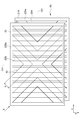
- the adjacent linear electrodes 22 are aligned in the extending direction of the linear electrode 22B, and are formed to meander in a triangular wave shape.
- a light control film is produced by multi-domain.
- the bridge B is arranged at the boundary between the domains related to the multi-domain.
- the transmittance is reduced, and the bridge B portion is also a portion where the transmittance is reduced.
- the bridge B is arranged at the domain boundary, the transmittance is reduced. An increase in the area can be prevented, and as a result, a decrease in the transmittance of the entire light control film can be prevented and luminance unevenness can be reduced.
- the present invention is not limited to this, and the present invention is widely applied to a case where a multi-domain is formed by bending the linear electrode. can do.
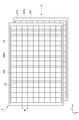
- FIG. 13 is a diagram showing the transparent electrode 22A and the linear electrode 22B of the lower laminate 13 together with the peripheral configuration.
- the light control film 10 (lower laminated body 13) of this embodiment is a rectangular shape by planar view.
- the transparent electrode 22A is formed on substantially the entire surface of the base material 21A of the lower laminate 13, and the voltage supply unit 22Aa is formed so as to extend along the long side and the short side of the base material 21A.
- the voltage supply unit 22Aa is formed in a frame shape on the outer peripheral portion of the base material 21A, and is formed of a material layer having a smaller sheet resistance value than the transparent electrode 22A.
- Transparent electrode 22A is laminated
- the voltage supply unit 22Aa is formed of a thin film or foil made of a metal material such as copper, silver, aluminum, nickel, or chromium, and is provided on the base 21A side or the liquid crystal layer 14 side of the transparent electrode 22A. Thereby, even if it is a case where the voltage for a drive is supplied from any site
- an AC voltage is supplied to one corner indicated by an arrow X.
- an insulating layer 23 is provided on the entire surface of the base 21 ⁇ / b> A including the transparent electrode 22 ⁇ / b> A and the voltage supply unit 22 ⁇ / b> Aa.
- a voltage supply unit 22Ba and a linear electrode 22B are provided on the insulating layer 23 .
- the transparent electrode 22A on which ITO is formed on the entire surface may be connected at several points via an FPC or the like as in the VA system. In the case of using metal wiring, it is better to form it simultaneously with the supply portion of ITO to the linear electrode 22B in order to reduce the number of process steps as will be described later.
- the voltage supply unit 22Ba is formed along the outer peripheral portion of the base member 21A with the same frame shape as the voltage supply unit 22Aa. From this voltage supply unit 22Ba, an AC voltage can be supplied to the linear electrode 22B.
- the voltage supply unit 22Ba has a rectangular frame shape with a long-side portion connected to the end of the linear electrode 22B and a short-side portion connecting both ends of the long-side portion. It is formed.
- the voltage supply unit 22Ba is a material layer having a sheet resistance smaller than that of the linear electrode 22B, for example, a thin film or foil made of a metal material such as silver, aluminum, nickel, or chromium.
- the linear electrodes 22B are repeatedly provided at a constant pitch. Further, the driving AC voltage is supplied from the corner indicated by the arrow X to the voltage supply unit 22Ba.
- voltage supply part 22Ba may be provided in the base-material 21A side with respect to the linear electrode 22B, and may be provided in the liquid-crystal layer 14 side.
- FIG. 14 is a diagram showing a detailed configuration of the linear electrode 22B.
- the linear electrode 22B is formed so that it may be bent, and it can also be multi-domained by this.
- the linear electrode 22B is formed so as to be inclined obliquely with respect to the extending direction of the linear electrode 22B, and the obliquely inclined direction is alternately switched at a constant pitch, thereby meandering in a triangular wave shape. Formed.
- the light control film 10 rotates the liquid crystal molecules 14A counterclockwise as indicated by an arrow A by driving the linear electrode 22B, or rotates the liquid crystal molecules 14A clockwise as indicated by an arrow B. Then, regions (domains) in which the behavior of liquid crystal molecules is different with respect to a change in electric field are alternately created. In the light control film 10, the appearances in the two domains having different rotation directions of the liquid crystal molecules 14A are averaged as described above, and the phenomenon of coloring due to the change in the viewing angle is alleviated.
- the direction of the inclination is switched at a constant pitch, and the pitch according to one period of the inclination switching is formed so as to change randomly in a continuous pair of domains related to this pitch.
- the light control film 10 is provided with a plurality of linear auxiliary voltage supply units 30 (see FIG. 13).
- the auxiliary voltage supply unit 30 equalizes the voltage at each part in the direction in which the linear electrode 22B extends, thereby achieving uniform transmission.
- the auxiliary voltage supply unit 30 has both ends connected to the short side of the voltage supply unit 22Ba.
- the auxiliary voltage supply unit 30 is linearly formed so as to extend along the long side of the base material 21A, and is repeatedly provided at a constant pitch P in the direction along the short side of the base material 21A. Accordingly, the auxiliary voltage supply unit 30 crosses the linear electrode 22B which is orthogonal to the linear electrode 22B and is continuous in each part in the extending direction of the linear electrode 22B. Further, since both ends of the auxiliary voltage supply unit 30 are connected to the voltage supply unit 22Ba, an AC voltage for driving is directly supplied to each part in the extending direction of the linear electrode 22B via the auxiliary voltage supply unit 30. Is done.
- the auxiliary voltage supply unit 30 is formed of a material layer having a smaller sheet resistance than the linear electrode 22B, for example, a thin film or foil made of a metal material such as silver, aluminum, nickel, or chromium. Therefore, the resistance value of the unit length is smaller than that of the linear electrode 22B.
- the resistance value of the unit length of the linear electrode 22B is about 2 ⁇ 10 5 ⁇ / cm to ⁇ 10 6 ⁇ / cm, and the resistance value of the unit length of the auxiliary voltage supply unit 30 is 2 ⁇ / cm to 100 ⁇ . / Cm or so.
- the auxiliary voltage supply unit 30 is repeatedly arranged with a pitch larger than the pitch of the linear electrodes 22B.
- the auxiliary voltage supply unit 30 by arranging the auxiliary voltage supply unit 30, the AC voltage is made uniform in each part of the linear electrode 22B, and the transmittance is made uniform. Further, when the voltage supply unit is made of a metal material, the resistance value can be reduced by setting the same cross-sectional area as compared with the case of using ITO. Thereby, the resistance value of the unit length can be made smaller than that of the linear electrode 22B. By arranging the auxiliary voltage supply unit 30, the AC voltage can be made uniform efficiently in each part of the linear electrode 22B.
- auxiliary voltage supply unit By providing the auxiliary voltage supply unit, it is possible to effectively avoid the occurrence of malfunctioning parts due to partial disconnection of the linear electrode 22B.
- the auxiliary voltage supply unit 30 may be provided on the base 21A side with respect to the linear electrode 22B, or may be provided on the liquid crystal layer 14 side.
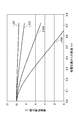
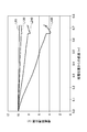
- FIG. 15 is a diagram showing a simulation result of the interelectrode potential difference between the transparent electrode 22A and the linear electrode 22B.
- the light control film 10 had a short side length of 80 cm and a long side length of 120 cm.
- the linear electrode 22B was made of ITO and had a thickness of 0.1 ⁇ m, a width of 6 ⁇ m, and a pitch of 12 ⁇ m.
- the transparent electrode 22A was made of ITO and had a thickness of 0.1 ⁇ m.
- the voltage supply unit 22Aa and the voltage supply unit 22Ba used copper thin films.
- the auxiliary voltage supply unit 30 uses a copper thin film and has a thickness of 0.3 ⁇ m, a width of 0.1 mm, and a pitch of 100 mm.
- reference numerals L60, L120, L240, and L480 are examples in the case where the light control film 10 is driven by a rectangular wave AC voltage having a frequency of 60 Hz, a frequency of 120 Hz, a frequency of 240 Hz, and a frequency of 480 Hz, respectively.
- FIG. 15 shows a potential difference between the transparent electrode 22 ⁇ / b> A and the linear electrode 22 ⁇ / b> B depending on the distance from the corner portion indicated by the symbol X as a feeding position.
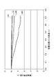
- FIG. 16 is a simulation result under the same conditions as FIG. 15 except that the pitch P of the auxiliary voltage supply unit 30 is 50 mm. Comparing FIG. 15 and FIG. 16, it can be seen that there is almost no difference in the potential difference between the electrodes even when the pitch P is changed from 100 mm to 50 mm.
- the pitch P is desirably 10 mm or more and 100 mm or less, and more desirably 20 mm or more and 50 mm or less.
- FIG. 17 is a simulation result under the same conditions as FIG. 14 except that the width of the auxiliary voltage supply unit 30 is changed from 0.1 mm to 0.2 mm.
- the width of the auxiliary voltage supply unit 30 is changed from 0.1 mm to 0.2 mm.
- the cross-sectional area of the auxiliary voltage supply unit 30 is doubled, and as a result, the change in the interelectrode potential difference is further reduced.
- the width is increased, the area occupied by the auxiliary voltage supply unit 30 is increased, so that a decrease in transmittance is predicted.
- the width is too narrow, the change in potential difference between the transparent electrode 22A and the linear electrode 22B in the extending direction of the linear electrode 22B cannot be sufficiently reduced, and it becomes difficult to make the transmittance uniform.
- the width of the auxiliary voltage supply unit 30 is desirably 5 ⁇ m or more and 0.1 mm or less, more preferably 10 ⁇ m or more and 50 ⁇ m or less, and more preferably 10 ⁇ m or more and 20 ⁇ m or less.
- the thickness of the auxiliary voltage supply unit 30 is desirably 0.1 ⁇ m or more and 1.0 ⁇ m or less, more preferably 0.2 ⁇ m or more and 0.5 ⁇ m or less, and more preferably 0.2 ⁇ m or more and 0.3 ⁇ m or less. It is desirable.
- FIG. 18 is a flowchart showing in detail the lower laminate manufacturing process SP3.
- FIG. 19 is a diagram showing in detail the lower laminate manufacturing process SP3.
- the transparent electrode 22A made of ITO is formed by sputtering on the entire surface of the base 21A (FIG. 19A) (FIG. 19B).
- ITO is preferably patterned from the entire surface. This is because when the linear electrode side is connected to the power source, if there is an ITO electrode on the lower surface, the possibility of short-circuiting increases.
- a metal thin film is produced by sputtering to produce the voltage supply unit 22Aa.
- the voltage supply unit 22Aa can be formed simultaneously with the voltage supply unit 22Ba and the voltage supply unit 22Ba.
- the insulating layer 23 is manufactured (FIG. 19C). It is desirable that the insulating layer 23 is also patterned. By exposing the transparent electrode 22A, which is a solid electrode of ITO, connection to a power source is facilitated, and the voltage supply unit 22Aa can be formed on the exposed ITO.
- the insulating layer 23 is manufactured by, for example, coating, drying, and curing of a coating liquid according to the material applied to the insulating layer 23.
- the linear electrode 22B is manufactured. More specifically, in this electrode manufacturing process SP24, after performing mask vapor deposition (FIG. 19D), the metal material related to the linear electrode 22B is formed on the entire surface of the base material 21A by sputtering using a sputtering apparatus. Is deposited to produce an ITO film. Subsequently, the linear electrode 22B is manufactured by patterning the ITO film (FIG. 19E).
- auxiliary voltage supply unit manufacturing step SP25 after forming the metal film related to the auxiliary voltage supply unit 30 and the voltage supply unit 22Ba (FIG. 19 (f)), patterning is performed (FIG. 19 (g)).
- the supply unit 30 and the voltage supply unit 22Ba are manufactured.
- the insulating layer 23 is patterned, a part of the surface of the metal electrode 22A made of solid ITO is exposed, a metal film is formed on the entire surface, and patterning can be performed simultaneously.
- the auxiliary electrode portion 22Ba can be formed simultaneously with the auxiliary electrode portion 22AA.
- the auxiliary voltage supply unit manufacturing process SP25 may be provided before the electrode manufacturing process SP24. Further, the auxiliary voltage supply unit 30 and the voltage supply unit 22Ba may be manufactured individually.
- a photoresist is applied on the entire surface and dried, and then the spacer 27 is manufactured by exposure processing and development processing using a mask.
- the alignment layer 24A is manufactured by applying the coating liquid related to the alignment layer 24A, drying, and exposing, whereby the lower laminate 13 is manufactured.
- the linear electrode 22B is arranged with the auxiliary voltage supply unit 30 having a smaller volume length resistance than the linear electrode 22B so as to extend across the continuous linear electrode 22B. did.
- permeability uniform can be provided regarding the light control film by an IPS / FFS system by supplying an alternating voltage also from the auxiliary voltage supply part 30.
- production of the malfunctioning location by the partial disconnection of the linear electrode 22B can be provided.
- the AC voltage can be made uniform and the transmittance can be made uniform in each part of the linear electrode 22B without impairing the transmittance.
- the transmittance can be made uniform with respect to the light control film by the IPS / FFS method with a simple configuration.
- An IPS / FFS method is provided by providing an auxiliary voltage supply unit manufacturing process that extends across the continuous linear electrode and provides an auxiliary voltage supply unit having a smaller unit length resistance value than the linear electrode.
- the light control film it is possible to provide a method for manufacturing a light control film capable of making the transmittance uniform. Furthermore, the manufacturing method of the light control film which can avoid effectively the generation
- An auxiliary voltage supply unit extending across the continuous linear electrode and having a smaller unit length resistance value than the linear electrode is disposed.
- FIG. 20 is a view showing a lower laminate 43 applied to the light control film according to the sixth embodiment of the present invention.
- a lower laminate 43 shown in FIG. 20 is applied instead of the lower laminate 13 described with reference to FIG.
- the lower laminate 43 is configured the same as the lower laminate 13 except that the auxiliary voltage supply unit 50 is different.
- the auxiliary voltage supply unit 50 is the same as the auxiliary voltage supply unit 30 except that the arrangement is different.
- the auxiliary voltage supply unit 50 is formed such that both sides of the symmetry axis are axisymmetric with respect to the center lines OH and OV that bisect the rectangular shape of the voltage supply unit 22Ba in the horizontal direction and the vertical direction, respectively. Thereby, it arrange
- the auxiliary voltage supply unit 50 is formed so as to have a line-symmetric shape so that the auxiliary voltage supply unit 50 intersects the linear electrode 22B at an angle of 45 degrees, for example, so as to obliquely cross the linear electrode 22B. Created.
- the direction in which the auxiliary voltage supply unit 50 extends is not limited to 45 degrees with respect to the linear electrode 22B.
- the auxiliary voltage supply unit 50 may extend in another direction extending away from the power supply position X when the power supply position X shown in FIG.
- the other direction is the power from one point to another point when considering one point near the power feeding position X and another point farther from the power feeding position X than the one point in the lower laminate 43.
- the supply route passes through the auxiliary voltage supply unit 50, the supply route extends in such a manner that the supply route is shortened as compared with a case where only the voltage supply unit 22Ba and the linear electrode 22B pass.
- auxiliary voltage supply part 50 is produced by the shape bent at an angle of 90 degrees in the center lines OH and OV.
- FIG. 21 is a simulation result of the light control film according to the sixth embodiment.
- the example of FIG. 21 is based on the same conditions as the example of FIG. 15 except that the auxiliary voltage supply unit 50 is created at an angle of 45 degrees.
- the transmittance can be made more uniform than in the first embodiment, as shown in FIG.
- the present invention is not limited to this, and can be widely applied to a case where a plurality of auxiliary voltage supply units are arranged so as to cross each other.
- the auxiliary voltage supply unit is formed linearly has been described.
- the present invention is not limited to this, and the auxiliary voltage supply unit may be formed using a curve.
- the present invention is not limited to this, and the pitch may be varied in each unit.
Landscapes
- Physics & Mathematics (AREA)
- Nonlinear Science (AREA)
- Chemical & Material Sciences (AREA)
- Crystallography & Structural Chemistry (AREA)
- General Physics & Mathematics (AREA)
- Optics & Photonics (AREA)
- Liquid Crystal (AREA)
- Mathematical Physics (AREA)
Abstract
FFS方式により調光フィルムを構成する場合に、線状電極の断線による動作不良の領域が発生を防止し、さらに輝度ムラを低減する。 第1及び第2の積層体13、12により液晶層14を挟持し、液晶層14に係る液晶分子14Aの配向を制御して透過光を制御する調光フィルム10において、第1の積層体13には、透明基材21Aの一方の面に、透明電極22A、絶縁層23、線状電極22Bが順次形成され、第1の積層体13の透明電極22A及び線状電極22B間の電界により液晶分子14Aの配向を制御し、隣接する線状電極22Bを短絡するブリッジが設けられる。
Description
本発明は、乗用車の窓等に貼り付けて外来光の透過を制御する調光フィルムに関する。
従来、例えば窓に貼り付けて外来光の透過を制御する調光フィルムに関する工夫が種々に提案されている(特許文献1、2)。このような調光フィルムの1つに、液晶を利用したものがある。この液晶を利用した調光フィルムは、透明電極を作製した透明フィルム材により液晶材料を挟持して液晶セルが作製され、この液晶セルを直線偏光板により挟持して作成される。これによりこの調光フィルムでは、液晶に印加する電界の可変により液晶の配向を可変して外来光を遮光したり透過したりし、さらには透過光量を可変したりし、これらにより外来光の透過を制御する。
この液晶セルの駆動には、液晶表示パネルについて提案されている種々の駆動方法を適用することができ、具体的には、例えばTN(Twisted Nematic)方式、IPS(In-Place-Switching)方式、VA(Virtical Alignment)方式等の駆動方式を適用することができる。
TN方式は、電界の印加により、液晶分子の配向を垂直方向と水平ねじれ方向とで変化させ、光の旋光性を利用して透過光量を制御する方式である。
また、IPS方式は、配向させた液晶分子を基板に対して横(水平)方向に回転させることにより透過光量を制御する方式である。
VA方式では、駆動電源の振幅が0Vの場合である無電界時、液晶層の液晶分子は垂直配向し、これにより調光フィルムは、入射光を遮光して遮光状態となる。また、この駆動電源の振幅を増大させて駆動電圧を立ち上げると、液晶層の液晶は水平配向し、調光フィルムは、入射光を透過させる。
また、IPS方式は、配向させた液晶分子を基板に対して横(水平)方向に回転させることにより透過光量を制御する方式である。
VA方式では、駆動電源の振幅が0Vの場合である無電界時、液晶層の液晶分子は垂直配向し、これにより調光フィルムは、入射光を遮光して遮光状態となる。また、この駆動電源の振幅を増大させて駆動電圧を立ち上げると、液晶層の液晶は水平配向し、調光フィルムは、入射光を透過させる。
しかしながら調光フィルムでは、例えば窓ガラスに貼り付けて種々の方向より見て取られる特長がある。これにより視野角依存性の少ないIPS方式により駆動することが好ましいと考えられる。
またこのIPS方式のうちの、FFS(フリンジフィールドスイッチング)方式(IPS/FFS方式)によれば、透過率を高くすることができ、これによりこの種の調光フィルムにおける液晶セルの駆動に適用して好ましいと考えられる。
ここでIPS/FFS方式では、液晶層を挟持する1対の基材のうちの一方の基材に駆動用の透明電極をまとめて作製する構成である。IPS/FFS方式では、この一方の基材の全面に、透明電極を作製した後、絶縁層を間に挟んで一定のピッチにより線状電極を作製し、この全面の透明電極と線状電極との間で発生する基材表面の面内方向の電界であるいわゆる横電界により液晶の配向を制御する。
ここでIPS/FFS方式では、液晶層を挟持する1対の基材のうちの一方の基材に駆動用の透明電極をまとめて作製する構成である。IPS/FFS方式では、この一方の基材の全面に、透明電極を作製した後、絶縁層を間に挟んで一定のピッチにより線状電極を作製し、この全面の透明電極と線状電極との間で発生する基材表面の面内方向の電界であるいわゆる横電界により液晶の配向を制御する。
ここでこのように全面の透明電極の上に絶縁層を間に挟んで線状電極を作製する場合、この線状電極の上では、液晶の配向に供する横電界が充分に発生しないことになる。従ってFFS方式において、線状電極の幅が大きくなると、この横電界が充分に発生しない領域が増大して透過率が低下することになる。これによりFFS方式において高い透過率を得るためには、電極幅10μm以下の微細幅により線状電極を作製することが必要である。
またFFS方式では、隣接する線状電極間の中央の部位でも、液晶の配向に供する横電界が充分に形成されないことになる。これによりFFS方式では、線状電極の間隔が広くなると、横電界が充分に発生しない領域が線状電極間で増大して透過率が低下することになる。これによりFFS方式で高い透過率を得るためには、線状電極の間隔も10μm以下とすることが必要になる。
ところでこのようにFFS方式により調光フィルムを作製する場合、電極幅10μm以下の微細幅の線状電極を10μm以下の間隔により大面積の調光を図る部位に配置することが必要になる。この場合、調光フィルムでは、この線状電極が局所的に断線すると、この断線した部位より先端側(電源より遠い側)では、駆動用の電源が供給されないことになる。これによりこのような部位では、液晶駆動用の電界を作製して調光することが困難になり、これにより動作不良の領域が発生する問題がある。特に、調光フィルムでは、大面積の領域で調光を図ることにより、断線により調光することができない動作不良領域も大面積により発生する問題がある。
またFFS方式による調光フィルムにおいて、電極幅10μm以下の微細幅の線状電極を10μm以下の間隔により大面積に配置する場合には、一方向に延長するように線状電極を並べて配置することになるものの、このようにすると線状電極の抵抗による電圧降下により各部で均一に電界を形成することが困難になり、その結果、調光フィルムに輝度ムラが発生する恐れもある。
また、このようなIPS/FFS方式による液晶表示パネルに関して、特許文献3には、線状電極を屈曲させてマルチドイン化し、一段と視野角特性を向上する構成が開示されている。
本発明はこのような状況に鑑みてなされたものであり、FFS方式により調光フィルムを構成する場合に、線状電極の断線による動作不良領域の発生を防止し、さらに輝度ムラを低減することを目的とする。
また、IPS/FFS方式による調光フィルムでは、基材の全面に形成された透明電極に、絶縁層を間に挟んで線状電極が一定ピッチにより並列に繰り返し配置されている。この全面の透明電極と線状電極との間で作成される面内方向の電界により液晶分子の配向が制御されて透過光が制御される。
調光フィルムは窓等に貼り付けて大面積により使用される。このように調光フィルムが大型化すると、線状電極の電圧は、給電点から離れるにつれ低下する。その結果、線状電極及び透明電極間の電位差が、線状電圧の長手方向における各部で変化し、これにより透過率が不均一化する。
本発明は、IPS/FFS方式による調光フィルムに関して、透過率を均一化することができる調光フィルムを提供することを目的とする。
また、IPS/FFS方式による調光フィルムでは、基材の全面に形成された透明電極に、絶縁層を間に挟んで線状電極が一定ピッチにより並列に繰り返し配置されている。この全面の透明電極と線状電極との間で作成される面内方向の電界により液晶分子の配向が制御されて透過光が制御される。
調光フィルムは窓等に貼り付けて大面積により使用される。このように調光フィルムが大型化すると、線状電極の電圧は、給電点から離れるにつれ低下する。その結果、線状電極及び透明電極間の電位差が、線状電圧の長手方向における各部で変化し、これにより透過率が不均一化する。
本発明は、IPS/FFS方式による調光フィルムに関して、透過率を均一化することができる調光フィルムを提供することを目的とする。
本発明者は、上記課題を解決するために鋭意研究を重ね、隣接する線状電極を短絡するブリッジを設ける、との着想に至り、本発明を完成するに至った。
具体的には、本発明では、以下のようなものを提供する。
(1)第1及び第2の積層体により液晶層を挟持し、前記液晶層に係る液晶分子の配向を制御して透過光を制御する調光フィルムにおいて、
前記第1の積層体には、透明基材の一方の面に、透明電極、絶縁層、線状電極が順次形成され、
前記第1の積層体の前記透明電極及び線状電極間の電界により前記液晶分子の配向を制御し、
隣接する前記線状電極を短絡するブリッジが設けられた調光フィルム。
前記第1の積層体には、透明基材の一方の面に、透明電極、絶縁層、線状電極が順次形成され、
前記第1の積層体の前記透明電極及び線状電極間の電界により前記液晶分子の配向を制御し、
隣接する前記線状電極を短絡するブリッジが設けられた調光フィルム。
(1)によれば、このブリッジにより隣接する線状電極間で駆動電源を相互に送受できることにより、線状電極が断線した場合にあっても、駆動用電源の供給が困難になる箇所の発生を防止することができ、これにより動作不良の領域の発生を有効に回避することができる。またブリッジを設けることにより線状電極の各部における駆動用電源の電圧も均一化することができ、これにより輝度ムラを低減することができる。
(2) (1)によれば、
前記ブリッジは、前記線状電極の部材により形成された調光フィルム。
前記ブリッジは、前記線状電極の部材により形成された調光フィルム。
(2)によれば、線状電極の作製工程を有効に利用して、何ら工程数を増大させることなくブリッジを作製することができる。
(3) (1)又は(2)において、
前記ブリッジが、10mm以上100mm以下の間隔により前記線状電極の延長方向に繰り返し設けられた調光フィルム。
前記ブリッジが、10mm以上100mm以下の間隔により前記線状電極の延長方向に繰り返し設けられた調光フィルム。
(3)によれば、ブリッジを設けたことによる透過率の低下を有効に回避し、さらにはブリッジによる干渉縞の発生等を有効に回避することができる。
(4) 透明フィルム材による基材に透明電極、絶縁層、線状電極、配向層を順次作製して第1の積層体を作製する第1の積層体作製工程と、
透明フィルム材による基材に配向層を作製して第2の積層体を作製する第2の積層体作製工程と、
液晶層を間に挟んで前記第1及び第2の積層体を積層して液晶セルを作製する積層工程とを備え、
前記第1の積層体作製工程は、
前記透明電極を作製する透明電極の作製工程と、
前記絶縁層を作製する絶縁層の作製工程と、
前記線状電極を作製する線状電極の作製工程とを備え、
前記線状電極の作製工程は、
前記絶縁層に導電層を作製する導電層作製工程と、
前記導電層をパターンニングして前記線状電極を作製するパターンニング工程を備え、
前記パターンニング工程におけるパターンニングにより、隣接する前記線状電極を短絡するブリッジを形成する調光フィルムの製造方法。
透明フィルム材による基材に配向層を作製して第2の積層体を作製する第2の積層体作製工程と、
液晶層を間に挟んで前記第1及び第2の積層体を積層して液晶セルを作製する積層工程とを備え、
前記第1の積層体作製工程は、
前記透明電極を作製する透明電極の作製工程と、
前記絶縁層を作製する絶縁層の作製工程と、
前記線状電極を作製する線状電極の作製工程とを備え、
前記線状電極の作製工程は、
前記絶縁層に導電層を作製する導電層作製工程と、
前記導電層をパターンニングして前記線状電極を作製するパターンニング工程を備え、
前記パターンニング工程におけるパターンニングにより、隣接する前記線状電極を短絡するブリッジを形成する調光フィルムの製造方法。
(4)によれば、このブリッジにより隣接する線状電極間で駆動電源を相互に送受できることにより、線状電極が断線した場合にあっても、駆動用電源の供給が困難になる箇所の発生を防止することができ、これにより動作不良の領域の発生を有効に回避することができる。またブリッジを設けることにより線状電極の各部における駆動用電源の電圧も均一化することができ、これにより輝度ムラを低減することができる。
(5) 透明フィルム材による基材に透明電極、絶縁層、線状電極、配向層を順次作製して第1の積層体を作製する第1の積層体作製工程と、
透明フィルム材による基材に配向層を作製して第2の積層体を作製する第2の積層体作製工程と、
液晶層を間に挟んで前記第1及び第2の積層体を積層して液晶セルを作製する積層工程とを備え、
前記第1の積層体作製工程は、
前記透明電極を作製する透明電極の作製工程と、
前記絶縁層を作製する絶縁層の作製工程と、
前記線状電極を作製する線状電極の作製工程とを備え、
前記線状電極の作製工程は、
前記絶縁層に導電層を作製する導電層作製工程と、
前記導電層に、前記液晶層の厚みを規制するスペーサーを作製するスペーサー作製工程と、
前記導電層をパターニングして、前記スペーサーによりマスクされる部位が隣接する前記線状電極を短絡するブリッジであるようにして、前記線状電極を作製するパターニング工程とを備える調光フィルムの製造方法。
透明フィルム材による基材に配向層を作製して第2の積層体を作製する第2の積層体作製工程と、
液晶層を間に挟んで前記第1及び第2の積層体を積層して液晶セルを作製する積層工程とを備え、
前記第1の積層体作製工程は、
前記透明電極を作製する透明電極の作製工程と、
前記絶縁層を作製する絶縁層の作製工程と、
前記線状電極を作製する線状電極の作製工程とを備え、
前記線状電極の作製工程は、
前記絶縁層に導電層を作製する導電層作製工程と、
前記導電層に、前記液晶層の厚みを規制するスペーサーを作製するスペーサー作製工程と、
前記導電層をパターニングして、前記スペーサーによりマスクされる部位が隣接する前記線状電極を短絡するブリッジであるようにして、前記線状電極を作製するパターニング工程とを備える調光フィルムの製造方法。
(5)によれば、このブリッジにより隣接する線状電極間で駆動電源を相互に送受できることにより、線状電極が断線した場合にあっても、駆動用電源の供給が困難になる箇所の発生を防止することができ、これにより動作不良の領域の発生を有効に回避することができる。またブリッジを設けることにより線状電極の各部における駆動用電源の電圧も均一化することができ、これにより輝度ムラを低減することができる。またスペーサーをマスクとして使用してブリッジを作製できることにより、透過率の低下を有効に回避して効率良く調光フィルムを作成することができる。
(6)透明電極上に絶縁層を介して複数の線状電極が配置された第1の積層体と、前記第1の積層体に対して対向して配置された第2の積層体と、前記第1の積層体及び前記第2の積層体により挟持され、前記透明電極と前記線状電極との間の電界により配向が制御される液晶分子を有する液晶層と、前記線状電極の端部同士を接続し、前記線状電極に交流電圧を供給する電圧供給部と、前記電圧供給部に接続され、前記複数の線状電極を横切って延び、前記線状電極に比べて単位長さの抵抗値が小さい複数の線状の補助電圧供給部と、を備える調光フィルム。
(7) (6)において、前記補助電圧供給部は、金属材料であることが好ましい。
(8) (6)又は(7)において、前記補助電圧供給部は、前記線状電極と直交していてもよい。
(9) (6)又は(7)において、前記補助電圧供給部が、前記線状電極を斜めに横切っていることが好ましい。
本発明によれば、FFS方式により調光フィルムを構成する場合に、線状電極の断線による動作不良領域の発生を防止し、さらに輝度ムラを低減することができる。
さらに、本発明によれば、IPS/FFS方式による調光フィルムに関して、透過率を均一化することができる調光フィルムを提供することができる。
さらに、本発明によれば、IPS/FFS方式による調光フィルムに関して、透過率を均一化することができる調光フィルムを提供することができる。
〔第1実施形態〕
図1は、本発明の第1実施形態に係る調光フィルムを示す断面図である。この調光フィルム10は、フィルム形状により形成される。この調光フィルム10は、液晶を利用して透過光を制御する調光フィルムであり、それぞれフィルム形状の第1及び第2の積層体である下側積層体13及び上側積層体12により液晶材料を挟持して液晶セル15が作製され、この液晶セル15を直線偏光板16、17により挟持して作成される。
ここで液晶セル15は、IPS/FFS方式により液晶層14に係る液晶分子14Aを駆動する横電界方式の液晶セルであり、直線偏光板16、17がクロスニコル配置により配置される。これにより下側積層体13は、基材21Aの全面に、FFS方式に係る透明電極22Aが形成され、絶縁層23を間に挟んで透明の線状電極22Bが形成され、続いて配向層24Aが設けられる。
また上側積層体12は、基材21Bに配向層24Bが設けられる。
なお、第1積層体が下側積層体13、第2積層体が上側積層体12である構成に限定されず、第1の積層体が上側積層体12を構成し、第2の積層体が下側積層体13であってもよい。
図1は、本発明の第1実施形態に係る調光フィルムを示す断面図である。この調光フィルム10は、フィルム形状により形成される。この調光フィルム10は、液晶を利用して透過光を制御する調光フィルムであり、それぞれフィルム形状の第1及び第2の積層体である下側積層体13及び上側積層体12により液晶材料を挟持して液晶セル15が作製され、この液晶セル15を直線偏光板16、17により挟持して作成される。
ここで液晶セル15は、IPS/FFS方式により液晶層14に係る液晶分子14Aを駆動する横電界方式の液晶セルであり、直線偏光板16、17がクロスニコル配置により配置される。これにより下側積層体13は、基材21Aの全面に、FFS方式に係る透明電極22Aが形成され、絶縁層23を間に挟んで透明の線状電極22Bが形成され、続いて配向層24Aが設けられる。
また上側積層体12は、基材21Bに配向層24Bが設けられる。
なお、第1積層体が下側積層体13、第2積層体が上側積層体12である構成に限定されず、第1の積層体が上側積層体12を構成し、第2の積層体が下側積層体13であってもよい。
調光フィルム10には、液晶層14の厚みを一定に保持するためのスペーサー27が上側積層体12及び又は下側積層体13に設けられる。ただし、スペーサー27は上側積層体12に設けられてもよく、上側積層体12及び下側積層体13の双方に設けられてもよい。
直線偏光板16、17は、それぞれ液晶セル15側に光学補償に供する位相差フィルム18、19が設けられる。なお位相差フィルム18、19は、必要に応じて省略してもよい。これによりこの調光フィルム10は、電極22A、22B間の印加電圧の可変により、液晶層14に係る液晶分子14Aの配向方向を可変して入射光の透過を制御し、例えば透過状態と遮光状態とで状態を切り替えるように構成される。なお調光フィルム10は、直線偏光板16及び又は17の液晶セル15とは逆側の面に、ハードコート層等による保護層が設けられる。
直線偏光板16、17は、それぞれ液晶セル15側に光学補償に供する位相差フィルム18、19が設けられる。なお位相差フィルム18、19は、必要に応じて省略してもよい。これによりこの調光フィルム10は、電極22A、22B間の印加電圧の可変により、液晶層14に係る液晶分子14Aの配向方向を可変して入射光の透過を制御し、例えば透過状態と遮光状態とで状態を切り替えるように構成される。なお調光フィルム10は、直線偏光板16及び又は17の液晶セル15とは逆側の面に、ハードコート層等による保護層が設けられる。
基材21A、21Bは、液晶セル15に適用可能な可撓性を有する各種の透明フィルム材を適用することができ、この実施形態では、両面にハードコート層が作製されてなるポリカーボネート等によるフィルム材が適用される。
電極22A、22Bは、透明と知覚される種々の構成を広く適用することができ、この実施形態では、透明電極材であるITO(Indium Tin Oxide)による透明導電層を基材21Aの全面に作製して電極22Aが作製される。また同様にして基材21Aの全面にITOによる透明導電層を作製した後、パターニングして線状電極22Bが作製される。
電極22A、22Bは、透明と知覚される種々の構成を広く適用することができ、この実施形態では、透明電極材であるITO(Indium Tin Oxide)による透明導電層を基材21Aの全面に作製して電極22Aが作製される。また同様にして基材21Aの全面にITOによる透明導電層を作製した後、パターニングして線状電極22Bが作製される。
絶縁層23は、この種の液晶セルに適用可能な各種の透明絶縁材料を適用することができ、各種の無機材料、有機材料を適用することができる。
配向層24A、24Bは、ポリイミド等の配向層に適用可能な各種材料層が適用され、この材料層の表面にラビングロールを使用したラビング処理により微細なライン状凹凸形状を作製して形成される。なおこのようなラビング処理による配向層に代えて、ラビング処理により作製した微細なライン状凹凸形状を賦型処理により作製して配向層を作製してもよく、また光配向層により作製してもよい。
配向層24A、24Bを、光配向層により形成する場合、光配向層に適用可能な光配向材料は、光配向の手法を適用可能な各種の材料を広く適用することができるが、本実施形態では、例えば光二量化型の材料を使用する。この光二量化型の材料については、「M.Schadt, K.Schmitt, V. Kozinkov and V. Chigrinov : Jpn. J. Appl.Phys., 31, 2155 (1992)」、「M. Schadt, H. Seiberle and A. Schuster : Nature, 381, 212(1996)」等に開示されている。
配向層24A、24Bを、光配向層により形成する場合、光配向層に適用可能な光配向材料は、光配向の手法を適用可能な各種の材料を広く適用することができるが、本実施形態では、例えば光二量化型の材料を使用する。この光二量化型の材料については、「M.Schadt, K.Schmitt, V. Kozinkov and V. Chigrinov : Jpn. J. Appl.Phys., 31, 2155 (1992)」、「M. Schadt, H. Seiberle and A. Schuster : Nature, 381, 212(1996)」等に開示されている。
液晶層14には、この種の調光フィルムに適用される各種の液晶材料を広く適用することができ、例えばメルク社製MLC2166等の液晶材料を適用することができる。
スペーサー27は、各種の樹脂材料を広く適用することができるものの、この実施形態ではフォトレジストにより作製される。なお、いわゆるビーズスペーサを適用してもよい。
なお液晶セル15は、液晶層14を囲む枠形状によりシール剤25が配置され、このシール剤25により液晶層14に係る液晶の漏出が防止され、さらには上側積層体12及び下側積層体13が一体に保持される。
ここでシール剤25は、液晶の漏出を防止すると共に、上側積層体12及び下側積層体13を一体に保持可能な種々の材料を適用することができるものの、この実施形態では、例えばエポキシ樹脂剤による熱硬化型樹脂やアクリル樹脂剤による紫外線硬化樹脂、熱及び紫外線で硬化する硬化樹脂等が適用される。
なお液晶セル15は、液晶層14を囲む枠形状によりシール剤25が配置され、このシール剤25により液晶層14に係る液晶の漏出が防止され、さらには上側積層体12及び下側積層体13が一体に保持される。
ここでシール剤25は、液晶の漏出を防止すると共に、上側積層体12及び下側積層体13を一体に保持可能な種々の材料を適用することができるものの、この実施形態では、例えばエポキシ樹脂剤による熱硬化型樹脂やアクリル樹脂剤による紫外線硬化樹脂、熱及び紫外線で硬化する硬化樹脂等が適用される。
直線偏光板16、17は、いわゆるシート・ポラライザーであり、ポリビニルアルコール(PVA)にヨウ素等を含浸させた後、延伸して偏光子としての光学的機能を果たす光学機能層が形成され、TAC(トリアセチルセルロース)等の透明フィルム材による基材により光学機能層を挟持して作製される。
〔線状電極の構成〕
図2は、下側積層体13における電極22A、22Bを示す図である。この実施形態において、基材21A側の電極22Aは、基材21Aの全面にITOによる透明導電層が作製されて形成され、図示しないで電源供給ラインにより駆動用の電源が供給される。さらに下側積層体13は、この電極22Aの全面を覆うように絶縁層23が形成される。下側積層体13は、例えば基材21Aの長辺に沿って延長するように、基材21Aの端部に線状電極22Bへの電源供給ライン22BAが形成される。ここで電源供給ライン22BAは、抵抗値の小さな金属材料膜等により形成される。下側積層体13は、この電源供給ライン22BAからこの電源供給ライン22BAと直交する方向に延長するように、ITOによる透明導電層のパターンニングによる線状電極22Bが一定の間隔により設けられ、この線状電極22Bに電源供給ライン22BAから駆動用電源が供給される。なお線状電極22Bは、電極幅10μm以下の微細幅により、10μm以下の間隔で配置して形成される。
図2は、下側積層体13における電極22A、22Bを示す図である。この実施形態において、基材21A側の電極22Aは、基材21Aの全面にITOによる透明導電層が作製されて形成され、図示しないで電源供給ラインにより駆動用の電源が供給される。さらに下側積層体13は、この電極22Aの全面を覆うように絶縁層23が形成される。下側積層体13は、例えば基材21Aの長辺に沿って延長するように、基材21Aの端部に線状電極22Bへの電源供給ライン22BAが形成される。ここで電源供給ライン22BAは、抵抗値の小さな金属材料膜等により形成される。下側積層体13は、この電源供給ライン22BAからこの電源供給ライン22BAと直交する方向に延長するように、ITOによる透明導電層のパターンニングによる線状電極22Bが一定の間隔により設けられ、この線状電極22Bに電源供給ライン22BAから駆動用電源が供給される。なお線状電極22Bは、電極幅10μm以下の微細幅により、10μm以下の間隔で配置して形成される。
これにより調光フィルム10では、線状電極22Bがこの電源供給ライン22BAの付け根で断線すると、この断線した線状電極22Bにより駆動用の電界が作製される部位の全てで、液晶材料を駆動できなくなり、動作不良の領域が発生することになる。また線状電極22Bは、電源供給ライン22BAの付け根部分にから遠ざかるに従って電顕供給端から見た抵抗値が増大することにより、駆動電源の電圧が先端側で低下し、その結果、輝度ムラが発生する恐れがある。なお調光フィルム10では、一定の時間間隔で駆動用電源の極性が切り替わる交番電源を電極22A、22Bに印加することにより、交番電界により液晶材料の配光を制御する。これにより線状電極22Bの抵抗値により線状電極22Bの先端側で駆動電源の電圧が低下し、輝度ムラが発生する。
なお基材21A側の電極22Aにあっても、線状電極22Bと同様に電源供給ラインを設けて駆動用電源を供給しても良い。また線状電極22Bの電源供給ラインは、電源供給ライン22BAに加えて、他方の側の長辺に沿って配置するようにしてもよく、さらには一定のピッチにより3本以上配置してもよく、また当然に短辺に沿って延長するように作製してもよい。このようにして電源供給ライン22BAの本数を増大させると、線状電極22Bに係る電源供給ライン22BAの付け根部分から先端側までの長さを短くして抵抗値を小さくすることができることにより、輝度ムラを低減することができる。また断線により発生する動作不良の領域の大きさを低減することができる。
さらにこの実施形態では、図3(A)及び(B)により示すように、隣接する線状電極22Bを短絡するブリッジBを、線状電極22Bに設ける。このようにブリッジBを設けた場合には、このブリッジBにより隣接する線状電極22B間で駆動電源を相互に送受できることにより、断線が発生した場合にあっても、駆動用電源の供給が困難になる箇所の発生を防止することができ、これにより動作不良の領域の発生を有効に回避することができる。またこのようにブリッジBを設けることにより線状電極22Bの各部における駆動用電源の電圧も均一化することができ、これにより輝度ムラを低減することができる。
ここで図3(A)は、隣接する線状電極22Bによる順次対を作製して、奇数番目の対と偶数番目の対とに、それぞれ隣接する線状電極22Bのみを短絡させるブリッジBを設ける場合を模式的に示す図であり、奇数番目の対に係るブリッジBと偶数番目の対に係るブリッジBとを、線状電極22Bの延長する方向に、一定の間隔を隔てて順次交互に設けた場合である。この図3(A)の例では、線状電極22Bの連続する方向には、ピッチTW=1mmによりブリッジBを設ける。また線状電極22Bの延長方向では、隣接する線状電極22Bの対で、繰り返しのピッチTHが1mmになるようにブリッジBを設ける。ここでブリッジBは、線状電極22の延長方向に係る長さである幅が5μm以上15μm以下により作製される。
これに対して図3(B)は、同様に隣接する線状電極22Bのみを短絡させるブリッジBを設ける場合を模式的に示す図であり、線状電極22Bの連続する方向への繰り返しのピッチTWを1mmとし、線状電極の延長方向で、ブリッジBを設ける箇所を線状電極の繰り返し方向に順次シフトさせたものである。なおこの図3(B)において、隣接する線状電極22Bの対に関して、この線状電極22Bの延長方向に係るブリッジBの配置のピッチTHは1mmである。
なおブリッジBは、調光フィルム10の全面にほぼ均一に設けるようにして、断線による動作不良の領域の発生を有効に回避することができ、さらには輝度ムラを低減することができる。またブリッジBは規則的に配置してもよく、不規則に配置してもよい。なおブリッジBを設けた箇所では、下層の電極22Aとの間で調光に供する横電界を形成できないことにより、局所的に透過率が低下することになる。しかしながらこの実施形態のように線状電極22Bの延長方向に係る長さが5μm以上15μm以下によりブリッジBを作製する場合には、このような局所的に透過率が低下する部位は、極めて限られた小面積の領域とすることができ、これによりブリッジBを設けたことによる透過率の低下を有効に回避することができる。
また調光フィルムでは、液晶表示パネルのような画素の大きさによる透過光を制御する領域の制限が無く、広い領域の透過光を制御することになる。これによりブリッジBを高密度に多数配置すればする程、線状電極22Bの各部における駆動用電源の電圧も均一化することができ、これにより輝度ムラを低減することができる。しかしながらブリッジBの部位で透過率が低下することにより、余りに多く配置すると、透過率の低下が著しくなる。また干渉縞が発生する恐れもある。そこで調光フィルムは、各線状電極間において、線状電極の延長方向に、少なくとも液晶表示パネルにおける1画素の大きさの数倍以上である10mm以上100mm以下の間隔(図3において、符号Tで示す間隔である)で繰り返しブリッジBが配置され、これによってもブリッジBを設けたことによる透過率の低下を有効に回避し、さらにはブリッジによる干渉縞の発生等を有効に回避して、輝度ムラを低減する。
またブリッジBは、この実施形態のように隣接する線状電極のみを短絡するように作製しても良く、連続する3本以上の線状電極を短絡させるように作製してもよく、短絡させる線状電極の本数にあっては種々に設定することができる。
〔製造工程〕
図4は、調光フィルムの製造工程の説明に供するフローチャートである。調光フィルムの製造工程は、上側積層体作製工程SP2及び下側積層体作製工程SP3において、それぞれ上側積層体12及び下側積層体13が作製される。また積層工程SP4において、液晶層14を間に挟んで、上側積層体12及び下側積層体13を積層した後、シール剤25により一体化して液晶セルが作製される。調光フィルムの製造工程は、このようにして作製した液晶セルを直線偏光板と積層一体化して調光フィルムが作製される。
図4は、調光フィルムの製造工程の説明に供するフローチャートである。調光フィルムの製造工程は、上側積層体作製工程SP2及び下側積層体作製工程SP3において、それぞれ上側積層体12及び下側積層体13が作製される。また積層工程SP4において、液晶層14を間に挟んで、上側積層体12及び下側積層体13を積層した後、シール剤25により一体化して液晶セルが作製される。調光フィルムの製造工程は、このようにして作製した液晶セルを直線偏光板と積層一体化して調光フィルムが作製される。
図5は、上側積層体作製工程SP2を詳細に示すフローチャートである。この上側積層体作製工程SP2(SP11)においては、配向層作製工程SP12において、基材21Bに配向層24Bに係る塗工液が塗工されて乾燥、硬化されることにより、配向層24Bの材料層が形成される。この製造工程は、ラビングロールを使用したラビング処理により、配向層材料層の表面に微細なライン状凹凸形状が作製されて配向層24Bが作製され、これにより上側積層体12が作製される。
図6は、下側積層体作製工程SP3を詳細に示すフローチャートである。この下側積層体作製工程SP3(SP21)においては、電極作製工程SP22において、図7(A)及び(B)に示すように、基材21Aの全面に、スパッタリングによりITOによる透明電極22Aが作製される。続いてこの製造工程は、絶縁層作製工程SP23において、図7(C)に示すように、絶縁層23が作製される。なおこの絶縁層作製工程は、絶縁層23に適用する材料に応じて例えば塗工液の塗工、乾燥、硬化により絶縁層23が作製される。
続いてこの製造工程は、電極作製工程SP24において、線状電極22Bが作製される。より具体的に、この電極作製工程SP24においては、導電層作製工程SP24-1において、図7(D)に示すように、スパッタリング装置を使用したスパッタリングにより、基材21Aの全面に、線状電極22Bに係る導電層26がITOにより作製される。また続くパターンニング工程SP24-2におけるパターンニングにより、図7(E)に示すように、線状電極22B及びブリッジBが作製される。これによりこの実施形態では、線状電極の作製工程を有効に利用して、何ら工程数を増大させることなくブリッジBを作製することができる。
すなわちパターンニング工程SP24-2においては、導電層の全面にフォトレジストを塗布して乾燥させた後、露光処理、現像処理する。パターンニング工程SP24-2は、この露光処理におけるマスクの設定により、図7(F)に示すように、導電層をパターンニングし、線状電極22B及びブリッジBを作製する。
このようにして線状電極22Bを作製すると、この製造工程は、スペーサー作製工程SP25において、全面にフォトレジストを塗工して乾燥させた後、マスクを使用した露光処理、現像処理によりスペーサー27を作製する。ここでこの実施形態では、ブリッジBの作製箇所にスペーサー27を作製するようにし、これによりブリッジBを作製したことによる透過率の劣化を低減する。
続いて配向層作製工程SP26において、配向層24Aに係る塗工液を塗工して乾燥、硬化することにより、配向層24Aの材料層が形成される。この製造工程は、ラビングロールを使用したラビング処理により、この配向層材料層の表面に微細なライン状凹凸形状が作製されて配向層24Aが作製され、これにより下側積層体13が作製される。
以上の構成によれば、隣接する線状電極を短絡するブリッジを設けることにより、このブリッジにより隣接する線状電極間で駆動電源を相互に送受でき、その結果、線状電極が断線した場合にあっても、駆動用電源の供給が困難になる箇所の発生を防止することができ、動作不良の領域の発生を有効に回避することができる。またブリッジを設けることにより線状電極の各部における駆動用電源の電圧も均一化することができ、これにより輝度ムラを低減することができる。
またこのブリッジを、線状電極の部材により形成することにより、さらには線状電極を作製する際のパターニングにより作製することにより、線状電極の作製工程を有効に利用して、何ら工程数を増大させることなくブリッジを作製することができる。
またさらにブリッジを、線状電極の延長方向に10mm以上100mm以下の間隔により繰り返し設けることにより、ブリッジを設けたことによる透過率の低下を有効に回避して充分に動作不良の領域の発生を回避し、輝度ムラを低減することができる。
〔第2実施形態〕
図8は、本発明の第2実施形態に係る調光フィルムの製造工程を示すフローチャートである。この実施形態では、この図8に示す下側積層体作製工程が異なる点を除いて、第1実施形態と同一に構成される。
図8は、本発明の第2実施形態に係る調光フィルムの製造工程を示すフローチャートである。この実施形態では、この図8に示す下側積層体作製工程が異なる点を除いて、第1実施形態と同一に構成される。
この下側積層体作製工程は、スペーサーをマスクとして使用してブリッジを作製する。すなわちこの下側積層体作製工程SP31においては、電極作製工程SP32において、図9(A)及び(B)に示すように、基材21Aの全面に、スパッタリングによりITOによる透明電極22Aを作製する。続いてこの製造工程は、絶縁層作製工程SP33において、図9(C)に示すように、絶縁層23を作製する。
続いてこの製造工程は、導電層作製工程SP34において、スパッタリング装置を使用したスパッタリングにより、図9(D)に示すように、基材21Aの全面に、線状電極22Bに係る金属材料を堆積して導電層26を作製する。
この製造工程は、続いてスペーサー作製工程SP35において、全面にフォトレジストを塗工して乾燥させた後、マスクを使用した露光処理、現像処理により、図9(E)に示すように、スペーサー27を作製する。
続いてこの製造工程は、パターンニング工程SP36におけるパターンニングにより、図9(F)に示すように、線状電極22Bを作製する。より具体的に、フォトレジストを塗工した後、乾燥させ、マスクを使用して線状電極に対応する部位、又は線状電極間に対応する部位を選択的に露光処理する。その後、フォトレジストの未露光の部位又は露光済みの部位を選択的に除去した後、エッチング処理し、これにより線状電極22Bを作製する。
このようにして線状電極を作製する場合、スペーサー27が作製されている部位にあっては、スペーサー27がマスクとして機能してエッチング処理によっては導電層26が除去されないようにすることができ、これによりこの実施形態では、ブリッジBを併せて作製する。なおこれによりスペーサー27は、直径が15μmにより形成され、これにより線状電極に係るマスクが何れの方向に変位して設けられた場合でも、確実に隣接する線状電極を短絡できるように構成される。なおこれによりスペーサー27は、線状電極の幅と線状電極の間隔とが等しい場合には、線状電極の幅の3倍以上の直径により作製して、線状電極に係るマスクが何れの方向に変位した場合でも、確実に隣接する線状電極を短絡することができる。
この製造工程は、続いて配向層作製工程SP37において、配向層24Aに係る塗工液を塗工して乾燥、硬化することにより、配向層24Aの材料層が形成される。この製造工程は、ラビングロールを使用したラビング処理により、この配向層材料層の表面に微細なライン状凹凸形状が作製されて配向層24Aが作製され、これにより下側積層体13が作製される。
この実施形態によれば、線状電極に係る導電層を作製した後、スペーサーを作製し、その後、エッチングして線状電極を作製することにより、スペーサーをマスクとして使用してブリッジを作製して製造工程を簡略化することができる。
すなわち第1実施形態により下側積層体を作製する場合、ブリッジBの部位とスペーサーの部位とで、透過率が劣化することになる。これによりブリッジBの部位にスペーサーを作製することにより、透過率の劣化を防止することができるものの、この場合、スペーサー作製時におけるマスクの位置合わせが煩雑になり、マスクの位置合わせがずれると、透過率が低下することになる。
しかしながらこの実施形態のように、スペーサーを事前に作製し、このスペーサーをエッチングのマスクとして使用してブリッジを作製すれば、スペーサー作製時におけるマスクの位置合わせを格段的に簡略化することができ、製造工程を簡略化することができる。
〔第3実施形態〕
図10は、本発明の第3実施形態に係る調光フィルムに係る下側積層体の説明に供する図である。この実施形態においては、この図10に係る下側積層体33が適用される点を除いて、上述の第1実施形態又は第2実施形態と同一に構成される。
図10は、本発明の第3実施形態に係る調光フィルムに係る下側積層体の説明に供する図である。この実施形態においては、この図10に係る下側積層体33が適用される点を除いて、上述の第1実施形態又は第2実施形態と同一に構成される。
ここでこの下側積層体33は、線状電極22Bの繰り返し方向に延長して、この繰り返し方向に係る全ての線状電極22Bを横切るように、線状電極22Bの延長方向の一定箇所に纏めてブリッジBが作製され、これによりブリッジBによる線状の電極が作製される。またこのブリッジBによる線状の電極は、線状電極22Bの延長方向に、10mm以上100mm以下の一定の間隔により、又は不規則な間隔により作製され、また電極幅5μm以上15μm以下により繰り返し設けられる。
またこの下側積層体33は、最外周より囲むように枠形状により外周電極34が作製され、この外周電極34を介して線状電極22Bに駆動用電源が供給される。さらにブリッジBによる線状の電極が両端で延長するよう形成されて外周電極34にブリッジBによる線状の電極が直接接続され、これによりブリッジBによる電極に直接、外周電極34を介して駆動用電源が供給される。ここで外周電極は、ITOによる場合に比して抵抗値を小さくすることが可能な、例えば銅、アルミニウム等の金属材料を適用して作製される。ブリッジBによる電極にあっては、この場合、この外周電極の金属材料を適用して、外周電極を作製する際に、同時に作製してもよい。また外周電極34にITOを適用して、外周電極34を線状電極22B、ブリッジBと同時に作製してもよい。
これによりこれによりこの実施形態では、一段と確実に輝度ムラを低減できるように構成される。
なお図10に示すように、抵抗値の小さい金属材料により外周電極34を作製する場合にあっても、基材に外周電極34を作製して厚みを充分に確保することが困難であることにより、調光フィルムが大面積になると、外周電極34における電圧降下の影響を無視し得ず、輝度ムラが発生する恐れがある。
そこで図10との対比により図11に示すように、複数個所より外周電極34に電源を供給するようにして、輝度ムラを低減することができる。なおこの図11では、各電源供給系統を矢印により示す。
〔第4実施形態〕
図12は、本発明の第4実施形態に係る調光フィルムに係る下側積層体の説明に供する図である。この実施形態においては、この図12に係る構成が異なる点を除いて、上述の第1実施形態~第3実施形態と同一に構成される。
図12は、本発明の第4実施形態に係る調光フィルムに係る下側積層体の説明に供する図である。この実施形態においては、この図12に係る構成が異なる点を除いて、上述の第1実施形態~第3実施形態と同一に構成される。
この実施形態においては、線状電極22Bの延長方向に、隣接する線状電極22が揃って、三角波形状により蛇行するように形成される。これにより電界の印加により、矢印Aにより示す反時計回りに液晶分子14Aが配向する部位と、これとは逆に、矢印Bにより示すように時計回りに液晶分子14Aが配向する部位とが形成され、マルチドメインにより調光フィルムが作製される。この実施形態では、このマルチドメインに係るドメインの境界にブリッジBが配置される。
このドメイン境界にあっては、透過率が低下する部位であり、ブリッジBの部位も透過率が低下する部位である、これによりドメイン境界にブリッジBを配置すれば、透過率の低下する部位の面積の増大を防止することができ、その結果、調光フィルム全体の透過率の低下を防止して輝度ムラを低減することができる。
〔他の実施形態〕
以上、本発明の実施に好適な具体的な構成を詳述したが、本発明は、本発明の趣旨を逸脱しない範囲で、上述の実施形態を組み合わせ、さらには上述の実施形態を種々に変更することができる。
以上、本発明の実施に好適な具体的な構成を詳述したが、本発明は、本発明の趣旨を逸脱しない範囲で、上述の実施形態を組み合わせ、さらには上述の実施形態を種々に変更することができる。
すなわち上述の実施形態では、線状電極を直線状に作製する場合について述べたが、本発明はこれに限らず、線状電極を屈曲させて作製することによりマルチドメイン化する場合にも広く適用することができる。
〔第5実施形態〕
第5実施形態の調光フィルム10の断面図は、電極の構成以外、第1実施形態の図1と同様である。同様な部分の説明は省略する。
第5実施形態の調光フィルム10の断面図は、電極の構成以外、第1実施形態の図1と同様である。同様な部分の説明は省略する。
〔電極の詳細〕
図13は、下側積層体13の透明電極22A、線状電極22Bを周辺構成と共に示す図である。本実施形態の調光フィルム10(下側積層体13)は、平面視で長方形形状である。下側積層体13の基材21Aの略全面に透明電極22Aが形成され、基材21Aの長辺及び短辺のそれぞれに沿って延びるように、電圧供給部22Aaが作成されている。
電圧供給部22Aaは、基材21Aの外周部において枠形状に、透明電極22Aに比べてシート抵抗値が小さな材料層により作成される。
図13は、下側積層体13の透明電極22A、線状電極22Bを周辺構成と共に示す図である。本実施形態の調光フィルム10(下側積層体13)は、平面視で長方形形状である。下側積層体13の基材21Aの略全面に透明電極22Aが形成され、基材21Aの長辺及び短辺のそれぞれに沿って延びるように、電圧供給部22Aaが作成されている。
電圧供給部22Aaは、基材21Aの外周部において枠形状に、透明電極22Aに比べてシート抵抗値が小さな材料層により作成される。
透明電極22Aは、外周部において電圧供給部22Aaに積層され、電圧供給部22Aaを介して駆動用の交流電圧が供給される。
電圧供給部22Aaは、銅、銀、アルミニウム、ニッケル、クロム等による金属材料による薄膜、箔により形成され、透明電極22Aの基材21A側又は液晶層14側に設けられる。
これにより調光フィルム10は、電圧供給部22Aaの何れの部位より駆動用の電圧を供給する場合であっても、少なくとも外周部では、透明電極22Aに均一な電圧が印加されるように構成される。なお、図13においては、矢印Xにより示す1つの角部に交流電圧が供給される。
電圧供給部22Aaは、銅、銀、アルミニウム、ニッケル、クロム等による金属材料による薄膜、箔により形成され、透明電極22Aの基材21A側又は液晶層14側に設けられる。
これにより調光フィルム10は、電圧供給部22Aaの何れの部位より駆動用の電圧を供給する場合であっても、少なくとも外周部では、透明電極22Aに均一な電圧が印加されるように構成される。なお、図13においては、矢印Xにより示す1つの角部に交流電圧が供給される。
下側積層体13において、透明電極22A、電圧供給部22Aaを備えた基材21Aの全面に絶縁層23が設けられている。絶縁層23上には、電圧供給部22Ba、線状電極22Bが設けられる。
なお、ITOが全面に作製された透明電極22Aに関しては、VA方式と同様に、FPCなどを介して、何点か接続しても良い。金属配線を用いる場合には、後述するようにプロセスのステップ数を減らすため、ITOの線状電極22Bへの供給部と同時に形成した方が良い。
ここで電圧供給部22Baは、電圧供給部22Aaと同様の枠形状により基材21Aの外周部に沿って形成される。この電圧供給部22Baより、線状電極22Bに交流電圧が供給可能である。
なお、ITOが全面に作製された透明電極22Aに関しては、VA方式と同様に、FPCなどを介して、何点か接続しても良い。金属配線を用いる場合には、後述するようにプロセスのステップ数を減らすため、ITOの線状電極22Bへの供給部と同時に形成した方が良い。
ここで電圧供給部22Baは、電圧供給部22Aaと同様の枠形状により基材21Aの外周部に沿って形成される。この電圧供給部22Baより、線状電極22Bに交流電圧が供給可能である。
電圧供給部22Baは、線状電極22Bの端部と接続された長辺側の部位と、この長辺側の部位の両端部を接続する短辺側の部位とにより、長方形形状の枠形状により形成される。電圧供給部22Baは、線状電極22Bに比べてシート抵抗の小さな材料層である、例えば、銀、アルミニウム、ニッケル、クロム等による金属材料による薄膜、箔により形成される。
線状電極22Bは、一定のピッチにより繰り返し設けられている。また、矢印Xにより示す角部より電圧供給部22Baに駆動用の交流電圧が供給される。なお、電圧供給部22Baは、線状電極22Bに対して基材21A側に設けてもよく、液晶層14側に設けてもよい。
図14は、線状電極22Bの詳細構成を示す図である。調光フィルム10では、線状電極22Bが屈曲するように形成され、これによりマルチドメイン化することもできる。
すなわち線状電極22Bは、線状電極22Bの延びる方向に対して斜めに傾くようにして、この斜めに傾く方向が一定のピッチで交互に切り替わるように形成され、これにより三角波形状により蛇行するように形成される。
調光フィルム10は、線状電極22Bの駆動により、矢印Aにより示すように、液晶分子14Aを反時計方向に回転させたり、矢印Bにより示すように、液晶分子14Aを時計方向に回転させたりし、電界の変化に対して液晶分子の挙動の異なる領域(ドメイン)を交互に作成する。
調光フィルム10では、このように液晶分子14Aの回転方向が異なる2つのドメインにおける見え方が平均値化され、視野角の変化による色付きの現象が緩和される。
調光フィルム10は、線状電極22Bの駆動により、矢印Aにより示すように、液晶分子14Aを反時計方向に回転させたり、矢印Bにより示すように、液晶分子14Aを時計方向に回転させたりし、電界の変化に対して液晶分子の挙動の異なる領域(ドメイン)を交互に作成する。
調光フィルム10では、このように液晶分子14Aの回転方向が異なる2つのドメインにおける見え方が平均値化され、視野角の変化による色付きの現象が緩和される。
このように一定のピッチで傾きの向きを切り替えるようにして、傾きの切り替わりの1周期に係るピッチが、このピッチに係る1対のドメインの連続でランダムに変化するように形成される。
これにより調光フィルム10ではマルチドメインの作製に係る線状電極の蛇行に係る規則性が緩和され、風景等が2重像により見て取られる現象を有効に回避する。
これにより調光フィルム10ではマルチドメインの作製に係る線状電極の蛇行に係る規則性が緩和され、風景等が2重像により見て取られる現象を有効に回避する。
調光フィルム10には、複数の線状の補助電圧供給部30が設けられている(図13参照)。補助電圧供給部30により、線状電極22Bの延びる方向の各部における電圧が均一化され、透過率の均一化が図られる。
補助電圧供給部30は、電圧供給部22Baの短辺側に両端が接続されている。補助電圧供給部30は、基材21Aの長辺に沿って延びるように直線状に形成され、基材21Aの短辺に沿った方向に一定のピッチPで繰り返して設けられる。
これにより線状電極22Bの延びる方向の各部で、線状電極22Bと直交し、連続する線状電極22Bを補助電圧供給部30が横切る。
また、補助電圧供給部30の両端が電圧供給部22Baに接続されているので、補助電圧供給部30を介して、線状電極22Bの延びる方向の各部に、直接、駆動用の交流電圧が供給される。
これにより線状電極22Bの延びる方向の各部で、線状電極22Bと直交し、連続する線状電極22Bを補助電圧供給部30が横切る。
また、補助電圧供給部30の両端が電圧供給部22Baに接続されているので、補助電圧供給部30を介して、線状電極22Bの延びる方向の各部に、直接、駆動用の交流電圧が供給される。
補助電圧供給部30は、線状電極22Bに比べてシート抵抗値の小さな材料層により、例えば、銀、アルミニウム、ニッケル、クロム等による金属材料による薄膜、箔により形成されている。したがって線状電極22Bに比べて単位長さの抵抗値が小さい。
例えば、線状電極22Bの単位長さの抵抗値は、2×10⁵Ω/cm~×106Ω/cm程度で、補助電圧供給部30の単位長さの抵抗値は2Ω/cm~100Ω/cm程度である。
補助電圧供給部30は、線状電極22Bのピッチに比べて大きなピッチにより繰り返し配置される。
例えば、線状電極22Bの単位長さの抵抗値は、2×10⁵Ω/cm~×106Ω/cm程度で、補助電圧供給部30の単位長さの抵抗値は2Ω/cm~100Ω/cm程度である。
補助電圧供給部30は、線状電極22Bのピッチに比べて大きなピッチにより繰り返し配置される。
本実施形態によると、補助電圧供給部30を配置したことによって、線状電極22Bの各部で交流電圧が均一化され、透過率が均一化される。
また、金属材料により電圧供給部を作成する場合、ITOを使用する場合に比べて、断面積を同一に設定して抵抗値を減少することができる。これにより線状電極22Bに比べて単位長さの抵抗値を小さくすることができる。補助電圧供給部30を配置したことによって、線状電極22Bの各部で効率よく交流電圧を均一化することができる。
また、金属材料により電圧供給部を作成する場合、ITOを使用する場合に比べて、断面積を同一に設定して抵抗値を減少することができる。これにより線状電極22Bに比べて単位長さの抵抗値を小さくすることができる。補助電圧供給部30を配置したことによって、線状電極22Bの各部で効率よく交流電圧を均一化することができる。
補助電圧供給部を設けることにより、線状電極22Bの部分的な断線による動作不良個所の発生を有効に回避することができる。
補助電圧供給部30は、線状電極22Bに対して基材21A側に設けてもよく、液晶層14側に設けてもよい。
〔シミュレーション結果〕
図15は、透明電極22A、線状電極22B間における電極間電位差のシミュレーション結果を示す図である。
調光フィルム10は、短辺の長さ80cm、長辺の長さを120cmとした。
線状電極22Bは、ITOを用い、厚み0.1μm、幅6μm、ピッチ12μmとした。
透明電極22Aは、ITOを用い、厚み0.1μmとした。
電圧供給部22Aa、電圧供給部22Baは、銅薄膜を用いた。
補助電圧供給部30は、銅薄膜を用い、厚み0.3μm、幅0.1mm、ピッチ100mmとした。
図15は、透明電極22A、線状電極22B間における電極間電位差のシミュレーション結果を示す図である。
調光フィルム10は、短辺の長さ80cm、長辺の長さを120cmとした。
線状電極22Bは、ITOを用い、厚み0.1μm、幅6μm、ピッチ12μmとした。
透明電極22Aは、ITOを用い、厚み0.1μmとした。
電圧供給部22Aa、電圧供給部22Baは、銅薄膜を用いた。
補助電圧供給部30は、銅薄膜を用い、厚み0.3μm、幅0.1mm、ピッチ100mmとした。
図中、符号L60、L120、L240、L480は、それぞれ周波数60Hz、周波数120Hz、周波数240Hz、周波数480Hzによる矩形波の交流電圧により調光フィルム10を駆動した場合の例である。
図15では、符号Xにより示した角部を給電位置として、この角部からの距離による、透明電極22Aと線状電極22Bとの間の電位差を示す。
図15では、符号Xにより示した角部を給電位置として、この角部からの距離による、透明電極22Aと線状電極22Bとの間の電位差を示す。
図16は、補助電圧供給部30のピッチPを50mmとした点を除いて、図15と同一の条件によるシミュレーション結果である。図15と図16とを比較すると、ピッチPを100mmから50mmにしても、電極間電位差には殆ど差はないことが分かる。
ピッチPを細かくすると、補助電圧供給部30の占める面積が増大することによる透過率の低下が予測される。しかし、ピッチPが大きすぎると、線状電極22Bの延びる方向における透明電極22Aと線状電極22Bとの間の電位差の変化を低減できなくなり、透過率を均一化することが困難になる。
これによりピッチPは、10mm以上100mm以下であることが望ましく、さらに好ましくは20mm以上50mm以下であることが望ましい。
これによりピッチPは、10mm以上100mm以下であることが望ましく、さらに好ましくは20mm以上50mm以下であることが望ましい。
図17は、補助電圧供給部30の幅を0.1mmから0.2mmとした点を除いて、図14と同一の条件によるシミュレーション結果である。図17によれば、補助電圧供給部30の幅を2倍にしたことにより、補助電圧供給部30の断面積が2倍となり、その結果、電極間電位差における変化が一段と低減していることが分かる。
ここで幅を広くすると、補助電圧供給部30の占める面積が増大することにより透過率の低下が予測される。しかしながら幅が狭すぎると、線状電極22Bの延びる方向における透明電極22Aと線状電極22Bとの間の電位差の変化を十分に低減できなくなり、透過率を均一化することが困難になる。
これにより補助電圧供給部30の幅は、5μm以上0.1mm以下であることが望ましく、さらに好ましくは10μm以上50μm以下、より好ましくは10μm以上20μm以下であることが望ましい。
ここで幅を広くすると、補助電圧供給部30の占める面積が増大することにより透過率の低下が予測される。しかしながら幅が狭すぎると、線状電極22Bの延びる方向における透明電極22Aと線状電極22Bとの間の電位差の変化を十分に低減できなくなり、透過率を均一化することが困難になる。
これにより補助電圧供給部30の幅は、5μm以上0.1mm以下であることが望ましく、さらに好ましくは10μm以上50μm以下、より好ましくは10μm以上20μm以下であることが望ましい。
また補助電圧供給部30は、厚みを厚くすると液晶層の厚み(セルギャップ)に影響を与える。しかしながら厚みが薄すぎると、線状電極22Bの延びる方向における透明電極22Aと線状電極22Bとの間の電位差の変化を十分に低減できなくなり、透過率を均一化することが困難になる。
これにより補助電圧供給部30の厚みは、0.1μm以上1.0μm以下であることが望ましく、さらに好ましくは0.2μm以上0.5μm以下、より好ましくは0.2μm以上0.3μm以下であることが望ましい。
これにより補助電圧供給部30の厚みは、0.1μm以上1.0μm以下であることが望ましく、さらに好ましくは0.2μm以上0.5μm以下、より好ましくは0.2μm以上0.3μm以下であることが望ましい。
〔製造工程〕
調光フィルムの製造工程は、図18に示す下側積層体作製工程SP3以外、第1実施形態の図4及び図5と同様である。同様な部分の説明は省略する。
調光フィルムの製造工程は、図18に示す下側積層体作製工程SP3以外、第1実施形態の図4及び図5と同様である。同様な部分の説明は省略する。
図18は、下側積層体製造工程SP3を詳細に示すフローチャートである。図19は、下側積層体製造工程SP3を詳細に示す図である。下側積層体製造工程SP3(SP21)においては、電極製造工程SP22で、基材21Aの全面(図19(a))に、スパッタリングによりITOによる透明電極22Aが作製される(図19(b))。ITOは全面よりパターニングされている方が好ましい。線状電極側を電源に接続するとき、下面にITO電極があるとショートする可能性が高くなるためである。
また透明電極22Aの作成の前に、又は後に、スパッタリングにより金属薄膜を作成して電圧供給部22Aaが作成される。なお、電圧供給部22Aaは、電圧供給部22Ba電圧供給部22Baと同時に形成する事も可能である。
また透明電極22Aの作成の前に、又は後に、スパッタリングにより金属薄膜を作成して電圧供給部22Aaが作成される。なお、電圧供給部22Aaは、電圧供給部22Ba電圧供給部22Baと同時に形成する事も可能である。
続いて絶縁層製造工程SP23において、絶縁層23が製造される(図19(c))。なお、絶縁層23もパターニングされていた方が望ましい。ITOのベタ電極である透明電極22Aを露出させる事で、電源との接続が容易になり、露出したITO上に電圧供給部22Aaを形成することが出来る。
なおこの絶縁層製造工程は、絶縁層23に適用する材料に応じて例えば塗工液の塗工、乾燥、硬化により絶縁層23が製造される。
なおこの絶縁層製造工程は、絶縁層23に適用する材料に応じて例えば塗工液の塗工、乾燥、硬化により絶縁層23が製造される。
続いて、電極製造工程SP24において、線状電極22Bが製造される。より具体的に、この電極製造工程SP24においては、マスク蒸着を行った後(図19(d))、スパッタリング装置を使用したスパッタリングにより、基材21Aの全面に、線状電極22Bに係る金属材料を堆積してITO膜を製造する。また続いてこのITO膜のパターンニングにより、線状電極22Bを製造する(図19(e))。
続く補助電圧供給部製造工程SP25において、補助電圧供給部30、電圧供給部22Baに係る金属膜を作成した後(図19(f))、パターニングし(図19(g))、これにより補助電圧供給部30、電圧供給部22Baを製造する。
絶縁層23をパターニングした場合、ベタITOである金属電極22Aの面を一部露出させ、全面に金属膜を製膜して、同時にパターニングする事ができる。これにより、補助電極部22Baは補助電極部22AAと同時に形成することができる。
なお補助電圧供給部製造工程SP25は、電極製造工程SP24の前に設けるようにしてもよい。また補助電圧供給部30、電圧供給部22Baを個別に製造してもよい。
絶縁層23をパターニングした場合、ベタITOである金属電極22Aの面を一部露出させ、全面に金属膜を製膜して、同時にパターニングする事ができる。これにより、補助電極部22Baは補助電極部22AAと同時に形成することができる。
なお補助電圧供給部製造工程SP25は、電極製造工程SP24の前に設けるようにしてもよい。また補助電圧供給部30、電圧供給部22Baを個別に製造してもよい。
スペーサー製造工程SP26において、全面にフォトレジストを塗工して乾燥させた後、マスクを使用した露光処理、現像処理によりスペーサー27を製造する。
配向層製造工程SP27において、配向層24Aに係る塗工液を塗工して乾燥、露光することにより、配向層24Aを製造し、これにより下側積層体13が製造される。
(1)本実施形態によれば、連続する線状電極22Bを横切って延びるように、線状電極22Bに比べて体積長さの抵抗値の小さな補助電圧供給部30を線状電極22Bを配置した。
そして、補助電圧供給部30からも交流電圧を供給することにより、IPS/FFS方式による調光フィルムに関して、透過率を均一化することができる調光フィルムを提供することができる。
さらに線状電極22Bの部分的な断線による動作不良個所の発生を有効に回避することができる調光フィルムを提供することができる。
そして、補助電圧供給部30からも交流電圧を供給することにより、IPS/FFS方式による調光フィルムに関して、透過率を均一化することができる調光フィルムを提供することができる。
さらに線状電極22Bの部分的な断線による動作不良個所の発生を有効に回避することができる調光フィルムを提供することができる。
(2)補助電圧供給部30を金属材料により作製することにより、透過率を損なわないようにして、線状電極22Bの各部で効率よく交流電圧を均一化し、透過率を均一化することができる。
(3)水平方向及び垂直方向に線対称に補助電圧供給部を配置することにより、透過率の不均一さが目立たないようにすることができる。
(4)補助電圧供給部30が、線状電極22Bと直交するように作成されていることにより、簡易な構成によりIPS/FFS方式による調光フィルムに関して、透過率を均一化することができる。
(5)連続する前記線状電極を横切って延び、線状電極に比べて単位長さの抵抗値の小さな補助電圧供給部を設ける補助電圧供給部製造工程を備えることにより、IPS/FFS方式による調光フィルムに関して、透過率を均一化することができる調光フィルムの製造方法を提供することができる。
さらに線状電極22Bの部分的な断線による動作不良個所の発生を有効に回避することができる調光フィルムの製造方法を提供することができる。
さらに線状電極22Bの部分的な断線による動作不良個所の発生を有効に回避することができる調光フィルムの製造方法を提供することができる。
(6)連続する線状電極を横切って延び、線状電極に比べて単位長さの抵抗値の小さな補助電圧供給部を配置した。
電圧供給部により線状電極に交流電圧を供給することにより、IPS/FFS方式による調光フィルムに関して、透過率を均一化することができる調光フィルムの駆動方法を提供することができる。
さらに線状電極22Bの部分的な断線による動作不良個所の発生を有効に回避することができる調光フィルムの駆動方法を提供することができる。
電圧供給部により線状電極に交流電圧を供給することにより、IPS/FFS方式による調光フィルムに関して、透過率を均一化することができる調光フィルムの駆動方法を提供することができる。
さらに線状電極22Bの部分的な断線による動作不良個所の発生を有効に回避することができる調光フィルムの駆動方法を提供することができる。
〔第6実施形態〕
図20は、本発明の第6実施形態に係る調光フィルムに適用される下側積層体43を示す図である。本実施形態では、図13について説明した下側積層体13に代えてこの図20に示す下側積層体43が適用される。
図20は、本発明の第6実施形態に係る調光フィルムに適用される下側積層体43を示す図である。本実施形態では、図13について説明した下側積層体13に代えてこの図20に示す下側積層体43が適用される。
下側積層体43は、補助電圧供給部50が異なる点を除いて、下側積層体13と同一に構成される。また補助電圧供給部50は、配置が異なる点を除いて補助電圧供給部30と同一である。
補助電圧供給部50は、電圧供給部22Baに係る長方形形状を水平方向及び垂直方向に2等分する中心線OH及びOVをそれぞれ対称軸にして、この対称軸の両側が線対称により形成され、これにより透過率の不均一さが目立たないように配置される。
このように線対称形状により作製するようにして、補助電圧供給部50は、線状電極22Bを斜めに横切るように、例えば、線状電極22Bと45度の角度を成して交差するように作成される。
なお、補助電圧供給部50の延びる方向は、この線状電極22Bに対する45度に限定されない。補助電圧供給部50は、図20に示す給電位置Xを基準としたときに、この給電位置Xから離れる方向に延びる他の方向に延びていてもよい。
他の方向とは、下側積層体43において、給電位置Xに近い一点と、その一点よりも給電位置Xから遠い他の点とを考えたときに、その1点から他の点までの電力供給ルートが、補助電圧供給部50を通った場合に、電圧供給部22Baと線状電極22Bだけを通った場合と比べて短縮されるように、延びる方向である。
他の方向とは、下側積層体43において、給電位置Xに近い一点と、その一点よりも給電位置Xから遠い他の点とを考えたときに、その1点から他の点までの電力供給ルートが、補助電圧供給部50を通った場合に、電圧供給部22Baと線状電極22Bだけを通った場合と比べて短縮されるように、延びる方向である。
なお、中心線OH及びOVにおいて補助電圧供給部50は、90度の角度で折れ曲がった形状により作製される。
図21は、第6実施形態に係る調光フィルムのシミュレーション結果である。図21の例では、斜め45度により補助電圧供給部50を作成した点を除いて、図15の例と同一の条件によるものである。
(1)本実施形態によれば、補助電圧供給部を斜めに傾けることにより、図21に示すように、第1実施例よりもさらに透過率を均一化することができる。
〔他の実施形態〕
以上、本発明の実施に好適な具体的な構成を詳述したが、本発明は、本発明の趣旨を逸脱しない範囲で、上述の実施形態を組み合わせ、さらには上述の実施形態を種々に変更することができる。
以上、本発明の実施に好適な具体的な構成を詳述したが、本発明は、本発明の趣旨を逸脱しない範囲で、上述の実施形態を組み合わせ、さらには上述の実施形態を種々に変更することができる。
すなわち上述の実施形態では、補助電圧供給部を一方向に延びるようにして、又は途中で折れ曲がって一方向に延びるようにして、直線的に作成する場合について述べた。しかし、本発明はこれに限らず、交差するように補助電圧供給部を配置して複数設ける場合等にも広く適用することができる。
上述の実施形態では、補助電圧供給部を直線的に作成する場合について述べたが、本発明はこれに限らず、曲線により作製するようにしてもよい。
上述の実施形態では、補助電圧供給部を一定ピッチにより作製する場合について述べたが、本発明はこれに限らず、ピッチを各部で可変するようにしてもよい。
10 調光フィルム
12 上側積層体
13、43 下側積層体
14 液晶層
14A 液晶分子
15 液晶セル
16、17 直線偏光板
18、19 位相差フィルム
21A、21B 基材
22A 電極
22B 線状電極
22BA電源供給ライン
22Aa、電圧供給部22Ba 電圧供給部
23 絶縁層
24A、24B 配向層
25 シール剤
26 導電層
27 スペーサー
30、50 補助電圧供給部
12 上側積層体
13、43 下側積層体
14 液晶層
14A 液晶分子
15 液晶セル
16、17 直線偏光板
18、19 位相差フィルム
21A、21B 基材
22A 電極
22B 線状電極
22BA電源供給ライン
22Aa、電圧供給部22Ba 電圧供給部
23 絶縁層
24A、24B 配向層
25 シール剤
26 導電層
27 スペーサー
30、50 補助電圧供給部
Claims (9)
- 第1及び第2の積層体により液晶層を挟持し、前記液晶層に係る液晶分子の配向を制御して透過光を制御する調光フィルムにおいて、
前記第1の積層体には、透明基材の一方の面に、透明電極、絶縁層、線状電極が順次形成され、
前記第1の積層体の前記透明電極及び線状電極間の電界により前記液晶分子の配向を制御し、
隣接する前記線状電極を短絡するブリッジが設けられた
調光フィルム。 - 前記ブリッジは、前記線状電極の部材により形成された
請求項1に記載の調光フィルム。 - 前記ブリッジが、10mm以上100mm以下の間隔により前記線状電極の延長方向に繰り返し設けられた
請求項1又は請求項2に記載の調光フィルム。 - 透明フィルム材による基材に透明電極、絶縁層、線状電極、配向層を順次作製して第1の積層体を作製する第1の積層体作製工程と、
透明フィルム材による基材に配向層を作製して第2の積層体を作製する第2の積層体作製工程と、
液晶層を間に挟んで前記第1及び第2の積層体を積層して液晶セルを作製する積層工程とを備え、
前記第1の積層体作製工程は、
前記透明電極を作製する透明電極の作製工程と、
前記絶縁層を作製する絶縁層の作製工程と、
前記線状電極を作製する線状電極の作製工程とを備え、
前記線状電極の作製工程は、
前記絶縁層に導電層を作製する導電層作製工程と、
前記導電層をパターンニングして前記線状電極を作製するパターンニング工程を備え、
前記パターンニング工程におけるパターンニングにより、隣接する前記線状電極を短絡するブリッジを形成する
調光フィルムの製造方法。 - 透明フィルム材による基材に透明電極、絶縁層、線状電極、配向層を順次作製して第1の積層体を作製する第1の積層体作製工程と、
透明フィルム材による基材に配向層を作製して第2の積層体を作製する第2の積層体作製工程と、
液晶層を間に挟んで前記第1及び第2の積層体を積層して液晶セルを作製する積層工程とを備え、
前記第1の積層体作製工程は、
前記透明電極を作製する透明電極の作製工程と、
前記絶縁層を作製する絶縁層の作製工程と、
前記線状電極を作製する線状電極の作製工程とを備え、
前記線状電極の作製工程は、
前記絶縁層に導電層を作製する導電層作製工程と、
前記導電層に、前記液晶層の厚みを規制するスペーサーを作製するスペーサー作製工程と、
前記導電層をパターニングして、前記スペーサーによりマスクされる部位が隣接する前記線状電極を短絡するブリッジであるようにして、前記線状電極を作製するパターニング工程とを備える
調光フィルムの製造方法。 - 透明電極上に絶縁層を介して複数の線状電極が配置された第1の積層体と、
前記第1の積層体に対して対向して配置された第2の積層体と、
前記第1の積層体及び前記第2の積層体により挟持され、前記透明電極と前記線状電極との間の電界により配向が制御される液晶分子を有する液晶層と、
前記複数の線状電極の端部同士を接続し、前記線状電極に交流電圧を供給する電圧供給部と、
前記電圧供給部に接続され、前記複数の線状電極を横切って延び、前記線状電極に比べて単位長さの抵抗値が小さい複数の線状の補助電圧供給部と、
を備える調光フィルム。 - 前記補助電圧供給部が、金属材料である、
請求項6に記載の調光フィルム。 - 前記補助電圧供給部が、前記線状電極と直交する、
請求項6又は7に記載の調光フィルム。 - 前記補助電圧供給部が、前記線状電極を斜めに横切る、
請求項6又は7に記載の調光フィルム。
Applications Claiming Priority (4)
| Application Number | Priority Date | Filing Date | Title |
|---|---|---|---|
| JP2015-244024 | 2015-12-15 | ||
| JP2015244024A JP5983852B1 (ja) | 2015-12-15 | 2015-12-15 | 調光フィルム及び調光フィルムの製造方法 |
| JP2016-166577 | 2016-08-29 | ||
| JP2016166577A JP2018036293A (ja) | 2016-08-29 | 2016-08-29 | 調光フィルム |
Publications (1)
| Publication Number | Publication Date |
|---|---|
| WO2017104749A1 true WO2017104749A1 (ja) | 2017-06-22 |
Family
ID=59056593
Family Applications (1)
| Application Number | Title | Priority Date | Filing Date |
|---|---|---|---|
| PCT/JP2016/087377 Ceased WO2017104749A1 (ja) | 2015-12-15 | 2016-12-15 | 調光フィルム及び調光フィルムの製造方法 |
Country Status (1)
| Country | Link |
|---|---|
| WO (1) | WO2017104749A1 (ja) |
Cited By (1)
| Publication number | Priority date | Publication date | Assignee | Title |
|---|---|---|---|---|
| CN113848196A (zh) * | 2021-11-30 | 2021-12-28 | 广东利诚检测技术有限公司 | 基于光电耦合法检测谷物食品中微量铁含量的方法 |
Citations (4)
| Publication number | Priority date | Publication date | Assignee | Title |
|---|---|---|---|---|
| JPS61171029U (ja) * | 1985-04-10 | 1986-10-23 | ||
| JPH0212223A (ja) * | 1988-06-30 | 1990-01-17 | Takiron Co Ltd | 模様調光シート |
| JPH07290841A (ja) * | 1994-03-03 | 1995-11-07 | Matsushita Electric Ind Co Ltd | 可逆感熱シートとその応用システム及び記録の消去方法 |
| JP2013213953A (ja) * | 2012-04-03 | 2013-10-17 | Hitachi Chemical Co Ltd | 調光装置 |
-
2016
- 2016-12-15 WO PCT/JP2016/087377 patent/WO2017104749A1/ja not_active Ceased
Patent Citations (4)
| Publication number | Priority date | Publication date | Assignee | Title |
|---|---|---|---|---|
| JPS61171029U (ja) * | 1985-04-10 | 1986-10-23 | ||
| JPH0212223A (ja) * | 1988-06-30 | 1990-01-17 | Takiron Co Ltd | 模様調光シート |
| JPH07290841A (ja) * | 1994-03-03 | 1995-11-07 | Matsushita Electric Ind Co Ltd | 可逆感熱シートとその応用システム及び記録の消去方法 |
| JP2013213953A (ja) * | 2012-04-03 | 2013-10-17 | Hitachi Chemical Co Ltd | 調光装置 |
Cited By (1)
| Publication number | Priority date | Publication date | Assignee | Title |
|---|---|---|---|---|
| CN113848196A (zh) * | 2021-11-30 | 2021-12-28 | 广东利诚检测技术有限公司 | 基于光电耦合法检测谷物食品中微量铁含量的方法 |
Similar Documents
| Publication | Publication Date | Title |
|---|---|---|
| JP4421639B2 (ja) | 液晶表示装置 | |
| JP2022043240A (ja) | 調光システム、調光フィルムの駆動方法 | |
| JP6858495B2 (ja) | 液晶表示装置および液晶表示装置の製造方法 | |
| JP2010008875A (ja) | 液晶表示装置及び製造方法 | |
| TWI592724B (zh) | Dimming film | |
| CN105589238A (zh) | 弯曲液晶显示器 | |
| WO2018021571A1 (ja) | 調光フィルム、調光部材、車両、調光フィルムの給電方法 | |
| JP5643525B2 (ja) | 液晶表示装置 | |
| CN103033990B (zh) | 液晶面板以及透反式液晶显示器 | |
| CN110320710A (zh) | 液晶面板及其制造方法 | |
| US9891466B2 (en) | Liquid crystal display panel and fabrication method thereof | |
| CN110320715A (zh) | 液晶面板及其制造方法 | |
| CN110320709A (zh) | 液晶面板及其制造方法 | |
| JP5983852B1 (ja) | 調光フィルム及び調光フィルムの製造方法 | |
| WO2017104749A1 (ja) | 調光フィルム及び調光フィルムの製造方法 | |
| JP5529709B2 (ja) | 液晶表示装置 | |
| JP2018036293A (ja) | 調光フィルム | |
| JP6156540B1 (ja) | 調光フィルム及び調光フィルムの製造方法 | |
| EP3686663A1 (en) | Liquid crystal alignment method and liquid crystal alignment system | |
| JP6112237B1 (ja) | 調光フィルム及び調光フィルムの製造方法 | |
| JP6070868B1 (ja) | 調光フィルム及び調光フィルムの製造方法 | |
| JP2017032837A (ja) | 液晶セル、調光材及び合わせガラス | |
| JP2017111422A (ja) | 調光フィルム及び調光フィルムの製造方法 | |
| JP5658527B2 (ja) | 液晶表示素子 | |
| JP6057012B1 (ja) | 調光フィルム |
Legal Events
| Date | Code | Title | Description |
|---|---|---|---|
| 121 | Ep: the epo has been informed by wipo that ep was designated in this application |
Ref document number: 16875726 Country of ref document: EP Kind code of ref document: A1 |
|
| NENP | Non-entry into the national phase |
Ref country code: DE |
|
| 122 | Ep: pct application non-entry in european phase |
Ref document number: 16875726 Country of ref document: EP Kind code of ref document: A1 |