WO2017104201A1 - 光学素子および光学装置、光学素子および光学装置の検査装置、並びに光学素子および光学装置の検査方法 - Google Patents
光学素子および光学装置、光学素子および光学装置の検査装置、並びに光学素子および光学装置の検査方法 Download PDFInfo
- Publication number
- WO2017104201A1 WO2017104201A1 PCT/JP2016/077655 JP2016077655W WO2017104201A1 WO 2017104201 A1 WO2017104201 A1 WO 2017104201A1 JP 2016077655 W JP2016077655 W JP 2016077655W WO 2017104201 A1 WO2017104201 A1 WO 2017104201A1
- Authority
- WO
- WIPO (PCT)
- Prior art keywords
- image
- optical device
- optical
- inspection
- light
- Prior art date
- Legal status (The legal status is an assumption and is not a legal conclusion. Google has not performed a legal analysis and makes no representation as to the accuracy of the status listed.)
- Ceased
Links
Images



Classifications
-
- G—PHYSICS
- G06—COMPUTING OR CALCULATING; COUNTING
- G06T—IMAGE DATA PROCESSING OR GENERATION, IN GENERAL
- G06T7/00—Image analysis
- G06T7/0002—Inspection of images, e.g. flaw detection
- G06T7/0004—Industrial image inspection
- G06T7/0008—Industrial image inspection checking presence/absence
-
- G—PHYSICS
- G01—MEASURING; TESTING
- G01N—INVESTIGATING OR ANALYSING MATERIALS BY DETERMINING THEIR CHEMICAL OR PHYSICAL PROPERTIES
- G01N21/00—Investigating or analysing materials by the use of optical means, i.e. using sub-millimetre waves, infrared, visible or ultraviolet light
- G01N21/01—Arrangements or apparatus for facilitating the optical investigation
- G01N21/15—Preventing contamination of the components of the optical system or obstruction of the light path
-
- G—PHYSICS
- G01—MEASURING; TESTING
- G01N—INVESTIGATING OR ANALYSING MATERIALS BY DETERMINING THEIR CHEMICAL OR PHYSICAL PROPERTIES
- G01N21/00—Investigating or analysing materials by the use of optical means, i.e. using sub-millimetre waves, infrared, visible or ultraviolet light
- G01N21/84—Systems specially adapted for particular applications
- G01N21/88—Investigating the presence of flaws or contamination
- G01N21/8806—Specially adapted optical and illumination features
-
- G—PHYSICS
- G01—MEASURING; TESTING
- G01N—INVESTIGATING OR ANALYSING MATERIALS BY DETERMINING THEIR CHEMICAL OR PHYSICAL PROPERTIES
- G01N21/00—Investigating or analysing materials by the use of optical means, i.e. using sub-millimetre waves, infrared, visible or ultraviolet light
- G01N21/84—Systems specially adapted for particular applications
- G01N21/88—Investigating the presence of flaws or contamination
- G01N21/94—Investigating contamination, e.g. dust
-
- G—PHYSICS
- G06—COMPUTING OR CALCULATING; COUNTING
- G06T—IMAGE DATA PROCESSING OR GENERATION, IN GENERAL
- G06T7/00—Image analysis
- G06T7/0002—Inspection of images, e.g. flaw detection
- G06T7/0004—Industrial image inspection
- G06T7/001—Industrial image inspection using an image reference approach
-
- H—ELECTRICITY
- H04—ELECTRIC COMMUNICATION TECHNIQUE
- H04N—PICTORIAL COMMUNICATION, e.g. TELEVISION
- H04N23/00—Cameras or camera modules comprising electronic image sensors; Control thereof
- H04N23/56—Cameras or camera modules comprising electronic image sensors; Control thereof provided with illuminating means
-
- H—ELECTRICITY
- H10—SEMICONDUCTOR DEVICES; ELECTRIC SOLID-STATE DEVICES NOT OTHERWISE PROVIDED FOR
- H10F—INORGANIC SEMICONDUCTOR DEVICES SENSITIVE TO INFRARED RADIATION, LIGHT, ELECTROMAGNETIC RADIATION OF SHORTER WAVELENGTH OR CORPUSCULAR RADIATION
- H10F77/00—Constructional details of devices covered by this subclass
- H10F77/40—Optical elements or arrangements
-
- H—ELECTRICITY
- H10—SEMICONDUCTOR DEVICES; ELECTRIC SOLID-STATE DEVICES NOT OTHERWISE PROVIDED FOR
- H10F—INORGANIC SEMICONDUCTOR DEVICES SENSITIVE TO INFRARED RADIATION, LIGHT, ELECTROMAGNETIC RADIATION OF SHORTER WAVELENGTH OR CORPUSCULAR RADIATION
- H10F77/00—Constructional details of devices covered by this subclass
- H10F77/50—Encapsulations or containers
-
- G—PHYSICS
- G01—MEASURING; TESTING
- G01N—INVESTIGATING OR ANALYSING MATERIALS BY DETERMINING THEIR CHEMICAL OR PHYSICAL PROPERTIES
- G01N21/00—Investigating or analysing materials by the use of optical means, i.e. using sub-millimetre waves, infrared, visible or ultraviolet light
- G01N21/01—Arrangements or apparatus for facilitating the optical investigation
- G01N21/15—Preventing contamination of the components of the optical system or obstruction of the light path
- G01N2021/155—Monitoring cleanness of window, lens, or other parts
- G01N2021/157—Monitoring by optical means
-
- G—PHYSICS
- G02—OPTICS
- G02B—OPTICAL ELEMENTS, SYSTEMS OR APPARATUS
- G02B1/00—Optical elements characterised by the material of which they are made; Optical coatings for optical elements
- G02B1/10—Optical coatings produced by application to, or surface treatment of, optical elements
- G02B1/11—Anti-reflection coatings
-
- G—PHYSICS
- G02—OPTICS
- G02B—OPTICAL ELEMENTS, SYSTEMS OR APPARATUS
- G02B27/00—Optical systems or apparatus not provided for by any of the groups G02B1/00 - G02B26/00, G02B30/00
- G02B27/10—Beam splitting or combining systems
- G02B27/1006—Beam splitting or combining systems for splitting or combining different wavelengths
-
- G—PHYSICS
- G02—OPTICS
- G02B—OPTICAL ELEMENTS, SYSTEMS OR APPARATUS
- G02B5/00—Optical elements other than lenses
- G02B5/20—Filters
- G02B5/26—Reflecting filters
-
- G—PHYSICS
- G06—COMPUTING OR CALCULATING; COUNTING
- G06T—IMAGE DATA PROCESSING OR GENERATION, IN GENERAL
- G06T2207/00—Indexing scheme for image analysis or image enhancement
- G06T2207/10—Image acquisition modality
- G06T2207/10141—Special mode during image acquisition
- G06T2207/10152—Varying illumination
Definitions
- the present invention relates to an optical element that uses signal light, an optical device including the optical element, an optical element and an inspection apparatus for the optical apparatus, and an inspection method for the optical element and the optical apparatus.
- FIG. 6 is a longitudinal sectional view showing a configuration of a conventional optical device.
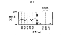
- FIG. 7 is a graph showing the relationship between the wavelength of incident light and the reflectance in the optical apparatus shown in FIG.
- an optical device 101 that includes an optical element 111 inside and causes signal light to enter the optical element 111 from an optical window.
- the optical element 111 is fixed to the bottom of a rectangular container-like casing 112, and the casing 112 is sealed by a lid 113 joined on the casing 112.
- Signal light is incident on the optical element 111 from an optical window 113 a formed in the lid 113.
- Patent Document 1 for example.
- the optical window 113a of the optical device 101 may be provided with antireflection films 115 and 116 that suppress reflection of signal light to be used.
- the antireflection films 115 and 116 as shown in FIG. 7, the correspondence to light having a wavelength in the visible light region is not considered in design.
- the presence or absence of foreign matter remaining in the optical device 101 is inspected in a state where the lid portion 113 is bonded to the housing portion 112.
- an inspection apparatus having an observation optical system is used, and the inspection apparatus determines the presence or absence of foreign matter at the in-focus position of the observation optical system.
- the observation optical system has a depth of field determined by the optical magnification, the numerical aperture (NA), and the specification of the image sensor.
- NA numerical aperture
- the depth of field of the observation optical system is made shallow, and for example, adjustment is made so that the focus is limited only to a range thinner than the thickness of the optical window 113a.
- the observation optical system cannot focus on the outer surface (outer surface) of the optical window 113a and the inside of the lid portion 113 at the same time. Therefore, it can be determined that the foreign matter observed when the observation optical system is focused on the outer surface of the optical window 113a is present outside the optical window 113a. On the other hand, it can be determined that the foreign matter observed when the observation optical system is focused on the inner surface (inner surface) of the optical window 113a is present inside the optical window 113a.
- the presence / absence of the foreign matter and the position of the foreign matter in the optical device 101 are detected by moving the focus position of the observation optical system.
- Patent Document 2 discloses a method for detecting the positions of defects in the medium of the first surface, the second surface and the transparent plate of the transparent plate.
- the defect in the medium of the transparent plate is directly irradiated with light from the side surface of the transparent plate by internal illumination, and the external illumination is irradiated with light from a predetermined angle with respect to the normal direction of the transparent plate, Images are taken with the first defocus position and the second defocus position in focus. Further, by comparing the signal levels of the defects shown in these images, the height position of the defect in the transparent plate (the position of the defect in the normal direction of the transparent plate) is calculated.
- Japanese Patent Publication Japanese Patent Laid-Open No. 2006-128514 (published on May 18, 2006) Japanese Patent Gazette “Special Table 2001-198190 (published on October 23, 2001)"
- the foreign matter observed when the depth of field of the observation optical system is reduced and the observation optical system is focused on the outer surface of the optical window 113a is present outside the optical window 113a. It is determined that Further, it is determined that the foreign matter observed when the observation optical system is focused on the inner surface of the optical window 113a is present inside the optical window 113a. Further, it is determined that the foreign matter observed when the observation optical system is focused on the outer surface of the optical element 111 is present on the outer surface of the optical element 111.
- depth of field allowable scattering circle diameter / (NA ⁇ optical magnification).
- NA ⁇ optical magnification allowable scattering circle diameter / (NA ⁇ optical magnification).
- An optical system with a shallow depth of field has a high magnification.
- An optical system is easier to configure. For this reason, when it is necessary to observe a wide range with the observation optical system, it is necessary to repeatedly observe while moving the optical device 101 that is the observation target in a horizontal plane, which requires a long time for observation. .
- the configuration described in Patent Document 2 has an advantage that the height position of a foreign object can be measured from two images.
- an object of the present invention is to provide an optical element and an optical device, an inspection device for the optical element and the optical device, and an inspection method for the optical element and the optical device that can easily detect the presence of the foreign matter and the position of the foreign matter.
- the optical device of the present invention is an optical device comprising a housing part, an optical element housed in the housing part, and a lid part that has an optical window and closes the opening of the housing part.
- the optical window transmits the signal light used by the optical element, and the reflectance with respect to the inspection light having a wavelength different from that of the signal light is higher than the reflectance with respect to the signal light.
- a first antireflection film having a reflectance with respect to the inspection light lower than a reflectance with respect to the first inspection light as the inspection light is provided.
- the configuration of the present invention it is easy to detect the presence of foreign matter and the position of foreign matter in an optical device or optical element.
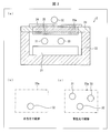
- FIG. 2A is a longitudinal sectional view of the optical device shown in FIG. 2B is an explanatory diagram showing a foreign object photographed by the camera shown in FIG. 1 when red light is irradiated from the upper surface of the optical device shown in FIG.
- FIG. 2C is an explanatory diagram showing a foreign object photographed by the camera shown in FIG. 1 when blue light is irradiated from the upper surface of the optical device shown in FIG.
- It is a graph which shows the relationship between the wavelength of incident light and the reflectance in the optical apparatus shown to (a) of FIG. It is a longitudinal cross-sectional view of the optical apparatus of other embodiment of this invention.
- Embodiment 1 Embodiments of the present invention will be described below with reference to the drawings.
- FIG. 1 is a block diagram showing the configuration of the inspection apparatus of the present embodiment.
- the inspection apparatus 1 includes a camera (imaging unit) 11, an illumination device (illumination unit) 12, a control unit 13, a storage unit 14, and a determination unit 15.
- the camera 11 is a conventionally known imaging device, for example, from a CCD camera.
- the camera 11 photographs the optical device 2 from the upper surface side, and acquires an image (image data) of the optical device 2.
- the acquired image is stored in the storage unit 14.
- the camera 11 acquires an image of the optical device 2 for each of a plurality of colors emitted by the illumination device 12.
- the illumination device 12 is, for example, provided in a ring shape around the camera 11.
- the illuminating device 12 includes LED illuminations of a plurality of colors, and when the camera 11 takes an image, the illuminating device 12 can select the color of the illumination that irradiates the optical device 2 that is a subject each time.
- the illumination device 12 can emit red light (first visible light (first inspection light)) and blue light (second visible light (second inspection light)). Yes.
- the control unit 13 controls the operation of each unit of the inspection device 1 and causes the storage unit 14 to store the image of the optical device 2 acquired by the camera 11.
- the storage unit 14 is a storage device made of, for example, a semiconductor memory.
- the determination unit 15 compares a plurality of images of the optical device 2 stored in the storage unit 14, and the presence / absence of foreign matter in the optical device 2 and the position of the foreign matter when the foreign matter is present (where the foreign matter exists in the optical device 2 And the size and shape of the foreign material.
- FIG. 2A is a longitudinal sectional view of the optical device 2 shown in FIG.
- FIG. 2B is an explanatory diagram showing a foreign object photographed by the camera 11 shown in FIG. 1 when red light is irradiated from the upper surface of the optical device 2.
- FIG. 2C is an explanatory diagram showing a foreign object photographed by the camera 11 shown in FIG. 1 when blue light is irradiated from the upper surface of the optical device 2.
- FIG. 3 is a graph showing the relationship between the wavelength of incident light and the reflectance in the optical device 2.
- an optical element 21 is fixed to the bottom of a rectangular container-like housing portion 22.
- a lid portion 23 is bonded onto the housing portion 22, thereby sealing the inside of the optical device 2.
- the lid portion 23 is formed with an optical window 23 a that transmits light incident on the optical element 21.
- a window portion antireflection film (first antireflection film) 24 is provided on the upper surface of the optical window 23a, and a window portion antireflection film (first antireflection film) 25 is provided on the lower surface of the optical window 23a. It has been.
- the window portion antireflection films 24 and 25 have a low reflectance with respect to the signal light (first wavelength light) used by the optical device 2, and the reflectance with respect to visible light (inspection light). Is high.
- the signal light is light having a wavelength of, for example, around 1550 nm.
- first visible light first inspection light
- second visible light second inspection light
- the first visible light is red light having a wavelength near 770 nm.
- the second visible light is blue light having a wavelength near 450 nm. Therefore, the wavelength characteristics of the window part antireflection films 24 and 25 included in the optical device 2 are summarized as follows.
- Signal light (Example) Light having a wavelength of around 1550 nm, low reflectance, transmitted through the window antireflection films 24 and 25 (incident into the optical device 3)
- Red light first visible light (first inspection light)
- example light having a wavelength of around 450 nm transmitted through the window part antireflection films 24 and 25.
- the specific reflectance of the window part antireflection films 24 and 25 is, for example, a reflectance of 1% for signal light.
- the reflectance for red light (first inspection light) is 80% or more, and the reflectance for blue light (second inspection light) is 40% or less.
- the window part antireflection films 24 and 25 have the same characteristics here, the window part antireflection film 24 may have a higher visible light reflectance than the window part antireflection film 25.
- the wavelength of the signal light is not limited to 1550 nm, and may be any wavelength of signal light that is actually used in the optical device 2.
- both of the window antireflection films 24 and 25 are necessary, only one of the reflection characteristics with respect to red light (first inspection light) and blue light (second inspection light) has. It only has to be.
- the manufacturing process of the optical apparatus 2 including the inspection process (foreign matter detection process) of the optical apparatus 2 by the inspection apparatus 1 in the above configuration will be described below.
- the lid portion 23 is joined to the housing portion 22 to seal the optical device 2.
- the lid part 23 is removed from the housing part 22, the inside of the optical device 2 is cleaned to remove the foreign substance, and then the lid part 23 is joined to the housing part 22. Then, the optical device 2 is sealed. Note that, after cleaning the inside of the optical device 2, the inspection by the inspection device 1 may be performed again before the lid portion 23 is joined to the housing portion 22.
- the optical system of the inspection apparatus 1, that is, the camera 11, has a deep depth of field, and can take an image from the outer surface of the optical window 23 a to the incident surface of the optical element 21 in a focused state.
- the shooting range by the camera 11 desirably includes the entire optical window 23a. However, when only a range narrower than the optical window 23a can be shot, the camera 11 or the optical device 2 is moved and the shooting of the optical device 2 is repeated. Thus, the entire area of the optical window 23a is photographed.
- the optical device 2 is irradiated with red light (first inspection light) from the illumination device 12.
- a first image is acquired by photographing.
- the control unit 13 stores the first image in the storage unit 14.
- the optical device 2 is irradiated with blue light (second inspection light) from the illumination device 12 without changing any positions such as the position of the inspection device 1 and the position of the optical device 2, and the camera 11
- the optical device 2 is photographed to acquire a second image.
- the control unit 13 stores the second image in the storage unit 14. Note that the order of obtaining the first image obtained by irradiating red light and the second image obtained by irradiating blue light may be first.
- the determination unit 15 compares the first image and the second image stored in the storage unit 14 to determine whether there is a foreign object in the optical device 2 and there is a foreign object in the optical device 2. If so, determine the size and shape of the foreign material.
- the red light is reflected by the window portion antireflection film 24.
- the blue light passes through the window part antireflection film 24 and the window part antireflection film 25 and is irradiated on the surface of the optical element 21. Therefore, as shown in FIG. 2A, when the foreign matter 31 and 33 are present inside the optical device 2 and the foreign matter 32 is present on the outer surface of the optical window 23a (the upper surface of the optical device 2), red light is emitted.
- the first image taken by irradiation includes only the foreign matter 32.
- the second image taken by irradiating blue light includes foreign substances 31 to 33.
- the determination unit 15 performs an operation of subtracting the first image (first image data) from the second image (second image data) to obtain a difference image (difference image data).
- the foreign matter 31 and 33 are included in the difference image, and therefore the determination unit 15 determines that there is a foreign matter inside the optical device 2.
- the determination unit 15 determines that no foreign object exists inside the optical device 2.
- the determination unit 15 obtains the size and shape of the foreign object from the coordinates of the foreign object.
- the inspection apparatus 1 outputs the determination result by the determination unit 15 as a foreign object detection result.
- the inspection apparatus 1 of the present embodiment In the inspection apparatus 1 of the present embodiment, the foreign matter between the outer surface of the optical window 23a of the optical apparatus 2 and the incident surface of the optical element 21 without changing the focal position of the camera 11 in accordance with the optical apparatus 2 to be inspected. The presence or absence can be inspected. As a result, the inspection apparatus 1 has a simple structure for inspecting the presence or absence of foreign matter in the optical apparatus 2 and can reduce the time required for this inspection.
- the camera 11 can observe the foreign matter in a state where it is focused on the foreign matter between the outer surface of the optical window 23a of the optical device 2 and the incident surface of the optical element 21, the camera 11 has acquired it.
- the size and shape of the foreign matter can be detected with high accuracy from the image of the optical device 2.
- the length of the long side (longer side) of the foreign matter is a case where a predetermined threshold or more (Amm or more) is impossible and a length less than a predetermined threshold (Amm) is allowed. Therefore, detecting the size and shape of a foreign object with an optical system having a deep depth of field can cope with such a situation.
- the light emitted from the illumination device 12 to the optical device 2 is red light (first visible light (first inspection light)) and blue light (second visible light (second visible light)
- the window part antireflection films 24 and 25 have a high visible light reflectivity and a blue light reflectivity lower than a red light reflectivity.
- the inspection light (first inspection light and second inspection light) that the illumination device 12 irradiates the optical device 2 is not limited to red light and blue light. That is, the inspection light (the first inspection light and the second inspection light) is light having a wavelength other than the wavelength of the signal light, and the first inspection light is reflected by the window portion antireflection films 24 and 25.
- the second inspection light has a low reflectance at the window portion antireflection films 24 and 25.
- the reflectance of the window part antireflection films 24 and 25 may be set in accordance with the first and second inspection lights.
- the light from the illumination device 12 may be irradiated to the optical device 2 via a diffusion plate.
- the illuminating device 12 includes LED lighting of a plurality of colors, and includes red light (first visible light (first inspection light)) and blue light (second visible light (second inspection light).
- the optical device 2 is irradiated with green light (third visible light (third inspection light)).
- Green light is light having a wavelength near 530 nm.
- the camera 11 acquires a third image by the green light in addition to the first image by the red light and the second image by the blue light.
- the determination unit 15 compares the first image, the second image, and the third image of the optical device 2 stored in the storage unit 14, and the presence or absence of foreign matter in the optical device 3 and the presence of foreign matter are present. The position of the foreign matter (where the foreign matter is present in the optical device 3), and the size and shape of the foreign matter are obtained.
- FIG. 4 is a longitudinal sectional view of the optical device 3 of the present embodiment.
- FIG. 5 is a graph showing the relationship between the wavelength of incident light and the reflectance in the optical device 3.
- the optical device 3 includes an element portion antireflection film (second antireflection film) 26 in addition to the window portion antireflection films 24 and 25 included in the optical device 2.
- the element portion antireflection film 26 is provided on the incident surface of the optical element 21.
- the optical element 21 is, for example, a photodetector (PD) or a liquid crystal optical switch element (LCOS (Liquid crystal on silicon)
- an antireflection film may be provided on the incident surface of the optical element 21.
- Other configurations of the optical device 3 are the same as those of the optical device 2.
- the element portion antireflection film 26 reflects red light (first visible light (first inspection light)) and blue light (second visible light (second inspection light)), while signal light and green light. Transmits light (third visible light (third inspection light)). Therefore, the wavelength characteristics of the window part antireflection films 24 and 25 and the element part antireflection film 26 included in the optical device 3 are as follows.
- Signal light (Example) Light having a wavelength near 1550 nm, low reflectivity, transmitted through the window part antireflection films 24 and 25 and the element part antireflection film 26 (incident into the optical device 3)
- Red light first visible light (first inspection light)
- Blue light second visible light (second inspection) Light)
- example light having a wavelength near 450 nm, transmitted through the window portion antireflection films 24 and 25, and reflected by the element portion antireflection film 26.
- Green light third visible light (third inspection light), (example) )
- Light having a wavelength of around 530 nm nm transmitted through the window part antireflection films 24 and 25 and the element part antireflection film 26 (incident into the optical element 21)
- the specific reflectivities of the window antireflection films 24 and 25 are, for example, a reflectivity for signal light of 1% or less and a reflectivity for red light (first inspection light) of 80% or more.
- the reflectance for blue light (second inspection light) is 40% or less.
- the specific reflectance of the element portion antireflection film 26 is, for example, a reflectance for blue light of 80% or more and a reflectance for green light of 40% or less.
- the inspection apparatus 1 in the same manner as in the optical apparatus 2, the presence / absence of a foreign substance in the optical apparatus 3 and the size and shape of the foreign substance when the foreign substance exists in the optical apparatus 2 are obtained.
- the inspection apparatus 1 irradiates green light (third inspection light), takes an image of the optical apparatus 3 with the camera 11, and takes a third image of the optical apparatus 3 (inside the optical element 21). Image).
- the control unit 13 stores the third image in the storage unit 14.
- the determination unit 15 compares the second image and the third image stored in the storage unit 14 to obtain the presence / absence of a foreign substance in the optical element 21.
- the second image taken by irradiating the blue light includes the foreign objects 35 and 36. If the foreign material 34 exists inside the optical element 21, the third image captured by irradiating the green light includes the foreign materials 34 to 36.
- the determination unit 15 obtains a second difference image (difference image data) by performing an operation of subtracting the second image (second image data) from the third image (third image data).
- the determination unit 15 determines that there is a foreign matter inside the optical element 21.
- the determination unit 15 determines that there is no foreign object inside the optical element 21.
- the determination unit 15 obtains the size and shape of the foreign object from the coordinates of the foreign object.
- the inspection apparatus 1 outputs the determination result by the determination unit 15 as a foreign object detection result.
- the presence or absence of foreign matter in the optical element 21 is inspected in a state where the optical element 21 is housed in the optical device 2.
- the optical device 21 is photographed by directly irradiating the optical element 21 with blue light (here, the first inspection light) from the illumination device 12.
- blue light here, the first inspection light
- an image of the optical element 21 here, the first image
- green light herein, the second inspection light
- the image of the optical element 21 (here, the second image) may be acquired by photographing the image 21, and the presence or absence of a foreign substance in the optical element 21 may be determined from the first image and the second image.
- the inspection method in this case is the same as that performed for the optical devices 2 and 3.
- the third inspection light can be used to inspect whether there is an abnormality in the optical element 21 compared to a normal product. It is possible to use a third image alone taken by irradiation.
- the optical device of the present invention is an optical device comprising a housing part, an optical element housed in the housing part, and a lid part that has an optical window and closes the opening of the housing part.
- the optical window transmits the signal light used by the optical element, and the reflectance with respect to the inspection light having a wavelength different from that of the signal light is higher than the reflectance with respect to the signal light.
- a first antireflection film having a reflectance with respect to the inspection light lower than a reflectance with respect to the first inspection light as the inspection light is provided.
- the first antireflection film provided on the optical window transmits the signal light used by the optical element and reflects the first and second inspection lights having wavelengths different from the signal light.
- the reflectance is higher than the reflectance for the signal light, and the reflectance for the second inspection light is lower than the reflectance for the first inspection light.
- the first inspection light is set to a wavelength that is substantially reflected by the first antireflection film, for example
- the second inspection light is set to a wavelength that is substantially transmitted through the first antireflection film, for example.
- the first image of the optical device photographed by irradiating the first inspection light includes: Foreign matter existing outside the optical device is included, and foreign matter existing inside the optical device is not included.
- the second image of the optical device photographed by irradiating the second inspection light includes foreign matter existing outside and inside the optical device.
- the first difference image includes only foreign substances existing inside the optical device. Thereby, the presence or absence of a foreign substance in the optical device can be inspected.
- the first antireflection film has a reflectance with respect to the signal light of 1% or less, a reflectance with respect to the first inspection light of 80% or more, and the second inspection light.
- the reflectance may be 40% or less.
- the reflectance of the first antireflection film is such that the reflectance with respect to the signal light and the reflectance with respect to the first and second inspection lights are based on the signal light.
- it is appropriate for inspecting the presence or absence of foreign matter inside the optical device based on the first and second inspection lights.
- a second antireflection which has a reflectance for the third inspection light as the inspection light lower than a reflectance for the second inspection light on the incident surface of the signal light of the optical element. It is good also as a structure provided with the film
- inspection light becomes lower than the reflectance with respect to 2nd test
- the second inspection light is set to a wavelength that is substantially transmitted through the first antireflection film and substantially reflected by the second antireflection film
- the third inspection light is, for example, the third antireflection film
- the second inspection light is irradiated when foreign matter is present outside the optical element (the upper surface of the incident surface of the optical element or above the incident surface) and inside the optical element.
- the second image of the optical device photographed in this manner includes foreign matter existing outside the optical device and inside the optical device (outside the optical element), and includes foreign matter existing inside the optical element. Absent.
- the third image of the optical device photographed by irradiating the second inspection light includes foreign matter existing outside the optical device, inside the optical device (outside the optical element), and inside the optical element. It is.
- the second difference image includes only the foreign matter existing inside the optical element. Thereby, the presence or absence of a foreign substance inside the optical element can be further inspected.
- the first antireflection film has a reflectance with respect to the signal light of 1% or less, a reflectance with respect to the first inspection light of 80% or more, and the second and third components.
- the second antireflection film has a reflectance of 1% or less for the signal light and a reflectance for the second inspection light of 80% or more.
- the reflectance for the third inspection light may be 40% or less.
- the reflectance of the first and second antireflection films is such that the reflectance with respect to the signal light and the reflectance with respect to the first to third inspection lights are based on the signal light.
- the presence or absence of foreign matter inside the optical device is inspected based on the first and second inspection lights, and the presence or absence of foreign matter inside the optical element is inspected based on the second and third inspection lights.
- the optical element of the present invention is an optical element having an incident surface for signal light, wherein the signal light is transmitted through the incident surface, and reflectivity for inspection light having a wavelength different from that of the signal light is reflected to the signal light.
- An antireflection film having a higher reflectance than the reflectance of the second inspection light as the inspection light and lower than the reflectance of the first inspection light as the inspection light is provided.
- the antireflection film provided on the incident surface transmits the signal light, and the reflectivity for the first and second inspection lights having a wavelength different from that of the signal light is higher than the reflectivity for the signal light.
- the reflectance for the second inspection light is lower than the reflectance for the first inspection light.
- the first inspection light is set to a wavelength that is substantially reflected by the first antireflection film, for example
- the second inspection light is set to a wavelength that is substantially transmitted through the first antireflection film, for example.
- the first image of the optical element photographed by irradiating the first inspection light includes: Foreign matter existing outside the optical element is included, and foreign matter existing inside the optical element is not included.
- the second image of the optical element photographed by irradiating the second inspection light includes foreign matters existing outside and inside the optical element.
- the first difference image obtained by subtracting the first image from the second image is acquired, the first difference image includes only foreign substances existing inside the optical element. Thereby, the presence or absence of a foreign substance in the optical element can be inspected.
- the antireflection film has a reflectance of 1% or less for the signal light, a reflectance of 80% or more for the inspection light, and a reflectance of 40% or less for the inspection light. It is good also as a structure.
- the reflectance of the antireflection film is such that the reflectance with respect to the signal light and the reflectance with respect to the first and second inspection lights are based on the operation of the optical element based on the signal light. This is appropriate for inspecting the presence or absence of foreign matter inside the optical element based on the first and second inspection lights.
- An inspection apparatus for an optical device includes an illumination unit that irradiates the first and second inspection lights in a direction from the optical window of the optical device according to claim 1 to the inside of the optical device.
- the optical device is photographed from the direction facing the optical window, and the optical device is photographed in a state where the first inspection light is irradiated to obtain a first image, and the second inspection light is obtained.
- photographs an optical apparatus from the direction facing an optical window
- inspection light and acquires a 1st image
- the optical device is photographed in a state where the second inspection light is irradiated to obtain a second image.
- the determination unit determines the presence / absence of a foreign substance in the optical device from the first image and the second image.
- the first inspection light is set to a wavelength that is substantially reflected by the first antireflection film, for example
- the second inspection light is set to a wavelength that is substantially transmitted through the first antireflection film, for example.
- the first image of the optical device photographed by irradiating the first inspection light includes: Foreign matter existing outside the optical device is included, and foreign matter existing inside the optical device is not included.
- the second image of the optical device photographed by irradiating the second inspection light includes foreign matter existing outside and inside the optical device.
- the first difference image includes only foreign substances existing inside the optical device. Thereby, the presence or absence of a foreign substance in the optical device can be inspected.
- An inspection apparatus for an optical device includes an illumination unit that irradiates the first and second inspection lights in a direction from the optical window of the optical device according to claim 3 or 4 toward the inside of the optical device.
- the optical device is photographed from the direction facing the optical window, and the optical device is photographed in a state where the first inspection light is irradiated to obtain a first image, and the second inspection light is obtained.
- a photographing unit that photographs the optical device in a state of being irradiated to acquire a second image, a storage unit that stores the first and second images, the first image, and the second image
- a determination unit that determines the presence / absence of foreign matter in the optical device from an image.
- photographs an optical apparatus from the direction facing an optical window
- inspection light and acquires a 1st image
- the optical device is photographed in a state where the second inspection light is irradiated to obtain a second image.
- the determination unit determines the presence / absence of a foreign substance in the optical device from the first image and the second image.
- the first inspection light is set to a wavelength that is substantially reflected by the first antireflection film, and the second inspection light is substantially transmitted through the first antireflection film, for example.
- the wavelength is set so as to be substantially reflected by the antireflection film.
- the first difference image includes only foreign substances existing inside the optical device. Therefore, the presence or absence of a foreign substance in the optical device can be inspected with higher accuracy.
- the inspection apparatus for an optical device irradiates the first, second, and third inspection lights in a direction from the optical window of the optical device according to claim 3 or 4 toward the inside of the optical device.
- the optical device is photographed from a direction facing the illumination unit and the optical window, the first image is obtained by photographing the optical device in a state where the first inspection light is irradiated, and the second A second image is obtained by photographing the optical device in a state where the inspection light is irradiated, and a third image is obtained by photographing the optical device in a state where the third inspection light is irradiated.
- An imaging unit to be acquired a storage unit for storing the first to third images, a presence / absence of a foreign substance in the optical device is determined from the first image and the second image, and the second A determination of the presence or absence of foreign matter in the optical element from the image and the third image A configuration that includes and.
- photographs an optical apparatus from the direction facing an optical window
- inspection light and acquires a 1st image
- a second image is obtained by photographing the optical device in a state irradiated with the second inspection light
- a third image is obtained by photographing the optical device in a state irradiated with the third inspection light.
- the determination unit determines the presence / absence of foreign matter inside the optical device from the first image and the second image, and determines the presence / absence of foreign matter inside the optical element from the second image and the third image.
- the first inspection light is set to a wavelength that is substantially reflected by the first antireflection film, and the second inspection light is substantially transmitted through the first antireflection film, for example.
- the wavelength that is substantially reflected by the antireflection film is set, and the third inspection light is set to a wavelength that substantially transmits the second antireflection film, for example.
- the second of the optical device that is imaged by irradiating the second inspection light
- the image includes foreign matter existing outside the optical device and inside the optical device (outside the optical element), and does not include foreign matter existing inside the optical element.
- the third image of the optical device photographed by irradiating the third inspection light includes foreign matter existing outside the optical device, inside the optical device (outside the optical element), and inside the optical element. It is.
- the first difference image includes only foreign substances existing inside the optical device.
- the second difference image includes only the foreign matter existing inside the optical element. Accordingly, it is possible to inspect for the presence or absence of foreign matter inside the optical device and the presence or absence of foreign matter inside the optical element.
- the inspection light may be visible light.
- the illumination unit can be easily configured using a general-purpose light source.
- An inspection apparatus for an optical device includes: an illumination unit that irradiates the first and second inspection lights in a direction from the incident surface of the optical element according to claim 5 toward the inside of the optical element; The optical element is photographed from a direction facing the incident surface, and the first image is obtained by photographing the optical element in a state where the first inspection light is irradiated, and the second inspection light is irradiated.
- the imaging unit that captures the optical element to acquire the second image
- the storage unit that stores the first image and the second image, the first image, and the second image
- a determination unit that determines the presence or absence of a foreign substance inside the optical element from the image.
- photographs an optical element from the direction which opposes an entrance plane
- inspection light and acquires a 1st image
- the second image is acquired by photographing the optical element in a state where the second inspection light is irradiated.
- the determination unit determines the presence or absence of a foreign substance inside the optical element from the first image and the second image.
- the first inspection light is set to a wavelength that is substantially reflected by the antireflection film, for example, and the second inspection light is set to a wavelength that substantially transmits the antireflection film, for example, the outside of the optical element ( In the case where foreign matter is present on the upper surface of the optical window or above the optical window) and inside the optical element, the first image of the optical element photographed by irradiating the first inspection light is present outside the optical element. Foreign substances that are present inside the optical element are not included.
- the second image of the optical element photographed by irradiating the second inspection light includes foreign matters existing outside and inside the optical device element.
- the first difference image obtained by subtracting the first image from the second image is acquired, the first difference image includes only foreign substances existing inside the optical element. Thereby, the presence or absence of a foreign substance in the optical element can be inspected.
- An inspection method for an optical device includes an illumination step of irradiating the first and second inspection lights in a direction from the optical window of the optical device according to claim 1 or 2 toward the inside of the optical device.
- the optical device is photographed from the direction facing the optical window, and the optical device is photographed in a state where the first inspection light is irradiated to obtain a first image, and the second inspection light is obtained.
- An inspection method for an optical device includes an illumination step of irradiating the first and second inspection lights in a direction from the optical window of the optical device according to claim 3 or 4 toward the inside of the optical device.
- the optical device is photographed from the direction facing the optical window, and the optical device is photographed in a state where the first inspection light is irradiated to obtain a first image, and the second inspection light is obtained.
- An inspection method for an optical device irradiates the first, second, and third inspection lights in a direction from the optical window of the optical device according to claim 3 or 4 toward the inside of the optical device.
- Photographing the optical device from an illumination step and a direction facing the optical window photographing the optical device in a state where the first inspection light is irradiated, obtaining a first image, and obtaining the second image
- a second image is obtained by photographing the optical device in a state where the inspection light is irradiated
- a third image is obtained by photographing the optical device in a state where the third inspection light is irradiated.
- the imaging process to be acquired, the presence or absence of foreign matter inside the optical device is determined from the first image and the second image, and the inside of the optical element is determined from the second image and the third image. And a determination step of determining the presence or absence of foreign matter.
- An inspection method for an optical device includes an illumination step of irradiating the first and second inspection lights in a direction from the incident surface of the optical element according to claim 5 toward the inside of the optical element, The optical element is photographed from a direction facing the incident surface, and the first image is obtained by photographing the optical element in a state where the first inspection light is irradiated, and the second inspection light is irradiated.
Landscapes
- Physics & Mathematics (AREA)
- General Physics & Mathematics (AREA)
- Engineering & Computer Science (AREA)
- Biochemistry (AREA)
- Chemical & Material Sciences (AREA)
- General Health & Medical Sciences (AREA)
- Life Sciences & Earth Sciences (AREA)
- Immunology (AREA)
- Pathology (AREA)
- Health & Medical Sciences (AREA)
- Analytical Chemistry (AREA)
- Computer Vision & Pattern Recognition (AREA)
- Theoretical Computer Science (AREA)
- Quality & Reliability (AREA)
- Signal Processing (AREA)
- Multimedia (AREA)
- Investigating Materials By The Use Of Optical Means Adapted For Particular Applications (AREA)
- Photometry And Measurement Of Optical Pulse Characteristics (AREA)
- Surface Treatment Of Optical Elements (AREA)
- Light Receiving Elements (AREA)
- Optics & Photonics (AREA)
Abstract
異物の存在および異物の位置の検出を容易にする。光学装置(2)は、筐体部(22)の開口部を塞ぐ蓋部(23)の光学窓(23a)に、光学素子(21)が使用する信号光を透過させ、信号光とは波長が異なる検査光に対する反射率が信号光に対する反射率よりも高く、第2の検査光に対する反射率が第1の検査光に対する反射率よりも低い第1および第2の反射防止膜(24,25)が設けられている。
Description
本発明は、信号光を使用する光学素子および光学素子を備える光学装置、光学素子および光学装置の検査装置、並びに光学素子および光学装置の検査方法に関する。
図6は従来の光学装置の構成を示す縦断面図である。図7は、図6に示した光学装置における入射光の波長と反射率との関係を示すグラフである。
従来、図6に示すように、内部に光学素子111を備え、光学窓から光学素子111に信号光を入射させる光学装置101が知られている。光学装置101は、方形の容器状の筐体部112の底部に光学素子111が固定され、筐体部112の上に接合された蓋部113により、筐体部112が封止されている。光学素子111へは、蓋部113に形成された光学窓113aから信号光が入射する。このような光学装置101は、例えば特許文献1に示されている。
光学装置101の光学窓113aには、使用する信号光の反射を抑制する反射防止膜115,116が設けられることがある。反射防止膜115,116では、図7に示すように、設計上、可視光領域の波長の光への対応については考慮されていない。
光学装置101では、筐体部112に蓋部113を接合した状態にて、光学装置101の内部に残留している異物の有無が検査される。この検査には観察用光学系を有する検査装置を使用し、検査装置は、観察用光学系の合焦位置にて異物の有無を判定する。
観察用光学系は、光学倍率や開口数(NA)、撮像素子の仕様から定まる被写界深度を有し、物体が被写界深度に収まった場合、物体をはっきりとらえる。一方、物体が被写界深度から外れるほど、ピントがぼけて物体が見えなくなる。
検査装置では、従来、観察用光学系の被写界深度を浅くし、例えば光学窓113aの厚さよりも薄い範囲にしか焦点が合わないように調整する。この場合、観察用光学系は、光学窓113aの外面(外側の表面)と蓋部113の内部とに同時に合焦させることができない。したがって、観察用光学系を光学窓113aの外面に合焦させたときに観察された異物は、光学窓113aの外側に存在すると判断できる。一方、観察用光学系を光学窓113aの内面(内側の表面)に合焦させたときに観察された異物は、光学窓113aの内側に存在していると判断できる。さらに、観察用光学系を光学素子111の外面に合焦させたときに観察された異物は、光学素子111の外面に存在すると判断できる。このように、従来の検査装置では、観察用光学系の合焦位置を移動させていくことにより、光学装置101における異物の有無および異物の位置を検出するようにしている。
また、特許文献2には、透明板の第1の表面、第2の表面および透明板の媒質中の欠陥の位置を検知する方法が開示されている。この方法では、透明板の媒質中の欠陥に対し、直接内部照明により透明板の側面から光を照射し、かつ外部照明により透明板の法線方向に対して所定の角度から光を照射し、第1の焦点はずれ位置、および第2の焦点はずれ位置に焦点を合わせて、それぞれ画像を撮影している。さらに、これら画像に示される欠陥の信号レベルを比較することにより、透明板における欠陥の高さ位置(透明板の法線方向における欠陥の位置)を算出するようにしている。
上記従来の検査装置では、観察用光学系の被写界深度を浅くし、観察用光学系を光学窓113aの外面に合焦させたときに観察された異物は、光学窓113aの外側に存在していると判定する。また、観察用光学系を光学窓113aの内面に合焦させたときに観察された異物は、光学窓113aの内側に存在している判定する。さらに、観察用光学系を光学素子111の外面に合焦させたときに観察された異物は、光学素子111の外面に存在すると判定している。
したがって、筐体部112に蓋部113を接合した後で、上記各部の異物の有無を検査する場合、各観察対象面に対して観察用光学系を正確に合焦させる必要がある。また、観察対象面が変わるたびに、観察用光学系の合焦位置の調整に伴い、検査装置や観察対象面の高さを調整する必要がある。このため、これらの作業が非常に面倒である。特に、観察対象が透明な光学窓113aである場合、光学窓113a自体に焦点を合わせることは容易ではない。
また、観察用光学系の被写界深度の理論式は、被写界深度=許容散乱円径/(NA×光学倍率)であり、一般に、被写界深度の浅い光学系は、倍率の高い光学系とする方が構成し易い。このため、観察用光学系により広い範囲を観察する必要がある場合には、観察対象である光学装置101を水平面内で移動させながら繰り返し観察する必要があり、観察に長時間を要することになる。
一方、特許文献2に記載の構成では、2枚の画像から異物の高さ位置を測定できるという利点がある。しかしながら、特許文献2に記載の構成では、2種類の照明をそれぞれ異なる状態に配置する必要があり、特に、直接内部照明については、検査対象に細工を施して取り付ける必要がある。このため、光学装置101に対しては容易に適用し難いという問題点を有している。
したがって、本発明は、異物の存在および異物の位置の検出が容易である光学素子および光学装置、光学素子および光学装置の検査装置、並びに光学素子および光学装置の検査方法の提供を目的としている。
本発明の光学装置は、筐体部と、前記筐体部に収納された光学素子と、光学窓を有し、前記筐体部の開口部を塞ぐ蓋部とを備えている光学装置において、前記光学窓には、前記光学素子が使用する信号光を透過させ、前記信号光とは波長が異なる検査光に対する反射率が前記信号光に対する反射率よりも高く、前記検査光としての第2の検査光に対する反射率が前記検査光としての第1の検査光に対する反射率よりも低い第1の反射防止膜が設けられていることを特徴としている。
本発明の構成によれば、光学装置や光学素子における異物の存在および異物の位置の検出が容易である。
〔実施形態1〕
本発明の実施形態を図面に基づいて以下に説明する。
本発明の実施形態を図面に基づいて以下に説明する。
(検査装置1の構成)
図1は、本実施形態の検査装置の構成を示すブロック図である。図1に示すように、検査装置1は、カメラ(撮影部)11、照明装置(照明部)12、制御部13、記憶部14および判定部15を備えている。
図1は、本実施形態の検査装置の構成を示すブロック図である。図1に示すように、検査装置1は、カメラ(撮影部)11、照明装置(照明部)12、制御部13、記憶部14および判定部15を備えている。
カメラ11は、従来周知の撮像装置であり、例えばCCDカメラからである。カメラ11は、光学装置2を上面側から撮影し、光学装置2の画像(画像データ)を取得する。取得した画像は記憶部14へ格納する。この場合、カメラ11は、照明装置12が照射する複数の複数の色ごとに光学装置2の画像を取得する。
照明装置12は、例えば、カメラ11の周囲にリング状に設けられたものである。照明装置12は、複数の色のLED照明を備え、カメラ11が撮影するときに、被写体である光学装置2に照射する照明の色をその都度選択できるようになっている。本実施形態において、照明装置12は、赤色光(第1の可視光(第1の検査光))および青色光(第2の可視光(第2の検査光))を照射できるようになっている。
制御部13は、検査装置1の各部の動作を制御し、カメラ11が取得した光学装置2の画像を記憶部14に記憶させる。記憶部14は、例えば半導体メモリからなる記憶装置である。
判定部15は、記憶部14が記憶している光学装置2の複数の画像を比較し、光学装置2における異物の有無、異物が存在する場合の異物の位置(光学装置2のどこに異物が存在するか)、並びに異物のサイズおよび形状を求める。
(光学装置2の構成)
図2の(a)は、図1に示した光学装置2の縦断面図である。図2の(b)は、光学装置2の上面から赤色光を照射した場合に図1に示したカメラ11にて撮影される異物を示す説明図である。図2の(c)は、光学装置2の上面から青色光を照射した場合に図1に示したカメラ11にて撮影される異物を示す説明図である。図3は、光学装置2における入射光の波長と反射率との関係を示すグラフである。
図2の(a)は、図1に示した光学装置2の縦断面図である。図2の(b)は、光学装置2の上面から赤色光を照射した場合に図1に示したカメラ11にて撮影される異物を示す説明図である。図2の(c)は、光学装置2の上面から青色光を照射した場合に図1に示したカメラ11にて撮影される異物を示す説明図である。図3は、光学装置2における入射光の波長と反射率との関係を示すグラフである。
図2の(a)に示すように、光学装置2は、例えば方形の容器状の筐体部22の底部に光学素子21が固定されている。筐体部22の上には蓋部23が接合され、これにより光学装置2の内部が封止されている。蓋部23には、光学素子21への入射光を透過する光学窓23aが形成されている。
光学窓23aの上面には、窓部反射防止膜(第1の反射防止膜)24が設けられ、光学窓23aの下面には、窓部反射防止膜(第1の反射防止膜)25が設けられている。窓部反射防止膜24,25は、光学装置2が使用する信号光(第1の波長の光)については、反射率が低くなっており、可視光(検査光)に対しては、反射率が高くなっている。
本実施形態において、信号光は、波長が例えば1550nm付近の光である。可視光については、第1の可視光(第1の検査光)と第2の可視光(第2の検査光)とを使用する。第1の可視光は、波長が770nm付近の赤色光である。第2の可視光は、波長が450nm付近の青色光である。したがって、光学装置2が備える窓部反射防止膜24,25の波長特性をまとめると次のようになる。
信号光:(例)波長1550nm付近の光、反射率が低、窓部反射防止膜24,25を透過(光学装置3の内部へ入射)
赤色光:第1の可視光(第1の検査光)、(例)波長770nm付近の光、窓部第反射防止膜24,25にて反射
青色光:第2の可視光(第2の検査光)、(例)波長450nm付近の光、窓部反射防止膜24,25を透過
なお、窓部反射防止膜24,25の具体的な反射率は、例えば、信号光に対する反射率が1%以下であり、赤色光(第1の検査光)に対する反射率が80%以上であり、青色光(第2の検査光)に対する反射率が40%以下である。
赤色光:第1の可視光(第1の検査光)、(例)波長770nm付近の光、窓部第反射防止膜24,25にて反射
青色光:第2の可視光(第2の検査光)、(例)波長450nm付近の光、窓部反射防止膜24,25を透過
なお、窓部反射防止膜24,25の具体的な反射率は、例えば、信号光に対する反射率が1%以下であり、赤色光(第1の検査光)に対する反射率が80%以上であり、青色光(第2の検査光)に対する反射率が40%以下である。
また、ここでは窓部反射防止膜24,25を同じ特性のものとしているが、窓部反射防止膜24は、窓部反射防止膜25よりも可視光の反射率が高くなっていてもよい。また、信号光の波長は、1550nmに限らず、光学装置2において実際に使用される信号光の波長であればよい。また、窓部反射防止膜24,25は、いずれも必要であるものの、赤色光(第1の検査光)および青色光(第2の検査光)に対する反射特性は、いずれか一方のみが有していればよい。
上記の構成において、検査装置1による光学装置2の検査工程(異物検出工程)を含む光学装置2の製造工程について以下に説明する。
(光学装置2の製造工程)
光学装置2の製造工程では、筐体部22の底部に光学素子21を固定した状態とする。この状態において、筐体部22の上に蓋部23を配置し、蓋部23を筐体部22に接合して光学装置2を封止する前に、検査装置1により光学装置2の内部における異物の有無を検査する。
光学装置2の製造工程では、筐体部22の底部に光学素子21を固定した状態とする。この状態において、筐体部22の上に蓋部23を配置し、蓋部23を筐体部22に接合して光学装置2を封止する前に、検査装置1により光学装置2の内部における異物の有無を検査する。
検査装置1による検査の結果、光学装置2の内部に異物が存在しなければ、蓋部23を筐体部22に接合して、光学装置2を封止する。一方、光学装置2の内部に異物が存在すれば、筐体部22から蓋部23を取り外し、光学装置2の内部を清掃して異物を除去した後、蓋部23を筐体部22に接合して光学装置2を封止する。なお、光学装置2の内部の清掃後、蓋部23を筐体部22に接合する前に、検査装置1による検査を再度行ってもよい。
また、蓋部23の上に載っている異物は後から除去が可能なため、ここでは問題とならない。すなわち、光学窓23aの内面や光学素子21の上面すなわち入射面に付着している異物のみを検出すればよい。
(光学装置2の検査工程)
検査装置1の光学系すなわちカメラ11は、被写界深度が深く設定され、光学窓23aの外面から光学素子21の入射面までを合焦状態にとして撮影が可能なものである。カメラ11による撮影範囲は、光学窓23aの全域を含むことが望ましいが、光学窓23aよりも狭い範囲しか撮影できない場合は、カメラ11あるいは光学装置2を移動させて、光学装置2の撮影を繰り返すことにより光学窓23aの全域を撮影する。
検査装置1の光学系すなわちカメラ11は、被写界深度が深く設定され、光学窓23aの外面から光学素子21の入射面までを合焦状態にとして撮影が可能なものである。カメラ11による撮影範囲は、光学窓23aの全域を含むことが望ましいが、光学窓23aよりも狭い範囲しか撮影できない場合は、カメラ11あるいは光学装置2を移動させて、光学装置2の撮影を繰り返すことにより光学窓23aの全域を撮影する。
検査においては、カメラ11と光学装置2との位置関係を調整した後、まず、照明装置12から赤色光(第1の検査光)を光学装置2に照射し、カメラ11にて光学装置2を撮影して第1の画像を取得する。制御部13は、第1の画像を記憶部14に格納する。
次に、検査装置1の位置および光学装置2の位置等の一切の位置を変更することなく、照明装置12から青色光(第2の検査光)を光学装置2に照射し、カメラ11にて光学装置2を撮影して第2の画像を取得する。制御部13は、第2の画像を記憶部14に格納する。なお、赤色光を照射して取得する第1の画像と青色光を照射して取得する第2の画像との取得順序はどちらが先であってもよい。
次に、判定部15は、記憶部14に格納されている第1の画像と第2の画像とを比較して、光学装置2内における異物の有無、並びに光学装置2内に異物が存在する場合に、異物のサイズおよび形状を求める。
この場合、赤色光は、窓部反射防止膜24にて反射される。一方、青色光は、窓部反射防止膜24および窓部反射防止膜25を透過して、光学素子21の表面に照射される。したがって、図2の(a)に示すように、光学装置2の内部に異物31および33が存在し、光学窓23aの外面(光学装置2の上面)に異物32が存在する場合、赤色光を照射して撮影された第1の画像には、図2の(b)に示すように、異物32のみが含まれる。一方、青色光を照射して撮影された第2の画像には、図2の(b)に示すように、異物31~33が含まれる。
そこで、判定部15は、第2の画像(第2の画像データ)から第1の画像(第1の画像データ)を差し引く演算を行って差分画像(差分画像データ)を取得する。図2の(a)~(c)の例では、差分画像に異物31,33が含まれるので、判定部15は、光学装置2の内部に異物が存在すると判定する。一方、差分画像に異物が含まれていない場合、判定部15は、光学装置2の内部に異物が存在しないと判定する。また、判定部15は、光学装置2の内部に異物が存在する場合、異物の座標から異物のサイズおよび形状を求める。検査装置1は、判定部15による判定結果を異物の検出結果として出力する。
(検査装置1の利点)
本実施形態の検査装置1では、検査対象の光学装置2に合わせてカメラ11の焦点位置を変更することなく、光学装置2の光学窓23aの外面から光学素子21の入射面までの間における異物の有無を検査することができる。これにより、検査装置1は、光学装置2内部の異物の有無の検査のための構成が単純になり、かつこの検査に要する時間を短縮することができる。
本実施形態の検査装置1では、検査対象の光学装置2に合わせてカメラ11の焦点位置を変更することなく、光学装置2の光学窓23aの外面から光学素子21の入射面までの間における異物の有無を検査することができる。これにより、検査装置1は、光学装置2内部の異物の有無の検査のための構成が単純になり、かつこの検査に要する時間を短縮することができる。
光学装置2の光学窓23aの外面から光学素子21の入射面までの間における異物の有無について、カメラ11により異物に合焦した状態にて異物を観察することができるので、カメラ11が取得した光学装置2の画像から、異物のサイズおよび形状を高精度に検出することができる。
ここで、異物を検出した場合であっても、実際には、異物のサイズや形状によって、異物の存在が問題にならない場合と、異物の存在が問題になり、異物の除去が必要な場合とがある。例えば、異物の長辺(長い方の辺)の長さは、所定の閾値以上(Amm以上)を不可、所定の閾値未満(Amm未満)を可とするような場合である。したがって、被写界深度の深い光学系により、異物のサイズおよび形状を検出することは、このような事情に対応することができる。
なお、検査装置1では、照明装置12が光学装置2へ照射する光は、赤色光(第1の可視光(第1の検査光))、および青色光(第2の可視光(第2の検査光))とし、窓部反射防止膜24,25は、可視光の反射率が高く、青色光の反射率が赤色光の反射率よりも低い構成とした。しかしながら、照明装置12が光学装置2へ照射する検査光(第1の検査光および第2の検査光)は、赤色光および青色光に限定されない。すなわち、検査光(第1の検査光および第2の検査光)は、信号光の波長以外の波長の光であって、第1の検査光が窓部反射防止膜24,25での反射率が高く、第2の検査光が窓部反射防止膜24,25での反射率が低いものであればよい。この場合、窓部反射防止膜24,25の反射率を第1および第2の検査光に合わせて設定してもよい。
また、カメラ11が撮影する画像には、照明装置12の映り込みが起こり易くなるため、照明装置12の光を拡散板を介して光学装置2へ照射するようにしてもよい。
〔実施形態2〕
本発明の他の実施形態を図面に基づいて以下に説明する。
本発明の他の実施形態を図面に基づいて以下に説明する。
(検査装置1の構成)
本実施形態において、照明装置12は、複数の色のLED照明を備え、赤色光(第1の可視光(第1の検査光))および青色光(第2の可視光(第2の検査光))に加えて、緑色光(第3の可視光(第3の検査光))を光学装置2に照射する。緑色光は、波長が530nm付近の光である。
本実施形態において、照明装置12は、複数の色のLED照明を備え、赤色光(第1の可視光(第1の検査光))および青色光(第2の可視光(第2の検査光))に加えて、緑色光(第3の可視光(第3の検査光))を光学装置2に照射する。緑色光は、波長が530nm付近の光である。
第1から第3の検査光に対応し、カメラ11は、赤色光による第1の画像、および青色光による第2の画像に加えて、緑色光による第3の画像を取得する。また、判定部15は、記憶部14が記憶している光学装置2の第1の画像、第2の画像および第3の画像を比較し、光学装置3における異物の有無、異物が存在する場合の異物の位置(光学装置3のどこに異物が存在するか)、並びに異物のサイズおよび形状を求める。
(光学装置3の構成)
図4は、本実施形態の光学装置3の縦断面図である。図5は、光学装置3における入射光の波長と反射率との関係を示すグラフである。
図4は、本実施形態の光学装置3の縦断面図である。図5は、光学装置3における入射光の波長と反射率との関係を示すグラフである。
光学装置3は、光学装置2が備える窓部反射防止膜24,25に加えて、素子部反射防止膜(第2の反射防止膜)26を備えている。素子部反射防止膜26は、光学素子21の入射面に設けられている。このように、光学素子21が例えばフォトディテクタ(PD)や液晶光スイッチ素子(LCOS(Liquid crystal on silicon))である場合には、光学素子21の入射面に反射防止膜が設けられることがある。光学装置3の他の構成は、光学装置2と同様である。
素子部反射防止膜26は、赤色光(第1の可視光(第1の検査光))および青色光(第2の可視光(第2の検査光))を反射する一方、信号光および緑色光(第3の可視光(第3の検査光))を透過する。したがって、光学装置3が備える窓部反射防止膜24,25および素子部反射防止膜26の波長特性は次のようになる。
信号光:(例)波長1550nm付近の光、反射率が低、窓部反射防止膜24,25および素子部反射防止膜26を透過(光学装置3の内部へ入射)
赤色光:第1の可視光(第1の検査光)、(例)波長770nm付近の光、窓部第反射防止膜24,25にて反射
青色光:第2の可視光(第2の検査光)、(例)波長450nm付近の光、窓部反射防止膜24,25を透過、素子部反射防止膜26にて反射
緑色光:第3の可視光(第3の検査光)、(例)波長530nmnm付近の光、窓部反射防止膜24,25および素子部反射防止膜26を透過(光学素子21の内部へ入射)
なお、窓部反射防止膜24,25の具体的な反射率は、例えば、信号光に対する反射率が1%以下であり、赤色光(第1の検査光)に対する反射率が80%以上であり、青色光(第2の検査光)に対する反射率が40%以下である。また、素子部反射防止膜26の具体的な反射率は、例えば、青色光に対する反射率が80%以上であり、緑色光に対する反射率が40%以下である。
赤色光:第1の可視光(第1の検査光)、(例)波長770nm付近の光、窓部第反射防止膜24,25にて反射
青色光:第2の可視光(第2の検査光)、(例)波長450nm付近の光、窓部反射防止膜24,25を透過、素子部反射防止膜26にて反射
緑色光:第3の可視光(第3の検査光)、(例)波長530nmnm付近の光、窓部反射防止膜24,25および素子部反射防止膜26を透過(光学素子21の内部へ入射)
なお、窓部反射防止膜24,25の具体的な反射率は、例えば、信号光に対する反射率が1%以下であり、赤色光(第1の検査光)に対する反射率が80%以上であり、青色光(第2の検査光)に対する反射率が40%以下である。また、素子部反射防止膜26の具体的な反射率は、例えば、青色光に対する反射率が80%以上であり、緑色光に対する反射率が40%以下である。
(光学装置3の検査工程)
上記の構成において、検査装置1による光学装置3の検査工程(異物検出工程)について以下に説明する。
上記の構成において、検査装置1による光学装置3の検査工程(異物検出工程)について以下に説明する。
検査装置1では、光学装置2の場合と同様にして、光学装置3内における異物の有無、並びに光学装置2内に異物が存在する場合に、異物のサイズおよび形状を求める。
また、青色光(第2の検査光)は、光学素子21の入射面の素子部反射防止膜26にて反射されるので青色光を照射した状態での光学装置3の撮影では、光学素子21の内部を観察できない。そこで、本実施形態において、検査装置1は、緑色光(第3の検査光)を照射し、カメラ11にて光学装置3を撮影して光学装置3の第3の画像(光学素子21の内部の画像)を取得する。制御部13は、第3の画像を記憶部14に格納する。
次に、判定部15は、記憶部14に格納されている第2の画像と第3の画像とを比較して、光学素子21内における異物の有無を求める。
この場合、図4に示すように、光学素子21の入射面に異物35,36が存在すれば、青色光を照射して撮影された第2の画像には、異物35,36が含まれる。また、光学素子21の内部に異物34が存在すれば、緑色光を照射して撮影された第3の画像には、異物34~36が含まれる。
そこで、判定部15は、第3の画像(第3の画像データ)から第2の画像(第2の画像データ)を差し引く演算を行って第2の差分画像(差分画像データ)を取得する。図4の例では、第2の差分画像に異物34が含まれるので、判定部15は、光学素子21の内部に異物が存在すると判定する。一方、第2の差分画像に異物が含まれていない場合、判定部15は、光学素子21の内部に異物が存在しないと判定する。また、判定部15は、光学素子21の内部に異物が存在する場合、異物の座標から異物のサイズおよび形状を求める。検査装置1は、判定部15による判定結果を異物の検出結果として出力する。
(検査装置1の利点)
本実施形態の検査装置1では、光学装置3の内部における異物の有無に加えて、光学素子21の内部における異物の有無を検査することができる。光学装置3の他の利点は、光学装置2と同様である。
本実施形態の検査装置1では、光学装置3の内部における異物の有無に加えて、光学素子21の内部における異物の有無を検査することができる。光学装置3の他の利点は、光学装置2と同様である。
なお本実施形態では、光学素子21を光学装置2の内部に収納した状態にて光学素子21の内部における異物の有無を検査した。しかしながら、光学素子21を光学装置2に収納する前の状態にて、照明装置12から光学素子21に対して直接に青色光(ここでは第1の検査光)を照射して光学素子21を撮影することにより、光学素子21の画像(ここでは第1の画像)を取得し、照明装置12から光学素子21に対して直接に緑色光(ここでは第2の検査光)を照射して光学素子21を撮影することにより、光学素子21の画像(ここでは第2の画像)を取得し、これら第1の画像および第2の画像から光学素子21内における異物の有無を判定してもよい。この場合の検査方法は、光学装置2,3に対して行ったものと同様である。また、ここでは画像の比較から光学素子21内部の異物を検知する方法について述べているが、光学素子21内部に正常品と比較して異常がないかを検査したい場合は、第3の検査光を照射して撮影された第3の画像単体を利用することができる。
〔まとめ〕
本発明の光学装置は、筐体部と、前記筐体部に収納された光学素子と、光学窓を有し、前記筐体部の開口部を塞ぐ蓋部とを備えている光学装置において、前記光学窓には、前記光学素子が使用する信号光を透過させ、前記信号光とは波長が異なる検査光に対する反射率が前記信号光に対する反射率よりも高く、前記検査光としての第2の検査光に対する反射率が前記検査光としての第1の検査光に対する反射率よりも低い第1の反射防止膜が設けられている構成である。
本発明の光学装置は、筐体部と、前記筐体部に収納された光学素子と、光学窓を有し、前記筐体部の開口部を塞ぐ蓋部とを備えている光学装置において、前記光学窓には、前記光学素子が使用する信号光を透過させ、前記信号光とは波長が異なる検査光に対する反射率が前記信号光に対する反射率よりも高く、前記検査光としての第2の検査光に対する反射率が前記検査光としての第1の検査光に対する反射率よりも低い第1の反射防止膜が設けられている構成である。
上記の構成によれば、光学窓に設けられている第1の反射防止膜は、光学素子が使用する信号光を透過させ、信号光とは波長が異なる第1および第2の検査光に対する反射率が信号光に対する反射率よりも高く、第2の検査光に対する反射率が第1の検査光に対する反射率よりも低くなっている。
したがって、第1および第2の検査光を照射して光学装置を観察することにより、光学装置の内部における異物の有無を検査することができる。
すなわち、第1の検査光は、例えば第1の反射防止膜にてほぼ反射される波長に設定し、第2の検査光は、例えば第1の反射防止膜をほぼ透過する波長に設定すれば、光学装置の外部(光学窓の上面または光学窓の上方)および光学装置の内部に異物が存在する場合、第1の検査光を照射して撮影される光学装置の第1の画像には、光学装置の外部に存在する異物が含まれ、光学装置の内部に存在する異物は含まれない。一方、第2の検査光を照射して撮影される光学装置の第2の画像には、光学装置の外部および内部に存在する異物が含まれる。
そこで、第2の画像から第1の画像を差し引いた第1の差分画像を取得すれば、第1の差分画像には光学装置の内部に存在する異物のみが含まれる。これにより、光学装置の内部における異物の有無を検査することができる。
上記の光学装置において、前記第1の反射防止膜は、前記信号光に対する反射率が1%以下であり、前記第1の検査光に対する反射率が80%以上であり、前記第2の検査光に対する反射率が40%以下である構成としてもよい。
上記の構成によれば、第1の反射防止膜の反射率は、信号光に対する反射率、並びに第1および記第2の検査光に対する反射率が、信号光に基づいて光学素子が動作する上、並びに第1および第2の検査光に基づいて光学装置の内部における異物の有無を検査する上において、適切となっている。
上記の光学装置において、前記光学素子の前記信号光の入射面には、前記検査光としての第3の検査光に対する反射率が前記第2の検査光に対する反射率よりも低い第2の反射防止膜が設けられている構成としてもよい。
上記の構成によれば、光学素子の信号光の入射面に設けられている第2の反射防止膜は、第3の検査光に対する反射率が第2の検査光に対する反射率よりも低くなっている。したがって、第2および第3の検査光を照射して光学装置を観察することにより、光学装置の内部に収納された光学素子の内部における異物の有無を検査することができる。
すなわち、第2の検査光は、例えば第1の反射防止膜をほぼ透過し、かつ第2の反射防止膜にてほぼ反射される波長に設定し、第3の検査光は、例えば第3の反射防止膜をほぼ透過する波長に設定すれば、光学素子の外部(光学素子の入射面の上面または入射面の上方)および光学素子の内部に異物が存在する場合、第2の検査光を照射して撮影される光学装置の第2の画像には、光学装置の外部、および光学装置の内部(光学素子の外部)に存在する異物が含まれ、光学素子の内部に存在する異物は含まれない。一方、第2の検査光を照射して撮影される光学装置の第3の画像には、光学装置の外部、光学装置の内部(光学素子の外部)および光学素子の内部に存在する異物が含まれる。
そこで、第3の画像から第2の画像を差し引いた第2の差分画像を取得すれば、第2の差分画像には光学素子の内部に存在する異物のみが含まれる。これにより、さらに光学素子の内部における異物の有無を検査することができる。
上記の光学装置において、前記第1の反射防止膜は、前記信号光に対する反射率が1%以下であり、前記第1の検査光に対する反射率が80%以上であり、前記第2および第3の検査光に対する反射率が40%以下であり、前記第2の反射防止膜は、前記信号光に対する反射率が1%以下であり、前記第2の検査光に対する反射率が80%以上であり、前記第3の検査光に対する反射率が40%以下である構成としてもよい。
上記の構成によれば、第1および第2の反射防止膜の反射率は、信号光に対する反射率、および第1から第3の検査光に対する反射率が、信号光に基づいて光学素子が動作する上、第1および第2の検査光に基づいて光学装置の内部における異物の有無を検査する上、並びに第2および第3の検査光に基づいて光学素子の内部における異物の有無を検査する上において、適切となっている。
本発明の光学素子は、信号光の入射面を有する光学素子において、前記入射面には、前記信号光を透過させ、前記信号光とは波長が異なる検査光に対する反射率が前記信号光に対する反射率よりも高く、前記検査光としての第2の検査光に対する反射率が前記検査光としての第1の検査光に対する反射率よりも低い反射防止膜が設けられている構成である。
上記の構成によれば、入射面に設けられている反射防止膜は、信号光を透過させ、信号光とは波長が異なる第1および第2の検査光に対する反射率が信号光に対する反射率よりも高く、第2の検査光に対する反射率が第1の検査光に対する反射率よりも低くなっている。
したがって、第1および第2の検査光を照射して光学素子を観察することにより、光学素子の内部における異物の有無を検査することができる。
すなわち、第1の検査光は、例えば第1の反射防止膜にてほぼ反射される波長に設定し、第2の検査光は、例えば第1の反射防止膜をほぼ透過する波長に設定すれば、光学素子の外部(入射面の上面または入射面の上方)および光学素子の内部に異物が存在する場合、第1の検査光を照射して撮影される光学素子の第1の画像には、光学素子の外部に存在する異物が含まれ、光学素子の内部に存在する異物は含まれない。一方、第2の検査光を照射して撮影される光学素子の第2の画像には、光学素子の外部および内部に存在する異物が含まれる。
そこで、第2の画像から第1の画像を差し引いた第1の差分画像を取得すれば、第1の差分画像には光学素子の内部に存在する異物のみが含まれる。これにより、光学素子の内部における異物の有無を検査することができる。
上記の光学素子において、前記反射防止膜は、前記信号光に対する反射率が1%以下であり、前記検査光に対する反射率が80%以上であり、前記検査光に対する反射率が40%以下である構成としてもよい。
上記の構成によれば、反射防止膜の反射率は、信号光に対する反射率、並びに第1および記第2の検査光に対する反射率が、信号光に基づいて光学素子が動作する上、並びに第1および第2の検査光に基づいて光学素子の内部における異物の有無を検査する上において、適切となっている。
本発明の光学装置の検査装置は、請求項1または2に記載の光学装置の前記光学窓から前記光学装置の内部へ向かう方向へ、前記第1および第2の検査光を照射する照明部と、前記光学窓に対向する方向から前記光学装置を撮影し、前記第1の検査光が照射された状態にて前記光学装置を撮影して第1の画像を取得し、前記第2の検査光が照射された状態にて前記光学装置を撮影して第2の画像を取得する撮影部と、前記第1の画像および前記第2の画像を記憶する記憶部と、前記第1の画像および前記第2の画像から、前記光学装置の内部での異物の有無を判定する判定部とを備えている構成である。
上記の構成によれば、撮影部は、光学窓に対向する方向から光学装置を撮影し、第1の検査光が照射された状態にて光学装置を撮影して第1の画像を取得し、第2の検査光が照射された状態にて前記光学装置を撮影して第2の画像を取得する。判定部は、第1の画像および第2の画像から、光学装置の内部での異物の有無を判定する。
すなわち、第1の検査光は、例えば第1の反射防止膜にてほぼ反射される波長に設定し、第2の検査光は、例えば第1の反射防止膜をほぼ透過する波長に設定すれば、光学装置の外部(光学窓の上面または光学窓の上方)および光学装置の内部に異物が存在する場合、第1の検査光を照射して撮影される光学装置の第1の画像には、光学装置の外部に存在する異物が含まれ、光学装置の内部に存在する異物は含まれない。一方、第2の検査光を照射して撮影される光学装置の第2の画像には、光学装置の外部および内部に存在する異物が含まれる。
そこで、第2の画像から第1の画像を差し引いた第1の差分画像を取得すれば、第1の差分画像には光学装置の内部に存在する異物のみが含まれる。これにより、光学装置の内部における異物の有無を検査することができる。
本発明の光学装置の検査装置は、請求項3または4に記載の光学装置の前記光学窓から前記光学装置の内部へ向かう方向へ、前記第1および第2の検査光を照射する照明部と、前記光学窓に対向する方向から前記光学装置を撮影し、前記第1の検査光が照射された状態にて前記光学装置を撮影して第1の画像を取得し、前記第2の検査光が照射された状態にて前記光学装置を撮影して第2の画像を取得する撮影部と、前記第1および第2の画像を記憶する記憶部と、前記第1の画像および前記第2の画像から前記光学装置の内部での異物の有無を判定する判定部とを備えている構成である。
上記の構成によれば、撮影部は、光学窓に対向する方向から光学装置を撮影し、第1の検査光が照射された状態にて光学装置を撮影して第1の画像を取得し、第2の検査光が照射された状態にて前記光学装置を撮影して第2の画像を取得する。判定部は、第1の画像および第2の画像から光学装置の内部での異物の有無を判定する。
すなわち、第1の検査光は、例えば第1の反射防止膜にてほぼ反射される波長に設定し、第2の検査光は、例えば第1の反射防止膜をほぼ透過し、かつ第2の反射防止膜にてほぼ反射される波長に設定する。これにより、光学装置の外部(光学窓の上面または光学窓の上方)および光学装置の内部に異物が存在する場合、第1の検査光を照射して撮影される光学装置の第1の画像には、光学装置の外部に存在する異物が含まれ、光学装置の内部に存在する異物は含まれない。また、第2の検査光を照射して撮影される光学装置の第2の画像には、光学装置の外部および光学装置の内部(光学素子の外部)に存在する異物が含まれ、光学素子の内部に存在する異物は含まれない。
そこで、第2の画像から第1の画像を差し引いた第1の差分画像を取得すれば、第1の差分画像には光学装置の内部に存在する異物のみが含まれる。これにより、光学装置の内部における異物の有無をさらに高精度に検査することができる。
本発明の光学装置の検査装置は、請求項3または4に記載の光学装置の前記光学窓から前記光学装置の内部へ向かう方向へ、前記第1、第2および第3の検査光を照射する照明部と、前記光学窓に対向する方向から前記光学装置を撮影し、前記第1の検査光が照射された状態にて前記光学装置を撮影して第1の画像を取得し、前記第2の検査光が照射された状態にて前記光学装置を撮影して第2の画像を取得し、前記第3の検査光が照射された状態にて前記光学装置を撮影して第3の画像を取得する撮影部と、前記第1から第3の画像を記憶する記憶部と、前記第1の画像および前記第2の画像から前記光学装置の内部での異物の有無を判定し、前記第2の画像および前記第3の画像から前記光学素子の内部での異物の有無を判定する判定部とを備えている構成である。
上記の構成によれば、撮影部は、光学窓に対向する方向から光学装置を撮影し、第1の検査光が照射された状態にて光学装置を撮影して第1の画像を取得し、第2の検査光が照射された状態にて前記光学装置を撮影して第2の画像を取得し、第3の検査光が照射された状態にて前記光学装置を撮影して第3の画像を取得する。判定部は、第1の画像および第2の画像から光学装置の内部での異物の有無を判定し、第2の画像および第3の画像から光学素子の内部での異物の有無を判定する。
すなわち、第1の検査光は、例えば第1の反射防止膜にてほぼ反射される波長に設定し、第2の検査光は、例えば第1の反射防止膜をほぼ透過し、かつ第2の反射防止膜にてほぼ反射される波長に設定し、第3の検査光は、例えば第2の反射防止膜をほぼ透過する波長に設定する。これにより、光学装置の外部(光学窓の上面または光学窓の上方)および光学装置の内部に異物が存在する場合、第1の検査光を照射して撮影される光学装置の第1の画像には、光学装置の外部に存在する異物が含まれ、光学装置の内部に存在する異物は含まれない。また、光学素子の外部(光学素子の入射面の上面または入射面の上方)および光学素子の内部に異物が存在する場合、第2の検査光を照射して撮影される光学装置の第2の画像には、光学装置の外部および光学装置の内部(光学素子の外部)に存在する異物が含まれ、光学素子の内部に存在する異物は含まれない。また、第3の検査光を照射して撮影される光学装置の第3の画像には、光学装置の外部、光学装置の内部(光学素子の外部)および光学素子の内部に存在する異物が含まれる。
そこで、第2の画像から第1の画像を差し引いた第1の差分画像を取得すれば、第1の差分画像には光学装置の内部に存在する異物のみが含まれる。また、第3の画像から第2の画像を差し引いた第2の差分画像を取得すれば、第2の差分画像には光学素子の内部に存在する異物のみが含まれる。これにより、光学装置の内部における異物の有無、および光学素子の内部における異物の有無を検査することができる。
上記の検査装置において、前記検査光は可視光である構成としてもよい。
上記の構成によれば、検査光は可視光であるので、照明部は汎用の光源を使用して容易に構成することができる。
本発明の光学装置の検査装置は、請求項5に記載の光学素子の前記入射面から前記光学素子の内部へ向かう方向へ、前記第1および第2の検査光を照射する照明部と、前記入射面に対向する方向から前記光学素子を撮影し、前記第1の検査光が照射された状態にて前記光学素子を撮影して第1の画像を取得し、前記第2の検査光が照射された状態にて前記光学素子を撮影して第2の画像を取得する撮影部と、前記第1の画像および前記第2の画像を記憶する記憶部と、前記第1の画像および前記第2の画像から、前記光学素子の内部での異物の有無を判定する判定部とを備えている構成である。
上記の構成によれば、撮影部は、入射面に対向する方向から光学素子を撮影し、第1の検査光が照射された状態にて光学素子を撮影して第1の画像を取得し、第2の検査光が照射された状態にて前記光学素子を撮影して第2の画像を取得する。判定部は、第1の画像および第2の画像から、光学素子の内部での異物の有無を判定する。
すなわち、第1の検査光は、例えば反射防止膜にてほぼ反射される波長に設定し、第2の検査光は、例えば反射防止膜をほぼ透過する波長に設定すれば、光学素子の外部(光学窓の上面または光学窓の上方)および光学素子の内部に異物が存在する場合、第1の検査光を照射して撮影される光学素子の第1の画像には、光学素子の外部に存在する異物が含まれ、光学素子の内部に存在する異物は含まれない。一方、第2の検査光を照射して撮影される光学素子の第2の画像には、光学装素子の外部および内部に存在する異物が含まれる。
そこで、第2の画像から第1の画像を差し引いた第1の差分画像を取得すれば、第1の差分画像には光学素子の内部に存在する異物のみが含まれる。これにより、光学素子の内部における異物の有無を検査することができる。
本発明の光学装置の検査方法は、請求項1または2に記載の光学装置の前記光学窓から前記光学装置の内部へ向かう方向へ、前記第1および第2の検査光を照射する照明工程と、前記光学窓に対向する方向から前記光学装置を撮影し、前記第1の検査光が照射された状態にて前記光学装置を撮影して第1の画像を取得し、前記第2の検査光が照射された状態にて前記光学装置を撮影して第2の画像を取得する撮影工程と、前記第1の画像および前記第2の画像から、前記光学装置の内部での異物の有無を判定する判定工程とを備えている構成である。
上記の構成によれば、上記の光学装置の検査装置と同様の作用効果を奏する。
本発明の光学装置の検査方法は、請求項3または4に記載の光学装置の前記光学窓から前記光学装置の内部へ向かう方向へ、前記第1および第2の検査光を照射する照明工程と、前記光学窓に対向する方向から前記光学装置を撮影し、前記第1の検査光が照射された状態にて前記光学装置を撮影して第1の画像を取得し、前記第2の検査光が照射された状態にて前記光学装置を撮影して第2の画像を取得する撮影工程と、前記第1の画像および前記第2の画像から前記光学装置の内部での異物の有無を判定する判定工程とを備えている構成である。
上記の構成によれば、上記の光学装置の検査装置と同様の作用効果を奏する。
本発明の光学装置の検査方法は、請求項3または4に記載の光学装置の前記光学窓から前記光学装置の内部へ向かう方向へ、前記第1、第2および第3の検査光を照射する照明工程と、前記光学窓に対向する方向から前記光学装置を撮影し、前記第1の検査光が照射された状態にて前記光学装置を撮影して第1の画像を取得し、前記第2の検査光が照射された状態にて前記光学装置を撮影して第2の画像を取得し、前記第3の検査光が照射された状態にて前記光学装置を撮影して第3の画像を取得する撮影工程と、前記第1の画像および前記第2の画像から前記光学装置の内部での異物の有無を判定し、前記第2の画像および前記第3の画像から前記光学素子の内部での異物の有無を判定する判定工程とを備えている構成である。
上記の構成によれば、上記の光学装置の検査装置と同様の作用効果を奏する。
本発明の光学装置の検査方法は、請求項5に記載の光学素子の前記入射面から前記光学素子の内部へ向かう方向へ、前記第1および第2の検査光を照射する照明工程と、前記入射面に対向する方向から前記光学素子を撮影し、前記第1の検査光が照射された状態にて前記光学素子を撮影して第1の画像を取得し、前記第2の検査光が照射された状態にて前記光学素子を撮影して第2の画像を取得する撮影工程と、前記第1の画像および前記第2の画像から、前記光学素子の内部での異物の有無を判定する判定工程とを備えている構成である。
上記の構成によれば、上記の光学素子の検査装置と同様の作用効果を奏する。
本発明は上述した各実施形態に限定されるものではなく、請求項に示した範囲で種々の変更が可能であり、異なる実施形態にそれぞれ開示された技術的手段を適宜組み合わせて得られる実施形態についても本発明の技術的範囲に含まれる。
1 検査装置
2 光学装置
3 光学装置
11 カメラ(撮影部)
12 照明装置(照明部)
13 制御部
14 記憶部
15 判定部
21 光学素子
22 筐体部
23 蓋部
23a 光学窓
24 窓部反射防止膜(第1の反射防止膜)
25 窓部反射防止膜(第1の反射防止膜)
26 素子部反射防止膜(第2の反射防止膜)
31~36 異物
2 光学装置
3 光学装置
11 カメラ(撮影部)
12 照明装置(照明部)
13 制御部
14 記憶部
15 判定部
21 光学素子
22 筐体部
23 蓋部
23a 光学窓
24 窓部反射防止膜(第1の反射防止膜)
25 窓部反射防止膜(第1の反射防止膜)
26 素子部反射防止膜(第2の反射防止膜)
31~36 異物
Claims (15)
- 筐体部と、
前記筐体部に収納された光学素子と、
光学窓を有し、前記筐体部の開口部を塞ぐ蓋部とを備えている光学装置において、
前記光学窓には、前記光学素子が使用する信号光を透過させ、前記信号光とは波長が異なる検査光に対する反射率が前記信号光に対する反射率よりも高く、前記検査光としての第2の検査光に対する反射率が前記検査光としての第1の検査光に対する反射率よりも低い第1の反射防止膜が設けられていることを特徴とする光学装置。 - 前記第1の反射防止膜は、前記信号光に対する反射率が1%以下であり、前記第1の検査光に対する反射率が80%以上であり、前記第2の検査光に対する反射率が40%以下であることを特徴とする請求項1に記載の光学装置。
- 前記光学素子の前記信号光の入射面には、前記検査光としての第3の検査光に対する反射率が前記第2の検査光に対する反射率よりも低い第2の反射防止膜が設けられていることを特徴とする請求項1に記載の光学装置。
- 前記第1の反射防止膜は、前記信号光に対する反射率が1%以下であり、前記第1の検査光に対する反射率が80%以上であり、前記第2および第3の検査光に対する反射率が40%以下であり、
前記第2の反射防止膜は、前記信号光に対する反射率が1%以下であり、前記第2の検査光に対する反射率が80%以上であり、前記第3の検査光に対する反射率が40%以下であることを特徴とする請求項3に記載の光学装置。 - 信号光の入射面を有する光学素子において、
前記入射面には、前記信号光を透過させ、前記信号光とは波長が異なる検査光に対する反射率が前記信号光に対する反射率よりも高く、前記検査光としての第2の検査光に対する反射率が前記検査光としての第1の検査光に対する反射率よりも低い反射防止膜が設けられていることを特徴とする光学素子。 - 前記反射防止膜は、前記信号光に対する反射率が1%以下であり、前記第1の検査光に対する反射率が80%以上であり、前記第2の検査光に対する反射率が40%以下であることを特徴とする請求項5に記載の光学素子。
- 請求項1または2に記載の光学装置の前記光学窓から前記光学装置の内部へ向かう方向へ、前記第1および第2の検査光を照射する照明部と、
前記光学窓に対向する方向から前記光学装置を撮影し、前記第1の検査光が照射された状態にて前記光学装置を撮影して第1の画像を取得し、前記第2の検査光が照射された状態にて前記光学装置を撮影して第2の画像を取得する撮影部と、
前記第1の画像および前記第2の画像を記憶する記憶部と、
前記第1の画像および前記第2の画像から、前記光学装置の内部での異物の有無を判定する判定部とを備えていることを特徴とする光学装置の検査装置。 - 請求項3または4に記載の光学装置の前記光学窓から前記光学装置の内部へ向かう方向へ、前記第1および第2の検査光を照射する照明部と、
前記光学窓に対向する方向から前記光学装置を撮影し、前記第1の検査光が照射された状態にて前記光学装置を撮影して第1の画像を取得し、前記第2の検査光が照射された状態にて前記光学装置を撮影して第2の画像を取得する撮影部と、
前記第1および第2の画像を記憶する記憶部と、
前記第1の画像および前記第2の画像から前記光学装置の内部での異物の有無を判定する判定部とを備えていることを特徴とする光学装置の検査装置。 - 請求項3または4に記載の光学装置の前記光学窓から前記光学装置の内部へ向かう方向へ、前記第1、第2および第3の検査光を照射する照明部と、
前記光学窓に対向する方向から前記光学装置を撮影し、前記第1の検査光が照射された状態にて前記光学装置を撮影して第1の画像を取得し、前記第2の検査光が照射された状態にて前記光学装置を撮影して第2の画像を取得し、前記第3の検査光が照射された状態にて前記光学装置を撮影して第3の画像を取得する撮影部と、
前記第1から第3の画像を記憶する記憶部と、
前記第1の画像および前記第2の画像から前記光学装置の内部での異物の有無を判定し、前記第2の画像および前記第3の画像から前記光学素子の内部での異物の有無を判定する判定部とを備えていることを特徴とする光学装置の検査装置。 - 前記検査光は可視光であることを特徴とする請求項7から9のいずれか1項に記載の光学装置の検査装置。
- 請求項5に記載の光学素子の前記入射面から前記光学素子の内部へ向かう方向へ、前記第1および第2の検査光を照射する照明部と、
前記入射面に対向する方向から前記光学素子を撮影し、前記第1の検査光が照射された状態にて前記光学素子を撮影して第1の画像を取得し、前記第2の検査光が照射された状態にて前記光学素子を撮影して第2の画像を取得する撮影部と、
前記第1の画像および前記第2の画像を記憶する記憶部と、
前記第1の画像および前記第2の画像から、前記光学素子の内部での異物の有無を判定する判定部とを備えていることを特徴とする光学素子の検査装置。 - 請求項1または2に記載の光学装置の前記光学窓から前記光学装置の内部へ向かう方向へ、前記第1および第2の検査光を照射する照明工程と、
前記光学窓に対向する方向から前記光学装置を撮影し、前記第1の検査光が照射された状態にて前記光学装置を撮影して第1の画像を取得し、前記第2の検査光が照射された状態にて前記光学装置を撮影して第2の画像を取得する撮影工程と、
前記第1の画像および前記第2の画像から、前記光学装置の内部での異物の有無を判定する判定工程とを備えていることを特徴とする光学装置の検査方法。 - 請求項3または4に記載の光学装置の前記光学窓から前記光学装置の内部へ向かう方向へ、前記第1および第2の検査光を照射する照明工程と、
前記光学窓に対向する方向から前記光学装置を撮影し、前記第1の検査光が照射された状態にて前記光学装置を撮影して第1の画像を取得し、前記第2の検査光が照射された状態にて前記光学装置を撮影して第2の画像を取得する撮影工程と、
前記第1の画像および前記第2の画像から前記光学装置の内部での異物の有無を判定する判定工程とを備えていることを特徴とする光学装置の検査方法。 - 請求項3または4に記載の光学装置の前記光学窓から前記光学装置の内部へ向かう方向へ、前記第1、第2および第3の検査光を照射する照明工程と、
前記光学窓に対向する方向から前記光学装置を撮影し、前記第1の検査光が照射された状態にて前記光学装置を撮影して第1の画像を取得し、前記第2の検査光が照射された状態にて前記光学装置を撮影して第2の画像を取得し、前記第3の検査光が照射された状態にて前記光学装置を撮影して第3の画像を取得する撮影工程と、
前記第1の画像および前記第2の画像から前記光学装置の内部での異物の有無を判定し、前記第2の画像および前記第3の画像から前記光学素子の内部での異物の有無を判定する判定工程とを備えていることを特徴とする光学装置の検査方法。 - 請求項5に記載の光学素子の前記入射面から前記光学素子の内部へ向かう方向へ、前記第1および第2の検査光を照射する照明工程と、
前記入射面に対向する方向から前記光学素子を撮影し、前記第1の検査光が照射された状態にて前記光学素子を撮影して第1の画像を取得し、前記第2の検査光が照射された状態にて前記光学素子を撮影して第2の画像を取得する撮影工程と、
前記第1の画像および前記第2の画像から、前記光学素子の内部での異物の有無を判定する判定工程とを備えていることを特徴とする光学素子の検査方法。
Priority Applications (1)
| Application Number | Priority Date | Filing Date | Title |
|---|---|---|---|
| US15/531,665 US20180286036A1 (en) | 2015-12-18 | 2016-09-20 | Optical element and optical device, optical element inspecting device and optical device inspecting device, and optical element inspecting method and optical device inspecting method |
Applications Claiming Priority (2)
| Application Number | Priority Date | Filing Date | Title |
|---|---|---|---|
| JP2015247606A JP2017111092A (ja) | 2015-12-18 | 2015-12-18 | 光学素子および光学装置、光学素子および光学装置の検査装置、並びに光学素子および光学装置の検査方法 |
| JP2015-247606 | 2015-12-18 |
Publications (1)
| Publication Number | Publication Date |
|---|---|
| WO2017104201A1 true WO2017104201A1 (ja) | 2017-06-22 |
Family
ID=59055931
Family Applications (1)
| Application Number | Title | Priority Date | Filing Date |
|---|---|---|---|
| PCT/JP2016/077655 Ceased WO2017104201A1 (ja) | 2015-12-18 | 2016-09-20 | 光学素子および光学装置、光学素子および光学装置の検査装置、並びに光学素子および光学装置の検査方法 |
Country Status (3)
| Country | Link |
|---|---|
| US (1) | US20180286036A1 (ja) |
| JP (1) | JP2017111092A (ja) |
| WO (1) | WO2017104201A1 (ja) |
Cited By (1)
| Publication number | Priority date | Publication date | Assignee | Title |
|---|---|---|---|---|
| JP2021085536A (ja) * | 2019-11-25 | 2021-06-03 | リンナイ株式会社 | キッチンシステム及びその設置方法 |
Families Citing this family (2)
| Publication number | Priority date | Publication date | Assignee | Title |
|---|---|---|---|---|
| CN114706093B (zh) * | 2022-03-15 | 2025-08-05 | Oppo广东移动通信有限公司 | 光学组件、光发射模组、深度相机及电子设备 |
| US12211724B2 (en) * | 2022-05-10 | 2025-01-28 | Sandisk Technologies Llc | Optical measurement tool containing chromatic aberration enhancement component and optical alignment method using the same |
Citations (5)
| Publication number | Priority date | Publication date | Assignee | Title |
|---|---|---|---|---|
| JP2000156809A (ja) * | 1998-11-19 | 2000-06-06 | Takenaka System Kiki Kk | ビデオカメラ |
| JP2001249047A (ja) * | 1999-12-28 | 2001-09-14 | Hochiki Corp | 炎検出装置 |
| JP2010152256A (ja) * | 2008-12-26 | 2010-07-08 | Nikon Corp | 光学フィルタ及び受光装置 |
| JP2010539484A (ja) * | 2007-09-18 | 2010-12-16 | カーディアック ペースメイカーズ, インコーポレイテッド | 埋込型電気光学式センサ |
| JP2015072241A (ja) * | 2013-10-04 | 2015-04-16 | レーザーテック株式会社 | 検査装置 |
Family Cites Families (8)
| Publication number | Priority date | Publication date | Assignee | Title |
|---|---|---|---|---|
| EP1122568A3 (en) * | 2000-02-01 | 2003-12-17 | The Furukawa Electric Co., Ltd. | Laser diode module with optical fibre output |
| US7244532B2 (en) * | 2002-10-07 | 2007-07-17 | Tdk Corporation | Holographic recording medium |
| WO2010032562A1 (ja) * | 2008-09-18 | 2010-03-25 | インターナショナル・ビジネス・マシーンズ・コーポレーション | 検査対象物の欠陥の発見を支援するシステム及び方法 |
| US8097402B2 (en) * | 2009-03-31 | 2012-01-17 | Tokyo Electron Limited | Using electric-field directed post-exposure bake for double-patterning (D-P) |
| JP5508469B2 (ja) * | 2012-05-15 | 2014-05-28 | 京セラクリスタルデバイス株式会社 | エタロン及びエタロンの製造方法 |
| US9331454B2 (en) * | 2013-11-27 | 2016-05-03 | Ngk Insulators, Ltd. | External resonator type light emitting system |
| US9165572B2 (en) * | 2013-12-03 | 2015-10-20 | HGST Netherlands B.V. | Head gimbals assembly, method for manufacturing thermal-assisted magnetic recording and manufacturing equipment of thermal-assisted magnetic recording |
| KR101623086B1 (ko) * | 2014-12-08 | 2016-05-20 | 삼성전자 주식회사 | 반사방지필름 및 이를 구비한 유기발광장치 |
-
2015
- 2015-12-18 JP JP2015247606A patent/JP2017111092A/ja not_active Withdrawn
-
2016
- 2016-09-20 US US15/531,665 patent/US20180286036A1/en not_active Abandoned
- 2016-09-20 WO PCT/JP2016/077655 patent/WO2017104201A1/ja not_active Ceased
Patent Citations (5)
| Publication number | Priority date | Publication date | Assignee | Title |
|---|---|---|---|---|
| JP2000156809A (ja) * | 1998-11-19 | 2000-06-06 | Takenaka System Kiki Kk | ビデオカメラ |
| JP2001249047A (ja) * | 1999-12-28 | 2001-09-14 | Hochiki Corp | 炎検出装置 |
| JP2010539484A (ja) * | 2007-09-18 | 2010-12-16 | カーディアック ペースメイカーズ, インコーポレイテッド | 埋込型電気光学式センサ |
| JP2010152256A (ja) * | 2008-12-26 | 2010-07-08 | Nikon Corp | 光学フィルタ及び受光装置 |
| JP2015072241A (ja) * | 2013-10-04 | 2015-04-16 | レーザーテック株式会社 | 検査装置 |
Cited By (2)
| Publication number | Priority date | Publication date | Assignee | Title |
|---|---|---|---|---|
| JP2021085536A (ja) * | 2019-11-25 | 2021-06-03 | リンナイ株式会社 | キッチンシステム及びその設置方法 |
| JP7417406B2 (ja) | 2019-11-25 | 2024-01-18 | リンナイ株式会社 | キッチンシステムの設置方法 |
Also Published As
| Publication number | Publication date |
|---|---|
| US20180286036A1 (en) | 2018-10-04 |
| JP2017111092A (ja) | 2017-06-22 |
Similar Documents
| Publication | Publication Date | Title |
|---|---|---|
| JP7490655B2 (ja) | 医薬品容器における粒子検出のためのシート照明 | |
| KR101976152B1 (ko) | 오버레이 계측의 콘트라스트 증강을 위한 구조화 조명 | |
| US9140545B2 (en) | Object inspection system | |
| KR102755835B1 (ko) | 매립된 계측 타겟을 위한 이미징 시스템 | |
| KR101203210B1 (ko) | 결함 검사장치 | |
| KR20170016464A (ko) | 웨이퍼 에지용 소형화 촬영 장치 | |
| JP2019533163A (ja) | 透明基板上の欠陥部検査方法および装置 | |
| JP6518911B2 (ja) | 容器検査装置及び検査方法 | |
| JP6387381B2 (ja) | オートフォーカスシステム、方法及び画像検査装置 | |
| WO2017104201A1 (ja) | 光学素子および光学装置、光学素子および光学装置の検査装置、並びに光学素子および光学装置の検査方法 | |
| JP2006081154A (ja) | 光学検査システムのためのカメラモジュールおよび関連する使用方法 | |
| KR101447857B1 (ko) | 렌즈 모듈 이물 검사 시스템 | |
| KR100633798B1 (ko) | 반도체 안착상태 및 외관형상 검사장치 | |
| KR101745764B1 (ko) | 광학식 판재 표면검사장치 및 판재 표면검사방법 | |
| JP2002090258A (ja) | レンズの検査方法及び装置並びにシステム | |
| KR101700109B1 (ko) | 결함 분포 3차원 광 계측 장치 및 방법 | |
| CN110161033A (zh) | 用于缺陷检查的光学对比度增强 | |
| JP2010133841A (ja) | 周部検査装置 | |
| KR20220069630A (ko) | 비전 검사 장치 | |
| JP6940302B2 (ja) | 欠陥検査装置及び欠陥検査方法 | |
| JPH1183465A (ja) | 表面検査方法及び装置 | |
| JP2016001153A (ja) | 光学部品の検査装置及び検査方法 | |
| JP6187153B2 (ja) | 検査装置 | |
| JPH04165641A (ja) | ウェーハ外観検査装置 | |
| JP2009222629A (ja) | 被検物端面検査装置 |
Legal Events
| Date | Code | Title | Description |
|---|---|---|---|
| WWE | Wipo information: entry into national phase |
Ref document number: 15531665 Country of ref document: US |
|
| 121 | Ep: the epo has been informed by wipo that ep was designated in this application |
Ref document number: 16875187 Country of ref document: EP Kind code of ref document: A1 |
|
| NENP | Non-entry into the national phase |
Ref country code: DE |
|
| 122 | Ep: pct application non-entry in european phase |
Ref document number: 16875187 Country of ref document: EP Kind code of ref document: A1 |