WO2017094310A1 - 位相検出器、位相同期回路、および、位相同期回路の制御方法 - Google Patents
位相検出器、位相同期回路、および、位相同期回路の制御方法 Download PDFInfo
- Publication number
- WO2017094310A1 WO2017094310A1 PCT/JP2016/076569 JP2016076569W WO2017094310A1 WO 2017094310 A1 WO2017094310 A1 WO 2017094310A1 JP 2016076569 W JP2016076569 W JP 2016076569W WO 2017094310 A1 WO2017094310 A1 WO 2017094310A1
- Authority
- WO
- WIPO (PCT)
- Prior art keywords
- signal
- flop
- flip
- internal
- synchronization
- Prior art date
- Legal status (The legal status is an assumption and is not a legal conclusion. Google has not performed a legal analysis and makes no representation as to the accuracy of the status listed.)
- Ceased
Links
Images














Classifications
-
- H—ELECTRICITY
- H04—ELECTRIC COMMUNICATION TECHNIQUE
- H04L—TRANSMISSION OF DIGITAL INFORMATION, e.g. TELEGRAPHIC COMMUNICATION
- H04L7/00—Arrangements for synchronising receiver with transmitter
- H04L7/02—Speed or phase control by the received code signals, the signals containing no special synchronisation information
- H04L7/033—Speed or phase control by the received code signals, the signals containing no special synchronisation information using the transitions of the received signal to control the phase of the synchronising-signal-generating means, e.g. using a phase-locked loop
-
- H—ELECTRICITY
- H03—ELECTRONIC CIRCUITRY
- H03K—PULSE TECHNIQUE
- H03K5/00—Manipulating of pulses not covered by one of the other main groups of this subclass
- H03K5/22—Circuits having more than one input and one output for comparing pulses or pulse trains with each other according to input signal characteristics, e.g. slope, integral
- H03K5/26—Circuits having more than one input and one output for comparing pulses or pulse trains with each other according to input signal characteristics, e.g. slope, integral the characteristic being duration, interval, position, frequency, or sequence
-
- H—ELECTRICITY
- H03—ELECTRONIC CIRCUITRY
- H03L—AUTOMATIC CONTROL, STARTING, SYNCHRONISATION OR STABILISATION OF GENERATORS OF ELECTRONIC OSCILLATIONS OR PULSES
- H03L7/00—Automatic control of frequency or phase; Synchronisation
- H03L7/06—Automatic control of frequency or phase; Synchronisation using a reference signal applied to a frequency- or phase-locked loop
- H03L7/08—Details of the phase-locked loop
- H03L7/0807—Details of the phase-locked loop concerning mainly a recovery circuit for the reference signal
-
- H—ELECTRICITY
- H03—ELECTRONIC CIRCUITRY
- H03L—AUTOMATIC CONTROL, STARTING, SYNCHRONISATION OR STABILISATION OF GENERATORS OF ELECTRONIC OSCILLATIONS OR PULSES
- H03L7/00—Automatic control of frequency or phase; Synchronisation
- H03L7/06—Automatic control of frequency or phase; Synchronisation using a reference signal applied to a frequency- or phase-locked loop
- H03L7/08—Details of the phase-locked loop
- H03L7/085—Details of the phase-locked loop concerning mainly the frequency- or phase-detection arrangement including the filtering or amplification of its output signal
- H03L7/089—Details of the phase-locked loop concerning mainly the frequency- or phase-detection arrangement including the filtering or amplification of its output signal the phase or frequency detector generating up-down pulses
-
- H—ELECTRICITY
- H03—ELECTRONIC CIRCUITRY
- H03L—AUTOMATIC CONTROL, STARTING, SYNCHRONISATION OR STABILISATION OF GENERATORS OF ELECTRONIC OSCILLATIONS OR PULSES
- H03L7/00—Automatic control of frequency or phase; Synchronisation
- H03L7/06—Automatic control of frequency or phase; Synchronisation using a reference signal applied to a frequency- or phase-locked loop
- H03L7/08—Details of the phase-locked loop
- H03L7/085—Details of the phase-locked loop concerning mainly the frequency- or phase-detection arrangement including the filtering or amplification of its output signal
- H03L7/091—Details of the phase-locked loop concerning mainly the frequency- or phase-detection arrangement including the filtering or amplification of its output signal the phase or frequency detector using a sampling device
-
- H—ELECTRICITY
- H03—ELECTRONIC CIRCUITRY
- H03L—AUTOMATIC CONTROL, STARTING, SYNCHRONISATION OR STABILISATION OF GENERATORS OF ELECTRONIC OSCILLATIONS OR PULSES
- H03L7/00—Automatic control of frequency or phase; Synchronisation
- H03L7/06—Automatic control of frequency or phase; Synchronisation using a reference signal applied to a frequency- or phase-locked loop
- H03L7/08—Details of the phase-locked loop
- H03L7/085—Details of the phase-locked loop concerning mainly the frequency- or phase-detection arrangement including the filtering or amplification of its output signal
- H03L7/093—Details of the phase-locked loop concerning mainly the frequency- or phase-detection arrangement including the filtering or amplification of its output signal using special filtering or amplification characteristics in the loop
Definitions
- This technology relates to a phase detector, a phase synchronization circuit, and a control method for the phase synchronization circuit.
- the present invention relates to a phase detector provided with a flip-flop, a phase synchronization circuit, and a method for controlling the phase synchronization circuit.
- a phase detector is used to detect a phase difference between two signals in a phase synchronization circuit or the like.
- a Hodge type phase detector or the like is used (see, for example, Non-Patent Document 1).
- This Hodge type phase detector is provided with a flip-flop and an XOR (exclusive OR) gate.
- the flip-flop holds the data signal in synchronization with the clock signal, and the XOR gate outputs a pulse signal corresponding to the phase difference between the clock and data.
- phase detector it is difficult for the XOR gate to output a narrow pulse width on the order of several tens of picoseconds (ps). In this case, there is a problem that the operation range of the phase detection circuit is limited and the jitter tolerance of the entire receiving circuit is low.
- This technology has been created in view of such a situation, and aims to improve the operation range of a phase detector provided with a flip-flop and improve the jitter tolerance of a receiving circuit.
- the present technology has been made to solve the above-described problems, and a first aspect thereof includes a holding unit that holds an input signal in synchronization with a predetermined periodic signal, a rising edge of the input signal, and A detection unit that detects a phase difference between the specified edge specified by the control signal specifying one of the falling edges as the specified edge and the predetermined periodic signal based on the signal held in the holding unit; It is a phase detector. As a result, the phase difference between the specified edge of the rising edge and the falling edge of the input signal and the periodic signal is detected.
- the input signal is a data signal
- the predetermined periodic signal is a clock signal
- the clock rate of the predetermined periodic signal may be equal to the data rate of the input signal.
- the detecting unit selects either the input signal or an inverted signal obtained by inverting the input signal according to the control signal and supplies the selected signal as an internal signal; and the internal signal
- a logic circuit that detects a phase difference between one of the rising edge and the falling edge of the signal and the predetermined periodic signal based on the signal held in the holding unit, and the holding unit is supplied from the selection unit
- the previous stage flip-flop that holds and supplies the internal signal in synchronization with the rising edge of the predetermined periodic signal, and the internal signal supplied from the previous stage flip-flop in synchronization with the falling edge of the periodic signal.
- a post-stage flip-flop that holds and supplies the flip-flop may be provided. As a result, the phase difference is detected based on the internal signal selected from the input signal and the inverted signal.
- the logic circuit outputs a negative logical product of the internal signal supplied from the preceding flip-flop and a signal obtained by inverting the internal signal supplied from the succeeding flip-flop.
- a negative AND gate of 1; and a second negative AND gate that outputs a negative AND of the internal signal supplied from the selection unit and a signal obtained by inverting the internal signal supplied from the preceding flip-flop. May be provided. This brings about the effect that the negative logical product of the internal signals is output.
- the logic circuit performs a negative OR of the internal signal held in the first front flip-flop and a signal obtained by inverting the internal signal held in the rear flip-flop.
- a first negative OR gate to output, and a second negative logic to output a negative OR of the internal signal supplied from the selection unit and a signal obtained by inverting the internal signal held in the preceding flip-flop.
- a sum gate may be provided. This brings about the effect that the negative logical sum of the internal signals is output.
- the detecting unit selects either the input signal or an inverted signal obtained by inverting the input signal according to the control signal and supplies the selected signal as an internal signal; and the internal signal A logic circuit that detects a phase difference between one of the rising edge and the falling edge of the signal and the predetermined periodic signal based on the signal held in the holding unit, and the holding unit is supplied from the selection unit A first front-stage flip-flop that holds and supplies the internal signal in synchronization with a rising edge of the predetermined periodic signal, and the internal signal supplied from the first front-stage flip-flop is used as the rising edge of the periodic signal.
- a first rear-stage flip-flop that holds and supplies in synchronization with the edge; and the internal signal supplied from the selection unit falls on the falling edge of the predetermined periodic signal.
- a second front-stage flip-flop that holds and supplies in synchronization with an edge; and a second front-stage flip-flop that holds and supplies the internal signal supplied from the second front-stage flip-flop in synchronization with a rising edge of the periodic signal. And a subsequent flip-flop.
- the logic circuit outputs a negative logical product of a signal supplied from the first preceding flip-flop and a signal supplied from the second succeeding flip-flop.
- the logic circuit outputs a negative OR of a signal supplied from the first front-stage flip-flop and a signal supplied from the second rear-stage flip-flop.
- the detection unit detects a rising edge that detects a phase difference between the rising edge of the input signal and the predetermined periodic signal when the rising edge is designated by the control signal.
- a falling edge detector for detecting a phase difference between the falling edge of the input signal and the predetermined periodic signal when the falling edge is designated by the control signal.
- the input signal is a data signal
- the predetermined periodic signal is a clock signal
- the clock rate of the predetermined periodic signal is different from the data rate of the input signal. May be.
- the clock rate may be half of the data rate.
- the detecting unit selects either the input signal or an inverted signal obtained by inverting the input signal according to the control signal and supplies the selected signal as an internal signal; and the internal signal A logic circuit that detects a phase difference between one of the rising edge and the falling edge of the signal and the predetermined periodic signal based on the signal held in the holding unit, and the holding unit is supplied from the selection unit A first front-stage flip-flop that holds and supplies the internal signal in synchronization with a rising edge of the predetermined periodic signal, and the internal signal supplied from the first front-stage flip-flop is used as the rising edge of the periodic signal.
- a first rear-stage flip-flop that holds and supplies in synchronization with the edge; and the internal signal supplied from the selection unit falls on the falling edge of the predetermined periodic signal.
- a second front-stage flip-flop that holds and supplies in synchronization with an edge; and a second front-stage flip-flop that holds and supplies the internal signal supplied from the second front-stage flip-flop in synchronization with a rising edge of the periodic signal.
- a logic circuit further comprising: a front-stage flip-flop; and a third rear-stage flip-flop that holds and supplies the internal signal supplied from the third front-stage flip-flop in synchronization with a rising edge of the predetermined periodic signal.
- the circuit is supplied from the signal supplied from the first latter flip-flop and from the third latter flip-flop.
- a negative logical sum of a first negative logical sum gate that outputs a negative logical sum of the signal and a signal supplied from the second subsequent flip-flop and a signal supplied from the third subsequent flip-flop.
- a second negative OR gate for outputting may be provided. This brings about the effect that the negative logical product of the internal signals is output.
- the holding unit holds the input signal in synchronization with a rising edge of the predetermined periodic signal and supplies the input signal as an internal signal, and the input signal.
- a second flip-flop that is held in synchronization with a falling edge of a predetermined periodic signal and supplied as an internal signal, and the input signal is synchronized with a rising edge of a signal whose phase is different from that of the predetermined periodic signal by ⁇ / 2.
- a third flip-flop that is held and supplied as an internal signal, and the input signal is held in synchronization with a falling edge of a signal having a phase different from the predetermined periodic signal by ⁇ / 2 and supplied as an internal signal
- a fourth flip-flop, and the detection unit is configured to perform an operation based on signals from the first, second, third, and fourth flip-flops.
- the phase difference may be detected.
- the phase difference is detected based on the signals from the first, second, third and fourth flip-flops.
- the clock rate may be 1/4 of the data rate.
- the predetermined periodic signal includes first, second, third, and fourth clock signals having phases different from each other by ⁇ / 4, and the holding unit converts the input signal into the first signal.
- the detection unit includes the first, second, third, fourth, fifth, sixth,
- the phase difference may be detected based on signals from the seventh and eighth flip-flops. Thereby, this brings about the effect
- the second aspect of the present technology is specified by a holding unit that holds an input signal in synchronization with a predetermined periodic signal, and a control signal that specifies one of the rising edge and the falling edge of the input signal as a specified edge. Detecting a phase difference between the designated edge and the predetermined periodic signal based on the signal held in the holding unit, and generating the predetermined periodic signal having a frequency corresponding to the phase difference.
- a phase synchronization circuit including an oscillator supplied to the holding unit and a control method thereof. As a result, the phase difference between the specified edge of the rising edge and the falling edge of the input signal and the periodic signal is detected.
- the switching control unit that switches the designated edge, and the frequency control that controls the frequency based on the phase difference detected in a period excluding a certain period from when the designated edge is switched. May be further included.
- the present technology it is possible to improve the operation range of the phase detector provided with the flip-flop and to improve the jitter tolerance of the receiving circuit.
- the effects described here are not necessarily limited, and may be any of the effects described in the present disclosure.
- FIG. 1 is a block diagram illustrating a configuration example of a clock data recovery circuit according to a first embodiment.
- FIG. It is a figure which shows an example of operation
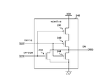
- 3 is a circuit diagram showing a configuration example of a NAND (Negative AND) gate in the first embodiment.
- FIG. 1 is a block diagram illustrating a configuration example of the electronic device 100 according to the first embodiment.
- the electronic device 100 includes a communication interface 110, a clock data recovery circuit 200, and a data processing unit 120.
- the communication interface 110 transmits / receives a data signal to / from an external device (such as a source device).
- the communication interface 110 receives the data signal DATA on which the clock signal is superimposed, and supplies the data signal DATA to the clock data recovery circuit 200 via the signal line 119.
- the communication standard of the communication interface 110 for example, DisplayPort v1.3, MIPI (Mobile Industry Processor Interface) M-PHY v4.0 standard is used.
- the clock data recovery circuit 200 generates a clock signal CK substantially the same as the clock signal superimposed on the data signal DATA from the data signal DATA.
- the clock data recovery circuit 200 internally generates a clock signal CK by an oscillator, and adjusts the phase of the clock signal CK according to the data signal. Thereby, a signal substantially coincident with the clock signal superimposed on the transmission side is reproduced as the clock signal CK.
- the clock data recovery circuit 200 supplies the data signal DATA and the generated clock signal CK to the data processing unit 120 via signal lines 208 and 209.
- the data processing unit 120 captures and processes the data signal DATA in synchronization with the clock signal CK.
- the data processing unit 120 performs, for example, processing for converting serial data into parallel data, audio processing, image processing, and the like.
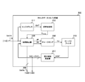
- FIG. 2 is a block diagram illustrating a configuration example of the clock data recovery circuit 200 according to the first embodiment.
- the clock data recovery circuit 200 includes an edge counter 211, a switching control unit 212, a phase detector 220, a charge pump 250, a low pass filter 213, and a voltage controlled oscillator 214.
- the edge counter 211 counts the number of rising edges and falling edges (eg, rising edges) of the data signal DATA.
- the edge counter 211 supplies the count value to the switching control unit 212 as the counter value CNT.
- the edge counter 211 resets the count value to the initial value and performs counting.
- the switching control unit 212 generates a switching control signal D change based on the counter value CNT and supplies it to the phase detector 220.
- the switching control signal D change is a signal that designates one of the rising edge and the falling edge of the data signal DATA as a designated edge. For example, when the rising edge is designated, the switching control signal D change is set to a high level, and when the falling edge is designated, the switching control signal D change is set to a low level.
- the state in which the phase detector 220 detects the phase difference in accordance with the switching control signal D change that specifies the rising edge is referred to as a “rising edge detection mode”.
- the state in which the phase detector 220 detects the phase difference according to the switching control signal D change that designates the falling edge is referred to as a “falling edge detection mode”.
- the switching control unit 212 switches the detection mode by inverting the switching control signal D change every time a certain number of edges are counted by the edge counter 211.
- the switching control unit 212 switches the detection mode by inverting the switching control signal D change every time a certain number of edges are counted
- the present invention is not limited to this configuration.
- the switching control unit 212 may switch the detection mode every time a predetermined time elapses.
- the phase detector 220 detects a phase difference between a designated edge indicated by the switching control signal D change and a specific edge (for example, a falling edge) among the rising edge and the falling edge of the clock signal CK.
- the phase detector 220 generates detection signals UP and DN based on the detection result.
- the difference between the low level periods of the detection signals UP and DN indicates the phase difference between the designated edge of the data signal DATA and the falling edge of the clock signal CK.
- the phase detector 220 supplies detection signals UP and DN to the charge pump 250. Further, the phase detector 220 supplies the data signal DATA to the data processing unit 120.
- the charge pump 250 converts the detection signals UP and DN from the phase detector 220 into a current signal I cp having a current value corresponding to the phase difference.
- the charge pump 250 supplies the current signal I cp to the low pass filter 213.
- the low-pass filter 213 converts a component of the current signal I cp having a frequency equal to or lower than a predetermined cutoff frequency into a voltage signal VCNT having a voltage value corresponding to the phase difference.
- the low-pass filter 213 is an analog filter composed of, for example, a resistor or a capacitor.
- the low pass filter 213 supplies the generated voltage signal VCNT to the voltage controlled oscillator 214.
- the voltage controlled oscillator 214 generates a clock signal CK having a frequency corresponding to the phase difference indicated by the voltage signal VCNT. For example, the longer the low level period of the detection signal UP with respect to the detection signal DN, the higher the voltage signal VCNT, and the higher the frequency of the clock signal CK is controlled. On the other hand, the longer the low level period of the detection signal DN with respect to the detection signal UP, the lower the voltage signal VCNT and the lower the frequency of the clock signal CK is controlled.
- the voltage controlled oscillator 214 supplies the generated clock signal CK to the phase detector 220 and the data processing unit 120.
- the voltage controlled oscillator 214 is an example of an oscillator described in the claims.
- the frequency of the clock signal CK is controlled to a value corresponding to the phase difference between the data signal DATA and the clock signal CK by the phase detector 220, the charge pump 250, the low pass filter 213, and the voltage control oscillator 214.
- the phase of the clock signal CK is stabilized at a value synchronized with the data signal DATA (in other words, locked). Thereby, the clock signal superimposed on the data signal DATA is reproduced.
- the present invention is not limited to this configuration. These circuits may be provided in a phase synchronization circuit that synchronizes two clock signals. In this case, two clock signals are input to the phase detector 220 instead of the data signal DATA and the clock signal CK.
- the phase detector 220 generates the clock signal CK internally, but may generate a periodic signal other than the clock signal, such as a strobe signal.
- the circuit in the clock data recovery circuit 200 is an example of a phase synchronization circuit described in the claims.
- the data signal DATA is an example of an input signal recited in the claims
- the clock signal CK is an example of a periodic signal recited in the claims.
- FIG. 3 is a diagram illustrating an example of the operation of the switching control unit 212 in the first embodiment.
- the switching control unit 212 inverts the switching control signal D change .
- the counter value CNT is not the value (3n)
- the value of the switching control signal D change is held.
- n is an integer.
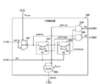
- FIG. 4 is a circuit diagram illustrating a configuration example of the phase detector 220 according to the first embodiment.
- This phase detector 220 includes selectors 221 and 298, a front-stage flip-flop 222, a rear-stage flip-flop 223, and NAND gates 230 and 224.
- selectors 221 and 298, a front-stage flip-flop 222, a rear-stage flip-flop 223, and NAND gates 230 and 224 As the front-stage flip-flop 222 and the rear-stage flip-flop 223, for example, D-type flip-flops are used.
- the selector 221 selects either the data signal DATA or an inverted signal obtained by inverting the data signal DATA in accordance with the switching control signal D change .
- the selector 221 selects the data signal DATA when the switching control signal D change is at a high level (rising edge detection mode), and is inverted when the switching control signal D change is at a low level (falling edge detection mode). Select a signal. Then, the selector 221 supplies the selected signal to the NAND gate 224 and the previous flip-flop 222 as the internal signal sDATA.
- the selector 221 is an example of a selection unit described in the claims.
- the pre-stage flip-flop 222 holds the internal signal sDATA from the selector 221 in synchronization with the clock signal CK.
- the front-stage flip-flop 222 supplies the held signal as the internal signal DFF1Q to the selector 298, the NAND gate 230, and the rear-stage flip-flop 223.
- the front-stage flip-flop 222 supplies the inverted signal of the held signal to the NAND gate 224 as the internal signal DFF1QB.
- the post-stage flip-flop 223 holds the internal signal DFF1Q from the pre-stage flip-flop 222 in synchronization with a signal obtained by inverting the clock signal CK.
- the subsequent flip-flop 223 supplies the inverted signal of the held signal to the NAND gate 230 as the internal signal DFF2QB.
- the NAND gate 230 outputs a negative logical product of the internal signal DFF1Q and the internal signal DFF2QB to the charge pump 250 as a detection signal DN.
- the NAND gate 230 is an example of a first NAND gate described in the claims.
- the NAND gate 224 outputs a negative logical product of the internal signal sDATA and the internal signal DFF1QB as a detection signal UP to the charge pump 250.
- the NAND gate 224 is an example of a second NAND gate described in the claims.
- These detection signals UP and DN indicate a phase difference between the rising edge of the internal signal sDATA from the selector 221 and the falling edge of the clock signal CK. Therefore, when the selector 221 selects the data signal DATA as the internal signal sDATA, the phase difference between the “rising edge” of the data signal DATA and the falling edge of the clock signal CK is detected. On the other hand, when the selector 221 selects the inverted signal of the data signal DATA as the internal signal sDATA, the phase difference between the “falling edge” of the data signal DATA and the falling edge of the clock signal CK is detected. . As described above, the selector 221 switches between the data signal DATA and its inverted signal, whereby the edge (designated edge) for detecting the phase difference can be switched in the data signal DATA.
- the selector 298, in accordance with the switching control signal D change, and selects the internal signal DFF1Q, one of an inverted signal obtained by inverting the internal signal DFF1Q.
- the configuration of the selector 298 is the same as that of the selector 221.
- the selector 298 supplies the selected signal to the data processing unit 120 as the recovered new data signal DATA.
- the selector 298 may use the internal signal from the output terminal Q of the subsequent flip-flop 223 instead of the internal signal DFF1Q from the previous flip-flop 222. In this case, the selector 298 selects either the internal signal from the subsequent flip-flop 223 or its inverted signal according to the switching control signal D change .
- a circuit including the selector 221, the NAND gate 230, and the NAND gate 224 is an example of a detection unit described in the claims.
- a circuit including the front-stage flip-flop 222 and the rear-stage flip-flop 223 is an example of a holding unit described in the claims.
- the phase detector 220 detects the phase difference between the specified edge of the data signal DATA and the falling edge of the clock signal CK, but the phase difference between the specified edge of the data signal DATA and the rising edge of the clock signal CK. May be detected.
- the front-stage flip-flop 222 may operate in synchronization with the inverted signal of the clock signal CK, and the rear-stage flip-flop 223 may operate in synchronization with the clock signal CK.
- Such a phase detector 220 is used, for example, in a phase synchronization circuit that detects a phase difference between two clock signals.
- FIG. 5 is a circuit diagram showing a configuration example of the NAND gate 230 in the first embodiment.
- the NAND gate 230 includes P-type MOS (metal-oxide-semiconductor) transistors 231 and 232 and N-type MOS transistors 233 and 234.
- P-type MOS metal-oxide-semiconductor
- the internal signal DFF 1 Q is input to the gate of the P-type MOS transistor 231, and the internal signal DFF 2 QB is input to the gate of the P-type MOS transistor 232.
- P-type MOS transistors 231 and 232 are inserted in parallel between the power supply and the output terminal of NAND gate 230.
- the internal signal DFF1Q is input to the gate of the N-type MOS transistor 233, and the internal signal DFF2QB is input to the gate of the N-type MOS transistor 234.
- N-type MOS transistors 233 and 234 are inserted in series between the ground terminal and the output terminal of NAND gate 230.
- the NAND gate 230 outputs a negative logical product of the internal signals DFF1Q and DFF2QB.
- the structure of the NAND gate 224 is the same as that of the NAND gate 230.
- the delay times of the NAND gate 230 shown in FIG. 5 and a NOR gate described later with reference to FIG. 14 will be considered.
- the drain current of the P-type MOS transistor is smaller than that of the N-type MOS transistor.
- the drain current of a P-type MOS transistor is half that of an N-type MOS transistor of the same size.
- the transistors of the P-type MOS transistor connected in parallel and the N-type MOS transistor connected in series have the same drain current.
- the size is set. Under the premise that the drain current of the P-type MOS transistor is half that of the N-type MOS transistor, the balance between the drain currents of FIG. 5 is obtained by using a P-type MOS transistor (231 etc.) and an N-type MOS transistor (233 etc.). What is necessary is just to make each size the same. This size is, for example, 2u.
- the size of the N-type MOS transistor is 4u and the size of the P-type MOS transistor is 1u. And it is sufficient.
- the larger the transistor size the larger the gate capacitance and the longer the time required for charging / discharging (that is, the delay time). Therefore, the larger NOR gate has a longer delay time than the NAND gate.
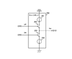
- FIG. 6 is a circuit diagram showing a configuration example of the charge pump 250 according to the first embodiment.
- the charge pump 250 includes constant current sources 251 and 254 and switches 252 and 253.
- the constant current sources 251 and 254 supply a constant current.
- Switches 252 and 253 are inserted in series between current sources 251 and 254.
- the constant current source 251 and the switch 252 are disposed on the power supply side, and the constant current source 254 and the switch 253 are disposed on the ground side.
- the connection point between the switches 252 and 253 is connected to the low-pass filter 213.
- the switch 252 opens and closes the line according to the detection signal UP, and the switch 253 opens and closes the line according to the detection signal DN. For example, the switch 252 shifts to an open state when the detection signal UP is at a low level, and the switch 253 shifts to an open state when the detection signal is at a low level.
- the current signal I cp corresponding to the difference (phase difference) between the low level periods of the detection signal UP and the detection signal DN is generated.
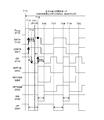
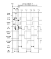
- FIG. 7 is a timing chart showing an example of the operation of the phase detector 220 in the rising edge detection mode in the first embodiment.
- the selector 221 selects the data signal DATA and outputs it as the internal signal sDATA.
- a data signal DATA having a periodic pattern such as “1010...” In binary notation is input.
- the signal of this pattern is stored in a preamble signal or the like transmitted prior to data to be transmitted, and is used for phase synchronization.
- the post-stage flip-flop 223 holds the internal signal DFF1Q in synchronization with the falling edge of the clock signal (timing T16, etc.), inverts the hold value, and outputs it as the internal signal DFF2QB.
- the NAND gate 224 outputs a negative logical product of the internal signal sDATA and DFF1QB as the detection signal UP.
- the detection signal DN falls.
- the detection signal UP rises.
- the NAND gate 230 outputs a negative logical product of the internal signals DFF1Q and DFF2QB as the detection signal DN.
- the detection signal DN falls. Further, the detection signal DN rises when the pulse width of the clock signal CK elapses after the clock signal CK rises (timing T16 or the like).
- the frequency of the clock signal CK is controlled so that the difference (phase difference) between the low levels of the detection signals UP and DN is reduced. As a result, the phase of the falling edge of the clock signal CK is locked to the timing of the rising edge of the data signal DATA (such as T12).
- the phase of the rising edge of the clock signal CK is locked at a position (such as T14) 0.5 UI (Unit Interval) from the rising edge of the data signal DATA.
- the UI is a time for transferring one bit, and is 50 picoseconds (ps) when the transfer rate of the data signal DATA is 10 Gbps (Giga Bit per second).
- the squares filled with black indicate the phase of the rising edge of the clock signal CK before locking
- the white squares indicate the phase of the rising edge of the clock signal CK after locking.
- FIG. 8 is a timing chart showing an example of the operation of the phase detector 220 in the falling edge detection mode according to the first embodiment. After timing T21 when the switching control signal D change is switched to the low level (falling edge detection mode), the selector 221 selects the inverted signal of the data signal DATA and outputs it as the internal signal sDATA.
- the NAND gate 224 outputs a negative logical product of the internal signal sDATA ( ⁇ DATA) and DFF1QB as the detection signal UP.
- the detection signal UP falls.
- the clock signal CK rises during a period (such as timing T25) in which the internal signal sDATA is at a high level (that is, DATA is at a low level) in which the internal signal sDATA is at a high level (that is, DATA is at a low level), the detection signal UP rises.
- the NAND gate 230 outputs a negative logical product of the internal signals DFF1Q and DFF2QB as the detection signal DN.
- the detection signal DN falls.
- the detection signal DN rises when the pulse width of the clock signal CK elapses after the clock signal CK rises (timing T26, etc.).
- the frequency of the clock signal CK is controlled so that the difference (phase difference) between the low levels of the detection signals UP and DN is reduced.
- the phase of the falling edge of the clock signal CK is locked to the timing of the falling edge of the data signal DATA (T22, etc.).
- the phase of the rising edge of the clock signal CK is locked at a position (such as T24) of 0.5 UI from the rising edge of the data signal DATA.
- the triangles filled in with black indicate the phase of the rising edge of the clock signal CK before locking
- the white triangles indicate the phase of the rising edge of the clock signal CK after locking.
- the NAND gate 230 and the like operate on either the rising edge or the falling edge of the data signal DATA.
- the XOR gate operates on both the rising edge and falling edge of the data signal DATA. For this reason, by providing the NAND gate 230 and the like, the power consumption of the phase detector 220 can be reduced as compared with the case where the XOR gate is provided.
- FIG. 9 is a timing chart showing an example of operations of the edge counter 211 and the switching control unit 212 in the first embodiment.
- the edge counter 211 counts up the counter value CNT in synchronization with the rising edge of the data signal DATA.
- the switching control unit 212 Inverts the switching control signal D change of the initial value (low level or the like). Thereby, the detection mode is switched. Further, at timing T32 when the counter value CNT becomes 6, the switching control unit 212 inverts the switching control signal D change again. Thus, the detection mode is switched every time a certain number of edges are counted.
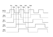
- FIG. 10 is a diagram for explaining a phase lock position in the first embodiment.
- the phase difference between the rising edge (such as T42) of the data signal and the falling edge (such as T41) of the clock signal CK is detected.
- the phase of the rising edge of the clock signal CK is adjusted to 0.5 UI (such as timing T45) from the rising edge of the data signal DATA.
- the phase difference between the falling edge of the data signal (such as T47) and the falling edge of the clock signal CK is detected.
- the phase of the rising edge of the clock signal CK is adjusted to 0.5 UI (such as timing T43) from the falling edge of the data signal DATA.
- the switching control unit 212 alternately switches between the rising edge detection mode and the falling edge detection mode, so that the rising phase of the clock signal CK is at the timing (T44) between the timings T43 and T45 described above. Locked.
- the rising edge of the clock signal CK is locked at a timing T45 of 0.5 UI from the rising edge of the data signal DATA.
- jitter such as data dependent jitter (DDJ: Data Dependent Jitter) and periodic jitter (PJ: Periodic Jitter) occurs.
- DDJ Data Dependent Jitter
- PJ Periodic Jitter
- This hold time is the minimum time that the flip-flop must keep holding the data signal of the same value after the rising edge of the clock signal.
- the hold time margin decreases, the data signal changes before the hold time elapses, and there is a high possibility that a hold time error will occur in the preceding flip-flop 222.
- the setup time margin is reduced. This setup time is the minimum time that the data signal having the same value must be continuously input to the flip-flop prior to the rise of the clock signal.
- the setup time margin is reduced, the clock signal CK rises before the setup time elapses, and there is a high possibility that a setup time error will occur in the preceding flip-flop 222.
- the phase detector 220 locks the phase of the clock signal CK around the middle of the rising edge and falling edge of the data signal DATA (such as T44) in order to detect the phase difference by switching the detection mode. Can do.
- the setup time and hold time margins increase and the rate of occurrence of setup time errors and hold time errors decreases as compared with the case where the detection mode is not switched. That is, even if there is jitter, an error hardly occurs and jitter tolerance can be improved.
- FIG. 11 is a graph showing an example of the relationship between the input phase difference and the output phase difference in the first embodiment.
- the horizontal axis in the figure indicates the phase difference between the data signal DATA and the clock signal CK as the input phase difference.
- the vertical axis indicates the phase difference between the detection signal UP and the detection signal DN as an output phase difference.
- a indicates the characteristics of the phase detector 220 provided with NAND gates 230 and 224.
- phase difference detection when an input phase difference signal in the range of ⁇ 180 degrees to 180 degrees is input, an output phase difference having the same value is detected in the entire range.
- a part of the phase difference within the range is not detected due to the delay time of the NAND gates 230 and 224.
- P in_max when there is no jitter and the input phase difference is larger than a certain value P in_max , the low level period of the detection signal UP becomes shorter than the delay time of the NAND gate 230.
- the phase difference cannot be detected.
- the hatched portion indicates a range where phase difference cannot be detected.
- phase difference detection cannot be performed in a range larger than P in_max '.
- FIG. 11 shows the characteristics of a Hodge type phase detector that detects a phase difference with a NOR gate without switching the detection mode. Similarly, in this phase detector, no phase difference is detected in the shaded area. However, the range in which the phase difference cannot be detected is larger than a in FIG. This is because the delay time of the NOR gate becomes longer than that of the NAND gate as described in FIG.
- the range in which the phase difference can be detected can be widened as compared with the case of using the NOR gate.
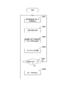
- FIG. 12 is a flowchart illustrating an example of the operation of the clock data recovery circuit 200 according to the first embodiment. This operation is started when the data signal DATA is input from the communication interface 110, for example.
- the phase detector 220 in the clock data recovery circuit 200 detects the phase difference between the data signal DATA and the clock signal CK according to the switching control signal D change (step S901).
- the low pass filter 213 generates a voltage signal VCNT corresponding to the detected phase difference (step S902).
- the voltage controlled oscillator 214 generates a clock signal CK having a frequency corresponding to the phase difference indicated by the voltage control signal VCNT (step S903).
- the edge counter 211 counts rising edges of the data signal DATA (Step S904).
- the switching control unit 212 determines whether or not the rising edge count value (CNT) is 3n (step S905). When the count value is 3n (step S905: Yes), the switching control unit 212 switches the detection mode by inverting the switching control signal D change (step S906). On the other hand, when the count value is not 3n (step S905: No), or after step S906, the clock data recovery circuit 200 repeats step S901 and subsequent steps.
- CNT rising edge count value
- the phase detector 220 detects the phase difference between the edge of the data signal specified by the switching control signal and the falling edge of the clock signal.
- the phase difference can be detected by switching the edge of the data signal to be detected.
- the rising edge of the clock signal can be locked near the middle between the rising edge and the falling edge of the data signal. Therefore, it is possible to suppress the occurrence of a setup time error and a hold time error in the preceding flip-flop 222 due to jitter.
- the jitter tolerance of the phase detector 220 can be improved compared to the case where the detection target edge is not switched.
- the phase detector 220 generates the detection signals UP and DN indicating the phase difference based on the difference in the low level period, and the charge pump 250 uses the current signal I cp corresponding to the difference.
- the phase detector 220 is suitable for the charge pump 250. It is necessary to generate the detection signals UP and DN.
- the phase detector 220 according to the second embodiment is different from the first embodiment in that detection signals UP and DN indicating a phase difference are generated by a difference in pulse width.
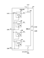
- FIG. 13 is a circuit diagram showing a configuration example of the phase detector 220 according to the second embodiment.
- the phase detector 220 according to the second embodiment is different from the first embodiment in that NOR gates 240 and 225 are provided instead of the NAND gates 230 and 224.
- the NOR gate 240 outputs a negative logical sum of the internal signal DFF1Q from the front-stage flip-flop 222 and the internal signal DFF2QB from the rear-stage flip-flop 223 as the detection signal DN.
- the NOR gate 240 is an example of a first negative OR gate described in the claims.
- the NOR gate 225 outputs a negative OR of the internal signal sDATA from the selector 221 and the internal signal DFF1QB from the previous flip-flop 222 as a detection signal UP.
- the NOR gate 225 is an example of a second NOR gate described in the claims.
- the difference between the pulse widths of the detection signals UP and DN indicates the phase difference between the rising edge of the internal signal sDATA and the falling edge of the clock signal CK.
- a circuit other than the selector 221 in the phase detector 220 that is, a circuit including the front-stage flip-flop 222, the rear-stage flip-flop 223, the NOR gate 240, and the NOR gate 225 has the same configuration as the Hodge type phase detector.
- FIG. 14 is a circuit diagram showing a configuration example of the NOR gate 240 in the second embodiment.
- This NOR gate 240 includes P-type MOS transistors 241 and 242 and N-type MOS transistors 243 and 244.
- the internal signal DFF2QB is input to the gate of the P-type MOS transistor 241, and the internal signal DFF1Q is input to the gate of the P-type MOS transistor 242.
- P-type MOS transistors 241 and 242 are inserted in series between the power supply and the output terminal of NOR gate 240.
- the internal signal DFF2QB is input to the gate of the N-type MOS transistor 243, and the internal signal DFF1Q is input to the gate of the N-type MOS transistor 244.
- N-type MOS transistors 243 and 244 are inserted in parallel between the ground terminal and the output terminal of NOR gate 240.
- the NOR gate 240 outputs a negative logical sum of the internal signals DFF1Q and DFF2QB.
- the structure of the NOR gate 225 is the same as that of the NOR gate 240.
- the phase detector 220 of the second embodiment the switching detection signal D change to the low level is set at the time of the rising edge detection mode, switching detection signal D change to a high level during the falling edge detection mode Is set.
- the selector 221 selects a signal obtained by inverting the data signal DATA in the rising edge detection mode, and selects the data signal DATA in the falling edge detection mode.
- charge pump 250 of the second embodiment has the same configuration as that of the first embodiment.
- the switch 252 shifts to a closed state
- the switch 253 shifts to a closed state
- the low-pass filter 213 generates a current signal I cp corresponding to the difference (phase difference) between the pulse widths of the detection signals UP and DN.
- FIG. 15 is a timing chart showing an example of the operation of the phase detector 220 in the rising edge detection mode according to the second embodiment.
- the selector 221 selects the inverted signal of the data signal DATA and outputs it as the internal signal sDATA.
- the NOR gate 225 outputs a negative logical sum of the internal signal sDATA and the internal signal DFF1QB as the detection signal UP.
- the detection signal UP rises.
- the clock signal CK rises within a period during which the internal signal sDATA is at a low level (timing T55, etc.)
- the detection signal UP falls.
- the NOR gate 240 outputs a negative logical sum of the internal signal DFF1Q and the internal signal DFF2QB as the detection signal DN.
- the detection signal DN rises.
- the detection signal DN falls when the pulse width of the clock signal CK elapses after the rise of the clock signal CK (timing T56, etc.).
- the frequency of the clock signal CK is controlled so that the difference (phase difference) between the pulse widths of the detection signals UP and DN is reduced. As a result, the phase of the rising edge of the clock signal CK is locked at a position of 0.5 UI (such as timing T54) from the timing of the rising edge of the data signal DATA.
- FIG. 16 is a timing chart showing an example of the operation of the phase detector 220 in the falling edge detection mode according to the second embodiment.
- the selector 221 selects the data signal DATA and outputs it as the internal signal sDATA.
- the NOR gate 225 outputs a negative logical sum of the internal signal sDATA and the internal signal DFF1QB as the detection signal UP.
- the detection signal UP rises.
- the clock signal CK rises within a period during which the internal signal sDATA is at a low level (timing T65 or the like), the detection signal UP falls.
- the NOR gate 240 outputs a negative logical sum of the internal signal DFF1Q and the internal signal DFF2QB as the detection signal DN.
- the detection signal DN rises.
- the detection signal DN falls when the pulse width of the clock signal CK elapses after the clock signal CK rises (timing T66, etc.).
- the frequency of the clock signal CK is controlled so that the difference (phase difference) between the pulse widths of the detection signals UP and DN is reduced. Thereby, the phase of the rising edge of the clock signal CK is locked at a position of 0.5 UI (such as T64) from the timing of the falling edge of the data signal DATA.
- the phase detector 220 detects the phase difference by the NOR gate 240 or the like, and therefore detects the detection signals UP and DN indicating the phase difference by the difference in pulse width. Can be generated.
- the phase can be controlled in the clock data recovery circuit 200 provided with the charge pump 250 that generates a current signal corresponding to the difference between the pulse widths of the detection signals UP and DN.
- circuits other than the selector 221 are operated in common in both the rising edge detection mode and the falling edge detection mode. However, if the circuit that operates only in the rising edge detection mode and the circuit that operates only in the falling edge detection mode are provided separately, the operation time per circuit is halved, and the life of the semiconductor elements in the circuit is reduced. Can be long.
- the phase detector 220 of the third embodiment is different from the first embodiment in that a circuit is provided for each detection mode.
- FIG. 17 is a circuit diagram showing a configuration example of the phase detector 220 according to the third embodiment.
- the phase detector 220 of the third embodiment is different from that of the first embodiment in that the selector 221 is not provided, and NOR gates 240 and 225, inverters 226 and 228, and buffers 227 and 229 are further provided. Different. Further, a buffer 299 is provided instead of the selector 221.
- the NAND gates 230 and 224 of the third embodiment further include an enable terminal, and the switching control signal D change is input to the enable terminal.
- the NOR gates 240 and 225 of the third embodiment also include an enable terminal, and a signal obtained by inverting the switching control signal D change is input to the enable terminal.
- the NAND gate 230 supplies a negative logical sum of the input values to the inverter 226 and the buffer 227 when the switching control signal D change is at a high level (rising edge detection mode).
- the NAND gate 224 also supplies a negative logical sum of the input values to the inverter 228 and the buffer 229 when the switching control signal D change is at a high level.
- the switching control signal Dchange is at a low level, the output terminals of the NAND gates 230 and 224 are in a high impedance state.
- the NOR gate 240 supplies a negative logical sum of the input values to the inverter 226 and the buffer 227 when the switching control signal D change is at a low level (falling edge detection mode).
- the NOR gate 225 also supplies a negative logical sum of the input values to the inverter 228 and the buffer 229 when the switching control signal D change is at a low level.
- the switching control signal Dchange is at a high level, the output terminals of the NOR gates 240 and 225 are in a high impedance state.
- the inverters 226 and 228 invert the input signal according to the switching control signal D change and output it.
- Inverter 226 inverts the input signal and outputs it as detection signal DN when switching control signal D change is at the high level (rising edge detection mode).
- the inverter 228 also inverts the input signal and outputs it as the detection signal UP when the switching control signal D change is at a high level.
- the switching control signal Dchange is at a low level, the output terminals of the inverters 226 and 228 are in a high impedance state.
- the buffers 227 and 229 output the input signal with a delay in accordance with the switching control signal D change .
- the delay times of these buffers 227 and 229 are adjusted to the same extent as inverters 226 and 228.
- the buffer 227 delays the input signal and outputs it as a detection signal DN when the switching control signal D change is at a low level (falling edge detection mode).
- the buffer 229 also delays the input signal and outputs it as the detection signal UP when the switching control signal D change is at a low level.
- the switching control signal Dchange is at a high level, the output terminals of the buffers 227 and 229 are in a high impedance state.
- the buffer 299 buffers the internal signal DFF1Q and supplies it to the data processing unit 120 as the recovered data signal DATA.
- the buffer 299 may use an internal signal from the output terminal Q of the rear-stage flip-flop 223 instead of the internal signal DFF1Q from the front-stage flip-flop 222.
- the charge pump 250 at the subsequent stage generates a current signal I cp corresponding to the difference between the pulse widths of the detection signals UP and DN, as in the second embodiment.
- the circuit composed of the NAND gate 230, the NAND gate 224, the inverter 226, and the inverter 228 operating in the rising edge detection mode is an example of the rising edge detection circuit in the claims.
- the circuit composed of the NOR gate 240, the NOR gate 225, the buffer 227, and the buffer 229 that operates in the falling edge detection mode is an example of the falling edge detection circuit in the claims.
- the circuit that operates in the rising edge detection mode and the circuit that operates in the falling edge detection mode are provided separately, and thus operate in common in those modes.
- the operation time of each circuit can be reduced as compared with a configuration in which a circuit is provided. Thereby, the lifetime of the semiconductor element in a circuit can be lengthened.
- the switching control signal D change is input to the enable terminal to switch between the circuit operating in the rising edge detection mode and the circuit operating in the falling edge detection mode.
- the selector may be operated by switching between a circuit operating in the rising edge detection mode and a circuit operating in the falling edge detection mode.
- the phase detector 220 in the modification of the third embodiment is different from the third embodiment in that a selector is further provided.
- FIG. 18 is a circuit diagram showing a configuration example of the phase detector 220 in a modification of the third embodiment.
- the phase detector 220 of this modification is different from the third embodiment in that it further includes selectors 261, 262, 263, 264, 265, and 266.
- the selectors 261, 262, 263, and 264 select one of the two output destinations according to the switching control signal D change and output an input signal to the output destination.
- the selector 261 outputs the internal signal DFF1Q to the NAND gate 230 when the switching control signal D change is at a high level (rising edge detection mode).
- the selector 261 when the switching control signal D change is at the low level, the selector 261 outputs the internal signal DFF1Q to the NOR gate 240.
- the selector 262 outputs the internal signal DFF2QB to the NAND gate 230 when the switching control signal D change is at a high level, and outputs the internal signal DFF2QB to the NOR gate 240 when the switching control signal D change is at a low level.
- the selector 263 outputs the data signal DATA to the NAND gate 224 when the switching control signal D change is at the high level, and outputs the data signal DATA to the NOR gate 225 when the switching control signal D change is at the low level. To do.
- the selector 264 outputs the internal signal DFF1QB to the NAND gate 224 when the switching control signal D change is at a high level, and outputs the internal signal DFF1QB to the NOR gate 225 when the switching control signal D change is at a low level.
- the NAND gate 230 of the modified example outputs a negative logical product only to the inverter 226, and the NAND gate 224 outputs a negative logical product only to the inverter 228.
- the NOR gate 240 outputs a negative logical sum only to the buffer 227, and the NOR gate 225 outputs a negative logical sum only to the buffer 229.
- the selectors 265 and 266 select and output one of the two input signals according to the switching control signal D change .
- the selector 265 selects the signal from the inverter 226 and outputs it as the detection signal DN when the switching control signal D change is at a high level.
- the selector 265 selects the signal from the buffer 227 when the switching control signal D change is at a low level.
- the selector 266 selects the signal from the inverter 228 and outputs it as the detection signal UP when the switching control signal D change is at a high level.
- the selector 266 selects the signal from the buffer 229 when the switching control signal D change is at a low level.
- the outputs (UP and DN) of the phase detector 220 may become unstable immediately after switching the detection mode.
- the charge pump 250 controls the frequency based on the unstable output, there is a problem that the frequency is not controlled appropriately.
- the clock data recovery circuit 200 according to the fourth embodiment is different from the first embodiment in that a malfunction immediately after switching of the detection mode is suppressed.
- FIG. 19 is a block diagram illustrating a configuration example of the clock data recovery circuit 200 according to the fourth embodiment.
- the clock data recovery circuit 200 according to the fourth embodiment includes a phase detector 270, an arithmetic circuit 290, and a digital control oscillator 215.
- the arithmetic circuit 290 includes a detection number counter 291, a frequency control unit 292, and a switching control unit 293.
- the phase detector 270 detects the phase difference between the designated edge indicated by the switching control signal Dchange and the falling edge of the clock signal CK and generates digital detection signals UP and DN.
- the detection signal UP indicates whether or not the falling edge of the clock signal CK is advanced with respect to the specified edge of the data signal DATA. For example, the high level is set to the detection signal UP when the falling edge of the clock signal CK is advanced, and the low level is set when it is delayed.
- the detection signal DN indicates whether or not the falling edge of the clock signal CK is delayed with respect to the specified edge of the data signal DATA. For example, when the falling edge of the clock signal CK is delayed, the detection signal DN is set to a high level, and when the clock signal CK is advanced, the low level is set.
- the detection number counter 291 counts the counter value CNT in synchronization with the detection signal UP and supplies it to the switching control unit 293.
- the configuration of the switching control unit 293 is the same as that of the switching control unit 212 of the first embodiment.
- the switching control unit 293 supplies the switching control signal D change to the frequency control unit 292 and the phase detector 270.
- the detection number counter 291 counts in synchronization with the detection signal UP, but may count in synchronization with the detection signal DN. In addition, the detection number counter 291 may count in synchronization with the logical sum signal of the detection number UP and DN. In this case, an OR gate is provided in the preceding stage of the detection number counter 291.
- the frequency control unit 292 controls the frequency of the clock signal CK to a value corresponding to the phase difference indicated by the detection signals UP and DN by the digital control signal P control .
- the frequency control unit 293 counts the number of times the detection counts UP and DN have become high levels. Then, the frequency control unit 292 increases the frequency of the clock signal CK as the frequency at which the detection signal UP becomes high level is higher than the frequency at which the detection signal DN becomes high level. On the other hand, the frequency control unit 292 lowers the frequency of the clock signal CK as the frequency at which the detection signal DN goes high is higher than the frequency at which the detection signal UP goes high.
- the frequency control unit 292 stops counting the detection signals UP and DN from when the detection mode is switched to when a certain mask period elapses (in other words, masks the detection signal). The length of this mask period is set to a time shorter than the time from the detection mode switching to the next switching. As described above, the frequency control unit 292 controls the frequency based on the detection signal in the period other than the mask period, thereby preventing the malfunction of the clock data recovery circuit 200 due to the unstable detection signal immediately after the switching.
- the digitally controlled oscillator 215 generates a clock signal CK having a frequency corresponding to the phase difference in accordance with the control signal P control from the frequency control unit 292.
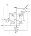
- FIG. 20 is a circuit diagram showing a configuration example of the phase detector 270 in the fourth embodiment.
- the phase detector 270 includes a selector 271, front-stage flip-flops 272 and 273, rear-stage flip-flops 274 and 275, and NOR gates 280 and 276.
- the configuration of the selector 271 is the same as that of the selector 221 of the first embodiment.
- the internal signal sDATA from the selector 261 is supplied to both input terminals of the previous stage flip-flops 272 and 273.
- the pre-stage flip-flop 272 holds the internal signal sDATA in synchronization with the clock signal CK.
- the front-stage flip-flop 272 supplies the held value as the internal signal Q1 to the selector 298, the rear-stage flip-flop 274, and the NOR gate 280.
- the front-stage flip-flop 272 is an example of a first front-stage flip-flop described in the claims.
- the pre-stage flip-flop 273 holds the internal signal sDATA in synchronization with a signal obtained by inverting the clock signal CK.
- the front-stage flip-flop 273 supplies the hold value to the rear-stage flip-flop 275 as the internal signal Q3.
- the front-stage flip-flop 273 is an example of a second front-stage flip-flop described in the claims.
- the post-stage flip-flop 274 holds the internal signal Q1 in synchronization with the clock signal CK.
- the subsequent flip-flop 274 supplies the inverted value of the held value to the NOR gate 276 as the internal signal Q2B.
- the post-stage flip-flop 274 is an example of a first post-stage flip-flop described in the claims.
- the post-stage flip-flop 275 holds the internal signal Q3 in synchronization with the clock signal CK.
- the subsequent flip-flop 275 supplies the retained value as the internal signal Q4 to the NOR gate 276, and supplies the inverted value of the retained value as the internal signal Q4B to the NOR gate 280.
- the post-stage flip-flop 275 is an example of a second post-stage flip-flop described in the claims.
- the NOR gate 280 outputs a negative logical sum of the internal signals Q1 and Q4B as the detection signal DN.
- the NOR gate 280 is an example of a first negative OR gate described in the claims.
- the NOR gate 276 outputs a negative logical sum of the internal signals Q2B and Q4 as the detection signal UP.
- the NOR gate 276 is an example of a second NOR gate described in the claims.
- This phase detector 270 differs from the Hodge type phase detector in that NOR gates (276 and 280) are used instead of the XOR gate, the selector 271 is provided, and the flip-flop is connected to. Since the gate delay of the NOR gate is shorter than that of the XOR gate, the operation speed is improved by using the NOR gate.
- connection destination of the flip-flop in FIG. 20 may be changed as illustrated in FIG. Specifically, the front-stage flip-flop 272 outputs the inverted value of the retained value to the NOR gate 280 as the internal signal Q1B, and the rear-stage flip-flop 274 outputs the retained value to the NOR gate 276 as the internal signal Q2. Further, the post-stage flip-flop 275 outputs the hold value to the NOR gate 280 as the internal signal Q4. Further, the inverting output terminal QB of the post-stage flip-flop 274 and the inverting output terminal QB of the post-stage flip-flop 275 are connected in common to the input terminal of the NOR gate 276.
- FIG. 22 is a timing chart showing an example of the operation of the phase detector 270 in the rising edge detection mode according to the fourth embodiment.
- the selector 271 selects the data signal DATA and outputs it as the internal signal sDATA.
- the NOR gate 276 outputs a negative logical sum of the internal signal Q2B and the internal signal Q4 as the detection signal UP.
- the detection signal UP rises at timing T76 and the like. That is, the detection signal UP indicates whether or not the falling edge of the clock signal CK is delayed with respect to the rising edge of the data signal DATA.
- the NOR gate 280 outputs a negative logical sum of the internal signal Q1 and the internal signal Q4B as the detection signal DN.
- the detection signal DN rises at timing T82 or the like. That is, the detection signal DN indicates whether the falling edge of the clock signal CK is advanced with respect to the rising edge of the data signal DATA.
- the selector 298 selects either the internal signal Q1 or an inverted signal obtained by inverting the internal signal DFF1Q in accordance with the switching control signal D change . Note that the selector 298 may use an internal signal from the output terminal Q of the rear-stage flip-flop 273 instead of the internal signal Q1 from the front-stage flip-flop 272.
- FIG. 23 is a timing chart showing an example of the operation of the phase detector 270 in the falling edge detection mode according to the fourth embodiment.
- the selector 271 selects the inverted signal of the data signal DATA and outputs it as the internal signal sDATA.
- the NOR gate 276 outputs a negative logical sum of the internal signal Q2B and the internal signal Q4 as the detection signal UP.
- the detection signal UP rises at timing T87 and the like.
- the NOR gate 280 outputs a negative logical sum of the internal signal Q1 and the internal signal Q4B as the detection signal DN.
- the detection signal DN rises at timing T93 or the like.
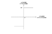
- FIG. 24 is a graph showing an example of the relationship between the input phase difference and the output phase difference in the fourth embodiment.
- the horizontal axis indicates the phase difference (input phase difference) between the data signal DATA and the clock signal CK
- the horizontal axis indicates the phase difference (output phase difference) between the detection signals UP and DN.
- the detection signals UP and DN indicate whether or not the falling edge of the clock signal CK is advanced with respect to the specified edge of the data signal.
- the characteristic that the output value is binary with respect to the input is called a band-band characteristic.
- the arithmetic circuit 290 controls the frequency by masking the detection signal within a certain period from the detection mode switching, the value of the detection signal is immediately after the switching. Even if becomes unstable, the frequency can be controlled appropriately.
- phase difference is detected by the NOR gates 280 and 276.
- these may be replaced by a NAND gate having a relatively short gate delay.
- the phase detector 270 in the modification of the fourth embodiment is different from the fourth embodiment in that a NAND gate is used.
- FIG. 25 is a circuit diagram showing a configuration example of the phase detector 270 in a modification of the fourth embodiment.
- the phase detector 270 according to the modified example is different from the first embodiment in that NAND gates 278 and 279 are provided instead of the NOR gates 280 and 276.
- NAND gate 278 outputs a negative logical product of internal signals Q1 and Q4B as detection signal DN.
- the NAND gate 278 is an example of a first NAND gate described in the claims.
- NAND gate 279 outputs a negative logical product of internal signals Q2B and Q4 as detection signal UP.
- the NAND gate 279 is an example of a second NAND gate described in the claims.
- connection destination of the flip-flop in FIG. 25 may be changed as illustrated in FIG. Specifically, the front-stage flip-flop 272 outputs the inverted value of the retained value to the NAND gate 278 as the internal signal Q1B, and the rear-stage flip-flop 274 outputs the retained value to the NAND gate 279 as the internal signal Q2. Further, the post-stage flip-flop 275 outputs the retained value to the NAND gate 278 as the internal signal Q4. Further, the inverting output terminal QB of the post-stage flip-flop 274 and the inverting output terminal QB of the post-stage flip-flop 275 are connected in common to the input terminal of the NAND gate 279.
- phase difference is detected using the NAND gate 278 or the like having a relatively short gate delay, compared to the case of using the NOR gate, The operation speed of the phase detector 220 can be improved.
- the clock data recovery circuit 200 uses the full rate method of reproducing the clock signal CK having the same clock rate as the data rate of the data signal DATA. However, a half rate method of reproducing the clock signal CK having a clock rate that is half the data rate may be used.
- the clock data recovery circuit 200 according to the fifth embodiment is different from the first embodiment in that the clock signal is recovered by the half rate method.
- FIG. 27 is a block diagram illustrating a configuration example of the clock data recovery circuit 200 according to the fifth embodiment.
- the clock data recovery circuit 200 according to the fifth embodiment includes a voltage controlled oscillator 216 instead of the voltage controlled oscillator 214.
- the voltage controlled oscillator 216 generates clock signals CKI and CKQ and supplies them to the phase detector 220 and the data processing unit 120.
- This clock signal CKQ is a signal whose phase is delayed by ⁇ / 2 with respect to the clock signal CKI.
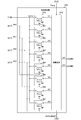
- FIG. 28 is a circuit diagram illustrating a configuration example of the phase detector 200 according to the fifth embodiment.
- the phase detector 220 according to the fifth embodiment is different from the fourth embodiment in that it further includes a front-stage flip-flop 300, a rear-stage 302, and a selector 303.
- the post-stage flip-flop 274 supplies the retained value to the NOR gate 276 and the selector 298 as the internal signal D1d. Further, the post-stage flip-flop 275 supplies the retained value to the selector 303 as the internal signal D2d, and supplies the inverted value of the retained value to the NOR gate 280 as the internal signal D2Bd. Further, a clock signal CKI is supplied to the front-stage flip-flops 272 and 273 and the rear-stage flip-flops 274, 275, and 302.
- the pre-stage flip-flop 301 holds the internal signal sDATA in synchronization with the clock signal CKQ, and supplies the hold value to the post-stage flip-flop 302 as the internal signal D3.
- the post-stage flip-flop 302 holds the internal signal D3 in synchronization with the clock signal CKI, and supplies the hold value to the NOR gate 280 as the internal signal D3d. Further, the post-stage flip-flop 302 supplies the inverted value of the hold value to the NOR gate 276 as the internal signal D3Bd.
- the selector 298 selects either the internal signal D1d or its inverted signal in accordance with the switching control signal D change and outputs it as the data signal DATA_RP.
- the selector 303 selects either the internal signal D2d or its inverted signal in accordance with the switching control signal D change , and outputs it as the data signal DATA_RN.
- phase detector 200 is not limited to the half rate method or the full rate method, and may use a quarter rate method for reproducing the clock signal CK having a clock rate of 1/4 of the data rate, as will be described later.
- FIG. 29 is a timing chart showing an example of the operation of the phase detector 270 in the rising edge detection mode according to the fifth embodiment.
- the NOR gate 276 After timing T91 when the switching control signal D change is switched to the high level (rising edge detection mode), the NOR gate 276 outputs a negative logical sum of the internal signal D1d and the internal signal D3Bd as the detection signal UP. Thereby, the detection signal UP rises at timing T92 and the like.
- the NOR gate 280 outputs a negative logical sum of the internal signal D2Bd and the internal signal D3d as the detection signal UP. Thereby, the detection signal UP rises at timing T93 and the like.
- the phase detector 270 holds the internal signal in synchronization with the clock signals CKI and CKQ. Therefore, the half-rate method is used based on the internal signal. The phase can be detected.
- the detection signals UP and DN are generated by the NOR gates 276 and 280, but other circuits may be used.
- a phase detector 270 according to a modification of the fifth embodiment is different from the fifth embodiment in that the detection signals UP and DN are generated by a circuit other than the NOR gate.
- FIG. 30 is a circuit diagram illustrating a configuration example of the phase detector 270 according to a modification of the fifth embodiment.
- the phase detector 270 of this modification includes flip-flops 304, 305, 306 and 307 and an arithmetic circuit 308.
- the flip-flop 304 holds the data signal DATA in synchronization with the clock signal CKI, and supplies the held value to the arithmetic circuit 308 as the internal signal D1.
- the flip-flop 305 holds the data signal DATA in synchronization with the inverted signal of the clock signal CKI, and supplies the held value to the arithmetic circuit 308 as the internal signal D2.
- the flip-flop 306 holds the data signal DATA in synchronization with the clock signal CKQ, and supplies the held value to the arithmetic circuit 308 as the internal signal D3.
- the flip-flop 307 holds the data signal DATA in synchronization with the inverted signal of the clock signal CKQ, and supplies the held value to the arithmetic circuit 308 as the internal signal D4.
- the arithmetic circuit 308 detects a phase difference based on the internal signals D1 to D4.
- the arithmetic circuit 308 generates detection signals UP and DN from the internal signals D1 and D2 when the switching control signal D change is at a high level (rising edge detection mode). Specifically, the arithmetic circuit 308 monitors the internal signal D1, and when the previous value Q n of the internal signal D1 is different from the current value Q n + 1 , the internal signal D2 is any value of Q n and Q n + 1. Determine if there is.
- the arithmetic circuit 308 detects that the clock signal CKI is leading the rising edge of the data signal DATA, the detection signal of the detection signals UP and a high level of low level DN Is output.
- the arithmetic circuit 308 detects that the clock signal CKI is delayed with respect to the rising edge of the data signal DATA, and detects the high level detection signal UP and the low level.
- the detection signal DN is output.
- the arithmetic circuit 308 generates detection signals UP and DN from the internal signals D3 and D4 when the switching control signal D change is at a low level (falling edge detection mode). Specifically, the arithmetic circuit 308 monitors the internal signal D3, and when the previous value Q n of the internal signal D3 is different from the current value Q n + 1 , the internal signal D4 is at any value of Q n and Q n + 1. Determine if there is. When the internal signal D3 is Q n, the arithmetic circuit 308 detects that the clock signal CKI is advanced with respect to the falling edge of the data signal DATA, the detection signal UP and the high level of the detection signal of the low level DN is output.
- the arithmetic circuit 308 detects that the clock signal CKI is delayed with respect to the falling edge of the data signal DATA, and detects the high level detection signal UP and the low level.
- the detection signal DN is output.
- the arithmetic circuit 308 supplies Q n and Q n + 1 to the data processing unit 120 as recovered data signals.
- FIG. 31 is a timing chart showing an example of the operation of the phase detector 270 in the rising edge detection mode in the modification of the fifth embodiment.
- the arithmetic circuit 308 detects that the clock signal CKI is advanced with respect to the rising edge of the data signal DATA, and outputs the low level detection signal UP and the high level detection signal DN. .
- the phase detector 270 holds the internal signal with the four flip-flops in synchronization with the clock signals CKI and CKQ.
- the phase can be detected by the half rate method based on the signal.
- the clock data recovery circuit 200 uses the full rate method of reproducing the clock signal CK having the same clock rate as the data rate of the data signal DATA. However, a quarter rate method of reproducing the clock signal CK having a clock rate that is 1/4 of the data rate may be used.
- the clock data recovery circuit 200 according to the sixth embodiment is different from the first embodiment in that the clock signal is recovered by the quarter rate method.
- FIG. 32 is a block diagram illustrating a configuration example of the clock data recovery circuit 200 according to the sixth embodiment.
- the clock data recovery circuit 200 according to the sixth embodiment includes a voltage controlled oscillator 217 instead of the voltage controlled oscillator 214.
- the voltage controlled oscillator 218 generates clock signals CK0, CK1, CK2, and CK3 having phases different from each other by ⁇ / 4, and supplies them to the phase detector 220 and the data processing unit 120.
- FIG. 33 is a circuit diagram illustrating a configuration example of the phase detector 270 according to the sixth embodiment.
- the phase detector 270 of the sixth embodiment includes flip-flops 310, 311, 312, 313, 314, 315, 316 and 317 and an arithmetic circuit 318.
- the flip-flop 310 holds the data signal DATA in synchronization with the clock signal CK0, and supplies the held value to the arithmetic circuit 318 as the internal signal D1.
- the flip-flop 311 holds the data signal DATA in synchronization with the clock signal CK1, and supplies the hold value to the arithmetic circuit 318 as the internal signal D2.
- the flip-flop 312 holds the data signal DATA in synchronization with the clock signal CK2, and supplies the held value to the arithmetic circuit 318 as the internal signal D3.
- the flip-flop 313 holds the data signal DATA in synchronization with the clock signal CK3, and supplies the held value to the arithmetic circuit 318 as the internal signal D4.
- the flip-flop 314 holds the data signal DATA in synchronization with the inverted signal of the clock signal CK0, and supplies the held value to the arithmetic circuit 318 as the internal signal D5.
- the flip-flop 315 holds the data signal DATA in synchronization with the inverted signal of the clock signal CK1, and supplies the held value to the arithmetic circuit 318 as the internal signal D6.
- the flip-flop 316 holds the data signal DATA in synchronization with the inverted signal of the clock signal CK2, and supplies the hold value to the arithmetic circuit 318 as the internal signal D7.
- the flip-flop 317 holds the data signal DATA in synchronization with the inverted signal of the clock signal CK3, and supplies the held value to the arithmetic circuit 318 as the internal signal D8.
- the arithmetic circuit 318 detects a phase difference based on the internal signals D1 to D8.
- the arithmetic circuit 318 detects the phase difference from the internal signals D3, D4, and D5 and the phase difference from the internal signals D7, D8, and D1 when the switching control signal D change is at the high level (rising edge detection mode).
- the detection process is alternately performed. Specifically, the arithmetic circuit 318 detects that the clock signal is advanced with respect to the rising edge of the data signal DATA when D3 and D4 are equal and D4 and D5 are different from each other. Detection signal UP and high-level detection signal DN are output.
- the arithmetic circuit 318 detects that the clock signal is delayed with respect to the rising edge of the data signal DATA when D3 and D4 are different from each other, or when D4 and D5 are equal, and detects the high level.
- the signal UP and the low level detection signal DN are output.
- the phase difference is detected by the same method as when D3, D4 and D5 are used. That is, the phase difference is detected based on whether or not a condition that D7 and D8 are equal and D8 and D1 are different is satisfied.
- the arithmetic circuit 318 detects the phase difference from the internal signals D1, D2, and D3 and the internal signals D5, D6, and D7. The process of detecting the phase difference is alternately performed.
- the phase difference is detected by the same method as when the internal signals D3, D4, and D5 are used. The same applies to the case where the internal signals D5, D6, and D7 are used.
- the arithmetic circuit 318 supplies the recovered data signal to the data processing unit 120.
- FIG. 34 is a timing chart for explaining the operation of the phase detector according to the sixth embodiment.
- the internal signal D1 is updated in synchronization with the rising edge of the clock signal CK0
- the internal signal D2 is updated in synchronization with the rising edge of the clock signal CK1.
- the internal signal D3 is updated in synchronization with the rising edge of the clock signal CK2.
- a phase difference is detected from these internal signals D1, D2 and D3 in the falling edge detection mode.
- the internal signal D4 is updated in synchronization with the rising edge of the clock signal CK3 at timing T94, and the internal signal D5 is updated in synchronization with the falling edge of the clock signal CK0 at timing T95.
- a phase difference is detected in the rising edge detection mode from the internal signals D3, D4 and D5.
- the internal signal D6 is updated in synchronization with the falling edge of the clock signal CK1
- the internal signal D7 is updated in synchronization with the falling edge of the clock signal CK2.
- a phase difference is detected in the falling edge detection mode from the internal signals D5, D6 and D7.
- the internal signal D8 is updated in synchronization with the falling edge of the clock signal CK3 at timing T98, and the internal signal D1 is updated in synchronization with the rising edge of the clock signal CK0 at timing T99.
- a phase difference is detected from the internal signals D7, D8 and D1 in the rising edge detection mode.
- the phase detector 270 holds the internal signal in the eight flip-flops in synchronization with the clock signals CK0 to CK3.
- the phase can be detected by the quarter rate method.
- the processing procedure described in the above embodiment may be regarded as a method having a series of these procedures, and a program for causing a computer to execute these series of procedures or a recording medium storing the program. You may catch it.
- a recording medium for example, a CD (Compact Disc), an MD (MiniDisc), a DVD (Digital Versatile Disc), a memory card, a Blu-ray disc (Blu-ray (registered trademark) Disc), or the like can be used.
- this technique can also take the following structures.
- a holding unit that holds an input signal in synchronization with a predetermined periodic signal; Based on the signal held in the holding unit, the phase difference between the specified edge specified by the control signal that specifies one of the rising edge and the falling edge of the input signal as the specified edge and the predetermined periodic signal is detected.
- a phase detector (2)
- the input signal is a data signal;
- the predetermined periodic signal is a clock signal;
- the detection unit includes: A selector that selects either the input signal or an inverted signal obtained by inverting the input signal according to the control signal and supplies the selected signal as an internal signal; A logic circuit that detects a phase difference between one of a rising edge and a falling edge of the internal signal and the predetermined periodic signal based on a signal held in the holding unit;
- the holding part is A pre-stage flip-flop that holds and supplies the internal signal supplied from the selection unit in synchronization with a rising edge of the predetermined periodic signal;
- the phase detector according to (2) further comprising: a rear-stage flip-flop that holds and supplies the internal signal supplied from the front-stage flip-flop in synchronization with a falling edge of the periodic signal.
- the logic circuit is: A first negative AND gate that outputs a negative logical product of the internal signal supplied from the preceding flip-flop and a signal obtained by inverting the internal signal supplied from the subsequent flip-flop; The second negative AND gate that outputs a negative logical product of the internal signal supplied from the selection unit and a signal obtained by inverting the internal signal supplied from the preceding flip-flop. Phase detector.
- the logic circuit includes: A first negative OR gate that outputs a negative OR of the internal signal held in the first front-stage flip-flop and a signal obtained by inverting the internal signal held in the rear-stage flip-flop; The second negative OR gate that outputs a negative logical sum of the internal signal supplied from the selection unit and a signal obtained by inverting the internal signal held in the preceding flip-flop. Phase detector.
- the detection unit includes: A selection unit that selects either the input signal or an inverted signal obtained by inverting the input signal according to the control signal and supplies the selected signal as an internal signal; A logic circuit that detects a phase difference between one of a rising edge and a falling edge of the internal signal and the predetermined periodic signal based on a signal held in the holding unit;
- the holding part is A first front-stage flip-flop that holds and supplies the internal signal supplied from the selection unit in synchronization with a rising edge of the predetermined periodic signal; A first second-stage flip-flop that holds and supplies the internal signal supplied from the first front-stage flip-flop in synchronization with a rising edge of the periodic signal; A second front-stage flip-flop that holds and supplies the internal signal supplied from the selection unit in synchronization with a falling edge of the predetermined periodic signal;
- the phase detector according to (2) further comprising: a second rear-stage flip-flop that holds and supplies the internal signal supplied from the second front-stage flip-flop in synchronization with a rising edge of the periodic
- the logic circuit is: A first NAND gate that outputs a NAND of a signal supplied from the first front-stage flip-flop and a signal supplied from the second rear-stage flip-flop;
- the logic circuit includes: A first negative OR gate that outputs a negative logical sum of the signal supplied from the first front-stage flip-flop and the signal supplied from the second rear-stage flip-flop;
- the phase according to (6) further comprising: a second negative OR gate that outputs a negative OR of the signal supplied from the first latter flip-flop and the signal supplied from the second latter flip-flop.
- Detector (9)
- the detection unit includes: A rising edge detector that detects a phase difference between the rising edge of the input signal and the predetermined periodic signal when the rising edge is specified by the control signal;
- the phase according to (2) further comprising: a falling edge detector that detects a phase difference between the falling edge of the input signal and the predetermined periodic signal when the falling edge is designated by the control signal.
- the input signal is a data signal;
- the predetermined periodic signal is a clock signal;
- (11) The phase detector according to (10), wherein the clock rate is half of the data rate.
- the detection unit includes: A selection unit that selects either the input signal or an inverted signal obtained by inverting the input signal according to the control signal and supplies the selected signal as an internal signal; A logic circuit that detects a phase difference between one of a rising edge and a falling edge of the internal signal and the predetermined periodic signal based on a signal held in the holding unit;
- the holding part is A first front-stage flip-flop that holds and supplies the internal signal supplied from the selection unit in synchronization with a rising edge of the predetermined periodic signal; A first second-stage flip-flop that holds and supplies the internal signal supplied from the first front-stage flip-flop in synchronization with a rising edge of the periodic signal; A second front-stage flip-flop that holds and supplies the internal signal supplied from the selection unit in synchronization with a falling edge of the predetermined periodic signal; A second post-stage flip-flop that holds and supplies the internal signal supplied from the second pre-stage flip-flop in synchronization with a rising edge of the periodic signal; A third front-stage flip-flop that holds and
- the holding portion is A first flip-flop that holds the input signal in synchronization with a rising edge of the predetermined periodic signal and supplies the input signal as an internal signal;
- a second flip-flop that holds the input signal in synchronization with a falling edge of the predetermined periodic signal and supplies the input signal as an internal signal;
- a third flip-flop that holds the input signal in synchronization with a rising edge of a signal having a phase different from that of the predetermined periodic signal by ⁇ / 2, and supplies the input signal as an internal signal;
- a fourth flip-flop that holds the input signal in synchronization with a falling edge of a signal having a phase that is ⁇ / 2 different from that of the predetermined periodic signal and supplies the input signal as an internal signal;
- the detection unit detects the phase difference based on signals from the first, second, third, and fourth flip-flops.
- the predetermined periodic signal includes first, second, third and fourth clock signals having phases different from each other by ⁇ / 4,
- the holding part is A first flip-flop that holds the input signal in synchronization with a rising edge of the first clock signal and supplies the input signal as an internal signal;
- a second flip-flop that holds the input signal in synchronization with a rising edge of the second clock signal and supplies the input signal as an internal signal;
- a fifth flip-flop that holds the input signal in synchronization with a falling edge of the first clock signal and supplies the input signal as an internal signal;
- a sixth flip-flop that holds
- Phase detector (16) a holding unit that holds the input signal in synchronization with a predetermined periodic signal; Based on the signal held in the holding unit, the phase difference between the specified edge specified by the control signal that specifies one of the rising edge and the falling edge of the input signal as the specified edge and the predetermined periodic signal is detected.
- a detector to perform, A phase synchronization circuit comprising: an oscillator that generates the predetermined periodic signal having a frequency corresponding to the phase difference and supplies the signal to the holding unit.
- a switching control unit that switches the designated edge;
- phase difference between the designated edge designated by the control signal that designates one of the rising edge and the falling edge of the input signal as the designated edge and the predetermined periodic signal, and the input signal as the predetermined periodic signal A detection procedure for detecting based on the signal held in the holding unit that holds in synchronization;
- a control method of a phase synchronization circuit comprising: an oscillation procedure that generates the predetermined periodic signal having a frequency corresponding to the phase difference and supplies the signal to the holding unit.
Landscapes
- Physics & Mathematics (AREA)
- Nonlinear Science (AREA)
- Engineering & Computer Science (AREA)
- Computer Networks & Wireless Communication (AREA)
- Signal Processing (AREA)
- Stabilization Of Oscillater, Synchronisation, Frequency Synthesizers (AREA)
- Synchronisation In Digital Transmission Systems (AREA)
- Manipulation Of Pulses (AREA)
Abstract
フリップフロップが設けられた位相検出器の動作レンジを改善し、受信回路のジッタ耐性を向上させる。 位相検出器は、保持部、および、検出部を具備する。位相検出器において、保持部は、入力信号を所定の周期信号に同期して保持する。検出部は、入力信号の立上りエッジおよび立下りエッジの一方を指定エッジとして指定する制御信号により指定された指定エッジと所定の周期信号との位相差を前記保持部に保持された信号に基づいて検出する。
Description
本技術は、位相検出器、位相同期回路、および、位相同期回路の制御方法に関する。詳しくは、フリップフロップが設けられた位相検出器、位相同期回路、および、位相同期回路の制御方法に関する。
従来より、位相同期回路などにおいて、2つの信号の位相差を検出するために位相検出器が用いられている。データ信号およびクロック信号を同期させるアナログの位相同期回路においては、ホッジ型の位相検出器などが用いられる(例えば、非特許文献1参照。)。このホッジ型の位相検出器には、フリップフロップとXOR(排他的論理和)ゲートとが設けられる。フリップフロップは、クロック信号に同期してデータ信号を保持し、XORゲートは、クロックとデータの位相差に応じたパルス信号を出力する。
Behzad Razavi著、「Design of Integrated Circuits for Optical Communications」、(米国)、Wiley、pp294-303.
しかしながら、上述の位相検出器では、XORゲートは、数十ピコ秒(ps)オーダーの狭いパルス幅を出力するのが困難である。その場合、位相検出回路の動作レンジが制限され、受信回路全体のジッタ耐性が低いという問題がある。
本技術はこのような状況に鑑みて生み出されたものであり、フリップフロップが設けられた位相検出器の動作レンジを改善し、受信回路のジッタ耐性を向上させることを目的とする。
本技術は、上述の問題点を解消するためになされたものであり、その第1の側面は、入力信号を所定の周期信号に同期して保持する保持部と、上記入力信号の立上りエッジおよび立下りエッジの一方を指定エッジとして指定する制御信号により指定された上記指定エッジと上記所定の周期信号との位相差を上記保持部に保持された信号に基づいて検出する検出部とを具備する位相検出器である。これにより、入力信号の立上りエッジおよび立下りエッジのうち指定エッジと、周期信号との位相差が検出されるという作用をもたらす。
上記入力信号はデータ信号であり、上記所定の周期信号はクロック信号であり、上記所定の周期信号のクロックレートは、上記入力信号のデータレートと等しくてもよい。これにより、データ信号と、そのデータレートに等しいクロックレートのクロック信号との位相差が検出されるという作用をもたらす。
また、この第1の側面において、上記検出部は、上記入力信号と上記入力信号を反転した反転信号とのいずれかを上記制御信号に従って選択して内部信号として供給する選択部と、上記内部信号の立上りエッジおよび立下りエッジの一方と上記所定の周期信号との位相差を上記保持部に保持された信号に基づいて検出する論理回路とを備え、上記保持部は、上記選択部から供給された上記内部信号を上記所定の周期信号の立上りエッジに同期して保持するとともに供給する前段フリップフロップと、上記前段フリップフロップから供給された上記内部信号を上記周期信号の立下りエッジに同期して保持するとともに供給する後段フリップフロップとを備えてもよい。これにより、入力信号と反転信号とのうち選択された内部信号に基づいて位相差が検出されるという作用をもたらす。
また、この第1の側面において、上記論理回路は、上記前段フリップフロップから供給された上記内部信号と上記後段フリップフロップから供給された上記内部信号を反転した信号との否定論理積を出力する第1の否定論理積ゲートと、上記選択部から供給された上記内部信号と上記前段フリップフロップから供給された上記内部信号を反転した信号との否定論理積を出力する第2の否定論理積ゲートとを備えてもよい。これにより、内部信号の否定論理積が出力されるという作用をもたらす。
また、この第1の側面において、上記論理回路は、上記第1の前段フリップフロップに保持された上記内部信号と上記後段フリップフロップに保持された上記内部信号を反転した信号との否定論理和を出力する第1の否定論理和ゲートと、上記選択部から供給された上記内部信号と上記前段フリップフロップに保持された上記内部信号を反転した信号との否定論理和を出力する第2の否定論理和ゲートとを備えてもよい。これにより、内部信号の否定論理和が出力されるという作用をもたらす。
また、この第1の側面において、上記検出部は、上記入力信号と当該入力信号を反転した反転信号とのいずれかを上記制御信号に従って選択して内部信号として供給する選択部と、上記内部信号の立上りエッジおよび立下りエッジの一方と上記所定の周期信号との位相差を上記保持部に保持された信号に基づいて検出する論理回路とを備え、上記保持部は、上記選択部から供給された上記内部信号を上記所定の周期信号の立上りエッジに同期して保持するとともに供給する第1の前段フリップフロップと、上記第1の前段フリップフロップから供給された上記内部信号を上記周期信号の立上りエッジに同期して保持するとともに供給する第1の後段フリップフロップと、上記選択部から供給された上記内部信号を上記所定の周期信号の立下りエッジに同期して保持するとともに供給する第2の前段フリップフロップと、上記第2の前段フリップフロップから供給された上記内部信号を上記周期信号の立上りエッジに同期して保持するとともに供給する第2の後段フリップフロップとを備えてもよい。これにより、これにより、入力信号と反転信号とのうち選択された内部信号に基づいて位相差が検出されるという作用をもたらす。
また、この第1の側面において、上記論理回路は、上記第1の前段フリップフロップから供給された信号と上記第2の後段フリップフロップから供給された信号との否定論理積を出力する第1の否定論理積ゲートと、上記第1の後段フリップフロップから供給された信号と上記第2の後段フリップフロップから供給された信号との否定論理積を出力する第2の否定論理積ゲートとを備えてもよい。これにより、内部信号の否定論理積が出力されるという作用をもたらす。
また、この第1の側面において、上記論理回路は、上記第1の前段フリップフロップから供給された信号と上記第2の後段フリップフロップから供給された信号との否定論理和を出力する第1の否定論理積ゲートと、上記第1の後段フリップフロップから供給された信号と上記第2の後段フリップフロップから供給された信号との否定論理和を出力する第2の否定論理和ゲートとを備えてもよい。これにより、内部信号の否定論理和が出力されるという作用をもたらす。
また、この第1の側面において、上記検出部は、上記制御信号により上記立上りエッジが指定された場合には上記入力信号の立上りエッジと上記所定の周期信号との位相差を検出する立上りエッジ検出部と、上記制御信号により上記立下りエッジが指定された場合には上記入力信号の立下りエッジと上記所定の周期信号との位相差を検出する立下りエッジ検出部とを備えてもよい。これにより、入力信号の立上りエッジと立下りエッジとが別々の回路で検出されるという作用をもたらす。
また、この第1の側面において、上記入力信号はデータ信号であり、上記所定の周期信号はクロック信号であり、上記所定の周期信号のクロックレートは、上記入力信号のデータレートと異なるものであってもよい。これにより、データ信号と、そのデータレートと異なるクロックレートのクロック信号との位相差が検出されるという作用をもたらす。
また、この第1の側面において、上記クロックレートは、上記データレートの半分であってもよい。これにより、データ信号と、そのデータレートの半分のクロックレートのクロック信号との位相差が検出されるという作用をもたらす。
また、この第1の側面において、上記検出部は、上記入力信号と当該入力信号を反転した反転信号とのいずれかを上記制御信号に従って選択して内部信号として供給する選択部と、上記内部信号の立上りエッジおよび立下りエッジの一方と上記所定の周期信号との位相差を上記保持部に保持された信号に基づいて検出する論理回路とを備え、上記保持部は、上記選択部から供給された上記内部信号を上記所定の周期信号の立上りエッジに同期して保持するとともに供給する第1の前段フリップフロップと、上記第1の前段フリップフロップから供給された上記内部信号を上記周期信号の立上りエッジに同期して保持するとともに供給する第1の後段フリップフロップと、上記選択部から供給された上記内部信号を上記所定の周期信号の立下りエッジに同期して保持するとともに供給する第2の前段フリップフロップと、上記第2の前段フリップフロップから供給された上記内部信号を上記周期信号の立上りエッジに同期して保持するとともに供給する第2の後段フリップフロップと、上記選択部から供給された上記内部信号を、上記所定の周期信号と位相がπ/2異なる信号の立上りエッジに同期して上記内部信号を保持するとともに供給する第3の前段フリップフロップと、上記第3の前段フリップフロップから供給された上記内部信号を上記所定の周期信号の立上りエッジに同期して保持するとともに供給する第3の後段フリップフロップとをさらに備え、上記論理回路は、上記第1の後段フリップフロップから供給された信号と上記第3の後段フリップフロップから供給された信号との否定論理和を出力する第1の否定論理和ゲートと、上記第2の後段フリップフロップから供給された信号と上記第3の後段フリップフロップから供給された信号との否定論理和を出力する第2の否定論理和ゲートとを備えてもよい。これにより、内部信号の否定論理積が出力されるという作用をもたらす。
また、この第1の側面において、上記保持部は、上記入力信号を上記所定の周期信号の立上りエッジに同期して保持するとともに内部信号として供給する第1のフリップフロップと、上記入力信号を上記所定の周期信号の立下りエッジに同期して保持するとともに内部信号として供給する第2のフリップフロップと、上記入力信号を、上記所定の周期信号と位相がπ/2異なる信号の立上りエッジに同期して保持するとともに内部信号として供給する第3のフリップフロップと、上記入力信号を、上記所定の周期信号と位相がπ/2異なる信号の立下りエッジに同期して保持するとともに内部信号として供給する第4のフリップフロップとを備え、上記検出部は、上記第1、第2、第3および第4のフリップフロップからの信号に基づいて上記位相差を検出してもよい。これにより、第1、第2、第3および第4のフリップフロップからの信号に基づいて位相差が検出されるという作用をもたらす。
また、この第1の側面において、上記クロックレートは、上記データレートの1/4であってもよい。これにより、データ信号と、そのデータレートの1/4のクロックレートのクロック信号との位相差が検出されるという作用をもたらす。
また、この第1の側面において、上記所定の周期信号は、互いに位相がπ/4異なる第1、第2、第3および第4のクロック信号を含み、上記保持部は、上記入力信号を上記第1のクロック信号の立上りエッジに同期して保持するとともに内部信号として供給する第1のフリップフロップと、上記入力信号を上記第2のクロック信号の立上りエッジに同期して保持するとともに内部信号として供給する第2のフリップフロップと、上記入力信号を上記第3のクロック信号の立上りエッジに同期して保持するとともに内部信号として供給する第3のフリップフロップと、上記入力信号を上記第4のクロック信号の立上りエッジに同期して保持するとともに内部信号として供給する第4のフリップフロップと、上記入力信号を上記第1のクロック信号の立下りエッジに同期して保持するとともに内部信号として供給する第5のフリップフロップと、上記入力信号を上記第2のクロック信号の立下りエッジに同期して保持するとともに内部信号として供給する第6のフリップフロップと、上記入力信号を上記第3のクロック信号の立下りエッジに同期して保持するとともに内部信号として供給する第7のフリップフロップと、上記入力信号を上記第4のクロック信号の立下りエッジに同期して保持するとともに内部信号として供給する第8のフリップフロップとを備え、上記検出部は、上記第1、第2、第3、第4、第5、第6、第7および第8のフリップフロップからの信号に基づいて上記位相差を検出してもよい。これにより、これにより、第1、第2、第3、第4、第5、第6、第7および第8のフリップフロップからの信号に基づいて位相差が検出されるという作用をもたらす。
また、本技術の第2の側面は、入力信号を所定の周期信号に同期して保持する保持部と、上記入力信号の立上りエッジおよび立下りエッジの一方を指定エッジとして指定する制御信号により指定された上記指定エッジと上記所定の周期信号との位相差を上記保持部に保持された信号に基づいて検出する検出部と、上記位相差に応じた周波数の上記所定の周期信号を生成して上記保持部に供給する発振器とを具備する位相同期回路、および、その制御方法である。これにより、入力信号の立上りエッジおよび立下りエッジのうち指定エッジと、周期信号との位相差が検出されるという作用をもたらす。
また、この第2の側面において、上記指定エッジを切り替える切替制御部と、上記指定エッジが切り替えられたときから一定期間を除く期間において検出された上記位相差に基づいて上記周波数を制御する周波数制御部とをさらに具備してもよい。これにより、指定エッジが切り替えられたときから一定期間を除く期間において検出された上記位相差に基づいて周波数と所定の周期信号の位相が制御されるという作用をもたらす。
本技術によれば、フリップフロップが設けられた位相検出器の動作レンジを改善し、受信回路のジッタ耐性を向上させることができるという優れた効果を奏し得る。なお、ここに記載された効果は必ずしも限定されるものではなく、本開示中に記載されたいずれかの効果であってもよい。
以下、本技術を実施するための形態(以下、実施の形態と称する)について説明する。説明は以下の順序により行う。
1.第1の実施の形態(エッジを切り替えて位相差を検出する例)
2.第2の実施の形態(エッジを切り替えてNORゲートで位相差を検出する例)
3.第3の実施の形態(回路を切り替えて位相差を検出する例)
4.第4の実施の形態(エッジを切り替えて位相差を検出して一定期間内の検出信号をマスクする例)
5.第5の実施の形態(ハーフレート方式でエッジを切り替えて位相差を検出する例)
6.第6の実施の形態(クォーターレート方式でエッジを切り替えて位相差を検出する例)
1.第1の実施の形態(エッジを切り替えて位相差を検出する例)
2.第2の実施の形態(エッジを切り替えてNORゲートで位相差を検出する例)
3.第3の実施の形態(回路を切り替えて位相差を検出する例)
4.第4の実施の形態(エッジを切り替えて位相差を検出して一定期間内の検出信号をマスクする例)
5.第5の実施の形態(ハーフレート方式でエッジを切り替えて位相差を検出する例)
6.第6の実施の形態(クォーターレート方式でエッジを切り替えて位相差を検出する例)
<1.第1の実施の形態>
[電子装置の構成例]
図1は、第1の実施の形態における電子装置100の一構成例を示すブロック図である。この電子装置100は、通信インターフェース110、クロックデータリカバリ回路200およびデータ処理部120を備える。
[電子装置の構成例]
図1は、第1の実施の形態における電子装置100の一構成例を示すブロック図である。この電子装置100は、通信インターフェース110、クロックデータリカバリ回路200およびデータ処理部120を備える。
通信インターフェース110は、外部の装置(ソース機器など)との間でデータ信号を送受信するものである。この通信インターフェース110は、クロック信号が重畳されたデータ信号DATAを受信し、そのデータ信号DATAをクロックデータリカバリ回路200に信号線119を介して供給する。この通信インターフェース110の通信規格として、例えば、DisplayPort v1.3、MIPI(Mobile Industry Processor Interface) M-PHY v4.0規格が用いられる。
クロックデータリカバリ回路200は、データ信号DATAに重畳されたクロック信号と略同一のクロック信号CKをデータ信号DATAから生成するものである。このクロックデータリカバリ回路200は、その内部でクロック信号CKを発振器により生成し、そのクロック信号CKの位相をデータ信号に合わせて調整する。これにより、送信側で重畳されたクロック信号と略一致する信号がクロック信号CKとして再生される。クロックデータリカバリ回路200は、データ信号DATAと生成したクロック信号CKとをデータ処理部120に信号線208および209を介して供給する。
データ処理部120は、クロック信号CKに同期してデータ信号DATAを取り込んで処理するものである。このデータ処理部120は、例えば、シリアルデータをパラレルデータに変換する処理、音声処理や画像処理などを行う。
[クロックデータリカバリ回路の構成例]
図2は、第1の実施の形態におけるクロックデータリカバリ回路200の一構成例を示すブロック図である。このクロックデータリカバリ回路200は、エッジカウンタ211、切替制御部212、位相検出器220、チャージポンプ250、ローパスフィルタ213および電圧制御発振器214を備える。
図2は、第1の実施の形態におけるクロックデータリカバリ回路200の一構成例を示すブロック図である。このクロックデータリカバリ回路200は、エッジカウンタ211、切替制御部212、位相検出器220、チャージポンプ250、ローパスフィルタ213および電圧制御発振器214を備える。
エッジカウンタ211は、データ信号DATAの立上りエッジおよび立下りエッジの一方(例えば、立上りエッジ)の個数を計数するものである。このエッジカウンタ211は、計数値をカウンタ値CNTとして切替制御部212に供給する。計数値が最大値に達すると、エッジカウンタ211は、計数値を初期値にリセットして計数を行う。
切替制御部212は、カウンタ値CNTに基づいて切替制御信号Dchangeを生成し、位相検出器220に供給するものである。ここで、切替制御信号Dchangeは、データ信号DATAの立上りエッジおよび立下りエッジの一方を指定エッジとして指定する信号である。例えば、立上りエッジを指定する場合には、切替制御信号Dchangeにハイレベルが設定され、立下りエッジを指定する場合には、切替制御信号Dchangeにローレベルが設定される。以下、立上りエッジを指定する切替制御信号Dchangeに従って位相検出器220が位相差を検出する状態を「立上りエッジ検出モード」と称する。また、立下りエッジを指定する切替制御信号Dchangeに従って位相検出器220が位相差を検出する状態を「立下りエッジ検出モード」と称する。切替制御部212は、エッジカウンタ211により一定数のエッジが計数されるたびに切替制御信号Dchangeを反転して検出モードを切り替える。
なお、切替制御部212は、一定数のエッジが計数されるたびに切替制御信号Dchangeを反転して検出モードを切り替えているが、この構成に限定されない。切替制御部212は、例えば、一定時間が経過するたびに検出モードを切り替えてもよい。
位相検出器220は、切替制御信号Dchangeの示す指定エッジと、クロック信号CKの立上りエッジおよび立下りエッジのうち特定のエッジ(例えば、立下りエッジ)との位相差を検出するものである。この位相検出器220は、検出結果に基づいて検出信号UPおよびDNを生成する。これらの検出信号UPおよびDNのローレベルの期間の差は、データ信号DATAの指定エッジと、クロック信号CKの立下りエッジとの位相差を示す。位相検出器220は、検出信号UPおよびDNをチャージポンプ250に供給する。また、位相検出器220は、データ信号DATAをデータ処理部120に供給する。
チャージポンプ250は、位相検出器220からの検出信号UPおよびDNを、位相差に応じた電流値の電流信号Icpに変換するものである。このチャージポンプ250は、電流信号Icpをローパスフィルタ213に供給する。
ローパスフィルタ213は、電流信号Icpのうち所定の遮断周波数以下の成分を、位相差に応じた電圧値の電圧信号VCNTに変換するものである。このローパスフィルタ213は、例えば、抵抗やコンデンサなどから構成されるアナログのフィルタである。ローパスフィルタ213は、生成した電圧信号VCNTを電圧制御発振器214に供給する。
電圧制御発振器214は、電圧信号VCNTの示す位相差に応じた周波数のクロック信号CKを生成するものである。例えば、検出信号DNに対して検出信号UPのローレベルの期間が長いほど、電圧信号VCNTは高い値となり、クロック信号CKの周波数は高い値に制御される。一方、検出信号UPに対して検出信号DNのローレベルの期間が長いほど、電圧信号VCNTは低い値となり、クロック信号CKの周波数は低い値に制御される。電圧制御発振器214は、生成したクロック信号CKを位相検出器220およびデータ処理部120に供給する。なお、電圧制御発振器214は、特許請求の範囲に記載の発振器の一例である。
これらの位相検出器220、チャージポンプ250、ローパスフィルタ213および電圧制御発振器214により、データ信号DATAおよびクロック信号CKの位相差に応じた値に、クロック信号CKの周波数が制御される。このフィードバック制御により、クロック信号CKの位相は、データ信号DATAと同期した値で安定する(言い換えれば、ロックされる)。これにより、データ信号DATAに重畳されたクロック信号が再生される。
なお、エッジカウンタ211、切替制御部212、位相検出器220、チャージポンプ250、ローパスフィルタ213および電圧制御発振器214をクロックデータリカバリ回路200内に設けているが、この構成に限定されない。これらの回路を、2つのクロック信号を同期させる位相同期回路に設けてもよい。この場合には、データ信号DATAおよびクロック信号CKの代わりに、2つのクロック信号が位相検出器220に入力される。また、位相検出器220は、クロック信号CKを内部で生成しているが、ストローブ信号など、クロック信号以外の周期信号を生成してもよい。
なお、クロックデータリカバリ回路200内の回路は、特許請求の範囲に記載の位相同期回路の一例である。また、データ信号DATAは、特許請求の範囲に記載の入力信号の一例であり、クロック信号CKは、特許請求の範囲に記載の周期信号の一例である。
図3は、第1の実施の形態における切替制御部212の動作の一例を示す図である。カウンタ値CNTが一定の値(例えば、3n)である場合には、切替制御部212は、切替制御信号Dchangeを反転させる。一方、カウンタ値CNTが、その値(3n)で無い場合には、切替制御信号Dchangeの値が保持される。ここで、nは整数である。
[位相検出器の構成例]
図4は、第1の実施の形態における位相検出器220の一構成例を示す回路図である。この位相検出器220は、セレクタ221および298と、前段フリップフロップ222と、後段フリップフロップ223と、NANDゲート230および224とを備える。前段フリップフロップ222および後段フリップフロップ223として、例えば、D型のフリップフロップが用いられる。
図4は、第1の実施の形態における位相検出器220の一構成例を示す回路図である。この位相検出器220は、セレクタ221および298と、前段フリップフロップ222と、後段フリップフロップ223と、NANDゲート230および224とを備える。前段フリップフロップ222および後段フリップフロップ223として、例えば、D型のフリップフロップが用いられる。
セレクタ221は、切替制御信号Dchangeに従って、データ信号DATAと、そのデータ信号DATAを反転した反転信号とのいずれかを選択するものである。このセレクタ221は、切替制御信号Dchangeがハイレベル(立上りエッジ検出モード)である場合にデータ信号DATAを選択し、切替制御信号Dchangeがローレベル(立下りエッジ検出モード)である場合に反転信号を選択する。そして、セレクタ221は、選択した信号を内部信号sDATAとしてNANDゲート224および前段フリップフロップ222に供給する。なお、セレクタ221は、特許請求の範囲に記載の選択部の一例である。
前段フリップフロップ222は、セレクタ221からの内部信号sDATAを、クロック信号CKに同期して保持するものである。この前段フリップフロップ222は、保持した信号を内部信号DFF1Qとして、セレクタ298、NANDゲート230および後段フリップフロップ223に供給する。また、前段フリップフロップ222は、保持した信号の反転信号を内部信号DFF1QBとしてNANDゲート224に供給する。
後段フリップフロップ223は、前段フリップフロップ222からの内部信号DFF1Qを、クロック信号CKを反転した信号に同期して保持するものである。この後段フリップフロップ223は、保持した信号の反転信号を内部信号DFF2QBとしてNANDゲート230に供給する。
NANDゲート230は、内部信号DFF1Qと内部信号DFF2QBとの否定論理積を検出信号DNとしてチャージポンプ250に出力するものである。なお、NANDゲート230は、特許請求の範囲に記載の第1の否定論理積ゲートの一例である。
NANDゲート224は、内部信号sDATAと内部信号DFF1QBとの否定論理積を検出信号UPとしてチャージポンプ250に出力するものである。なお、NANDゲート224は、特許請求の範囲に記載の第2の否定論理積ゲートの一例である。
これらの検出信号UPおよびDNは、セレクタ221からの内部信号sDATAの立上りエッジと、クロック信号CKの立下りエッジとの間の位相差を示す。このため、セレクタ221がデータ信号DATAを内部信号sDATAとして選択した場合には、データ信号DATAの「立上りエッジ」と、クロック信号CKの立下りエッジとの間の位相差が検出される。一方、セレクタ221がデータ信号DATAの反転信号を内部信号sDATAとして選択した場合には、データ信号DATAの「立下りエッジ」と、クロック信号CKの立下りエッジとの間の位相差が検出される。このように、セレクタ221が、データ信号DATAと、その反転信号とを切り替えることにより、データ信号DADAにおいて、位相差を検出する対象のエッジ(指定エッジ)を切り替えることができる。
セレクタ298は、切替制御信号Dchangeに従って、内部信号DFF1Qと、その内部信号DFF1Qを反転した反転信号とのいずれかを選択するものである。このセレクタ298の構成は、セレクタ221と同様である。セレクタ298は、選択した信号を、リカバリした新たなデータ信号DATAとしてデータ処理部120に供給する。なお、セレクタ298は、前段フリップフロップ222からの内部信号DFF1Qの代わりに、後段フリップフロップ223の出力端子Qからの内部信号を用いてもよい。この場合にセレクタ298は、後段フリップフロップ223からの内部信号と、その反転信号とのいずれかを切替制御信号Dchangeに従って選択する。
なお、セレクタ221、NANDゲート230、および、NANDゲート224からなる回路は、特許請求の範囲に記載の検出部の一例である。また、前段フリップフロップ222および後段フリップフロップ223からなる回路は、特許請求の範囲に記載の保持部の一例である。
また、位相検出器220は、データ信号DATAの指定エッジとクロック信号CKの立下りエッジとの位相差を検出しているが、データ信号DATAの指定エッジとクロック信号CKの立上りエッジとの位相差を検出してもよい。クロック信号CKの立上りエッジと比較させるには、例えば、前段フリップフロップ222がクロック信号CKの反転信号に同期して動作し、後段フリップフロップ223がクロック信号CKに同期して動作すればよい。このような位相検出器220は、例えば、2つのクロック信号の間の位相差を検出する位相同期回路において用いられる。
[NANDゲートの構成例]
図5は、第1の実施の形態におけるNANDゲート230の一構成例を示す回路図である。このNANDゲート230は、P型MOS(metal-oxide-semiconductor)トランジスタ231および232と、N型MOSトランジスタ233および234とを備える。
図5は、第1の実施の形態におけるNANDゲート230の一構成例を示す回路図である。このNANDゲート230は、P型MOS(metal-oxide-semiconductor)トランジスタ231および232と、N型MOSトランジスタ233および234とを備える。
P型MOSトランジスタ231のゲートには、内部信号DFF1Qが入力され、P型MOSトランジスタ232のゲートには、内部信号DFF2QBが入力される。また、P型MOSトランジスタ231および232は、電源とNANDゲート230の出力端子との間に並列に挿入される。
N型MOSトランジスタ233のゲートには、内部信号DFF1Qが入力され、N型MOSトランジスタ234のゲートには内部信号DFF2QBが入力される。また、N型MOSトランジスタ233および234は、接地端子とNANDゲート230の出力端子との間に直列に挿入される。
このような構成により、NANDゲート230は、内部信号DFF1QおよびDFF2QBの否定論理積を出力する。なお、NANDゲート224の構造は、NANDゲート230と同様である。
ここで、上述の図5のNANDゲート230と、図14で後述するNORゲートとのそれぞれの遅延時間について考える。通常、トランジスタのサイズが同一であれば、P型MOSトランジスタのドレイン電流は、N型MOSトランジスタよりも小さい。説明の便宜上、P型MOSトランジスタのドレイン電流を、同一サイズのN型MOSトランジスタの半分であるとする。
一般に、立上りと立下りのそれぞれの伝搬遅延時間を同一にする観点から、並列接続のP型MOSトランジスタと、直列接続のN型MOSトランジスタとの各ドレイン電流が同一になるように、それらのトランジスタサイズが設定される。P型MOSトランジスタのドレイン電流がN型MOSトランジスタの半分という前提の下で、図5のドレイン電流をバランスさせるには、P型MOSトランジスタ(231等)とN型MOSトランジスタ(233等)とのそれぞれのサイズを同一にすればよい。このサイズを例えば、2uとする。
一方、図14で後述するNORゲートにおいて、同一の前提の下で、P型およびN型のドレイン電流をバランスさせるには、N型MOSトランジスタのサイズを4uとし、P型MOSトランジスタのサイズを1uとすればよい。
上述より、N型MOSトランジスタおよびP型MOSトランジスタのサイズの合計は、NORゲートの方が、NANDゲートよりも大きく、5(=4u+1u)/4(=2u+2u)倍となる。トランジスタのサイズが大きいほど、ゲート容量が大きくなり、充放電に要する時間(すなわち、遅延時間)も長くなるため、サイズの大きなNORゲートの方が、NANDゲートよりも遅延時間が長くなる。
図6は、第1の実施の形態におけるチャージポンプ250の一構成例を示す回路図である。このチャージポンプ250は、定電流源251および254と、スイッチ252および253とを備える。
定電流源251および254は、一定の電流を供給するものである。スイッチ252および253は、電流源251および254の間に直列に挿入される。定電流源251およびスイッチ252は、電源側に配置され、定電流源254およびスイッチ253は接地側に配置される。また、スイッチ252および253の接続点は、ローパスフィルタ213に接続される。スイッチ252は、検出信号UPに従って線路を開閉し、スイッチ253は、検出信号DNに従って線路を開閉する。例えば、スイッチ252は、検出信号UPがローレベルである場合に開状態に移行し、スイッチ253は、検出信号がローレベルである場合に開状態に移行する。
このような構成により、検出信号UPと検出信号DNとのそれぞれのローレベルの期間の差(位相差)に応じた電流信号Icpが生成される。
図7は、第1の実施の形態における立上りエッジ検出モードの位相検出器220の動作の一例を示すタイミングチャートである。切替制御信号Dchangeがハイレベル(立上りエッジ検出モード)に切り替わったタイミングT11以降において、セレクタ221は、データ信号DATAを選択して内部信号sDATAとして出力する。
通信インターフェース110からは、2進数表記で「1010・・・」などの周期的な一定パターンのデータ信号DATAが入力される。このパターンの信号は、伝送するデータに先立って送信されるプリアンブル信号などに格納され、位相同期に用いられる。
また、前段フリップフロップ222は、クロック信号の立上りエッジ(タイミングT15など)に同期して内部信号sDATA(=DATA)を保持し、保持値を内部信号DFF1Qとして出力する。また、内部信号DFF1Qの反転信号がDFF1QBとして出力される。
一方、後段フリップフロップ223は、クロック信号の立下りエッジ(タイミングT16など)に同期して、内部信号DFF1Qを保持し、保持値を反転して内部信号DFF2QBとして出力する。
NANDゲート224は、内部信号sDATAとDFF1QBとの否定論理積を検出信号UPとして出力する。これにより、タイミングT12などで内部信号sDATA(=DATA)が立ち上がると、検出信号DNが立ち下がる。また、内部信号sDATA(=DATA)がハイレベルの期間内(タイミングT15など)にクロック信号CKが立ち上がると、検出信号UPが立ち上がる。
一方、NANDゲート230は、内部信号DFF1QとDFF2QBとの否定論理積を検出信号DNとして出力する。これにより、内部信号sDATA(=DATA)がハイレベルの期間内(タイミングT15など)にクロック信号CKが立ち上がると、検出信号DNが立ち下がる。また、クロック信号CKが立ち上がってから、クロック信号CKのパルス幅が経過したとき(タイミングT16など)に、検出信号DNが立ち上がる。
これらの検出信号UPおよびDNのローレベルの期間の差(位相差)が小さくなるように、クロック信号CKの周波数が制御される。これにより、クロック信号CKの立下りエッジの位相は、データ信号DATAの立上りエッジのタイミング(T12など)にロックされる。
また、クロック信号CKのデューティ比を1/2とすると、クロック信号CKの立上りエッジの位相は、データ信号DATAの立上りエッジから0.5UI(Unit Interval)の位置(T14など)にロックされる。ここで、UIは、1ビットを転送する時間であり、データ信号DATAの転送速度を10Gbps(Giga Bit per second)とすると、50ピコ秒(ps)である。
図7において、黒で塗り潰した四角は、ロック前のクロック信号CKの立上りエッジの位相を示し、白抜きの四角は、ロック後のクロック信号CKの立上りエッジの位相を示す。
図8は、第1の実施の形態における立下りエッジ検出モードの位相検出器220の動作の一例を示すタイミングチャートである。切替制御信号Dchangeがローレベル(立下りエッジ検出モード)に切り替わったタイミングT21以降において、セレクタ221は、データ信号DATAの反転信号を選択して内部信号sDATAとして出力する。
NANDゲート224は、内部信号sDATA(≠DATA)とDFF1QBとの否定論理積を検出信号UPとして出力する。これにより、タイミングT22などで内部信号sDATAが立ち上がると(すなわち、データ信号DATAが立ち下がると)、検出信号UPが立ち下がる。また、内部信号sDATAがハイレベル(すなわち、DATAがローレベル)の期間内(タイミングT25など)にクロック信号CKが立ち上がると、検出信号UPが立ち上がる。
一方、NANDゲート230は、内部信号DFF1QとDFF2QBとの否定論理積を検出信号DNとして出力する。これにより、内部信号sDATAがハイレベル(すなわち、DATAがローレベル)の期間内(タイミングT25など)にクロック信号CKが立ち上がると、検出信号DNが立ち下がる。また、クロック信号CKが立ち上がってから、クロック信号CKのパルス幅が経過したとき(タイミングT26など)に、検出信号DNが立ち上がる。
これらの検出信号UPおよびDNのローレベルの期間の差(位相差)が小さくなるように、クロック信号CKの周波数が制御される。これにより、クロック信号CKの立下りエッジの位相は、データ信号DATAの立下りエッジのタイミング(T22など)にロックされる。また、クロック信号CKの立上りエッジの位相は、データ信号DATAの立上りエッジから0.5UIの位置(T24など)にロックされる。図8において、黒で塗り潰した三角は、ロック前のクロック信号CKの立上りエッジの位相を示し、白抜きの三角は、ロック後のクロック信号CKの立上りエッジの位相を示す。
図7および図8に例示したように、NANDゲート230等は、データ信号DATAの立上りエッジおよび立下りエッジのいずれか一方で動作する。一方、図20で後述する位相検出器ではXORゲートが、データ信号DATAの立上りエッジおよび立下りエッジの両方で動作する。このため、NANDゲート230等を設けることにより、XORゲートを設けた場合と比較して、位相検出器220の消費電力を低減することができる。
図9は、第1の実施の形態におけるエッジカウンタ211および切替制御部212の動作の一例を示すタイミングチャートである。エッジカウンタ211は、データ信号DATAの立上りエッジに同期してカウンタ値CNTをカウントアップする。
カウンタ値CNTが3になったタイミングT31において、切替制御部212は、初期値(ローレベルなど)の切替制御信号Dchangeを反転する。これにより、検出モードが切り替えられる。また、カウンタ値CNTが6になったタイミングT32において、切替制御部212は、切替制御信号Dchangeを再度反転する。このように、一定数のエッジが計数されるたびに、検出モードが切り替えられる。
図10は、第1の実施の形態における位相のロック位置を説明するための図である。前述したように、立上りエッジ検出モードにおいては、データ信号の立上りエッジ(T42など)とクロック信号CKの立下りエッジ(T41など)との位相差が検出される。これにより、クロック信号CKの立上りエッジの位相は、データ信号DATAの立上りエッジから0.5UIの時点(タイミングT45など)に調整される。
一方、立下りエッジ検出モードにおいては、データ信号の立下りエッジ(T47など)とクロック信号CKの立下りエッジとの位相差が検出される。これにより、クロック信号CKの立上りエッジの位相は、データ信号DATAの立下りエッジから0.5UIの時点(タイミングT43など)に調整される。
そして、切替制御部212が立上りエッジ検出モードと立下りエッジ検出モードとを交互に切り替えることにより、クロック信号CKの立上りの位相は、上述のタイミングT43とT45との間のタイミング(T44)などにロックされる。
仮に、クロックデータリカバリ回路200が検出モードの切り替えを行わずに位相制御を行うと、クロック信号CKの立上りエッジは、データ信号DATAの立上りエッジから0.5UIのタイミングT45などにロックされる。ここで、データ信号においては、データ依存性ジッタ(DDJ:Data Dependent Jitter)や周期的ジッタ(PJ:Periodic Jitter)などのジッタが生じる。このジッタによりデータ信号DATAの立下りエッジの位相が、ジッタ発生前のT47より早いタイミングT46で変化すると、ロックされたタイミングT45(クロック信号CKの立上り)からデータ信号の立下りエッジまでの時間がジッタ発生前より短くなる。この結果、ホールドタイムのマージンが減少する。このホールドタイムは、クロック信号の立上りの後において、フリップフロップが同じ値のデータ信号を保持しつづけなければならない最小の時間である。ホールドタイムのマージンが減少すると、ホールドタイムの経過前にデータ信号が変化して前段フリップフロップ222でホールドタイムエラーが生じるおそれが高くなる。
逆に、クロックデータリカバリ回路200がクロック信号CKの立上りエッジを、データ信号DATAの立下りエッジから0.5UIのタイミングT43などにロックすると、セットアップタイムのマージンが減少してしまう。このセットアップタイムは、クロック信号の立上りに先立ってフリップフロップに同じ値のデータ信号を入力しつづづけなければならない最小の時間である。セットアップタイムのマージンが減少すると、セットアップタイムの経過前にクロック信号CKが立ち上がって前段フリップフロップ222でセットアップタイムエラーが生じるおそれが高くなる。
これに対して、位相検出器220は、検出モードを切り替えて位相差を検出するため、クロック信号CKの位相をデータ信号DATAの立上りエッジおよび立下りエッジの中間付近(T44など)にロックすることができる。これにより、検出モードを切り替えない場合と比較して、セットアップタイムおよびホールドタイムのマージンが増加し、セットアップタイムエラーやホールドタイムエラーの発生率が低下する。すなわち、ジッタがあってもエラーが生じにくくなり、ジッタ耐性を向上させることができる。
図11は、第1の実施の形態における入力位相差と出力位相差との関係の一例を示すグラフである。同図における横軸は、データ信号DATAとクロック信号CKとの間の位相差を入力位相差として示す。また、縦軸は、検出信号UPと検出信号DNとの間の位相差を出力位相差として示す。同図におけるaは、NANDゲート230および224を設けた位相検出器220の特性を示す。
理想的な位相検出器では、-180度乃至180度の範囲の入力位相差の信号が入力されると、その範囲の全てで同一値の出力位相差が検出される。しかしながら、実際には、NANDゲート230および224の遅延時間の影響で、範囲内の一部の位相差が検出されない。例えば、ジッタが無い場合において入力位相差がある値Pin_maxより大きいと、検出信号UPのローレベルの期間が、NANDゲート230の遅延時間よりも短くなってしまうため、位相検出器220は、位相差検出をすることができなくなる。図11において、斜線の部分は、位相差検出をすることができない範囲を示す。また、ジッタが生じた場合には、Pin_max'より大きい範囲で位相差検出ができなくなる。
図11におけるbは、検出モードを切り替えずにNORゲートで位相差を検出するホッジ型の位相検出器の特性を示す。この位相検出器においても、同様に、斜線の部分では位相差が検出されない。しかしながら、位相差を検出することができない範囲は、同図におけるaよりも大きくなる。これは、図5で説明したように、NORゲートの遅延時間がNANDゲートより長くなるためである。
図11に例示したように、ゲート遅延が比較的短いNANDゲート230等を用いることにより、NORゲートを用いる場合と比較して、位相差を検出することができる範囲を広くすることができる。
[クロックデータリカバリ回路の動作例]
図12は、第1の実施の形態におけるクロックデータリカバリ回路200の動作の一例を示すフローチャートである。この動作は、例えば、通信インターフェース110からデータ信号DATAが入力されたときに開始される。
図12は、第1の実施の形態におけるクロックデータリカバリ回路200の動作の一例を示すフローチャートである。この動作は、例えば、通信インターフェース110からデータ信号DATAが入力されたときに開始される。
クロックデータリカバリ回路200内の位相検出器220は、切替制御信号Dchangeに従ってデータ信号DATAとクロック信号CKとの位相差を検出する(ステップS901)。ローパスフィルタ213は、検出された位相差に応じた電圧信号VCNTを生成する(ステップS902)。そして、電圧制御発振器214は、電圧制御信号VCNTの示す位相差に応じた周波数のクロック信号CKを生成する(ステップS903)。また、エッジカウンタ211は、データ信号DATAの立上りエッジを計数する(ステップS904)。
切替制御部212は、立上りエッジの計数値(CNT)が3nであるか否かを判断する(ステップS905)。計数値が3nである場合には(ステップS905:Yes)、切替制御部212は、切替制御信号Dchangeを反転して検出モードを切り替える(ステップS906)。一方、計数値が3nでない場合(ステップS905:No)、または、ステップS906の後に、クロックデータリカバリ回路200は、ステップS901以降を繰り返す。
このように、本技術の第1の実施の形態によれば、位相検出器220は、切替制御信号で指定されたデータ信号のエッジとクロック信号の立下りエッジとの位相差を検出するため、検出対象のデータ信号のエッジを切り替えて位相差を検出することができる。これにより、データ信号の立上りエッジと立下りエッジとの中間付近に、クロック信号の立上りエッジをロックすることができる。したがって、ジッタによる前段フリップフロップ222でのセットアップタイムエラーやホールドタイムエラーの発生を抑制することができる。この結果、検出対象のエッジを切り替えない場合と比較して位相検出器220のジッタ耐性を向上させることができる。
<2.第2の実施の形態>
上述の第1の実施の形態では、位相検出器220は、ローレベルの期間の差により位相差を示す検出信号UPおよびDNを生成し、チャージポンプ250は、その差に応じた電流信号Icpを生成していた。しかし、後段のチャージポンプ250の仕様が、検出信号UPおよびDNのパルス幅の差に応じた電流信号Icpを生成するものである場合には、位相検出器220は、チャージポンプ250に適合した検出信号UPおよびDNを生成する必要がある。この第2の実施の形態の位相検出器220は、パルス幅の差により位相差を示す検出信号UPおよびDNを生成する点において第1の実施の形態と異なる。
上述の第1の実施の形態では、位相検出器220は、ローレベルの期間の差により位相差を示す検出信号UPおよびDNを生成し、チャージポンプ250は、その差に応じた電流信号Icpを生成していた。しかし、後段のチャージポンプ250の仕様が、検出信号UPおよびDNのパルス幅の差に応じた電流信号Icpを生成するものである場合には、位相検出器220は、チャージポンプ250に適合した検出信号UPおよびDNを生成する必要がある。この第2の実施の形態の位相検出器220は、パルス幅の差により位相差を示す検出信号UPおよびDNを生成する点において第1の実施の形態と異なる。
図13は、第2の実施の形態における位相検出器220の一構成例を示す回路図である。この第2の実施の形態の位相検出器220は、NANDゲート230および224の代わりに、NORゲート240および225を備える点において第1の実施の形態と異なる。
NORゲート240は、前段フリップフロップ222からの内部信号DFF1Qと後段フリップフロップ223からの内部信号DFF2QBとの否定論理和を検出信号DNとして出力するものである。なお、NORゲート240は、特許請求の範囲に記載の第1の否定論理和ゲートの一例である。
NORゲート225は、セレクタ221からの内部信号sDATAと前段フリップフロップ222からの内部信号DFF1QBとの否定論理和を検出信号UPとして出力するものである。なお、NORゲート225は、特許請求の範囲に記載の第2の否定論理和ゲートの一例である。
これらの検出信号UPおよびDNのパルス幅の差は、内部信号sDATAの立上りエッジとクロック信号CKの立下りエッジとの位相差を示す。
位相検出器220内のセレクタ221以外の回路、すなわち前段フリップフロップ222、後段フリップフロップ223、NORゲート240およびNORゲート225からなる回路は、ホッジ型の位相検出器と同様の構成である。
図14は、第2の実施の形態におけるNORゲート240の一構成例を示す回路図である。このNORゲート240は、P型MOSトランジスタ241および242と、N型MOSトランジスタ243および244とを備える。
P型MOSトランジスタ241のゲートには、内部信号DFF2QBが入力され、P型MOSトランジスタ242のゲートには内部信号DFF1Qが入力される。また、P型MOSトランジスタ241および242は、電源とNORゲート240の出力端子との間に直列に挿入される。
N型MOSトランジスタ243のゲートには内部信号DFF2QBが入力され、N型MOSトランジスタ244のゲートには内部信号DFF1Qが入力される。また、N型MOSトランジスタ243および244は、接地端子とNORゲート240の出力端子との間に並列に挿入される。
このような構成により、NORゲート240は、内部信号DFF1QおよびDFF2QBの否定論理和を出力する。なお、NORゲート225の構造は、NORゲート240と同様である。
また、第2の実施の形態の位相検出器220では、立上りエッジ検出モードの際に切替検出信号Dchangeにローレベルが設定され、立下りエッジ検出モードの際に切替検出信号Dchangeにハイレベルが設定される。この切替制御信号Dchangeに従って、セレクタ221は、立上りエッジ検出モードにおいてデータ信号DATAを反転した信号を選択し、立下りエッジ検出モードにおいてデータ信号DATAを選択する。
また、第2の実施の形態のチャージポンプ250は、第1の実施の形態と同様の構成である。
ただし、検出信号UPがハイレベルである場合に、スイッチ252は閉状態に移行し、検出信号DNがハイレベルである場合にスイッチ253は閉状態に移行する。
この構成により、ローパスフィルタ213は、検出信号UPおよびDNのパルス幅の差(位相差)に応じた電流信号Icpを生成する。
図15は、第2の実施の形態における立上りエッジ検出モードの位相検出器220の動作の一例を示すタイミングチャートである。
切替制御信号Dchangeがローレベル(立上りエッジ検出モード)に切り替わったタイミングT51以降において、セレクタ221は、データ信号DATAの反転信号を選択して内部信号sDATAとして出力する。
NORゲート225は、内部信号sDATAと内部信号DFF1QBとの否定論理和を検出信号UPとして出力する。これにより、タイミングT52などで内部信号sDATA(≠DATA)が立ち下がると、検出信号UPが立ち上がる。また、内部信号sDATAがローレベルの期間内(タイミングT55など)にクロック信号CKが立ち上がると、検出信号UPが立ち下がる。
一方、NORゲート240は、内部信号DFF1Qと内部信号DFF2QBとの否定論理和を検出信号DNとして出力する。これにより、内部信号sDATA(≠DATA)がローレベルの期間内(タイミングT55など)にクロック信号CKが立ち上がると、検出信号DNが立ち上がる。また、クロック信号CKが立ち上がってから、クロック信号CKのパルス幅が経過したとき(タイミングT56など)に、検出信号DNが立ち下がる。
これらの検出信号UPおよびDNのパルス幅の差(位相差)が小さくなるように、クロック信号CKの周波数が制御される。これにより、クロック信号CKの立上りエッジの位相は、データ信号DATAの立上りエッジのタイミングから0.5UIの位置(タイミングT54など)にロックされる。
図16は、第2の実施の形態における立下りエッジ検出モードの位相検出器220の動作の一例を示すタイミングチャートである。
切替制御信号Dchangeがハイレベル(立下りエッジ検出モード)に切り替わったタイミングT61以降において、セレクタ221は、データ信号DATAを選択して内部信号sDATAとして出力する。
NORゲート225は、内部信号sDATAと内部信号DFF1QBとの否定論理和を検出信号UPとして出力する。これにより、タイミングT62などで内部信号sDATA(=DATA)が立ち下がると、検出信号UPが立ち上がる。また、内部信号sDATAがローレベルの期間内(タイミングT65など)にクロック信号CKが立ち上がると、検出信号UPが立ち下がる。
一方、NORゲート240は、内部信号DFF1Qと内部信号DFF2QBとの否定論理和を検出信号DNとして出力する。これにより、内部信号sDATA(=DATA)がローレベルの期間内(タイミングT65など)にクロック信号CKが立ち上がると、検出信号DNが立ち上がる。また、クロック信号CKが立ち上がってから、クロック信号CKのパルス幅が経過したとき(タイミングT66など)に、検出信号DNが立ち下がる。
これらの検出信号UPおよびDNのパルス幅の差(位相差)が小さくなるように、クロック信号CKの周波数が制御される。これにより、クロック信号CKの立上りエッジの位相は、データ信号DATAの立下りエッジのタイミングから0.5UIの位置(T64など)にロックされる。
このように、本技術の第2の実施の形態によれば、位相検出器220は、NORゲート240等により位相差を検出するため、パルス幅の差により位相差を示す検出信号UPおよびDNを生成することができる。これにより、検出信号UPおよびDNのパルス幅の差に応じた電流信号を生成するチャージポンプ250を設けたクロックデータリカバリ回路200において、位相を制御することができる。
<3.第3の実施の形態>
上述の第1の実施の形態では、立上りエッジ検出モードおよび立下りエッジ検出モードの両方において、セレクタ221以外の回路を共通に動作させていた。しかし、立上りエッジ検出モードのみで動作する回路と、立下りエッジ検出モードのみで動作する回路とを別々に設けた方が、回路当たりの動作時間が半減して、回路内の半導体素子の寿命を長くすることができる。この第3の実施の形態の位相検出器220は、検出モードごとに回路を設けた点において第1の実施の形態と異なる。
上述の第1の実施の形態では、立上りエッジ検出モードおよび立下りエッジ検出モードの両方において、セレクタ221以外の回路を共通に動作させていた。しかし、立上りエッジ検出モードのみで動作する回路と、立下りエッジ検出モードのみで動作する回路とを別々に設けた方が、回路当たりの動作時間が半減して、回路内の半導体素子の寿命を長くすることができる。この第3の実施の形態の位相検出器220は、検出モードごとに回路を設けた点において第1の実施の形態と異なる。
図17は、第3の実施の形態における位相検出器220の一構成例を示す回路図である。この第3の実施の形態の位相検出器220は、セレクタ221を備えず、NORゲート240および225と、インバータ226および228と、バッファ227および229とをさらに備える点において第1の実施の形態と異なる。また、セレクタ221の代わりにバッファ299が設けられる。
第3の実施の形態のNANDゲート230および224は、イネーブル端子をさらに備え、このイネーブル端子に切替制御信号Dchangeが入力される。第3の実施の形態のNORゲート240および225も、イネーブル端子をさらに備え、このイネーブル端子に切替制御信号Dchangeを反転した信号が入力される。
NANDゲート230は、切替制御信号Dchangeがハイレベル(立上りエッジ検出モード)である場合に入力値の否定論理和をインバータ226およびバッファ227に供給する。NANDゲート224も、切替制御信号Dchangeがハイレベルである場合に入力値の否定論理和をインバータ228およびバッファ229に供給する。一方、切替制御信号Dchangeがローレベルである場合に、NANDゲート230および224の出力端子は、ハイインピーダンスの状態となる。
NORゲート240は、切替制御信号Dchangeがローレベル(立下りエッジ検出モード)である場合に入力値の否定論理和をインバータ226およびバッファ227に供給する。NORゲート225も、切替制御信号Dchangeがローレベルである場合に入力値の否定論理和をインバータ228およびバッファ229に供給する。一方、切替制御信号Dchangeがハイレベルである場合に、NORゲート240および225の出力端子は、ハイインピーダンスの状態となる。
インバータ226および228は、切替制御信号Dchangeに従って入力信号を反転して出力するものである。インバータ226は、切替制御信号Dchangeがハイレベル(立上りエッジ検出モード)である場合に入力信号を反転して検出信号DNとして出力する。インバータ228も、切替制御信号Dchangeがハイレベルである場合に入力信号を反転して検出信号UPとして出力する。一方、切替制御信号Dchangeがローレベルである場合に、インバータ226および228の出力端子は、ハイインピーダンスの状態となる。
バッファ227および229は、切替制御信号Dchangeに従って入力信号を遅延させて出力するものである。これらのバッファ227および229の遅延時間は、インバータ226および228と同程度に調整される。バッファ227は、切替制御信号Dchangeがローレベル(立下りエッジ検出モード)である場合に入力信号を遅延させて検出信号DNとして出力する。バッファ229も、切替制御信号Dchangeがローレベルである場合に入力信号を遅延させて検出信号UPとして出力する。一方、切替制御信号Dchangeがハイレベルである場合に、バッファ227および229の出力端子は、ハイインピーダンスの状態となる。また、バッファ299は、内部信号DFF1Qをバッファリングして、リカバリしたデータ信号DATAとしてデータ処理部120に供給する。なお、バッファ299は、前段フリップフロップ222からの内部信号DFF1Qの代わりに、後段フリップフロップ223の出力端子Qからの内部信号を用いてもよい。
また、第3の実施の形態において、後段のチャージポンプ250は、第2の実施の形態と同様に検出信号UPおよびDNのパルス幅の差に応じた電流信号Icpを生成する。
なお、立上りエッジ検出モードで動作するNANDゲート230、NANDゲート224、インバータ226およびインバータ228からなる回路は、特許請求の範囲における立上りエッジ検出回路の一例である。また、立下りエッジ検出モードで動作するNORゲート240、NORゲート225、バッファ227およびバッファ229からなる回路は、特許請求の範囲における立下りエッジ検出回路の一例である。
このように、本技術の第3の実施の形態によれば、立上りエッジ検出モードで動作する回路と立下りエッジ検出モードで動作する回路とを別々に設けたため、それらのモードで共通に動作する回路を設ける構成と比較して各回路の動作時間を低減することができる。これにより、回路内の半導体素子の寿命を長くすることができる。
[変形例]
上述の第3の変形例では、イネーブル端子に切替制御信号Dchangeを入力することにより、立上りエッジ検出モードで動作する回路と立下りエッジ検出モードで動作する回路とを切り替えて動作させていた。しかし、セレクタにより、立上りエッジ検出モードで動作する回路と立下りエッジ検出モードで動作する回路とを切り替えて動作させてもよい。この第3の実施の形態の変形例における位相検出器220は、セレクタをさらに設けた点において第3の実施の形態と異なる。
上述の第3の変形例では、イネーブル端子に切替制御信号Dchangeを入力することにより、立上りエッジ検出モードで動作する回路と立下りエッジ検出モードで動作する回路とを切り替えて動作させていた。しかし、セレクタにより、立上りエッジ検出モードで動作する回路と立下りエッジ検出モードで動作する回路とを切り替えて動作させてもよい。この第3の実施の形態の変形例における位相検出器220は、セレクタをさらに設けた点において第3の実施の形態と異なる。
図18は、第3の実施の形態の変形例における位相検出器220の一構成例を示す回路図である。この変形例の位相検出器220は、セレクタ261、262、263、264、265および266をさらに備える点において第3の実施の形態と異なる。
セレクタ261、262、263、264は、2つの出力先の一方を切替制御信号Dchangeに従って選択して、その出力先に入力信号を出力するものである。セレクタ261は、切替制御信号Dchangeがハイレベル(立上り検出モード)である場合に内部信号DFF1QをNANDゲート230に出力する。一方、切替制御信号Dchangeがローレベルである場合にセレクタ261は内部信号DFF1QをNORゲート240に出力する。セレクタ262は、切替制御信号Dchangeがハイレベルである場合に内部信号DFF2QBをNANDゲート230に出力し、切替制御信号Dchangeがローレベルである場合に内部信号DFF2QBをNORゲート240に出力する。
また、セレクタ263は、切替制御信号Dchangeがハイレベルである場合にデータ信号DATAをNANDゲート224に出力し、切替制御信号Dchangeがローレベルである場合にデータ信号DATAをNORゲート225に出力する。セレクタ264は、切替制御信号Dchangeがハイレベルである場合に内部信号DFF1QBをNANDゲート224に出力し、切替制御信号Dchangeがローレベルである場合に内部信号DFF1QBをNORゲート225に出力する。
また、変形例のNANDゲート230は、インバータ226のみに否定論理積を出力し、NANDゲート224は、インバータ228のみに否定論理積を出力する。NORゲート240は、バッファ227のみに否定論理和を出力し、NORゲート225は、バッファ229のみに否定論理和を出力する。
セレクタ265および266は、切替制御信号Dchangeに従って2つの入力信号のいずれかを選択して出力するものである。セレクタ265は、切替制御信号Dchangeがハイレベルである場合にインバータ226からの信号を選択して検出信号DNとして出力する。一方、切替制御信号Dchangeがローレベルである場合にセレクタ265はバッファ227からの信号を選択する。セレクタ266は、切替制御信号Dchangeがハイレベルである場合にインバータ228からの信号を選択して検出信号UPとして出力する。一方、切替制御信号Dchangeがローレベルである場合にセレクタ266はバッファ229からの信号を選択する。
このように、本技術の第3の実施の形態の変形例によれば、検出モードごとに回路を設けてセレクタにより一方のみを動作させるため、それらのモードで共通に動作する回路を設ける構成と比較して、回路ごとの動作時間を低減することができる。
<4.第4の実施の形態>
上述の第1の実施の形態のクロックデータリカバリ回路200では、検出モードを切り替えた直後において、位相検出器220の出力(UPおよびDN)が不安定になるおそれがある。その不安定な出力に基づいてチャージポンプ250が周波数を制御すると、周波数が適切に制御されない問題がある。この第4の実施の形態のクロックデータリカバリ回路200は、検出モードの切り替え直後の誤動作を抑制する点において第1の実施の形態と異なる。
上述の第1の実施の形態のクロックデータリカバリ回路200では、検出モードを切り替えた直後において、位相検出器220の出力(UPおよびDN)が不安定になるおそれがある。その不安定な出力に基づいてチャージポンプ250が周波数を制御すると、周波数が適切に制御されない問題がある。この第4の実施の形態のクロックデータリカバリ回路200は、検出モードの切り替え直後の誤動作を抑制する点において第1の実施の形態と異なる。
図19は、第4の実施の形態におけるクロックデータリカバリ回路200の一構成例を示すブロック図である。この第4の実施の形態のクロックデータリカバリ回路200は、位相検出器270、演算回路290およびデジタル制御発振器215を備える。また、演算回路290は、検出回数カウンタ291、周波数制御部292および切替制御部293を備える。
位相検出器270は、切替制御信号Dchangeの示す指定エッジと、クロック信号CKの立下りエッジとの位相差を検出してデジタルの検出信号UPおよびDNを生成するものである。検出信号UPは、データ信号DATAの指定エッジに対して、クロック信号CKの立下りエッジが進んでいるか否かを示す。例えば、クロック信号CKの立下りエッジの方が進んでいる場合に検出信号UPにハイレベルが設定され、遅れている場合にローレベルが設定される。
一方、検出信号DNは、データ信号DATAの指定エッジに対して、クロック信号CKの立下りエッジが遅れているか否かを示す。例えば、クロック信号CKの立下りエッジの方が遅れている場合に検出信号DNにハイレベルが設定され、進んでいる場合にローレベルが設定される。
検出回数カウンタ291は、検出信号UPに同期してカウンタ値CNTを計数して切替制御部293に供給するものである。切替制御部293の構成は、第1の実施の形態の切替制御部212と同様である。この切替制御部293は、切替制御信号Dchangeを周波数制御部292および位相検出器270に供給する。
なお、検出回数カウンタ291は、検出信号UPに同期して計数しているが、検出信号DNに同期して計数してもよい。また、検出回数カウンタ291は、検出回数UPおよびDNの論理和の信号に同期して計数してもよい。この場合には、論理和ゲートが検出回数カウンタ291の前段に設けられる。
周波数制御部292は、デジタルの制御信号Pcontrolにより、検出信号UPおよびDNの示す位相差に応じた値にクロック信号CKの周波数を制御するものである。この周波数制御部293は、検出回数UPおよびDNのそれぞれについてハイレベルになった回数を計数する。そして、周波数制御部292は、検出信号UPがハイレベルになった頻度が、検出信号DNがハイレベルになった頻度よりも高いほど、クロック信号CKの周波数を高くする。一方、検出信号DNがハイレベルになった頻度が、検出信号UPがハイレベルになった頻度よりも高いほど、周波数制御部292はクロック信号CKの周波数を低くする。
また、周波数制御部292は、検出モードが切り替わったときから一定のマスク期間が経過するまでの間において、検出信号UPおよびDNの計数を停止する(言い換えれば、検出信号をマスクする)。このマスク期間の長さは、検出モードの切り替えから、次の切り替えまでの時間よりも短い時間に設定される。このように、周波数制御部292がマスク期間以外の期間の検出信号に基づいて周波数を制御することにより、切替え直後の不安定な検出信号によるクロックデータリカバリ回路200の誤動作を防止することができる。
デジタル制御発振器215は、周波数制御部292からの制御信号Pcontrolに従って、位相差に応じた周波数のクロック信号CKを生成するものである。
図20は、第4の実施の形態における位相検出器270の一構成例を示す回路図である。この位相検出器270は、セレクタ271と、前段フリップフロップ272および273と、後段フリップフロップ274および275と、NORゲート280および276とを備える。前段フリップフロップ272、前段フリップフロップ273、後段フリップフロップ274および後段フリップフロップ275として、例えば、D型フリップフロップが用いられる。
セレクタ271の構成は、第1の実施の形態のセレクタ221と同様である。セレクタ261からの内部信号sDATAは、前段フリップフロップ272および273の両方の入力端子に供給される。
前段フリップフロップ272は、クロック信号CKに同期して内部信号sDATAを保持するものである。この前段フリップフロップ272は、保持値を内部信号Q1として、セレクタ298、後段フリップフロップ274およびNORゲート280に供給する。なお、前段フリップフロップ272は、特許請求の範囲に記載の第1の前段フリップフロップの一例である。
前段フリップフロップ273は、クロック信号CKを反転した信号に同期して内部信号sDATAを保持するものである。この前段フリップフロップ273は、保持値を内部信号Q3として後段フリップフロップ275に供給する。なお、前段フリップフロップ273は、特許請求の範囲に記載の第2の前段フリップフロップの一例である。
後段フリップフロップ274は、クロック信号CKに同期して内部信号Q1を保持するものである。この後段フリップフロップ274は、保持値の反転値を内部信号Q2BとしてNORゲート276に供給する。なお、後段フリップフロップ274は、特許請求の範囲に記載の第1の後段フリップフロップの一例である。
後段フリップフロップ275は、クロック信号CKに同期して内部信号Q3を保持するものである。この後段フリップフロップ275は、保持値を内部信号Q4としてNORゲート276に供給し、保持値の反転値を内部信号Q4BとしてNORゲート280に供給する。なお、後段フリップフロップ275は、特許請求の範囲に記載の第2の後段フリップフロップの一例である。
NORゲート280は、内部信号Q1およびQ4Bの否定論理和を検出信号DNとして出力するものである。なお、NORゲート280は、特許請求の範囲に記載の第1の否定論理和ゲートの一例である。
NORゲート276は、内部信号Q2BおよびQ4の否定論理和を検出信号UPとして出力するものである。なお、NORゲート276は、特許請求の範囲に記載の第2の否定論理和ゲートの一例である。
この位相検出器270では、XORゲートの代わりに、NORゲート(276および280)を用いる点と、セレクタ271を設けた点と、フリップフロップの接続先とがホッジ型の位相検出器と異なる。XORゲートと比較してNORゲートのゲート遅延は短いため、NORゲートを用いることにより動作速度が向上する。
なお、図20におけるフリップフロップの接続先を図21に例示するように変更してもよい。詳細には、前段フリップフロップ272は、保持値の反転値を内部信号Q1BとしてNORゲート280に出力し、後段フリップフロップ274は、保持値を内部信号Q2としてNORゲート276に出力する。また、後段フリップフロップ275は、保持値を内部信号Q4としてNORゲート280に出力する。また、後段フリップフロップ274の反転出力端子QBと、後段フリップフロップ275の反転出力端子QBとがNORゲート276の入力端子に共通に接続される。
図22は、第4の実施の形態における立上りエッジ検出モードの位相検出器270の動作の一例を示すタイミングチャートである。
切替制御信号Dchangeがハイレベル(立上りエッジ検出モード)に切り替わったタイミングT71以降において、セレクタ271は、データ信号DATAを選択して内部信号sDATAとして出力する。
NORゲート276は、内部信号Q2Bと内部信号Q4との否定論理和を検出信号UPとして出力する。これにより、内部信号sDATA(=DATA)の立上りの後に、クロック信号CKが立ち下がると、タイミングT76などにおいて、検出信号UPが立ち上がる。すなわち、検出信号UPは、データ信号DATAの立上りエッジに対して、クロック信号CKの立下りエッジが遅れているか否かを示す。
また、NORゲート280は、内部信号Q1と内部信号Q4Bとの否定論理和を検出信号DNとして出力する。これにより、クロック信号CKの立下りの後に内部信号sDATAが立ち上がると、タイミングT82などにおいて、検出信号DNが立ち上がる。すなわち、検出信号DNは、データ信号DATAの立上りエッジに対して、クロック信号CKの立下りエッジが進んでいるかか否かを示す。
また、セレクタ298は、切替制御信号Dchangeに従って、内部信号Q1と、その内部信号DFF1Qを反転した反転信号とのいずれかを選択するものである。なお、セレクタ298は、前段フリップフロップ272からの内部信号Q1の代わりに、後段フリップフロップ273の出力端子Qからの内部信号を用いてもよい。
図23は、第4の実施の形態における立下りエッジ検出モードの位相検出器270の動作の一例を示すタイミングチャートである。
切替制御信号Dchangeがローレベル(立下りエッジ検出モード)に切り替わったタイミングT85以降において、セレクタ271は、データ信号DATAの反転信号を選択して内部信号sDATAとして出力する。
NORゲート276は、内部信号Q2Bと内部信号Q4との否定論理和を検出信号UPとして出力する。これにより、内部信号sDATA(≠DATA)の立上りの後に、クロック信号CKが立ち下がると、タイミングT87などにおいて、検出信号UPが立ち上がる。
また、NORゲート280は、内部信号Q1と内部信号Q4Bとの否定論理和を検出信号DNとして出力する。これにより、クロック信号CKの立下りの後に内部信号sDATAが立ち上がると、タイミングT93などにおいて、検出信号DNが立ち上がる。
図24は、第4の実施の形態における入力位相差と出力位相差との関係の一例を示すグラフである。同図における横軸は、データ信号DATAおよびクロック信号CKの位相差(入力位相差)を示し、横軸は、検出信号UPおよびDNの位相差(出力位相差)を示す。入力位相差が0度以上である場合には、出力位相差は180度となり、入力位相差が0度未満である場合には、出力位相差は-180度となる。すなわち、検出信号UPおよびDNは、クロック信号CKの立下りエッジがデータ信号の指定エッジに対して進んでいるか否かを示す。このように、入力に対して出力値が2値になる特性は、バンド-バンド特性と呼ばれる。
このように、本技術の第4の実施の形態によれば、演算回路290は、検出モードの切替えから一定期間内の検出信号をマスクして周波数を制御するため、切替え直後に検出信号の値が不安定になっても周波数を適切に制御することができる。
[変形例]
上述の第4の実施の形態では、NORゲート280および276により位相差を検出していたが、これらをゲート遅延の比較的短いNANDゲートに置き換えてもよい。この第4の実施の形態の変形例における位相検出器270は、NANDゲートを用いる点において第4の実施の形態と異なる。
上述の第4の実施の形態では、NORゲート280および276により位相差を検出していたが、これらをゲート遅延の比較的短いNANDゲートに置き換えてもよい。この第4の実施の形態の変形例における位相検出器270は、NANDゲートを用いる点において第4の実施の形態と異なる。
図25は、第4の実施の形態の変形例における位相検出器270の一構成例を示す回路図である。変形例の位相検出器270は、NORゲート280および276の代わりに、NANDゲート278および279を備える点において第1の実施の形態と異なる。
NANDゲート278は、内部信号Q1およびQ4Bの否定論理積を検出信号DNとして出力するものである。なお、NANDゲート278は、特許請求の範囲に記載の第1の否定論理積ゲートの一例である。
NANDゲート279は、内部信号Q2BおよびQ4の否定論理積を検出信号UPとして出力するものである。なお、NANDゲート279は、特許請求の範囲に記載の第2の否定論理積ゲートの一例である。
なお、図25におけるフリップフロップの接続先を図26に例示するように変更してもよい。詳細には、前段フリップフロップ272は、保持値の反転値を内部信号Q1BとしてNANDゲート278に出力し、後段フリップフロップ274は、保持値を内部信号Q2としてNANDゲート279に出力する。また、後段フリップフロップ275は、保持値を内部信号Q4としてNANDゲート278に出力する。また、後段フリップフロップ274の反転出力端子QBと、後段フリップフロップ275の反転出力端子QBとがNANDゲート279の入力端子に共通に接続される。
このように、本技術の第4の実施の形態の変形例によれば、ゲート遅延が比較的短いNANDゲート278等を用いて位相差を検出するため、NORゲートを用いる場合と比較して、位相検出器220の動作速度を向上させることができる。
<5.第5の実施の形態>
上述の第1の実施の形態では、クロックデータリカバリ回路200は、データ信号DATAのデータレートと同じクロックレートのクロック信号CKを再生するフルレート方式を用いていた。しかし、データレートの半分のクロックレートのクロック信号CKを再生するハーフレート方式を用いてもよい。この第5の実施の形態のクロックデータリカバリ回路200は、ハーフレート方式でクロック信号をリカバリする点において第1の実施の形態と異なる。
上述の第1の実施の形態では、クロックデータリカバリ回路200は、データ信号DATAのデータレートと同じクロックレートのクロック信号CKを再生するフルレート方式を用いていた。しかし、データレートの半分のクロックレートのクロック信号CKを再生するハーフレート方式を用いてもよい。この第5の実施の形態のクロックデータリカバリ回路200は、ハーフレート方式でクロック信号をリカバリする点において第1の実施の形態と異なる。
図27は、第5の実施の形態におけるクロックデータリカバリ回路200の一構成例を示すブロック図である。この第5の実施の形態のクロックデータリカバリ回路200は、電圧制御発振器214の代わりに電圧制御発振器216を備える。この電圧制御発振器216は、クロック信号CKIおよびCKQを生成し、位相検出器220およびデータ処理部120に供給する。このクロック信号CKQは、クロック信号CKIに対して位相がπ/2遅れた信号である。
図28は、第5の実施の形態における位相検出器200の一構成例を示す回路図である。この第5の実施の形態の位相検出器220は、前段フリップフロップ300および後段302と、セレクタ303とをさらに備える点において第4の実施の形態と異なる。
第5の実施の形態において後段フリップフロップ274は、保持値を内部信号D1dとしてNORゲート276およびセレクタ298に供給する。また、後段フリップフロップ275は、保持値を内部信号D2dとしてセレクタ303に供給し、保持値の反転値を内部信号D2BdとしてNORゲート280に供給する。また、前段フリップフロップ272および273と、後段フリップフロップ274、275および302とには、クロック信号CKIが供給される。
前段フリップフロップ301は、クロック信号CKQに同期して、内部信号sDATAを保持し、保持値を内部信号D3として後段フリップフロップ302に供給する。後段フリップフロップ302は、クロック信号CKIに同期して、内部信号D3を保持し、保持値を内部信号D3dとしてNORゲート280に供給する。また、後段フリップフロップ302は、保持値の反転値を内部信号D3BdとしてNORゲート276に供給する。
セレクタ298は、切替制御信号Dchangeに従って、内部信号D1dと、その反転信号とのいずれかを選択し、データ信号DATA_RPとして出力する。また、セレクタ303は、切替制御信号Dchangeに従って、内部信号D2dと、その反転信号とのいずれかを選択し、データ信号DATA_RNとして出力する。
なお、位相検出器200は、ハーフレート方式やフルレート方式に限らず、後述するように、データレートの1/4のクロックレートのクロック信号CKを再生するクォーターレート方式を用いてもよい。
図29は、第5の実施の形態における立上りエッジ検出モードの位相検出器270の動作の一例を示すタイミングチャートである。
切替制御信号Dchangeがハイレベル(立上りエッジ検出モード)に切り替わったタイミングT91以降においてNORゲート276は、内部信号D1dと内部信号D3Bdとの否定論理和を検出信号UPとして出力する。これにより、タイミングT92などにおいて、検出信号UPが立ち上がる。
また、NORゲート280は、内部信号D2Bdと内部信号D3dとの否定論理和を検出信号UPとして出力する。これにより、タイミングT93などにおいて、検出信号UPが立ち上がる。
このように、本技術の第5の実施の形態によれば、位相検出器270は、クロック信号CKIおよびCKQに同期して、内部信号を保持するため、その内部信号に基づいてハーフレート方式で位相を検出することができる。
[変形例]
上述の第5の実施の形態では、NORゲート276および280により検出信号UPおよびDNを生成していたが、他の回路を用いてもよい。この第5の実施の形態の変形例の位相検出器270は、NORゲート以外の回路により検出信号UPおよびDNを生成する点において第5の実施の形態と異なる。
上述の第5の実施の形態では、NORゲート276および280により検出信号UPおよびDNを生成していたが、他の回路を用いてもよい。この第5の実施の形態の変形例の位相検出器270は、NORゲート以外の回路により検出信号UPおよびDNを生成する点において第5の実施の形態と異なる。
図30は、第5の実施の形態の変形例における位相検出器270の一構成例を示す回路図である。この変形例の位相検出器270は、フリップフロップ304、305、306および307と演算回路308とを備える。
フリップフロップ304は、クロック信号CKIに同期してデータ信号DATAを保持し、保持値を内部信号D1として演算回路308に供給するものである。フリップフロップ305は、クロック信号CKIの反転信号に同期してデータ信号DATAを保持し、保持値を内部信号D2として演算回路308に供給するものである。
また、フリップフロップ306は、クロック信号CKQに同期してデータ信号DATAを保持し、保持値を内部信号D3として演算回路308に供給するものである。フリップフロップ307は、クロック信号CKQの反転信号に同期してデータ信号DATAを保持し、保持値を内部信号D4として演算回路308に供給するものである。
演算回路308は、内部信号D1乃至D4に基づいて位相差を検出するものである。この演算回路308は、切替制御信号Dchangeがハイレベル(立上りエッジ検出モード)である場合に、内部信号D1およびD2から検出信号UPおよびDNを生成する。具体的には、演算回路308は、内部信号D1をモニタし、内部信号D1の前回値Qnと、今回値Qn+1とが異なるとき、内部信号D2がQnおよびQn+1のいずれの値であるかを判断する。内部信号D2がQnである場合に、演算回路308は、クロック信号CKIがデータ信号DATAの立上りエッジに対して進んでいることを検出し、ローレベルの検出信号UPとハイレベルの検出信号DNとを出力する。一方、内部信号D2がQn+1である場合に、演算回路308は、クロック信号CKIのがデータ信号DATAの立上りエッジに対して遅れていることを検出し、ハイレベルの検出信号UPとローレベルの検出信号DNとを出力する。
また、演算回路308は、切替制御信号Dchangeがローレベル(立下りエッジ検出モード)である場合に、内部信号D3およびD4から検出信号UPおよびDNを生成する。具体的には、演算回路308は、内部信号D3をモニタし、内部信号D3の前回値Qnと、今回値Qn+1とが異なるとき、内部信号D4がQnおよびQn+1のいずれの値であるかを判断する。内部信号D3がQnである場合に、演算回路308は、クロック信号CKIがデータ信号DATAの立下りエッジに対して進んでいることを検出し、ローレベルの検出信号UPとハイレベルの検出信号DNとを出力する。一方、内部信号D2がQn+1である場合に、演算回路308は、クロック信号CKIがデータ信号DATAの立下りエッジに対して遅れていることを検出し、ハイレベルの検出信号UPとローレベルの検出信号DNとを出力する。また、演算回路308は、QnおよびQn+1をリカバリしたデータ信号としてデータ処理部120に供給する。
図31は、第5の実施の形態の変形例における立上りエッジ検出モードの位相検出器270の動作の一例を示すタイミングチャートである。演算回路308では、クロック信号CKIの立上りエッジ(T91)および立下りエッジ(T93)と、クロック信号CKQの立上りエッジ(T92)との3点のタイミングでの結果から、位相差が検出される。例えば、立上りエッジ検出モードでは、T93のときに、データ信号D2は、内部信号D1の前回値Qnである「0」と等しい。このため、T94のタイミングで演算回路308は、クロック信号CKIがデータ信号DATAの立上りエッジに対して進んでいることを検出し、ローレベルの検出信号UPとハイレベルの検出信号DNとを出力する。
このように、本技術の第5の実施の形態の変形例によれば、位相検出器270は、クロック信号CKIおよびCKQに同期して、4つのフリップフロップで内部信号を保持するため、その内部信号に基づいてハーフレート方式で位相を検出することができる。
<6.第6の実施の形態>
上述の第1の実施の形態では、クロックデータリカバリ回路200は、データ信号DATAのデータレートと同じクロックレートのクロック信号CKを再生するフルレート方式を用いていた。しかし、データレートの1/4のクロックレートのクロック信号CKを再生するクォーターレート方式を用いてもよい。この第6の実施の形態のクロックデータリカバリ回路200は、クォーターレート方式でクロック信号をリカバリする点において第1の実施の形態と異なる。
上述の第1の実施の形態では、クロックデータリカバリ回路200は、データ信号DATAのデータレートと同じクロックレートのクロック信号CKを再生するフルレート方式を用いていた。しかし、データレートの1/4のクロックレートのクロック信号CKを再生するクォーターレート方式を用いてもよい。この第6の実施の形態のクロックデータリカバリ回路200は、クォーターレート方式でクロック信号をリカバリする点において第1の実施の形態と異なる。
図32は、第6の実施の形態におけるクロックデータリカバリ回路200の一構成例を示すブロック図である。この第6の実施の形態のクロックデータリカバリ回路200は、電圧制御発振器214の代わりに電圧制御発振器217を備える。この電圧制御発振器218は、互いに位相がπ/4異なるクロック信号CK0、CK1、CK2およびCK3を生成し、位相検出器220およびデータ処理部120に供給する。
図33は、第6の実施の形態における位相検出器270の一構成例を示す回路図である。この第6の実施の形態の位相検出器270は、フリップフロップ310、311、312、313、314、315、316および317と演算回路318とを備える。
フリップフロップ310は、クロック信号CK0に同期してデータ信号DATAを保持し、保持値を内部信号D1として演算回路318に供給するものである。フリップフロップ311は、クロック信号CK1に同期してデータ信号DATAを保持し、保持値を内部信号D2として演算回路318に供給するものである。フリップフロップ312は、クロック信号CK2に同期してデータ信号DATAを保持し、保持値を内部信号D3として演算回路318に供給するものである。フリップフロップ313は、クロック信号CK3に同期してデータ信号DATAを保持し、保持値を内部信号D4として演算回路318に供給するものである。
また、フリップフロップ314は、クロック信号CK0の反転信号に同期してデータ信号DATAを保持し、保持値を内部信号D5として演算回路318に供給するものである。フリップフロップ315は、クロック信号CK1の反転信号に同期してデータ信号DATAを保持し、保持値を内部信号D6として演算回路318に供給するものである。フリップフロップ316は、クロック信号CK2の反転信号に同期してデータ信号DATAを保持し、保持値を内部信号D7として演算回路318に供給するものである。フリップフロップ317は、クロック信号CK3の反転信号に同期してデータ信号DATAを保持し、保持値を内部信号D8として演算回路318に供給するものである。
演算回路318は、内部信号D1乃至D8に基づいて位相差を検出するものである。この演算回路318は、切替制御信号Dchangeがハイレベル(立上りエッジ検出モード)である場合に内部信号D3、D4およびD5から位相差を検出する処理と内部信号D7、D8およびD1から位相差を検出する処理とを交互に行う。具体的には、演算回路318は、D3とD4とが等しく、かつ、D4とD5とが異なる場合に、クロック信号がデータ信号DATAの立上りエッジに対して進んでいることを検出し、ローレベルの検出信号UPとハイレベルの検出信号DNとを出力する。一方、演算回路318は、D3とD4とが異なる場合、または、D4とD5とが等しい場合に、クロック信号がデータ信号DATAの立上りエッジに対して遅れていることを検出し、ハイレベルの検出信号UPとローレベルの検出信号DNとを出力する。
D7、D8およびD1を用いる場合には、D3、D4およびD5を用いる場合と同様の方法により、位相差が検出される。すなわち、D7とD8とが等しく、かつ、D8とD1とが異なる条件が成立するか否かにより位相差が検出される。
一方、切替制御信号Dchangeがローレベル(立下りエッジ検出モード)である場合に演算回路318は、内部信号D1、D2およびD3から位相差を検出する処理と内部信号D5、D6およびD7から位相差を検出する処理とを交互に行う。内部信号D1、D2およびD3を用いる場合には、内部信号D3、D4およびD5を用いる場合と同様の方法により、位相差が検出される。内部信号D5、D6およびD7を用いる場合についても同様である。また、演算回路318は、リカバリしたデータ信号をデータ処理部120に供給する。
図34は、第6の実施の形態における位相検出器の動作を説明するためのタイミングチャートである。タイミングT91でクロック信号CK0の立上りに同期して内部信号D1が更新され、タイミングT92でクロック信号CK1の立上りに同期して内部信号D2が更新される。次いでタイミングT93でクロック信号CK2の立上りに同期して内部信号D3が更新される。これらの内部信号D1、D2およびD3から立下りエッジ検出モードにおいて位相差が検出される。
また、タイミングT94でクロック信号CK3の立上りに同期して内部信号D4が更新され、タイミングT95でクロック信号CK0の立下りに同期して内部信号D5が更新される。上述の内部信号D3、D4およびD5から立上りエッジ検出モードにおいて位相差が検出される。
また、タイミングT96でクロック信号CK1の立下りに同期して内部信号D6が更新され、タイミングT97でクロック信号CK2の立下りに同期して内部信号D7が更新される。上述の内部信号D5、D6およびD7から立下りエッジ検出モードにおいて位相差が検出される。
また、タイミングT98でクロック信号CK3の立下りに同期して内部信号D8が更新され、タイミングT99でクロック信号CK0の立上りに同期して内部信号D1が更新される。上述の内部信号D7、D8およびD1から立上りエッジ検出モードにおいて位相差が検出される。
このように、本技術の第6の実施の形態によれば、位相検出器270は、クロック信号CK0乃至CK3に同期して、8つのフリップフロップで内部信号を保持するため、その内部信号に基づいてクォーターレート方式で位相を検出することができる。
なお、上述の実施の形態は本技術を具現化するための一例を示したものであり、実施の形態における事項と、特許請求の範囲における発明特定事項とはそれぞれ対応関係を有する。同様に、特許請求の範囲における発明特定事項と、これと同一名称を付した本技術の実施の形態における事項とはそれぞれ対応関係を有する。ただし、本技術は実施の形態に限定されるものではなく、その要旨を逸脱しない範囲において実施の形態に種々の変形を施すことにより具現化することができる。
また、上述の実施の形態において説明した処理手順は、これら一連の手順を有する方法として捉えてもよく、また、これら一連の手順をコンピュータに実行させるためのプログラム乃至そのプログラムを記憶する記録媒体として捉えてもよい。この記録媒体として、例えば、CD(Compact Disc)、MD(MiniDisc)、DVD(Digital Versatile Disc)、メモリカード、ブルーレイディスク(Blu-ray(登録商標)Disc)等を用いることができる。
なお、ここに記載された効果は必ずしも限定されるものではなく、本開示中に記載されたいずれかの効果であってもよい。
なお、本技術は以下のような構成もとることができる。
(1)入力信号を所定の周期信号に同期して保持する保持部と、
前記入力信号の立上りエッジおよび立下りエッジの一方を指定エッジとして指定する制御信号により指定された前記指定エッジと前記所定の周期信号との位相差を前記保持部に保持された信号に基づいて検出する検出部と
を具備する位相検出器。
(2)前記入力信号はデータ信号であり、
前記所定の周期信号はクロック信号であり、
前記所定の周期信号のクロックレートは、前記入力信号のデータレートと等しい
前記(1)記載の位相検出器。
(3)前記検出部は、
前記入力信号と前記入力信号を反転した反転信号とのいずれかを前記制御信号に従って選択して内部信号として供給する選択部と、
前記内部信号の立上りエッジおよび立下りエッジの一方と前記所定の周期信号との位相差を前記保持部に保持された信号に基づいて検出する論理回路と
を備え、
前記保持部は、
前記選択部から供給された前記内部信号を前記所定の周期信号の立上りエッジに同期して保持するとともに供給する前段フリップフロップと、
前記前段フリップフロップから供給された前記内部信号を前記周期信号の立下りエッジに同期して保持するとともに供給する後段フリップフロップと
を備える前記(2)記載の位相検出器。
(4)前記論理回路は、
前記前段フリップフロップから供給された前記内部信号と前記後段フリップフロップから供給された前記内部信号を反転した信号との否定論理積を出力する第1の否定論理積ゲートと、
前記選択部から供給された前記内部信号と前記前段フリップフロップから供給された前記内部信号を反転した信号との否定論理積を出力する第2の否定論理積ゲートとを備える前記(3)記載の位相検出器。
(5)前記論理回路は、
前記第1の前段フリップフロップに保持された前記内部信号と前記後段フリップフロップに保持された前記内部信号を反転した信号との否定論理和を出力する第1の否定論理和ゲートと、
前記選択部から供給された前記内部信号と前記前段フリップフロップに保持された前記内部信号を反転した信号との否定論理和を出力する第2の否定論理和ゲートとを備える前記(3)記載の位相検出器。
(6) 前記検出部は、
前記入力信号と当該入力信号を反転した反転信号とのいずれかを前記制御信号に従って選択して内部信号として供給する選択部と、
前記内部信号の立上りエッジおよび立下りエッジの一方と前記所定の周期信号との位相差を前記保持部に保持された信号に基づいて検出する論理回路と
を備え、
前記保持部は、
前記選択部から供給された前記内部信号を前記所定の周期信号の立上りエッジに同期して保持するとともに供給する第1の前段フリップフロップと、
前記第1の前段フリップフロップから供給された前記内部信号を前記周期信号の立上りエッジに同期して保持するとともに供給する第1の後段フリップフロップと、
前記選択部から供給された前記内部信号を前記所定の周期信号の立下りエッジに同期して保持するとともに供給する第2の前段フリップフロップと、
前記第2の前段フリップフロップから供給された前記内部信号を前記周期信号の立上りエッジに同期して保持するとともに供給する第2の後段フリップフロップと
を備える前記(2)記載の位相検出器。
(7)前記論理回路は、
前記第1の前段フリップフロップから供給された信号と前記第2の後段フリップフロップから供給された信号との否定論理積を出力する第1の否定論理積ゲートと、
前記第1の後段フリップフロップから供給された信号と前記第2の後段フリップフロップから供給された信号との否定論理積を出力する第2の否定論理積ゲートとを備える前記(6)記載の位相検出器。
(8)前記論理回路は、
前記第1の前段フリップフロップから供給された信号と前記第2の後段フリップフロップから供給された信号との否定論理和を出力する第1の否定論理和ゲートと、
前記第1の後段フリップフロップから供給された信号と前記第2の後段フリップフロップから供給された信号との否定論理和を出力する第2の否定論理和ゲートと
を備える前記(6)記載の位相検出器。
(9)前記検出部は、
前記制御信号により前記立上りエッジが指定された場合には前記入力信号の立上りエッジと前記所定の周期信号との位相差を検出する立上りエッジ検出部と、
前記制御信号により前記立下りエッジが指定された場合には前記入力信号の立下りエッジと前記所定の周期信号との位相差を検出する立下りエッジ検出部と
を備える前記(2)記載の位相検出器。
(10)前記入力信号はデータ信号であり、
前記所定の周期信号はクロック信号であり、
前記所定の周期信号のクロックレートは、前記入力信号のデータレートと異なる
前記(1)記載の位相検出器。
(11)前記クロックレートは、前記データレートの半分である
前記(10)記載の位相検出器。
(12)前記検出部は、
前記入力信号と当該入力信号を反転した反転信号とのいずれかを前記制御信号に従って選択して内部信号として供給する選択部と、
前記内部信号の立上りエッジおよび立下りエッジの一方と前記所定の周期信号との位相差を前記保持部に保持された信号に基づいて検出する論理回路と
を備え、
前記保持部は、
前記選択部から供給された前記内部信号を前記所定の周期信号の立上りエッジに同期して保持するとともに供給する第1の前段フリップフロップと、
前記第1の前段フリップフロップから供給された前記内部信号を前記周期信号の立上りエッジに同期して保持するとともに供給する第1の後段フリップフロップと、
前記選択部から供給された前記内部信号を前記所定の周期信号の立下りエッジに同期して保持するとともに供給する第2の前段フリップフロップと、
前記第2の前段フリップフロップから供給された前記内部信号を前記周期信号の立上りエッジに同期して保持するとともに供給する第2の後段フリップフロップと、
前記選択部から供給された前記内部信号を、前記所定の周期信号と位相がπ/2異なる信号の立上りエッジに同期して前記内部信号を保持するとともに供給する第3の前段フリップフロップと、
前記第3の前段フリップフロップから供給された前記内部信号を前記所定の周期信号の立上りエッジに同期して保持するとともに供給する第3の後段フリップフロップと
をさらに備え、
前記論理回路は、
前記第1の後段フリップフロップから供給された信号と前記第3の後段フリップフロップから供給された信号との否定論理和を出力する第1の否定論理和ゲートと、
前記第2の後段フリップフロップから供給された信号と前記第3の後段フリップフロップから供給された信号との否定論理和を出力する第2の否定論理和ゲートと
を備える前記(11)記載の位相検出器。
(13)前記保持部は、
前記入力信号を前記所定の周期信号の立上りエッジに同期して保持するとともに内部信号として供給する第1のフリップフロップと、
前記入力信号を前記所定の周期信号の立下りエッジに同期して保持するとともに内部信号として供給する第2のフリップフロップと、
前記入力信号を、前記所定の周期信号と位相がπ/2異なる信号の立上りエッジに同期して保持するとともに内部信号として供給する第3のフリップフロップと、
前記入力信号を、前記所定の周期信号と位相がπ/2異なる信号の立下りエッジに同期して保持するとともに内部信号として供給する第4のフリップフロップと
を備え、
前記検出部は、前記第1、第2、第3および第4のフリップフロップからの信号に基づいて前記位相差を検出する
前記(11)記載の位相検出器
(14)前記クロックレートは、前記データレートの1/4である
前記(10)記載の位相検出器。
(15)前記所定の周期信号は、互いに位相がπ/4異なる第1、第2、第3および第4のクロック信号を含み、
前記保持部は、
前記入力信号を前記第1のクロック信号の立上りエッジに同期して保持するとともに内部信号として供給する第1のフリップフロップと、
前記入力信号を前記第2のクロック信号の立上りエッジに同期して保持するとともに内部信号として供給する第2のフリップフロップと、
前記入力信号を前記第3のクロック信号の立上りエッジに同期して保持するとともに内部信号として供給する第3のフリップフロップと、
前記入力信号を前記第4のクロック信号の立上りエッジに同期して保持するとともに内部信号として供給する第4のフリップフロップと、
前記入力信号を前記第1のクロック信号の立下りエッジに同期して保持するとともに内部信号として供給する第5のフリップフロップと、
前記入力信号を前記第2のクロック信号の立下りエッジに同期して保持するとともに内部信号として供給する第6のフリップフロップと、
前記入力信号を前記第3のクロック信号の立下りエッジに同期して保持するとともに内部信号として供給する第7のフリップフロップと、
前記入力信号を前記第4のクロック信号の立下りエッジに同期して保持するとともに内部信号として供給する第8のフリップフロップと
を備え、
前記検出部は、前記第1、第2、第3、第4、第5、第6、第7および第8のフリップフロップからの信号に基づいて前記位相差を検出する
前記(14)記載の位相検出器。
(16)入力信号を所定の周期信号に同期して保持する保持部と、
前記入力信号の立上りエッジおよび立下りエッジの一方を指定エッジとして指定する制御信号により指定された前記指定エッジと前記所定の周期信号との位相差を前記保持部に保持された信号に基づいて検出する検出部と、
前記位相差に応じた周波数の前記所定の周期信号を生成して前記保持部に供給する発振器と
を具備する位相同期回路。
(17)前記指定エッジを切り替える切替制御部と、
前記指定エッジが切り替えられたときから一定期間を除く期間において検出された前記位相差に基づいて前記周波数を制御する周波数制御部と
をさらに具備する前記(16)記載の位相同期回路。
(18)入力信号の立上りエッジおよび立下りエッジの一方を指定エッジとして指定する制御信号により指定された前記指定エッジと前記所定の周期信号との位相差を、前記入力信号を所定の周期信号に同期して保持する保持部に保持された信号に基づいて検出する検出手順と、
前記位相差に応じた周波数の前記所定の周期信号を生成して前記保持部に供給する発振手順と
を具備する位相同期回路の制御方法。
(1)入力信号を所定の周期信号に同期して保持する保持部と、
前記入力信号の立上りエッジおよび立下りエッジの一方を指定エッジとして指定する制御信号により指定された前記指定エッジと前記所定の周期信号との位相差を前記保持部に保持された信号に基づいて検出する検出部と
を具備する位相検出器。
(2)前記入力信号はデータ信号であり、
前記所定の周期信号はクロック信号であり、
前記所定の周期信号のクロックレートは、前記入力信号のデータレートと等しい
前記(1)記載の位相検出器。
(3)前記検出部は、
前記入力信号と前記入力信号を反転した反転信号とのいずれかを前記制御信号に従って選択して内部信号として供給する選択部と、
前記内部信号の立上りエッジおよび立下りエッジの一方と前記所定の周期信号との位相差を前記保持部に保持された信号に基づいて検出する論理回路と
を備え、
前記保持部は、
前記選択部から供給された前記内部信号を前記所定の周期信号の立上りエッジに同期して保持するとともに供給する前段フリップフロップと、
前記前段フリップフロップから供給された前記内部信号を前記周期信号の立下りエッジに同期して保持するとともに供給する後段フリップフロップと
を備える前記(2)記載の位相検出器。
(4)前記論理回路は、
前記前段フリップフロップから供給された前記内部信号と前記後段フリップフロップから供給された前記内部信号を反転した信号との否定論理積を出力する第1の否定論理積ゲートと、
前記選択部から供給された前記内部信号と前記前段フリップフロップから供給された前記内部信号を反転した信号との否定論理積を出力する第2の否定論理積ゲートとを備える前記(3)記載の位相検出器。
(5)前記論理回路は、
前記第1の前段フリップフロップに保持された前記内部信号と前記後段フリップフロップに保持された前記内部信号を反転した信号との否定論理和を出力する第1の否定論理和ゲートと、
前記選択部から供給された前記内部信号と前記前段フリップフロップに保持された前記内部信号を反転した信号との否定論理和を出力する第2の否定論理和ゲートとを備える前記(3)記載の位相検出器。
(6) 前記検出部は、
前記入力信号と当該入力信号を反転した反転信号とのいずれかを前記制御信号に従って選択して内部信号として供給する選択部と、
前記内部信号の立上りエッジおよび立下りエッジの一方と前記所定の周期信号との位相差を前記保持部に保持された信号に基づいて検出する論理回路と
を備え、
前記保持部は、
前記選択部から供給された前記内部信号を前記所定の周期信号の立上りエッジに同期して保持するとともに供給する第1の前段フリップフロップと、
前記第1の前段フリップフロップから供給された前記内部信号を前記周期信号の立上りエッジに同期して保持するとともに供給する第1の後段フリップフロップと、
前記選択部から供給された前記内部信号を前記所定の周期信号の立下りエッジに同期して保持するとともに供給する第2の前段フリップフロップと、
前記第2の前段フリップフロップから供給された前記内部信号を前記周期信号の立上りエッジに同期して保持するとともに供給する第2の後段フリップフロップと
を備える前記(2)記載の位相検出器。
(7)前記論理回路は、
前記第1の前段フリップフロップから供給された信号と前記第2の後段フリップフロップから供給された信号との否定論理積を出力する第1の否定論理積ゲートと、
前記第1の後段フリップフロップから供給された信号と前記第2の後段フリップフロップから供給された信号との否定論理積を出力する第2の否定論理積ゲートとを備える前記(6)記載の位相検出器。
(8)前記論理回路は、
前記第1の前段フリップフロップから供給された信号と前記第2の後段フリップフロップから供給された信号との否定論理和を出力する第1の否定論理和ゲートと、
前記第1の後段フリップフロップから供給された信号と前記第2の後段フリップフロップから供給された信号との否定論理和を出力する第2の否定論理和ゲートと
を備える前記(6)記載の位相検出器。
(9)前記検出部は、
前記制御信号により前記立上りエッジが指定された場合には前記入力信号の立上りエッジと前記所定の周期信号との位相差を検出する立上りエッジ検出部と、
前記制御信号により前記立下りエッジが指定された場合には前記入力信号の立下りエッジと前記所定の周期信号との位相差を検出する立下りエッジ検出部と
を備える前記(2)記載の位相検出器。
(10)前記入力信号はデータ信号であり、
前記所定の周期信号はクロック信号であり、
前記所定の周期信号のクロックレートは、前記入力信号のデータレートと異なる
前記(1)記載の位相検出器。
(11)前記クロックレートは、前記データレートの半分である
前記(10)記載の位相検出器。
(12)前記検出部は、
前記入力信号と当該入力信号を反転した反転信号とのいずれかを前記制御信号に従って選択して内部信号として供給する選択部と、
前記内部信号の立上りエッジおよび立下りエッジの一方と前記所定の周期信号との位相差を前記保持部に保持された信号に基づいて検出する論理回路と
を備え、
前記保持部は、
前記選択部から供給された前記内部信号を前記所定の周期信号の立上りエッジに同期して保持するとともに供給する第1の前段フリップフロップと、
前記第1の前段フリップフロップから供給された前記内部信号を前記周期信号の立上りエッジに同期して保持するとともに供給する第1の後段フリップフロップと、
前記選択部から供給された前記内部信号を前記所定の周期信号の立下りエッジに同期して保持するとともに供給する第2の前段フリップフロップと、
前記第2の前段フリップフロップから供給された前記内部信号を前記周期信号の立上りエッジに同期して保持するとともに供給する第2の後段フリップフロップと、
前記選択部から供給された前記内部信号を、前記所定の周期信号と位相がπ/2異なる信号の立上りエッジに同期して前記内部信号を保持するとともに供給する第3の前段フリップフロップと、
前記第3の前段フリップフロップから供給された前記内部信号を前記所定の周期信号の立上りエッジに同期して保持するとともに供給する第3の後段フリップフロップと
をさらに備え、
前記論理回路は、
前記第1の後段フリップフロップから供給された信号と前記第3の後段フリップフロップから供給された信号との否定論理和を出力する第1の否定論理和ゲートと、
前記第2の後段フリップフロップから供給された信号と前記第3の後段フリップフロップから供給された信号との否定論理和を出力する第2の否定論理和ゲートと
を備える前記(11)記載の位相検出器。
(13)前記保持部は、
前記入力信号を前記所定の周期信号の立上りエッジに同期して保持するとともに内部信号として供給する第1のフリップフロップと、
前記入力信号を前記所定の周期信号の立下りエッジに同期して保持するとともに内部信号として供給する第2のフリップフロップと、
前記入力信号を、前記所定の周期信号と位相がπ/2異なる信号の立上りエッジに同期して保持するとともに内部信号として供給する第3のフリップフロップと、
前記入力信号を、前記所定の周期信号と位相がπ/2異なる信号の立下りエッジに同期して保持するとともに内部信号として供給する第4のフリップフロップと
を備え、
前記検出部は、前記第1、第2、第3および第4のフリップフロップからの信号に基づいて前記位相差を検出する
前記(11)記載の位相検出器
(14)前記クロックレートは、前記データレートの1/4である
前記(10)記載の位相検出器。
(15)前記所定の周期信号は、互いに位相がπ/4異なる第1、第2、第3および第4のクロック信号を含み、
前記保持部は、
前記入力信号を前記第1のクロック信号の立上りエッジに同期して保持するとともに内部信号として供給する第1のフリップフロップと、
前記入力信号を前記第2のクロック信号の立上りエッジに同期して保持するとともに内部信号として供給する第2のフリップフロップと、
前記入力信号を前記第3のクロック信号の立上りエッジに同期して保持するとともに内部信号として供給する第3のフリップフロップと、
前記入力信号を前記第4のクロック信号の立上りエッジに同期して保持するとともに内部信号として供給する第4のフリップフロップと、
前記入力信号を前記第1のクロック信号の立下りエッジに同期して保持するとともに内部信号として供給する第5のフリップフロップと、
前記入力信号を前記第2のクロック信号の立下りエッジに同期して保持するとともに内部信号として供給する第6のフリップフロップと、
前記入力信号を前記第3のクロック信号の立下りエッジに同期して保持するとともに内部信号として供給する第7のフリップフロップと、
前記入力信号を前記第4のクロック信号の立下りエッジに同期して保持するとともに内部信号として供給する第8のフリップフロップと
を備え、
前記検出部は、前記第1、第2、第3、第4、第5、第6、第7および第8のフリップフロップからの信号に基づいて前記位相差を検出する
前記(14)記載の位相検出器。
(16)入力信号を所定の周期信号に同期して保持する保持部と、
前記入力信号の立上りエッジおよび立下りエッジの一方を指定エッジとして指定する制御信号により指定された前記指定エッジと前記所定の周期信号との位相差を前記保持部に保持された信号に基づいて検出する検出部と、
前記位相差に応じた周波数の前記所定の周期信号を生成して前記保持部に供給する発振器と
を具備する位相同期回路。
(17)前記指定エッジを切り替える切替制御部と、
前記指定エッジが切り替えられたときから一定期間を除く期間において検出された前記位相差に基づいて前記周波数を制御する周波数制御部と
をさらに具備する前記(16)記載の位相同期回路。
(18)入力信号の立上りエッジおよび立下りエッジの一方を指定エッジとして指定する制御信号により指定された前記指定エッジと前記所定の周期信号との位相差を、前記入力信号を所定の周期信号に同期して保持する保持部に保持された信号に基づいて検出する検出手順と、
前記位相差に応じた周波数の前記所定の周期信号を生成して前記保持部に供給する発振手順と
を具備する位相同期回路の制御方法。
100 電子装置
110 通信インターフェース
120 データ処理部
200 クロックデータリカバリ回路
211 エッジカウンタ
212 切替制御部
213 ローパスフィルタ
214、216、217 電圧制御発振器
215、216 デジタル制御発振器
220、270 位相検出器
221、261、262、263、264、265、266、271、298、303 セレクタ
222、272、273、301 前段フリップフロップ
223、274、275、302 後段フリップフロップ
224、230、278、279 NAND(否定論理積)ゲート
225、240 NOR(否定論理和)ゲート
226、228 インバータ
227、229、299 バッファ
231、232、241、242、281、282、285、286、289 P型MOSトランジスタ
233、234、243、244、255、256、283、284、287、288、289-1 N型MOSトランジスタ
250 チャージポンプ
251、254 定電流源
252、253 スイッチ
276、280 NOR(否定論理和)ゲート
290、308、318 演算回路
291 検出回数カウンタ
292 周波数制御部
293 切替制御部
304、305、306、307、310、311、312、313、314、315、316、317 フリップフロップ
110 通信インターフェース
120 データ処理部
200 クロックデータリカバリ回路
211 エッジカウンタ
212 切替制御部
213 ローパスフィルタ
214、216、217 電圧制御発振器
215、216 デジタル制御発振器
220、270 位相検出器
221、261、262、263、264、265、266、271、298、303 セレクタ
222、272、273、301 前段フリップフロップ
223、274、275、302 後段フリップフロップ
224、230、278、279 NAND(否定論理積)ゲート
225、240 NOR(否定論理和)ゲート
226、228 インバータ
227、229、299 バッファ
231、232、241、242、281、282、285、286、289 P型MOSトランジスタ
233、234、243、244、255、256、283、284、287、288、289-1 N型MOSトランジスタ
250 チャージポンプ
251、254 定電流源
252、253 スイッチ
276、280 NOR(否定論理和)ゲート
290、308、318 演算回路
291 検出回数カウンタ
292 周波数制御部
293 切替制御部
304、305、306、307、310、311、312、313、314、315、316、317 フリップフロップ
Claims (18)
- 入力信号を所定の周期信号に同期して保持する保持部と、
前記入力信号の立上りエッジおよび立下りエッジの一方を指定エッジとして指定する制御信号により指定された前記指定エッジと前記所定の周期信号との位相差を前記保持部に保持された信号に基づいて検出する検出部と
を具備する位相検出器。 - 前記入力信号はデータ信号であり、
前記所定の周期信号はクロック信号であり、
前記所定の周期信号のクロックレートは、前記入力信号のデータレートと等しい
請求項1記載の位相検出器。 - 前記検出部は、
前記入力信号と前記入力信号を反転した反転信号とのいずれかを前記制御信号に従って選択して内部信号として供給する選択部と、
前記内部信号の立上りエッジおよび立下りエッジの一方と前記所定の周期信号との位相差を前記保持部に保持された信号に基づいて検出する論理回路と
を備え、
前記保持部は、
前記選択部から供給された前記内部信号を前記所定の周期信号の立上りエッジに同期して保持するとともに供給する前段フリップフロップと、
前記前段フリップフロップから供給された前記内部信号を前記周期信号の立下りエッジに同期して保持するとともに供給する後段フリップフロップと
を備える請求項2記載の位相検出器。 - 前記論理回路は、
前記前段フリップフロップから供給された前記内部信号と前記後段フリップフロップから供給された前記内部信号を反転した信号との否定論理積を出力する第1の否定論理積ゲートと、
前記選択部から供給された前記内部信号と前記前段フリップフロップから供給された前記内部信号を反転した信号との否定論理積を出力する第2の否定論理積ゲートとを備える請求項3記載の位相検出器。 - 前記論理回路は、
前記第1の前段フリップフロップに保持された前記内部信号と前記後段フリップフロップに保持された前記内部信号を反転した信号との否定論理和を出力する第1の否定論理和ゲートと、
前記選択部から供給された前記内部信号と前記前段フリップフロップに保持された前記内部信号を反転した信号との否定論理和を出力する第2の否定論理和ゲートとを備える請求項3記載の位相検出器。 - 前記検出部は、
前記入力信号と当該入力信号を反転した反転信号とのいずれかを前記制御信号に従って選択して内部信号として供給する選択部と、
前記内部信号の立上りエッジおよび立下りエッジの一方と前記所定の周期信号との位相差を前記保持部に保持された信号に基づいて検出する論理回路と
を備え、
前記保持部は、
前記選択部から供給された前記内部信号を前記所定の周期信号の立上りエッジに同期して保持するとともに供給する第1の前段フリップフロップと、
前記第1の前段フリップフロップから供給された前記内部信号を前記周期信号の立上りエッジに同期して保持するとともに供給する第1の後段フリップフロップと、
前記選択部から供給された前記内部信号を前記所定の周期信号の立下りエッジに同期して保持するとともに供給する第2の前段フリップフロップと、
前記第2の前段フリップフロップから供給された前記内部信号を前記周期信号の立上りエッジに同期して保持するとともに供給する第2の後段フリップフロップと
を備える請求項2記載の位相検出器。 - 前記論理回路は、
前記第1の前段フリップフロップから供給された信号と前記第2の後段フリップフロップから供給された信号との否定論理積を出力する第1の否定論理積ゲートと、
前記第1の後段フリップフロップから供給された信号と前記第2の後段フリップフロップから供給された信号との否定論理積を出力する第2の否定論理積ゲートとを備える請求項6記載の位相検出器。 - 前記論理回路は、
前記第1の前段フリップフロップから供給された信号と前記第2の後段フリップフロップから供給された信号との否定論理和を出力する第1の否定論理和ゲートと、
前記第1の後段フリップフロップから供給された信号と前記第2の後段フリップフロップから供給された信号との否定論理和を出力する第2の否定論理和ゲートと
を備える請求項6記載の位相検出器。 - 前記検出部は、
前記制御信号により前記立上りエッジが指定された場合には前記入力信号の立上りエッジと前記所定の周期信号との位相差を検出する立上りエッジ検出部と、
前記制御信号により前記立下りエッジが指定された場合には前記入力信号の立下りエッジと前記所定の周期信号との位相差を検出する立下りエッジ検出部と
を備える請求項2記載の位相検出器。 - 前記入力信号はデータ信号であり、
前記所定の周期信号はクロック信号であり、
前記所定の周期信号のクロックレートは、前記入力信号のデータレートと異なる
請求項1記載の位相検出器。 - 前記クロックレートは、前記データレートの半分である
請求項10記載の位相検出器。 - 前記検出部は、
前記入力信号と当該入力信号を反転した反転信号とのいずれかを前記制御信号に従って選択して内部信号として供給する選択部と、
前記内部信号の立上りエッジおよび立下りエッジの一方と前記所定の周期信号との位相差を前記保持部に保持された信号に基づいて検出する論理回路と
を備え、
前記保持部は、
前記選択部から供給された前記内部信号を前記所定の周期信号の立上りエッジに同期して保持するとともに供給する第1の前段フリップフロップと、
前記第1の前段フリップフロップから供給された前記内部信号を前記周期信号の立上りエッジに同期して保持するとともに供給する第1の後段フリップフロップと、
前記選択部から供給された前記内部信号を前記所定の周期信号の立下りエッジに同期して保持するとともに供給する第2の前段フリップフロップと、
前記第2の前段フリップフロップから供給された前記内部信号を前記周期信号の立上りエッジに同期して保持するとともに供給する第2の後段フリップフロップと、
前記選択部から供給された前記内部信号を、前記所定の周期信号と位相がπ/2異なる信号の立上りエッジに同期して前記内部信号を保持するとともに供給する第3の前段フリップフロップと、
前記第3の前段フリップフロップから供給された前記内部信号を前記所定の周期信号の立上りエッジに同期して保持するとともに供給する第3の後段フリップフロップと
をさらに備え、
前記論理回路は、
前記第1の後段フリップフロップから供給された信号と前記第3の後段フリップフロップから供給された信号との否定論理和を出力する第1の否定論理和ゲートと、
前記第2の後段フリップフロップから供給された信号と前記第3の後段フリップフロップから供給された信号との否定論理和を出力する第2の否定論理和ゲートと
を備える請求項11記載の位相検出器。 - 前記保持部は、
前記入力信号を前記所定の周期信号の立上りエッジに同期して保持するとともに内部信号として供給する第1のフリップフロップと、
前記入力信号を前記所定の周期信号の立下りエッジに同期して保持するとともに内部信号として供給する第2のフリップフロップと、
前記入力信号を、前記所定の周期信号と位相がπ/2異なる信号の立上りエッジに同期して保持するとともに内部信号として供給する第3のフリップフロップと、
前記入力信号を、前記所定の周期信号と位相がπ/2異なる信号の立下りエッジに同期して保持するとともに内部信号として供給する第4のフリップフロップと
を備え、
前記検出部は、前記第1、第2、第3および第4のフリップフロップからの信号に基づいて前記位相差を検出する
請求項11記載の位相検出器。 - 前記クロックレートは、前記データレートの1/4である
請求項10記載の位相検出器。 - 前記所定の周期信号は、互いに位相がπ/4異なる第1、第2、第3および第4のクロック信号を含み、
前記保持部は、
前記入力信号を前記第1のクロック信号の立上りエッジに同期して保持するとともに内部信号として供給する第1のフリップフロップと、
前記入力信号を前記第2のクロック信号の立上りエッジに同期して保持するとともに内部信号として供給する第2のフリップフロップと、
前記入力信号を前記第3のクロック信号の立上りエッジに同期して保持するとともに内部信号として供給する第3のフリップフロップと、
前記入力信号を前記第4のクロック信号の立上りエッジに同期して保持するとともに内部信号として供給する第4のフリップフロップと、
前記入力信号を前記第1のクロック信号の立下りエッジに同期して保持するとともに内部信号として供給する第5のフリップフロップと、
前記入力信号を前記第2のクロック信号の立下りエッジに同期して保持するとともに内部信号として供給する第6のフリップフロップと、
前記入力信号を前記第3のクロック信号の立下りエッジに同期して保持するとともに内部信号として供給する第7のフリップフロップと、
前記入力信号を前記第4のクロック信号の立下りエッジに同期して保持するとともに内部信号として供給する第8のフリップフロップと
を備え、
前記検出部は、前記第1、第2、第3、第4、第5、第6、第7および第8のフリップフロップからの信号に基づいて前記位相差を検出する
請求項14記載の位相検出器。 - 入力信号を所定の周期信号に同期して保持する保持部と、
前記入力信号の立上りエッジおよび立下りエッジの一方を指定エッジとして指定する制御信号により指定された前記指定エッジと前記所定の周期信号との位相差を前記保持部に保持された信号に基づいて検出する検出部と、
前記位相差に応じた周波数の前記所定の周期信号を生成して前記保持部に供給する発振器と
を具備する位相同期回路。 - 前記指定エッジを切り替える切替制御部と、
前記指定エッジが切り替えられたときから一定期間を除く期間において検出された前記位相差に基づいて前記周波数を制御する周波数制御部と
をさらに具備する請求項16記載の位相同期回路。 - 入力信号の立上りエッジおよび立下りエッジの一方を指定エッジとして指定する制御信号により指定された前記指定エッジと前記所定の周期信号との位相差を、前記入力信号を所定の周期信号に同期して保持する保持部に保持された信号に基づいて検出する検出手順と、
前記位相差に応じた周波数の前記所定の周期信号を生成して前記保持部に供給する発振手順と
を具備する位相同期回路の制御方法。
Priority Applications (2)
| Application Number | Priority Date | Filing Date | Title |
|---|---|---|---|
| CN201680067984.2A CN108292923B (zh) | 2015-11-30 | 2016-09-09 | 相位检测器、相位同步电路以及控制相位同步电路的方法 |
| US15/776,269 US10951389B2 (en) | 2015-11-30 | 2016-09-09 | Phase detector, phase synchronization circuit, and method of controlling phase synchronization circuit |
Applications Claiming Priority (2)
| Application Number | Priority Date | Filing Date | Title |
|---|---|---|---|
| JP2015232859 | 2015-11-30 | ||
| JP2015-232859 | 2015-11-30 |
Publications (1)
| Publication Number | Publication Date |
|---|---|
| WO2017094310A1 true WO2017094310A1 (ja) | 2017-06-08 |
Family
ID=58796855
Family Applications (1)
| Application Number | Title | Priority Date | Filing Date |
|---|---|---|---|
| PCT/JP2016/076569 Ceased WO2017094310A1 (ja) | 2015-11-30 | 2016-09-09 | 位相検出器、位相同期回路、および、位相同期回路の制御方法 |
Country Status (3)
| Country | Link |
|---|---|
| US (1) | US10951389B2 (ja) |
| CN (1) | CN108292923B (ja) |
| WO (1) | WO2017094310A1 (ja) |
Cited By (3)
| Publication number | Priority date | Publication date | Assignee | Title |
|---|---|---|---|---|
| CN109756224A (zh) * | 2017-11-06 | 2019-05-14 | Qorvo美国公司 | 鉴相器电路和估计相位的方法 |
| US20210126766A1 (en) * | 2018-07-10 | 2021-04-29 | Socionext Inc. | Phase synchronization circuit, transmission and reception circuit, and integrated circuit |
| JP2022552022A (ja) * | 2019-12-11 | 2022-12-14 | クアルコム,インコーポレイテッド | 次世代c-phyインターフェースのための開ループ、超高速、ハーフレートのクロックおよびデータ復元 |
Families Citing this family (3)
| Publication number | Priority date | Publication date | Assignee | Title |
|---|---|---|---|---|
| CN112332838B (zh) * | 2019-07-30 | 2024-03-15 | 无锡有容微电子有限公司 | 一种相位检测器 |
| US11989148B2 (en) * | 2020-12-30 | 2024-05-21 | Stmicroelectronics International N.V. | Data bridge for interfacing source synchronous datapaths with unknown clock phases |
| US12210373B2 (en) | 2022-02-11 | 2025-01-28 | Stmicroelectronics International N.V. | Low overhead mesochronous digital interface |
Citations (4)
| Publication number | Priority date | Publication date | Assignee | Title |
|---|---|---|---|---|
| JPS59208932A (ja) * | 1983-05-12 | 1984-11-27 | Nec Corp | デイジタル位相比較器 |
| JP2000092035A (ja) * | 1998-09-16 | 2000-03-31 | Toshiba Corp | 同期回路 |
| JP2007267005A (ja) * | 2006-03-28 | 2007-10-11 | Mitsubishi Electric Corp | 位相比較器 |
| JP2010252244A (ja) * | 2009-04-20 | 2010-11-04 | Sony Corp | クロックデータリカバリ回路および逓倍クロック生成回路 |
Family Cites Families (7)
| Publication number | Priority date | Publication date | Assignee | Title |
|---|---|---|---|---|
| US6538475B1 (en) * | 2000-03-15 | 2003-03-25 | Intel Corporation | Phase detector |
| US8385476B2 (en) * | 2001-04-25 | 2013-02-26 | Texas Instruments Incorporated | Digital phase locked loop |
| JP3983575B2 (ja) * | 2002-03-19 | 2007-09-26 | 三菱電機株式会社 | 周波数比較器およびそれを用いるロック検出回路 |
| US20040153681A1 (en) * | 2002-11-12 | 2004-08-05 | Broadcom Corporation | Phase detector for extended linear response and high-speed data regeneration |
| ATE436118T1 (de) * | 2004-04-02 | 2009-07-15 | Kaben Res Inc | Phasenfrequenzdetektor mit einem neuartigen d- flipflop |
| US7298226B2 (en) * | 2005-05-24 | 2007-11-20 | Finisar Corporation | Noise tolerant voltage controlled oscillator |
| CN100495918C (zh) * | 2006-09-13 | 2009-06-03 | 华为技术有限公司 | 一种同步信号检测装置 |
-
2016
- 2016-09-09 US US15/776,269 patent/US10951389B2/en active Active
- 2016-09-09 CN CN201680067984.2A patent/CN108292923B/zh active Active
- 2016-09-09 WO PCT/JP2016/076569 patent/WO2017094310A1/ja not_active Ceased
Patent Citations (4)
| Publication number | Priority date | Publication date | Assignee | Title |
|---|---|---|---|---|
| JPS59208932A (ja) * | 1983-05-12 | 1984-11-27 | Nec Corp | デイジタル位相比較器 |
| JP2000092035A (ja) * | 1998-09-16 | 2000-03-31 | Toshiba Corp | 同期回路 |
| JP2007267005A (ja) * | 2006-03-28 | 2007-10-11 | Mitsubishi Electric Corp | 位相比較器 |
| JP2010252244A (ja) * | 2009-04-20 | 2010-11-04 | Sony Corp | クロックデータリカバリ回路および逓倍クロック生成回路 |
Cited By (5)
| Publication number | Priority date | Publication date | Assignee | Title |
|---|---|---|---|---|
| CN109756224A (zh) * | 2017-11-06 | 2019-05-14 | Qorvo美国公司 | 鉴相器电路和估计相位的方法 |
| US20210126766A1 (en) * | 2018-07-10 | 2021-04-29 | Socionext Inc. | Phase synchronization circuit, transmission and reception circuit, and integrated circuit |
| US11777701B2 (en) * | 2018-07-10 | 2023-10-03 | Socionext Inc. | Phase synchronization circuit, transmission and reception circuit, and integrated circuit |
| JP2022552022A (ja) * | 2019-12-11 | 2022-12-14 | クアルコム,インコーポレイテッド | 次世代c-phyインターフェースのための開ループ、超高速、ハーフレートのクロックおよびデータ復元 |
| JP7358646B2 (ja) | 2019-12-11 | 2023-10-10 | クアルコム,インコーポレイテッド | 次世代c-phyインターフェースのための開ループ、超高速、ハーフレートのクロックおよびデータ復元 |
Also Published As
| Publication number | Publication date |
|---|---|
| CN108292923A (zh) | 2018-07-17 |
| US10951389B2 (en) | 2021-03-16 |
| US20200259630A1 (en) | 2020-08-13 |
| CN108292923B (zh) | 2022-06-17 |
Similar Documents
| Publication | Publication Date | Title |
|---|---|---|
| CN108292923B (zh) | 相位检测器、相位同步电路以及控制相位同步电路的方法 | |
| CN108123714B (zh) | 混合时钟数据恢复电路和接收器 | |
| US8686773B1 (en) | In-system margin measurement circuit | |
| US9356772B2 (en) | Hybrid clock and data recovery circuit and system including the same | |
| US10141940B2 (en) | Forwarded clock receiver based on delay-locked loop | |
| US9172385B2 (en) | Timing adjustment circuit and semiconductor integrated circuit device | |
| CN113315510A (zh) | 时钟生成电路和使用时钟生成电路的半导体装置 | |
| US9542354B2 (en) | Generating a parallel data signal by converting serial data of a serial data signal to parallel data | |
| CN101521499A (zh) | 相位检测器、相位比较器、以及时钟同步设备 | |
| CN112953522B (zh) | 高抖动容限的无基准频率检测器 | |
| CN104126282A (zh) | 用于时钟和数据恢复(cdr)电路的可复位压控振荡器(vco)以及相关系统和方法 | |
| CN107046416A (zh) | 占空比校正电路 | |
| US11770116B1 (en) | Duty cycle correction for high-speed clock signals | |
| CN103532525B (zh) | 正反器电路 | |
| TWI791914B (zh) | 分頻器電路、用於分頻器電路的方法及補償電路 | |
| JP7193914B2 (ja) | 可変遅延回路、pll周波数シンセサイザ、電子機器 | |
| US8362817B2 (en) | Phase comparator and clock data recovery circuit | |
| US9455846B2 (en) | Decision feedback equalization | |
| US10250267B2 (en) | Differential phase-frequency detector | |
| US9059686B2 (en) | Pseudo-CML latch and divider having reduced charge sharing between output nodes | |
| KR100693901B1 (ko) | 대칭적 디-플립플롭 및 이를 구비하는 위상 주파수 검출기 | |
| JP6809484B2 (ja) | 同期回路および同期回路の制御方法 | |
| US11444746B1 (en) | Phasing detection of asynchronous dividers | |
| US20130136158A1 (en) | Control Circuitry | |
| JP5861507B2 (ja) | データ通信回路、及び、電子装置 |
Legal Events
| Date | Code | Title | Description |
|---|---|---|---|
| 121 | Ep: the epo has been informed by wipo that ep was designated in this application |
Ref document number: 16870250 Country of ref document: EP Kind code of ref document: A1 |
|
| NENP | Non-entry into the national phase |
Ref country code: DE |
|
| 122 | Ep: pct application non-entry in european phase |
Ref document number: 16870250 Country of ref document: EP Kind code of ref document: A1 |
|
| NENP | Non-entry into the national phase |
Ref country code: JP |