WO2017085845A1 - データ送受信装置及び表示装置 - Google Patents
データ送受信装置及び表示装置 Download PDFInfo
- Publication number
- WO2017085845A1 WO2017085845A1 PCT/JP2015/082612 JP2015082612W WO2017085845A1 WO 2017085845 A1 WO2017085845 A1 WO 2017085845A1 JP 2015082612 W JP2015082612 W JP 2015082612W WO 2017085845 A1 WO2017085845 A1 WO 2017085845A1
- Authority
- WO
- WIPO (PCT)
- Prior art keywords
- data
- signal
- unit
- clock signal
- phase
- Prior art date
- Legal status (The legal status is an assumption and is not a legal conclusion. Google has not performed a legal analysis and makes no representation as to the accuracy of the status listed.)
- Ceased
Links
Images






Classifications
-
- H—ELECTRICITY
- H04—ELECTRIC COMMUNICATION TECHNIQUE
- H04L—TRANSMISSION OF DIGITAL INFORMATION, e.g. TELEGRAPHIC COMMUNICATION
- H04L7/00—Arrangements for synchronising receiver with transmitter
-
- H—ELECTRICITY
- H04—ELECTRIC COMMUNICATION TECHNIQUE
- H04L—TRANSMISSION OF DIGITAL INFORMATION, e.g. TELEGRAPHIC COMMUNICATION
- H04L25/00—Baseband systems
- H04L25/02—Details ; arrangements for supplying electrical power along data transmission lines
-
- H—ELECTRICITY
- H04—ELECTRIC COMMUNICATION TECHNIQUE
- H04L—TRANSMISSION OF DIGITAL INFORMATION, e.g. TELEGRAPHIC COMMUNICATION
- H04L25/00—Baseband systems
- H04L25/02—Details ; arrangements for supplying electrical power along data transmission lines
- H04L25/03—Shaping networks in transmitter or receiver, e.g. adaptive shaping networks
Definitions
- the present invention relates to a data transmission / reception device that generates and transmits a clock signal and a data signal synchronized with the clock signal, receives the transmitted clock signal and data signal, and determines whether the data signal is high or low, and the data
- the present invention relates to a display device including a transmission / reception device.
- a display device such as a liquid crystal display device or an organic EL display device
- thin film transistors for each pixel are arranged in a matrix on the display screen.
- the gate driver sequentially turns on each gate sequentially in the first period
- the source driver At the same time, pixel data signals are sequentially supplied to the source in a second period shorter than the first period.
- Patent Document 1 includes a PLL (Phase Locked Loop) circuit that outputs a plurality of tap output signals having different phases from a clock signal as a strobe signal, and detects a skew (phase error) between serial transmission data and the clock signal.
- PLL Phase Locked Loop
- a serial-to-parallel converter that selects and sets a strobe signal with an optimal timing is disclosed.
- the transmission quality between the liquid crystal controller and the source driver increases as the screen size of the display device increases and the distance from the liquid crystal controller to the source driver increases. Degradation increases, and transmission line characteristic variations also increase. For this reason, it has become difficult to satisfy the setup time and hold time of the data latch circuit (flip-flop) on the receiving side. For example, even if the optimum adjustment can be satisfied at the time of design trial production, considering the variation in mass production, as shown in FIG. 12, the eye pattern of the transmission data signal deteriorates and the window margin (timing margin, voltage margin) There is a problem that it is difficult to ensure.
- the present invention has been made in view of the above-described circumstances, and setup time and hold time of a flip-flop when a data signal is determined by resynchronization regardless of variations in characteristics of the transmission line and the data transmission unit.
- An object of the present invention is to provide a data transmitting / receiving apparatus capable of maximizing. Moreover, this invention aims at providing a display apparatus provided with the data transmission / reception apparatus which concerns on this invention.
- a data transmitting / receiving apparatus includes a clock signal, a data generation unit that generates a data signal synchronized with the clock signal, a data transmission unit that transmits the clock signal and the data signal generated by the data generation unit, A data synchronization unit that receives a clock signal and a data signal transmitted by the data transmission unit and determines whether the data signal is at an H level or an L level based on a change edge of the clock signal; and a clock signal transmitted by the data transmission unit And detecting an absolute value of a phase error between each change edge of the data signal, outputting a jitter signal based on the absolute value, and generating the data so that the jitter signal output from the output unit is minimized.
- a control unit that outputs a waveform control signal that adjusts the high-frequency emphasis degree of the data signal generated by the control unit, and a waveform control signal that is output by the control unit. Characterized in that it comprises a enhancement processing unit for high-frequency emphasizing processing comes the data signal.
- the data transmitting / receiving apparatus further includes a phase adjusting unit that adjusts a phase between the clock signal and the data signal generated by the data generating unit, and the control unit is configured to minimize the jitter signal.
- the phase adjusting unit is further configured to output a phase control signal for adjusting the phase.
- a display device includes the data transmission / reception device according to the present invention and a display unit that displays an image based on a data signal transmitted / received by the data transmission / reception device.
- the setup time and hold time of the flip-flop when the data signal is determined by resynchronization can be maximized regardless of the characteristic variation of the transmission line and the data transmitter.
- This also enables stable high-speed data transmission, and further eliminates the need to arrange a large-scale circuit such as a PLL circuit in the data receiving unit, thereby reducing the frame size of the display device and preventing an increase in unnecessary electromagnetic radiation. Can be planned.
- the display device of the present invention it is possible to maximize the setup time and hold time of the flip-flop when resynchronizing and determining the data signal regardless of variations in characteristics of the transmission line and the data transmission unit. This also enables stable high-speed data transmission, and further eliminates the need to arrange a large-scale circuit such as a PLL circuit in the data receiving unit, thereby reducing the frame size of the display device and preventing an increase in unnecessary electromagnetic radiation. Can be planned.
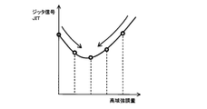
- FIG. 6 is a characteristic diagram illustrating an example of a relationship between a phase adjustment amount and a jitter amount.
- FIG. 6 is a characteristic diagram illustrating an example of a relationship between a phase adjustment amount, a high frequency enhancement amount, and a jitter amount. It is explanatory drawing which shows typically the reduction example of a window margin.
- FIG. 1 is a schematic diagram schematically illustrating a configuration of a main part of the data transmission / reception apparatus and the display apparatus according to the first embodiment.
- This display device is, for example, a TV (TeleVision) monitor, and thin film transistors for each pixel (not shown) are arranged in a matrix on the display screen (display unit) 12, and a gate driver (not shown) is provided for each thin film transistor group on a horizontal line. Each gate is simultaneously turned on simultaneously in the first period.
- a plurality of source drivers (data receiving units) 3 share the data signals sequentially with a second period shorter than the first period to each source for each thin film transistor group on the vertical line.
- the data transmission unit 2 is individually connected by a transmission line to a plurality of data reception units 3 arranged in parallel at the lower edge of the back side of the display screen 12.
- a plurality of transmission lines connecting the data transmission unit 2 and the data reception unit 3 constitute a data transmission unit 11.
- FIG. 2 is a block diagram illustrating a configuration example of main parts of the data transmission unit 2, the data reception unit 3, and the data transmission unit 11 illustrated in FIG.
- the data transmission unit 2, the data reception unit 3, and the data transmission unit 11 constitute a data transmission / reception device 1, and the data transmission unit 2 and the data reception unit 3 are connected via the data transmission unit 11.
- the data transmission unit 11 and the data transmission unit 2 are shown only in a portion corresponding to one data reception unit 3, but actually, the data transmission unit 11 and the data transmission unit 2 include a plurality of data transmission units 11 and data transmission units 2. Respectively corresponding to the data receiving unit 3.
- the data transmission unit 2 includes a data generation unit 4, a control unit 7, and a waveform equalization unit 6.
- the data generation unit 4 generates and outputs a clock signal TCLK and a data signal TDAT synchronized with the clock signal TCLK based on an externally provided video signal shared by the data reception unit 3.
- the control unit 7 generates and outputs a waveform control signal ECTRL based on the jitter signal JIT (indicating the amount of fluctuation on the time axis of the signal waveform) given from the data receiving unit 3.
- the waveform equalization unit (enhancement processing unit) 6 performs pre-emphasis processing (high frequency (frequency) enhancement processing) on the data signal TDAT based on the waveform control signal ECTRL provided from the control unit 7.
- the clock signal TCLK and the pre-emphasis-processed data signal EDAT are transmitted to the data reception unit 3 through the data transmission unit 11.
- the data reception unit 3 includes a data synchronization unit 8, a phase comparison unit 9, and a jitter detection unit 10.
- the data synchronization unit 8 receives the clock signal RCLK and the data signal RDAT transmitted by the data transmission unit 11, and determines 0/1 (L level / H level) of the data signal RDAT at the timing of the changing edge of the clock signal RCLK. .
- the phase comparison unit (output unit) 9 detects an absolute value phase error signal ABSER that is an absolute value of the phase error between the change edges of the data signal RDAT and the clock signal RCLK (with the phase error as a positive regardless of the delay / advance). To detect).
- the jitter detector (output unit) 10 calculates a jitter signal JIT that is a temporal average value of the absolute value phase error signal ABSER detected by the phase comparator 9.
- the jitter signal JIT calculated by the jitter detector 10 is given to the controller 7 of the data transmitter 2 through the data transmitter 11.
- the data generator 4 generates a clock signal TCLK and a data signal TDAT.
- the data signal TDAT forms unit bits in one cycle from the falling edge of the clock signal TCLK to the adjacent falling edge, and is a continuous 0/1 data string synchronized with the falling edge of the clock signal TCLK. Generated.
- the generated clock signal TCLK and data signal TDAT are received by the data synchronization unit 8 of the data reception unit 3 through the transmission line of the data transmission unit 11 and received data at the rising timing of the received clock signal RCLK.
- the signal RDAT is determined to be 0/1.
- the frequency of the transmission line depends on the resistance, inductance, parasitic capacitance, etc. Bandwidth is limited. As a result, as shown in FIG. 3, the distortion of the waveform of the received clock signal RCLK and data signal RDAT increases, resulting in a decrease in amplitude and a phase shift.
- the data transmission unit 2 synchronizes the data signal TDAT with the falling edge of the clock signal TCLK so that the determination of 0/1 of the received data signal RDAT can be reliably performed at the rising edge of the clock signal RCLK received by the data reception unit 3. And transmitted as a data string of 0/1 that changes.
- the data synchronization unit 8 The data signal RDAT cannot be correctly determined.
- the data synchronizer 8 on the receiving side uses a flip-flop to latch the data signal RDAT at the rising edge of the clock signal RCLK and determine 0/1 of the data signal RDAT.
- a determination error occurs when the setup time and hold time of the flip-flop cannot be satisfied due to the phase shift of the clock signal RCLK or the data signal RDAT.
- the determination error becomes screen noise in the liquid crystal display.
- the phase comparator 9 detects an absolute value phase error signal ABSER that is an absolute value of.
- the jitter detector 10 calculates a jitter signal JIT which is a temporal average value of the detected absolute value phase error signal ABSER so that the calculated jitter signal JIT is minimized, that is, the absolute value phase error signal ABSER is minimized.
- the control unit 7 generates and outputs a waveform control signal ECTRL so that
- FIG. 4 is a circuit diagram illustrating a specific configuration example of the data synchronization unit 8, the phase comparison unit 9, and the jitter detection unit 10.
- the data synchronizer 8 is composed of a D-type flip-flop.
- the data signal RDAT is supplied to the D (Data) terminal, the clock signal RCLK is supplied to the C (Clock) terminal, and the data at the rising edge of the clock signal RCLK.
- the 0/1 value of the signal RDAT is latched and output from the Q terminal.
- the phase comparison unit 9 includes a pulse gate 13, D-type flip-flops 14 and 15, and a logical product gate 16.
- the pulse gate 13 is supplied with the data signal RDAT, and when the rising edge or falling edge of the data signal RDAT is given, the pulse gate signal PG which becomes 0 for a half cycle of the clock signal TCLK starting from this edge timing. Is output.
- the flip-flop 14 always receives 1 at the D terminal, the pulse gate signal PG at the C terminal, and the output signal of the AND gate 16 at the R (Reset) terminal, and proceeds from the Q terminal to output the phase error signal LDER.
- the flip-flop 14 changes the Q terminal output from 0 to 1, and when the R terminal input becomes 1, the flip-flop 14 operates to return the Q terminal output to 0.
- the flip-flop 15 is always supplied with 1 at the D terminal, the clock signal RCLK at the C terminal, the output signal of the AND gate 16 at the R terminal, and the inverted signal of the pulse gate signal PG at the EN (ENable) terminal.
- the delayed phase error signal LGER is output from the terminal.
- the AND gate 16 is supplied with a phase error signal LDER from the Q terminal of the flip-flop 14 at one input terminal and a delayed phase error signal LGER from the Q terminal of the flip-flop 15 at the other input terminal.
- the AND gate 16 also provides an output signal to the R terminals of the flip-flops 14 and 15.
- the jitter detector 10 includes an OR gate 17, an FET (field effect transistor) 18, an impedance conversion amplifier 19, a capacitor 20, and a resistor 21.
- the OR gate 17 is provided with a phase error signal LDER from the Q terminal of the flip-flop 14 at one input terminal, and a delayed phase error signal LGER from the Q terminal of the flip-flop 15 at the other input terminal. From the absolute value phase error signal ABSER to the gate of the FET 18.
- the capacitor 20 and the resistor 21 are connected in parallel to form a charge / discharge circuit, and one terminal of the charge / discharge circuit is grounded.
- the FET 18 is connected between the control power supply and the other terminal of the charge / discharge circuit (20, 21), and the absolute value phase error signal ABSER is given to the gate from the output terminal of the OR gate 17.
- the FET 18, the capacitor 20, and the resistor 21 constitute a charge pump circuit that accumulates charges according to the absolute value phase error signal ABSER.
- the impedance conversion amplifier 19 has an input terminal connected to the other terminal of the charge / discharge circuit (20, 21), and outputs a jitter signal JIT from the output terminal.
- the jitter signal JIT is given to the control unit 7 of the data receiving unit 2 via the data transmission unit 11.
- the data synchronization unit 8 latches the 0/1 value of the data signal RDAT and outputs it as a synchronized data signal when the flip-flop is at the rising edge of the clock signal RCLK.
- the phase comparison unit 9 performs phase comparison between the rising edge of the data signal RDAT and the rising edge of the clock signal RCLK, and outputs a leading phase error signal LDER and a lagging phase error signal LGER.
- the changing edge of the data signal RDAT and the changing edge of the clock signal RCLK do not correspond one-to-one, it is necessary to select the changing edge of the clock signal RCLK corresponding to the changing edge of the data signal RDAT and perform phase comparison. .
- the pulse gate 13 is provided to realize this function.
- the pulse gate 13 starts from the time of the change and becomes 0 for a period of 1 ⁇ 2 period of the period T of the clock signal RCLK.
- the pulse gate signal PG returning to 1 is generated.
- the pulse gate signal PG is 1, and the Q terminal outputs of the flip-flops 14 and 15 are 0.
- the pulse gate signal PG transitions to 0 starting from the change time.
- the pulse gate signal PG becomes 0, the C terminal of the flip-flop 15 is enabled, and the input of the rising edge of the C terminal is accepted.
- the rising edge is input to the C terminal of the flip-flop 14 before the C terminal of the flip-flop 15.
- the terminal output first transitions from 0 to 1, and then the Q terminal output of the flip-flop 15 transitions from 0 to 1.
- the lead phase error signal LDER (the Q terminal output of the flip-flop 14) is set to 1 and output corresponding to the phase difference in which the phase of the data signal RDAT is advanced with respect to the phase of the clock signal RCLK.
- the rising edge is input to the C terminal of the flip-flop 15 before the C terminal of the flip-flop 14.
- the Q terminal output first transitions from 0 to 1, and then the Q terminal output of the flip-flop 14 transitions from 0 to 1.
- the output of the AND gate 16 becomes 1
- the flip-flops 14 and 15 are reset, and each Q terminal output of the flip-flops 14 and 15 instantaneously becomes 0.
- the delayed phase error signal LGER Q terminal output of the flip-flop 15 becomes 1 and is output corresponding to the phase difference in which the phase of the data signal RDAT is delayed with respect to the phase of the clock signal RCLK.
- the OR gate 17 logically adds the lead phase error signal LDER and the delay phase error signal LGER and outputs an absolute value phase error signal ABSER. That is, the OR gate 17 outputs the absolute value of the phase difference between the phase of the data signal RDAT and the phase of the clock signal RCLK.
- the absolute value phase error signal ABSER is 0.
- the absolute value phase The error signal ABSER becomes 1.
- the FET 18 is turned on, and the charge corresponding to the advance phase or the delay phase of the data signal RDAT is accumulated in the capacitor 20, and the terminal voltage of the capacitor 20 is accumulated. The voltage rises corresponding to the charged charge.
- the terminal voltage of the capacitor 20 will rise.
- a resistor 21 is connected in parallel to the capacitor 20, and the time constant for jitter detection is determined by discharging the charge with a constant time constant.
- the absolute value phase error signal ABSER is integrated, and the terminal voltage corresponding to the electric charge accumulated in the capacitor 20 is amplified by the impedance conversion amplifier 19 for impedance conversion.
- the jitter signal JIT is averaged in time series.
- the jitter signal JIT is given to the control unit 7 of the data receiving unit 2 via the data transmission unit 11.
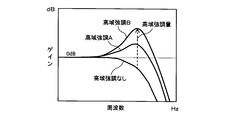
- the waveform equalization unit 6 reversely corrects the frequency phase characteristics of the band limitation in the transmission line of the data transmission unit 11 as shown in FIGS. 6, 7A and 7B.
- Such high frequency (frequency) enhancement processing pre-emphasis processing
- the control unit 7 controls the waveform control signal ECTRL for controlling the high-frequency emphasis amount of the waveform equalization unit 6 to thereby reduce jitter. It is preferable to control so that the signal JIT is minimized. This minimizes the phase shift between the data clock during transmission and maximizes the setup time and hold time during resynchronization, depending on variations in the characteristics of the transmission line and data transmission unit. Therefore, it is possible to reduce determination errors.
- FIG. 8 is a block diagram illustrating the main configuration of the data transmitting / receiving apparatus according to the second embodiment.
- the data transmission / reception device 1 a includes a data transmission unit 2 a, a data reception unit 3, and a data transmission unit 11, and the data transmission unit 2 a and the data reception unit 3 are connected via the data transmission unit 11.
- the data transmission unit 11 and the data transmission unit 2a corresponding to one data reception unit 3 are illustrated, but actually, the data transmission unit 11 and the data transmission unit 2a include a plurality of data transmission units 11 and data transmission units 2a. Respectively corresponding to the data receiving unit 3.
- the data transmission unit 2a includes a data generation unit 4, a control unit 7a, a phase adjustment unit 5, and a waveform equalization unit 6.
- the data generation unit 4 generates and outputs a clock signal TCLK and a data signal TDAT synchronized with the clock signal TCLK based on an externally provided video signal shared by the data reception unit 3.
- the control unit 7a generates and outputs a phase control signal PCCTRL and a waveform control signal ECTRL based on the jitter signal JIT given from the data receiving unit 3.
- the phase adjustment unit 5 delays the clock signal TCLK or the data signal TDAT based on the phase control signal PCCTRL given from the control unit 7a, and adjusts the relative phase between the output clock signal PCLK and the data signal PDAT.
- the waveform equalization unit 6 performs high frequency (frequency) enhancement processing (pre-emphasis processing) on the data signal PDAT based on the waveform control signal ECTRL supplied from the control unit 7a.
- the clock signal PCLK and the data signal EDAT subjected to high frequency emphasis processing are transmitted through the data transmission unit 11.
- the clock signal PCLK and the data signal EDAT transmitted through the data transmission unit 11 are received by the data reception unit 3 as the clock signal RCLK and the data signal RDAT.
- the control unit 7a is configured so that the jitter signal JIT calculated by the jitter detecting unit 10 of the receiving unit 3 is minimized, that is, the absolute value phase error signal ABSER is minimized.
- a phase control signal PCCTRL and a waveform control signal ECTRL are generated and output.
- the waveform equalization unit 6 Based on the waveform control signal ECTRL, the waveform equalization unit 6 performs high-frequency emphasis processing that reversely corrects the band-limited frequency phase characteristics in the transmission line before data transmission, as shown in FIGS. 6, 7A, and 7B. By applying, phase shift can be suppressed.
- the high frequency emphasis processing since there is an optimum value of the high frequency emphasis amount, it is preferable to control the waveform control signal ECTRL by the control unit 7a so that the jitter signal JIT is minimized. . Thereby, a phase shift can be suppressed to the minimum and a determination error can be reduced.
- the phase adjuster 5 generates a clock signal PCLK or a data signal PDAT obtained by delaying the clock signal TCLK or the data signal TDAT based on the phase control signal PCCTRL and adjusts the phase. Thereby, a phase shift can be suppressed to the minimum.
- a phase shift can be suppressed to the minimum.
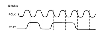
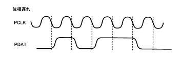
- the delayed clock signal PCLK or data signal PDAT With respect to the phase shift between the clock signal RCLK and the data signal RDAT input to the data synchronizer 8, so-called skew, as shown in FIGS. 9A, 9B, and 9C, the delayed clock signal PCLK or data signal PDAT. To adjust the phase. Thereby, the phase shift between the clock signal RCLK and the data signal RDAT can be suppressed to the minimum.
- the control unit 7a controls the phase control signal PCTRL so that the jitter signal JIT is minimized. It is preferable to do. This minimizes the phase shift, maximizes the setup time and hold time during resynchronization, and reduces decision errors regardless of variations in the characteristics of the transmission line and data transmission unit. Is possible.
- the control of the high frequency emphasis amount of the waveform equalization unit 6 and the control of the phase adjustment amount of the phase adjustment unit 5 may cause the optimum value of the other to be shifted as shown in FIG. For this reason, it is preferable that the adjustment is not performed independently but simultaneously. For example, it is preferable to search in a matrix manner for a total N ⁇ M points of N points for the phase adjustment amount and M points for the high frequency emphasis amount, and to find and set an optimum point at which the jitter signal is minimized.
- an optimal point can be searched at high speed by using a method such as a hill-climbing method and a re-steep descent method in addition to the N ⁇ M point matrix full search.
- the other configuration and operation of the data transmission / reception device 1a are the same as the configuration and operation of the data transmission / reception device 1 described in the first embodiment, and a description thereof will be omitted.
- the present invention can be used for a liquid crystal display device and an organic EL display device used in a television receiver, a personal computer, and the like.
Landscapes
- Engineering & Computer Science (AREA)
- Computer Networks & Wireless Communication (AREA)
- Signal Processing (AREA)
- Power Engineering (AREA)
- Control Of Indicators Other Than Cathode Ray Tubes (AREA)
Abstract
伝送線路及び送信側の特性に依らず、再同期化しデータ信号を判定する時のフリップフロップのセットアップ時間及びホールド時間を最大化できるデータ送受信装置を提供する。 クロック信号、及びクロック信号に同期したデータ信号を生成するデータ生成部4と、データ伝送部11が伝送したクロック信号及びデータ信号を受信し、クロック信号の変化エッジに基づきデータ信号がHレベル又はLレベルかを判定するデータ同期部8と、データ伝送部11が伝送したクロック信号及びデータ信号の各変化エッジ間の位相誤差の絶対値を検出し、絶対値に基づくジッタ信号を出力する出力部9,10と、出力部9,10が出力したジッタ信号が最小となるように、データ生成部4が生成したデータ信号の高域周波数強調度を調整する波形制御信号を出力する制御部7と、制御部7が出力した波形制御信号に基づきデータ信号を高域周波数強調処理する強調処理部6とを備えている。
Description
本発明は、クロック信号、及びクロック信号に同期したデータ信号を生成して伝送し、伝送したクロック信号及びデータ信号を受信して、データ信号のハイ又はローを判定するデータ送受信装置、及びこのデータ送受信装置を備える表示装置に関するものである。
液晶表示装置及び有機EL表示装置等の表示装置では、表示画面に画素毎の薄膜トランジスタがマトリクス状に配置されている。このような表示画面では、例えば、横方向の線上の薄膜トランジスタ群毎に、ゲートドライバが各ゲートを同時に第1周期で順次オンにして行き、縦方向の線上の薄膜トランジスタ群毎に、ソースドライバが各ソースに同時に第1周期より短い第2周期で画素データ信号を順次与えて行く。
近年、液晶表示装置の高解像度化及び多階調化等の技術進展に伴い、液晶コントローラからソースドライバに伝送する情報量が急激に増大して来ており、パラレル伝送方式では信号線数が増加する為、Point-to-Point接続の低振幅・高速差動データ伝送方式が採用されている。
特許文献1には、クロック信号から複数の異なる位相のタップ出力信号をストローブ信号として出力するPLL(Phase Locked Loop)回路を備え、シリアル伝送データとクロック信号とのスキュー(位相誤差)を検出し、最適なタイミングのストローブ信号を選択して設定するシリアル・パラレル変換装置が開示されている。
上述したような低振幅・高速差動データ伝送方式のデータ送受信装置では、表示装置の大画面化が進み、液晶コントローラからソースドライバ迄の距離が長くなると、液晶コントローラ及びソースドライバ間での伝送品質劣化が大きくなり、また伝送線路の特性ばらつきも大きくなる。その為、受信側のデータラッチ回路(フリップフロップ)のセットアップ時間及びホールド時間を満たすことが難しくなって来ている。
例えば、設計試作時に最適調整して仕様を満足できたとしても、量産ばらつきまで考慮すると、図12に示すように、伝送データ信号のアイパターンが劣化して、ウィンドウマージン(タイミングマージン、電圧マージン)を確保することが困難になるという問題がある。
例えば、設計試作時に最適調整して仕様を満足できたとしても、量産ばらつきまで考慮すると、図12に示すように、伝送データ信号のアイパターンが劣化して、ウィンドウマージン(タイミングマージン、電圧マージン)を確保することが困難になるという問題がある。
また、特許文献1に開示されたシリアル・パラレル変換装置では、液晶パネルの長辺側に複数配置されるドライバのそれぞれにPLL回路を搭載する必要があり、ドライバの回路規模が大きくなり、狭額縁化の阻害要因になるという問題がある。また、液晶パネルの幅広い領域に渡って配置されるソースドライバのそれぞれが発振器を含むPLL回路を備える必要があり、不要電磁波の輻射が増大するという問題がある。
本発明は、上述したような事情に鑑みてなされたものであり、伝送線路及びデータ送信部の特性ばらつきに依らず、再同期化してデータ信号を判定する時のフリップフロップのセットアップ時間及びホールド時間を最大化できるデータ送受信装置を提供することを目的とする。
また、本発明は、本発明に係るデータ送受信装置を備える表示装置を提供することを目的とする。
また、本発明は、本発明に係るデータ送受信装置を備える表示装置を提供することを目的とする。
本発明に係るデータ送受信装置は、クロック信号、及び該クロック信号に同期したデータ信号を生成するデータ生成部と、該データ生成部が生成したクロック信号及びデータ信号を伝送するデータ伝送部と、該データ伝送部が伝送したクロック信号及びデータ信号を受信し、該クロック信号の変化エッジに基づき前記データ信号がHレベル又はLレベルかを判定するデータ同期部と、前記データ伝送部が伝送したクロック信号及びデータ信号の各変化エッジ間の位相誤差の絶対値を検出し、該絶対値に基づくジッタ信号を出力する出力部と、該出力部が出力したジッタ信号が最小となるように、前記データ生成部が生成したデータ信号の高域周波数強調度を調整する波形制御信号を出力する制御部と、該制御部が出力した波形制御信号に基づき前記データ信号を高域周波数強調処理する強調処理部とを備えることを特徴とする。
本発明に係るデータ送受信装置は、前記データ生成部が生成したクロック信号及びデータ信号間の位相を調整する位相調整部を更に備え、前記制御部は、前記ジッタ信号が最小となるように、前記位相調整部が位相を調整する為の位相制御信号を更に出力するように構成してあることを特徴とする。
本発明に係る表示装置は、本発明に係るデータ送受信装置と、該データ送受信装置が送受信したデータ信号に基づく画像を表示する表示部とを備えることを特徴とする。
本発明に係るデータ送受信装置によれば、伝送線路及びデータ送信部の特性ばらつきに依らず、再同期化してデータ信号を判定する時のフリップフロップのセットアップ時間及びホールド時間を最大化できる。また、これにより、安定した高速データ伝送が可能となり、更に、データ受信部にPLL回路等の大規模回路を配置する必要が無いので、表示装置の狭額縁化、及び不要電磁波輻射の増大防止を図ることができる。
本発明に係る表示装置によれば、伝送線路及びデータ送信部の特性ばらつきに依らず、再同期化してデータ信号を判定する時のフリップフロップのセットアップ時間及びホールド時間を最大化できる。また、これにより、安定した高速データ伝送が可能となり、更に、データ受信部にPLL回路等の大規模回路を配置する必要が無いので、表示装置の狭額縁化、及び不要電磁波輻射の増大防止を図ることができる。
以下に、本発明をその実施例を示す図面に基づいて説明する。
図1は、データ送受信装置及び表示装置の実施例1の要部構成を模式的に示す模式図である。
この表示装置は、例えばTV(TeleVision)モニタであり、表示画面(表示部)12に図示しない画素毎の薄膜トランジスタがマトリクス状に配置され、横方向の線上の薄膜トランジスタ群毎に、図示しないゲートドライバが各ゲートを同時に第1周期で順次オンにする。また、複数のソースドライバ(データ受信部)3が分担して、縦方向の線上の薄膜トランジスタ群毎に、各ソースに同時に第1周期より短い第2周期でデータ信号を順次与える。
この表示装置は、例えばTV(TeleVision)モニタであり、表示画面(表示部)12に図示しない画素毎の薄膜トランジスタがマトリクス状に配置され、横方向の線上の薄膜トランジスタ群毎に、図示しないゲートドライバが各ゲートを同時に第1周期で順次オンにする。また、複数のソースドライバ(データ受信部)3が分担して、縦方向の線上の薄膜トランジスタ群毎に、各ソースに同時に第1周期より短い第2周期でデータ信号を順次与える。
表示画面12の裏側には、本実施例1に係るデータ送受信装置を構成するデータ送信部2、データ受信部3及びデータ伝送部11が設けられている。データ送信部2は、表示画面12の裏側下部の縁辺部に並設された複数のデータ受信部3と伝送線路により個別に接続されている。データ送信部2及びデータ受信部3間を接続する複数の伝送線路はデータ伝送部11を構成している。
図2は、図1に示すデータ送信部2、データ受信部3及びデータ伝送部11の要部構成例を示すブロック図である。
このデータ送信部2、データ受信部3及びデータ伝送部11は、データ送受信装置1を構成しており、データ伝送部11を介して、データ送信部2及びデータ受信部3が接続されている。尚、ここでは、データ伝送部11及びデータ送信部2は、1つのデータ受信部3に対応する部分のみを図示しているが、実際には、データ伝送部11及びデータ送信部2は、複数のデータ受信部3にそれぞれ対応している。
このデータ送信部2、データ受信部3及びデータ伝送部11は、データ送受信装置1を構成しており、データ伝送部11を介して、データ送信部2及びデータ受信部3が接続されている。尚、ここでは、データ伝送部11及びデータ送信部2は、1つのデータ受信部3に対応する部分のみを図示しているが、実際には、データ伝送部11及びデータ送信部2は、複数のデータ受信部3にそれぞれ対応している。
データ送信部2は、データ生成部4、制御部7及び波形等化部6を備えている。
データ生成部4は、データ受信部3が分担する外部から与えられた映像信号に基づき、クロック信号TCLK、及びクロック信号TCLKに同期したデータ信号TDATを生成して出力する。
制御部7は、データ受信部3から与えられたジッタ信号JIT(信号波形の時間軸上の揺らぎ量を示す)に基づき、波形制御信号ECTRLを生成して出力する。
波形等化部(強調処理部)6は、制御部7から与えられた波形制御信号ECTRLに基づき、データ信号TDATをプリエンファシス処理(高域(周波数)強調処理)する。
クロック信号TCLK、及びプリエンファシス処理されたデータ信号EDATは、データ伝送部11を通じて、データ受信部3へ送信される。
データ生成部4は、データ受信部3が分担する外部から与えられた映像信号に基づき、クロック信号TCLK、及びクロック信号TCLKに同期したデータ信号TDATを生成して出力する。
制御部7は、データ受信部3から与えられたジッタ信号JIT(信号波形の時間軸上の揺らぎ量を示す)に基づき、波形制御信号ECTRLを生成して出力する。
波形等化部(強調処理部)6は、制御部7から与えられた波形制御信号ECTRLに基づき、データ信号TDATをプリエンファシス処理(高域(周波数)強調処理)する。
クロック信号TCLK、及びプリエンファシス処理されたデータ信号EDATは、データ伝送部11を通じて、データ受信部3へ送信される。
データ受信部3は、データ同期部8、位相比較部9及びジッタ検出部10を備えている。
データ同期部8は、データ伝送部11が伝送したクロック信号RCLK及びデータ信号RDATを受信し、クロック信号RCLKの変化エッジのタイミングでデータ信号RDATの0/1(Lレベル/Hレベル)を判定する。
データ同期部8は、データ伝送部11が伝送したクロック信号RCLK及びデータ信号RDATを受信し、クロック信号RCLKの変化エッジのタイミングでデータ信号RDATの0/1(Lレベル/Hレベル)を判定する。
位相比較部(出力部)9は、データ信号RDAT及びクロック信号RCLKの変化エッジ間の位相誤差の絶対値である絶対値位相誤差信号ABSERを検出する(遅れ/進みに関係なく位相誤差をプラスとして検出する)。
ジッタ検出部(出力部)10は、位相比較部9が検出した絶対値位相誤差信号ABSERの時間的平均値であるジッタ信号JITを演算する。
ジッタ検出部10が演算したジッタ信号JITは、データ伝送部11を通じて、データ送信部2の制御部7に与えられる。
ジッタ検出部(出力部)10は、位相比較部9が検出した絶対値位相誤差信号ABSERの時間的平均値であるジッタ信号JITを演算する。
ジッタ検出部10が演算したジッタ信号JITは、データ伝送部11を通じて、データ送信部2の制御部7に与えられる。
以下に、このような構成のデータ送受信装置1の動作例を、それを示す図3のタイミングチャートを参照しながら説明する。
データ生成部4でクロック信号TCLK及びデータ信号TDATが生成される。
ここで、データ信号TDATは、クロック信号TCLKの立ち下がりから隣接する立ち下がり迄の1周期で単位ビットを構成しており、クロック信号TCLKの立ち下がりに同期した連続する0/1のデータ列として生成される。
データ生成部4でクロック信号TCLK及びデータ信号TDATが生成される。
ここで、データ信号TDATは、クロック信号TCLKの立ち下がりから隣接する立ち下がり迄の1周期で単位ビットを構成しており、クロック信号TCLKの立ち下がりに同期した連続する0/1のデータ列として生成される。
生成されたクロック信号TCLK及びデータ信号TDATは、データ伝送部11の伝送線路を通じて、データ受信部3のデータ同期部8で受信され、受信されたクロック信号RCLKの立ち上がりのタイミングで、受信されたデータ信号RDATの0/1の判定を行う。
データ生成部4が生成したクロック信号TCLK及びデータ信号TDATを、例えば大型液晶パネル等においてコントロールICからドライバICまで長距離伝送する場合、伝送線路の抵抗、インダクタンス及び寄生容量等により、伝送線路の周波数帯域が制限される。これにより、図3に示すように、受信されたクロック信号RCLK及びデータ信号RDATの波形の歪が大きくなり、振幅低下及び位相シフトが発生する。
データ生成部4が生成したクロック信号TCLK及びデータ信号TDATを、例えば大型液晶パネル等においてコントロールICからドライバICまで長距離伝送する場合、伝送線路の抵抗、インダクタンス及び寄生容量等により、伝送線路の周波数帯域が制限される。これにより、図3に示すように、受信されたクロック信号RCLK及びデータ信号RDATの波形の歪が大きくなり、振幅低下及び位相シフトが発生する。
近年、液晶ディスプレイの高解像度化が進み、データ量が増大するに伴い、クロック信号TCLKとデータ信号TDATの伝送周波数が数GHzと高速化して来ている。また、液晶ディスプレイの大画面化が進んで伝送線路が長くなるに伴い、伝送線路の周波数帯域が制限されて、伝送信号品質が劣化して来ている。
データ受信部3で受信したクロック信号RCLKの立ち上がりで,受信したデータ信号RDATの0/1の判定が確実にできるよう、データ送信部2は、データ信号TDATをクロック信号TCLKの立ち下がりに同期して遷移する0/1のデータ列として送信する。しかし、伝送線路により信号波形が劣化して歪が大きくなり、信号振幅の低下及び位相シフト量が大きくなって、データを判定するタイミングでのアイパターンのウィンドウマージンが小さくなると、データ同期部8でのデータ信号RDATの判定が正しく行えなくなる。
通常、受信側のデータ同期部8では、フリップフロップを用いてクロック信号RCLKの立ち上がりエッジでデータ信号RDATをラッチして、データ信号RDATの0/1の判定を行う。しかし、クロック信号RCLK又はデータ信号RDATの位相シフトにより、フリップフロップのセットアップ時間、ホールド時間を満たせなくなると、判定エラーが発生する。判定エラーは、液晶ディスプレイにおいては画面ノイズとなる。
上記の問題を解決する為、本実施例1においては、図2,3に示すように、データ同期部8に入力されるクロック信号RCLKの立ち下がりエッジとデータ信号RDATの変化エッジとの位相誤差の絶対値である絶対値位相誤差信号ABSERを位相比較部9が検出する。次いで、検出した絶対値位相誤差信号ABSERの時間的平均値であるジッタ信号JITをジッタ検出部10が演算し、演算したジッタ信号JITが最小となるように、即ち絶対値位相誤差信号ABSERが最小となるように、制御部7が波形制御信号ECTRLを生成し出力する。
図4は、データ同期部8、位相比較部9及びジッタ検出部10の具体的な構成例を示す回路図である。
データ同期部8は、D型フリップフロップで構成され、D(Data)端子にデータ信号RDATが、C(Clock)端子にクロック信号RCLKがそれぞれ与えられ、クロック信号RCLKの立ち上がりエッジのときの、データ信号RDATの0/1値をラッチしてQ端子から出力する。
データ同期部8は、D型フリップフロップで構成され、D(Data)端子にデータ信号RDATが、C(Clock)端子にクロック信号RCLKがそれぞれ与えられ、クロック信号RCLKの立ち上がりエッジのときの、データ信号RDATの0/1値をラッチしてQ端子から出力する。
位相比較部9は、パルスゲート13、D型フリップフロップ14,15、論理積ゲート16を備えている。
パルスゲート13は、データ信号RDATを与えられ、データ信号RDATの立ち上がりエッジ又は立ち下がりエッジが与えられた時に、このエッジタイミングを起点としてクロック信号TCLKの1/2周期間0となるパルスゲート信号PGを出力する。
パルスゲート13は、データ信号RDATを与えられ、データ信号RDATの立ち上がりエッジ又は立ち下がりエッジが与えられた時に、このエッジタイミングを起点としてクロック信号TCLKの1/2周期間0となるパルスゲート信号PGを出力する。
フリップフロップ14は、D端子に常に1が、C端子にパルスゲート信号PGが、R(Reset)端子に論理積ゲート16の出力信号が与えられ、Q端子から進み位相誤差信号LDERを出力する。フリップフロップ14は、C端子に立ち上がりエッジが入力されると、Q端子出力を0から1に遷移させ、R端子入力が1になると、Q端子出力を0に戻すように動作する。
フリップフロップ15は、D端子に常に1が、C端子にクロック信号RCLKが、R端子に論理積ゲート16の出力信号が、EN(ENable)端子にパルスゲート信号PGの反転信号が与えられ、Q端子から遅れ位相誤差信号LGERを出力する。
フリップフロップ15は、EN端子に立ち上がりエッジ(パルスゲート信号PGの立ち下がりエッジ)が入力されると、C端子への立ち上がりエッジの入力待ち状態(C端子のイネーブル状態)になる。そして、C端子に立ち上がりエッジが入力されると、Q端子出力を0から1に遷移させて、C端子への立ち上がりエッジの入力を受け付けない状態(C端子のディスエーブル状態)になる。また、R端子入力が1になると、Q端子出力を0に戻すように動作する。
フリップフロップ15は、EN端子に立ち上がりエッジ(パルスゲート信号PGの立ち下がりエッジ)が入力されると、C端子への立ち上がりエッジの入力待ち状態(C端子のイネーブル状態)になる。そして、C端子に立ち上がりエッジが入力されると、Q端子出力を0から1に遷移させて、C端子への立ち上がりエッジの入力を受け付けない状態(C端子のディスエーブル状態)になる。また、R端子入力が1になると、Q端子出力を0に戻すように動作する。
論理積ゲート16は、一方の入力端子に、フリップフロップ14のQ端子から進み位相誤差信号LDERが、他方の入力端子に、フリップフロップ15のQ端子から遅れ位相誤差信号LGERが与えられる。論理積ゲート16は、また、出力信号をフリップフロップ14,15のR端子に与える。
ジッタ検出部10は、論理和ゲート17、FET(電界効果トランジスタ)18、インピーダンス変換アンプ19、コンデンサ20及び抵抗21を備えている。
論理和ゲート17は、一方の入力端子に、フリップフロップ14のQ端子から進み位相誤差信号LDERが、他方の入力端子に、フリップフロップ15のQ端子から遅れ位相誤差信号LGERが与えられ、出力端子から絶対値位相誤差信号ABSERをFET18のゲートに与える。
論理和ゲート17は、一方の入力端子に、フリップフロップ14のQ端子から進み位相誤差信号LDERが、他方の入力端子に、フリップフロップ15のQ端子から遅れ位相誤差信号LGERが与えられ、出力端子から絶対値位相誤差信号ABSERをFET18のゲートに与える。
コンデンサ20及び抵抗21は、並列に接続されて充放電回路を構成しており、この充放電回路の一方の端子は接地されている。
FET18は、制御電源、及び充放電回路(20,21)の他方の端子間に接続され、ゲートに論理和ゲート17の出力端子から絶対値位相誤差信号ABSERが与えられる。FET18、コンデンサ20及び抵抗21は、絶対値位相誤差信号ABSERに応じて電荷を蓄積するチャージポンプ回路を構成している。
インピーダンス変換アンプ19は、入力端子に充放電回路(20,21)の他方の端子が接続され、出力端子からジッタ信号JITを出力する。ジッタ信号JITは、データ伝送部11を経由して、データ受信部2の制御部7に与えられる。
FET18は、制御電源、及び充放電回路(20,21)の他方の端子間に接続され、ゲートに論理和ゲート17の出力端子から絶対値位相誤差信号ABSERが与えられる。FET18、コンデンサ20及び抵抗21は、絶対値位相誤差信号ABSERに応じて電荷を蓄積するチャージポンプ回路を構成している。
インピーダンス変換アンプ19は、入力端子に充放電回路(20,21)の他方の端子が接続され、出力端子からジッタ信号JITを出力する。ジッタ信号JITは、データ伝送部11を経由して、データ受信部2の制御部7に与えられる。
このような構成のデータ同期部8、位相比較部9及びジッタ検出部10の具体的な動作を、それを示す図3のタイミングチャートを参照しながら説明する。
データ同期部8は、フリップフロップが、クロック信号RCLKの立ち上がりエッジの時に、データ信号RDATの0/1値をラッチして、同期化データ信号として出力する。
データ同期部8は、フリップフロップが、クロック信号RCLKの立ち上がりエッジの時に、データ信号RDATの0/1値をラッチして、同期化データ信号として出力する。
位相比較部9では、データ信号RDATの立ち上がりエッジとクロック信号RCLKの立ち上がりエッジとの位相比較を行い、進み位相誤差信号LDER及び遅れ位相誤差信号LGERを出力する。但し、データ信号RDATの変化エッジとクロック信号RCLKの変化エッジとは1対1に対応しない為、データ信号RDATの変化エッジに対応するクロック信号RCLKの変化エッジを選択して位相比較する必要がある。パルスゲート13は、この機能を実現する為に設けられている。
パルスゲート13は、データ信号RDATが1から0に、又は0から1に変化すると、その変化時点を起点として、クロック信号RCLKの周期Tの1/2周期の期間だけ0となった後、元の1に戻るパルスゲート信号PGを生成する。
データ信号RDATのレベル変化が無い初期状態においては、パルスゲート信号PGは1、フリップフロップ14,15のQ端子出力は0である。データ信号RDATが1から0に、又は0から1に変化すると、変化時点を起点として、パルスゲート信号PGが0に遷移する。パルスゲート信号PGが0になると、フリップフロップ15のC端子がイネーブル状態となり、C端子の立ち上がりエッジの入力を受け付ける状態となる。
データ信号RDATのレベル変化が無い初期状態においては、パルスゲート信号PGは1、フリップフロップ14,15のQ端子出力は0である。データ信号RDATが1から0に、又は0から1に変化すると、変化時点を起点として、パルスゲート信号PGが0に遷移する。パルスゲート信号PGが0になると、フリップフロップ15のC端子がイネーブル状態となり、C端子の立ち上がりエッジの入力を受け付ける状態となる。
データ信号RDATの位相が、クロック信号RCLKの位相よりも進んでいるときは、フリップフロップ15のC端子よりも先にフリップフロップ14のC端子に立ち上がりエッジが入力される為、フリップフロップ14のQ端子出力が先に0から1に遷移し、その後、フリップフロップ15のQ端子出力が0から1に遷移する。フリップフロップ14,15のQ端子出力が共に1になると、論理積ゲート16の出力が1となり、フリップフロップ14,15がリセットされて、フリップフロップ14,15の各Q端子出力が瞬時に0となる。
以上の動作により、データ信号RDATの位相がクロック信号RCLKの位相に対して進んでいる位相差に対応して、進み位相誤差信号LDER(フリップフロップ14のQ端子出力)が1となり出力される。
以上の動作により、データ信号RDATの位相がクロック信号RCLKの位相に対して進んでいる位相差に対応して、進み位相誤差信号LDER(フリップフロップ14のQ端子出力)が1となり出力される。
また、データ信号RDATの位相が、クロック信号RCLKの位相よりも遅れているときは、フリップフロップ14のC端子よりも先にフリップフロップ15のC端子に立ち上がりエッジが入力される為、フリップフロップ15のQ端子出力が先に0から1に遷移し、その後、フリップフロップ14のQ端子出力が0から1に遷移する。フリップフロップ14,15のQ端子出力が共に1になると、論理積ゲート16の出力が1となり、フリップフロップ14,15がリセットされて、フリップフロップ14,15の各Q端子出力が瞬時に0となる。
以上の動作により、データ信号RDATの位相がクロック信号RCLKの位相に対して遅れている位相差に対応して、遅れ位相誤差信号LGER(フリップフロップ15のQ端子出力)が1となり出力される。
以上の動作により、データ信号RDATの位相がクロック信号RCLKの位相に対して遅れている位相差に対応して、遅れ位相誤差信号LGER(フリップフロップ15のQ端子出力)が1となり出力される。
ジッタ検出部10において、論理和ゲート17は、進み位相誤差信号LDERと遅れ位相誤差信号LGERとを論理加算して、絶対値位相誤差信号ABSERを出力する。即ち、論理和ゲート17は、データ信号RDATの位相とクロック信号RCLKの位相との位相差の絶対値を出力することになる。進み位相誤差信号LDERと遅れ位相誤差信号LGERが共に0のときは、絶対値位相誤差信号ABSERは0となり、進み位相誤差信号LDER又は遅れ位相誤差信号LGERの何れかが1となると、絶対値位相誤差信号ABSERが1となる。
そして、絶対値位相誤差信号ABSERが1の期間は、FET18がオンとなり、データ信号RDATの進み位相分又は遅れ位相分に相当する電荷がコンデンサ20に蓄積され、コンデンサ20の端子電圧は、蓄積された電荷に対応する電圧に上昇する。データ信号RDATとクロック信号RCLKとの位相差(位相進みであるか位相遅れであるかは問わない)が大きい程、絶対値位相誤差信号ABSERが1の期間、即ちFET18がオンの期間が長くなり、コンデンサ20の端子電圧は上昇することになる。
また、コンデンサ20には抵抗21が並列に接続されており、一定の時定数で電荷を放電することで、ジッタ検出の時定数を決定する。
また、コンデンサ20には抵抗21が並列に接続されており、一定の時定数で電荷を放電することで、ジッタ検出の時定数を決定する。
以上の動作により、図5のタイミングチャートに示すように、絶対値位相誤差信号ABSERが積分され、コンデンサ20に蓄積された電荷に対応する端子電圧は、インピーダンス変換するインピーダンス変換アンプ19により電流増幅されて、時系列的に平均化されたジッタ信号JITとなる。ジッタ信号JITは、データ伝送部11を経由して、データ受信部2の制御部7に与えられる。
受信されたデータ信号RDATの振幅低下に関しては、波形等化部6において、図6、図7A,図7Bに示すように、データ伝送部11の伝送線路における帯域制限の周波数位相特性を逆補正するような高域(周波数)強調処理(プリエンファシス処理)を施す。これにより、位相シフトを抑制することができる。
尚、高域強調処理に関しては、高域強調量の最適値が存在する為、制御部7にて波形等化部6の高域強調量を制御する波形制御信号ECTRLを制御することで,ジッタ信号JITが最小となるように制御することが好ましい。これにより、伝送時のデータ・クロック間の位相シフトを最小限に抑制して、再同期化時におけるセットアップ時間及びホールド時間を最大化することができ、伝送線路及びデータ送信部の特性ばらつきに依らず、判定エラーを低減することが可能である。
尚、高域強調処理に関しては、高域強調量の最適値が存在する為、制御部7にて波形等化部6の高域強調量を制御する波形制御信号ECTRLを制御することで,ジッタ信号JITが最小となるように制御することが好ましい。これにより、伝送時のデータ・クロック間の位相シフトを最小限に抑制して、再同期化時におけるセットアップ時間及びホールド時間を最大化することができ、伝送線路及びデータ送信部の特性ばらつきに依らず、判定エラーを低減することが可能である。
図8は、データ送受信装置の実施例2の要部構成を示すブロック図である。
このデータ送受信装置1aは、データ送信部2a、データ受信部3及びデータ伝送部11により構成されており、データ伝送部11を介して、データ送信部2a及びデータ受信部3が接続されている。尚、ここでは、データ伝送部11及びデータ送信部2aは、1つのデータ受信部3に対応する部分のみを図示しているが、実際には、データ伝送部11及びデータ送信部2aは、複数のデータ受信部3にそれぞれ対応している。
このデータ送受信装置1aは、データ送信部2a、データ受信部3及びデータ伝送部11により構成されており、データ伝送部11を介して、データ送信部2a及びデータ受信部3が接続されている。尚、ここでは、データ伝送部11及びデータ送信部2aは、1つのデータ受信部3に対応する部分のみを図示しているが、実際には、データ伝送部11及びデータ送信部2aは、複数のデータ受信部3にそれぞれ対応している。
データ送信部2aは、データ生成部4、制御部7a、位相調整部5及び波形等化部6を備えている。
データ生成部4は、データ受信部3が分担する外部から与えられた映像信号に基づき、クロック信号TCLK、及びクロック信号TCLKに同期したデータ信号TDATを生成して出力する。
データ生成部4は、データ受信部3が分担する外部から与えられた映像信号に基づき、クロック信号TCLK、及びクロック信号TCLKに同期したデータ信号TDATを生成して出力する。
制御部7aは、データ受信部3から与えられたジッタ信号JITに基づき、位相制御信号PCTRL及び波形制御信号ECTRLを生成して出力する。
位相調整部5は、制御部7aから与えられた位相制御信号PCTRLに基づき、クロック信号TCLK又はデータ信号TDATを遅延させて、出力するクロック信号PCLK及びデータ信号PDAT間の相対位相を調整する。
位相調整部5は、制御部7aから与えられた位相制御信号PCTRLに基づき、クロック信号TCLK又はデータ信号TDATを遅延させて、出力するクロック信号PCLK及びデータ信号PDAT間の相対位相を調整する。
波形等化部6は、制御部7aから与えられた波形制御信号ECTRLに基づき、データ信号PDATを高域(周波数)強調処理(プリエンファシス処理)する。
クロック信号PCLK、及び高域強調処理されたデータ信号EDATは、データ伝送部11を通じて送信される。データ伝送部11を通じて送信されたクロック信号PCLK及びデータ信号EDATは、クロック信号RCLK及びデータ信号RDATとしてデータ受信部3で受信される。
クロック信号PCLK、及び高域強調処理されたデータ信号EDATは、データ伝送部11を通じて送信される。データ伝送部11を通じて送信されたクロック信号PCLK及びデータ信号EDATは、クロック信号RCLK及びデータ信号RDATとしてデータ受信部3で受信される。
このような構成のデータ送受信装置1aでは、受信部3のジッタ検出部10が演算したジッタ信号JITが最小となるように、即ち絶対値位相誤差信号ABSERが最小となるように、制御部7aが位相制御信号PCTRL及び波形制御信号ECTRLを生成し出力する。
波形等化部6は、波形制御信号ECTRLに基づき、図6、図7A、図7Bに示すように、データ伝送前に伝送線路における帯域制限の周波数位相特性を逆補正するような高域強調処理を施すことにより、位相シフトを抑制することができる。
波形等化部6は、波形制御信号ECTRLに基づき、図6、図7A、図7Bに示すように、データ伝送前に伝送線路における帯域制限の周波数位相特性を逆補正するような高域強調処理を施すことにより、位相シフトを抑制することができる。
つまり、高域強調処理に関しては、高域強調量の最適値が存在するので、制御部7aにて波形制御信号ECTRLを制御することにより、ジッタ信号JITが最小となるように制御することが好ましい。これにより、位相シフトを最小限に抑制して、判定エラーを低減することができる。
位相調整部5は、位相制御信号PCTRLに基づき、クロック信号TCLK又はデータ信号TDATを遅延させたクロック信号PCLK又はデータ信号PDATを生成して位相調整する。これにより、位相シフトを最小限に抑制することができる。
データ同期部8に入力されるクロック信号RCLKとデータ信号RDATとの間の位相シフト、所謂スキューに関しては、図9A、図9B、図9Cに示すように、遅延させたクロック信号PCLK又はデータ信号PDATを生成して位相調整する。これにより、クロック信号RCLKとデータ信号RDATとの間の位相シフトを最小限に抑制することができる。
データ同期部8に入力されるクロック信号RCLKとデータ信号RDATとの間の位相シフト、所謂スキューに関しては、図9A、図9B、図9Cに示すように、遅延させたクロック信号PCLK又はデータ信号PDATを生成して位相調整する。これにより、クロック信号RCLKとデータ信号RDATとの間の位相シフトを最小限に抑制することができる。
つまり、位相調整に関しては、図10に示すように、位相調整量の最適値が存在するので、制御部7aにて位相制御信号PCTRLを制御することにより、ジッタ信号JITが最小となるように制御することが好ましい。これにより、位相シフトを最小限に抑制して、再同期化時におけるセットアップ時間及びホールド時間を最大化することができ、伝送線路及びデータ送信部の特性ばらつきに依らず、判定エラーを低減することが可能である。
また、波形等化部6の高域強調量の制御と位相調整部5の位相調整量の制御とは、図11に示すように、一方を調整すると他方の最適値がずれてしまうことがある為、独立して調整を行うのではなく、同時に調整することが好ましい。例えば、位相調整量をN点、高域強調量をM点の合計N×M点をマトリクス的に探査し、ジッタ信号が最小となる最適点を求めて設定することが好ましい。
尚、最小点探査には、N×M点のマトリクス全探査の他に、山登り法、再急降下法等の方法を用いることで、高速に最適点を探査することができる。
このデータ送受信装置1aのその他の構成及び動作は、実施例1において説明したデータ送受信装置1の構成及び動作と同様であるので、説明を省略する。
このデータ送受信装置1aのその他の構成及び動作は、実施例1において説明したデータ送受信装置1の構成及び動作と同様であるので、説明を省略する。
本実施例1,2は、全ての点で例示であって制限的なものではないと考えるべきである。本発明の範囲は上述の説明ではなく請求の範囲によって示され、請求の範囲と均等の意味及び範囲内での全ての変更が含まれることが意図される。
本発明は、テレビジョン受像機、パーソナルコンピュータ等に使用される液晶表示装置及び有機EL表示装置等に利用することができる。
1,1a データ送受信装置
2,2a データ送信部
3 データ受信部
4 データ生成部
5 位相調整部
6 波形等化部(強調処理部)
7,7a 制御部
8 データ同期部
9 位相比較部(出力部)
10 ジッタ検出部(出力部)
11 データ伝送部
12 表示画面(表示部)
13 パルスゲート
14,15 D型フリップフロップ
16 論理積ゲート
17 論理和ゲート
18 FET
19 インピーダンス変換アンプ
20 コンデンサ
21 抵抗
2,2a データ送信部
3 データ受信部
4 データ生成部
5 位相調整部
6 波形等化部(強調処理部)
7,7a 制御部
8 データ同期部
9 位相比較部(出力部)
10 ジッタ検出部(出力部)
11 データ伝送部
12 表示画面(表示部)
13 パルスゲート
14,15 D型フリップフロップ
16 論理積ゲート
17 論理和ゲート
18 FET
19 インピーダンス変換アンプ
20 コンデンサ
21 抵抗
Claims (3)
- クロック信号、及び該クロック信号に同期したデータ信号を生成するデータ生成部と、
該データ生成部が生成したクロック信号及びデータ信号を伝送するデータ伝送部と、
該データ伝送部が伝送したクロック信号及びデータ信号を受信し、該クロック信号の変化エッジに基づき前記データ信号がHレベル又はLレベルかを判定するデータ同期部と、
前記データ伝送部が伝送したクロック信号及びデータ信号の各変化エッジ間の位相誤差の絶対値を検出し、該絶対値に基づくジッタ信号を出力する出力部と、
該出力部が出力したジッタ信号が最小となるように、前記データ生成部が生成したデータ信号の高域周波数強調度を調整する波形制御信号を出力する制御部と、
該制御部が出力した波形制御信号に基づき前記データ信号を高域周波数強調処理する強調処理部と
を備えることを特徴とするデータ送受信装置。 - 前記データ生成部が生成したクロック信号及びデータ信号間の位相を調整する位相調整部を更に備え、
前記制御部は、前記ジッタ信号が最小となるように、前記位相調整部が位相を調整する為の位相制御信号を更に出力するように構成してある請求項1に記載のデータ送受信装置。 - 請求項1又は2に記載されたデータ送受信装置と、
該データ送受信装置が送受信したデータ信号に基づく画像を表示する表示部と
を備えることを特徴とする表示装置。
Priority Applications (1)
| Application Number | Priority Date | Filing Date | Title |
|---|---|---|---|
| PCT/JP2015/082612 WO2017085845A1 (ja) | 2015-11-19 | 2015-11-19 | データ送受信装置及び表示装置 |
Applications Claiming Priority (1)
| Application Number | Priority Date | Filing Date | Title |
|---|---|---|---|
| PCT/JP2015/082612 WO2017085845A1 (ja) | 2015-11-19 | 2015-11-19 | データ送受信装置及び表示装置 |
Publications (1)
| Publication Number | Publication Date |
|---|---|
| WO2017085845A1 true WO2017085845A1 (ja) | 2017-05-26 |
Family
ID=58719265
Family Applications (1)
| Application Number | Title | Priority Date | Filing Date |
|---|---|---|---|
| PCT/JP2015/082612 Ceased WO2017085845A1 (ja) | 2015-11-19 | 2015-11-19 | データ送受信装置及び表示装置 |
Country Status (1)
| Country | Link |
|---|---|
| WO (1) | WO2017085845A1 (ja) |
Citations (3)
| Publication number | Priority date | Publication date | Assignee | Title |
|---|---|---|---|---|
| JP2001339374A (ja) * | 2000-05-29 | 2001-12-07 | Hitachi Ltd | ビット同期装置およびその方法 |
| JP2007124130A (ja) * | 2005-10-26 | 2007-05-17 | Fuji Xerox Co Ltd | 送信装置、受信装置、及び送受信装置 |
| JP2015146536A (ja) * | 2014-02-03 | 2015-08-13 | 富士通株式会社 | 情報処理システムおよびパラメータ調整方法 |
-
2015
- 2015-11-19 WO PCT/JP2015/082612 patent/WO2017085845A1/ja not_active Ceased
Patent Citations (3)
| Publication number | Priority date | Publication date | Assignee | Title |
|---|---|---|---|---|
| JP2001339374A (ja) * | 2000-05-29 | 2001-12-07 | Hitachi Ltd | ビット同期装置およびその方法 |
| JP2007124130A (ja) * | 2005-10-26 | 2007-05-17 | Fuji Xerox Co Ltd | 送信装置、受信装置、及び送受信装置 |
| JP2015146536A (ja) * | 2014-02-03 | 2015-08-13 | 富士通株式会社 | 情報処理システムおよびパラメータ調整方法 |
Similar Documents
| Publication | Publication Date | Title |
|---|---|---|
| US8884934B2 (en) | Display driving system using single level data transmission with embedded clock signal | |
| TWI556205B (zh) | 信號傳送與接收系統及相關顯示器之時序控制器 | |
| JP6410281B2 (ja) | データ送受信装置及び表示装置 | |
| US12401489B2 (en) | Clock and data recovery circuit and a display apparatus having the same | |
| CN102184696B (zh) | 具有时脉相位/数据相位自动调整机制的显示器及其驱动方法 | |
| US9355054B2 (en) | Digital calibration-based skew cancellation for long-reach MIPI D-PHY serial links | |
| US8362996B2 (en) | Display with CLK phase auto-adjusting mechanism and method of driving same | |
| US9356589B2 (en) | Interchannel skew adjustment circuit | |
| US20130113777A1 (en) | Method of transferring data in a display device | |
| KR20150077811A (ko) | 표시장치와 그 구동 방법 | |
| US9576550B2 (en) | Data interface method and apparatus using de-skew function | |
| US11223468B1 (en) | Receiver circuit performing adaptive equalization and system including the same | |
| JP2011233216A (ja) | 半導体システムのデータ送受信装置および方法 | |
| TW201505379A (zh) | 時脈資料回復方法以及時脈資料回復電路 | |
| CN112053662B (zh) | 用来传送数据的方法、时序控制器以及显示系统 | |
| US20160365071A1 (en) | Display device and driving method thereof | |
| CN104283665A (zh) | 用于传送数据的系统和包括其的视频显示器 | |
| US9197229B2 (en) | Panel driving circuit and ring oscillator clock automatic synchronization method thereof | |
| US9813070B2 (en) | Display apparatus and driving method for the same | |
| TWI410949B (zh) | 資料驅動器與用以決定資料驅動器之最佳偏移之方法 | |
| KR20100078604A (ko) | 데이터 송신 및 수신 장치들 | |
| CN103997335B (zh) | 时序控制器的信号频率的设定装置、方法以及显示设备 | |
| JP5503207B2 (ja) | 送信機および通信システム | |
| CN106952600B (zh) | 时序控制器及其信号输出方法 | |
| KR102419352B1 (ko) | 표시장치, 데이터 구동부 및 스큐 보정 방법 |
Legal Events
| Date | Code | Title | Description |
|---|---|---|---|
| 121 | Ep: the epo has been informed by wipo that ep was designated in this application |
Ref document number: 15908785 Country of ref document: EP Kind code of ref document: A1 |
|
| NENP | Non-entry into the national phase |
Ref country code: DE |
|
| 122 | Ep: pct application non-entry in european phase |
Ref document number: 15908785 Country of ref document: EP Kind code of ref document: A1 |
|
| NENP | Non-entry into the national phase |
Ref country code: JP |