WO2017082368A1 - Laminate and laminate manufacturing method - Google Patents
Laminate and laminate manufacturing method Download PDFInfo
- Publication number
- WO2017082368A1 WO2017082368A1 PCT/JP2016/083438 JP2016083438W WO2017082368A1 WO 2017082368 A1 WO2017082368 A1 WO 2017082368A1 JP 2016083438 W JP2016083438 W JP 2016083438W WO 2017082368 A1 WO2017082368 A1 WO 2017082368A1
- Authority
- WO
- WIPO (PCT)
- Prior art keywords
- copper powder
- mass
- metal
- base material
- intermediate layer
- Prior art date
Links
Images


Classifications
-
- B—PERFORMING OPERATIONS; TRANSPORTING
- B32—LAYERED PRODUCTS
- B32B—LAYERED PRODUCTS, i.e. PRODUCTS BUILT-UP OF STRATA OF FLAT OR NON-FLAT, e.g. CELLULAR OR HONEYCOMB, FORM
- B32B15/00—Layered products comprising a layer of metal
- B32B15/01—Layered products comprising a layer of metal all layers being exclusively metallic
-
- B—PERFORMING OPERATIONS; TRANSPORTING
- B32—LAYERED PRODUCTS
- B32B—LAYERED PRODUCTS, i.e. PRODUCTS BUILT-UP OF STRATA OF FLAT OR NON-FLAT, e.g. CELLULAR OR HONEYCOMB, FORM
- B32B9/00—Layered products comprising a layer of a particular substance not covered by groups B32B11/00 - B32B29/00
- B32B9/04—Layered products comprising a layer of a particular substance not covered by groups B32B11/00 - B32B29/00 comprising such particular substance as the main or only constituent of a layer, which is next to another layer of the same or of a different material
- B32B9/041—Layered products comprising a layer of a particular substance not covered by groups B32B11/00 - B32B29/00 comprising such particular substance as the main or only constituent of a layer, which is next to another layer of the same or of a different material of metal
-
- B—PERFORMING OPERATIONS; TRANSPORTING
- B05—SPRAYING OR ATOMISING IN GENERAL; APPLYING FLUENT MATERIALS TO SURFACES, IN GENERAL
- B05D—PROCESSES FOR APPLYING FLUENT MATERIALS TO SURFACES, IN GENERAL
- B05D1/00—Processes for applying liquids or other fluent materials
- B05D1/02—Processes for applying liquids or other fluent materials performed by spraying
- B05D1/12—Applying particulate materials
-
- B—PERFORMING OPERATIONS; TRANSPORTING
- B05—SPRAYING OR ATOMISING IN GENERAL; APPLYING FLUENT MATERIALS TO SURFACES, IN GENERAL
- B05D—PROCESSES FOR APPLYING FLUENT MATERIALS TO SURFACES, IN GENERAL
- B05D7/00—Processes, other than flocking, specially adapted for applying liquids or other fluent materials to particular surfaces or for applying particular liquids or other fluent materials
- B05D7/24—Processes, other than flocking, specially adapted for applying liquids or other fluent materials to particular surfaces or for applying particular liquids or other fluent materials for applying particular liquids or other fluent materials
-
- B—PERFORMING OPERATIONS; TRANSPORTING
- B22—CASTING; POWDER METALLURGY
- B22F—WORKING METALLIC POWDER; MANUFACTURE OF ARTICLES FROM METALLIC POWDER; MAKING METALLIC POWDER; APPARATUS OR DEVICES SPECIALLY ADAPTED FOR METALLIC POWDER
- B22F1/00—Metallic powder; Treatment of metallic powder, e.g. to facilitate working or to improve properties
- B22F1/14—Treatment of metallic powder
- B22F1/142—Thermal or thermo-mechanical treatment
-
- B—PERFORMING OPERATIONS; TRANSPORTING
- B22—CASTING; POWDER METALLURGY
- B22F—WORKING METALLIC POWDER; MANUFACTURE OF ARTICLES FROM METALLIC POWDER; MAKING METALLIC POWDER; APPARATUS OR DEVICES SPECIALLY ADAPTED FOR METALLIC POWDER
- B22F9/00—Making metallic powder or suspensions thereof
- B22F9/02—Making metallic powder or suspensions thereof using physical processes
- B22F9/06—Making metallic powder or suspensions thereof using physical processes starting from liquid material
- B22F9/08—Making metallic powder or suspensions thereof using physical processes starting from liquid material by casting, e.g. through sieves or in water, by atomising or spraying
- B22F9/082—Making metallic powder or suspensions thereof using physical processes starting from liquid material by casting, e.g. through sieves or in water, by atomising or spraying atomising using a fluid
-
- B—PERFORMING OPERATIONS; TRANSPORTING
- B32—LAYERED PRODUCTS
- B32B—LAYERED PRODUCTS, i.e. PRODUCTS BUILT-UP OF STRATA OF FLAT OR NON-FLAT, e.g. CELLULAR OR HONEYCOMB, FORM
- B32B15/00—Layered products comprising a layer of metal
- B32B15/01—Layered products comprising a layer of metal all layers being exclusively metallic
- B32B15/013—Layered products comprising a layer of metal all layers being exclusively metallic one layer being formed of an iron alloy or steel, another layer being formed of a metal other than iron or aluminium
- B32B15/015—Layered products comprising a layer of metal all layers being exclusively metallic one layer being formed of an iron alloy or steel, another layer being formed of a metal other than iron or aluminium the said other metal being copper or nickel or an alloy thereof
-
- B—PERFORMING OPERATIONS; TRANSPORTING
- B32—LAYERED PRODUCTS
- B32B—LAYERED PRODUCTS, i.e. PRODUCTS BUILT-UP OF STRATA OF FLAT OR NON-FLAT, e.g. CELLULAR OR HONEYCOMB, FORM
- B32B15/00—Layered products comprising a layer of metal
- B32B15/02—Layer formed of wires, e.g. mesh
-
- B—PERFORMING OPERATIONS; TRANSPORTING
- B32—LAYERED PRODUCTS
- B32B—LAYERED PRODUCTS, i.e. PRODUCTS BUILT-UP OF STRATA OF FLAT OR NON-FLAT, e.g. CELLULAR OR HONEYCOMB, FORM
- B32B15/00—Layered products comprising a layer of metal
- B32B15/04—Layered products comprising a layer of metal comprising metal as the main or only constituent of a layer, which is next to another layer of the same or of a different material
- B32B15/043—Layered products comprising a layer of metal comprising metal as the main or only constituent of a layer, which is next to another layer of the same or of a different material of metal
-
- B—PERFORMING OPERATIONS; TRANSPORTING
- B32—LAYERED PRODUCTS
- B32B—LAYERED PRODUCTS, i.e. PRODUCTS BUILT-UP OF STRATA OF FLAT OR NON-FLAT, e.g. CELLULAR OR HONEYCOMB, FORM
- B32B15/00—Layered products comprising a layer of metal
- B32B15/04—Layered products comprising a layer of metal comprising metal as the main or only constituent of a layer, which is next to another layer of the same or of a different material
- B32B15/08—Layered products comprising a layer of metal comprising metal as the main or only constituent of a layer, which is next to another layer of the same or of a different material of synthetic resin
-
- B—PERFORMING OPERATIONS; TRANSPORTING
- B32—LAYERED PRODUCTS
- B32B—LAYERED PRODUCTS, i.e. PRODUCTS BUILT-UP OF STRATA OF FLAT OR NON-FLAT, e.g. CELLULAR OR HONEYCOMB, FORM
- B32B15/00—Layered products comprising a layer of metal
- B32B15/20—Layered products comprising a layer of metal comprising aluminium or copper
-
- B—PERFORMING OPERATIONS; TRANSPORTING
- B32—LAYERED PRODUCTS
- B32B—LAYERED PRODUCTS, i.e. PRODUCTS BUILT-UP OF STRATA OF FLAT OR NON-FLAT, e.g. CELLULAR OR HONEYCOMB, FORM
- B32B27/00—Layered products comprising a layer of synthetic resin
- B32B27/06—Layered products comprising a layer of synthetic resin as the main or only constituent of a layer, which is next to another layer of the same or of a different material
-
- B—PERFORMING OPERATIONS; TRANSPORTING
- B32—LAYERED PRODUCTS
- B32B—LAYERED PRODUCTS, i.e. PRODUCTS BUILT-UP OF STRATA OF FLAT OR NON-FLAT, e.g. CELLULAR OR HONEYCOMB, FORM
- B32B27/00—Layered products comprising a layer of synthetic resin
- B32B27/18—Layered products comprising a layer of synthetic resin characterised by the use of special additives
- B32B27/20—Layered products comprising a layer of synthetic resin characterised by the use of special additives using fillers, pigments, thixotroping agents
-
- B—PERFORMING OPERATIONS; TRANSPORTING
- B32—LAYERED PRODUCTS
- B32B—LAYERED PRODUCTS, i.e. PRODUCTS BUILT-UP OF STRATA OF FLAT OR NON-FLAT, e.g. CELLULAR OR HONEYCOMB, FORM
- B32B3/00—Layered products comprising a layer with external or internal discontinuities or unevennesses, or a layer of non-planar form; Layered products having particular features of form
- B32B3/26—Layered products comprising a layer with external or internal discontinuities or unevennesses, or a layer of non-planar form; Layered products having particular features of form characterised by a particular shape of the outline of the cross-section of a continuous layer; characterised by a layer with cavities or internal voids ; characterised by an apertured layer
- B32B3/263—Layered products comprising a layer with external or internal discontinuities or unevennesses, or a layer of non-planar form; Layered products having particular features of form characterised by a particular shape of the outline of the cross-section of a continuous layer; characterised by a layer with cavities or internal voids ; characterised by an apertured layer characterised by a layer having non-uniform thickness
-
- B—PERFORMING OPERATIONS; TRANSPORTING
- B32—LAYERED PRODUCTS
- B32B—LAYERED PRODUCTS, i.e. PRODUCTS BUILT-UP OF STRATA OF FLAT OR NON-FLAT, e.g. CELLULAR OR HONEYCOMB, FORM
- B32B3/00—Layered products comprising a layer with external or internal discontinuities or unevennesses, or a layer of non-planar form; Layered products having particular features of form
- B32B3/26—Layered products comprising a layer with external or internal discontinuities or unevennesses, or a layer of non-planar form; Layered products having particular features of form characterised by a particular shape of the outline of the cross-section of a continuous layer; characterised by a layer with cavities or internal voids ; characterised by an apertured layer
- B32B3/30—Layered products comprising a layer with external or internal discontinuities or unevennesses, or a layer of non-planar form; Layered products having particular features of form characterised by a particular shape of the outline of the cross-section of a continuous layer; characterised by a layer with cavities or internal voids ; characterised by an apertured layer characterised by a layer formed with recesses or projections, e.g. hollows, grooves, protuberances, ribs
-
- B—PERFORMING OPERATIONS; TRANSPORTING
- B32—LAYERED PRODUCTS
- B32B—LAYERED PRODUCTS, i.e. PRODUCTS BUILT-UP OF STRATA OF FLAT OR NON-FLAT, e.g. CELLULAR OR HONEYCOMB, FORM
- B32B37/00—Methods or apparatus for laminating, e.g. by curing or by ultrasonic bonding
- B32B37/14—Methods or apparatus for laminating, e.g. by curing or by ultrasonic bonding characterised by the properties of the layers
- B32B37/16—Methods or apparatus for laminating, e.g. by curing or by ultrasonic bonding characterised by the properties of the layers with all layers existing as coherent layers before laminating
- B32B37/18—Methods or apparatus for laminating, e.g. by curing or by ultrasonic bonding characterised by the properties of the layers with all layers existing as coherent layers before laminating involving the assembly of discrete sheets or panels only
-
- B—PERFORMING OPERATIONS; TRANSPORTING
- B32—LAYERED PRODUCTS
- B32B—LAYERED PRODUCTS, i.e. PRODUCTS BUILT-UP OF STRATA OF FLAT OR NON-FLAT, e.g. CELLULAR OR HONEYCOMB, FORM
- B32B37/00—Methods or apparatus for laminating, e.g. by curing or by ultrasonic bonding
- B32B37/14—Methods or apparatus for laminating, e.g. by curing or by ultrasonic bonding characterised by the properties of the layers
- B32B37/24—Methods or apparatus for laminating, e.g. by curing or by ultrasonic bonding characterised by the properties of the layers with at least one layer not being coherent before laminating, e.g. made up from granular material sprinkled onto a substrate
-
- B—PERFORMING OPERATIONS; TRANSPORTING
- B32—LAYERED PRODUCTS
- B32B—LAYERED PRODUCTS, i.e. PRODUCTS BUILT-UP OF STRATA OF FLAT OR NON-FLAT, e.g. CELLULAR OR HONEYCOMB, FORM
- B32B5/00—Layered products characterised by the non- homogeneity or physical structure, i.e. comprising a fibrous, filamentary, particulate or foam layer; Layered products characterised by having a layer differing constitutionally or physically in different parts
- B32B5/16—Layered products characterised by the non- homogeneity or physical structure, i.e. comprising a fibrous, filamentary, particulate or foam layer; Layered products characterised by having a layer differing constitutionally or physically in different parts characterised by features of a layer formed of particles, e.g. chips, powder or granules
-
- B—PERFORMING OPERATIONS; TRANSPORTING
- B32—LAYERED PRODUCTS
- B32B—LAYERED PRODUCTS, i.e. PRODUCTS BUILT-UP OF STRATA OF FLAT OR NON-FLAT, e.g. CELLULAR OR HONEYCOMB, FORM
- B32B7/00—Layered products characterised by the relation between layers; Layered products characterised by the relative orientation of features between layers, or by the relative values of a measurable parameter between layers, i.e. products comprising layers having different physical, chemical or physicochemical properties; Layered products characterised by the interconnection of layers
-
- B—PERFORMING OPERATIONS; TRANSPORTING
- B32—LAYERED PRODUCTS
- B32B—LAYERED PRODUCTS, i.e. PRODUCTS BUILT-UP OF STRATA OF FLAT OR NON-FLAT, e.g. CELLULAR OR HONEYCOMB, FORM
- B32B9/00—Layered products comprising a layer of a particular substance not covered by groups B32B11/00 - B32B29/00
- B32B9/005—Layered products comprising a layer of a particular substance not covered by groups B32B11/00 - B32B29/00 comprising one layer of ceramic material, e.g. porcelain, ceramic tile
-
- C—CHEMISTRY; METALLURGY
- C04—CEMENTS; CONCRETE; ARTIFICIAL STONE; CERAMICS; REFRACTORIES
- C04B—LIME, MAGNESIA; SLAG; CEMENTS; COMPOSITIONS THEREOF, e.g. MORTARS, CONCRETE OR LIKE BUILDING MATERIALS; ARTIFICIAL STONE; CERAMICS; REFRACTORIES; TREATMENT OF NATURAL STONE
- C04B41/00—After-treatment of mortars, concrete, artificial stone or ceramics; Treatment of natural stone
- C04B41/80—After-treatment of mortars, concrete, artificial stone or ceramics; Treatment of natural stone of only ceramics
- C04B41/81—Coating or impregnation
- C04B41/89—Coating or impregnation for obtaining at least two superposed coatings having different compositions
- C04B41/90—Coating or impregnation for obtaining at least two superposed coatings having different compositions at least one coating being a metal
-
- C—CHEMISTRY; METALLURGY
- C22—METALLURGY; FERROUS OR NON-FERROUS ALLOYS; TREATMENT OF ALLOYS OR NON-FERROUS METALS
- C22C—ALLOYS
- C22C9/00—Alloys based on copper
-
- C—CHEMISTRY; METALLURGY
- C23—COATING METALLIC MATERIAL; COATING MATERIAL WITH METALLIC MATERIAL; CHEMICAL SURFACE TREATMENT; DIFFUSION TREATMENT OF METALLIC MATERIAL; COATING BY VACUUM EVAPORATION, BY SPUTTERING, BY ION IMPLANTATION OR BY CHEMICAL VAPOUR DEPOSITION, IN GENERAL; INHIBITING CORROSION OF METALLIC MATERIAL OR INCRUSTATION IN GENERAL
- C23C—COATING METALLIC MATERIAL; COATING MATERIAL WITH METALLIC MATERIAL; SURFACE TREATMENT OF METALLIC MATERIAL BY DIFFUSION INTO THE SURFACE, BY CHEMICAL CONVERSION OR SUBSTITUTION; COATING BY VACUUM EVAPORATION, BY SPUTTERING, BY ION IMPLANTATION OR BY CHEMICAL VAPOUR DEPOSITION, IN GENERAL
- C23C24/00—Coating starting from inorganic powder
- C23C24/02—Coating starting from inorganic powder by application of pressure only
- C23C24/04—Impact or kinetic deposition of particles
-
- C—CHEMISTRY; METALLURGY
- C23—COATING METALLIC MATERIAL; COATING MATERIAL WITH METALLIC MATERIAL; CHEMICAL SURFACE TREATMENT; DIFFUSION TREATMENT OF METALLIC MATERIAL; COATING BY VACUUM EVAPORATION, BY SPUTTERING, BY ION IMPLANTATION OR BY CHEMICAL VAPOUR DEPOSITION, IN GENERAL; INHIBITING CORROSION OF METALLIC MATERIAL OR INCRUSTATION IN GENERAL
- C23C—COATING METALLIC MATERIAL; COATING MATERIAL WITH METALLIC MATERIAL; SURFACE TREATMENT OF METALLIC MATERIAL BY DIFFUSION INTO THE SURFACE, BY CHEMICAL CONVERSION OR SUBSTITUTION; COATING BY VACUUM EVAPORATION, BY SPUTTERING, BY ION IMPLANTATION OR BY CHEMICAL VAPOUR DEPOSITION, IN GENERAL
- C23C24/00—Coating starting from inorganic powder
- C23C24/08—Coating starting from inorganic powder by application of heat or pressure and heat
- C23C24/082—Coating starting from inorganic powder by application of heat or pressure and heat without intermediate formation of a liquid in the layer
- C23C24/085—Coating with metallic material, i.e. metals or metal alloys, optionally comprising hard particles, e.g. oxides, carbides or nitrides
- C23C24/087—Coating with metal alloys or metal elements only
-
- C—CHEMISTRY; METALLURGY
- C23—COATING METALLIC MATERIAL; COATING MATERIAL WITH METALLIC MATERIAL; CHEMICAL SURFACE TREATMENT; DIFFUSION TREATMENT OF METALLIC MATERIAL; COATING BY VACUUM EVAPORATION, BY SPUTTERING, BY ION IMPLANTATION OR BY CHEMICAL VAPOUR DEPOSITION, IN GENERAL; INHIBITING CORROSION OF METALLIC MATERIAL OR INCRUSTATION IN GENERAL
- C23C—COATING METALLIC MATERIAL; COATING MATERIAL WITH METALLIC MATERIAL; SURFACE TREATMENT OF METALLIC MATERIAL BY DIFFUSION INTO THE SURFACE, BY CHEMICAL CONVERSION OR SUBSTITUTION; COATING BY VACUUM EVAPORATION, BY SPUTTERING, BY ION IMPLANTATION OR BY CHEMICAL VAPOUR DEPOSITION, IN GENERAL
- C23C24/00—Coating starting from inorganic powder
- C23C24/08—Coating starting from inorganic powder by application of heat or pressure and heat
- C23C24/10—Coating starting from inorganic powder by application of heat or pressure and heat with intermediate formation of a liquid phase in the layer
- C23C24/103—Coating with metallic material, i.e. metals or metal alloys, optionally comprising hard particles, e.g. oxides, carbides or nitrides
-
- C—CHEMISTRY; METALLURGY
- C23—COATING METALLIC MATERIAL; COATING MATERIAL WITH METALLIC MATERIAL; CHEMICAL SURFACE TREATMENT; DIFFUSION TREATMENT OF METALLIC MATERIAL; COATING BY VACUUM EVAPORATION, BY SPUTTERING, BY ION IMPLANTATION OR BY CHEMICAL VAPOUR DEPOSITION, IN GENERAL; INHIBITING CORROSION OF METALLIC MATERIAL OR INCRUSTATION IN GENERAL
- C23C—COATING METALLIC MATERIAL; COATING MATERIAL WITH METALLIC MATERIAL; SURFACE TREATMENT OF METALLIC MATERIAL BY DIFFUSION INTO THE SURFACE, BY CHEMICAL CONVERSION OR SUBSTITUTION; COATING BY VACUUM EVAPORATION, BY SPUTTERING, BY ION IMPLANTATION OR BY CHEMICAL VAPOUR DEPOSITION, IN GENERAL
- C23C28/00—Coating for obtaining at least two superposed coatings either by methods not provided for in a single one of groups C23C2/00 - C23C26/00 or by combinations of methods provided for in subclasses C23C and C25C or C25D
- C23C28/02—Coating for obtaining at least two superposed coatings either by methods not provided for in a single one of groups C23C2/00 - C23C26/00 or by combinations of methods provided for in subclasses C23C and C25C or C25D only coatings only including layers of metallic material
- C23C28/021—Coating for obtaining at least two superposed coatings either by methods not provided for in a single one of groups C23C2/00 - C23C26/00 or by combinations of methods provided for in subclasses C23C and C25C or C25D only coatings only including layers of metallic material including at least one metal alloy layer
-
- C—CHEMISTRY; METALLURGY
- C23—COATING METALLIC MATERIAL; COATING MATERIAL WITH METALLIC MATERIAL; CHEMICAL SURFACE TREATMENT; DIFFUSION TREATMENT OF METALLIC MATERIAL; COATING BY VACUUM EVAPORATION, BY SPUTTERING, BY ION IMPLANTATION OR BY CHEMICAL VAPOUR DEPOSITION, IN GENERAL; INHIBITING CORROSION OF METALLIC MATERIAL OR INCRUSTATION IN GENERAL
- C23C—COATING METALLIC MATERIAL; COATING MATERIAL WITH METALLIC MATERIAL; SURFACE TREATMENT OF METALLIC MATERIAL BY DIFFUSION INTO THE SURFACE, BY CHEMICAL CONVERSION OR SUBSTITUTION; COATING BY VACUUM EVAPORATION, BY SPUTTERING, BY ION IMPLANTATION OR BY CHEMICAL VAPOUR DEPOSITION, IN GENERAL
- C23C28/00—Coating for obtaining at least two superposed coatings either by methods not provided for in a single one of groups C23C2/00 - C23C26/00 or by combinations of methods provided for in subclasses C23C and C25C or C25D
- C23C28/02—Coating for obtaining at least two superposed coatings either by methods not provided for in a single one of groups C23C2/00 - C23C26/00 or by combinations of methods provided for in subclasses C23C and C25C or C25D only coatings only including layers of metallic material
- C23C28/023—Coating for obtaining at least two superposed coatings either by methods not provided for in a single one of groups C23C2/00 - C23C26/00 or by combinations of methods provided for in subclasses C23C and C25C or C25D only coatings only including layers of metallic material only coatings of metal elements only
-
- C—CHEMISTRY; METALLURGY
- C23—COATING METALLIC MATERIAL; COATING MATERIAL WITH METALLIC MATERIAL; CHEMICAL SURFACE TREATMENT; DIFFUSION TREATMENT OF METALLIC MATERIAL; COATING BY VACUUM EVAPORATION, BY SPUTTERING, BY ION IMPLANTATION OR BY CHEMICAL VAPOUR DEPOSITION, IN GENERAL; INHIBITING CORROSION OF METALLIC MATERIAL OR INCRUSTATION IN GENERAL
- C23C—COATING METALLIC MATERIAL; COATING MATERIAL WITH METALLIC MATERIAL; SURFACE TREATMENT OF METALLIC MATERIAL BY DIFFUSION INTO THE SURFACE, BY CHEMICAL CONVERSION OR SUBSTITUTION; COATING BY VACUUM EVAPORATION, BY SPUTTERING, BY ION IMPLANTATION OR BY CHEMICAL VAPOUR DEPOSITION, IN GENERAL
- C23C30/00—Coating with metallic material characterised only by the composition of the metallic material, i.e. not characterised by the coating process
- C23C30/005—Coating with metallic material characterised only by the composition of the metallic material, i.e. not characterised by the coating process on hard metal substrates
-
- H—ELECTRICITY
- H01—ELECTRIC ELEMENTS
- H01L—SEMICONDUCTOR DEVICES NOT COVERED BY CLASS H10
- H01L21/00—Processes or apparatus adapted for the manufacture or treatment of semiconductor or solid state devices or of parts thereof
- H01L21/02—Manufacture or treatment of semiconductor devices or of parts thereof
- H01L21/04—Manufacture or treatment of semiconductor devices or of parts thereof the devices having at least one potential-jump barrier or surface barrier, e.g. PN junction, depletion layer or carrier concentration layer
- H01L21/48—Manufacture or treatment of parts, e.g. containers, prior to assembly of the devices, using processes not provided for in a single one of the subgroups H01L21/06 - H01L21/326
- H01L21/4814—Conductive parts
- H01L21/4871—Bases, plates or heatsinks
- H01L21/4882—Assembly of heatsink parts
-
- H—ELECTRICITY
- H01—ELECTRIC ELEMENTS
- H01L—SEMICONDUCTOR DEVICES NOT COVERED BY CLASS H10
- H01L23/00—Details of semiconductor or other solid state devices
- H01L23/34—Arrangements for cooling, heating, ventilating or temperature compensation ; Temperature sensing arrangements
- H01L23/36—Selection of materials, or shaping, to facilitate cooling or heating, e.g. heatsinks
- H01L23/373—Cooling facilitated by selection of materials for the device or materials for thermal expansion adaptation, e.g. carbon
- H01L23/3735—Laminates or multilayers, e.g. direct bond copper ceramic substrates
-
- B—PERFORMING OPERATIONS; TRANSPORTING
- B22—CASTING; POWDER METALLURGY
- B22F—WORKING METALLIC POWDER; MANUFACTURE OF ARTICLES FROM METALLIC POWDER; MAKING METALLIC POWDER; APPARATUS OR DEVICES SPECIALLY ADAPTED FOR METALLIC POWDER
- B22F7/00—Manufacture of composite layers, workpieces, or articles, comprising metallic powder, by sintering the powder, with or without compacting wherein at least one part is obtained by sintering or compression
- B22F7/02—Manufacture of composite layers, workpieces, or articles, comprising metallic powder, by sintering the powder, with or without compacting wherein at least one part is obtained by sintering or compression of composite layers
- B22F7/04—Manufacture of composite layers, workpieces, or articles, comprising metallic powder, by sintering the powder, with or without compacting wherein at least one part is obtained by sintering or compression of composite layers with one or more layers not made from powder, e.g. made from solid metal
- B22F2007/042—Manufacture of composite layers, workpieces, or articles, comprising metallic powder, by sintering the powder, with or without compacting wherein at least one part is obtained by sintering or compression of composite layers with one or more layers not made from powder, e.g. made from solid metal characterised by the layer forming method
-
- B—PERFORMING OPERATIONS; TRANSPORTING
- B22—CASTING; POWDER METALLURGY
- B22F—WORKING METALLIC POWDER; MANUFACTURE OF ARTICLES FROM METALLIC POWDER; MAKING METALLIC POWDER; APPARATUS OR DEVICES SPECIALLY ADAPTED FOR METALLIC POWDER
- B22F9/00—Making metallic powder or suspensions thereof
- B22F9/02—Making metallic powder or suspensions thereof using physical processes
- B22F9/06—Making metallic powder or suspensions thereof using physical processes starting from liquid material
- B22F9/08—Making metallic powder or suspensions thereof using physical processes starting from liquid material by casting, e.g. through sieves or in water, by atomising or spraying
- B22F9/082—Making metallic powder or suspensions thereof using physical processes starting from liquid material by casting, e.g. through sieves or in water, by atomising or spraying atomising using a fluid
- B22F2009/0824—Making metallic powder or suspensions thereof using physical processes starting from liquid material by casting, e.g. through sieves or in water, by atomising or spraying atomising using a fluid with a specific atomising fluid
- B22F2009/0828—Making metallic powder or suspensions thereof using physical processes starting from liquid material by casting, e.g. through sieves or in water, by atomising or spraying atomising using a fluid with a specific atomising fluid with water
-
- B—PERFORMING OPERATIONS; TRANSPORTING
- B22—CASTING; POWDER METALLURGY
- B22F—WORKING METALLIC POWDER; MANUFACTURE OF ARTICLES FROM METALLIC POWDER; MAKING METALLIC POWDER; APPARATUS OR DEVICES SPECIALLY ADAPTED FOR METALLIC POWDER
- B22F2201/00—Treatment under specific atmosphere
- B22F2201/01—Reducing atmosphere
- B22F2201/013—Hydrogen
-
- B—PERFORMING OPERATIONS; TRANSPORTING
- B22—CASTING; POWDER METALLURGY
- B22F—WORKING METALLIC POWDER; MANUFACTURE OF ARTICLES FROM METALLIC POWDER; MAKING METALLIC POWDER; APPARATUS OR DEVICES SPECIALLY ADAPTED FOR METALLIC POWDER
- B22F2201/00—Treatment under specific atmosphere
- B22F2201/20—Use of vacuum
-
- B—PERFORMING OPERATIONS; TRANSPORTING
- B22—CASTING; POWDER METALLURGY
- B22F—WORKING METALLIC POWDER; MANUFACTURE OF ARTICLES FROM METALLIC POWDER; MAKING METALLIC POWDER; APPARATUS OR DEVICES SPECIALLY ADAPTED FOR METALLIC POWDER
- B22F2301/00—Metallic composition of the powder or its coating
- B22F2301/10—Copper
-
- B—PERFORMING OPERATIONS; TRANSPORTING
- B22—CASTING; POWDER METALLURGY
- B22F—WORKING METALLIC POWDER; MANUFACTURE OF ARTICLES FROM METALLIC POWDER; MAKING METALLIC POWDER; APPARATUS OR DEVICES SPECIALLY ADAPTED FOR METALLIC POWDER
- B22F2999/00—Aspects linked to processes or compositions used in powder metallurgy
-
- B—PERFORMING OPERATIONS; TRANSPORTING
- B32—LAYERED PRODUCTS
- B32B—LAYERED PRODUCTS, i.e. PRODUCTS BUILT-UP OF STRATA OF FLAT OR NON-FLAT, e.g. CELLULAR OR HONEYCOMB, FORM
- B32B37/00—Methods or apparatus for laminating, e.g. by curing or by ultrasonic bonding
- B32B37/14—Methods or apparatus for laminating, e.g. by curing or by ultrasonic bonding characterised by the properties of the layers
- B32B37/24—Methods or apparatus for laminating, e.g. by curing or by ultrasonic bonding characterised by the properties of the layers with at least one layer not being coherent before laminating, e.g. made up from granular material sprinkled onto a substrate
- B32B2037/243—Coating
-
- B—PERFORMING OPERATIONS; TRANSPORTING
- B32—LAYERED PRODUCTS
- B32B—LAYERED PRODUCTS, i.e. PRODUCTS BUILT-UP OF STRATA OF FLAT OR NON-FLAT, e.g. CELLULAR OR HONEYCOMB, FORM
- B32B2255/00—Coating on the layer surface
- B32B2255/06—Coating on the layer surface on metal layer
-
- B—PERFORMING OPERATIONS; TRANSPORTING
- B32—LAYERED PRODUCTS
- B32B—LAYERED PRODUCTS, i.e. PRODUCTS BUILT-UP OF STRATA OF FLAT OR NON-FLAT, e.g. CELLULAR OR HONEYCOMB, FORM
- B32B2255/00—Coating on the layer surface
- B32B2255/20—Inorganic coating
- B32B2255/205—Metallic coating
-
- B—PERFORMING OPERATIONS; TRANSPORTING
- B32—LAYERED PRODUCTS
- B32B—LAYERED PRODUCTS, i.e. PRODUCTS BUILT-UP OF STRATA OF FLAT OR NON-FLAT, e.g. CELLULAR OR HONEYCOMB, FORM
- B32B2307/00—Properties of the layers or laminate
- B32B2307/30—Properties of the layers or laminate having particular thermal properties
- B32B2307/302—Conductive
-
- B—PERFORMING OPERATIONS; TRANSPORTING
- B32—LAYERED PRODUCTS
- B32B—LAYERED PRODUCTS, i.e. PRODUCTS BUILT-UP OF STRATA OF FLAT OR NON-FLAT, e.g. CELLULAR OR HONEYCOMB, FORM
- B32B2307/00—Properties of the layers or laminate
- B32B2307/30—Properties of the layers or laminate having particular thermal properties
- B32B2307/304—Insulating
-
- B—PERFORMING OPERATIONS; TRANSPORTING
- B32—LAYERED PRODUCTS
- B32B—LAYERED PRODUCTS, i.e. PRODUCTS BUILT-UP OF STRATA OF FLAT OR NON-FLAT, e.g. CELLULAR OR HONEYCOMB, FORM
- B32B2457/00—Electrical equipment
-
- C—CHEMISTRY; METALLURGY
- C22—METALLURGY; FERROUS OR NON-FERROUS ALLOYS; TREATMENT OF ALLOYS OR NON-FERROUS METALS
- C22C—ALLOYS
- C22C1/00—Making non-ferrous alloys
- C22C1/04—Making non-ferrous alloys by powder metallurgy
- C22C1/0425—Copper-based alloys
-
- Y—GENERAL TAGGING OF NEW TECHNOLOGICAL DEVELOPMENTS; GENERAL TAGGING OF CROSS-SECTIONAL TECHNOLOGIES SPANNING OVER SEVERAL SECTIONS OF THE IPC; TECHNICAL SUBJECTS COVERED BY FORMER USPC CROSS-REFERENCE ART COLLECTIONS [XRACs] AND DIGESTS
- Y10—TECHNICAL SUBJECTS COVERED BY FORMER USPC
- Y10T—TECHNICAL SUBJECTS COVERED BY FORMER US CLASSIFICATION
- Y10T428/00—Stock material or miscellaneous articles
- Y10T428/12—All metal or with adjacent metals
- Y10T428/12014—All metal or with adjacent metals having metal particles
- Y10T428/12028—Composite; i.e., plural, adjacent, spatially distinct metal components [e.g., layers, etc.]
-
- Y—GENERAL TAGGING OF NEW TECHNOLOGICAL DEVELOPMENTS; GENERAL TAGGING OF CROSS-SECTIONAL TECHNOLOGIES SPANNING OVER SEVERAL SECTIONS OF THE IPC; TECHNICAL SUBJECTS COVERED BY FORMER USPC CROSS-REFERENCE ART COLLECTIONS [XRACs] AND DIGESTS
- Y10—TECHNICAL SUBJECTS COVERED BY FORMER USPC
- Y10T—TECHNICAL SUBJECTS COVERED BY FORMER US CLASSIFICATION
- Y10T428/00—Stock material or miscellaneous articles
- Y10T428/12—All metal or with adjacent metals
- Y10T428/12431—Foil or filament smaller than 6 mils
- Y10T428/12438—Composite
-
- Y—GENERAL TAGGING OF NEW TECHNOLOGICAL DEVELOPMENTS; GENERAL TAGGING OF CROSS-SECTIONAL TECHNOLOGIES SPANNING OVER SEVERAL SECTIONS OF THE IPC; TECHNICAL SUBJECTS COVERED BY FORMER USPC CROSS-REFERENCE ART COLLECTIONS [XRACs] AND DIGESTS
- Y10—TECHNICAL SUBJECTS COVERED BY FORMER USPC
- Y10T—TECHNICAL SUBJECTS COVERED BY FORMER US CLASSIFICATION
- Y10T428/00—Stock material or miscellaneous articles
- Y10T428/12—All metal or with adjacent metals
- Y10T428/12451—Macroscopically anomalous interface between layers
-
- Y—GENERAL TAGGING OF NEW TECHNOLOGICAL DEVELOPMENTS; GENERAL TAGGING OF CROSS-SECTIONAL TECHNOLOGIES SPANNING OVER SEVERAL SECTIONS OF THE IPC; TECHNICAL SUBJECTS COVERED BY FORMER USPC CROSS-REFERENCE ART COLLECTIONS [XRACs] AND DIGESTS
- Y10—TECHNICAL SUBJECTS COVERED BY FORMER USPC
- Y10T—TECHNICAL SUBJECTS COVERED BY FORMER US CLASSIFICATION
- Y10T428/00—Stock material or miscellaneous articles
- Y10T428/12—All metal or with adjacent metals
- Y10T428/12458—All metal or with adjacent metals having composition, density, or hardness gradient
-
- Y—GENERAL TAGGING OF NEW TECHNOLOGICAL DEVELOPMENTS; GENERAL TAGGING OF CROSS-SECTIONAL TECHNOLOGIES SPANNING OVER SEVERAL SECTIONS OF THE IPC; TECHNICAL SUBJECTS COVERED BY FORMER USPC CROSS-REFERENCE ART COLLECTIONS [XRACs] AND DIGESTS
- Y10—TECHNICAL SUBJECTS COVERED BY FORMER USPC
- Y10T—TECHNICAL SUBJECTS COVERED BY FORMER US CLASSIFICATION
- Y10T428/00—Stock material or miscellaneous articles
- Y10T428/12—All metal or with adjacent metals
- Y10T428/12472—Microscopic interfacial wave or roughness
-
- Y—GENERAL TAGGING OF NEW TECHNOLOGICAL DEVELOPMENTS; GENERAL TAGGING OF CROSS-SECTIONAL TECHNOLOGIES SPANNING OVER SEVERAL SECTIONS OF THE IPC; TECHNICAL SUBJECTS COVERED BY FORMER USPC CROSS-REFERENCE ART COLLECTIONS [XRACs] AND DIGESTS
- Y10—TECHNICAL SUBJECTS COVERED BY FORMER USPC
- Y10T—TECHNICAL SUBJECTS COVERED BY FORMER US CLASSIFICATION
- Y10T428/00—Stock material or miscellaneous articles
- Y10T428/12—All metal or with adjacent metals
- Y10T428/12493—Composite; i.e., plural, adjacent, spatially distinct metal components [e.g., layers, joint, etc.]
- Y10T428/12771—Transition metal-base component
- Y10T428/12861—Group VIII or IB metal-base component
- Y10T428/12882—Cu-base component alternative to Ag-, Au-, or Ni-base component
-
- Y—GENERAL TAGGING OF NEW TECHNOLOGICAL DEVELOPMENTS; GENERAL TAGGING OF CROSS-SECTIONAL TECHNOLOGIES SPANNING OVER SEVERAL SECTIONS OF THE IPC; TECHNICAL SUBJECTS COVERED BY FORMER USPC CROSS-REFERENCE ART COLLECTIONS [XRACs] AND DIGESTS
- Y10—TECHNICAL SUBJECTS COVERED BY FORMER USPC
- Y10T—TECHNICAL SUBJECTS COVERED BY FORMER US CLASSIFICATION
- Y10T428/00—Stock material or miscellaneous articles
- Y10T428/12—All metal or with adjacent metals
- Y10T428/12493—Composite; i.e., plural, adjacent, spatially distinct metal components [e.g., layers, joint, etc.]
- Y10T428/12771—Transition metal-base component
- Y10T428/12861—Group VIII or IB metal-base component
- Y10T428/12903—Cu-base component
- Y10T428/1291—Next to Co-, Cu-, or Ni-base component
-
- Y—GENERAL TAGGING OF NEW TECHNOLOGICAL DEVELOPMENTS; GENERAL TAGGING OF CROSS-SECTIONAL TECHNOLOGIES SPANNING OVER SEVERAL SECTIONS OF THE IPC; TECHNICAL SUBJECTS COVERED BY FORMER USPC CROSS-REFERENCE ART COLLECTIONS [XRACs] AND DIGESTS
- Y10—TECHNICAL SUBJECTS COVERED BY FORMER USPC
- Y10T—TECHNICAL SUBJECTS COVERED BY FORMER US CLASSIFICATION
- Y10T428/00—Stock material or miscellaneous articles
- Y10T428/12—All metal or with adjacent metals
- Y10T428/12493—Composite; i.e., plural, adjacent, spatially distinct metal components [e.g., layers, joint, etc.]
- Y10T428/12771—Transition metal-base component
- Y10T428/12861—Group VIII or IB metal-base component
- Y10T428/12903—Cu-base component
- Y10T428/12917—Next to Fe-base component
- Y10T428/12924—Fe-base has 0.01-1.7% carbon [i.e., steel]
Definitions
- the present invention relates to a laminate formed by laminating a metal film on a substrate and a method for producing the laminate.
- a chip (transistor) is disposed on one surface of an insulating base material (for example, a ceramic base material) as a base material through a circuit pattern of a metal film, and a metal film is provided on the other surface.
- a cooling unit for example, see Patent Document 1.
- the cooling unit for example, a metal or alloy member provided with a moving path of a cooling heat medium is used. In such a power module, cooling can be performed by moving the heat generated from the chip to the cooling unit through the metal film and dissipating the heat to the outside.
- Examples of a method for producing a laminate in which a metal film is formed on an insulating base include a thermal spraying method and a cold spray method.
- the thermal spraying method is a method of forming a film by spraying a material (spraying material) heated to a molten state or a state close thereto to the base material.
- the cold spray method a powder of a material is sprayed from a Laval nozzle together with an inert gas having a melting point or a softening point or lower, and is allowed to collide with the base material in a solid state.
- an inert gas having a melting point or a softening point or lower for example, refer to Patent Document 2.
- the processing is performed at a lower temperature than the thermal spraying method, the influence of thermal stress is reduced. Therefore, it is possible to obtain a metal film having no phase transformation and suppressing oxidation.
- both the base material and the coating material are metals, plastic deformation occurs between the powder and the base material when the metal material powder collides with the base material (or the previously formed film). Since the anchor effect is obtained and the oxide films of each other are destroyed and metal bonds are formed by the new surfaces, a laminate with high adhesion strength can be obtained.
- JP 2011-108999 A Japanese Patent No. 5548167
- the power module since the amount of heat generated increases as the chip capacity increases, it is important to quickly transfer the generated heat to the cooling section through a metal film or the like to dissipate the heat.
- the thicker the metal film the more preferable it is because the thermal resistance can be reduced.
- the metal film when the metal film is thickened, when a thermal load is applied to the power module, the metal film peels off from the insulating substrate due to the difference in thermal expansion coefficient between the metal film and the insulating substrate, the insulating substrate cracks, etc. There is a high risk that this problem will occur.
- the present invention has been made in view of the above, has a high heat dissipation effect, and does not cause problems such as cracking of the insulating base material even when a thermal load is applied, and a void or the like of the metal film occurs.
- An object of the present invention is to provide a laminate and a method for producing the laminate.
- the laminate according to the present invention includes an insulating base material, and an intermediate layer mainly composed of a metal or an alloy formed on the surface of the base material.
- the laminate according to the present invention comprises a base material made of a metal or an alloy, and a metal film made of copper powder having a hydrogen content of 0.002% by mass or less and laminated on the base material. And an interface between the base material and the metal film is plastically deformed.
- the laminate according to the present invention is characterized in that, in the above invention, the oxygen content of the copper powder is 0.03% by mass or more and 0.15% by mass or less.
- the laminate according to the present invention is characterized in that, in the above invention, the phosphorus content of the copper powder is 0.002 mass% or more and 0.028 mass% or less.
- the manufacturing method of the laminated body concerning this invention is the copper content whose amount of hydrogen to contain on the surface of the base material which has the insulation in which the intermediate
- the manufacturing method of the laminated body concerning this invention accelerates
- the method for manufacturing a laminate according to the present invention is characterized in that, in the above invention, the oxygen content of the copper powder is 0.03% by mass or more and 0.07% by mass or less.
- the manufacturing method of the laminated body concerning this invention adds phosphorus or a phosphorus copper ingot to the molten copper in the said invention so that phosphorus content may be 0.002 mass% or more and 0.028 mass% or less. And a copper powder forming step of forming a copper powder by atomization.
- the method for producing a laminate according to the present invention is characterized in that, in the above-mentioned invention, the copper powder forming step does not include a reduction heat treatment in a hydrogen atmosphere of the copper powder.
- the method for manufacturing a laminate according to the present invention is characterized in that, in the above invention, the copper powder forming step forms a copper powder by a water atomization method.
- the method for manufacturing a laminated body according to the present invention is characterized in that, in the above-mentioned invention, the copper powder forming step heats the powdered copper powder in a vacuum atmosphere.
- the method for producing a laminate according to the present invention is characterized in that the intermediate layer is formed by brazing a plate-like metal or alloy member to the substrate.
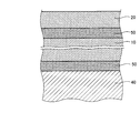
- FIG. 1 is a schematic diagram showing a configuration of a power module that is a laminate according to an embodiment of the present invention.
- FIG. 2 is an enlarged cross-sectional view showing a main part of the laminate shown in FIG.
- FIG. 3 is a schematic diagram showing an outline of the cold spray apparatus.
- FIG. 4 is a schematic diagram showing a configuration of a power module that is a laminated body according to Modification 1 of the embodiment of the present invention.
- FIG. 5 is a diagram for explaining a production process of a laminate according to an example and a comparative example of the present invention.
- FIG. 6 is a graph showing thermal expansion characteristics when a thermal load is applied to the laminates according to examples and comparative examples of the present invention.
- FIG. 1 is a schematic diagram showing a configuration of a power module that is a laminate according to an embodiment of the present invention.
- FIG. 2 is an enlarged cross-sectional view showing a main part of the laminate shown in FIG.
- a power module 1 shown in FIG. 1 includes a ceramic substrate 10 that is an insulating substrate, a circuit layer 20 formed on one surface of the ceramic substrate 10, and a chip 30 that is bonded to the circuit layer 20 by solder C1. And a cooling fin 40 provided on the surface of the ceramic substrate 10 opposite to the circuit layer 20.
- the base material 10 is a substantially plate-like member made of an insulating material.
- the insulating material include nitride ceramics such as aluminum nitride and silicon nitride, oxide ceramics such as alumina, magnesia, zirconia, steatite, forsterite, mullite, titania, silica, and sialon, and inorganic filler.
- a blended resin layer or the like is used.
- the circuit layer 20 is a metal film layer formed by a cold spray method to be described later, and is made of copper having a hydrogen content of 0.002% by mass or less.
- the circuit layer 20 is formed with a circuit pattern for transmitting an electrical signal to the chip 30 and the like.
- the chip 30 is realized by a semiconductor element such as a diode, a transistor, or an IGBT (insulated gate bipolar transistor). A plurality of chips 30 may be provided on the substrate 10 in accordance with the purpose of use.
- the cooling fin 40 is made of a metal or alloy having good thermal conductivity such as copper, copper alloy, aluminum, aluminum alloy, silver, silver alloy, etc., and is manufactured by casting, machining, etc. Those formed by the method can also be used. The heat generated from the chip 30 is released to the outside through the substrate 10 through the cooling fin 40.
- an intermediate layer 50 mainly composed of a metal or an alloy is provided between the base material 10 and the circuit layer 20 and between the base material 10 and the cooling fin 40.
- the intermediate layer 50 is formed by bonding a plate-like metal or alloy member (hereinafter collectively referred to as a metal member) to the base material 10 using a brazing material.
- the type of brazing material can be selected according to the type of base material 10 and the type of plate-like metal member.
- aluminum is the main component
- silver is the main component
- at least one of copper and tin is contained.
- a silver brazing material containing titanium which is an active metal can be used.
- the plate-like metal member a metal or alloy having a hardness that can be joined to the base material 10 by brazing and can form a film by a cold spray method is used. Since the hardness range varies depending on the film forming conditions in the cold spray method and the like, it is not unconditionally determined, but in general, any metal member having a Vickers hardness of 100 HV or less can be applied. Specific examples include aluminum, silver, gold, copper, and alloys containing these metals.
- the circuit layer 20 formed on the surface of the intermediate layer 50 is made of copper containing 0.002% by mass or less of hydrogen.
- the circuit layer 20 may be formed using copper powder having a hydrogen content of 0.002% by mass or less.
- the copper powder having a hydrogen content of 0.002% by mass or less may be powdered by an atomizing method, preferably a water atomizing method, and not subjected to a reduction heat treatment in a hydrogen atmosphere.
- copper powder produced by the atomization method is widely used as a conductive material because the impurity concentration in the obtained powder can be reduced as compared with the wet reduction method.
- the copper powder used as the conductive material is subjected to a reduction heat treatment in a hydrogen atmosphere, and the electrical conductivity is further improved by reducing the amount of oxygen contained in the powder.
- a circuit layer 20 as a metal film is formed on the substrate 10 via the intermediate layer 50 by a cold spray method, and a thermal load is applied by connecting the chip 30 with the solder C1.
- the circuit layer 20 may be peeled off from the base material 10, the base material 10 may be cracked, or a metal film (circuit layer 20) void may be generated.
- the specific thermal expansion of the circuit layer 20 that is a metal film layer is generated by heat, and the specific thermal expansion of the circuit layer 20 is It has been found that the hydrogen in the powder increased by the reduction heat treatment in the hydrogen atmosphere of the copper powder is caused when it is volatilized from the circuit layer 20 by heat.
- the circuit layer 20 since the circuit layer 20 is formed using copper powder that is not subjected to reductive heat treatment in a hydrogen atmosphere, the circuit layer 20 is peeled off from the base material 10 due to a thermal load, or the base material 10 is cracked. Generation of voids in the metal film (circuit layer 20) can be prevented.
- the circuit layer 20 is formed at a low temperature by the cold spray method, the influence of thermal stress is alleviated. Therefore, it is possible to obtain a metal film having no phase transformation and suppressing oxidation.
- plastic deformation occurs between the copper powder and the metal or alloy member that is the material of the intermediate layer 50, thereby obtaining an anchor effect and destroying each other's oxide film. As a result, metal bonding occurs between the new surfaces, so that a laminate with high adhesion strength can be obtained.
- the oxygen content of the copper powder forming the circuit layer 20 is preferably 0.03% by mass or more and 0.15% by mass or less.
- the oxygen content of the copper powder is within the above range, the electrical conductivity of the circuit layer 20 is improved, and the specific expansion of the circuit layer 20 due to a thermal load can be prevented.
- the copper powder is preferably heat-treated in a vacuum atmosphere.
- the heat treatment is preferably performed at 400 ° C. to 800 ° C. for about 1 to 2 hours.
- the oxygen content of a copper powder can be reduced by performing an atomization process etc. in a vacuum melting furnace.
- the copper powder used in this embodiment is preferably one that is not subjected to a reduction heat treatment in a hydrogen atmosphere, but the copper powder that has been subjected to a reduction heat treatment in a hydrogen atmosphere is heat-treated in a vacuum atmosphere to produce hydrogen.
- a copper powder having a content of 0.002% by mass or less and an oxygen content of 0.03% by mass to 0.07% by mass may be used.
- phosphorus or phosphorus copper ingot may be added to molten copper for the purpose of improving the fluidity of the molten metal and deoxidizing.
- the amount of oxygen contained can be reduced and the melt fluidity can be improved by the addition of phosphorus, the residual elongation after heat load increases as the amount of phosphorus added increases. Therefore, when adding phosphorus to copper powder, it is preferable that phosphorus content in copper powder shall be 0.002 mass% or more and 0.028 mass% or less.
- the circuit layer 20 having excellent properties can be obtained.
- the phosphorus content in the copper powder is particularly preferably 0.005% by mass or more and 0.018% by mass or less.
- Copper powder having an average particle diameter of 5 ⁇ m to 80 ⁇ m can be used.
- An average particle diameter of 20 ⁇ m to 50 ⁇ m is particularly preferable from the viewpoints of handleability and the denseness of the circuit layer 20.
- FIG. 3 is a schematic diagram showing an outline of the cold spray apparatus.
- the base material 10 having the intermediate layer 50 formed on the surface is prepared.
- an aluminum (Al) brazing material and a metal foil such as aluminum (Al) are disposed on the surface of the base material 10, or a silver brazing material and a metal foil such as copper are placed in a vacuum. It can be formed by heat treatment.
- the cold spray device 60 contains a gas heater 61 that heats the compressed gas, a powder supply device 62 that contains the copper powder of the material of the circuit layer 20 and supplies it to the spray gun 63, and the heated compressed gas and the supply thereof
- a gas nozzle 64 for injecting the material powder applied onto the substrate, and valves 65 and 66 for adjusting the amount of compressed gas supplied to the gas heater 61 and the powder supply device 62 are provided.
- the compressed gas helium, nitrogen, air or the like is used.
- the compressed gas supplied to the gas heater 61 is, for example, 50 ° C. or higher, heated to a temperature in a range lower than the melting point of the copper powder that is the material of the circuit layer 20, and then supplied to the spray gun 63. .
- the heating temperature of the compressed gas is preferably 300 to 900 ° C.
- the compressed gas supplied to the powder supply device 62 supplies the copper powder in the powder supply device 62 to the spray gun 63 so as to have a predetermined discharge amount.
- the heated compressed gas is made a supersonic flow (about 340 m / s or more) by the gas nozzle 64 having a divergent shape.
- the gas pressure of the compressed gas is preferably about 1 to 5 MPa. This is because the adhesion strength of the circuit layer 20 to the intermediate layer 50 can be improved by adjusting the pressure of the compressed gas to this level. More preferably, the treatment is performed at a pressure of about 2 to 4 MPa.
- the copper powder supplied to the spray gun 63 is accelerated by the injection of the compressed gas into the supersonic flow, and collides and deposits at a high speed on the intermediate layer 50 on the base material 10 in the solid state. Form a metal film. Note that the apparatus is not limited to the cold spray apparatus 60 shown in FIG.
- the circuit layer 20 may be formed by disposing a metal mask having a circuit pattern formed on the intermediate layer 50 and forming a film.
- the cooling fin 40 is cut into a desired shape and bonded to the surface of the substrate 10 opposite to the surface on which the circuit layer 20 is formed with a heat transfer sheet or grease, for example, using aluminum powder.
- a film (deposition layer) having a desired thickness may be formed by the cold spray device 60, and then a desired flow path pattern may be formed by laser cutting or the like on the film (deposition layer).
- the circuit layer 20 is produced by the cold spray method using the copper powder having a hydrogen content of 0.002% by mass or less, so that it is specific even when a heat load is applied. It is possible to obtain the power module 1 that is free from problems such as cracking of the base material 10 due to thermal expansion and that does not have voids in the circuit layer 20. Moreover, since the circuit layer 20 is formed on the surface of the base material 10 via the intermediate layer 50, the circuit layer 20 having excellent adhesion can be obtained.
- FIG. 4 is a schematic diagram showing a configuration of a power module according to Modification 1 of the embodiment of the present invention.
- a power module 1A according to Modification 1 shown in FIG. 4 includes a base material 10, an intermediate layer 50A formed on one surface of the base material 10, and an intermediate layer 50A ′ formed on the other surface of the base material 10.
- a buffer layer 60 formed on the surface of the intermediate layer 50A ′, a heat diffusion layer 70 formed on the surface of the intermediate layer 50A, a chip 30 disposed on the heat diffusion layer 70 via the solder C1,
- the buffer layer 60 includes cooling fins 40 disposed via a heat transfer sheet (not shown).
- the intermediate layer 50A is made of a metal having good electrical conductivity, such as copper, and is joined to the base material 10 via a brazing material.
- the intermediate layer 50A also functions as a circuit layer, and the circuit pattern of the intermediate layer 50A is formed by etching or the like.
- the intermediate layer 50 ⁇ / b> A ′ is made of a metal having good electrical conductivity, such as copper, and is bonded to the base material 10 via a brazing material.
- the intermediate layer 50 ⁇ / b> A ′ transfers heat generated in the chip 30 and the intermediate layer 50 ⁇ / b> A to the buffer layer 60 and the cooling fin 40.
- the thermal diffusion layer 70 is a metal film directly formed on the intermediate layer 50A by a cold spray method using copper powder having a hydrogen content of 0.002% by mass or less.
- the thermal diffusion layer 70 can reduce the thermal resistance by diffusing the heat generated in the chip 30 not only in the thickness direction of the substrate 10 but also in a plane orthogonal to the thickness direction.
- the buffer layer 60 is formed of a material having a high thermal conductivity and a thermal expansion coefficient that is an intermediate between the materials used for the base material 10 and the cooling fins 40.
- a composite material containing copper and any metal of iron-nickel alloy, titanium, chromium, tungsten, and molybdenum (hereinafter also referred to as an additive), aluminum, copper, nickel, iron-nickel alloy, titanium, It is a composite material containing any one metal of chromium, tungsten and molybdenum (hereinafter also referred to as an additive), and is directly formed on the surface of the intermediate layer 50A ′ by a cold spray method.
- the buffer layer 60 has good heat conductivity for efficiently conducting the heat generated in the chip 30 and the intermediate layer 50A to the cooling fin 40, and a low coefficient of thermal expansion for alleviating the thermal stress in the base material 10. ing.
- the thermal conductivity in the buffer layer 60 is preferably 75 W / mK or more and 220 W / mK or less, and the coefficient of thermal expansion (CTE) is 7.1 ⁇ 10 ⁇ 6 / K or more and 11 ⁇ 10 ⁇ 6 / It is preferable that it is K or less.
- the thickness of the heat diffusion layer 70 depends on the area of the region where the chip 30 is mounted, but is preferably about 0.5 mm to 1.5 mm. In relation to the buffer layer 60, the thickness of the thermal diffusion layer 70 may be set to be not less than 1/2 times and not more than 1 time the thickness of the buffer layer 60.
- the thermal diffusion layer 70 is cold-sprayed by using a copper powder having a hydrogen content of 0.002% by mass or less between the intermediate layer 50A and the chip 30. Since the thermal resistance in the intermediate layer 50A and the base material 10 is reduced, the thermal stress applied to the base material 10 can be relaxed. Further, since the buffer layer 60 is formed on the surface of the intermediate layer 50A ′ by the cold spray method, the thermal stress applied to the base material 10 can be further relaxed. Furthermore, by adjusting the material constituting the buffer layer 60, good heat transfer in the buffer layer 60 can be maintained. Therefore, the heat generated in the chip 30 and the intermediate layer 50A can be efficiently released to the outside through the cooling fins 40, and the power module 1A having excellent durability can be realized.
- the power module has been described as an example.
- the embodiment of the present invention can also be applied to the case where a metal film is directly formed on a base material made of a metal or an alloy. Copper powder with a hydrogen content of 0.002% by mass or less is accelerated together with gas on a base material made of metal or an alloy, and is sprayed and deposited on the surface of the base material in a solid state.
- the laminate in which the metal film is formed has a small hydrogen content in the copper powder constituting the metal film, so that the metal film has few voids and is excellent in thermal conductivity, conductivity and strength.
- middle layer on both surfaces of the base material which consists of silicon nitride through the brazing material was used.
- Example 1 A metal film was formed on an AMC substrate (insulating base material: silicon nitride (thickness 0.32 mm), intermediate layer: pure copper (thickness 0.5 mm)) by the process shown as Example 1 in FIG.
- the copper powder is obtained by melting copper to form a molten metal and then heat-treating it at 600 ° C. for 2 hours in a vacuum atmosphere by using a water atomizing method to obtain a copper powder having an average particle size of about 35 ⁇ m.
- the hydrogen content of this copper powder is 0.002 mass% or less.
- the metal film was prepared by using the prepared copper powder with a cold spray device 60, working gas: nitrogen, working gas temperature: 800 ° C., working gas pressure: 3 MPa, working distance (WD): 25 mm, traverse speed: 200 mm / s, pass Number of times: It was made by spraying on an AMC substrate at one time.
- Example 2 A metal film was formed on an AMC substrate (insulating base material: silicon nitride (thickness 0.32 mm), intermediate layer: pure copper (thickness 0.5 mm)) by the process shown as Example 2 in FIG.
- the copper powder is obtained by melting copper to form a molten metal and then making a copper powder having an average particle diameter of about 35 ⁇ m by a water atomization method.
- the hydrogen content of this copper powder is 0.002 mass% or less.
- the spraying conditions by the cold spray device 60 for the metal film are the same as in the first embodiment.
- Example 3 A metal film was formed on the AMC substrate (insulating base material: silicon nitride (thickness 0.32 mm), intermediate layer: pure copper (thickness 0.5 mm)) by the process shown as Example 3 in FIG.
- the copper powder is obtained by melting copper to form a molten metal, and then adding phosphorus to 0.006% by mass, making the copper powder having an average particle diameter of about 35 ⁇ m by a water atomization method, and at 600 ° C. under vacuum atmosphere at 2 ° C. Heat-treated for hours.
- the hydrogen content of this copper powder is 0.002 mass% or less.
- the spraying conditions by the cold spray device 60 for the metal film are the same as in the first embodiment.
- Example 4 A metal film was formed on an AMC substrate (insulating base material: silicon nitride (thickness 0.32 mm), intermediate layer: pure copper (thickness 0.5 mm)) by the process shown as Example 4 in FIG.
- the copper powder is obtained by melting copper to form a molten metal, and then adding phosphorus in an amount of 0.006% by mass to obtain a copper powder having an average particle diameter of about 35 ⁇ m by a water atomization method.
- the hydrogen content of this copper powder is 0.002 mass% or less.
- the spraying conditions by the cold spray device 60 for the metal film are the same as in the first embodiment.
- Comparative Example 1 A metal film was formed on an AMC substrate (insulating base material: silicon nitride (thickness 0.32 mm), intermediate layer: pure copper (thickness 0.5 mm)) by the process shown as Comparative Example 1 in FIG.
- the copper powder is prepared by melting copper to form a molten metal, and then adding phosphorus to 0.01% by mass, forming a copper powder having an average particle size of about 35 ⁇ m by a water atomization method, and at 400 ° C. under a hydrogen atmosphere at 1 ° C. Time-reduced heat treatment.
- the copper powder has a hydrogen content of 0.01% by mass and an oxygen content of 0.07% by mass.
- the spraying conditions by the cold spray device 60 for the metal film are the same as in the first embodiment.
- Comparative Example 2 A metal film was formed on an AMC substrate (insulating base material: silicon nitride (thickness 0.32 mm), intermediate layer: pure copper (thickness 0.5 mm)) by the process shown as Comparative Example 2 in FIG.
- the copper powder was made by melting copper to form a molten metal, and then adding copper powder with an average particle diameter of about 35 ⁇ m by a water atomization method without adding phosphorus, and after reducing heat treatment at 400 ° C. for 1 hour in a hydrogen atmosphere, The heat treatment is performed by reducing heat treatment at 700 ° C. for 1 hour.
- the copper powder has a hydrogen content of 0.005% by mass and an oxygen content of 0.07% by mass.
- the spraying conditions by the cold spray device 60 for the metal film are the same as in the first embodiment.
- Comparative Example 3 A metal film was formed on an AMC substrate (insulating base material: silicon nitride (thickness 0.32 mm), intermediate layer: pure copper (thickness 0.5 mm)) by the process shown as Comparative Example 3 in FIG.
- the copper powder is prepared by melting copper to form a molten metal, and then adding phosphorus to 0.01% by mass, forming a copper powder having an average particle size of about 35 ⁇ m by a water atomization method, and at 400 ° C. under a hydrogen atmosphere at 1 ° C. Time-reduced heat treatment.
- the copper powder has a hydrogen content of 0.01% by mass and an oxygen content of 0.07% by mass.
- Comparative Example 3 after using this copper powder to form a metal film with the cold spray device 60 in the same manner as in Example 1, it was heat-treated in a vacuum atmosphere at 600 ° C. for 2 hours.
- Comparative Example 4 A metal film was formed on an AMC substrate (insulating base material: silicon nitride (thickness 0.32 mm), intermediate layer: pure copper (thickness 0.5 mm)) by the process shown as Comparative Example 4 in FIG.
- the copper powder is made by melting copper to form a molten metal, and then adding copper powder with an average particle size of about 35 ⁇ m by a water atomizing method without adding phosphorus, after reducing heat treatment at 400 ° C. for 1 hour in a hydrogen atmosphere, and further adding 700 The heat treatment is performed by reducing heat treatment at 1 ° C. for 1 hour.
- the copper powder has a hydrogen content of 0.005% by mass and an oxygen content of 0.07% by mass.
- heat treatment was performed at 600 ° C. for 2 hours in a vacuum atmosphere.
- Comparative Example 5 A metal film was formed on the AMC substrate (insulating base material: silicon nitride (thickness 0.32 mm), intermediate layer: pure copper (thickness 0.5 mm)) by the process shown as Comparative Example 5 in FIG.
- the copper powder is obtained by melting copper to form a molten metal, and then adding phosphorus in an amount of 0.01% by mass to obtain a copper powder having an average particle size of about 35 ⁇ m by a water atomization method.
- the copper powder has a hydrogen content of 0.001% by mass and an oxygen content of 0.14% by mass.
- heat treatment was performed at 600 ° C. for 2 hours in a vacuum atmosphere.
- Comparative Example 6 A metal film was formed on an AMC substrate (insulating base material: silicon nitride (thickness 0.32 mm), intermediate layer: pure copper (thickness 0.5 mm)) by the process shown as Comparative Example 6 in FIG.
- the copper powder is obtained by melting copper to form a molten metal, and then adding copper to an average particle diameter of about 35 ⁇ m by a water atomization method without adding phosphorus.
- the copper powder has a hydrogen content of 0.001% by mass and an oxygen content of 0.15% by mass.
- Comparative Example 6 after using this copper powder to form a metal film with the cold spray device 60 in the same manner as in Example 1, it was heat-treated in a vacuum atmosphere at 600 ° C. for 2 hours.
- Table 1 summarizes the characteristics of the metal film in the laminates of Examples 1 to 4 and Comparative Examples 1 to 6, and the thermal expansion / shrinkage characteristics of the metal film after heat treatment, voids, cracks in the substrate, peeling of the film, etc. It was.
- FIG. 6 shows the correlation between the time during heat treatment and the elongation of the metal film (TMA) for the laminates of Examples 1 to 4 and Comparative Example 1.
- the left scale is the elongation of the metal film (TMA, ⁇ m)
- the right scale is the temperature (° C.)
- the solid line shown in the graph is the heat treatment condition.
- the temperature was increased to 800 ° C. at 10 ° C./minute, held at 800 ° C.
- TMA cut out the metal film of 5 mm x 5 mm x 15 mm from the laminated body, and measured with RIGAKU TMA measuring apparatus ThermoPlusTG8120.
- a metal film was formed from Examples 1 to 4, Comparative Examples 5 and 6 that were not subjected to reduction heat treatment in a hydrogen atmosphere, and copper powder that was subjected to reduction heat treatment in a hydrogen atmosphere.
- Comparative Examples 3 and 4 where heat treatment was performed in a vacuum atmosphere the amount of hydrogen in the metal film was low.
- Examples 1 to 4 have a low amount of hydrogen in the metal film, so there is no specific thermal expansion / shrinkage, and no peeling of the metal film or cracking of the substrate occurs.
- Examples 1 and 2 where phosphorus is not added there are almost no voids in the metal film, and in Examples 3 and 4 where phosphorus is added, a small amount of voids are generated, and the thermal expansion of the metal film is larger than in Examples 1 and 2, The residual elongation increased even after cooling.
- a metal film is formed with copper powder that has been subjected to a reduction heat treatment in a hydrogen atmosphere.
- the heat treatment is performed in a vacuum atmosphere after the metal film is formed, the amount of hydrogen in the metal film is small. A lot of voids are generated when hydrogen is released from the metal film by the heat treatment after the film, and the heat treatment is performed after forming the laminated body, so that the base material is easily cracked.
- the laminated body and the method for producing the laminated body according to the present invention are useful for obtaining a laminated body that is free from cracking of the insulating base material and has no metal film voids.
Landscapes
- Chemical & Material Sciences (AREA)
- Engineering & Computer Science (AREA)
- Materials Engineering (AREA)
- Organic Chemistry (AREA)
- Mechanical Engineering (AREA)
- Metallurgy (AREA)
- Chemical Kinetics & Catalysis (AREA)
- Ceramic Engineering (AREA)
- Physics & Mathematics (AREA)
- Thermal Sciences (AREA)
- Microelectronics & Electronic Packaging (AREA)
- Condensed Matter Physics & Semiconductors (AREA)
- Computer Hardware Design (AREA)
- Power Engineering (AREA)
- General Physics & Mathematics (AREA)
- Wood Science & Technology (AREA)
- Life Sciences & Earth Sciences (AREA)
- Manufacturing & Machinery (AREA)
- Structural Engineering (AREA)
- Laminated Bodies (AREA)
- Other Surface Treatments For Metallic Materials (AREA)
- Cooling Or The Like Of Semiconductors Or Solid State Devices (AREA)
- Manufacture Of Metal Powder And Suspensions Thereof (AREA)
- Powder Metallurgy (AREA)
Abstract
Description
AMC基板(絶縁基材:窒化ケイ素(厚み0.32mm)、中間層:純銅(厚み0.5mm))に、図5の実施例1として示す工程により金属皮膜を成膜した。銅粉末は、銅を溶融して溶湯とした後、水アトマイズ法により平均粒径:約35μmの銅粉末とし、真空雰囲気下で600℃、2時間熱処理したものである。この銅粉末の水素含有量は0.002質量%以下である。金属皮膜は、調製した銅粉末を、コールドスプレー装置60により、作動ガス:窒素、作動ガス温度:800℃、作動ガス圧力:3MPa、ワーキングディスタンス(WD):25mm、トラバース速度:200mm/s、パス回数:1回で、AMC基板に吹付けて作製した。 Example 1
A metal film was formed on an AMC substrate (insulating base material: silicon nitride (thickness 0.32 mm), intermediate layer: pure copper (thickness 0.5 mm)) by the process shown as Example 1 in FIG. The copper powder is obtained by melting copper to form a molten metal and then heat-treating it at 600 ° C. for 2 hours in a vacuum atmosphere by using a water atomizing method to obtain a copper powder having an average particle size of about 35 μm. The hydrogen content of this copper powder is 0.002 mass% or less. The metal film was prepared by using the prepared copper powder with a
AMC基板(絶縁基材:窒化ケイ素(厚み0.32mm)、中間層:純銅(厚み0.5mm))に、図5の実施例2として示す工程により金属皮膜を成膜した。銅粉末は、銅を溶融して溶湯とした後、水アトマイズ法により平均粒径:約35μmの銅粉末としたものである。この銅粉末の水素含有量は0.002質量%以下である。金属皮膜のコールドスプレー装置60による吹付条件は実施例1と同様である。 (Example 2)
A metal film was formed on an AMC substrate (insulating base material: silicon nitride (thickness 0.32 mm), intermediate layer: pure copper (thickness 0.5 mm)) by the process shown as Example 2 in FIG. The copper powder is obtained by melting copper to form a molten metal and then making a copper powder having an average particle diameter of about 35 μm by a water atomization method. The hydrogen content of this copper powder is 0.002 mass% or less. The spraying conditions by the
AMC基板(絶縁基材:窒化ケイ素(厚み0.32mm)、中間層:純銅(厚み0.5mm))に、図5の実施例3として示す工程により金属皮膜を成膜した。銅粉末は、銅を溶融して溶湯とした後、リンを0.006質量%となるよう添加し、水アトマイズ法により平均粒径:約35μmの銅粉末とし、真空雰囲気下で600℃、2時間熱処理したものである。この銅粉末の水素含有量は0.002質量%以下である。金属皮膜のコールドスプレー装置60による吹付条件は実施例1と同様である。 (Example 3)
A metal film was formed on the AMC substrate (insulating base material: silicon nitride (thickness 0.32 mm), intermediate layer: pure copper (thickness 0.5 mm)) by the process shown as Example 3 in FIG. The copper powder is obtained by melting copper to form a molten metal, and then adding phosphorus to 0.006% by mass, making the copper powder having an average particle diameter of about 35 μm by a water atomization method, and at 600 ° C. under vacuum atmosphere at 2 ° C. Heat-treated for hours. The hydrogen content of this copper powder is 0.002 mass% or less. The spraying conditions by the
AMC基板(絶縁基材:窒化ケイ素(厚み0.32mm)、中間層:純銅(厚み0.5mm))に、図5の実施例4として示す工程により金属皮膜を成膜した。銅粉末は、銅を溶融して溶湯とした後、リンを0.006質量%となるよう添加し、水アトマイズ法により平均粒径:約35μmの銅粉末としたものである。この銅粉末の水素含有量は0.002質量%以下である。金属皮膜のコールドスプレー装置60による吹付条件は実施例1と同様である。 Example 4
A metal film was formed on an AMC substrate (insulating base material: silicon nitride (thickness 0.32 mm), intermediate layer: pure copper (thickness 0.5 mm)) by the process shown as Example 4 in FIG. The copper powder is obtained by melting copper to form a molten metal, and then adding phosphorus in an amount of 0.006% by mass to obtain a copper powder having an average particle diameter of about 35 μm by a water atomization method. The hydrogen content of this copper powder is 0.002 mass% or less. The spraying conditions by the
AMC基板(絶縁基材:窒化ケイ素(厚み0.32mm)、中間層:純銅(厚み0.5mm))に、図5の比較例1として示す工程により金属皮膜を成膜した。銅粉末は、銅を溶融して溶湯とした後、リンを0.01質量%となるよう添加し、水アトマイズ法により平均粒径:約35μmの銅粉末とし、水素雰囲気下で400℃、1時間還元熱処理したものである。この銅粉末の水素含有量は0.01質量%であり、酸素含有量は0.07質量%である。金属皮膜のコールドスプレー装置60による吹付条件は実施例1と同様である。 (Comparative Example 1)
A metal film was formed on an AMC substrate (insulating base material: silicon nitride (thickness 0.32 mm), intermediate layer: pure copper (thickness 0.5 mm)) by the process shown as Comparative Example 1 in FIG. The copper powder is prepared by melting copper to form a molten metal, and then adding phosphorus to 0.01% by mass, forming a copper powder having an average particle size of about 35 μm by a water atomization method, and at 400 ° C. under a hydrogen atmosphere at 1 ° C. Time-reduced heat treatment. The copper powder has a hydrogen content of 0.01% by mass and an oxygen content of 0.07% by mass. The spraying conditions by the
AMC基板(絶縁基材:窒化ケイ素(厚み0.32mm)、中間層:純銅(厚み0.5mm))に、図5の比較例2として示す工程により金属皮膜を成膜した。銅粉末は、銅を溶融して溶湯とした後、リンを添加しないで水アトマイズ法により平均粒径:約35μmの銅粉末とし、水素雰囲気下で400℃、1時間還元熱処理した後、さらに、700℃、1時間還元熱処理したものである。この銅粉末の水素含有量は0.005質量%であり、酸素含有量は0.07質量%である。金属皮膜のコールドスプレー装置60による吹付条件は実施例1と同様である。 (Comparative Example 2)
A metal film was formed on an AMC substrate (insulating base material: silicon nitride (thickness 0.32 mm), intermediate layer: pure copper (thickness 0.5 mm)) by the process shown as Comparative Example 2 in FIG. The copper powder was made by melting copper to form a molten metal, and then adding copper powder with an average particle diameter of about 35 μm by a water atomization method without adding phosphorus, and after reducing heat treatment at 400 ° C. for 1 hour in a hydrogen atmosphere, The heat treatment is performed by reducing heat treatment at 700 ° C. for 1 hour. The copper powder has a hydrogen content of 0.005% by mass and an oxygen content of 0.07% by mass. The spraying conditions by the
AMC基板(絶縁基材:窒化ケイ素(厚み0.32mm)、中間層:純銅(厚み0.5mm))に、図5の比較例3として示す工程により金属皮膜を成膜した。銅粉末は、銅を溶融して溶湯とした後、リンを0.01質量%となるよう添加し、水アトマイズ法により平均粒径:約35μmの銅粉末とし、水素雰囲気下で400℃、1時間還元熱処理したものである。この銅粉末の水素含有量は0.01質量%であり、酸素含有量は0.07質量%である。比較例3では、この銅粉末を用いて、実施例1と同様にしてコールドスプレー装置60にて金属皮膜を成膜した後、真空雰囲気下で600℃、2時間熱処理した。 (Comparative Example 3)
A metal film was formed on an AMC substrate (insulating base material: silicon nitride (thickness 0.32 mm), intermediate layer: pure copper (thickness 0.5 mm)) by the process shown as Comparative Example 3 in FIG. The copper powder is prepared by melting copper to form a molten metal, and then adding phosphorus to 0.01% by mass, forming a copper powder having an average particle size of about 35 μm by a water atomization method, and at 400 ° C. under a hydrogen atmosphere at 1 ° C. Time-reduced heat treatment. The copper powder has a hydrogen content of 0.01% by mass and an oxygen content of 0.07% by mass. In Comparative Example 3, after using this copper powder to form a metal film with the
AMC基板(絶縁基材:窒化ケイ素(厚み0.32mm)、中間層:純銅(厚み0.5mm))に、図5の比較例4として示す工程により金属皮膜を成膜した。銅粉末は、銅を溶融して溶湯とした後、リンを添加しないで水アトマイズ法により平均粒径:約35μmの銅粉末とし、水素雰囲気下400℃、1時間還元熱処理した後、さらに、700℃、1時間還元熱処理したものである。この銅粉末の水素含有量は0.005質量%であり、酸素含有量は0.07質量%である。比較例4では、この銅粉末を用いて、実施例1と同様にしてコールドスプレー装置60にて金属皮膜を成膜した後、真空雰囲気下で600℃、2時間熱処理した。 (Comparative Example 4)
A metal film was formed on an AMC substrate (insulating base material: silicon nitride (thickness 0.32 mm), intermediate layer: pure copper (thickness 0.5 mm)) by the process shown as Comparative Example 4 in FIG. The copper powder is made by melting copper to form a molten metal, and then adding copper powder with an average particle size of about 35 μm by a water atomizing method without adding phosphorus, after reducing heat treatment at 400 ° C. for 1 hour in a hydrogen atmosphere, and further adding 700 The heat treatment is performed by reducing heat treatment at 1 ° C. for 1 hour. The copper powder has a hydrogen content of 0.005% by mass and an oxygen content of 0.07% by mass. In Comparative Example 4, after using this copper powder to form a metal film in the
AMC基板(絶縁基材:窒化ケイ素(厚み0.32mm)、中間層:純銅(厚み0.5mm))に、図5の比較例5として示す工程により金属皮膜を成膜した。銅粉末は、銅を溶融して溶湯とした後、リンを0.01質量%となるよう添加し、水アトマイズ法により平均粒径:約35μmの銅粉末としたものである。この銅粉末の水素含有量は0.001質量%であり、酸素含有量は0.14質量%である。比較例5では、この銅粉末を用いて、実施例1と同様にしてコールドスプレー装置60にて金属皮膜を成膜した後、真空雰囲気下で600℃、2時間熱処理した。 (Comparative Example 5)
A metal film was formed on the AMC substrate (insulating base material: silicon nitride (thickness 0.32 mm), intermediate layer: pure copper (thickness 0.5 mm)) by the process shown as Comparative Example 5 in FIG. The copper powder is obtained by melting copper to form a molten metal, and then adding phosphorus in an amount of 0.01% by mass to obtain a copper powder having an average particle size of about 35 μm by a water atomization method. The copper powder has a hydrogen content of 0.001% by mass and an oxygen content of 0.14% by mass. In Comparative Example 5, after using this copper powder to form a metal film with the
AMC基板(絶縁基材:窒化ケイ素(厚み0.32mm)、中間層:純銅(厚み0.5mm))に、図5の比較例6として示す工程により金属皮膜を成膜した。銅粉末は、銅を溶融して溶湯とした後、リンを添加せずに水アトマイズ法により平均粒径:約35μmの銅粉末としたものである。この銅粉末の水素含有量は0.001質量%であり、酸素含有量は0.15質量%である。比較例6では、この銅粉末を用いて、実施例1と同様にしてコールドスプレー装置60にて金属皮膜を成膜した後、真空雰囲気下で600℃、2時間熱処理した。 (Comparative Example 6)
A metal film was formed on an AMC substrate (insulating base material: silicon nitride (thickness 0.32 mm), intermediate layer: pure copper (thickness 0.5 mm)) by the process shown as Comparative Example 6 in FIG. The copper powder is obtained by melting copper to form a molten metal, and then adding copper to an average particle diameter of about 35 μm by a water atomization method without adding phosphorus. The copper powder has a hydrogen content of 0.001% by mass and an oxygen content of 0.15% by mass. In Comparative Example 6, after using this copper powder to form a metal film with the

10 基材
20 回路層
30 チップ
40 冷却フィン
50、50A、50A’ 中間層
60 緩衝層
70 熱拡散層
60 コールドスプレー装置
61 ガス加熱器
62 粉末供給装置
63 スプレーガン
64 ガスノズル
65、66 バルブ DESCRIPTION OF
Claims (12)
- 絶縁性を有する基材と、
前記基材の表面に形成された金属又は合金を主成分とする中間層と、
含有する水素量が0.002質量%以下の銅粉末からなり、前記中間層上に積層されてなる金属皮膜と、
を備え、前記中間層と前記金属皮膜との界面が塑性変形していることを特徴とする積層体。 A base material having insulating properties;
An intermediate layer mainly composed of metal or alloy formed on the surface of the substrate;
A metal film made of copper powder having a hydrogen content of 0.002% by mass or less and laminated on the intermediate layer;
And the interface between the intermediate layer and the metal coating is plastically deformed. - 金属または合金からなる基材と、
含有する水素量が0.002質量%以下の銅粉末からなり、前記基材上に積層されてなる金属皮膜と、
を備え、前記基材と前記金属皮膜との界面が塑性変形していることを特徴とする積層体。 A base material made of metal or alloy;
A metal film comprising a copper powder having a hydrogen content of 0.002% by mass or less and laminated on the substrate;
And a laminate in which the interface between the base material and the metal film is plastically deformed. - 前記銅粉末の酸素含有量は、0.03質量%以上0.15質量%以下であることを特徴とする請求項1または2に記載の積層体。 The laminate according to claim 1 or 2, wherein the copper powder has an oxygen content of 0.03 mass% or more and 0.15 mass% or less.
- 前記銅粉末のリン含有量は、0.002質量%以上0.028質量%以下であることを特徴とする請求項1~3のいずれか一つに記載の積層体。 The laminated body according to any one of claims 1 to 3, wherein the copper powder has a phosphorus content of 0.002 mass% or more and 0.028 mass% or less.
- 金属又は合金を主成分とする中間層が形成された絶縁性を有する基材の表面に、含有する水素量が0.002質量%以下の銅粉末をガスと共に加速し、前記中間層の表面に固相状態のままで吹き付けて堆積させることによって金属皮膜層を形成する皮膜形成工程、を含むことを特徴とする積層体の製造方法。 On the surface of the insulating base material on which an intermediate layer mainly composed of a metal or an alloy is formed, copper powder having a hydrogen content of 0.002% by mass or less is accelerated together with a gas to form a surface on the surface of the intermediate layer. A film forming step of forming a metal film layer by spraying and depositing in a solid state, and producing a laminate.
- 金属又は合金からなる基材の表面に、含有する水素量が0.002質量%以下の銅粉末をガスと共に加速し、前記基材の表面に固相状態のままで吹き付けて堆積させることによって金属皮膜層を形成する皮膜形成工程、を含むことを特徴とする積層体の製造方法。 By accelerating a copper powder having a hydrogen content of 0.002% by mass or less together with a gas on the surface of a base material made of metal or an alloy and spraying and depositing it on the surface of the base material in a solid state, the metal The manufacturing method of the laminated body characterized by including the film formation process which forms a film layer.
- 前記銅粉末の酸素含有量は、0.03質量%以上0.07質量%以下であることを特徴とする請求項5または6に記載の積層体の製造方法。 The method for producing a laminate according to claim 5 or 6, wherein the oxygen content of the copper powder is 0.03 mass% or more and 0.07 mass% or less.
- 溶融した銅に、0.002質量%以上0.028質量%以下の割合でリンまたはリン銅地金を添加し、アトマイズして銅粉末を形成する銅粉末形成工程を含むことを特徴とする請求項5~7のいずれか一つに記載の積層体の製造方法。 Claims characterized by comprising a copper powder forming step of adding phosphorus or phosphorous copper ingot to molten copper at a ratio of 0.002 mass% or more and 0.028 mass% or less, and atomizing to form copper powder. Item 8. The method for producing a laminate according to any one of Items 5 to 7.
- 前記銅粉末形成工程は、銅粉末の水素雰囲気下での還元熱処理を含まないことを特徴とする請求項8に記載の積層体の製造方法。 The method for producing a laminate according to claim 8, wherein the copper powder forming step does not include a reduction heat treatment of the copper powder in a hydrogen atmosphere.
- 前記銅粉末形成工程は、水アトマイズ法により銅粉末を形成することを特徴とする請求項8または9に記載の積層体の製造方法。 The method for producing a laminate according to claim 8 or 9, wherein the copper powder forming step forms a copper powder by a water atomization method.
- 前記銅粉末形成工程は、紛体化した銅粉末を真空雰囲気下で熱処理することを特徴とする請求項8~10のいずれか一つに記載の積層体の製造方法。 The method for producing a laminate according to any one of claims 8 to 10, wherein in the copper powder forming step, the powdered copper powder is heat-treated in a vacuum atmosphere.
- 前記中間層は、板状の金属又は合金部材を前記基材にろう付することにより形成されていることを特徴とする請求項5、7~11のいずれか一つに記載の積層体の製造方法。 The laminate according to any one of claims 5 and 7 to 11, wherein the intermediate layer is formed by brazing a plate-like metal or alloy member to the substrate. Method.
Priority Applications (5)
| Application Number | Priority Date | Filing Date | Title |
|---|---|---|---|
| EP16864329.4A EP3375606B1 (en) | 2015-11-11 | 2016-11-10 | Laminate and laminate manufacturing method |
| US15/774,087 US20180315680A1 (en) | 2015-11-11 | 2016-11-10 | Laminate and method of manufacturing laminate |
| JP2017550402A JP6811719B2 (en) | 2015-11-11 | 2016-11-10 | Method of manufacturing a laminate |
| KR1020187010989A KR102084339B1 (en) | 2015-11-11 | 2016-11-10 | Laminate and Method of Manufacturing the Laminate |
| CN201680064929.8A CN108290380B (en) | 2015-11-11 | 2016-11-10 | Laminate and method for producing laminate |
Applications Claiming Priority (2)
| Application Number | Priority Date | Filing Date | Title |
|---|---|---|---|
| JP2015221265 | 2015-11-11 | ||
| JP2015-221265 | 2015-11-11 |
Publications (1)
| Publication Number | Publication Date |
|---|---|
| WO2017082368A1 true WO2017082368A1 (en) | 2017-05-18 |
Family
ID=58695658
Family Applications (1)
| Application Number | Title | Priority Date | Filing Date |
|---|---|---|---|
| PCT/JP2016/083438 WO2017082368A1 (en) | 2015-11-11 | 2016-11-10 | Laminate and laminate manufacturing method |
Country Status (6)
| Country | Link |
|---|---|
| US (1) | US20180315680A1 (en) |
| EP (1) | EP3375606B1 (en) |
| JP (1) | JP6811719B2 (en) |
| KR (1) | KR102084339B1 (en) |
| CN (1) | CN108290380B (en) |
| WO (1) | WO2017082368A1 (en) |
Cited By (5)
| Publication number | Priority date | Publication date | Assignee | Title |
|---|---|---|---|---|
| JP2019009247A (en) * | 2017-06-23 | 2019-01-17 | フリージア・マクロス株式会社 | Wiring board |
| JP2019033131A (en) * | 2017-08-04 | 2019-02-28 | デンカ株式会社 | Ceramic circuit board |
| JP2019067803A (en) * | 2017-09-28 | 2019-04-25 | デンカ株式会社 | Ceramic circuit board and manufacturing method thereof |
| JP2019067802A (en) * | 2017-09-28 | 2019-04-25 | デンカ株式会社 | Ceramic circuit board and manufacturing method thereof |
| WO2022153891A1 (en) * | 2021-01-12 | 2022-07-21 | デンカ株式会社 | Laminate, method for manufacturing same, and power module |
Families Citing this family (4)
| Publication number | Priority date | Publication date | Assignee | Title |
|---|---|---|---|---|
| WO2018135490A1 (en) * | 2017-01-17 | 2018-07-26 | デンカ株式会社 | Method for producing ceramic circuit board |
| CN110349871A (en) * | 2019-07-10 | 2019-10-18 | 陕西理工大学 | A kind of Cu-Cu direct interconnection method in electronic package |
| GB202000103D0 (en) * | 2020-01-06 | 2020-02-19 | Rolls Royce Plc | Cold spraying |
| CN112157269B (en) * | 2020-09-24 | 2021-11-26 | 四川大学 | Preparation method of cold spray coating based on heat treatment of aluminum alloy powder |
Citations (6)
| Publication number | Priority date | Publication date | Assignee | Title |
|---|---|---|---|---|
| JPS6083399A (en) * | 1983-10-14 | 1985-05-11 | 株式会社日立製作所 | Multilayer printed circuit board and method of producing same |
| JP2010001543A (en) * | 2008-06-23 | 2010-01-07 | Shinko Electric Ind Co Ltd | Method for forming copper film, and wiring board |
| JP2011068942A (en) * | 2009-09-25 | 2011-04-07 | Taiyo Nippon Sanso Corp | Method for forming film |
| JP2012111982A (en) * | 2010-11-19 | 2012-06-14 | Nhk Spring Co Ltd | Laminate and method for producing laminate |
| JP2013018190A (en) * | 2011-07-11 | 2013-01-31 | Nhk Spring Co Ltd | Laminate and method for producing the same |
| JP2015168846A (en) * | 2014-03-06 | 2015-09-28 | 日本発條株式会社 | Laminate and production method of laminate |
Family Cites Families (8)
| Publication number | Priority date | Publication date | Assignee | Title |
|---|---|---|---|---|
| US3931500A (en) | 1973-11-13 | 1976-01-06 | Westinghouse Electric Corporation | System for operating a boiling water reactor steam turbine plant with a combined digital computer and analog control |
| JP4383487B2 (en) * | 2007-03-19 | 2009-12-16 | 古河電気工業株式会社 | Metal-clad laminate and method for producing metal-clad laminate |
| US8394507B2 (en) * | 2009-06-02 | 2013-03-12 | Integran Technologies, Inc. | Metal-clad polymer article |
| JP5504842B2 (en) | 2009-11-20 | 2014-05-28 | 三菱マテリアル株式会社 | Power module substrate, power module substrate with heat sink, power module, and method for manufacturing power module substrate |
| JP5730089B2 (en) * | 2011-03-23 | 2015-06-03 | 日本発條株式会社 | Conductive material, laminate, and method for producing conductive material |
| EP2690678B1 (en) * | 2011-03-25 | 2017-09-13 | NGK Insulators, Ltd. | Layered components and method for producing same |
| JP5745315B2 (en) * | 2011-04-06 | 2015-07-08 | 日本発條株式会社 | LAMINATE AND METHOD FOR PRODUCING LAMINATE |
| JP6621076B2 (en) * | 2013-03-29 | 2019-12-18 | 三菱マテリアル株式会社 | Power module substrate, power module substrate with heat sink, and power module |
-
2016
- 2016-11-10 JP JP2017550402A patent/JP6811719B2/en active Active
- 2016-11-10 WO PCT/JP2016/083438 patent/WO2017082368A1/en active Application Filing
- 2016-11-10 US US15/774,087 patent/US20180315680A1/en not_active Abandoned
- 2016-11-10 EP EP16864329.4A patent/EP3375606B1/en active Active
- 2016-11-10 CN CN201680064929.8A patent/CN108290380B/en active Active
- 2016-11-10 KR KR1020187010989A patent/KR102084339B1/en active IP Right Grant
Patent Citations (6)
| Publication number | Priority date | Publication date | Assignee | Title |
|---|---|---|---|---|
| JPS6083399A (en) * | 1983-10-14 | 1985-05-11 | 株式会社日立製作所 | Multilayer printed circuit board and method of producing same |
| JP2010001543A (en) * | 2008-06-23 | 2010-01-07 | Shinko Electric Ind Co Ltd | Method for forming copper film, and wiring board |
| JP2011068942A (en) * | 2009-09-25 | 2011-04-07 | Taiyo Nippon Sanso Corp | Method for forming film |
| JP2012111982A (en) * | 2010-11-19 | 2012-06-14 | Nhk Spring Co Ltd | Laminate and method for producing laminate |
| JP2013018190A (en) * | 2011-07-11 | 2013-01-31 | Nhk Spring Co Ltd | Laminate and method for producing the same |
| JP2015168846A (en) * | 2014-03-06 | 2015-09-28 | 日本発條株式会社 | Laminate and production method of laminate |
Non-Patent Citations (1)
| Title |
|---|
| See also references of EP3375606A4 * |
Cited By (10)
| Publication number | Priority date | Publication date | Assignee | Title |
|---|---|---|---|---|
| JP2019009247A (en) * | 2017-06-23 | 2019-01-17 | フリージア・マクロス株式会社 | Wiring board |
| JP7093615B2 (en) | 2017-06-23 | 2022-06-30 | フリージア・マクロス株式会社 | Wiring board |
| JP2019033131A (en) * | 2017-08-04 | 2019-02-28 | デンカ株式会社 | Ceramic circuit board |
| JP7369508B2 (en) | 2017-08-04 | 2023-10-26 | デンカ株式会社 | ceramic circuit board |
| JP2019067803A (en) * | 2017-09-28 | 2019-04-25 | デンカ株式会社 | Ceramic circuit board and manufacturing method thereof |
| JP2019067802A (en) * | 2017-09-28 | 2019-04-25 | デンカ株式会社 | Ceramic circuit board and manufacturing method thereof |
| JP7298988B2 (en) | 2017-09-28 | 2023-06-27 | デンカ株式会社 | Ceramic circuit board and its manufacturing method |
| JP7299672B2 (en) | 2017-09-28 | 2023-06-28 | デンカ株式会社 | Ceramic circuit board and its manufacturing method |
| WO2022153891A1 (en) * | 2021-01-12 | 2022-07-21 | デンカ株式会社 | Laminate, method for manufacturing same, and power module |
| JP7186929B1 (en) * | 2021-01-12 | 2022-12-09 | デンカ株式会社 | LAMINATED BODY, MANUFACTURING METHOD THEREOF, AND POWER MODULE |
Also Published As
| Publication number | Publication date |
|---|---|
| KR102084339B1 (en) | 2020-03-03 |
| US20180315680A1 (en) | 2018-11-01 |
| JPWO2017082368A1 (en) | 2018-08-30 |
| KR20180057662A (en) | 2018-05-30 |
| CN108290380A (en) | 2018-07-17 |
| EP3375606A1 (en) | 2018-09-19 |
| EP3375606A4 (en) | 2019-07-03 |
| JP6811719B2 (en) | 2021-01-13 |
| CN108290380B (en) | 2020-06-30 |
| EP3375606B1 (en) | 2020-09-23 |
Similar Documents
| Publication | Publication Date | Title |
|---|---|---|
| WO2017082368A1 (en) | Laminate and laminate manufacturing method | |
| KR101572586B1 (en) | Layered body and manufacturing method for layered body | |
| JP4241859B2 (en) | Power module manufacturing method, power module, vehicle inverter, and vehicle | |
| JP6096094B2 (en) | Laminated body, insulating cooling plate, power module, and manufacturing method of laminated body | |
| JP2013089799A (en) | Manufacturing method of circuit board with heat dissipation fin | |
| JP2006278558A (en) | Insulated heat transmission structure and substrate for use of power module | |
| JP6948350B2 (en) | Manufacturing method of ceramic circuit board | |
| WO2016021561A1 (en) | Composite substrate and power module | |
| JP2007197795A (en) | Manufacturing method of electronic member | |
| JP6991516B2 (en) | Manufacturing method of ceramic circuit board | |
| JP2009038162A (en) | Heat radiation component and manufacturing method thereof, and power module | |
| JP3937952B2 (en) | Heat dissipation circuit board and method for manufacturing the same | |
| WO2013047330A1 (en) | Joint | |
| JP2008147307A (en) | Circuit board and semiconductor module having same | |
| JP6378247B2 (en) | LAMINATE, POWER MODULE, AND METHOD FOR PRODUCING LAMINATE | |
| WO2016056567A1 (en) | Layered body for radiator member, substrate with heat sink, and method for manufacturing layered body for radiator member | |
| WO2022153891A1 (en) | Laminate, method for manufacturing same, and power module | |
| JP2015002306A (en) | Insulating substrate and manufacturing method therefor | |
| JP5940589B2 (en) | Laminated body and power module | |
| US11973002B2 (en) | Composite substrate and method for manufacturing same, and circuit substrate and method for manufacturing same | |
| US20220406678A1 (en) | Composite substrate and method for manufacturing same, and circuit substrate and method for manufacturing same | |
| JPWO2020032074A1 (en) | Method of manufacturing a laminate | |
| JP2015231040A (en) | Laminate and power module |
Legal Events
| Date | Code | Title | Description |
|---|---|---|---|
| 121 | Ep: the epo has been informed by wipo that ep was designated in this application |
Ref document number: 16864329 Country of ref document: EP Kind code of ref document: A1 |
|
| ENP | Entry into the national phase |
Ref document number: 2017550402 Country of ref document: JP Kind code of ref document: A |
|
| ENP | Entry into the national phase |
Ref document number: 20187010989 Country of ref document: KR Kind code of ref document: A |
|
| WWE | Wipo information: entry into national phase |
Ref document number: 15774087 Country of ref document: US |
|
| NENP | Non-entry into the national phase |
Ref country code: DE |
|
| WWE | Wipo information: entry into national phase |
Ref document number: 2016864329 Country of ref document: EP |