WO2017077761A1 - Ceramic-aluminum conjugate, power module substrate, and power module - Google Patents
Ceramic-aluminum conjugate, power module substrate, and power module Download PDFInfo
- Publication number
- WO2017077761A1 WO2017077761A1 PCT/JP2016/075163 JP2016075163W WO2017077761A1 WO 2017077761 A1 WO2017077761 A1 WO 2017077761A1 JP 2016075163 W JP2016075163 W JP 2016075163W WO 2017077761 A1 WO2017077761 A1 WO 2017077761A1
- Authority
- WO
- WIPO (PCT)
- Prior art keywords
- amount
- aluminum
- ceramic
- power module
- mass
- Prior art date
Links
Images


Classifications
-
- H—ELECTRICITY
- H01—ELECTRIC ELEMENTS
- H01L—SEMICONDUCTOR DEVICES NOT COVERED BY CLASS H10
- H01L23/00—Details of semiconductor or other solid state devices
- H01L23/12—Mountings, e.g. non-detachable insulating substrates
- H01L23/14—Mountings, e.g. non-detachable insulating substrates characterised by the material or its electrical properties
- H01L23/15—Ceramic or glass substrates
-
- C—CHEMISTRY; METALLURGY
- C04—CEMENTS; CONCRETE; ARTIFICIAL STONE; CERAMICS; REFRACTORIES
- C04B—LIME, MAGNESIA; SLAG; CEMENTS; COMPOSITIONS THEREOF, e.g. MORTARS, CONCRETE OR LIKE BUILDING MATERIALS; ARTIFICIAL STONE; CERAMICS; REFRACTORIES; TREATMENT OF NATURAL STONE
- C04B37/00—Joining burned ceramic articles with other burned ceramic articles or other articles by heating
- C04B37/02—Joining burned ceramic articles with other burned ceramic articles or other articles by heating with metallic articles
- C04B37/023—Joining burned ceramic articles with other burned ceramic articles or other articles by heating with metallic articles characterised by the interlayer used
- C04B37/025—Joining burned ceramic articles with other burned ceramic articles or other articles by heating with metallic articles characterised by the interlayer used consisting of glass or ceramic material
-
- C—CHEMISTRY; METALLURGY
- C04—CEMENTS; CONCRETE; ARTIFICIAL STONE; CERAMICS; REFRACTORIES
- C04B—LIME, MAGNESIA; SLAG; CEMENTS; COMPOSITIONS THEREOF, e.g. MORTARS, CONCRETE OR LIKE BUILDING MATERIALS; ARTIFICIAL STONE; CERAMICS; REFRACTORIES; TREATMENT OF NATURAL STONE
- C04B37/00—Joining burned ceramic articles with other burned ceramic articles or other articles by heating
- C04B37/02—Joining burned ceramic articles with other burned ceramic articles or other articles by heating with metallic articles
- C04B37/021—Joining burned ceramic articles with other burned ceramic articles or other articles by heating with metallic articles in a direct manner, e.g. direct copper bonding [DCB]
-
- B—PERFORMING OPERATIONS; TRANSPORTING
- B23—MACHINE TOOLS; METAL-WORKING NOT OTHERWISE PROVIDED FOR
- B23K—SOLDERING OR UNSOLDERING; WELDING; CLADDING OR PLATING BY SOLDERING OR WELDING; CUTTING BY APPLYING HEAT LOCALLY, e.g. FLAME CUTTING; WORKING BY LASER BEAM
- B23K1/00—Soldering, e.g. brazing, or unsoldering
- B23K1/0008—Soldering, e.g. brazing, or unsoldering specially adapted for particular articles or work
- B23K1/0016—Brazing of electronic components
-
- B—PERFORMING OPERATIONS; TRANSPORTING
- B23—MACHINE TOOLS; METAL-WORKING NOT OTHERWISE PROVIDED FOR
- B23K—SOLDERING OR UNSOLDERING; WELDING; CLADDING OR PLATING BY SOLDERING OR WELDING; CUTTING BY APPLYING HEAT LOCALLY, e.g. FLAME CUTTING; WORKING BY LASER BEAM
- B23K35/00—Rods, electrodes, materials, or media, for use in soldering, welding, or cutting
- B23K35/02—Rods, electrodes, materials, or media, for use in soldering, welding, or cutting characterised by mechanical features, e.g. shape
- B23K35/0222—Rods, electrodes, materials, or media, for use in soldering, welding, or cutting characterised by mechanical features, e.g. shape for use in soldering, brazing
- B23K35/0233—Sheets, foils
- B23K35/0238—Sheets, foils layered
-
- B—PERFORMING OPERATIONS; TRANSPORTING
- B23—MACHINE TOOLS; METAL-WORKING NOT OTHERWISE PROVIDED FOR
- B23K—SOLDERING OR UNSOLDERING; WELDING; CLADDING OR PLATING BY SOLDERING OR WELDING; CUTTING BY APPLYING HEAT LOCALLY, e.g. FLAME CUTTING; WORKING BY LASER BEAM
- B23K35/00—Rods, electrodes, materials, or media, for use in soldering, welding, or cutting
- B23K35/22—Rods, electrodes, materials, or media, for use in soldering, welding, or cutting characterised by the composition or nature of the material
- B23K35/24—Selection of soldering or welding materials proper
- B23K35/28—Selection of soldering or welding materials proper with the principal constituent melting at less than 950 degrees C
- B23K35/286—Al as the principal constituent
-
- C—CHEMISTRY; METALLURGY
- C04—CEMENTS; CONCRETE; ARTIFICIAL STONE; CERAMICS; REFRACTORIES
- C04B—LIME, MAGNESIA; SLAG; CEMENTS; COMPOSITIONS THEREOF, e.g. MORTARS, CONCRETE OR LIKE BUILDING MATERIALS; ARTIFICIAL STONE; CERAMICS; REFRACTORIES; TREATMENT OF NATURAL STONE
- C04B37/00—Joining burned ceramic articles with other burned ceramic articles or other articles by heating
- C04B37/02—Joining burned ceramic articles with other burned ceramic articles or other articles by heating with metallic articles
-
- H—ELECTRICITY
- H01—ELECTRIC ELEMENTS
- H01L—SEMICONDUCTOR DEVICES NOT COVERED BY CLASS H10
- H01L23/00—Details of semiconductor or other solid state devices
- H01L23/12—Mountings, e.g. non-detachable insulating substrates
-
- H—ELECTRICITY
- H01—ELECTRIC ELEMENTS
- H01L—SEMICONDUCTOR DEVICES NOT COVERED BY CLASS H10
- H01L23/00—Details of semiconductor or other solid state devices
- H01L23/12—Mountings, e.g. non-detachable insulating substrates
- H01L23/14—Mountings, e.g. non-detachable insulating substrates characterised by the material or its electrical properties
-
- H—ELECTRICITY
- H01—ELECTRIC ELEMENTS
- H01L—SEMICONDUCTOR DEVICES NOT COVERED BY CLASS H10
- H01L23/00—Details of semiconductor or other solid state devices
- H01L23/34—Arrangements for cooling, heating, ventilating or temperature compensation ; Temperature sensing arrangements
- H01L23/36—Selection of materials, or shaping, to facilitate cooling or heating, e.g. heatsinks
- H01L23/373—Cooling facilitated by selection of materials for the device or materials for thermal expansion adaptation, e.g. carbon
- H01L23/3735—Laminates or multilayers, e.g. direct bond copper ceramic substrates
-
- C—CHEMISTRY; METALLURGY
- C04—CEMENTS; CONCRETE; ARTIFICIAL STONE; CERAMICS; REFRACTORIES
- C04B—LIME, MAGNESIA; SLAG; CEMENTS; COMPOSITIONS THEREOF, e.g. MORTARS, CONCRETE OR LIKE BUILDING MATERIALS; ARTIFICIAL STONE; CERAMICS; REFRACTORIES; TREATMENT OF NATURAL STONE
- C04B2237/00—Aspects relating to ceramic laminates or to joining of ceramic articles with other articles by heating
- C04B2237/30—Composition of layers of ceramic laminates or of ceramic or metallic articles to be joined by heating, e.g. Si substrates
- C04B2237/32—Ceramic
- C04B2237/36—Non-oxidic
- C04B2237/366—Aluminium nitride
-
- C—CHEMISTRY; METALLURGY
- C04—CEMENTS; CONCRETE; ARTIFICIAL STONE; CERAMICS; REFRACTORIES
- C04B—LIME, MAGNESIA; SLAG; CEMENTS; COMPOSITIONS THEREOF, e.g. MORTARS, CONCRETE OR LIKE BUILDING MATERIALS; ARTIFICIAL STONE; CERAMICS; REFRACTORIES; TREATMENT OF NATURAL STONE
- C04B2237/00—Aspects relating to ceramic laminates or to joining of ceramic articles with other articles by heating
- C04B2237/30—Composition of layers of ceramic laminates or of ceramic or metallic articles to be joined by heating, e.g. Si substrates
- C04B2237/40—Metallic
- C04B2237/402—Aluminium
-
- H—ELECTRICITY
- H01—ELECTRIC ELEMENTS
- H01L—SEMICONDUCTOR DEVICES NOT COVERED BY CLASS H10
- H01L2224/00—Indexing scheme for arrangements for connecting or disconnecting semiconductor or solid-state bodies and methods related thereto as covered by H01L24/00
- H01L2224/01—Means for bonding being attached to, or being formed on, the surface to be connected, e.g. chip-to-package, die-attach, "first-level" interconnects; Manufacturing methods related thereto
- H01L2224/26—Layer connectors, e.g. plate connectors, solder or adhesive layers; Manufacturing methods related thereto
- H01L2224/31—Structure, shape, material or disposition of the layer connectors after the connecting process
- H01L2224/32—Structure, shape, material or disposition of the layer connectors after the connecting process of an individual layer connector
- H01L2224/321—Disposition
- H01L2224/32151—Disposition the layer connector connecting between a semiconductor or solid-state body and an item not being a semiconductor or solid-state body, e.g. chip-to-substrate, chip-to-passive
- H01L2224/32221—Disposition the layer connector connecting between a semiconductor or solid-state body and an item not being a semiconductor or solid-state body, e.g. chip-to-substrate, chip-to-passive the body and the item being stacked
- H01L2224/32225—Disposition the layer connector connecting between a semiconductor or solid-state body and an item not being a semiconductor or solid-state body, e.g. chip-to-substrate, chip-to-passive the body and the item being stacked the item being non-metallic, e.g. insulating substrate with or without metallisation
Definitions
- the present invention includes a ceramic / aluminum bonded body formed by bonding a ceramic member made of AlN and an aluminum member, a power module substrate including a ceramic substrate formed of AlN and an aluminum plate bonded to the ceramic substrate, and The present invention relates to a power module including the power module substrate.
- Semiconductor devices such as LEDs and power modules have a structure in which a semiconductor element is bonded on a circuit layer made of a conductive material.
- Power semiconductor elements for high power control used for controlling wind power generation, electric vehicles, hybrid vehicles, and the like generate a large amount of heat. Therefore, as a substrate on which the power semiconductor element is mounted, for example, a ceramic substrate made of AlN (aluminum nitride), Al 2 O 3 (alumina) or the like, and a metal plate having excellent conductivity on one surface of the ceramic substrate 2.
- a power module substrate provided with a circuit layer formed by bonding is widely used.
- the power joule substrate a substrate in which a metal layer is formed by bonding a metal plate to the other surface of the ceramic substrate is also provided.
- an aluminum plate serving as a circuit layer is bonded to one surface of a ceramic substrate made of AlN (aluminum nitride) via an Al—Si brazing material, and a metal is bonded to the other surface of the ceramic substrate.
- a power module substrate in which an aluminum plate as a layer is bonded via an Al—Si brazing material.
- a semiconductor element as a power element is mounted on a circuit layer via a solder layer and used as a power module.
- a copper heat sink may be joined to the metal layer side via solder.
- Patent Documents 2-5 a ceramic substrate and an aluminum plate are bonded using a brazing material containing Mg, and Mg or the like is bonded to the bonding interface between the brazing material and the aluminum plate or between the brazing material and the ceramic substrate.
- a ceramic circuit board with uneven distribution In these ceramic circuit boards, the oxide that obstructs bonding by the unevenly distributed Mg is removed, thereby improving the bondability between the ceramic board and the aluminum plate.
- Mg is segregated at the bonding interface between the brazing material and the aluminum plate or the bonding interface between the brazing material and the ceramic substrate, thereby improving the bondability.
- Mg is simply unevenly distributed, the bonding between the ceramic substrate and the aluminum plate is hindered, which may deteriorate the bonding reliability.
- the unevenly distributed Mg hardens the aluminum in the vicinity of the bonding interface, which may cause cracks in the ceramic substrate during a cooling / heating cycle load.
- the present invention has been made in view of the above-described circumstances, and the ceramic member and the aluminum member are securely bonded, and the bonding reliability at the time of the thermal cycle load is excellent and the occurrence of cracking of the ceramic member is suppressed. It is an object of the present invention to provide a ceramic / aluminum bonded body, a power module substrate, and a power module including the power module substrate.
- a ceramic / aluminum bonded body is a ceramic / aluminum bonded body in which a ceramic member made of AlN and an aluminum member are bonded.
- Mg-containing oxides having a spinel crystal structure are dispersed within a range of 2 ⁇ m in the thickness direction from a bonding interface with the ceramic member, and among the aluminum member, the ceramic member In the vicinity of the bonding interface with the material, there is a segregated portion in which Mg, Si, O segregates, and the amount of Mg [Mg] S , Si amount [Si] S , and the amount of O [O] S in the segregated portion, the ratio of Mg content [Mg] I, Si content [Si] I, O amount [O] I, and the 10 ⁇ m spaced locations in the aluminum member side from the Respectively together are 1 ⁇ [Mg] S / [ Mg] I ⁇ 15,1 ⁇ [Si] S
- the Mg-containing oxide having a spinel crystal structure is dispersed in the range of 2 ⁇ m in the thickness direction from the bonding interface with the ceramic member in the aluminum member.
- the Mg-containing oxide having the spinel crystal structure is generated by a reaction between the oxide film formed on the surface of the aluminum member and Mg.
- the oxide film formed on the surface of the aluminum member is sufficiently removed by reaction with Mg. Thereby, it becomes possible to join an aluminum member and a ceramic member reliably.
- the ceramic / aluminum bonded body described above has a segregated portion where Mg, Si, and O are segregated, and Mg amount [Mg] S , Si amount [Si] S , and O amount [O] S in the segregated portion.
- Mg, Si, and O are segregated in the vicinity of the bonding interface.
- the segregation portion has a Cu content of 1.2 mass% or less and an Fe content of 0.6 mass% or less.
- the segregation portion since the amount of Cu is limited to 1.2 mass% or less and the amount of Fe is limited to 0.6 mass% or less in the segregated portion, the vicinity of the bonding interface with the ceramic member of the aluminum member becomes excessively hard. It can suppress that a crack etc. arise in a ceramic member.
- the power module substrate according to an aspect of the present invention is a power module substrate including a ceramic substrate made of AlN and an aluminum plate bonded to the ceramic substrate, wherein the ceramics among the aluminum plates is a ceramic substrate.
- An Mg-containing oxide having a spinel crystal structure is dispersed within a range of 2 ⁇ m in the thickness direction from the bonding interface with the substrate, and Mg, Si is formed in a region near the bonding interface with the ceramic substrate in the aluminum plate. , O having segregated portions, and Mg amount [Mg] S , Si amount [Si] S , O amount [O] S in the segregated portion, and at a position 10 ⁇ m apart from the bonding interface toward the aluminum plate side.
- the ratios of Mg amount [Mg] I , Si amount [Si] I , and O amount [O] I are 1 ⁇ [Mg] S / [Mg] I ⁇ 15, respectively.
- Mg amount at a position 10 ⁇ m apart from the bonding interface toward the aluminum plate [Mg] I is characterized by being 0.8 mass% or less.
- an Mg-containing oxide having a spinel crystal structure is dispersed within a range of 2 ⁇ m in the thickness direction from the bonding interface with the ceramic substrate in the aluminum plate. Therefore, the oxide film formed on the surface of the aluminum plate is sufficiently removed by the reaction with Mg, and the aluminum plate and the ceramic substrate can be reliably bonded.
- Mg, Si, and O are segregated in the vicinity of the bonding interface between the aluminum plate and the ceramic substrate, so that the interface energy is stabilized and the bonding reliability between the aluminum plate and the ceramic substrate is improved. Can be improved. Moreover, it can suppress that the joining interface vicinity with a ceramic substrate among aluminum plates becomes hard too much, and when a thermal cycle is loaded to this power module substrate, it can suppress that a crack etc. arise in a ceramic substrate. Furthermore, since the Mg amount [Mg] I at a position 10 ⁇ m away from the bonding interface toward the aluminum plate is 0.8 mass% or less, it is possible to suppress the deformation resistance of the aluminum plate from increasing.
- the segregation portion has a Cu amount of 1.2 mass% or less and an Fe amount of 0.6 mass% or less.
- the amount of Cu is limited to 1.2 mass% or less and the amount of Fe is limited to 0.6 mass% or less in the segregated portion, the vicinity of the bonding interface with the ceramic substrate in the aluminum plate becomes excessively hard. It is possible to suppress the occurrence of cracks and the like in the ceramic substrate when a cooling cycle is loaded on the power module substrate.
- a power module according to one embodiment of the present invention includes the above-described power module substrate and a semiconductor element. Since the power module having this configuration includes the above-described power module substrate, the ceramic substrate and the aluminum plate are firmly bonded, and the reliability is particularly excellent.
- the ceramic member and the aluminum member are reliably joined, and it is excellent in the joining reliability at the time of a thermal cycle load, and can suppress generation
- a power module including the substrate and the power module substrate.
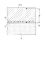
- the ceramic / aluminum bonded body includes a ceramic substrate 11 as a ceramic member made of AlN, a circuit layer 12 in which an aluminum plate 22 is bonded as an aluminum member, and a metal layer 13 in which an aluminum plate 23 is bonded.
- the power module substrate 10 is used.
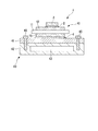
- FIG. 1 shows a power module 1 using a power module substrate 10 according to an embodiment of the present invention.
- This power module 1 includes a power module substrate 10 in which a circuit layer 12 and a metal layer 13 are disposed on a ceramic substrate 11, and a first solder layer 2 on one surface (upper surface in FIG. 1) of the circuit layer 12. And the heat sink 40 joined to the other surface (the lower surface in FIG. 1) of the metal layer 13 via the second solder layer 4.
- the first solder layer 2 and the second solder layer 4 are, for example, Sn—Ag, Sn—In, or Sn—Ag—Cu solder materials.
- Ni plating layers (not shown) are provided between the circuit layer 12 and the first solder layer 2 and between the metal layer 13 and the second solder layer 4.
- the power module substrate 10 has a ceramic substrate 11, a circuit layer 12 disposed on one surface (the upper surface in FIG. 1) of the ceramic substrate 11, and the other surface (lower surface in FIG. 1) of the ceramic substrate 11. And a disposed metal layer 13.
- the ceramic substrate 11 prevents electrical connection between the circuit layer 12 and the metal layer 13, and is composed of AlN (aluminum nitride) having high insulation in this embodiment. Further, the thickness of the ceramic substrate 11 is set within a range of 0.2 to 1.5 mm, and in this embodiment is set to 0.635 mm.
- the circuit layer 12 is formed by bonding a conductive metal plate to one surface of the ceramic substrate 11.
- the circuit layer 12 is formed by joining an aluminum plate 22 made of a rolled plate of aluminum (so-called 4N aluminum) having a purity of 99.99 mass% or more to the ceramic substrate 11. Is formed.
- a circuit pattern is formed on the circuit layer 12, and one surface (the upper surface in FIG. 1) is a mounting surface on which the semiconductor element 3 is mounted.
- the thickness of the circuit layer 12 (aluminum plate 22) is set within a range of 0.05 mm or more and less than 1.1 mm, and is set to 0.6 mm in the present embodiment.
- the metal layer 13 is formed by bonding a metal plate having excellent thermal conductivity to the other surface of the ceramic substrate 11.
- the metal layer 13 is formed by joining an aluminum plate 23 made of a rolled plate of aluminum (so-called 4N aluminum) having a purity of 99.99 mass% or more to the ceramic substrate 11. Is formed.
- the thickness of the metal layer 13 (aluminum plate 23) is set within a range of 0.05 mm or more and less than 3.0 mm, and is set to 0.6 mm in the present embodiment.
- the heat sink 40 is for cooling the power module substrate 10 described above, and includes a heat radiating plate 41 joined to the power module substrate 10 and a cooler 42 stacked on the heat radiating plate 41. ing.
- the heat radiating plate 41 spreads heat from the power module substrate 10 in the surface direction, and is a copper plate having excellent thermal conductivity in the present embodiment.
- the cooler 42 includes a flow path 43 for circulating a cooling medium (for example, cooling water).
- the cooler 42 is preferably made of a material having good thermal conductivity, and is made of A6063 (aluminum alloy) in the present embodiment.
- the heat sink 41 and the cooler 42 are fastened by a fixing screw 45 as shown in FIG.
- Mg containing oxidation which has a spinel crystal structure in the range of 2 micrometers in the thickness direction from the junction interface 30 with the ceramic substrate 11 among the circuit layer 12 and the metal layer 13.
- Object 36 is dispersed.
- the observed Mg-containing oxide 36 can be confirmed by the following method. Electron diffraction patterns were obtained for the bonding interface using a transmission electron microscope (TEM) (TII ChemSTEM manufactured by FEI, acceleration voltage 200 kV), and energy dispersive X-ray analysis (EDS) (manufactured by Thermo Scientific). The composition is analyzed using NSS7).
- TEM transmission electron microscope
- EDS energy dispersive X-ray analysis
- the electron diffraction pattern can be obtained by irradiating an electron beam focused to about 1 nm (NBD (nanobeam diffraction) method).
- This Mg-containing oxide 36 contains Mg and Al.
- the area ratio of the Mg-containing oxide 36 in the range of 2 ⁇ m in the thickness direction from the bonding interface 30 is in the range of 2% to 18%.
- a segregation portion 31 in which Mg, Si, and O segregate is formed in the vicinity of the bonding interface 30 with the ceramic substrate 11 in the circuit layer 12 and the metal layer 13.
- the segregation part 31 may be within a range of 0.01 ⁇ m in the thickness direction from the bonding interface 30 with the ceramic substrate 11 in the circuit layer 12 and the metal layer 13, but is not limited thereto.
- the ratios of Mg amount [Mg] I , Si amount [Si] I , and O amount [O] I are 1 ⁇ [Mg] S / [Mg] I ⁇ 15 and 1 ⁇ [Si] S / [Si, respectively. ] I ⁇ 25, 1 ⁇ [O] S / [O] I ⁇ 25.
- Mg amount [Mg] S , Si amount [Si] S , O amount [O] S in the segregation part 31, and Mg amount [H 10 ⁇ m away from the bonding interface 30 toward the circuit layer 12 side and the metal layer 13 side [
- the ratios of Mg] I , Si amount [Si] I , and O amount [O] I are 1.14 ⁇ [Mg] S / [Mg] I ⁇ 12.67, 1.16 ⁇ [Si] S, respectively.
- Mg amount [Mg] S in segregation part 31 is in the range of 0.1 mass% or more and 1.5 mass% or less
- Si amount [Si] S is in the range of 0.1 mass% or more and 2.5 mass% or less
- O amount [O] S is in the range of 1.5 mass% or more and 15 mass% or less.
- the amount of Cu in the segregation part 31 is 1.2 mass% or less, and the amount of Fe is 0.6 mass% or less.
- the amount of Cu in the segregation part 31 is preferably 0.00 mass% or more and 0.05 mass% or less, and the amount of Fe is preferably 0.00 mass% or more and 0.05 mass% or less, but is not limited thereto.
- the circuit layer and metal layer forming step S01 includes a stacking step S11, a heating step S12, and a molten metal solidifying step S13.
- an aluminum plate 22 is laminated on one surface of the ceramic substrate 11 via an Al—Si—Mg brazing material 24, and on the other surface of the ceramic substrate 11. Then, an aluminum plate 23 is laminated through an Al—Si—Mg-based brazing material 25 to form a laminate.
- the Al—Si—Mg-based brazing filler metals 24 and 25 include Si in a range of 1 mass% to 12 mass% and Mg in a range of 0.01 mass% to 0.05 mass%.
- the brazing material foil made of an aluminum alloy is used, and the thicknesses of the brazing materials 24 and 25 are in the range of 5 ⁇ m to 30 ⁇ m.
- heating process S12 the above-mentioned laminated body is charged in the heating furnace 29 in a state where it is pressurized in the laminating direction and heated. Then, the brazing materials 24 and 25 and a part of the aluminum plates 22 and 23 are melted to form molten metal regions at the interfaces between the aluminum plates 22 and 23 and the ceramic substrate 11.
- the conditions of this heating step S12 are: a vacuum atmosphere (10 ⁇ 4 Pa to 10 ⁇ 3 Pa) or a nitrogen atmosphere with an oxygen partial pressure of 500 volppm or less, a bonding temperature within a range of 580 ° C. to 650 ° C., heating time Is in the range of 1 minute to 180 minutes.
- the pressurizing device 50 includes a base plate 51, guide posts 52 vertically attached to the four corners of the upper surface of the base plate 51, a fixing plate 53 disposed at the upper ends of the guide posts 52, and the base plate 51. And a pressing plate 54 supported by a guide post 52 movable up and down between the fixing plate 53 and a spring provided between the fixing plate 53 and the pressing plate 54 to urge the pressing plate 54 downward. And the like, and an adjustment screw 56 for moving the fixing plate 53 up and down.
- the fixed plate 53 and the pressing plate 54 are arranged in parallel to the base plate 51, and the above-described laminate is arranged between the base plate 51 and the pressing plate 54 via the carbon sheet 57.
- the pressing device 50 has a structure in which the laminated body is pressed by moving the fixing plate 53 up and down by adjusting the position of the adjusting screw 56 and pressing the pressing plate 54 by the urging means 55. Yes.
- the thermal expansion coefficient of the guide post 52 is set to be larger than the thermal expansion coefficient of the biasing means 55. May decrease.
- the heating second process S12 using the pressure device 50, pressure load at the junction temperature described above is in the range of 0.01 kgf / cm 2 or more 1.0 kgf / cm less than 2 (less than 0.98 kPa 98 kPa) ing.
- the pressure load at the above-mentioned bonding temperature is less than 0.01 kgf / cm 2 (0.98 kPa)
- the warp of the ceramic substrate 11 may not be corrected.
- applied load at the junction temperature of the above is in a range of 0.01 kgf / cm 2 or more 1.0 kgf / cm less than 2 (less than 0.98 kPa 98 kPa).
- Pressure load at the bonding temperature of the above it is preferable to be in the range of less than 0.05 kgf / cm 2 or more 0.9 kgf / cm 2, is not limited thereto.
- the ceramic substrate 11, the aluminum plate 22, and the aluminum plate 23 are joined by solidifying the molten metal regions formed at the interfaces between the aluminum plates 22 and 23 and the ceramic substrate 11, respectively. Thereby, the power module substrate 10 in which the circuit layer 12 and the metal layer 13 are formed on the ceramic substrate 11 is manufactured.
- Heat sink joining step S02 Next, a heat radiating plate 41 is joined to the other surface (the surface opposite to the ceramic substrate 11) of the metal layer 13 of the power module substrate 10 with the second solder layer 4 interposed therebetween. Is fastened to the cooler 42 by a fixing screw 45. Thereby, the heat sink 40 and the power module substrate 10 are joined.
- semiconductor element mounting step S03 Further, the semiconductor element 3 is mounted on one surface of the circuit layer 12 (the surface opposite to the ceramic substrate 11) via the first solder layer 2. Thereby, the power module 1 which is this embodiment is produced.
- the spinel is within a range of 2 ⁇ m in the thickness direction from the bonding interface 30 with the ceramic substrate 11 of the circuit layer 12 and the metal layer 13. Since the Mg-containing oxide 36 having a crystal structure is dispersed, the oxide films formed on the surfaces of the aluminum plates 22 and 23 to be the circuit layer 12 and the metal layer 13 are sufficiently removed by reaction with Mg. The circuit layer 12 and the ceramic substrate 11 and the metal layer 13 and the ceramic substrate 11 can be reliably bonded.
- the area ratio of the Mg-containing oxide 36 within the range of 2 ⁇ m in the thickness direction from the bonding interface 30 is 2% or more, the aluminum plate to be the circuit layer 12 and the metal layer 13 The oxide films formed on the surfaces 22 and 23 can be reliably removed, and the circuit layer 12 and the ceramic substrate 11 and the metal layer 13 and the ceramic substrate 11 can be reliably bonded. Furthermore, since the area ratio of the Mg-containing oxide 36 within the range of 2 ⁇ m in the thickness direction from the bonding interface 30 is 18% or less, the Mg-containing oxide 36 does not exist excessively, and in the vicinity of the bonding interface 30. Generation of cracks and the like can be suppressed.
- Mg, Si, and O are present in the vicinity of the bonding interface 30 with the ceramic substrate 11 among the circuit layer 12 and the metal layer 13 formed by bonding the aluminum plates 22 and 23.
- the segregated portion 31 is segregated, the Mg amount [Mg] S , the Si amount [Si] S , and the O amount [O] S in the segregated portion 31, the circuit layer 12 side and the metal layer 13 side from the bonding interface 30.
- Mg amount [Mg] S , Si amount [Si] S , O amount [O] S in the segregation part 31, and H from the bonding interface 30 to the circuit layer 12 side and the metal layer 13 side.
- the ratios of Mg amount [Mg] I , Si amount [Si] I , and O amount [O] I at positions separated by 10 ⁇ m are 1 ⁇ [Mg] S / [Mg] I ⁇ 15 and 1 ⁇ , respectively.
- the ceramic substrate 11 of the circuit layer 12 and the metal layer 13 It is possible to prevent the vicinity of the bonding interface 30 from becoming excessively hard, and to prevent cracks and the like from occurring in the ceramic substrate 11.
- the pressure load at a predetermined bonding temperature is in a range of 0.01 kgf / cm 2 or more 1 kgf / cm less than 2 (less than 0.98 kPa 98 kPa)
- the interface reaction does not occur excessively, and it is possible to suppress the segregation of Mg in the vicinity of the bonding interface 30 and to segregate an appropriate amount of Mg.
- the ratios of Mg amount [Mg] I , Si amount [Si] I , and O amount [O] I are 1 ⁇ [Mg] S / [Mg] I ⁇ 15, 1 ⁇ [Si] S / [ It is possible to manufacture the power module substrate 10 in the range of Si] I ⁇ 25, 1 ⁇ [O] S / [O] I ⁇ 25.
- the power module substrate has been described as an example.
- the present invention is not limited to this, and may be a ceramic / aluminum joined body obtained by joining a ceramic member made of AlN and an aluminum member. That's fine.
- the circuit layer and the metal layer have been described as being formed by joining aluminum (4N aluminum) rolled plates having a purity of 99.99 mass% or more, but the present invention is not limited to this.
- at least one of the circuit layer and the metal layer is pure aluminum such as aluminum (2N aluminum) having a purity of 99 mass% or more or aluminum (3N aluminum) having a purity of 99.9 mass% or more, or A3003 (Si: 0.6 mass%) Fe: 0.7 mass% or less, Cu: 0.05 mass% or more and 0.20 mass% or less, Mn: 1.0 mass% or more and 1.5 mass% or less, Zn: 0.10 mass% or less, Al: balance) Any material composed of an aluminum alloy may be used.
- the circuit layer may be composed of a copper plate made of copper or a copper alloy, a laminated plate of aluminum and copper, or the like. If the circuit layer is made of an aluminum plate, the metal layer may be made of a copper plate made of copper or a copper alloy, a laminated plate of aluminum and copper, or the metal layer itself is formed. It is good also as a structure which does not.
- the heat sink is not limited to the one exemplified in this embodiment, and the structure of the heat sink is not particularly limited.
- An aluminum plate constituting a circuit layer and an aluminum plate constituting a metal layer are laminated on a ceramic substrate through a brazing material (thickness 20 ⁇ m) shown in Table 1, and brazed under the conditions shown in Table 1 for evaluation.
- a power module substrate was manufactured.
- composition in segregation layer and circuit layer The composition of the segregation layer ([Mg] S , [Si] S , [O] S , Cu, Fe) and the composition in the circuit layer ([Mg] I , [Si] I , [O] I ) are as follows. Measured with The obtained power module substrate was mechanically cut in the laminating direction, and the obtained cross section was mechanically polished to a thickness of about 50 ⁇ m to obtain a cross section sample. Thereafter, argon ions of 4 kV were incident near the bonding interface at an angle of 4 degrees from the top and bottom (surface perpendicular to the stacking direction), and thinned until sputtering was performed on the cross-sectional sample.
- the electron diffraction pattern was obtained by irradiating an electron beam focused to about 1 nm (NBD method).
- N and Mg were mapped in a range of 2 ⁇ m in the thickness direction from the bonding interface between the ceramic substrate and the metal layer using a transmission electron microscope (Titan ChemiSTEM manufactured by FEI) at a magnification of 10,000 times.
- the boundary between the region where N is detected and the region where it is not detected is defined as the bonding interface, and the region of Mg concentration of 6 to 12 at% is determined as Mg-containing oxide based on the mapping of Mg.
- the area ratio of the Mg-containing oxide was determined. The measurement was performed at five locations, and the average value was defined as the area ratio.
- Table 3 shows the area ratio in the range of 2 ⁇ m from the bonding interface of the Mg-containing oxide having a spinel crystal structure in the thickness direction.
- a heat sink was joined to the other surface side of the metal layer of the power module substrate described above.
- the heat sink was an aluminum plate of A3003 alloy measuring 50 mm x 60 mm x 5 mm.
- the joining conditions were joining by heating at 610 ° C. in a vacuum with Al-Si brazing foil being pressurized at 3.0 kgf / cm 2 (0.29 MPa).
- a heat cycle test was carried out using the power module substrate with a heat sink thus obtained.
- the thermal shock tester uses TSPE-51 manufactured by Espec Co., Ltd., one cycle of liquid phase (Fluorinert) for 5 minutes at -40 ° C and 5 minutes at 150 ° C with respect to the power module substrate with heat sink. And 2000 cycles were carried out. Thereafter, the bonding rate between the circuit layer and the ceramic substrate was evaluated as follows. In addition, evaluation of the joining rate was performed before the thermal cycle test (initial joining rate) and after the thermal cycling test (post-cycle joining rate).
- the bonding rate was performed using an ultrasonic flaw detector (FineSAT 200, manufactured by Hitachi Power Solutions Co., Ltd.) for the bonding rate at the interface between the ceramic substrate and the metal layer with respect to the power module substrate with a heat sink.
- the joining rate was calculated.
- the evaluation results are shown in Table 3.
- the initial bonding area is the area to be bonded before bonding, that is, the area of the metal layer (37 mm ⁇ 37 mm) in this embodiment.
- the peeling is indicated by the white portion in the joint portion. Therefore, the area of the white portion is defined as the peeling area.
- (Bonding rate) ⁇ (initial bonding area) ⁇ (peeling area) ⁇ / (initial bonding area) ⁇ 100
- the ceramic member and the aluminum member are reliably joined, and it is excellent in the joining reliability at the time of a thermal cycle load, and can suppress generation
- a power module including the substrate and the power module substrate.
- Ceramic substrate ceramic / aluminum bonded body
- Ceramic substrate ceramic member
- Circuit layer aluminum member
- Metal layer aluminum member
- Al—Si—Mg brazing filler metal Al—Si—Mg brazing filler metal
Abstract
Description
本願は、2015年11月6日に、日本に出願された特願2015-218892号に基づき優先権を主張し、その内容をここに援用する。 The present invention includes a ceramic / aluminum bonded body formed by bonding a ceramic member made of AlN and an aluminum member, a power module substrate including a ceramic substrate formed of AlN and an aluminum plate bonded to the ceramic substrate, and The present invention relates to a power module including the power module substrate.
This application claims priority on November 6, 2015 based on Japanese Patent Application No. 2015-218892 for which it applied to Japan, and uses the content here.
風力発電、電気自動車、ハイブリッド自動車等を制御するために用いられる大電力制御用のパワー半導体素子においては、発熱量が多い。そのため、パワー半導体素子を搭載する基板としては、例えばAlN(窒化アルミ-ニウム)、Al2O3(アルミナ)などからなるセラミックス基板と、このセラミックス基板の一方の面に導電性の優れた金属板を接合して形成した回路層と、を備えたパワーモジュール用基板が、従来から広く用いられている。なお、パワージュール用基板としては、セラミックス基板の他方の面に金属板を接合して金属層が形成したものも提供されている。 Semiconductor devices such as LEDs and power modules have a structure in which a semiconductor element is bonded on a circuit layer made of a conductive material.
Power semiconductor elements for high power control used for controlling wind power generation, electric vehicles, hybrid vehicles, and the like generate a large amount of heat. Therefore, as a substrate on which the power semiconductor element is mounted, for example, a ceramic substrate made of AlN (aluminum nitride), Al 2 O 3 (alumina) or the like, and a metal plate having excellent conductivity on one surface of the
このようなパワーモジュール用基板においては、回路層の上に、はんだ層を介してパワー素子としての半導体素子が搭載され、パワーモジュールとして使用される。また、金属層側には、はんだを介して銅製のヒートシンクが接合されることもある。 For example, in
In such a power module substrate, a semiconductor element as a power element is mounted on a circuit layer via a solder layer and used as a power module. Moreover, a copper heat sink may be joined to the metal layer side via solder.
これらのセラミックス回路基板においては、偏在させたMgによって接合を阻害する酸化物を除去することにより、セラミックス基板とアルミニウム板との接合性の向上を図っている。 In Patent Documents 2-5, a ceramic substrate and an aluminum plate are bonded using a brazing material containing Mg, and Mg or the like is bonded to the bonding interface between the brazing material and the aluminum plate or between the brazing material and the ceramic substrate. There has been proposed a ceramic circuit board with uneven distribution.
In these ceramic circuit boards, the oxide that obstructs bonding by the unevenly distributed Mg is removed, thereby improving the bondability between the ceramic board and the aluminum plate.
さらに、接合界面から前記アルミニウム部材側に10μm離間した位置におけるMg量[Mg]Iが0.8mass%以下とされているので、アルミニウム部材自体が硬くなることを抑制でき、アルミニウム部材の変形抵抗が上昇してしまうことを抑制できる。 Further, the ceramic / aluminum bonded body described above has a segregated portion where Mg, Si, and O are segregated, and Mg amount [Mg] S , Si amount [Si] S , and O amount [O] S in the segregated portion. And the ratio of Mg amount [Mg] I , Si amount [Si] I , O amount [O] I at a
Furthermore, since the Mg amount [Mg] I at a
この場合、前記偏析部において、Cu量が1.2mass%以下、Fe量が0.6mass%以下に制限されているので、アルミニウム部材のうちセラミックス部材との接合界面近傍が、過剰に硬くなることを抑制でき、セラミックス部材に亀裂等が生じることを抑制できる。 Here, in the ceramic / aluminum bonded body according to one aspect of the present invention, it is preferable that the segregation portion has a Cu content of 1.2 mass% or less and an Fe content of 0.6 mass% or less.
In this case, since the amount of Cu is limited to 1.2 mass% or less and the amount of Fe is limited to 0.6 mass% or less in the segregated portion, the vicinity of the bonding interface with the ceramic member of the aluminum member becomes excessively hard. It can suppress that a crack etc. arise in a ceramic member.
さらに、接合界面から前記アルミニウム板側に10μm離間した位置におけるMg量[Mg]Iが0.8mass%以下とされているので、アルミニウム板の変形抵抗が高くなることを抑制できる。 In the power module substrate described above, Mg, Si, and O are segregated in the vicinity of the bonding interface between the aluminum plate and the ceramic substrate, so that the interface energy is stabilized and the bonding reliability between the aluminum plate and the ceramic substrate is improved. Can be improved. Moreover, it can suppress that the joining interface vicinity with a ceramic substrate among aluminum plates becomes hard too much, and when a thermal cycle is loaded to this power module substrate, it can suppress that a crack etc. arise in a ceramic substrate.
Furthermore, since the Mg amount [Mg] I at a
この場合、前記偏析部において、Cu量が1.2mass%以下、Fe量が0.6mass%以下に制限されているので、アルミニウム板のうちセラミックス基板との接合界面近傍が、過剰に硬くなることを抑制でき、このパワーモジュール用基板に冷熱サイクルを負荷した際に、セラミックス基板に亀裂等が生じることを抑制できる。 Here, in the power module substrate according to an aspect of the present invention, it is preferable that the segregation portion has a Cu amount of 1.2 mass% or less and an Fe amount of 0.6 mass% or less.
In this case, since the amount of Cu is limited to 1.2 mass% or less and the amount of Fe is limited to 0.6 mass% or less in the segregated portion, the vicinity of the bonding interface with the ceramic substrate in the aluminum plate becomes excessively hard. It is possible to suppress the occurrence of cracks and the like in the ceramic substrate when a cooling cycle is loaded on the power module substrate.
この構成のパワーモジュールにおいては、上述のパワーモジュール用基板を備えているので、セラミックス基板とアルミニウム板とが強固に接合されており、信頼性に特に優れている。 A power module according to one embodiment of the present invention includes the above-described power module substrate and a semiconductor element.
Since the power module having this configuration includes the above-described power module substrate, the ceramic substrate and the aluminum plate are firmly bonded, and the reliability is particularly excellent.
このパワーモジュール1は、回路層12及び金属層13がセラミックス基板11に配設されたパワーモジュール用基板10と、回路層12の一方の面(図1において上面)に第1はんだ層2を介して接合された半導体素子3と、金属層13の他方の面(図1において下面)に第2はんだ層4を介して接合されたヒートシンク40と、を備えている。
ここで、第1はんだ層2及び第2はんだ層4は、例えばSn-Ag系、Sn-In系、若しくはSn-Ag-Cu系のはんだ材とされている。なお、本実施形態では、回路層12と第1はんだ層2との間、及び、金属層13と第2はんだ層4との間にNiめっき層(図示なし)が設けられている。 FIG. 1 shows a
This
Here, the
セラミックス基板11は、回路層12と金属層13との間の電気的接続を防止するものであって、本実施形態では、絶縁性の高いAlN(窒化アルミニウム)で構成されている。また、セラミックス基板11の厚さは、0.2~1.5mmの範囲内に設定されており、本実施形態では、0.635mmに設定されている。 The
The
放熱板41は、前述のパワーモジュール用基板10からの熱を面方向に拡げるものであり、本実施形態では、熱伝導性に優れた銅板とされている。
冷却器42は、図1に示すように、冷却媒体(例えば冷却水)を流通するための流路43を備えている。冷却器42は、熱伝導性が良好な材質で構成されることが望ましく、本実施形態においては、A6063(アルミニウム合金)で構成されている。
なお、放熱板41と冷却器42とは、図1に示すように、固定ネジ45によって締結されている。 The
The
As shown in FIG. 1, the cooler 42 includes a
In addition, the
なお、観察されたMg含有酸化物36は、以下の方法により確認できる。
接合界面に対し、透過型電子顕微鏡(TEM)(FEI社製Titan ChemiSTEM、加速電圧200kV)を用いて電子回折図形を得て、エネルギー分散型X線分析法(EDS)(サーモサイエンティフィック社製NSS7)を用いて組成を分析する。電子回折図形からスピネル構造と同定された領域かつ組成がMg=6~12at%,O=30~60at%,Al=残部となっている領域をMg含有酸化物36とする。なお、電子回折図形は、1nm程度に絞った電子ビームを照射することで得る(NBD(ナノビーム回折)法)。 And in this embodiment, as shown in FIG. 2, Mg containing oxidation which has a spinel crystal structure in the range of 2 micrometers in the thickness direction from the
The observed Mg-containing
Electron diffraction patterns were obtained for the bonding interface using a transmission electron microscope (TEM) (TII ChemSTEM manufactured by FEI, acceleration voltage 200 kV), and energy dispersive X-ray analysis (EDS) (manufactured by Thermo Scientific). The composition is analyzed using NSS7). The region identified as the spinel structure from the electron diffraction pattern and the region where the composition is Mg = 6 to 12 at%, O = 30 to 60 at%, and Al = the balance is defined as the Mg-containing
ここで、偏析部31におけるMg量[Mg]S,Si量[Si]S,O量[O]Sと、接合界面30から回路層12側及び金属層13側にH=10μm離間した位置におけるMg量[Mg]I,Si量[Si]I,O量[O]Iとの比が、それぞれ、1<[Mg]S/[Mg]I≦15,1<[Si]S/[Si]I≦25,1<[O]S/[O]I≦25の範囲内とされている。偏析部31におけるMg量[Mg]S,Si量[Si]S,O量[O]Sと、接合界面30から回路層12側及び金属層13側にH=10μm離間した位置におけるMg量[Mg]I,Si量[Si]I,O量[O]Iとの比は、それぞれ、1.14<[Mg]S/[Mg]I≦12.67,1.16<[Si]S/[Si]I≦12.67,1.45<[O]S/[O]I≦11.73であることが好ましく、1.52<[Mg]S/[Mg]I≦5.50,2.31<[Si]S/[Si]I≦8.35,1.93<[O]S/[O]I≦7.64であることがより好ましいが、これに限定されることはない。
なお、偏析部31におけるMg量[Mg]Sが0.1mass%以上1.5mass%以下の範囲内、Si量[Si]Sが0.1mass%以上2.5mass%以下の範囲内、O量[O]Sが1.5mass%以上15mass%以下の範囲内とされている。 In the present embodiment, as shown in FIG. 2, a
Here, the amount of Mg [Mg] S , the amount of Si [Si] S , and the amount of O [O] S in the
In addition, Mg amount [Mg] S in
さらに、本実施形態においては、偏析部31におけるCu量が1.2mass%以下、Fe量が0.6mass%以下とされている。偏析部31におけるCu量は0.00mass%以上、0.05mass%以下、Fe量は0.00mass%以上、0.05mass%以下であることが好ましいが、これに限定されることはない。 In this embodiment, the Mg amount [Mg] I at a position where H = 10 μm away from the
Furthermore, in this embodiment, the amount of Cu in the
まず、アルミニウム板22,23とセラミックス基板11とを接合し、回路層12及び金属層13を形成する。
本実施形態では、図3に示すように、回路層及び金属層形成工程S01は、積層工程S11と加熱工程S12と溶融金属凝固工程S13と、を備えている。 (Circuit layer and metal layer forming step S01)
First, the
In the present embodiment, as shown in FIG. 3, the circuit layer and metal layer forming step S01 includes a stacking step S11, a heating step S12, and a molten metal solidifying step S13.
そして、加圧装置50は、調整ネジ56の位置を調節することによって固定板53を上下させて、付勢手段55により押圧板54を押し込むことで、積層体が加圧される構造を備えている。
この加圧装置50においては、ガイドポスト52の熱膨張係数が、付勢手段55の熱膨張係数よりも大きく設定されており、室温で加圧した状態で接合温度まで加熱すると、加圧荷重が低下するおそれがある。 The fixed
The
In this
ここで、上述の接合温度における加圧荷重が0.01kgf/cm2(0.98kPa)未満の場合には、セラミックス基板11の反りを矯正することができないおそれがある。また、溶融金属領域が形成された時点でアルミニウム板22,23の位置ズレが生じるおそれがある。一方、上述の接合温度における加圧荷重が1.0kgf/cm2(98kPa)以上の場合には、接合界面におけるMgの偏析量が多くなり過ぎて、接合信頼性が低下してしまうおそれがある。
以上のことから、本実施形態においては、上述の接合温度における加圧荷重が0.01kgf/cm2以上1.0kgf/cm2未満(0.98kPa以上98kPa未満)の範囲内とされている。上述の接合温度における加圧荷重は0.05kgf/cm2以上0.9kgf/cm2未満の範囲内とされることが好ましいが、これに限定されることはない。 Therefore, the heating second process S12 using the
Here, when the pressure load at the above-mentioned bonding temperature is less than 0.01 kgf / cm 2 (0.98 kPa), the warp of the
From the above, in this embodiment, applied load at the junction temperature of the above is in a range of 0.01 kgf / cm 2 or more 1.0 kgf / cm less than 2 (less than 0.98 kPa 98 kPa). Pressure load at the bonding temperature of the above it is preferable to be in the range of less than 0.05 kgf / cm 2 or more 0.9 kgf / cm 2, is not limited thereto.
これにより、セラミックス基板11に回路層12及び金属層13が形成されたパワーモジュール用基板10が製造される。 In the molten metal solidification step S <b> 13, the
Thereby, the
次に、このパワーモジュール用基板10の金属層13の他方の面(セラミックス基板11とは反対側の面)に、第2はんだ層4を介して放熱板41を接合するとともに、この放熱板41を固定ネジ45によって冷却器42に締結する。これにより、ヒートシンク40とパワーモジュール用基板10とが接合される。 (Heat sink joining step S02)
Next, a
また、回路層12の一方の面(セラミックス基板11とは反対側の面)に第1はんだ層2を介して半導体素子3を搭載する。これにより、本実施形態であるパワーモジュール1が製出される。 (Semiconductor element mounting step S03)
Further, the
さらに、接合界面30から厚さ方向に2μmの範囲内におけるMg含有酸化物36の面積率が18%以下とされているので、Mg含有酸化物36が過剰に存在せず、接合界面30近傍におけるクラックの発生等を抑制することができる。 Here, in this embodiment, since the area ratio of the Mg-containing
Furthermore, since the area ratio of the Mg-containing
また、回路層12及び金属層13のうちセラミックス基板11との接合界面30近傍が、過剰に硬くなることを抑制でき、このパワーモジュール用基板10に冷熱サイクルを負荷した際に、セラミックス基板11に亀裂等が生じることを抑制できる。 In the
Moreover, it can suppress that the joining
このため、本実施形態においては、偏析部31におけるMg量[Mg]S,Si量[Si]S,O量[O]Sと、接合界面30から回路層12側及び金属層13側にH=10μm離間した位置におけるMg量[Mg]I,Si量[Si]I,O量[O]I、との比を、それぞれ、1<[Mg]S/[Mg]I≦15,1<[Si]S/[Si]I≦25,1<[O]S/[O]I≦25の範囲内に設定している。 Here, when [Mg] S / [Mg] I is 1 or less, [Si] S / [Si] I is 1 or less, and [O] S / [O] I is 1 or less, the
For this reason, in the present embodiment, Mg amount [Mg] S , Si amount [Si] S , O amount [O] S in the
特に、本実施形態においては、偏析部31において、Cu量が1.2mass%以下、Fe量が0.6mass%以下に制限されているので、回路層12及び金属層13のうちセラミックス基板11との接合界面30近傍が、過剰に硬くなることを抑制でき、セラミックス基板11に亀裂等が生じることを抑制できる。 Furthermore, since the Mg amount [Mg] I at a position separated by H = 10 μm from the
In particular, in the present embodiment, in the
例えば、本実施形態では、パワーモジュール用基板を例に挙げて説明したが、これに限定されることはなく、AlNからなるセラミックス部材とアルミニウム部材とを接合してなるセラミックス/アルミニウム接合体であればよい。 As mentioned above, although embodiment of this invention was described, this invention is not limited to this, It can change suitably in the range which does not deviate from the technical idea of the invention.
For example, in the present embodiment, the power module substrate has been described as an example. However, the present invention is not limited to this, and may be a ceramic / aluminum joined body obtained by joining a ceramic member made of AlN and an aluminum member. That's fine.
さらに、金属層がアルミニウム板で構成されている場合であれば、回路層を、銅又は銅合金からなる銅板、アルミニウムと銅との積層板等で構成してもよい。また、回路層がアルミニウム板で構成されている場合であれば、金属層を、銅又は銅合金からなる銅板、アルミニウムと銅との積層板等で構成してもよいし、金属層自体を形成しない構造としてもよい。 In the present embodiment, the circuit layer and the metal layer have been described as being formed by joining aluminum (4N aluminum) rolled plates having a purity of 99.99 mass% or more, but the present invention is not limited to this. And at least one of the circuit layer and the metal layer is pure aluminum such as aluminum (2N aluminum) having a purity of 99 mass% or more or aluminum (3N aluminum) having a purity of 99.9 mass% or more, or A3003 (Si: 0.6 mass%) Fe: 0.7 mass% or less, Cu: 0.05 mass% or more and 0.20 mass% or less, Mn: 1.0 mass% or more and 1.5 mass% or less, Zn: 0.10 mass% or less, Al: balance) Any material composed of an aluminum alloy may be used.
Furthermore, if the metal layer is composed of an aluminum plate, the circuit layer may be composed of a copper plate made of copper or a copper alloy, a laminated plate of aluminum and copper, or the like. If the circuit layer is made of an aluminum plate, the metal layer may be made of a copper plate made of copper or a copper alloy, a laminated plate of aluminum and copper, or the metal layer itself is formed. It is good also as a structure which does not.
また、ヒートシンクは、本実施形態で例示してものに限定されることはなく、ヒートシンクの構造に特に限定はない。 Furthermore, although it demonstrated as what forms a Ni plating layer in the surface which performs a solder joint of a circuit layer and a metal layer, it is not limited to this, Even if it comprises an underlayer by other means, such as Ag paste Good.
Further, the heat sink is not limited to the one exemplified in this embodiment, and the structure of the heat sink is not particularly limited.
回路層を構成するアルミニウム板として、表1に示す組成及び厚さの圧延板(37mm×37mm)を準備した。
また、セラミックス基板として、表1に示す組成及び厚さのもの(40mm×40mm)を準備した。
さらに、金属層を構成するアルミニウム板として、純度99.99mass%以上のアルミニウム(4Nアルミニウム)の圧延板(37mm×37mm×厚さ1.6mm)を準備した。 A confirmation experiment conducted to confirm the effectiveness of the present invention will be described.
As an aluminum plate constituting the circuit layer, a rolled plate (37 mm × 37 mm) having the composition and thickness shown in Table 1 was prepared.
Moreover, the thing (40 mm x 40 mm) of the composition and thickness shown in Table 1 was prepared as a ceramic substrate.
Furthermore, as an aluminum plate constituting the metal layer, an aluminum (4N aluminum) rolled plate (37 mm × 37 mm × thickness 1.6 mm) having a purity of 99.99 mass% or more was prepared.
偏析層の組成([Mg]S,[Si]S,[O]S,Cu,Fe)及び回路層内の組成([Mg]I,[Si]I,[O]I)は次の方法で測定した。
得られたパワーモジュール用基板を積層方向に機械切断し、得られた断面を厚さ約50μmまで機械研磨し、断面試料とした。その後、接合界面付近に4kVのアルゴンイオンを上下(積層方向と垂直の面)から4度の角度で入射させ、スパッタリングで断面試料に穴が開くまで薄片化した。穴の縁がエッジ状になって電子線が透過可能な厚さ0.1μm程度となるので、この部分をTEM及びEDSで測定し、偏析層の組成を測定した。
TEM及びEDSの測定は、FEI社製Titan ChemiSTEM(EDS検出器付)、加速電圧:200kV、ビーム径:1nm、倍率:100万倍で行った。
また、接合界面から10μmアルミニウム板側に離間した位置における組成を回路層内の組成とした。
測定は5箇所行い、その平均値を組成とした。 評価結果を表2に示す。 (Composition in segregation layer and circuit layer)
The composition of the segregation layer ([Mg] S , [Si] S , [O] S , Cu, Fe) and the composition in the circuit layer ([Mg] I , [Si] I , [O] I ) are as follows. Measured with
The obtained power module substrate was mechanically cut in the laminating direction, and the obtained cross section was mechanically polished to a thickness of about 50 μm to obtain a cross section sample. Thereafter, argon ions of 4 kV were incident near the bonding interface at an angle of 4 degrees from the top and bottom (surface perpendicular to the stacking direction), and thinned until sputtering was performed on the cross-sectional sample. Since the edge of the hole becomes an edge and becomes a thickness of about 0.1 μm through which the electron beam can be transmitted, this portion was measured by TEM and EDS, and the composition of the segregation layer was measured.
The measurement of TEM and EDS was performed at Titan ChemiSTEM (with EDS detector) manufactured by FEI, acceleration voltage: 200 kV, beam diameter: 1 nm, and magnification: 1 million times.
Further, the composition in the position separated from the bonding interface to the 10 μm aluminum plate side was defined as the composition in the circuit layer.
The measurement was performed at five locations, and the average value was taken as the composition. The evaluation results are shown in Table 2.
セラミックス基板と金属層との接合界面から厚さ方向に2μmの範囲内に対し、透過型電子顕微鏡(FEI社製Titan ChemiSTEM、加速電圧200kV)を用いて電子回折図形を得て、エネルギー分散型X線分析法(サーモサイエンティフィック社製NSS7)を用いて組成を分析した。その後、電子回折図形からスピネル構造と同定された領域かつ組成がMg=6~12at%,O=30~60at%,Al=残部となっている領域をMg含有酸化物とし、Mg含有酸化物の有無を調べた。なお、電子回折図形は、1nm程度に絞った電子ビームを照射することで得た(NBD法)。
次に、セラミックス基板と金属層との接合界面から厚さ方向に2μmの範囲内を、透過型電子顕微鏡(FEI社製Titan ChemiSTEM)を用い、倍率10000倍でN及びMgのマッピングを行った。Nの検出される領域とされない領域の境界を接合界面とし、MgのマッピングからMg濃度6~12at%の領域をMg含有酸化物とし、2値化後に、Mg含有酸化物の面積を測定面積で割ることにより、Mg含有酸化物の面積率を求めた。測定は5ヶ所行い、その平均値を面積率とした。
スピネル結晶構造を有するMg含有酸化物の接合界面から厚さ方向に2μmの範囲内における面積率を表3に示す。 (Measurement of area ratio of Mg-containing oxide having spinel crystal structure)
An energy dispersive X is obtained with a transmission electron microscope (Titan ChemiSTEM manufactured by FEI Co., Ltd., acceleration voltage 200 kV) within a range of 2 μm in the thickness direction from the bonding interface between the ceramic substrate and the metal layer. The composition was analyzed using line analysis (Thermo Scientific NSS7). Thereafter, the region identified as the spinel structure from the electron diffraction pattern and the region where the composition is Mg = 6 to 12 at%, O = 30 to 60 at%, and Al = the balance is defined as the Mg-containing oxide. The presence or absence was examined. The electron diffraction pattern was obtained by irradiating an electron beam focused to about 1 nm (NBD method).
Next, N and Mg were mapped in a range of 2 μm in the thickness direction from the bonding interface between the ceramic substrate and the metal layer using a transmission electron microscope (Titan ChemiSTEM manufactured by FEI) at a magnification of 10,000 times. The boundary between the region where N is detected and the region where it is not detected is defined as the bonding interface, and the region of Mg concentration of 6 to 12 at% is determined as Mg-containing oxide based on the mapping of Mg. By dividing, the area ratio of the Mg-containing oxide was determined. The measurement was performed at five locations, and the average value was defined as the area ratio.
Table 3 shows the area ratio in the range of 2 μm from the bonding interface of the Mg-containing oxide having a spinel crystal structure in the thickness direction.
上述のパワーモジュール用基板の金属層の他方の面側にヒートシンクを接合した。ヒートシンクは、50mm×60mm×5mmtのA3003合金のアルミニウム板とした。
接合条件は、Al-Siろう箔を用いて、3.0kgf/cm2(0.29MPa)で加圧した状態で、真空中にて、610℃で加熱することによる接合とした。
このようにして得られたヒートシンク付パワーモジュール用基板を用いて、冷熱サイクル試験を実施した。 (Joining rate)
A heat sink was joined to the other surface side of the metal layer of the power module substrate described above. The heat sink was an aluminum plate of A3003 alloy measuring 50 mm x 60 mm x 5 mm.
The joining conditions were joining by heating at 610 ° C. in a vacuum with Al-Si brazing foil being pressurized at 3.0 kgf / cm 2 (0.29 MPa).
A heat cycle test was carried out using the power module substrate with a heat sink thus obtained.
ここで、初期接合面積とは、接合前における接合すべき面積、すなわち本実施例では金属層の面積(37mm×37mm)とした。超音波探傷像を二値化処理した画像において剥離は接合部内の白色部で示されることから、この白色部の面積を剥離面積とした。
(接合率)={(初期接合面積)-(剥離面積)}/(初期接合面積)×100 Evaluation of the bonding rate was performed using an ultrasonic flaw detector (FineSAT 200, manufactured by Hitachi Power Solutions Co., Ltd.) for the bonding rate at the interface between the ceramic substrate and the metal layer with respect to the power module substrate with a heat sink. The joining rate was calculated. The evaluation results are shown in Table 3.
Here, the initial bonding area is the area to be bonded before bonding, that is, the area of the metal layer (37 mm × 37 mm) in this embodiment. In the image obtained by binarizing the ultrasonic flaw detection image, the peeling is indicated by the white portion in the joint portion. Therefore, the area of the white portion is defined as the peeling area.
(Bonding rate) = {(initial bonding area) − (peeling area)} / (initial bonding area) × 100
上述のヒートシンク付パワーモジュール用基板を用いて、冷熱サイクル試験を実施した。測定条件を以下に示す。2000サイクル後に、セラミックス基板の割れの有無を、超音波探傷装置を用いて確認した。評価結果を表3に示す。
評価装置:エスペック株式会社製TSB-51
液相:フロリナート
温度条件:-40℃で5分と150℃で5分を1サイクルとする。 (Ceramic substrate cracks)
A thermal cycle test was performed using the above-mentioned power module substrate with a heat sink. The measurement conditions are shown below. After 2000 cycles, the presence or absence of cracks in the ceramic substrate was confirmed using an ultrasonic flaw detector. The evaluation results are shown in Table 3.
Evaluation device: TSB-51 manufactured by ESPEC Corporation
Liquid phase: Fluorinert Temperature conditions: One cycle of -40 ° C for 5 minutes and 150 ° C for 5 minutes.


一方、Mg,Si,Oの比が本発明の範囲内より小さい比較例1,4,6では接合率の低下が確認された。Mg,Si,Oの比が本発明の範囲内より大きい比較例2,5,7や、[Mg]Iが0.8mass%を超えた比較例3では、セラミックス基板の割れが確認された。また、セラミックス基板にAl2O3を用いた比較例8では、[Mg]S/[Mg]Iが本発明の範囲外となり、冷熱サイクル試験後の接合率が低下した。 In Invention Examples 1 to 18 in which the ratio of Mg, Si, and O in the segregated portion is within the range of the present invention, the initial bonding rate is high, and the ceramic substrate is not cracked after the thermal cycle test, and the bonding reliability It was also confirmed that it was high.
On the other hand, in Comparative Examples 1, 4, and 6 in which the ratio of Mg, Si, and O is smaller than the range of the present invention, a decrease in the bonding rate was confirmed. In Comparative Examples 2, 5, and 7 in which the ratio of Mg, Si, and O was larger than within the scope of the present invention and in Comparative Example 3 in which [Mg] I exceeded 0.8 mass%, cracks in the ceramic substrate were confirmed. In Comparative Example 8 using Al 2 O 3 to the ceramic substrate, [Mg] S / [Mg ] I is beyond the scope of the present invention, the junction rate after thermal cycle test was reduced.
11 セラミックス基板(セラミックス部材)
12 回路層(アルミニウム部材)
13 金属層(アルミニウム部材)
24 Al-Si-Mg系ろう材
25 Al-Si-Mg系ろう材 10 Power module substrate (ceramic / aluminum bonded body)
11 Ceramic substrate (ceramic member)
12 Circuit layer (aluminum member)
13 Metal layer (aluminum member)
24 Al—Si—Mg brazing
Claims (5)
- AlNからなるセラミックス部材と、アルミニウム部材とが接合されてなるセラミックス/アルミニウム接合体であって、
前記アルミニウム部材のうち前記セラミックス部材との接合界面から厚さ方向に2μmの範囲内に、スピネル結晶構造を有するMg含有酸化物が分散しており、
前記アルミニウム部材のうち前記セラミックス部材との接合界面近傍領域に、Mg,Si,Oが偏析した偏析部を有し、
前記偏析部におけるMg量[Mg]S,Si量[Si]S,O量[O]Sと、接合界面から前記アルミニウム部材側に10μm離間した位置におけるMg量[Mg]I,Si量[Si]I,O量[O]I、との比が、それぞれ、
1<[Mg]S/[Mg]I≦15,
1<[Si]S/[Si]I≦25,
1<[O]S/[O]I≦25
の範囲内とされるとともに、接合界面から前記アルミニウム部材側に10μm離間した位置におけるMg量[Mg]Iが0.8mass%以下とされているセラミックス/アルミニウム接合体。 A ceramic / aluminum joined body in which a ceramic member made of AlN and an aluminum member are joined,
The Mg-containing oxide having a spinel crystal structure is dispersed within a range of 2 μm in the thickness direction from the bonding interface with the ceramic member among the aluminum members,
In the aluminum member, in the vicinity of the bonding interface with the ceramic member, there is a segregated portion in which Mg, Si, O segregates,
The polarized Mg amount in the analyzing unit [Mg] S, Si content [Si] S, O amount [O] S and, Mg amount in 10μm spaced locations in the aluminum member side from the bonding interface [Mg] I, Si amount [Si ] The ratio of I and O amount [O] I is
1 <[Mg] S / [Mg] I ≦ 15,
1 <[Si] S / [Si] I ≦ 25,
1 <[O] S / [O] I ≦ 25
And an Mg amount [Mg] I at a position 10 μm apart from the bonding interface toward the aluminum member side is 0.8 mass% or less. - 前記偏析部において、Cu量が1.2mass%以下、Fe量が0.6mass%以下とされている請求項1に記載のセラミックス/アルミニウム接合体。 2. The ceramic / aluminum bonded body according to claim 1, wherein in the segregated portion, the Cu content is 1.2 mass% or less and the Fe content is 0.6 mass% or less.
- AlNからなるセラミックス基板と、このセラミックス基板に接合されたアルミニウム板とを備えたパワーモジュール用基板であって、
前記アルミニウム板のうち前記セラミックス基板との接合界面から厚さ方向に2μmの範囲内に、スピネル結晶構造を有するMg含有酸化物が分散しており、
前記アルミニウム板のうち前記セラミックス基板との接合界面近傍領域に、Mg,Si,Oが偏析した偏析部を有し、
前記偏析部におけるMg量[Mg]S,Si量[Si]S,O量[O]Sと、接合界面から前記アルミニウム板側に10μm離間した位置におけるMg量[Mg]I,Si量[Si]I,O量[O]I、との比が、それぞれ、
1<[Mg]S/[Mg]I≦15,
1<[Si]S/[Si]I≦25,
1<[O]S/[O]I≦25
の範囲内とされるとともに、接合界面から前記アルミニウム板側に10μm離間した位置におけるMg量[Mg]Iが0.8mass%以下とされているパワーモジュール用基板。 A power module substrate comprising a ceramic substrate made of AlN and an aluminum plate bonded to the ceramic substrate,
An Mg-containing oxide having a spinel crystal structure is dispersed within a range of 2 μm in the thickness direction from the bonding interface with the ceramic substrate in the aluminum plate,
In the aluminum plate, in the vicinity of the bonding interface with the ceramic substrate, there is a segregated portion in which Mg, Si, O segregates,
The polarized Mg amount in the analyzing unit [Mg] S, Si content [Si] S, O amount [O] S and, Mg amount in 10μm spaced locations on the aluminum plate side from the bonding interface [Mg] I, Si amount [Si ] The ratio of I and O amount [O] I is
1 <[Mg] S / [Mg] I ≦ 15,
1 <[Si] S / [Si] I ≦ 25,
1 <[O] S / [O] I ≦ 25
And the Mg amount [Mg] I at a position spaced 10 μm away from the bonding interface toward the aluminum plate is 0.8 mass% or less. - 前記偏析部において、Cu量が1.2mass%以下、Fe量が0.6mass%以下とされている請求項3に記載のパワーモジュール用基板。 4. The power module substrate according to claim 3, wherein, in the segregation part, the Cu amount is 1.2 mass% or less and the Fe amount is 0.6 mass% or less.
- 請求項3又は請求項4に記載のパワーモジュール用基板と、半導体素子と、を備えるパワーモジュール。 A power module comprising the power module substrate according to claim 3 or 4 and a semiconductor element.
Priority Applications (4)
| Application Number | Priority Date | Filing Date | Title |
|---|---|---|---|
| KR1020187012059A KR102462273B1 (en) | 2015-11-06 | 2016-08-29 | Ceramics/aluminum assembly, substrate for power module, and power module |
| EP16861830.4A EP3372573B1 (en) | 2015-11-06 | 2016-08-29 | Ceramic-aluminum conjugate, power module substrate, and power module |
| CN201680063775.0A CN108137420B (en) | 2015-11-06 | 2016-08-29 | Ceramic/aluminum bonded body, substrate for power module, and power module |
| US15/771,595 US10607907B2 (en) | 2015-11-06 | 2016-08-29 | Ceramic-aluminum conjugate, power module substrate, and power module |
Applications Claiming Priority (2)
| Application Number | Priority Date | Filing Date | Title |
|---|---|---|---|
| JP2015218892A JP6656657B2 (en) | 2015-11-06 | 2015-11-06 | Ceramic / aluminum joint, power module substrate, and power module |
| JP2015-218892 | 2015-11-06 |
Publications (1)
| Publication Number | Publication Date |
|---|---|
| WO2017077761A1 true WO2017077761A1 (en) | 2017-05-11 |
Family
ID=58661874
Family Applications (1)
| Application Number | Title | Priority Date | Filing Date |
|---|---|---|---|
| PCT/JP2016/075163 WO2017077761A1 (en) | 2015-11-06 | 2016-08-29 | Ceramic-aluminum conjugate, power module substrate, and power module |
Country Status (7)
| Country | Link |
|---|---|
| US (1) | US10607907B2 (en) |
| EP (1) | EP3372573B1 (en) |
| JP (1) | JP6656657B2 (en) |
| KR (1) | KR102462273B1 (en) |
| CN (1) | CN108137420B (en) |
| TW (1) | TWI700263B (en) |
| WO (1) | WO2017077761A1 (en) |
Cited By (1)
| Publication number | Priority date | Publication date | Assignee | Title |
|---|---|---|---|---|
| WO2020044590A1 (en) * | 2018-08-28 | 2020-03-05 | 三菱マテリアル株式会社 | Copper/ceramic bonded body, insulation circuit board, method for producing copper/ceramic bonded body, and method for manufacturing insulation circuit board |
Families Citing this family (3)
| Publication number | Priority date | Publication date | Assignee | Title |
|---|---|---|---|---|
| WO2020044594A1 (en) * | 2018-08-28 | 2020-03-05 | 三菱マテリアル株式会社 | Copper/ceramic bonded body, insulation circuit board, method for producing copper/ceramic bonded body, and method for manufacturing insulation circuit board |
| WO2020261833A1 (en) * | 2019-06-26 | 2020-12-30 | 三菱マテリアル株式会社 | Copper/ceramic joined body, insulation circuit board, copper/ceramic joined body production method, and insulation circuit board manufacturing method |
| JP6870767B2 (en) * | 2019-09-02 | 2021-05-12 | 三菱マテリアル株式会社 | Copper / ceramic joints and insulated circuit boards |
Citations (7)
| Publication number | Priority date | Publication date | Assignee | Title |
|---|---|---|---|---|
| JP2001079684A (en) * | 1999-09-10 | 2001-03-27 | Denki Kagaku Kogyo Kk | BRAZING FILLER METAL FOR Al-BASED METAL, AND CERAMIC CIRCUIT BOARD USING THE SAME |
| JP2001102703A (en) * | 1999-10-01 | 2001-04-13 | Denki Kagaku Kogyo Kk | Circuit board |
| JP2001144433A (en) * | 1999-11-18 | 2001-05-25 | Denki Kagaku Kogyo Kk | Ceramics circuit board |
| JP2001203299A (en) * | 2000-01-21 | 2001-07-27 | Denki Kagaku Kogyo Kk | Aluminium board and ceramics circuit board using the same |
| JP2012074532A (en) * | 2010-09-29 | 2012-04-12 | Dowa Metaltech Kk | Manufacturing method of metal-ceramics joint substrate |
| JP2013182960A (en) * | 2012-02-29 | 2013-09-12 | Hitachi Metals Ltd | Silicon nitride circuit substrate and method of manufacturing the same |
| JP2013214576A (en) * | 2012-03-30 | 2013-10-17 | Mitsubishi Materials Corp | Substrate for power module with heat sink, and manufacturing method therefor |
Family Cites Families (8)
| Publication number | Priority date | Publication date | Assignee | Title |
|---|---|---|---|---|
| JP2689685B2 (en) * | 1990-05-02 | 1997-12-10 | 三菱マテリアル株式会社 | Lightweight substrates for semiconductor devices |
| JP4104253B2 (en) | 1999-07-27 | 2008-06-18 | 電気化学工業株式会社 | Board integrated structure |
| JP2001062588A (en) | 1999-08-31 | 2001-03-13 | Denki Kagaku Kogyo Kk | Brazing material for aluminum circuit board, and ceramic circuit substrate using it |
| WO2003090277A1 (en) | 2002-04-19 | 2003-10-30 | Mitsubishi Materials Corporation | Circuit board, process for producing the same and power module |
| JP5359954B2 (en) * | 2009-03-31 | 2013-12-04 | 三菱マテリアル株式会社 | Power module substrate with heat sink, power module, and method for manufacturing power module substrate with heat sink |
| US9414512B2 (en) * | 2009-10-22 | 2016-08-09 | Mitsubishi Materials Corporation | Substrate for power module, substrate with heat sink for power module, power module, method for producing substrate for power module, and method for producing substrate with heat sink for power module |
| JP5668506B2 (en) | 2011-02-03 | 2015-02-12 | 三菱マテリアル株式会社 | Power module substrate manufacturing method and power module substrate |
| KR102186331B1 (en) | 2014-01-08 | 2020-12-03 | 미쓰비시 마테리알 가부시키가이샤 | Resistor and production method for resistor |
-
2015
- 2015-11-06 JP JP2015218892A patent/JP6656657B2/en active Active
-
2016
- 2016-08-29 KR KR1020187012059A patent/KR102462273B1/en active IP Right Grant
- 2016-08-29 CN CN201680063775.0A patent/CN108137420B/en active Active
- 2016-08-29 US US15/771,595 patent/US10607907B2/en active Active
- 2016-08-29 EP EP16861830.4A patent/EP3372573B1/en active Active
- 2016-08-29 WO PCT/JP2016/075163 patent/WO2017077761A1/en active Application Filing
- 2016-09-22 TW TW105130651A patent/TWI700263B/en active
Patent Citations (7)
| Publication number | Priority date | Publication date | Assignee | Title |
|---|---|---|---|---|
| JP2001079684A (en) * | 1999-09-10 | 2001-03-27 | Denki Kagaku Kogyo Kk | BRAZING FILLER METAL FOR Al-BASED METAL, AND CERAMIC CIRCUIT BOARD USING THE SAME |
| JP2001102703A (en) * | 1999-10-01 | 2001-04-13 | Denki Kagaku Kogyo Kk | Circuit board |
| JP2001144433A (en) * | 1999-11-18 | 2001-05-25 | Denki Kagaku Kogyo Kk | Ceramics circuit board |
| JP2001203299A (en) * | 2000-01-21 | 2001-07-27 | Denki Kagaku Kogyo Kk | Aluminium board and ceramics circuit board using the same |
| JP2012074532A (en) * | 2010-09-29 | 2012-04-12 | Dowa Metaltech Kk | Manufacturing method of metal-ceramics joint substrate |
| JP2013182960A (en) * | 2012-02-29 | 2013-09-12 | Hitachi Metals Ltd | Silicon nitride circuit substrate and method of manufacturing the same |
| JP2013214576A (en) * | 2012-03-30 | 2013-10-17 | Mitsubishi Materials Corp | Substrate for power module with heat sink, and manufacturing method therefor |
Non-Patent Citations (1)
| Title |
|---|
| See also references of EP3372573A4 * |
Cited By (4)
| Publication number | Priority date | Publication date | Assignee | Title |
|---|---|---|---|---|
| WO2020044590A1 (en) * | 2018-08-28 | 2020-03-05 | 三菱マテリアル株式会社 | Copper/ceramic bonded body, insulation circuit board, method for producing copper/ceramic bonded body, and method for manufacturing insulation circuit board |
| WO2020045386A1 (en) * | 2018-08-28 | 2020-03-05 | 三菱マテリアル株式会社 | Copper/ceramic bonded body, insulated circuit board, and method for producing copper/ceramic bonded body, and method for manufacturing insulated circuit board |
| CN112638843A (en) * | 2018-08-28 | 2021-04-09 | 三菱综合材料株式会社 | Copper-ceramic joined body, insulated circuit board, method for producing copper-ceramic joined body, and method for producing insulated circuit board |
| CN112638843B (en) * | 2018-08-28 | 2022-11-11 | 三菱综合材料株式会社 | Copper-ceramic junction body, insulated circuit board, method for producing copper-ceramic junction body, and method for producing insulated circuit board |
Also Published As
| Publication number | Publication date |
|---|---|
| KR20180077170A (en) | 2018-07-06 |
| EP3372573B1 (en) | 2020-10-21 |
| US20180323122A1 (en) | 2018-11-08 |
| JP6656657B2 (en) | 2020-03-04 |
| CN108137420A (en) | 2018-06-08 |
| CN108137420B (en) | 2021-03-23 |
| TWI700263B (en) | 2020-08-01 |
| EP3372573A4 (en) | 2019-06-19 |
| EP3372573A1 (en) | 2018-09-12 |
| US10607907B2 (en) | 2020-03-31 |
| JP2017088439A (en) | 2017-05-25 |
| KR102462273B1 (en) | 2022-11-01 |
| TW201726583A (en) | 2017-08-01 |
Similar Documents
| Publication | Publication Date | Title |
|---|---|---|
| CN110382445B (en) | Copper-ceramic joined body, insulated circuit board, method for producing copper-ceramic joined body, and method for producing insulated circuit board | |
| US9968012B2 (en) | Heat-sink-attached power module substrate, heat-sink-attached power module, and method for producing heat-sink-attached power module substrate | |
| JP4747315B2 (en) | Power module substrate and power module | |
| CN105027277B (en) | The manufacture method of power module substrate | |
| US20200365475A1 (en) | Bonded body of copper and ceramic, insulating circuit substrate, bonded body of copper and ceramic production method, and insulating circuit substrate production method | |
| CN111566074B (en) | Copper-ceramic joined body, insulated circuit board, method for producing copper-ceramic joined body, and method for producing insulated circuit board | |
| JP5991103B2 (en) | Power module substrate with heat sink, power module with heat sink, and method for manufacturing power module substrate with heat sink | |
| WO2017077761A1 (en) | Ceramic-aluminum conjugate, power module substrate, and power module | |
| KR20110015544A (en) | Substrate for power module, power module, and method for producing substrate for power module | |
| WO2019189329A1 (en) | Insulated circuit board with heat sink | |
| JP5987418B2 (en) | Manufacturing method of power module substrate with heat sink | |
| JP5664038B2 (en) | Power module substrate, power module substrate manufacturing method, and power module | |
| WO2020111107A1 (en) | Bonded body, heat sink-attached insulated circuit board, and heat sink | |
| WO2023286862A1 (en) | Copper/ceramic bonded body and insulated circuit board | |
| JP5966790B2 (en) | Manufacturing method of power module substrate with heat sink | |
| JP6850984B2 (en) | Copper / Ceramics Joint, Insulated Circuit Board, Copper / Ceramics Joint Manufacturing Method, Insulated Circuit Board Manufacturing Method | |
| JP5359943B2 (en) | Power module substrate, power module, and method of manufacturing power module substrate | |
| WO2023008562A1 (en) | Copper/ceramic bonded body and insulated circuit board | |
| WO2023286856A1 (en) | Copper/ceramic bonded body and insulated circuit board | |
| JP7135716B2 (en) | Joined body, insulated circuit board with heat sink, and heat sink | |
| CN111656518B (en) | Copper-titanium-aluminum junction, insulating circuit board with heat sink, power or LED or thermoelectric module | |
| CN117897366A (en) | Copper-ceramic joined body and insulating circuit board | |
| JP5359942B2 (en) | Power module substrate, power module, and method of manufacturing power module substrate |
Legal Events
| Date | Code | Title | Description |
|---|---|---|---|
| 121 | Ep: the epo has been informed by wipo that ep was designated in this application |
Ref document number: 16861830 Country of ref document: EP Kind code of ref document: A1 |
|
| ENP | Entry into the national phase |
Ref document number: 20187012059 Country of ref document: KR Kind code of ref document: A |
|
| WWE | Wipo information: entry into national phase |
Ref document number: 15771595 Country of ref document: US |
|
| NENP | Non-entry into the national phase |
Ref country code: DE |
|
| WWE | Wipo information: entry into national phase |
Ref document number: 2016861830 Country of ref document: EP |