WO2017072864A1 - 液晶表示装置 - Google Patents
液晶表示装置 Download PDFInfo
- Publication number
- WO2017072864A1 WO2017072864A1 PCT/JP2015/080281 JP2015080281W WO2017072864A1 WO 2017072864 A1 WO2017072864 A1 WO 2017072864A1 JP 2015080281 W JP2015080281 W JP 2015080281W WO 2017072864 A1 WO2017072864 A1 WO 2017072864A1
- Authority
- WO
- WIPO (PCT)
- Prior art keywords
- liquid crystal
- crystal panel
- sealing body
- display device
- crystal display
- Prior art date
- Legal status (The legal status is an assumption and is not a legal conclusion. Google has not performed a legal analysis and makes no representation as to the accuracy of the status listed.)
- Ceased
Links
Images




Classifications
-
- G—PHYSICS
- G02—OPTICS
- G02F—OPTICAL DEVICES OR ARRANGEMENTS FOR THE CONTROL OF LIGHT BY MODIFICATION OF THE OPTICAL PROPERTIES OF THE MEDIA OF THE ELEMENTS INVOLVED THEREIN; NON-LINEAR OPTICS; FREQUENCY-CHANGING OF LIGHT; OPTICAL LOGIC ELEMENTS; OPTICAL ANALOGUE/DIGITAL CONVERTERS
- G02F1/00—Devices or arrangements for the control of the intensity, colour, phase, polarisation or direction of light arriving from an independent light source, e.g. switching, gating or modulating; Non-linear optics
- G02F1/01—Devices or arrangements for the control of the intensity, colour, phase, polarisation or direction of light arriving from an independent light source, e.g. switching, gating or modulating; Non-linear optics for the control of the intensity, phase, polarisation or colour
- G02F1/13—Devices or arrangements for the control of the intensity, colour, phase, polarisation or direction of light arriving from an independent light source, e.g. switching, gating or modulating; Non-linear optics for the control of the intensity, phase, polarisation or colour based on liquid crystals, e.g. single liquid crystal display cells
- G02F1/133—Constructional arrangements; Operation of liquid crystal cells; Circuit arrangements
- G02F1/1333—Constructional arrangements; Manufacturing methods
-
- G—PHYSICS
- G02—OPTICS
- G02F—OPTICAL DEVICES OR ARRANGEMENTS FOR THE CONTROL OF LIGHT BY MODIFICATION OF THE OPTICAL PROPERTIES OF THE MEDIA OF THE ELEMENTS INVOLVED THEREIN; NON-LINEAR OPTICS; FREQUENCY-CHANGING OF LIGHT; OPTICAL LOGIC ELEMENTS; OPTICAL ANALOGUE/DIGITAL CONVERTERS
- G02F1/00—Devices or arrangements for the control of the intensity, colour, phase, polarisation or direction of light arriving from an independent light source, e.g. switching, gating or modulating; Non-linear optics
- G02F1/01—Devices or arrangements for the control of the intensity, colour, phase, polarisation or direction of light arriving from an independent light source, e.g. switching, gating or modulating; Non-linear optics for the control of the intensity, phase, polarisation or colour
- G02F1/13—Devices or arrangements for the control of the intensity, colour, phase, polarisation or direction of light arriving from an independent light source, e.g. switching, gating or modulating; Non-linear optics for the control of the intensity, phase, polarisation or colour based on liquid crystals, e.g. single liquid crystal display cells
- G02F1/133—Constructional arrangements; Operation of liquid crystal cells; Circuit arrangements
- G02F1/1333—Constructional arrangements; Manufacturing methods
- G02F1/1339—Gaskets; Spacers; Sealing of cells
Definitions
- the present invention relates to a liquid crystal display device including a liquid crystal panel that displays an image on the front surface.
- a liquid crystal display device including a liquid crystal panel as a display unit has a backlight on the back side of the liquid crystal panel, modulates and transmits the light emitted from the backlight by the liquid crystal panel, and displays an image on the front of the liquid crystal panel. It is configured as follows. In the liquid crystal panel, liquid crystal is sealed in a region formed by a sealing body between opposing surfaces of two opposing substrates.
- the liquid crystal display device may be installed in a curved manner along a circular section pillar in the building.
- the liquid crystal panel is assembled while being curved so that the front side is convex.
- the liquid crystal panel has a force to return from the curvature, so that the side end is pressed by the bezel. Therefore, a load is applied to the side edge of the liquid crystal panel, and the liquid crystal panel may be damaged.
- a resin joint is further provided outside the sealing body (main seal). Thereby, when a load is applied to a portion where the sealing body of the liquid crystal panel is provided, the two substrates are prevented from peeling from the sealing body.
- the present invention has been made in view of such circumstances, and an object of the present invention is to provide a liquid crystal display device capable of preventing a liquid crystal panel from being damaged due to bending.
- a liquid crystal display device includes a liquid crystal panel in which liquid crystal is sealed in a region formed by a sealing body between opposed surfaces of two opposing substrates, and a front peripheral edge of the liquid crystal panel.
- the liquid crystal panel has a spacer disposed between the two substrates outside the liquid crystal sealing region by the sealing body, The frame body is curved and assembled so that the side is convex, and the frame body is in contact with the front surface of the liquid crystal panel at a portion where the sealing body and the spacer are arranged.
- the liquid crystal panel is assembled so as to be curved so that the front side is convex, and the frame is in contact with the front of the liquid crystal panel at the portion where the sealing body and the spacer are arranged. . Therefore, the load applied to the liquid crystal panel by being pressed into the frame is distributed to the sealing body and the spacer. As a result, the load is not concentrated on a part of the liquid crystal panel, and the liquid crystal panel can be prevented from being damaged due to bending.
- the liquid crystal display device according to the present invention is characterized in that a gate driver is disposed between the sealing body and the spacer.
- the present invention by disposing a gate driver between the sealing body and the spacer, space can be used without waste and the liquid crystal display device can be narrowed.
- the liquid crystal display device according to the present invention is characterized in that a gate driver is disposed outside the spacer.
- the gate driver since the gate driver is arranged outside the spacer, the gate driver can be easily arranged.
- the liquid crystal display device according to the present invention is characterized in that a resin is sealed between the sealing body and the spacer.
- the load applied to the liquid crystal panel can be dispersed in the sealing body, the spacers, and the encapsulated resin, so that the liquid crystal panel can be prevented from being broken.
- FIG. 2 is a cross-sectional view of the liquid crystal display device according to Embodiment 1.
- FIG. It is sectional drawing which shows the principal part of a liquid crystal panel. It is sectional drawing which shows the principal part of a liquid crystal panel.
- FIG. 6 is a cross-sectional view showing a main part of a liquid crystal panel assembled in a liquid crystal display device according to Embodiment 2. It is explanatory drawing of the position of a resin layer.
- FIG. 10 is a cross-sectional view showing a main part of a liquid crystal panel assembled in a liquid crystal display device according to Embodiment 3.
- FIG. 10 is a cross-sectional view showing a main part of a liquid crystal panel assembled in a liquid crystal display device according to Embodiment 4.
- FIG. 1 is a cross-sectional view of the liquid crystal display device according to the first embodiment.
- the liquid crystal display device includes a rectangular liquid crystal panel 1 that displays an image on the front surface, and a backlight device 2 that irradiates light on the back surface of the liquid crystal panel 1.
- the backlight device 2 includes a backlight chassis 20, a light guide plate 21, and LEDs 22.
- the backlight chassis 20 has a rectangular bottom plate and side plates rising from the four sides of the bottom plate, and has a shallow box shape with one side opened.
- the light guide plate 21 is a rectangular flat plate made of glass or a resin material having translucency, and is placed on the bottom plate of the backlight chassis 20 via a rectangular reflection sheet 24. Further, one surface of the light guide plate 21 is exposed to the opening side of the backlight chassis 20.
- the LED 22 is mounted on a substrate 23 attached to a side plate of the backlight chassis 20.
- the LED 22 is mounted with the light emitting surface facing one side of the light guide plate 21.
- the liquid crystal display device further includes a panel chassis 3, a bezel 4 and an optical sheet 5.
- the panel chassis 3 is a rectangular frame, and includes a frame-shaped front plate and a side plate that rises from the outer peripheral edge of one surface of the front plate.
- the front plate of the panel chassis 3 extends inside the opening of the backlight chassis 20, contacts the peripheral edge of the light guide plate 21, and sandwiches the light guide plate 21 between the bottom plate of the backlight chassis 20.
- the panel chassis 3 covers the side plate on the outside of the side plate of the backlight chassis 20.
- the liquid crystal panel 1 is disposed on the other surface of the front plate of the panel chassis 3 so that the peripheral edge is supported from the back side.
- the bezel 4 is a rectangular frame, and has a frame-shaped front plate and a side plate that rises vertically from the outer peripheral edge of one surface of the front plate.
- the bezel 4 covers a side plate on the outside of the side plate of the panel chassis 3, and the front plate is in contact with the front peripheral edge of the liquid crystal panel 1. Therefore, the liquid crystal panel 1 has a peripheral edge sandwiched between one surface of the front plate of the bezel 4 and the other surface of the front plate of the panel chassis 3.
- the optical sheet 5 is disposed in the gap between the liquid crystal panel 1 and the light guide plate 21 and is located inside the front plate of the panel chassis 3.
- the optical sheet 5 diffuses and focuses light.
- the liquid crystal display device configured as described above is installed, for example, along a circular section column in a building.
- light emitted from the LED 22 enters from one side surface of the light guide plate 21, travels through the light guide plate 21, and is distributed and emitted over the entire surface.
- the light emitted from the light guide plate 21 is diffused and focused by the optical sheet 5 and irradiated to the back surface of the liquid crystal panel 1.
- the liquid crystal panel 1 modulates and transmits incident light, and displays an image on the front.
- the backlight chassis 20 is curved so that one side of the bottom plate is convex.
- the panel chassis 3 is curved so that the other surface side of the front plate is convex, and the bezel 4 is curved so that the other surface side of the front plate is convex.
- the light guide plate 21 is sandwiched between the backlight chassis 20 and the panel chassis 3 and is bent along the bottom plate of the backlight chassis 20.
- the liquid crystal panel 1 is sandwiched between the panel chassis 3 and the bezel 4 and is bent along the panel chassis 3 and the bezel 4. That is, the liquid crystal panel 1 is curved so that the front side is convex.
- the optical sheet 5 is bent along the light guide plate 21.
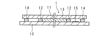
- FIG. 2 and 3 are cross-sectional views showing the main part of the liquid crystal panel 1.
- FIG. FIG. 2 shows a state where the liquid crystal panel 1 is not bent before assembling
- FIG. 3 shows a state where the liquid crystal panel 1 is bent after assembling.
- the liquid crystal panel 1 has two substrates 10 and 11 facing each other.
- the substrates 10 and 11 are made of glass or translucent resin. Therefore, the liquid crystal display device is a so-called transmissive liquid crystal display device.
- Driving elements such as pixel electrodes and switching elements are mounted on the opposing surface of the substrate 10, and an opposing electrode (not shown) is formed on the opposing surface of the substrate 11.
- a rectangular frame-shaped sealing body 12 is provided between the substrate 10 and the substrate 11.
- the sealing body 12 is formed along the periphery of the substrates 10 and 11.
- a liquid crystal 13 is sealed between the substrates 10 and 11 by a sealing body 12. That is, the liquid crystal 13 is sealed in a region formed by the sealing body 12 between the opposing surfaces of the substrates 10 and 11.
- the spacer 14 extends along the short side of the sealing body 12 outside the sealing body 12, that is, along the short side of the liquid crystal panel 1 on the short side of the liquid crystal panel 1. , 14 are formed. That is, the spacers 14 and 14 are disposed between the substrates 10 and 11 outside the sealing region of the liquid crystal 13 by the sealing body 12.
- a gate driver 15 to which the driving element is connected is disposed between the sealing body 12 and the spacer 14.
- the gate driver 15 is so-called monolithic and directly formed on the substrate 10.
- the gate driver 15 shown in FIGS. 2 and 3 is schematically shown, and the actual thickness of the gate driver 15 is about the same as the thickness of the driving element portion of the substrate 10.
- the liquid crystal panel 1 configured as described above is assembled in a liquid crystal display device as shown in FIG.
- the bezel 4 is in contact with the front surface of the liquid crystal panel 1 at a portion where the sealing body 12 and the spacer 14 are disposed.
- a force to return from the curvature is generated, so that the peripheral edge portion, in particular, the short side portion is pressed by the bezel 4. Thereby, a load is applied to the short side portion of the liquid crystal panel 1.
- the spacer 14 is provided in the short side part of the liquid crystal panel 1 assembled
- the part is in contact with the front surface of the liquid crystal panel 1.
- the load applied by the bezel 4 pressing the short side portion of the liquid crystal panel 1 is distributed to the sealing body 12 and the spacer 14. Accordingly, it is possible to prevent the liquid crystal panel 1 from being damaged due to the load being concentrated on the short side portion of the liquid crystal panel 1.
- a space between the sealing body 12 and the spacer 14 can be used as a formation region of the gate driver 15.
- the gate driver 15 By disposing the gate driver 15 between the sealing body 12 and the spacer 14, the space can be used without waste and the frame of the liquid crystal display device can be reduced.
- the formation of the gate driver 15 can be realized by monolithic formation as described above.
- the liquid crystal panel 1 may be a so-called reflective liquid crystal display device by assembling the liquid crystal panel 1 so that the substrate 10 does not have translucency and only the substrate 11 has translucency. .
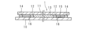
- FIG. 4 is a cross-sectional view showing a main part of the liquid crystal panel 1 assembled in the liquid crystal display device according to the second embodiment.
- the gate driver 15 shown in FIG. 4 is schematically shown in the same manner as in FIGS. 2 and 3 of the first embodiment, and the actual thickness of the gate driver 15 is about the same as the drive element portion of the substrate 10. It is thickness.
- a resin layer 16 is formed by encapsulating a resin between the sealing body 12 and the spacers 14 and 14.
- FIG. 5 is an explanatory diagram of the position of the resin layer 16.
- FIG. 5 shows the opposite surface of the substrate 10, and the resin layer 16 is formed in the region indicated by the oblique lines in FIG. 5.
- the liquid crystal panel 1 according to the second embodiment is bent in the same manner as in the first embodiment and assembled to the liquid crystal display device.
- the load applied to the short side portion of the liquid crystal panel 1 can be dispersed in the sealing body 12, the spacer 14, and the resin layer 16, so that the liquid crystal panel can be more reliably prevented from being damaged.
- FIG. 6 is a cross-sectional view showing a main part of the liquid crystal panel 1 assembled in the liquid crystal display device according to the third embodiment.
- symbol is attached
- an SOF (system on film) 18 including a flexible substrate 18 a and a gate driver 18 b mounted on the flexible substrate 18 a is provided on each substrate 10. It is connected to a terminal for inputting a signal to a driving element for driving the pixel.
- the SOF 18 is mounted outside the spacer 14, and the gate driver 18 is arranged outside the spacer 14.
- the liquid crystal panel 1 according to the third embodiment is bent in the same manner as in the first embodiment and assembled to the liquid crystal display device.
- the gate driver 18b since the gate driver 18b is mounted on the outside of the spacer 14 by the SOF 18, the gate driver 18b can be easily arranged.
- the gate driver 18b may be monolithically arranged and arranged outside the spacer on the opposite surface of the substrate 10.
- FIG. 7 is a cross-sectional view showing a main part of the liquid crystal panel 1 assembled in the liquid crystal display device according to the fourth embodiment.
- symbol is attached
- an SOF (system film) 18 including a flexible substrate 18a and a gate driver 18b mounted on the flexible substrate 18a is provided on each pixel on the substrate 10. Is connected to a terminal for inputting a signal to a driving element for driving the. Further, a resin is sealed between the sealing body 12 and the spacers 14 and 14, and a resin layer 19 is formed.
- the liquid crystal panel 1 according to the fourth embodiment is bent in the same manner as in the first embodiment and assembled to the liquid crystal display device.
- the load on the short side portion of the liquid crystal panel 1 can be dispersed in the sealing body 12, the spacer 14, and the resin layer 19, and the loss of the liquid crystal panel 1 can be prevented better.
- the spacers 14 may be formed continuously, or may be separated and provided in the form of dots. Furthermore, the spacer 14 may be provided on the long side instead of the short side of the liquid crystal panel. Further, the spacers 14 may be provided on both the short side and the long side.
Landscapes
- Physics & Mathematics (AREA)
- Nonlinear Science (AREA)
- Mathematical Physics (AREA)
- Chemical & Material Sciences (AREA)
- Crystallography & Structural Chemistry (AREA)
- General Physics & Mathematics (AREA)
- Optics & Photonics (AREA)
- Liquid Crystal (AREA)
Abstract
湾曲による液晶パネルの欠損を防止できる液晶表示装置を提供する。液晶パネル1は、正面の側が凸になるように湾曲している。液晶パネル1の基板10及び基板11間には、矩形枠状の封止体12が設けられている。封止体12は、基板10、11の周縁に沿って形成されている。また、基板10、11間において、封止体12により液晶13が封止されている。更に、基板10及び基板11間には、封止体12の外側に封止体12の短辺に沿って、即ち液晶パネル1の短辺側に液晶パネル1の短辺に沿って、スペーサ14、14が形成されている。ベゼル4は、封止体12及びスペーサ14が配された部分において、液晶パネル1の正面に接している。
Description
本発明は、正面に画像を表示する液晶パネルを備える液晶表示装置に関する。
液晶パネルを表示部として備える液晶表示装置は、液晶パネルの背面側にバックライトを配し、該バックライトからの照射光を液晶パネルにより変調して透過させ、液晶パネルの正面に画像を表示するように構成されている。液晶パネルは、相対する二枚の基板の対向面間に封止体で囲って形成された領域内に液晶を封止している。
液晶表示装置は、建造物内における円形断面の柱に沿わせて湾曲させて設置する場合がある。湾曲させた液晶表示装置において、液晶パネルは、正面の側が凸になるように湾曲させて組み付けられる。このとき、液晶パネルには、湾曲から元に戻る力が生じるので、側端部はベゼルによって押え込まれている。したがって、液晶パネルの側端部に負荷がかかり、液晶パネルに欠損が生じる場合がある。
ここで、特許文献1の液晶表示装置においては、封止体(メインシール)の外側に更に、樹脂の接合物を設けている。これにより、液晶パネルの封止体が設けられた部分に負荷がかかった場合に、封止体から二枚の基板が剥離することを防止している。
しかしながら、特許文献1に記載の液晶表示装置では、二枚の基板の封止体からの剥離は防止されるものの、ベゼルに押え込まれた液晶パネルの側端部に係る負荷による影響の対策としては不十分である。特に、液晶パネルの基板に割れ又はひびができる等の欠損が生じる虞がある。
本発明は、斯かる事情に鑑みてなされたものであり、その目的とするところは、湾曲による液晶パネルの欠損を防止できる液晶表示装置を提供することにある。
本発明に係る液晶表示装置は、相対する二枚の基板の対向面間に封止体で囲って形成された領域内に液晶を封止している液晶パネルと、該液晶パネルの正面の周縁部を覆う枠体とを備える液晶表示装置において、前記液晶パネルは、前記封止体による液晶の封止領域の外側で、前記二枚の基板間に配されたスペーサを有し、前記正面の側が凸になるように湾曲させて組み付けられており、前記枠体は、前記封止体及びスペーサが配された部分において、前記液晶パネルの正面に接していることを特徴とする。
本発明によれば、液晶パネルは、正面の側が凸になるように湾曲させて組み付けられており、枠体は、封止体及びスペーサが配された部分において、液晶パネルの正面に接している。したがって、枠体に押え込まれることで液晶パネルにかかる負荷は、封止体及びスペーサに分散される。これにより、液晶パネルにおいて一部に負荷が集中せず、湾曲による液晶パネルの欠損を防止できる。
本発明に係る液晶表示装置は、前記封止体及びスペーサ間に、ゲートドライバが配されていることを特徴とする。
本発明によれば、前記封止体及びスペーサ間にゲートドライバを配することにより、空間を無駄なく使用でき、液晶表示装置を狭額縁化できる。
本発明に係る液晶表示装置は、前記スペーサの外側にゲートドライバが配されていることを特徴とする。
本発明によれば、スペーサの外側にゲートドライバを配するので、ゲートドライバの配置を容易に行うことができる。
本発明に係る液晶表示装置は、前記封止体及びスペーサ間に、樹脂が封入されていることを特徴とする。
本発明によれば、液晶パネルにかかる負荷を、封止体、スペーサ及び封入された樹脂に分散し、液晶パネルの欠損をより良好に防止できる。
本発明によれば、湾曲による液晶パネルの欠損を防止できる。
以下、本発明に係る液晶表示装置についてその実施の形態を示す図面に基づいて詳述する。
(実施の形態1)
図1は、実施の形態1に係る液晶表示装置の断面図である。液晶表示装置は、正面に画像を表示する矩形の液晶パネル1と、該液晶パネル1の背面に光を照射するバックライト装置2とを備える。
(実施の形態1)
図1は、実施の形態1に係る液晶表示装置の断面図である。液晶表示装置は、正面に画像を表示する矩形の液晶パネル1と、該液晶パネル1の背面に光を照射するバックライト装置2とを備える。
バックライト装置2は、バックライトシャーシ20と、導光板21と、LED22とを備える。バックライトシャーシ20は、矩形の底板と、該底板の四辺から立ち上がる側板とを有し、一面が開口した浅底箱形をなす。
導光板21は、ガラス又は透光性を有する樹脂材料製の矩形の平板であり、矩形の反射シート24を介してバックライトシャーシ20の底板上に載置されている。また、導光板21は、一面がバックライトシャーシ20の開口側に露出している。
LED22は、バックライトシャーシ20の側板に取り付けられた基板23に実装されている。LED22は、発光面を導光板21の一側面に向けて実装されている。
液晶表示装置は、パネルシャーシ3と、ベゼル4と光学シート5とを更に備える。パネルシャーシ3は、矩形のフレームであり、枠形の前板と該前板の一面の外周縁から立ち上がる側板とを有する。パネルシャーシ3の前板は、バックライトシャーシ20の開口部の内側に延び、導光板21の周縁部に接し、該導光板21をバックライトシャーシ20の底板との間に挟持している。パネルシャーシ3は、側板をバックライトシャーシ20の側板の外側に被せてある。液晶パネル1は、周縁部が背面側から支持されるように、パネルシャーシ3の前板の他面に配されている。
ベゼル4は、矩形のフレームであり、枠形の前板と該前板の一面の外周縁から垂直に立ち上がる側板とを有する。ベゼル4は、側板をパネルシャーシ3の側板の外側に被せてあり、前板は液晶パネル1の正面の周縁部に接している。したがって、液晶パネル1は、ベゼル4の前板の一面とパネルシャーシ3の前板の他面とにより、周縁部を挟持されている。
光学シート5は、液晶パネル1と導光板21の隙間に配され、パネルシャーシ3の前板の内側に位置する。光学シート5は、光を拡散し、集束させる。
以上の如く構成された液晶表示装置は、例えば、建造物内の円形断面の柱に沿わせて設置される。液晶表示装置においてLED22から照射された光は、導光板21の一側面から入射し、導光板21内部を進行し、一面全体に分布して出射する。導光板21から出射した光は、光学シート5によって拡散及び集束され、液晶パネル1の背面に照射される。液晶パネル1は、入射光を変調して透過し、正面に画像を表示する。
ここで、図1に示すように、バックライトシャーシ20は、底板の一面の側が凸になるように湾曲している。パネルシャーシ3は、前板の他面の側が凸になるように湾曲し、ベゼル4は、前板の他面の側が凸になるように湾曲している。
導光板21は、バックライトシャーシ20及びパネルシャーシ3により挟まれ、バックライトシャーシ20の底板に沿って撓んでいる。液晶パネル1は、パネルシャーシ3とベゼル4との間に挟持され、パネルシャーシ3及びベゼル4に沿って撓んでいる。即ち液晶パネル1は、正面の側が凸になるように湾曲している。光学シート5は、導光板21に沿って撓んでいる。
導光板21は、バックライトシャーシ20及びパネルシャーシ3により挟まれ、バックライトシャーシ20の底板に沿って撓んでいる。液晶パネル1は、パネルシャーシ3とベゼル4との間に挟持され、パネルシャーシ3及びベゼル4に沿って撓んでいる。即ち液晶パネル1は、正面の側が凸になるように湾曲している。光学シート5は、導光板21に沿って撓んでいる。
図2及び図3は、液晶パネル1の要部を示す断面図である。図2は、液晶パネル1の組み付け前の湾曲させていない状態を示し、図3は、組み付け後の湾曲させた状態を示す。液晶パネル1は、相対する二枚の基板10、11を有する。基板10、11は、ガラス又は透光性を有する樹脂製である。したがって、液晶表示装置は、いわゆる透過型の液晶表示装置である。基板10の対向面には、画素電極及びスイッチング素子等の駆動素子(不図示)が実装され、基板11の対向面には対向電極(不図示)が形成されている。
基板10及び基板11間には、矩形枠状の封止体12が設けられている。封止体12は、基板10、11の周縁に沿って形成されている。また、基板10、11間において、封止体12により液晶13が封止されている。即ち、液晶13は、基板10、11の対向面間に封止体12で囲って形成された領域内に封止されている。更に、基板10及び基板11間には、封止体12の外側に封止体12の短辺に沿って、即ち液晶パネル1の短辺側に液晶パネル1の短辺に沿って、スペーサ14、14が形成されている。即ち、スペーサ14、14は、封止体12による液晶13の封止領域の外側で、基板10、11間に配されている。
基板10の対向面において、封止体12及びスペーサ14の間には、前記駆動素子が接続されたゲートドライバ15が配されている。ここでゲートドライバ15はいわゆるモノリシック化されて基板10上に直接形成されている。図2及び図3に示したゲートドライバ15は、模式的に示したものであり、ゲートドライバ15の実際の厚みは、基板10の前記駆動素子部分と同程度の厚みである。
以上の如く構成された液晶パネル1は、図3に示すように液晶表示装置に組み付けられている。ベゼル4は、封止体12及びスペーサ14が配された部分において、液晶パネル1の正面に接している。液晶パネル1には、湾曲から元に戻る力が生じるので、周縁部、特に短辺側部分がベゼル4によって押え込まれている。これにより、液晶パネル1の短辺側部分には、負荷がかかっている。
上記の構成によれば、正面の側が凸になるように湾曲させて組み付けられた液晶パネル1の短辺側部分にスペーサ14が設けられ、ベゼル4は、封止体12及びスペーサ14が配された部分において、液晶パネル1の正面に接している。これにより、ベゼル4が液晶パネル1の短辺側部分を押え込むことによりかかる負荷は封止体12及びスペーサ14に分散される。したがって、液晶パネル1の短辺側部分に負荷が集中することによる液晶パネル1の欠損を防止できる。
封止体12及びスペーサ14間はゲートドライバ15の形成領域として利用できる。ゲートドライバ15を封止体12及びスペーサ14の間に配することにより、空間を無駄なく使用でき、液晶表示装置の狭額縁化を図ることができる。ゲートドライバ15の形成は、上述の如く、モノリシック化により実現可能である。
なお、液晶パネル1を、基板10は透光性を有さず、基板11のみが透光性を有するように構成して組み付けることにより、液晶表示装置をいわゆる反射型の液晶表示装置としてもよい。
(実施の形態2)
図4は、実施の形態2に係る液晶表示装置に組み付けられる液晶パネル1の要部を示す断面図である。実施の形態2に係る液晶表示装置の構成について、実施の形態1と同様な構成については、同一の符号を付してその詳細な説明を省略する。図4に示したゲートドライバ15は、実施の形態1の図2及び図3同様、模式的に示したものであり、ゲートドライバ15の実際の厚みは、基板10の駆動素子部分と同程度の厚みである。
図4は、実施の形態2に係る液晶表示装置に組み付けられる液晶パネル1の要部を示す断面図である。実施の形態2に係る液晶表示装置の構成について、実施の形態1と同様な構成については、同一の符号を付してその詳細な説明を省略する。図4に示したゲートドライバ15は、実施の形態1の図2及び図3同様、模式的に示したものであり、ゲートドライバ15の実際の厚みは、基板10の駆動素子部分と同程度の厚みである。
実施の形態2においては、封止体12及びスペーサ14、14夫々の間に、樹脂を封入し、樹脂層16が形成されている。図5は、樹脂層16の位置の説明図である。図5は、基板10の対向面を示しており、図5の斜線に示す領域に樹脂層16が形成されている。実施の形態2に係る液晶パネル1は、実施の形態1と同様に湾曲させて、液晶表示装置に組み付けられる。
上記の構成によれば、液晶パネル1の短辺側部分にかかる負荷を封止体12、スペーサ14及び樹脂層16に分散し、液晶パネルの欠損をより良好に防止できる。
(実施の形態3)
図6は、実施の形態3に係る液晶表示装置に組み付けられる液晶パネル1の要部を示す断面図である。実施の形態3に係る液晶表示装置の構成について、実施の形態1と同様な構成については、同一の符号を付してその詳細な説明を省略する。
図6は、実施の形態3に係る液晶表示装置に組み付けられる液晶パネル1の要部を示す断面図である。実施の形態3に係る液晶表示装置の構成について、実施の形態1と同様な構成については、同一の符号を付してその詳細な説明を省略する。
実施の形態3においては、モノリシック化されたゲートドライバ15に代えて、フレキシブル基板18aと、該フレキシブル基板18aに搭載されたゲートドライバ18bとを備えるSOF(system on film)18が基板10上の各画素を駆動する駆動素子に信号を入力するための端子に接続されている。SOF18は、スペーサ14よりも外側に実装されており、ゲートドライバ18は、スペーサ14よりも外側に配されている。実施の形態3に係る液晶パネル1は、実施の形態1と同様に湾曲させて、液晶表示装置に組み付けられる。
上記の構成によれば、SOF18によりスペーサ14の外側にゲートドライバ18bが実装されているので、ゲートドライバ18bの配置を容易に行うことができる。なお、ゲートドライバ18bをモノリシック化し、基板10の対向面において、スペーサの外側に配してもよい。
(実施の形態4)
図7は、実施の形態4に係る液晶表示装置に組み付けられる液晶パネル1の要部を示す断面図である。実施の形態4に係る液晶表示装置の構成について、実施の形態1と同様な構成については、同一の符号を付してその詳細な説明を省略する。
図7は、実施の形態4に係る液晶表示装置に組み付けられる液晶パネル1の要部を示す断面図である。実施の形態4に係る液晶表示装置の構成について、実施の形態1と同様な構成については、同一の符号を付してその詳細な説明を省略する。
実施の形態4においては、モノリシック化されたゲートドライバ15に代えて、フレキシブル基板18aと、フレキシブル基板18aに搭載されたゲートドライバ18bとを備えるSOF(system on film)18が基板10上の各画素を駆動する駆動素子に信号を入力するための端子に接続されている。また、封止体12及びスペーサ14、14夫々の間に、樹脂が封入されており、樹脂層19が形成されている。実施の形態4に係る液晶パネル1は、実施の形態1と同様に湾曲させて、液晶表示装置に組み付けられる。
上記の構成によれば、液晶パネル1の短辺側部分に係る負荷を封止体12、スペーサ14及び樹脂層19に分散し、液晶パネル1の欠損をより良好に防止できる。
なお、上記の実施の形態1から実施の形態4において、スペーサ14は連続して形成されていてもよく、また、分離してドット状に設けられていてもよい。更に、スペーサ14を液晶パネルの短辺側でなく、長辺側に設けてもよい。また、スペーサ14を短辺側及び長辺側の両方に設けてもよい。
今回開示された実施の形態はすべての点で例示であって、制限的なものではないと考えられるべきである。本発明の範囲は、上記した意味ではなく、請求の範囲によって示され、請求の範囲と均等の意味及び範囲内でのすべての変更が含まれることが意図される。即ち、請求項に示した範囲で適宜変更した技術的手段を組み合わせて得られる実施形態も本発明の技術的範囲に含まれる。
1 液晶パネル
4 ベゼル(枠体)
10、11 基板
12 封止体
13 液晶
14 スペーサ
15、18b ゲートドライバ
16、19 樹脂
4 ベゼル(枠体)
10、11 基板
12 封止体
13 液晶
14 スペーサ
15、18b ゲートドライバ
16、19 樹脂
Claims (4)
- 相対する二枚の基板の対向面間に封止体で囲って形成された領域内に液晶を封止している液晶パネルと、該液晶パネルの正面の周縁部を覆う枠体とを備える液晶表示装置において、
前記液晶パネルは、前記封止体による液晶の封止領域の外側で、前記二枚の基板間に配されたスペーサを有し、前記正面の側が凸になるように湾曲させて組み付けられており、
前記枠体は、前記封止体及びスペーサが配された部分において、前記液晶パネルの正面に接している
ことを特徴とする液晶表示装置。 - 前記封止体及びスペーサ間に、ゲートドライバが配されていることを特徴とする請求項1に記載の液晶表示装置。
- 前記スペーサの外側にゲートドライバが配されていることを特徴とする請求項1に記載の液晶表示装置。
- 前記封止体及びスペーサ間に、樹脂が封入されていることを特徴とする請求項1から請求項3までのいずれか一つに記載の液晶表示装置。
Priority Applications (1)
| Application Number | Priority Date | Filing Date | Title |
|---|---|---|---|
| PCT/JP2015/080281 WO2017072864A1 (ja) | 2015-10-27 | 2015-10-27 | 液晶表示装置 |
Applications Claiming Priority (1)
| Application Number | Priority Date | Filing Date | Title |
|---|---|---|---|
| PCT/JP2015/080281 WO2017072864A1 (ja) | 2015-10-27 | 2015-10-27 | 液晶表示装置 |
Publications (1)
| Publication Number | Publication Date |
|---|---|
| WO2017072864A1 true WO2017072864A1 (ja) | 2017-05-04 |
Family
ID=58629928
Family Applications (1)
| Application Number | Title | Priority Date | Filing Date |
|---|---|---|---|
| PCT/JP2015/080281 Ceased WO2017072864A1 (ja) | 2015-10-27 | 2015-10-27 | 液晶表示装置 |
Country Status (1)
| Country | Link |
|---|---|
| WO (1) | WO2017072864A1 (ja) |
Citations (3)
| Publication number | Priority date | Publication date | Assignee | Title |
|---|---|---|---|---|
| JPH1073848A (ja) * | 1997-08-12 | 1998-03-17 | Seiko Epson Corp | 液晶パネル |
| JP2013109068A (ja) * | 2011-11-18 | 2013-06-06 | Mitsubishi Electric Corp | 液晶表示装置およびその製造方法 |
| JP2014063723A (ja) * | 2012-08-28 | 2014-04-10 | Semiconductor Energy Lab Co Ltd | 表示装置及びその作製方法 |
-
2015
- 2015-10-27 WO PCT/JP2015/080281 patent/WO2017072864A1/ja not_active Ceased
Patent Citations (3)
| Publication number | Priority date | Publication date | Assignee | Title |
|---|---|---|---|---|
| JPH1073848A (ja) * | 1997-08-12 | 1998-03-17 | Seiko Epson Corp | 液晶パネル |
| JP2013109068A (ja) * | 2011-11-18 | 2013-06-06 | Mitsubishi Electric Corp | 液晶表示装置およびその製造方法 |
| JP2014063723A (ja) * | 2012-08-28 | 2014-04-10 | Semiconductor Energy Lab Co Ltd | 表示装置及びその作製方法 |
Similar Documents
| Publication | Publication Date | Title |
|---|---|---|
| CN101387769B (zh) | 显示器件 | |
| US11726251B2 (en) | Display device having LCD with separate polarizing plates | |
| KR101130431B1 (ko) | 보호판 일체형 표시장치 | |
| JP5353606B2 (ja) | 保護板一体型表示装置 | |
| JP5254857B2 (ja) | 液晶表示装置 | |
| CN101231405B (zh) | 带触摸板的显示组件 | |
| JP5252431B2 (ja) | タッチパネル装置、電気光学装置及び電子機器 | |
| JP5216334B2 (ja) | 液晶表示装置 | |
| KR20100103364A (ko) | 보호판 일체형 표시장치 | |
| JP2013235145A (ja) | 表示装置 | |
| JP2008225414A (ja) | 液晶表示パネル | |
| WO2015177866A1 (ja) | 表示装置 | |
| JP2010085632A (ja) | 電気光学装置及びこれを備えた電子機器 | |
| CN105765448A (zh) | 显示装置以及显示装置的制造方法 | |
| JP2015022120A (ja) | 表示素子及びその製造方法 | |
| WO2016170620A1 (ja) | 光源装置及び表示装置 | |
| US9110323B2 (en) | Liquid crystal display device | |
| JP2011013511A (ja) | 保護板付き電子部材 | |
| JP2006163742A (ja) | タッチパネル付きの表示装置及びその製造方法 | |
| CN206990977U (zh) | 显示装置 | |
| JP2021047311A5 (ja) | ||
| TWI692660B (zh) | 反射式顯示裝置 | |
| KR20170124676A (ko) | 표시 장치 | |
| JP5218262B2 (ja) | 表示パネルとそれを用いる表示モジュール | |
| JP4065896B2 (ja) | 液晶表示パネル |
Legal Events
| Date | Code | Title | Description |
|---|---|---|---|
| 121 | Ep: the epo has been informed by wipo that ep was designated in this application |
Ref document number: 15907228 Country of ref document: EP Kind code of ref document: A1 |
|
| NENP | Non-entry into the national phase |
Ref country code: DE |
|
| 122 | Ep: pct application non-entry in european phase |
Ref document number: 15907228 Country of ref document: EP Kind code of ref document: A1 |
|
| NENP | Non-entry into the national phase |
Ref country code: JP |