WO2017056321A1 - 樹脂付リードフレームおよびその製造方法、ならびにledパッケージおよびその製造方法 - Google Patents
樹脂付リードフレームおよびその製造方法、ならびにledパッケージおよびその製造方法 Download PDFInfo
- Publication number
- WO2017056321A1 WO2017056321A1 PCT/JP2015/078093 JP2015078093W WO2017056321A1 WO 2017056321 A1 WO2017056321 A1 WO 2017056321A1 JP 2015078093 W JP2015078093 W JP 2015078093W WO 2017056321 A1 WO2017056321 A1 WO 2017056321A1
- Authority
- WO
- WIPO (PCT)
- Prior art keywords
- lead frame
- resin
- metal portion
- reflective resin
- reflective
- Prior art date
- Legal status (The legal status is an assumption and is not a legal conclusion. Google has not performed a legal analysis and makes no representation as to the accuracy of the status listed.)
- Ceased
Links
Images








Classifications
-
- H—ELECTRICITY
- H10—SEMICONDUCTOR DEVICES; ELECTRIC SOLID-STATE DEVICES NOT OTHERWISE PROVIDED FOR
- H10H—INORGANIC LIGHT-EMITTING SEMICONDUCTOR DEVICES HAVING POTENTIAL BARRIERS
- H10H20/00—Individual inorganic light-emitting semiconductor devices having potential barriers, e.g. light-emitting diodes [LED]
- H10H20/80—Constructional details
- H10H20/85—Packages
-
- H—ELECTRICITY
- H10—SEMICONDUCTOR DEVICES; ELECTRIC SOLID-STATE DEVICES NOT OTHERWISE PROVIDED FOR
- H10W—GENERIC PACKAGES, INTERCONNECTIONS, CONNECTORS OR OTHER CONSTRUCTIONAL DETAILS OF DEVICES COVERED BY CLASS H10
- H10W72/00—Interconnections or connectors in packages
- H10W72/01—Manufacture or treatment
- H10W72/0198—Manufacture or treatment batch processes
-
- H—ELECTRICITY
- H10—SEMICONDUCTOR DEVICES; ELECTRIC SOLID-STATE DEVICES NOT OTHERWISE PROVIDED FOR
- H10W—GENERIC PACKAGES, INTERCONNECTIONS, CONNECTORS OR OTHER CONSTRUCTIONAL DETAILS OF DEVICES COVERED BY CLASS H10
- H10W90/00—Package configurations
- H10W90/701—Package configurations characterised by the relative positions of pads or connectors relative to package parts
- H10W90/751—Package configurations characterised by the relative positions of pads or connectors relative to package parts of bond wires
- H10W90/756—Package configurations characterised by the relative positions of pads or connectors relative to package parts of bond wires between a chip and a stacked lead frame, conducting package substrate or heat sink
Definitions
- the present invention relates to a lead frame with resin and a manufacturing method thereof, and an LED package and a manufacturing method thereof.
- LED light emitting diode
- Some of such lighting devices include a semiconductor device manufactured by mounting LED elements on a lead frame.
- an SON type (SON package) has been developed from the viewpoint of heat dissipation and the like.
- a reflective resin (reflector) for reflecting light from the LED element is provided.
- the LED element and the bonding wire are sealed with a sealing resin that protects them (see, for example, Patent Document 1).
- the area of the back surface of the die pad and the lead portion is made larger from the viewpoint of heat dissipation as compared with a general semiconductor package. For this reason, in the LED package, when the package is solder-mounted on the printed board, the amount of solder used is larger than that of a general semiconductor package. For this reason, in the LED package, a volatile component of the solder flux is likely to be caught in the solder on the back surface of the package, and as a result, there is a problem that voids are easily generated in the solder. When a void is generated in the solder, there is a problem that heat is not easily released from the back surface of the die pad or the lead portion in the LED package.
- noble metal plating is applied to the lead frame, and the adhesion between the noble metal plating and the reflective resin is poor due to a large difference in thermal expansion coefficient. For this reason, hydrogen sulfide or moisture in the air enters from the interface between the reflective resin and the lead frame, and this reacts with the noble metal plating inside the LED package, so that the noble metal plating layer changes color, and the reflectance and color of the LED package. May adversely affect taste.
- Patent Document 2 by forming a noble metal plating layer projecting in an overhang shape on the resin portion, the entrance of the interface formed between the resin portion and the lead frame is blocked, and the LED package It tries to prevent moisture from entering inside.
- Patent Document 3 discloses that the side surface of the lead frame with Ag plating in contact with the resin portion is roughened by a laser to increase the adhesion area between the resin portion and the Ag plating surface, so that the sealing resin in the LED package is outside the LED package. It is possible to prevent leakage into the cavity and to prevent sulfide penetration into the cavity.
- Patent Documents 2 and 3 are techniques that involve an increase in manufacturing cost and an increase in the number of processes, there is a problem that the manufacturing method becomes complicated. That is, in Patent Document 2, when the thickness of the noble metal plating layer for closing the interface entrance formed between the resin portion and the lead frame is increased, there is a problem that the manufacturing cost is higher than that of the conventional manufacturing method. Moreover, in patent document 3, since a part of lead frame with Ag plating is roughened with a laser, there exists a problem that the noble metal detached
- the present invention has been made in consideration of the above points, and is capable of preventing the generation of voids in the solder on the back surface of the LED package, the resin-attached lead frame, the manufacturing method thereof, the LED package, and It aims at providing the manufacturing method.
- the present invention provides a resin-attached resin that can prevent a fluid such as moisture from entering from the interface between the lead frame and the reflective resin without increasing the manufacturing cost and using a complicated manufacturing method.
- An object is to provide a lead frame and a manufacturing method thereof, and an LED package and a manufacturing method thereof.
- the present invention relates to a lead frame with resin, wherein the lead frame includes a first metal portion and a second metal portion provided apart from the first metal portion, the first metal portion, and the second metal portion. And a reflective resin integrated with a lead frame, and at least the first metal portion or the second metal portion is formed with an outer lead portion, and among the reflective resins, A lead frame with resin, wherein a plurality of protrusions are formed on a surface side of the lead frame on which the outer lead portion is formed.
- the present invention is the lead frame with resin, wherein each protrusion has a height of 10 ⁇ m to 30 ⁇ m and a width of 10 ⁇ m to 100 ⁇ m.
- the present invention is the lead frame with resin, wherein the ratio of the area of the plurality of protrusions to the unit area of the back surface of the reflective resin is 10% to 50%.
- the present invention is the lead frame with resin, wherein the plurality of protrusions are provided in a region surrounding the periphery of the first metal portion or a region surrounding the periphery of the second metal portion.
- the present invention is the lead frame with resin, wherein the plurality of protrusions are provided in a region along the outer shape of the mounting surface of the LED package.
- the present invention is the lead frame with resin, wherein the plurality of protrusions are irregularly arranged.
- the present invention is the lead frame with resin, wherein the at least one protrusion partially covers the periphery of the back surface of the first metal portion or the periphery of the back surface of the second metal portion.
- the present invention provides an LED package having a lead frame having a first metal portion and a second metal portion spaced apart from the first metal portion, and mounted on the first metal portion of the lead frame.
- An LED element a conductive portion that electrically connects the LED element and the second metal portion of the lead frame; a reflective resin that is provided in the lead frame and has a recess that accommodates the LED element;
- An LED package comprising: a sealing resin filled in the recess of resin, wherein a plurality of protrusions are formed on the back surface of the reflective resin.
- the present invention provides a method of manufacturing a lead frame with a resin, the step of preparing a lead frame including a first metal portion and the second metal portion provided apart from the first metal portion, and the lead frame And a step of providing a reflective resin on the lead frame, wherein a plurality of protrusions are formed on the back surface of the reflective resin.
- the reflective resin in the step of providing a reflective resin on the lead frame, is molded using a mold made of sintered metal, and the mold has a plurality of holes corresponding to the plurality of protrusions.
- the present invention further comprises a step of providing a plating layer so as to cover a region of the lead frame where the reflective resin is not provided after the reflective resin is provided on the lead frame. It is a manufacturing method of a lead frame.
- the present invention provides a method for manufacturing an LED package, the step of preparing a lead frame with resin, the step of mounting an LED element on the first metal portion of the lead frame with resin, the LED element and the lead frame with resin.
- a method for manufacturing an LED package comprising: a step of connecting the second metal portion to the conductive portion, and a step of sealing the LED element and the conductive portion with a sealing resin.
- the volatile components of the solder flux can be released through the protrusions, and voids are generated in the solder on the back surface of the LED package. Can be prevented.
- a lead frame with a resin in a lead frame with a resin, a lead frame having a first metal portion, a second metal portion provided apart from the first metal portion, and a reflective resin provided on the lead frame.
- the lead frame with resin is characterized in that the contact angle of the outer surface of the lead frame to pure water is 100 ° or more, and the contact angle of the outer surface of the reflective resin to pure water is 100 ° or more.
- a region of the lead frame where the reflective resin is not provided is covered with a plating portion, and a contact angle of the lead frame is a contact angle of the plating portion.
- the present invention is characterized in that a gap portion where the reflection resin and the lead frame are separated is formed at an interface between the reflection resin and the lead frame, and the plating portion is filled in the gap portion.
- This is a lead frame with resin.
- the present invention is the lead frame with resin, wherein a water repellent film is formed on each of the outer surface of the lead frame and the outer surface of the reflective resin.
- the present invention provides an LED package having a lead frame having a first metal portion and a second metal portion spaced apart from the first metal portion, and mounted on the first metal portion of the lead frame.
- An LED element a conductive portion that electrically connects the LED element and the second metal portion of the lead frame; a reflective resin that is provided in the lead frame and has a recess that accommodates the LED element;
- a sealing resin filled in the concave portion of the resin, the contact angle of the outer surface of the lead frame with respect to pure water is 100 ° or more, and the contact angle of the outer surface of the reflective resin with respect to pure water is 100 ° or more.
- the present invention provides a method of manufacturing a lead frame with a resin, the step of preparing a lead frame including a first metal portion and the second metal portion provided apart from the first metal portion, and the lead frame And a step of providing a reflection resin on the outer surface of the lead frame with respect to pure water, and a contact angle of the outer surface of the reflection resin with respect to pure water is 100 ° or more.
- This is a manufacturing method of a lead frame with resin.
- the present invention is a method for manufacturing a lead frame with a resin, wherein a step of increasing water repellency of the lead frame and the reflective resin is provided after the step of providing a reflective resin on the lead frame.
- the present invention is a method for manufacturing a lead frame with a resin, wherein the step of increasing the water repellency of the lead frame and the reflective resin is a step of heating the lead frame and the reflective resin.
- the present invention is a method for manufacturing a lead frame with resin, wherein the lead frame and the reflective resin are heated at a temperature of 100 ° C. to 250 ° C.
- the step of increasing the water repellency of the lead frame and the reflective resin is a step of forming a water repellent film on the outer surface of the lead frame and the outer surface of the reflective resin. It is a manufacturing method.
- the present invention provides a method for manufacturing an LED package, the step of preparing the lead frame with resin, the step of mounting an LED element on the first metal portion of the lead frame with resin, the LED element and the lead with resin.
- An LED package manufacturing method comprising: a step of connecting the second metal portion of the frame with a conductive portion; and a step of sealing the LED element and the conductive portion with a sealing resin.
- a lead frame with a resin a lead frame having a first metal portion, a second metal portion provided apart from the first metal portion, and a reflective resin provided on the lead frame.
- the contact angle of the outer surface of the lead frame to pure water is 95 ° to 110 °
- the contact angle of the outer surface of the reflective resin to pure water is 100 ° to 110 °. It is a manufacturing method of an LED package.
- the present invention it is possible to prevent a fluid such as moisture from entering from the interface between the lead frame and the reflective resin without increasing the manufacturing cost and using a complicated manufacturing method.
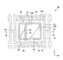
- FIG. 1 is a plan view showing a lead frame with resin according to a first embodiment of the present invention.
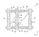
- FIG. 2 is a bottom view showing the lead frame with resin according to the first embodiment of the present invention.
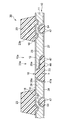
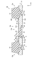
- FIG. 3 is a cross-sectional view showing a lead frame with resin according to the first embodiment of the present invention (cross-sectional view taken along line III-III in FIG. 1).
- FIG. 4 is a bottom view showing the lead frame with resin, and is a view for explaining a region where a protrusion is provided.
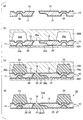
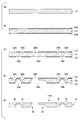
- FIGS. 7 (a) to 7 (f) are cross-sectional views showing a method of manufacturing a lead frame with resin according to the first embodiment of the present invention.
- FIGS. 8A to 8D are cross-sectional views showing a method for manufacturing a resin-added lead frame according to the first embodiment of the present invention.
- FIGS. 9A to 9E are cross-sectional views showing a method for manufacturing an LED package according to the first embodiment of the present invention.
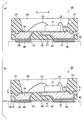
- FIGS. 10A and 10B are views showing an operation when the LED package is mounted on the wiring board.
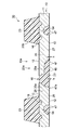
- FIG. 11 is a cross-sectional view showing a lead frame with resin according to a modification of the first embodiment.
- FIG. 12 is a cross-sectional view showing an LED package according to a modification of the first embodiment.
- FIG. 13 is a plan view showing a lead frame with resin according to the second embodiment of the present invention.
- FIG. 14 is a cross-sectional view showing a resin-attached lead frame according to the second embodiment of the present invention (cross-sectional view taken along line XIV-XIV in FIG. 13).
- FIG. 15 is a plan view showing an LED package according to a second embodiment of the present invention.
- FIG. 16 is a cross-sectional view showing the LED package according to the second embodiment of the present invention (cross-sectional view taken along line XVI-XVI in FIG. 15).
- FIG. 17 is a cross-sectional view showing the LED package according to the second embodiment of the present invention (cross-sectional view taken along line XVII-XVII in FIG. 15).
- 18 (a) to 18 (e) are cross-sectional views showing a method of manufacturing a lead frame with resin according to the second embodiment of the present invention.
- 19 (a) to 19 (e) are cross-sectional views showing a method of manufacturing a lead frame with resin according to the second embodiment of the present invention.
- 20 (a) to 20 (e) are cross-sectional views showing a method for manufacturing an LED package according to a second embodiment of the present invention.
- the “front surface” refers to the surface on the light emitting surface side of the LED package (upper surface in FIG. 3), and the “rear surface” refers to the surface on the mounting surface side of the LED package (lower surface in FIG. 3).
- the “back surface” of the lead frame is a surface on which a die pad used for connecting the LED package and an external wiring board and an outer lead portion of the lead portion are formed.
- the “back surface” of the reflective resin is a surface on the surface side where the outer lead portion of the lead frame is formed.
- FIGS. 1 to 4 a description will be given of a schematic of a lead frame with a resin according to the present embodiment.
- the lead frame 30 with resin shown in FIGS. 1 to 3 is used for manufacturing the LED package 20 (see FIGS. 5 and 6).
- a lead frame 30 with resin includes a lead frame 10 and a reflective resin (reflector) 23 provided on the lead frame 10.
- the lead frame 10 includes a plurality of unit lead frames 10a each of which corresponds to one LED package 20.
- a region included in each unit lead frame 10a is indicated by a rectangular two-dot chain line.
- Each lead frame 10 includes a die pad (first metal portion) 25 on which an LED element 21 (described later) is mounted, and a lead portion (second metal portion) 26 provided apart from the die pad 25. .
- the die pad 25 and the lead part 26 each have a substantially rectangular shape in plan, and each side of the die pad 25 and the lead part 26 extends in parallel to either the X direction or the Y direction.
- the X direction means a direction parallel to the direction in which the die pad 25 and the lead portion 26 are arranged in each unit lead frame 10a
- the Y direction is orthogonal to the X direction in a plane. The direction.
- An opening region 16 is formed between the die pad 25 and the lead portion 26, and after dicing (see FIG. 9D), the die pad 25 and the lead portion 26 are electrically insulated from each other. It has become.
- the center side portion 25 a located on the lead portion 26 side of the die pad 25 is half-etched from the back surface direction thereof, whereby the material thickness of the lead frame 10 (that is, a metal substrate 31 described later). Thickness).
- a center side portion 26a located on the die pad 25 side in the lead portion 26 is half-etched from the back surface direction so that it is thinner than the thickness of the material of the lead frame 10.
- Half-etching means that the material to be etched is etched halfway in the thickness direction.
- each unit lead frame 10a are connected to the lead portions 26 in other unit lead frames 10a adjacent to the Y direction plus side and the Y direction minus side in FIG.
- the parts 52 are connected.
- the die pad 25 in each unit lead frame 10a is connected to the die pad 25 in another unit lead frame 10a adjacent to the Y direction plus side and the Y direction minus side in FIG. .
- each unit lead frame 10a is connected to the lead part 26 in another unit lead frame 10a adjacent to the X direction plus side in FIG. Furthermore, the lead part 26 in each unit lead frame 10a is connected to the die pad 25 in the other unit lead frame 10a adjacent to the minus side in the X direction in FIG.
- the lead connecting portion 52, the die pad connecting portion 53, and the unit lead frame connecting portion 54 are each half-etched from the back surface side so that the thickness of the material of the lead frame 10 (that is, the thickness of the metal substrate 31 described later) is thinner. Is formed.
- first outer lead portion 27 is formed on the back surface of the die pad 25, and a second outer lead portion 28 is formed on the back surface of the lead portion 26.
- the first outer lead portion 27 and the second outer lead portion 28 are used when connecting the LED package 20 and the external wiring board 45 (see FIGS. 10A and 10B), respectively.
- a groove 18 is provided in a region covered with the reflective resin 23 on the surface of the lead frame 10.
- the planar shape of the groove 18 extends in an annular shape except for the opening region 16 and is substantially rectangular.
- the present invention is not limited thereto, and the planar shape of the groove 18 may be substantially oval or substantially racetrack.
- the cross-sectional shape of the groove 18 is a concave shape, and the adhesive resin 23 enters the groove 18 to enhance the adhesion between the lead frame 10 and the reflective resin 23.
- the reflection resin 23 is provided on the die pad 25 and the lead part 26 on the surface of the lead frame 10. Further, the reflective resin 23 surrounds the die pad 25 and the lead portion 26. Further, the reflective resin 23 is formed by the opening region 16 between the die pad 25 and the lead portion 26, the back surface of the lead connecting portion 52, the back surface of the die pad connecting portion 53, the back surface of the unit lead frame connecting portion 54, and the die pad 25 and the lead portion. The back surfaces of the central portions 25a and 26a of the 26 are also filled.
- the reflective resin 23 is integrated with the lead frame 10 and has a recess 23a for accommodating the LED element 21 (described later).
- the planar shape of the recess 23a may be, for example, a rectangular shape, a rounded rectangular shape, a circular shape, an elliptical shape, an oval shape, or a race track shape.
- the reflective resin 23 has an inclined surface 23b formed so as to expand from the back surface side to the front surface side.
- a plurality of (many) protrusions 47 are formed on the back surface of the reflective resin 23.
- the protrusion 47 is formed over the entire back surface of the reflective resin 23.
- a portion of the back surface of the reflective resin 23 excluding the protrusions 47 is substantially flat, and a gap 48 between which the volatile components of the solder flux can be released as described later. Is formed.
- the plurality of protrusions 47 are arranged so that their shapes, sizes, intervals, and densities are irregular.
- the solder flux gas can be released in various directions when performing reflow soldering.
- the present invention is not limited to this, and a plurality of protrusions 47 may be regularly arranged.
- the shape of the back surface of the reflective resin 23 can be made the same between the unit lead frames 10a, so that variation in characteristics between the LED packages 20 can be reduced.
- Each protrusion 47 has a height h (see FIG. 3) of 10 ⁇ m to 30 ⁇ m (refers to 10 ⁇ m or more and 30 ⁇ m or less; the same applies hereinafter) and a width w (see FIG. 2) of 10 ⁇ m to 100 ⁇ m.
- the height h of each projection 47 refers to the distance between the most protruding portion of each projection 47 and the flat portion of the back surface of the reflective resin 23 without the projection 47.
- the width w of each protrusion 47 is the distance between the widest portions of the protrusions 47. In each figure, the size of each protrusion 47 is exaggerated. Further, when the reflective resin 23 is provided after providing the plating layer 12 (pre-plating, see FIG.
- the protrusion 47 on the back surface of the first outer lead portion 27 and the back surface of the second outer lead portion 28 is 10 ⁇ m to 30 ⁇ m as described above.
- the first outer lead portion 27 and the second outer lead portion 28 of the protrusion 47 are provided. Since the thickness of the plating layer 12 is about 1 to 5 ⁇ m, the height of the surface is 5 ⁇ m to 29 ⁇ m by subtracting the thickness of the plating layer 12 from 10 ⁇ m to 30 ⁇ m.
- each protrusion 47 By setting the height h of each protrusion 47 to 10 ⁇ m or more, the LED package 20 and the wiring board can be used even when the LED package 20 is inclined at an angle during reflow soldering (see FIG. 10B). Since a certain gap can be ensured with respect to 45, the volatile component (gas) of the solder flux can be surely released from the gap 48 between the protrusions 47. Further, since the height h of each protrusion 47 is set to 30 ⁇ m or less, the height of each protrusion 47 becomes lower than the height of the solder 43 that connects the LED package 20 and the wiring board 45, so that the LED package 20 and the wiring The substrate 45 can be securely connected by the solder 43.
- each protrusion 47 by setting the width w of each protrusion 47 to 10 ⁇ m or more, even if the LED package 20 is inclined obliquely during reflow soldering (see FIG. 10B), the LED package 20 and the wiring A certain gap can be secured between the substrate 45 and the solder flux gas can be surely released. Further, by setting the width w of each protrusion 47 to 100 ⁇ m or less, a gap 48 having a predetermined size can be secured between the protrusions 47, and when performing reflow soldering, the solder flux from the gap 48 is used. The gas can be surely released.
- the ratio of the area of the plurality of protrusions 47 to the unit area of the back surface of the reflective resin 23 is preferably 10% to 50%.
- the ratio is the total area of the protrusions 47 existing in the region with respect to the area of the region where the plurality of protrusions 47 are formed in the back surface of the reflective resin 23 (the portion exposed on the back surface side).
- the ratio of the total area of the plurality of protrusions 47 to the total area of the back surface of the reflective resin 23 is referred to.
- the ratio By setting the ratio to 10% or more, a certain gap is ensured between the LED package 20 and the wiring board 45 even when the LED package 20 is inclined during reflow soldering. Therefore, the solder flux gas can be easily released. Further, by setting the ratio to 50% or less, a gap 48 having a predetermined size can be secured between the protrusions 47. Therefore, when performing reflow soldering, the solder flux gas is emitted from the gap 48. Can be surely escaped.
- the plurality of protrusions 47 are formed over the entire back surface of the reflective resin 23, but are not limited thereto.
- the plurality of protrusions 47 may be provided in a region A 1 surrounding the die pad 25 and / or a region A 2 surrounding the lead portion 26.
- the plurality of protrusions 47 are formed on the first outer lead portion 27 and the second outer lead portion 28 by projecting from the first outer lead portion 27 and the second outer lead portion 28.
- the plating layer 12 (described later) is prevented from coming into direct contact with an external member. Thereby, it is possible to prevent the plating layer 12 from being damaged.
- a plurality of projections 47 may be provided in a region A 3 along the outline of the mounting surface of the unit lead frame 10a (LED package 20).
- LED package 20 is inclined obliquely when viewed from the side (see FIG. 10B)
- a constant gap is provided between the LED package 20 and the wiring board. Therefore, the solder flux gas can be surely released.
- At least one of the plurality of protrusions 47 may partially cover the periphery of the back surface of the die pad 25 or the periphery of the back surface of the lead portion 26 (see the protrusions 47a in FIGS. 2 and 3). In this case, since the protrusion 47a restricts the die pad 25 or the lead part 26 from moving downward, it is possible to prevent a problem that the die pad 25 or the lead part 26 falls off to the back side.
- the protrusion 47 is not provided on the surface side of the reflective resin 23. By not providing the protrusion 47 on the surface side of the reflective resin 23, it is possible to prevent a problem that light from the LED element 21 (described later) is reflected by the protrusion 47 in an unexpected direction.
- the lead frame 10 includes a lead frame main body 11 and a plating layer 12 formed on the lead frame main body 11.
- the lead frame body 11 is made of a metal plate.
- the material of the metal plate constituting the lead frame body 11 include copper, copper alloy, 42 alloy (Ni 42% Fe alloy), iron alloy (stainless steel, FeNi), aluminum, and the like.
- the thickness of the lead frame main body 11 is preferably 0.05 mm to 0.5 mm, although it depends on the configuration of the LED package 20.
- the plating layer 12 is provided so as to cover the entire front and back surfaces of the lead frame body 11. Of these, the plating layer 12 on the surface side is exposed from a portion of the die pad 25 and the lead portion 26 that is not covered with the reflective resin 23.
- the plating layer 12 mainly functions as a reflection layer for reflecting light from the LED element 21.
- the plating layer 12 on the back surface side is exposed from a portion of the die pad 25 and the lead portion 26 that is not covered with the reflective resin 23, specifically, the first outer lead portion 27 and the second outer lead portion 28. is doing.
- the plating layer 12 on the back side plays a role of improving the adhesion with the solder.
- the lower surface of the plating layer 12 on the back surface side and the lower surface of the reflective resin 23 on the back surface side are located on the same plane.
- the present invention is not limited to this, and the lower surface of the plating layer 12 on the back surface side may protrude downward by, for example, about 2 ⁇ m to 3 ⁇ m from the lower surface of the reflective resin 23 on the back surface side. In either case, the protrusion 47 protrudes below the lower surface of the plating layer 12 on the back surface side. As a result, the plating layer 12 on the back surface side is prevented from coming into direct contact with an external member, thereby preventing the plating layer 12 from being damaged.
- the plating layer 12 may be made of, for example, single layer plating of silver, a silver alloy, gold or an alloy thereof, a platinum group, copper or an alloy thereof, or aluminum.
- the thickness of the plating layer 12 is preferably 0.5 ⁇ m to 30 ⁇ m.
- the plating layer 12 may be composed of multilayer plating.
- the plating layer 12 may include a base plating layer and a noble metal plating layer laminated on the base plating layer.
- the base plating layer include copper, nickel, palladium, or an electrolytic plating layer in which a plurality of these are stacked.
- the thickness of the base plating layer may be, for example, 0.1 ⁇ m to 15 ⁇ m, and more preferably 2 ⁇ m to 10 ⁇ m.
- the noble metal plating layer include silver, a silver alloy, gold and its alloys, a platinum group, copper and its alloys, and a vapor phase plating layer of aluminum.
- the thickness of the noble metal plating layer may be, for example, 2 ⁇ m to 15 ⁇ m, and more preferably 3 ⁇ m to 7 ⁇ m.
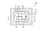
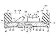
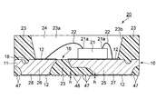
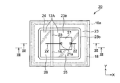
- FIGS. 5 and 6 are a sectional view and a plan view, respectively, showing an LED package (SON type).
- the LED package (semiconductor device) 20 includes a lead frame 10, an LED element 21 placed on a die pad 25 of the lead frame 10, an LED element 21, a die pad 25, and a lead part 26. And a bonding wire (conductive portion) 22 for electrically connecting the two.
- a reflective resin 23 having a recess 23 a is provided so as to surround the LED element 21.
- the reflective resin 23 is integrated with the lead frame 10.
- a plurality of (many) protrusions 47 are formed on the back surface of the reflective resin 23.
- the LED element 21 and the bonding wire 22 are sealed with a translucent sealing resin 24. This sealing resin 24 is filled in the recess 23 a of the reflective resin 23.
- the LED element 21 selects an emission wavelength ranging from ultraviolet light to infrared light by appropriately selecting a material made of a compound semiconductor single crystal such as GaP, GaAs, GaAlAs, GaAsP, AlInGaP, or InGaN as a light emitting layer. Can do. As such an LED element 21, those conventionally used in general can be used.
- the LED element 21 is fixedly mounted on the die pad 25 in the recess 23a of the reflective resin 23 by solder or die bonding paste.
- solder or die bonding paste it is possible to select a die bonding paste made of an epoxy resin or a silicone resin having light resistance.
- the bonding wire 22 is made of a material having good conductivity such as gold, and one end thereof is connected to each terminal portion 21a of the LED element 21 and the other end is connected to the die pad 25 and the lead portion 26, respectively. 5 and 6, one of the pair of terminal portions 21 a provided on the surface of the LED element 21 and the die pad 25 are electrically connected by the bonding wire 22, but are not limited thereto.
- the terminal portion 21a may be provided on the back surface of the LED element 21, and the terminal portion 21a and the die pad 25 may be electrically connected via solder.
- the reflection resin 23 is formed by, for example, transfer molding or injection molding of a thermoplastic resin or a thermosetting resin on the lead frame 10.
- the shape of the reflective resin 23 can be variously realized by designing a mold used for transfer molding or injection molding.
- the entire shape of the reflective resin 23 may be a rectangular parallelepiped as shown in FIGS. 5 and 6, or may be a cylindrical shape or a cone shape.
- the bottom surface of the recess 23a is not limited to a rectangular shape, an oval shape, or a racetrack shape, and may be a circle, an ellipse, a polygon, or the like.
- the cross-sectional shape of the inclined surface 23b of the recessed part 23a may be comprised from the straight line like FIG. 6, or may be comprised from the curve.
- the color of the reflective resin 23 may be beige or black in addition to white.
- thermoplastic resin or thermosetting resin used for the reflective resin 23 it is desirable to select a resin having excellent heat resistance, weather resistance and mechanical strength.
- thermoplastic resin polyamide, polyphthalamide, polyphenylene sulfide, liquid crystal polymer, polyethersulfone, polybutylene terephthalate, polyetherimide, or the like can be used.
- thermosetting resin a silicone resin, an epoxy resin, polyurethane, or the like can be used.
- titanium dioxide, zirconium dioxide, potassium titanate, aluminum nitride, and boron nitride as a light reflecting agent in these resins, the bottom surface and the side wall of the recess 23a can emit light from the light emitting element.
- thermoplastic resin which consists of polyolefins, such as polymethylpentene and a polypropylene.
- the heat resistance can be improved while maintaining the moldability of the thermoplastic resin.
- the sealing resin 24 it is desirable to select a material having a high light transmittance and a high refractive index at the emission wavelength of the LED package 20 in order to improve the light extraction efficiency. Therefore, it is possible to select an epoxy resin or a silicone resin as a resin that satisfies the characteristics of high heat resistance, weather resistance, and mechanical strength.
- the sealing resin 24 is preferably made of a silicone resin having high weather resistance because the sealing resin 24 is exposed to strong light.
- FIGS. 7 (a)-(f) and FIGS. 8 (a)-(d) are cross-sectional views showing a method of manufacturing the lead frame 30 with resin according to the present embodiment, each corresponding to the cross section shown in FIG. ing.
- a flat metal substrate 31 is prepared.
- a metal substrate made of copper, copper alloy, 42 alloy (Ni 42% Fe alloy), iron alloy (stainless steel, FeNi), aluminum or the like can be used.
- photosensitive resists 32a and 33a are applied to the entire front and back surfaces of the metal substrate 31, respectively, and dried (FIG. 7B).
- photosensitive resists 32a and 33a conventionally known resists can be used.
- the metal substrate 31 is exposed through a photomask and developed to form etching resist layers 32 and 33 having desired openings 32b and 33b (FIG. 7C).
- Corrosion liquid can be suitably selected according to the material of the metal substrate 31 to be used. For example, when copper is used as the metal substrate 31, a ferric chloride aqueous solution is usually used and spray etching can be performed from both surfaces of the metal substrate 31.
- the etching resist layers 32 and 33 are peeled and removed, whereby the lead frame 10 (lead frame including a plurality of unit lead frames including the die pad 25 and the lead portion 26 provided apart from the die pad 25).
- the main body 11 is obtained (FIG. 7 (e)).
- a metal for example, silver
- the plating layer 12 is formed on the entire surface including the front and back surfaces of the lead frame main body 11. Is formed (FIG. 7F).
- the lead frame main body 11 is sequentially subjected to, for example, an electrolytic degreasing step, a pickling step, a chemical polishing step, a copper strike step, a water washing step, a neutral degreasing step, a cyan washing step, and a silver plating step.
- the plating layer 12 is formed.
- examples of the plating solution for electrolytic plating used in the silver plating step include a silver plating solution mainly composed of silver cyanide.
- a water washing process is appropriately added between the processes as necessary.
- the plating layer 12 may be formed only on a part of the lead frame main body 11 by interposing a patterning step in the middle of the above steps.
- the lead frame 10 (FIG. 8A) obtained in this manner is sandwiched between a lower mold 35A and an upper mold 35B of an injection molding machine or a transfer molding machine (not shown). (FIG. 8B). A space 35a corresponding to the shape of the reflective resin 23 is formed in the upper mold 35B.
- a plurality of holes 35b corresponding to the plurality of protrusions 47 of the reflective resin 23 are formed in the lower mold 35A.
- the lower mold 35A may be, for example, a breathable mold made of sintered metal (for example, manufactured by SHINTOKOGIO, LTD., Porcerax (registered trademark) II, etc.).
- a breathable mold made of sintered metal has fine communication holes as a whole, and the communication holes can be used as the holes 35b.
- the plurality of protrusions 47 are irregularly formed in shape, size, interval, and density. Further, by using such a mold, it is also possible to play a role of releasing air during molding of the reflective resin in the lower mold 35A and the upper mold 35B.
- the hole 35b in the case of using a sintered metal air-permeable mold as the lower mold 35A is not uniformly reduced from the surface, but has a complicated and complicated shape in which the surfaces of the respective metal particles are melted and bonded. It is.
- a thermosetting resin is used as the reflective resin 23
- the resin is cured by a chemical reaction after a monomer or prepolymer having a very low viscosity is poured into the mold.
- a thermoplastic resin is used as the reflective resin 23
- the resin immediately solidifies when it comes into contact with a mold having a temperature lower than the melting point. This is preferable because it is easy to adjust the degree of penetration into the lower mold 35A.
- an electron beam curable resin obtained by adding a crosslinking agent to a thermoplastic resin is optimal because it can improve the heat resistance withstanding the heat of the solder.
- the present invention is not limited thereto, and the hole 35b of the lower mold 35A may be formed by machining.
- the upper mold 35B it is preferable to use a mold having a flat surface instead of such a breathable mold made of sintered metal.
- thermosetting resin or a thermoplastic resin is poured between a lower mold 35A and an upper mold 35B from a resin supply part (not shown) of an injection molding machine or a transfer molding machine, and then cured or solidified.
- the reflective resin 23 is molded on the lead frame 10 (FIG. 8C).
- the reflective resin 23 is filled in the periphery of the die pad 25 and the lead part 26 and also in the opening region 16 between the die pad 25 and the lead part 26.
- the lead frame 10 on which the reflective resin 23 is formed is taken out from the lower mold 35A and the upper mold 35B.
- the lead frame 30 with resin is obtained by, for example, the above-described steps (FIGS. 7A to 7F and FIGS. 8A to 8D).
- the LED element 21 is mounted on the die pad 25 of the lead frame 10 in each of the reflective resins 23 of the lead frame 30 with resin.
- the LED element 21 is placed and fixed on the die pad 25 using a solder or a die bonding paste (die attach step) (FIG. 9A).
- the terminal portion 21a of the LED element 21 and the surfaces of the die pad 25 and the lead portion 26 are electrically connected to each other by the bonding wires 22 (wire bonding step) (FIG. 9B).
- the sealing resin 24 is filled in the recess 23a of the reflective resin 23, and the LED element 21 and the bonding wire 22 are sealed with the sealing resin 24 (FIG. 9C).
- the reflective resin 23 and the lead frame 10 are cut into portions located between the unit lead frames 10a, thereby separating the reflective resin 23 and the lead frame 10 for each LED element 21 (dicing process) (FIG. 9 (d)).
- the lead frame 10 is first placed and fixed on the dicing tape 37, and thereafter, the reflective resin 23 between the LED elements 21 and the lead connecting portion of the lead frame 10 by a blade 38 made of, for example, a diamond grindstone. 52, the die pad connecting portion 53 and the unit lead frame connecting portion 54 are cut.
- the LED package 20 described above is mounted on a wiring board 45.
- cream-like solder called cream solder is printed on the terminals 46 of the wiring board 45, and the LED package 20 is mounted thereon.
- the solder 43 is melted by applying heat to the wiring board 45, and the terminals 46 of the wiring board 45, the first outer lead portion 27 and the second outer lead portion of the LED package 20 are melted by the melted solder 43. 28 are connected to each other (reflow soldering).
- the LED package 20 is automatically moved to a normal position on the wiring board 45 by the surface tension of the melted solder 43 to correct the misalignment (FIG. 10 ( a) see) (self-alignment effect).
- the LED package 20 is located on the side because the amount of solder 43 provided on the first outer lead portion 27 is different from the amount of solder 43 provided on the second outer lead portion 28. There is a risk of tilting obliquely when viewed from the side (see FIG. 10B).
- a plurality of protrusions 47 are formed on the back surface of the reflective resin 23. For this reason, even when the LED package 20 is inclined, the protrusion 47 contacts the terminal 46 of the wiring board 45 (see the protrusion 47 on the left side of FIG. 10B), and the LED package 20 is further inclined. It is prevented. For this reason, the first outer lead portion 27 (or the second outer lead portion 28) and the terminal 46 do not come too close to each other, and a certain distance is secured between them. As a result, the solder flux gas escapes to the outside through the gaps 48 between the protrusions 47 (see arrow G in FIG. 10B), so that the solder flux gas is caught in the solder 43 and voids. It is possible to prevent problems that occur.
- the heat from the LED element 21 is transferred to the first outer lead portion 27 and the second outer lead portion 27 of the LED package 20.
- the outer lead portion 28 can be surely escaped.
- the inclination of the LED package 20 is suppressed during reflow soldering, the parallelism of the LED package 20 is maintained, and the deviation of the optical axis of the LED element 21 can be suppressed.
- the plurality of protrusions 47 are formed on the back surface of the reflective resin 23, when the LED package 20 is disposed on an external member, the plurality of protrusions 47 are directly on the member. Contact. For this reason, the plating layer 12 formed on the first outer lead portion 27 and the second outer lead portion 28 is not in direct contact with the member, and the plating layer 12 is scratched or the plating layer 12 is It is possible to prevent problems such as peeling. Thereby, it is prevented that the wettability of the solder 43 in the plating layer 12 deteriorates. In addition, it is possible to prevent a device that automatically positions (aligns) the LED package 20 based on the shapes of the first outer lead portion 27 and the second outer lead portion 28 from erroneously recognizing the position of the LED package 20. it can.
- the reflective resin 23 is formed on the plated layer 12 after the plated layer 12 is formed on the lead frame body 11 has been described as an example (FIGS. 7A to 7F and FIG. 8). a)-(d)).
- the present invention is not limited thereto, and the reflective resin 23 may be provided on the lead frame body 11 of the lead frame 10, and then the plating layer 12 may be provided so as to cover a region of the lead frame 10 where the reflective resin 23 is not provided. good.
- 11 and 12 show the lead frame 30 with resin and the LED package 20 when the plating layer 12 is provided after the reflection resin 23 is provided.
- the plating layer 12 is provided so as to cover a part of the upper surface and a part of the lower surface of the lead frame main body 11 and cover the entire region of the lead frame 10 where the reflective resin 23 is not provided. It has been.
- the protrusion 47 protrudes to the back surface side than the plating layer 12 on the back surface side.
- the plating layer 12 on the back surface side is prevented from coming into direct contact with an external member, thereby preventing the plating layer 12 from being damaged.
- the lead frame 30 with resin shown in FIGS. 13 and 14 is used for manufacturing the LED package 20 (see FIGS. 15 to 17).
- a lead frame 30 with resin includes a lead frame 10 and a reflective resin (reflector) 23 provided on the lead frame 10.
- the reflective resin 23 is provided on the upper surface of each unit lead frame 10 a and in the outer peripheral regions of the die pad 25 and the lead portion 26.
- the reflective resin 23 is also filled in the opening region 16 between the die pad 25 and the lead portion 26.
- the reflective resin 23 is integrated with the lead frame 10 and has a recess 23a for accommodating the LED element 21 (described later).
- the planar shape of the recess 23a may be, for example, a rectangular shape, a rounded rectangular shape, a circular shape, an elliptical shape, an oval shape, or a race track shape.
- the reflection resin 23 has an inclined surface 23b formed so as to expand from the lower side toward the upper side.
- the lead frame 10 includes a lead frame main body 11 and a plating portion (plating layer) 12A formed on the lead frame main body 11.
- the plating part 12A is provided so as to cover a part of the upper surface and a part of the lower surface of the lead frame main body 11 and cover the entire region where the reflective resin 23 is not provided in each unit lead frame 10a. .
- the plating portion 12A on the upper surface side is provided in a portion of the die pad 25 and the lead portion 26 that is exposed to the upper surface side without being covered with the reflective resin 23, specifically, a region surrounded by the inclined surface 23b of the reflective resin 23. It has been.
- the plated portion 12A mainly functions as a reflective layer for reflecting light from the LED element 21.
- the plating portion 12A on the lower surface side is a portion of the die pad 25 and the lead portion 26 that is exposed to the lower surface side without being covered by the reflective resin 23, specifically, the first outer lead portion 27 and the second outer lead portion. Provided on the lead portion 28.
- the plating portion 12A on the lower surface side plays a role of improving adhesion with the solder.
- the plating portion 12A may be made of single layer plating such as silver, a silver alloy, gold or an alloy thereof, a platinum group, copper or an alloy thereof, or aluminum.
- the thickness of the plating part 12A is preferably 2 ⁇ m to 30 ⁇ m.
- 12 A of plating parts may be comprised from the base plating layer and the noble metal plating layer on a base plating layer.
- the base plating layer include copper, nickel, palladium, gold, or an electrolytic plating layer in which a plurality of these are stacked.
- the noble metal plating layer include silver, a silver alloy, gold and its alloys, a platinum group, copper and its alloys, and an aluminum electroplating layer.
- the total thickness of the base plating layer and the noble metal plating layer is preferably 2 ⁇ m to 30 ⁇ m.
- the lead frame 10 and the reflective resin 23 are subjected to a water repellency treatment so that their outer surfaces (the surfaces facing the outside of the lead frame 10 or the reflective resin 23; the same applies hereinafter).
- a water repellency treatment so that their outer surfaces (the surfaces facing the outside of the lead frame 10 or the reflective resin 23; the same applies hereinafter).
- the water repellency is such that the contact angle with respect to pure water is 90 ° or more, preferably 95 ° or more, more preferably 100 ° or more, on the outer surface of the lead frame 10 (plated portion 12A) and the outer surface of the reflective resin 23. Has been applied.
- the contact angle of the outer surface of the lead frame 10 with respect to pure water is preferably 95 ° or more, and the contact angle of the outer surface of the reflective resin 23 with respect to pure water is preferably 100 ° or more.
- the contact angle of the outer surface of the lead frame 10 with respect to pure water and the contact angle of the outer surface of the reflective resin 23 with respect to pure water are preferably 110 ° or less.
- the entire portion of the lead frame 10 that is exposed to the outside of the lead frame 30 with resin is water-repellent. More specifically, the plated portion 12A. The entire outer surface is water repellent. Similarly, the entire portion of the reflective resin 23 exposed to the outside of the lead frame 30 with resin (the portion not in close contact with the lead frame 10) is water repellent.
- the water repellent part may be a part of the part exposed to the outside of the lead frame 10 and / or the reflective resin 23. That is, it is sufficient that at least the peripheral region of the interface 41 (see FIG. 14) formed between the reflective resin 23 and the lead frame 10 in the portion exposed to the outside of the lead frame 30 with resin is included.
- the water repellent portion may be formed in the vicinity of the interface 41 between the reflective resin 23 and the lead frame 10 on the upper surface of the lead frame 10 (reference A in FIG. 14). .
- fluid humidity, sulfur component, sealing resin 24, solder flux, or the like
- the water-repellent portion includes the vicinity of the interface 41 between the reflective resin 23 filled in the opening region 16 and the lead frame 10 (reference characters B and D in FIG. 14) and the lower surface of the unit lead frame connecting portion 54. It may be formed in the vicinity of the interface 41 between the reflective resin 23 filled in the peripheral region and the lead frame 10 (reference numeral C in FIG. 14). In this case, in particular, fluid (humidity, sulfur component, sealing resin 24, solder flux, etc.) can be prevented from entering the interface 41 from above or below.
- Examples of the water repellency treatment for the lead frame 10 and the reflective resin 23 include a heat treatment or a water repellency treatment film forming treatment, as will be described later.
- the heat treatment is a treatment for making the outer surface water repellent by changing the properties of the outer surfaces of the lead frame 10 and the reflective resin 23 by heat.
- the water repellent treatment film forming process is a process of making the outer surface water repellent by applying a water repellent chemical solution to the outer surfaces of the lead frame 10 and the reflective resin 23.
- the plating portion 12A is formed on the lead frame main body 11, the above contact angle is obtained by appropriately adjusting the plating conditions for forming the plating portion 12A (solution temperature, current density, etc. of the plating solution).
- the plating part 12A may be obtained.
- gap portions 42 are formed in the vicinity of the end portion of the interface 41 so that the reflective resin 23 and the lead frame 10 are not in close contact with each other.
- Such a gap 42 may cause unnecessary reflection of the resin burr after the reflection resin 23 and the lead frame 10 are not in close contact when the reflection resin 23 is molded by injection molding or the like. It can be caused by removing.
- the reflective resin 23 and the lead frame 10 are in close contact.
- the gap portion 42 does not necessarily have to be provided in the entire end portion of the interface 41 when viewed from the plane. Further, the gap portion 42 does not necessarily have to be uniformly expanded when viewed from the plane. In a specific vertical section, the reflective resin 23 and the lead frame 10 may be in close contact with each other over the entire interface 41.
- each gap portion 42 is filled with a plating portion 12A.
- the plating portion 12 ⁇ / b> A enters between the reflective resin 23 and the lead frame 10 and is coupled to the reflective resin 23 and the lead frame 10, respectively.
- the interface 41 between the reflective resin 23 and the lead frame 10 can be blocked, and the sealing resin 24, solder flux, moisture, or the like is contained in the interface 41. It is possible to more reliably prevent the fluid from entering.
- FIGS. 15 to 17 are a sectional view and a plan view, respectively, showing an LED package (SON type).
- the LED package (semiconductor device) 20 includes a lead frame 10 (unit lead frame 10 a) having a die pad 25 and a lead portion 26, an LED element 21 placed on the die pad 25, and Bonding wires (conductive portions) 22 that electrically connect the LED elements 21 to the die pad 25 and the lead portions 26 are provided.
- a lead frame 10 unit lead frame 10 a
- Bonding wires (conductive portions) 22 that electrically connect the LED elements 21 to the die pad 25 and the lead portions 26 are provided.
- a reflective resin 23 having a recess 23 a is provided so as to surround the LED element 21.
- the reflective resin 23 is integrated with the lead frame 10. Furthermore, the LED element 21 and the bonding wire 22 are sealed with a translucent sealing resin 24. This sealing resin 24 is filled in the recess 23 a of the reflective resin 23.
- a plating portion 12A is provided so as to cover the region.
- a gap 42 is formed at the interface 41 between the reflective resin 23 and the lead frame 10 so that the reflective resin 23 and the lead frame 10 are separated from each other. The gap 42 is filled with the plating portion 12A.
- the outer surface of the lead frame 10 and the reflective resin 23 is water repellent by being subjected to water repellent treatment. That is, the outer surfaces of the lead frame 10 and the reflective resin 23 are subjected to water repellency treatment so that the contact angle with pure water is 90 ° or more, preferably 95 ° or more, more preferably 100 ° or more. Yes.
- the contact angle of the outer surface of the lead frame 10 with respect to pure water is preferably 95 ° or more
- the contact angle of the outer surface of the reflective resin 23 with respect to pure water is preferably 100 ° or more.
- the contact angle of the outer surface of the lead frame 10 with respect to pure water and the contact angle of the outer surface of the reflective resin 23 with respect to pure water are preferably 110 ° or less.
- the entire lead frame 10 excluding the portion where the reflective resin 23 is provided and the portion exposed to the side (the entire outer surface of the plating portion 12A) is water repellent.
- the entirety of the reflective resin 23 excluding the portion where the lead frame 10 is provided and the portion exposed to the side is water repellent.
- thermoplastic resin or a thermosetting resin can be used as in the case of the first embodiment.
- a thermosetting resin is used as the reflective resin 23
- the polar group of the reflective resin 23 and the oxide film formed on the lead frame 10 are bonded by a process such as transfer molding (not shown). Thereby, the adhesiveness in the interface 41 can be ensured, and the effect which prevents the penetration
- 18 (a)-(e) and FIGS. 19 (a)-(e) are cross-sectional views showing a method of manufacturing the lead frame 30 with resin according to the present embodiment. It corresponds.
- a flat metal substrate 31 is prepared.
- photosensitive resists 32a and 33a are applied to the entire front and back surfaces of the metal substrate 31, respectively, and dried (FIG. 18B).
- the metal substrate 31 is exposed through a photomask and developed to form etching resist layers 32 and 33 having desired openings 32b and 33b (FIG. 18C).
- etching is performed on the metal substrate 31 with a corrosive solution using the etching resist layers 32 and 33 as corrosion resistant films (FIG. 18D).
- the etching resist layers 32 and 33 are peeled and removed, whereby the lead frame 10 (lead frame including a plurality of unit lead frames including the die pad 25 and the lead portion 26 provided apart from the die pad 25).
- the main body 11 is obtained (FIG. 18 (e)).
- the lead frame 10 is sandwiched between an upper mold 35B and a lower mold 35A of an injection molding machine or a transfer molding machine (not shown) (FIG. 19 (a)).
- thermosetting resin or a thermoplastic resin is poured between the upper mold 35B and the lower mold 35A from a resin supply part (not shown) of the injection molding machine or transfer molding machine, and then cured or solidified.
- the reflective resin 23 is formed on the upper surface of the lead frame 10 (FIG. 19B). At this time, the reflective resin 23 is also filled in the opening region 16 between the die pad 25 and the lead portion 26.
- the lead frame 10 on which the reflective resin 23 is formed is taken out from the upper mold 35B and the lower mold 35A (FIG. 19C).
- the recesses 23a are formed corresponding to the unit lead frames 10a of the lead frame 10, respectively.
- the reflective resin 23 is formed on the lead frame 10 in this way, the reflective resin 23 and the lead frame 10 do not partially adhere to each other, or unnecessary resin burrs around the reflective resin 23 are removed.
- a gap 42 is formed at the interface 41 between the reflective resin 23 and the lead frame 10.
- a metal for example, silver
- the plating part 12 ⁇ / b> A is provided so as to cover an area of the unit lead frame 10 a of the lead frame 10 where the reflective resin 23 is not provided. Further, when the plating part 12A is formed, the plating part 12A enters the gap part 42, and the gap part 42 is filled with the plating part 12A.
- the lead frame 10 is formed.
- a plating portion 12A is formed.
- the plating solution for electrolytic plating used in the silver plating step include a silver plating solution mainly composed of silver cyanide.
- a water washing process is appropriately added between the processes as necessary.
- water repellency treatment is performed to increase the water repellency of the lead frame 10 and the reflective resin 23, and the contact angles of the lead frame 10 and the reflective resin 23 with respect to pure water are each 90 ° or more, preferably 95 ° or more, more preferably 100. More than °.
- the lead frame 30 with resin is accommodated in a heating device 39 such as a heating furnace, and the lead frame 30 with resin is heated inside the heating device 39 (FIG. 19E).
- a heating device 39 such as a heating furnace
- the lead frame 30 with resin is heated inside the heating device 39 (FIG. 19E).
- the water repellency of the lead frame 10 and the reflective resin 23 is enhanced.
- the lead frame 10 and the reflective resin 23 are heated, for example, for 15 minutes to 3 hours in an inert gas atmosphere such as nitrogen.
- the heating temperature of the lead frame 30 with resin may be a temperature that does not cause the thermal degradation of the reflective resin 23, and is preferably 100 ° C. to 250 ° C., for example.
- the water repellency of the lead frame 10 is enhanced by heating the lead frame 10 for the following reason. That is, when the lead frame 10 is heated, the metal (for example, copper (Cu)) from the lead frame main body 11 diffuses (pile-up) toward the plating portion 12A made of a noble metal (for example, silver (Ag)). As a result, copper or an oxide thereof appears on the outer surface of the plated portion 12A. For this reason, it is considered that the outer surface of the plated portion 12A (silver) becomes water repellent by the piled-up copper or its oxide.
- the metal for example, copper (Cu)
- the lead frame main body 11 diffuses (pile-up) toward the plating portion 12A made of a noble metal (for example, silver (Ag)).
- a noble metal for example, silver (Ag)
- pile-up refers to movement between crystals due to thermal vibration of Ag (recrystallization), so that a few Cu atoms move between the grain boundaries of Ag crystals, and Cu is located at the local area of the Ag surface. It means to appear.
- the water repellency of the reflective resin 23 is increased by heating the reflective resin 23 for the following reason.
- the reflection resin 23 used in the present embodiment is conventionally known in order to maintain the mechanical strength of the reflection resin 23 in addition to the main hydrocarbon component, and to provide the reflection resin 23 with a polar group.
- the silane coupling agent is dispersed.
- the reflective resin 23 having such a composition is heated, the outer surface thereof is considered to be water-repellent due to an oxidation reaction of silicon, which is a constituent element, and a decrease in hydrocarbon component system in the heating furnace. .
- the water repellency of the lead frame 10 and the reflective resin 23 is increased by heating the lead frame 30 with resin. Thereby, it is possible to prevent fluid such as moisture from entering from the interface 41 between the lead frame 10 and the reflective resin 23 without greatly increasing the manufacturing cost and using a complicated manufacturing method. Further, when the water repellency of the lead frame 10 is increased by heat treatment, the reflectance of the lead frame 10 can be further improved by recrystallization of Ag.
- a water-repellent treatment film may be formed on the outer surfaces of the lead frame 10 and the reflective resin 23 by applying a water-repellent chemical solution to the lead frame 30 with resin.
- the water-repellent chemical solution include polar functional groups (for example, thiol, thiol derivatives, nitrogen-containing heterocyclic compounds) that can be bonded to metals and nonpolar (hydrophobic) alkyl chains, fluoroalkyl chains, aryl groups, or A water repellent coating agent containing a fluoroaryl group can be mentioned.
- fluid such as moisture can be prevented from entering from the interface 41 between the lead frame 10 and the reflective resin 23 without greatly increasing the manufacturing cost and without using a complicated manufacturing method. Further, only a specific portion of the lead frame 10 and the reflective resin 23 can be selectively made water repellent.
- the plating part 12A is formed on the lead frame body 11 (FIG. 19 (d))
- the plating conditions for forming the plating part 12A solution temperature, current density, etc. of the plating solution.
- the water repellency of the lead frame 10 may be increased. In this case, the water repellency of the lead frame 10 can be increased simultaneously with the step of forming the plating portion 12A without increasing the number of steps.
- the case where the reflective resin 23 is first provided on the lead frame main body 11 and then the plating portion 12A is formed on the lead frame main body 11 has been described as an example (FIGS. 18A to 18E). ) And FIGS. 19 (a)-(e)).
- the present invention is not limited to this, and the plated portion 12A may be first formed on the entire lead frame body 11, and then the reflective resin 23 may be provided on the plated portion 12A of the lead frame 10.
- the lead frame 30 with resin is obtained by the above-described steps (FIGS. 19A to 19E).
- the LED element 21 is mounted on the die pad 25 of the lead frame 10 in each of the reflective resins 23 of the lead frame 30 with resin.
- the LED element 21 is placed and fixed on the die pad 25 using a solder or a die bonding paste (die attach step) (FIG. 20A).
- the terminal portion 21a of the LED element 21 and the upper surfaces of the die pad 25 and the lead portion 26 are electrically connected to each other by the bonding wires 22 (wire bonding step) (FIG. 20B).
- the sealing resin 24 is filled into the recess 23a of the reflective resin 23, and the LED element 21 and the bonding wire 22 are sealed with the sealing resin 24 (FIG. 20C).
- the reflective resin 23 and the lead frame 10 are cut into portions located between the unit lead frames 10a, thereby separating the reflective resin 23 and the lead frame 10 for each LED element 21 (dicing process) (FIG. 20 (d)).
- the contact angle of the lead frame 10 and the reflective resin 23 with respect to pure water is 90 ° or more, preferably 95 ° or more, more preferably 100 ° or more.
- fluid humidity, sulfur component, sealing resin 24 or solder flux
- the sealing resin 24 oozes out from the interface 41 between the reflective resin 23 and the lead frame 10. Can be prevented.
- the solder flux penetrates from the interface 41 between the reflective resin 23 and the lead frame 10 to the concave portion 23a side, thereby preventing the malfunction of the LED element 21. be able to. Furthermore, in the LED package 20, it is possible to prevent the internal plating part 12 ⁇ / b> A from being discolored due to moisture in the air, sulfur content, or the like, and adversely affecting the reflectance, color, etc. of the LED package 20.
- the contact angle of the outer surface of the lead frame 10 with respect to pure water and the contact angle of the outer surface of the reflective resin 23 with respect to pure water may both be 110 ° or less. In this case, the adhesion between the lead frame 10 or the reflective resin 23 and the reflective resin 23, the sealing resin 24, the solder or die bonding paste, or the bonding wire 22 is prevented from being lowered.
- the gap portion 42 in which the reflection resin 23 and the lead frame 10 are separated is formed at the interface 41 between the reflection resin 23 and the lead frame 10, and the plating portion 12 ⁇ / b> A is formed in the gap portion 42. Filled. As a result, it is possible to more reliably prevent a problem that fluid (humidity, sulfur component, sealing resin 24 or solder flux) flows from the interface 41 between the reflective resin 23 and the lead frame 10.
- the contact angle between the lead frame 10 and the reflective resin 23 with respect to pure water is 90 ° or more, preferably 95 ° or more, more preferably 100 ° or more. Since the ink is difficult to flow through the outer surface of the resin 23 and the ink is prevented from leaking from the interface 41, good results can be obtained in the inspection method using the ink.
- the water repellency is enhanced by heating the lead frame 10 and the reflective resin 23 at a temperature of 100 ° C. to 250 ° C.
- the water repellency is enhanced by applying a water-repellent chemical solution to the outer surfaces of the lead frame 10 and the reflective resin 23 to form a water-repellent treatment film. This prevents fluid from entering from the interface 41 between the lead frame 10 and the reflective resin 23 without significantly increasing the manufacturing cost or the number of processes and without complicating the manufacturing method. can do.
- the lead frame 10 with improved water repellency is mounted on a wiring board using solder, it is desirable to use flux in order to increase the wettability of the solder and the package mounting terminals (outer lead portions 27 and 28).
- the reflective resin 23 an electron beam curable resin that is heat resistant enough to withstand solder mounting and that can easily form the protrusions 47 on the back surface of the reflective resin 23.
- heat treatment for enhancing water repellency self-heating during electron beam irradiation may be used.
- an electron beam curable resin it is preferable because an improvement in heat resistance and an improvement in water repellency can be simultaneously performed during electron beam irradiation.
- Example 1 By the method shown in FIGS. 18A to 18E and FIGS. 19A to 19E, a lead frame 30 with resin according to the present embodiment (Example 1) was produced.
- a metal substrate 31 made of copper having a thickness of 250 ⁇ m was prepared, and the metal substrate 31 was etched to obtain a lead frame main body 11 having a predetermined planar shape (FIG. 18A).
- E) a reflection resin 23 made of a thermosetting resin or a thermoplastic resin was provided on the lead frame main body 11 by injection molding or transfer molding (FIGS. 19A to 19C).
- the reflective resin 23 was formed with 256 recesses 23a for accommodating the LED elements 21 respectively.
- a plating portion 12A made of silver having a thickness of 3.0 ⁇ m was provided on the lead frame main body 11 (FIG. 19D).
- the resin-attached lead frame 30 obtained in this way was housed in a heating device 39 and heated at a temperature of 230 ° C. for 2 hours under a nitrogen atmosphere (FIG. 19E).
- Example 2 First, a lead frame 30 with resin (as in Example 1) except that the plated portion 12A is formed on the entire lead frame body 11 and then the reflective resin 23 is provided on the plated portion 12A of the lead frame 10. Example 2) was prepared. Thereafter, the lead frame 30 with resin thus obtained was accommodated in a heating device 39 and heated at a temperature of 230 ° C. for 2 hours under a nitrogen atmosphere.
- Example 1 A lead frame with resin (Comparative Example 1) was produced in the same manner as in Example 1 except that the step of heating the lead frame with resin (FIG. 19E) was not provided.
- the contact angles with respect to pure water in the lead frame 10 and the reflective resin 23 were measured.
- the contact angle was determined by dropping a 1.0 ⁇ L pure water droplet onto the surfaces of the lead frame 10 and the reflective resin 23, and 10 seconds after the landing, a straight solid surface connecting the left and right end points and the vertex of the dropped droplet.
- the contact angle was measured according to the ⁇ / 2 method for calculating the contact angle from the angle relative to.
- a contact angle meter DM500 manufactured by Kyowa Interface Science Co., Ltd. was used as the measuring device.
- Example A In substantially the same manner as in Example 1, a lead frame 30 with resin according to the present embodiment (Example A) was produced. That is, a metal substrate 31 made of copper having a thickness of 250 ⁇ m was prepared, and this metal substrate 31 was etched to obtain a lead frame body 11 having a predetermined planar shape (FIG. 18A- ( e)). Next, a reflection resin 23 made of a thermosetting resin or a thermoplastic resin was provided on the lead frame main body 11 by injection molding or transfer molding (FIGS. 19A to 19C). The reflective resin 23 was formed with 256 recesses 23a for accommodating the LED elements 21 respectively.
- a plating portion 12A made of silver having a thickness of 3.0 ⁇ m was provided on the lead frame main body 11 (FIG. 19D).
- the resin-attached lead frame 30 obtained in this way was housed in a heating device 39 and heated at a temperature of 230 ° C. for 2 hours under a nitrogen atmosphere (FIG. 19E).
- Example B First, a lead frame 30 with resin (as in Example A) except that the plated portion 12A is formed on the entire lead frame body 11 and then the reflective resin 23 is provided on the plated portion 12A of the lead frame 10. Example B) was prepared. Thereafter, the lead frame 30 with resin thus obtained was accommodated in a heating device 39 and heated at a temperature of 230 ° C. for 2 hours under a nitrogen atmosphere.
- Example C A lead frame with a resin (Example C) is produced in the same manner as in Example A except that the lead frame with resin 30 is accommodated in a heating device 39 and heated at a temperature of 150 ° C. for 2 hours under a nitrogen atmosphere. did.
- Example a A lead frame with resin (Comparative Example a) was produced in the same manner as Example B except that the step of heating the lead frame with resin was not provided.
- Example b A lead frame with resin (Comparative Example b) was produced in the same manner as in Example A except that the step of heating the lead frame with resin was not provided.
Landscapes
- Led Device Packages (AREA)
Abstract
樹脂付リードフレーム30は、ダイパッド25と、ダイパッド25から離間して設けられたリード部26とを有するリードフレーム10と、ダイパッド25とリード部26との周囲を取り囲んで設けられ、リードフレーム10と一体化された反射樹脂23とを備えている。ダイパッド25とリード部26とには、アウターリード部27、28が形成されている。反射樹脂23のうち、リードフレーム10のアウターリード部27、28が形成された面側に、複数の突起47が形成されている。
Description
本発明は、樹脂付リードフレームおよびその製造方法、ならびにLEDパッケージおよびその製造方法に関する。
近年、LED(発光ダイオード)素子を光源として用いる照明装置が、各種家電、OA機器、車両機器の表示灯、一般照明、車載照明、およびディスプレイ等に用いられている。このような照明装置の中には、リードフレームにLED素子を搭載することにより作製された半導体装置を含むものがある。
また従来、LED素子用の半導体装置(LEDパッケージ)としては、放熱性等の観点から、SONタイプのもの(SONパッケージ)が開発されてきている。このようなSONパッケージにおいては、LED素子からの光を反射させるための反射樹脂(リフレクタ)が設けられている。また、LED素子やボンディングワイヤは、これらを保護する封止樹脂によって封止されている(例えば特許文献1参照)。
通常のLEDパッケージは、一般的な半導体パッケージと比較して、放熱性の観点からダイパッドやリード部の裏面の面積が大きくされている。このため、LEDパッケージにおいては、パッケージをプリント基板に半田実装する際、一般的な半導体パッケージよりも半田の使用量が多い。このため、LEDパッケージにおいては、パッケージの裏面で半田フラックスの揮発成分が半田内に巻き込まれやすく、この結果半田内にボイドが発生しやすいという問題が生じている。半田にボイドが発生した場合、LEDパッケージにおいて、ダイパッドやリード部の裏面から熱を逃がしにくくなるという問題が生じる。
また一般に、リードフレームには貴金属めっきが施されており、この貴金属めっきと反射樹脂とは、熱膨張係数の違いが大きい理由から密着性が悪い。このため、反射樹脂とリードフレームとの界面から空気中の硫化水素や水分が浸入し、これがLEDパッケージ内部の貴金属めっきと反応することにより、貴金属めっき層が変色し、LEDパッケージの反射率や色味等に悪影響を及ぼすおそれがある。
このような問題に対し、特許文献2では、樹脂部上にオーバーハング状に突出させた貴金属めっき層を形成することで、樹脂部とリードフレームとの間にできる界面の入口を塞ぎ、LEDパッケージ内部へ水分が侵入することを防ぐとしている。また特許文献3は、樹脂部と接するAgめっき付きリードフレームの側面をレーザーにより粗化し、樹脂部とAgめっき面との密着面積を増大させることで、LEDパッケージ内の封止樹脂がLEDパッケージ外へ漏れ出すことを防止し、かつキャビティ内への硫化物浸透を防止することができるとしている。
しかしながら、特許文献2および3のいずれも、製造コストの増加と工程数の増加とを伴う技術であることから、製造方法が煩雑となる問題がある。すなわち特許文献2においては、樹脂部とリードフレームとの間にできる界面の入口を塞ぐための貴金属めっき層の厚みを厚くした場合、従来の製造方法よりも製造コストが高くなるという問題がある。また、特許文献3においては、Agめっき付きリードフレームの一部をレーザーにより粗化するため、粗化により脱離した貴金属を回収したり工程数が増加したりするという問題がある。
本発明はこのような点を考慮してなされたものであり、LEDパッケージの裏面において半田にボイドが発生することを防止することが可能な、樹脂付リードフレームおよびその製造方法、ならびにLEDパッケージおよびその製造方法を提供することを目的とする。また、本発明は、製造コストが増加せず、かつ煩雑な製造方法を用いることなく、リードフレームと反射樹脂との界面から湿気等の流体が侵入することを防止することが可能な、樹脂付リードフレームおよびその製造方法、ならびにLEDパッケージおよびその製造方法を提供することを目的とする。
本発明は、樹脂付リードフレームにおいて、第1金属部分と、前記第1金属部分から離間して設けられた第2金属部分とを有するリードフレームと、前記第1金属部分と前記第2金属部分との周囲を取り囲んで設けられ、リードフレームと一体化された反射樹脂とを備え、少なくとも前記第1金属部分または前記第2金属部分にはアウターリード部が形成され、前記反射樹脂のうち、前記リードフレームの前記アウターリード部が形成された面側に、複数の突起が形成されていることを特徴とする樹脂付リードフレームである。
本発明は、各突起は、高さが10μm~30μmであり、幅が10μm~100μmであることを特徴とする樹脂付リードフレームである。
本発明は、前記反射樹脂の裏面の単位面積に占める前記複数の突起の面積の割合は、10%~50%であることを特徴とする樹脂付リードフレームである。
本発明は、前記複数の突起は、前記第1金属部分の周囲を取り囲む領域又は前記第2金属部分の周囲を取り囲む領域に設けられていることを特徴とする樹脂付リードフレームである。
本発明は、前記複数の突起は、LEDパッケージの実装面の外形に沿う領域に設けられていることを特徴とする樹脂付リードフレームである。
本発明は、前記複数の突起は、不規則に配置されていることを特徴とする樹脂付リードフレームである。
本発明は、少なくとも1つの突起が、前記第1金属部分の裏面の周縁又は前記第2金属部分の裏面の周縁を部分的に覆うことを特徴とする樹脂付リードフレームである。
本発明は、LEDパッケージにおいて、第1金属部分と、前記第1金属部分から離間して設けられた第2金属部分とを有するリードフレームと、前記リードフレームの前記第1金属部分に搭載されたLED素子と、前記LED素子と前記リードフレームの前記第2金属部分とを電気的に接続する導電部と、前記リードフレームに設けられ、前記LED素子を収容する凹部を有する反射樹脂と、前記反射樹脂の前記凹部内に充填された封止樹脂とを備え、前記反射樹脂の裏面に複数の突起が形成されていることを特徴とするLEDパッケージである。
本発明は、樹脂付リードフレームの製造方法において、第1金属部分と、前記第1金属部分から離間して設けられた前記第2金属部分とを含むリードフレームを準備する工程と、前記リードフレームに反射樹脂を設ける工程とを備え、前記リードフレームに反射樹脂を設ける工程において、前記反射樹脂の裏面に複数の突起が形成されることを特徴とする樹脂付リードフレームの製造方法である。
本発明は、前記リードフレームに反射樹脂を設ける工程において、前記反射樹脂は焼結金属製の金型を用いて成形され、前記金型は、前記複数の突起に対応する複数の孔を有することを特徴とする樹脂付リードフレームの製造方法である。
本発明は、前記リードフレームに反射樹脂を設けた後、前記リードフレームのうち、前記反射樹脂が設けられていない領域を覆うようにめっき層を設ける工程を更に備えたことを特徴とする樹脂付リードフレームの製造方法である。
本発明は、LEDパッケージの製造方法において、樹脂付リードフレームを準備する工程と、前記樹脂付リードフレームの前記第1金属部分にLED素子を搭載する工程と、前記LED素子と前記樹脂付リードフレームの前記第2金属部分とを導電部により接続する工程と、前記LED素子および前記導電部を封止樹脂によって封止する工程とを備えたことを特徴とするLEDパッケージの製造方法である。
本発明によれば、反射樹脂の裏面に複数の突起が形成されているので、これらの突起の間を通って半田フラックスの揮発成分を逃がすことができ、LEDパッケージの裏面において半田にボイドが発生することを防止することができる。
本発明は、樹脂付リードフレームにおいて、第1金属部分と、前記第1金属部分から離間して設けられた第2金属部分とを有するリードフレームと、前記リードフレームに設けられた反射樹脂とを備え、純水に対する前記リードフレームの外面の接触角が100°以上であり、純水に対する前記反射樹脂の外面の接触角が100°以上であることを特徴とする樹脂付リードフレームである。
本発明は、前記リードフレームのうち、前記反射樹脂が設けられていない領域がめっき部によって覆われており、前記リードフレームの接触角が、めっき部の接触角であることを特徴とする樹脂付リードフレームである。
本発明は、前記反射樹脂と前記リードフレームとの界面に、前記反射樹脂と前記リードフレームとが離間した隙間部が形成され、当該隙間部に前記めっき部が充填されていることを特徴とする樹脂付リードフレームである。
本発明は、前記リードフレームの外面および前記反射樹脂の外面に、それぞれ撥水性処理膜が形成されていることを特徴とする樹脂付リードフレームである。
本発明は、LEDパッケージにおいて、第1金属部分と、前記第1金属部分から離間して設けられた第2金属部分とを有するリードフレームと、前記リードフレームの前記第1金属部分に搭載されたLED素子と、前記LED素子と前記リードフレームの前記第2金属部分とを電気的に接続する導電部と、前記リードフレームに設けられ、前記LED素子を収容する凹部を有する反射樹脂と、前記反射樹脂の前記凹部内に充填された封止樹脂とを備え、純水に対する前記リードフレームの外面の接触角が100°以上であり、純水に対する前記反射樹脂の外面の接触角が100°以上であることを特徴とするLEDパッケージである。
本発明は、樹脂付リードフレームの製造方法において、第1金属部分と、前記第1金属部分から離間して設けられた前記第2金属部分とを含むリードフレームを準備する工程と、前記リードフレームに反射樹脂を設ける工程とを備え、純水に対する前記リードフレームの外面の接触角が100°以上であり、純水に対する前記反射樹脂の外面の接触角が100°以上であることを特徴とする樹脂付リードフレームの製造方法である。
本発明は、前記リードフレームに反射樹脂を設ける工程の後、前記リードフレームおよび前記反射樹脂の撥水性を高める工程が設けられていることを特徴とする樹脂付リードフレームの製造方法である。
本発明は、前記リードフレームおよび前記反射樹脂の撥水性を高める工程は、前記リードフレームおよび前記反射樹脂を加熱する工程であることを特徴とする樹脂付リードフレームの製造方法である。
本発明は、前記リードフレームおよび前記反射樹脂は、100℃~250℃の温度で加熱されることを特徴とする樹脂付リードフレームの製造方法である。
本発明は、前記リードフレームおよび前記反射樹脂の撥水性を高める工程は、前記リードフレームの外面および前記反射樹脂の外面に撥水性処理膜を形成する工程であることを特徴とする樹脂付リードフレームの製造方法である。
本発明は、LEDパッケージの製造方法において、前記樹脂付リードフレームを準備する工程と、前記樹脂付リードフレームの前記第1金属部分にLED素子を搭載する工程と、前記LED素子と前記樹脂付リードフレームの前記第2金属部分とを導電部により接続する工程と、前記LED素子および前記導電部を封止樹脂によって封止する工程とを備えたことを特徴とするLEDパッケージの製造方法である。
本発明は、樹脂付リードフレームにおいて、第1金属部分と、前記第1金属部分から離間して設けられた第2金属部分とを有するリードフレームと、前記リードフレームに設けられた反射樹脂とを備え、純水に対する前記リードフレームの外面の接触角が95°以上かつ110°以下であり、純水に対する前記反射樹脂の外面の接触角が100°以上かつ110°以下であることを特徴とするLEDパッケージの製造方法である。
本発明によれば、製造コストが増加せず、かつ煩雑な製造方法を用いることなく、リードフレームと反射樹脂との界面から湿気等の流体が侵入することを防止することができる。
(第1の実施の形態)
以下、本発明の第1の実施の形態について、図1乃至図12を参照して説明する。以下の各図において、同一部分には同一の符号を付しており、一部詳細な説明を省略する場合がある。なお、本明細書中、「表面」とは、LEDパッケージの発光面側の面(図3の上面)をいい、「裏面」とは、LEDパッケージの実装面側の面(図3の下面)をいう。したがって、リードフレームの「裏面」とは、LEDパッケージと外部の配線基板とを接続する際に用いられるダイパッドとリード部のアウターリード部が形成された面である。また、反射樹脂の「裏面」とは、リードフレームのアウターリード部が形成された面側の面である。
以下、本発明の第1の実施の形態について、図1乃至図12を参照して説明する。以下の各図において、同一部分には同一の符号を付しており、一部詳細な説明を省略する場合がある。なお、本明細書中、「表面」とは、LEDパッケージの発光面側の面(図3の上面)をいい、「裏面」とは、LEDパッケージの実装面側の面(図3の下面)をいう。したがって、リードフレームの「裏面」とは、LEDパッケージと外部の配線基板とを接続する際に用いられるダイパッドとリード部のアウターリード部が形成された面である。また、反射樹脂の「裏面」とは、リードフレームのアウターリード部が形成された面側の面である。
樹脂付リードフレームの構成
まず、図1乃至図4により、本実施の形態による樹脂付リードフレームの概略について説明する。
まず、図1乃至図4により、本実施の形態による樹脂付リードフレームの概略について説明する。
図1乃至図3に示す樹脂付リードフレーム30は、LEDパッケージ20(図5および図6参照)を作製するために用いられるものである。このような樹脂付リードフレーム30は、リードフレーム10と、リードフレーム10に設けられた反射樹脂(リフレクタ)23とを備えている。
このうちリードフレーム10は、それぞれ1つのLEDパッケージ20に対応する領域である、複数の単位リードフレーム10aを含んでいる。図1において、各単位リードフレーム10aに含まれる領域を、長方形状の二点鎖線で示している。
各リードフレーム10は、各々LED素子21(後述)が搭載されるダイパッド(第1金属部分)25と、ダイパッド25から離間して設けられたリード部(第2金属部分)26とを備えている。
ダイパッド25およびリード部26は、それぞれ平面略矩形形状を有しており、ダイパッド25およびリード部26の各辺は、X方向およびY方向のいずれかに対して平行に延びている。なお、本明細書中、X方向とは、各単位リードフレーム10a内でダイパッド25およびリード部26が配列された方向に平行な方向をいい、Y方向とは、平面内でX方向に直交する方向をいう。
ダイパッド25とリード部26との間には、開口領域16が形成されており、ダイシングされた後(図9(d)参照)、ダイパッド25とリード部26とは互いに電気的に絶縁されるようになっている。
図3に示すように、ダイパッド25のうち、リード部26側に位置する中央側部分25aは、その裏面方向からハーフエッチングされることにより、リードフレーム10の素材の厚み(すなわち後述する金属基板31の厚み)よりも薄肉化されている。同様に、リード部26のうち、ダイパッド25側に位置する中央側部分26aは、その裏面方向からハーフエッチングされることにより、リードフレーム10の素材の厚みよりも薄肉化されている。なお、ハーフエッチングとは、被エッチング材料をその厚み方向に途中までエッチングすることをいう。
図1に示すように、各単位リードフレーム10a内のリード部26は、図1のY方向プラス側およびY方向マイナス側に隣接する他の単位リードフレーム10a内のリード部26と、それぞれリード連結部52によって連結されている。また、各単位リードフレーム10a内のダイパッド25は、図1のY方向プラス側およびY方向マイナス側に隣接する他の単位リードフレーム10a内のダイパッド25と、それぞれダイパッド連結部53により連結されている。
さらに、各単位リードフレーム10a内のダイパッド25は、図1のX方向プラス側に隣接する他の単位リードフレーム10a内のリード部26と、単位リードフレーム連結部54により連結されている。さらにまた、各単位リードフレーム10a内のリード部26は、図1のX方向マイナス側に隣接する他の単位リードフレーム10a内のダイパッド25と、単位リードフレーム連結部54により連結されている。
これらリード連結部52、ダイパッド連結部53および単位リードフレーム連結部54は、それぞれ裏面側からハーフエッチングされることにより、リードフレーム10の素材の厚み(すなわち後述する金属基板31の厚み)より薄肉状に形成されている。
また、ダイパッド25の裏面に第1のアウターリード部27が形成され、リード部26の裏面に第2のアウターリード部28が形成されている。第1のアウターリード部27および第2のアウターリード部28は、それぞれLEDパッケージ20と外部の配線基板45(図10(a)(b)参照)とを接続する際に用いられる。
さらに、図1および図3に示すように、リードフレーム10の表面のうち反射樹脂23に覆われている領域に、溝18が設けられている。この場合、溝18の平面形状は、開口領域16を除き環状に延びており、略矩形状となっている。しかしながら、これら限らず、溝18の平面形状は、略長円状又は略レーストラック状としても良い。また溝18の断面形状は凹形状であり、溝18に反射樹脂23が入り込むことによりリードフレーム10と反射樹脂23との密着性を高めている。
反射樹脂23は、リードフレーム10の表面であって、ダイパッド25およびリード部26上に設けられている。また、反射樹脂23は、ダイパッド25およびリード部26の周囲を取り囲んでいる。さらに、反射樹脂23は、ダイパッド25とリード部26との間の開口領域16、リード連結部52の裏面、ダイパッド連結部53の裏面、単位リードフレーム連結部54の裏面、およびダイパッド25およびリード部26の中央側部分25a、26aの裏面にも充填されている。
この反射樹脂23は、リードフレーム10と一体化されており、LED素子21(後述)を収容する凹部23aを有している。この凹部23aの平面形状は、例えば長方形状、角丸長方形状、円形状、楕円形状、長円状又はレーストラック形状としても良い。また、反射樹脂23は、裏面側から表面側に向けて拡開するように形成された傾斜面23bを有している。
図2および図3に示すように、反射樹脂23の裏面には、複数(多数)の突起47が形成されている。この場合、突起47は反射樹脂23の裏面全体にわたって形成されている。また、反射樹脂23の裏面のうち、各突起47を除く部分は略平坦になっており、各突起47の間には、後述するように半田フラックスの揮発成分を逃がすことが可能な間隙48が形成されている。
図2に示すように、複数の突起47は、その形状、大きさ、間隔および密度が不規則であるように配置されている。このように複数の突起47を不規則に配置した場合、リフロー半田付けを行う際、半田フラックスのガスを様々な方向に逃がすことができる。しかしながら、これに限らず、複数の突起47を規則的に配置してもよい。複数の突起47を規則的に配置した場合、各単位リードフレーム10a間で反射樹脂23の裏面形状を同一にすることができるので、LEDパッケージ20間の特性のばらつきを軽減することができる。
各突起47は、その高さh(図3参照)が10μm~30μm(10μm以上かつ30μm以下をいう。以下同様)であり、その幅w(図2参照)が10μm~100μmであることが好ましい。ここで各突起47の高さhとは、各突起47のうち最も突出した部分と反射樹脂23の裏面の、突起47のない平坦部との距離をいう。各突起47の幅wとは、各突起47のうち最も幅が広くなっている部分の距離をいう。なお、各図において、各突起47の大きさを誇張して示している。また、めっき層12を設けた後、反射樹脂23を設けた場合(先めっき、図3参照)、突起47の、第1のアウターリード部27の裏面および第2のアウターリード部28の裏面に対する高さは、上記と同様、10μm~30μmである。一方、後述するように、反射樹脂23を設けた後、めっき層12を設けた場合(後めっき、図11参照)、突起47の、第1のアウターリード部27および第2のアウターリード部28の裏面に対する高さは、めっき層12の厚みが1~5μm程度あるため、10μm~30μmからめっき層12の厚みを差し引いて、5μm~29μmである。
各突起47の高さhを10μm以上としたことにより、リフロー半田付けを行う間、LEDパッケージ20が斜めに傾いた場合(図10(b)参照)であっても、LEDパッケージ20と配線基板45との間に一定のギャップを確保することができるため、各突起47間の間隙48から半田フラックスの揮発成分(ガス)を確実に逃がすことができる。また、各突起47の高さhを30μm以下としたことにより、各突起47の高さがLEDパッケージ20と配線基板45とを接続する半田43の高さよりも低くなるので、LEDパッケージ20と配線基板45とを半田43によって確実に接続することができる。
一方、各突起47の幅wを10μm以上としたことにより、リフロー半田付けを行う間、LEDパッケージ20が斜めに傾いた場合(図10(b)参照)であっても、LEDパッケージ20と配線基板45との間に一定のギャップを確保することができるため、半田フラックスのガスを確実に逃がすことができる。また、各突起47の幅wを100μm以下としたことにより、各突起47の間に所定の大きさをもつ間隙48を確保することができ、リフロー半田付けを行う際、この間隙48から半田フラックスのガスを確実に逃がすことができる。
また、反射樹脂23の裏面の単位面積に占める複数の突起47の面積の割合は、10%~50%とすることが好ましい。ここで、上記割合は、反射樹脂23の裏面(裏面側に露出している部分)のうち、複数の突起47が形成されている領域の面積に対する、当該領域に存在する突起47の総面積の割合をいう。例えば、複数の突起47が反射樹脂23の裏面全体に設けられている場合、反射樹脂23の裏面の全面積に対する複数の突起47の総面積の割合をいう。
上記割合を10%以上としたことにより、リフロー半田付けを行う間、LEDパッケージ20が斜めに傾いた場合であっても、LEDパッケージ20と配線基板45との間に一定のギャップを確保することができるため、半田フラックスのガスを逃がしやすくすることができる。また、上記割合を50%以下としたことにより、各突起47の間に所定の大きさをもつ間隙48を確保することができるので、リフロー半田付けを行う際、この間隙48から半田フラックスのガスを確実に逃がすことができる。
図2において、複数の突起47は、反射樹脂23の裏面全体にわたって形成されているが、これに限られるものではない。例えば、図4に示すように、複数の突起47は、ダイパッド25の周囲を取り囲む領域A1及び/又はリード部26の周囲を取り囲む領域A2に設けられていても良い。この場合、複数の突起47が第1のアウターリード部27および第2のアウターリード部28よりも突出していることにより、第1のアウターリード部27および第2のアウターリード部28に形成されためっき層12(後述)が外部の部材と直接接触することが防止される。これにより、めっき層12に傷等が生じることを防止することができる。
あるいは、図4において、複数の突起47は、単位リードフレーム10a(LEDパッケージ20)の実装面の外形に沿う領域A3に設けられていてもよい。この場合、リフロー半田付けを行う間、LEDパッケージ20が側方から見て斜めに傾いた場合(図10(b)参照)であっても、LEDパッケージ20と配線基板との間に一定のギャップを確保することができるため、半田フラックスのガスを確実に逃がすことができる。
なお、図2に示すように、複数の突起47を反射樹脂23の裏面全体にわたって形成した場合、上記2つの効果を同時に得ることができる。
また、複数の突起47のうちの少なくとも1つが、ダイパッド25の裏面の周縁又はリード部26の裏面の周縁を部分的に覆うようにしても良い(図2および図3の突起47a参照)。この場合、当該突起47aによってダイパッド25又はリード部26が下方に移動することが規制されるので、ダイパッド25又はリード部26が裏面側に脱落する不具合を防止することができる。
なお、突起47は、反射樹脂23の表面側には設けられていないことが好ましい。反射樹脂23の表面側に突起47を設けないことにより、LED素子21(後述)からの光が突起47によって予期しない方向に反射してしまう不具合を防止することができる。
ところで、図3に示すように、リードフレーム10は、リードフレーム本体11と、リードフレーム本体11上に形成されためっき層12とから構成されている。
このうちリードフレーム本体11は金属板からなっている。リードフレーム本体11を構成する金属板の材料としては、例えば銅、銅合金、42合金(Ni42%のFe合金)、鉄合金(ステンレス、FeNi)、アルミニウム等を挙げることができる。このリードフレーム本体11の厚みは、LEDパッケージ20の構成にもよるが、0.05mm~0.5mmとすることが好ましい。
また、めっき層12は、リードフレーム本体11の表面および裏面の全体を覆うように設けられている。このうち表面側のめっき層12は、ダイパッド25とリード部26のうち、反射樹脂23に覆われていない部分から露出している。このめっき層12は、主にLED素子21からの光を反射するための反射層として機能する。
一方、裏面側のめっき層12は、ダイパッド25とリード部26のうち、反射樹脂23に覆われていない部分、具体的には第1のアウターリード部27および第2のアウターリード部28から露出している。この裏面側のめっき層12は、はんだとの密着性を高める役割を果たす。
図3において、裏面側のめっき層12の下面と裏面側の反射樹脂23の下面(突起47が設けられていない部分)とは同一平面上に位置している。しかしながら、これに限らず、裏面側のめっき層12の下面が裏面側の反射樹脂23の下面よりも例えば2μm~3μm程度下方に突出していても良い。なお、いずれの場合であっても、突起47は、裏面側のめっき層12の下面よりも下方に突出している。これにより、裏面側のめっき層12が外部の部材と直接接触することが防止されるので、めっき層12に傷等が生じることが防止される。
めっき層12は、例えば銀、銀の合金、金やその合金、白金族、銅やその合金、またはアルミニウム等の単層めっきからなっていても良い。この場合、めっき層12の厚みは0.5μm~30μmとすることが好ましい。
あるいは、めっき層12は多層めっきからなっていても良い。この場合、めっき層12は、下地めっき層と、下地めっき層上に積層された貴金属めっき層とを含んでいても良い。下地めっき層としては、銅、ニッケル、パラジウムまたはこれらを複数積層した電解めっき層を挙げることができる。なお、下地めっき層の厚みは、例えば0.1μm~15μmとしても良く、2μm~10μmとすることがより好ましい。貴金属めっき層としては、銀、銀の合金、金やその合金、白金族、銅やその合金、またはアルミニウムの気相めっき層を挙げることができる。なお、貴金属めっき層の厚みは、例えば2μm~15μmとしても良く、3μm~7μmとすることがより好ましい。
LEDパッケージの構成
次に、図5および図6により、図1乃至図4に示すリードフレーム10を用いて作製されたLEDパッケージの一実施の形態について説明する。図5および図6は、それぞれLEDパッケージ(SONタイプ)を示す断面図および平面図である。
次に、図5および図6により、図1乃至図4に示すリードフレーム10を用いて作製されたLEDパッケージの一実施の形態について説明する。図5および図6は、それぞれLEDパッケージ(SONタイプ)を示す断面図および平面図である。
図5および図6に示すように、LEDパッケージ(半導体装置)20は、リードフレーム10と、リードフレーム10のダイパッド25に載置されたLED素子21と、LED素子21とダイパッド25およびリード部26とをそれぞれ電気的に接続するボンディングワイヤ(導電部)22とを備えている。
また、LED素子21を取り囲むように、凹部23aを有する反射樹脂23が設けられている。この反射樹脂23は、リードフレーム10と一体化されている。また、反射樹脂23の裏面には、複数(多数)の突起47が形成されている。さらに、LED素子21とボンディングワイヤ22とは、透光性の封止樹脂24によって封止されている。この封止樹脂24は、反射樹脂23の凹部23a内に充填されている。
以下、このようなLEDパッケージ20を構成する各構成部材について、順次説明する。
LED素子21は、発光層として例えばGaP、GaAs、GaAlAs、GaAsP、AlInGaP、またはInGaN等の化合物半導体単結晶からなる材料を適宜選ぶことにより、紫外光から赤外光に渡る発光波長を選択することができる。このようなLED素子21としては、従来一般に用いられているものを使用することができる。
またLED素子21は、はんだまたはダイボンディングペーストにより、反射樹脂23の凹部23a内においてダイパッド25上に固定実装されている。なお、ダイボンディングペーストを用いる場合、耐光性のあるエポキシ樹脂やシリコーン樹脂からなるダイボンディングペーストを選択することが可能である。
ボンディングワイヤ22は、例えば金等の導電性の良い材料からなり、その一端がLED素子21の各端子部21aに接続されるとともに、その他端がダイパッド25およびリード部26にそれぞれ接続されている。なお、図5および図6において、LED素子21の表面に設けられた一対の端子部21aの一方とダイパッド25とが、ボンディングワイヤ22によって電気的に接続されているが、これに限られない。例えば、LED素子21の裏面に端子部21aを設け、この端子部21aとダイパッド25とが、はんだを介して電気的に接続されていても良い。
反射樹脂23は、例えばリードフレーム10上に熱可塑性樹脂または熱硬化性樹脂を例えばトランスファ成形または射出成形することにより形成されたものである。反射樹脂23の形状は、トランスファ成形または射出成形に使用する金型の設計により、様々に実現することが可能である。例えば、反射樹脂23の全体形状を、図5および図6に示すように直方体としても良く、あるいは円筒形または錐形等の形状とすることも可能である。また凹部23aの底面は、長方形形状、長円形状ないしはレーストラック形状に限らず、円形、楕円形または多角形等とすることができる。また、凹部23aの傾斜面23bの断面形状は、図6のように直線から構成されていても良いし、あるいは曲線から構成されていてもよい。反射樹脂23の色は、白色のほかベージュ色や黒色であっても良い。
反射樹脂23に使用される熱可塑性樹脂または熱硬化性樹脂については、特に耐熱性、耐候性および機械的強度の優れたものを選ぶことが望ましい。熱可塑性樹脂としては、ポリアミド、ポリフタルアミド、ポリフェニレンサルファイド、液晶ポリマー、ポリエーテルサルホン、ポリブチレンテレフタレート、ポリエーテルイミド等を使用することができる。また、熱硬化性樹脂としてはシリコーン系樹脂、エポキシ系樹脂、およびポリウレタン等を使用することができる。さらにまた、これらの樹脂中に光反射剤として、二酸化チタン、二酸化ジルコニウム、チタン酸カリウム、窒化アルミニウムおよび窒化ホウ素のうちいずれかを添加することによって、凹部23aの底面及び側壁において、発光素子からの光の反射率を増大させ、LEDパッケージ20全体の光取り出し効率を増大させることが可能となる。また、ポリメチルペンテン、ポリプロピレン等のポリオレフィンからなる熱可塑性樹脂に架橋処理剤を加えた電子線硬化性樹脂を用いてもよい。このような電子線硬化性樹脂を用いた場合、成形加工後に電子線照射により樹脂を硬化するため、熱可塑性樹脂の成形容易性を維持したまま、耐熱性を向上させることができる。
封止樹脂24としては、光の取り出し効率を向上させるために、LEDパッケージ20の発光波長において光透過率が高く、また屈折率が高い材料を選択するのが望ましい。したがって耐熱性、耐候性、及び機械的強度が高い特性を満たす樹脂として、エポキシ樹脂やシリコーン樹脂を選択することが可能である。特に、LED素子21として高輝度LEDを用いる場合、封止樹脂24が強い光にさらされるため、封止樹脂24は高い耐候性を有するシリコーン樹脂からなることが好ましい。
なお、リードフレーム10の構成については、図1乃至図4を用いて既に説明したので、ここでは詳細な説明を省略する。
LED素子搭載用リードフレームの製造方法
次に、図1乃至図4に示す樹脂付リードフレーム30の製造方法について、図7(a)-(f)および図8(a)-(d)を用いて説明する。図7(a)-(f)および図8(a)-(d)は、本実施の形態による樹脂付リードフレーム30の製造方法を示す断面図であり、それぞれ図3に示す断面に対応している。
次に、図1乃至図4に示す樹脂付リードフレーム30の製造方法について、図7(a)-(f)および図8(a)-(d)を用いて説明する。図7(a)-(f)および図8(a)-(d)は、本実施の形態による樹脂付リードフレーム30の製造方法を示す断面図であり、それぞれ図3に示す断面に対応している。
まず図7(a)に示すように、平板状の金属基板31を準備する。この金属基板31としては、上述のように銅、銅合金、42合金(Ni42%のFe合金)、鉄合金(ステンレス、FeNi)、アルミニウム等からなる金属基板を使用することができる。なお金属基板31は、その両面に対して脱脂等を行い、洗浄処理を施したものを使用することが好ましい。
次に、金属基板31の表裏全体にそれぞれ感光性レジスト32a、33aを塗布し、これを乾燥する(図7(b))。なお感光性レジスト32a、33aとしては、従来公知のものを使用することができる。
続いて、この金属基板31に対してフォトマスクを介して露光し、現像することにより、所望の開口部32b、33bを有するエッチング用レジスト層32、33を形成する(図7(c))。
次に、エッチング用レジスト層32、33を耐腐蝕膜として金属基板31に腐蝕液でエッチングを施す(図7(d))。腐蝕液は、使用する金属基板31の材質に応じて適宜選択することができる。例えば、金属基板31として銅を用いる場合、通常、塩化第二鉄水溶液を使用し、金属基板31の両面からスプレーエッチングにて行うことができる。
次いで、エッチング用レジスト層32、33を剥離して除去することにより、ダイパッド25と、ダイパッド25から離間して設けられたリード部26とを含む複数の単位リードフレームを含むリードフレーム10(リードフレーム本体11)が得られる(図7(e))。
次に、リードフレーム本体11の表面および裏面に電解めっきを施すことにより、リードフレーム本体11上に金属(例えば銀)を析出させて、リードフレーム本体11の表面および裏面を含む全面にめっき層12を形成する(図7(f))。
この間、具体的には、例えば電解脱脂工程、酸洗工程、化学研磨工程、銅ストライク工程、水洗工程、中性脱脂工程、シアン洗工程、および銀めっき工程を順次経ることにより、リードフレーム本体11にめっき層12を形成する。この場合、銀めっき工程で用いられる電解めっき用のめっき液としては、例えばシアン化銀を主成分とした銀めっき液を挙げることができる。実際の工程では、各工程間で必要に応じ適宜水洗工程を加える。また、上記工程の途中でパターニング工程を介在させることにより、リードフレーム本体11の一部のみにめっき層12を形成しても良い。
このようにして、図1乃至図4に示すリードフレーム10が得られる。
続いて、このようにして得られたリードフレーム10(図8(a))を、射出成形機またはトランスファ成形機(図示せず)の下金型35Aと上金型35Bとの間に挟持させる(図8(b))。上金型35B内には、反射樹脂23の形状に対応する空間35aが形成されている。
また、下金型35Aには、反射樹脂23の複数の突起47に対応する複数の孔35bが形成されている。この下金型35Aは、例えば焼結金属製の通気性金型(例えば新東工業株式会社(SHINTOKOGIO,LTD.)製・ポーセラックス(Porcerax)(登録商標)II等)であっても良い。このような焼結金属製の通気性金型は、その全体に微細な連通孔があり、この連通孔を上記孔35bとして用いることができる。この場合、複数の突起47は、その形状、大きさ、間隔および密度が不規則に形成される。また、このような金型を用いることにより、下金型35Aおよび上金型35B内の反射樹脂成形時のエアー抜きの役割を果たすこともできる。下金型35Aとして焼結金属製の通気性金型を用いた場合の孔35bは、表面から一様に小さくなるものではなく、各々の金属粒の表面が溶けて結合した複雑に入り組んだ形状である。このため、反射樹脂23として熱硬化性樹脂を用いた場合は、非常に粘度の低いモノマーまたはプレポリマーを金型に流し込んだ後に、化学反応により樹脂を硬化するため、樹脂が下金型35A内部へ過度に浸透してしまう恐れがあるのに対し、反射樹脂23として熱可塑性樹脂を用いた場合は、樹脂は融点よりも低い温度の金型に接触した際に即座に固化するため、樹脂の下金型35A内部への浸透度合いを調整しやすいため好適である。更に、熱可塑性樹脂に架橋処理剤を加えた電子線硬化性樹脂では半田の熱に耐える耐熱性を向上させることができるため、最適である。しかしながら、これに限らず、下金型35Aの孔35bは、機械加工によって形成しても良い。なお、上金型35Bとしては、このような焼結金属製の通気性金型ではなく、平坦な表面をもつ金型を用いることが好ましい。
次に、射出成形機またはトランスファ成形機の樹脂供給部(図示せず)から下金型35Aと上金型35Bとの間に熱硬化性樹脂または熱可塑性樹脂を流し込み、その後硬化又は固化させる。これにより、リードフレーム10上に反射樹脂23が成形される(図8(c))。このとき、反射樹脂23は、ダイパッド25およびリード部26の周囲や、ダイパッド25とリード部26との間の開口領域16にも充填される。
次いで、反射樹脂23が形成されたリードフレーム10を下金型35Aおよび上金型35B内から取り出す。
このようにして、反射樹脂23とリードフレーム10とが一体に形成された樹脂付リードフレーム30が得られる(図8(d))。
LEDパッケージの製造方法
次に、図5および図6に示すLEDパッケージ20の製造方法について、図9(a)-(e)を用いて説明する。
次に、図5および図6に示すLEDパッケージ20の製造方法について、図9(a)-(e)を用いて説明する。
まず、例えば上述した工程(図7(a)-(f)および図8(a)-(d))により、樹脂付リードフレーム30を得る。次に、この樹脂付リードフレーム30の各反射樹脂23内であって、リードフレーム10のダイパッド25上にLED素子21を搭載する。この場合、はんだまたはダイボンディングペーストを用いて、LED素子21をダイパッド25上に載置して固定する(ダイアタッチ工程)(図9(a))。
次に、LED素子21の端子部21aと、ダイパッド25およびリード部26の表面とを、それぞれボンディングワイヤ22によって互いに電気的に接続する(ワイヤボンディング工程)(図9(b))。
その後、反射樹脂23の凹部23a内に封止樹脂24を充填し、封止樹脂24によりLED素子21とボンディングワイヤ22とを封止する(図9(c))。
次に、反射樹脂23およびリードフレーム10のうち、各単位リードフレーム10a間に位置する部分を切断することにより、反射樹脂23およびリードフレーム10をLED素子21毎に分離する(ダイシング工程)(図9(d))。この際、まずリードフレーム10をダイシングテープ37上に載置して固定し、その後、例えばダイヤモンド砥石等からなるブレード38によって、各LED素子21間の反射樹脂23、ならびにリードフレーム10のリード連結部52、ダイパッド連結部53および単位リードフレーム連結部54を切断する。
このようにして、図5および図6に示すLEDパッケージ20が得られる(図9(e))。
本実施の形態の作用効果
次に、このような構成からなる本実施の形態の作用について、図10(a)(b)を用いて説明する。
次に、このような構成からなる本実施の形態の作用について、図10(a)(b)を用いて説明する。
図10(a)に示すように、上述したLEDパッケージ20は、配線基板45上に配置して実装される。この際、まず配線基板45の端子46にクリーム半田とよばれるクリーム状の半田を印刷しておき、この上にLEDパッケージ20を載置する。次に、配線基板45に対して熱を加えることにより半田43を溶融し、溶融した半田43によって配線基板45の端子46とLEDパッケージ20の第1のアウターリード部27および第2のアウターリード部28とをそれぞれ接続する(リフロー半田付け)。
このようにリフロー半田付けを行っている間、LEDパッケージ20は、溶融した半田43の表面張力により、配線基板45上で自動的に正常な位置へ移動して位置ずれを修正する(図10(a)参照)(セルフアライメント効果)。この際、例えば第1のアウターリード部27に設けられた半田43の量と第2のアウターリード部28に設けられた半田43の量とが異なること等に起因して、LEDパッケージ20が側方から見て斜めに傾くおそれがある(図10(b)参照)。
これに対して、本実施の形態において、反射樹脂23の裏面に複数の突起47を形成している。このため、LEDパッケージ20が斜めに傾いた場合であっても、突起47が配線基板45の端子46に接触し(図10(b)の左側の突起47参照)、これ以上LEDパッケージ20が傾くことが防止される。このため、第1のアウターリード部27(又は第2のアウターリード部28)と端子46とが接近しすぎることがなく、これらの間に一定の距離が確保される。これにより、半田フラックスのガスは、各突起47の間の間隙48を通って外部へ逃がされるので(図10(b)の矢印G参照)、半田フラックスのガスが半田43内に巻き込まれてボイドが発生する不具合を防止することができる。
このように、半田43内に、熱の通過を妨げるボイド(空洞)が発生することを防止することにより、LED素子21からの熱をLEDパッケージ20の第1のアウターリード部27および第2のアウターリード部28から確実に逃がすことができる。
また、上述したように、リフロー半田付け時にLEDパッケージ20の傾きが抑制されるので、LEDパッケージ20の平行度が保持され、LED素子21の光軸のずれを抑えることができる。
さらに、本実施の形態によれば、反射樹脂23の裏面に複数の突起47を形成したことにより、LEDパッケージ20を外部の部材上に配置したとき、複数の突起47が当該部材に対して直接接触する。このため、第1のアウターリード部27および第2のアウターリード部28に形成されためっき層12が当該部材に対して直接接触せず、めっき層12に傷等が生じたり、めっき層12が剥離したりする不具合を防止することができる。これにより、めっき層12における半田43の濡れ性が悪化することが防止される。また、第1のアウターリード部27および第2のアウターリード部28の形状に基づいてLEDパッケージ20を自動で位置決め(アライメント)する装置がLEDパッケージ20の位置を誤認識する不具合を防止することもできる。
なお、上記においては、リードフレーム本体11にめっき層12を形成した後、めっき層12上に反射樹脂23を形成する場合を例にとって説明した(図7(a)-(f)および図8(a)-(d)参照)。しかしながら、これに限らず、リードフレーム10のリードフレーム本体11に反射樹脂23を設け、その後、リードフレーム10のうち、反射樹脂23が設けられていない領域を覆うようにめっき層12を設けても良い。
図11および図12は、反射樹脂23を設けた後、めっき層12を設けた場合の、樹脂付リードフレーム30およびLEDパッケージ20をそれぞれ示している。図11および図12において、めっき層12は、リードフレーム本体11の上面の一部および下面の一部であって、リードフレーム10のうち反射樹脂23が設けられていない領域全体を覆うように設けられている。
この場合、めっき層12の厚さは突起47の高さhよりも小さいので、突起47は、裏面側のめっき層12よりも裏面側に突出する。これにより、裏面側のめっき層12が外部の部材と直接接触することが防止されるので、めっき層12に傷等が生じることが防止される。
(第2の実施の形態)
次に、本発明の第2の実施の形態について、図13乃至図20を参照して説明する。以下において、主として第1の実施の形態と異なる部分について説明する。図13乃至図20において、第1の実施の形態と同一部分には同一の符号を付して詳細な説明は省略する。なお、本明細書中、「上」および「下」とは、それぞれ樹脂付リードフレームの発光面を上方に向けた状態(図14)における上方および下方のことをいう。
次に、本発明の第2の実施の形態について、図13乃至図20を参照して説明する。以下において、主として第1の実施の形態と異なる部分について説明する。図13乃至図20において、第1の実施の形態と同一部分には同一の符号を付して詳細な説明は省略する。なお、本明細書中、「上」および「下」とは、それぞれ樹脂付リードフレームの発光面を上方に向けた状態(図14)における上方および下方のことをいう。
樹脂付リードフレームの構成
まず、図13および図14により、本発明の第2の実施の形態による樹脂付リードフレームの概略について説明する。
まず、図13および図14により、本発明の第2の実施の形態による樹脂付リードフレームの概略について説明する。
図13および図14に示す樹脂付リードフレーム30は、LEDパッケージ20(図15乃至図17参照)を作製するために用いられるものである。このような樹脂付リードフレーム30は、リードフレーム10と、リードフレーム10に設けられた反射樹脂(リフレクタ)23とを備えている。
このうち反射樹脂23は、各単位リードフレーム10aの上面であって、ダイパッド25およびリード部26の外周領域に設けられている。また、反射樹脂23は、ダイパッド25とリード部26との間の開口領域16にも充填されている。
この反射樹脂23は、リードフレーム10と一体化されており、LED素子21(後述)を収容する凹部23aを有している。この凹部23aの平面形状は、例えば長方形状、角丸長方形状、円形状、楕円形状、長円状又はレーストラック形状としても良い。また、反射樹脂23は、下方から上方に向けて拡開するように形成された傾斜面23bを有している。
図14に示すように、リードフレーム10は、リードフレーム本体11と、リードフレーム本体11上に形成されためっき部(めっき層)12Aとから構成されている。
このうちめっき部12Aは、リードフレーム本体11の上面の一部および下面の一部であって、各単位リードフレーム10aのうち反射樹脂23が設けられていない領域全体を覆うように設けられている。
上面側のめっき部12Aは、ダイパッド25とリード部26のうち、反射樹脂23に覆われることなく上面側に露出する部分、具体的には反射樹脂23の傾斜面23bによって囲まれた領域に設けられている。このめっき部12Aは、主にLED素子21からの光を反射するための反射層として機能する。
一方、下面側のめっき部12Aは、ダイパッド25とリード部26のうち、反射樹脂23に覆われることなく下面側に露出する部分、具体的には第1のアウターリード部27および第2のアウターリード部28に設けられている。この下面側のめっき部12Aは、はんだとの密着性を高める役割を果たす。
めっき部12Aは、例えば銀、銀の合金、金やその合金、白金族、銅やその合金、またはアルミニウム等の単層めっきからなっていても良い。この場合、めっき部12Aの厚みは2μm~30μmとすることが好ましい。また、めっき部12Aは、下地めっき層と、下地めっき層上の貴金属めっき層とから構成されていても良い。この場合、下地めっき層としては、銅、ニッケル、パラジウム、金またはこれらを複数積層した電解めっき層を挙げることができる。また、貴金属めっき層としては、銀、銀の合金、金やその合金、白金族、銅やその合金、またはアルミニウムの電解めっき層を挙げることができる。この場合、下地めっき層と貴金属めっき層との合計厚みは2μm~30μmとすることが好ましい。
ところで、本実施の形態において、リードフレーム10および反射樹脂23は、撥水化処理が施されることにより、その外面(リードフレーム10又は反射樹脂23の外側を向いた面をいう。以下同様)が撥水化されている。すなわち、リードフレーム10(めっき部12A)の外面および反射樹脂23の外面に、いずれも純水に対する接触角が90°以上、好ましくは95°以上、より好ましくは100°以上となるように撥水化処理が施されている。とりわけ、純水に対するリードフレーム10の外面の接触角が95°以上であり、純水に対する反射樹脂23の外面の接触角が100°以上であることが好ましい。純水に対するリードフレーム10の外面の接触角、および純水に対する反射樹脂23の外面の接触角は、いずれも110°以下とすることが好ましい。
すなわち、リードフレーム10のうち、樹脂付リードフレーム30の外方に露出する部分(反射樹脂23と密着していない部分)の全体が撥水化されており、より具体的には、めっき部12Aの外面全体が撥水化されている。同様に、反射樹脂23のうち、樹脂付リードフレーム30の外方に露出する部分(リードフレーム10と密着していない部分)の全体が撥水化されている。
このように、リードフレーム10および反射樹脂23の外面を撥水化することにより、リードフレーム10および反射樹脂23の外面に沿って流体(湿気、硫黄成分、封止樹脂24又は半田フラックス等)が流れにくくなるので、反射樹脂23とリードフレーム10との界面41(図14参照)に該流体が侵入することを防止することができる。
なお、撥水化される部分は、リードフレーム10および/または反射樹脂23の外方に露出する部分の一部であっても良い。すなわち、少なくとも、樹脂付リードフレーム30の外方に露出する部分のうち、反射樹脂23とリードフレーム10との間に形成される界面41(図14参照)の周辺領域を含んでいれば良い。
例えば、図14に示すように、撥水化される部分は、リードフレーム10の上面の反射樹脂23とリードフレーム10との間の界面41近傍に形成されても良い(図14の符号A)。この場合、とりわけ側方から反射樹脂23とリードフレーム10との界面41に流体(湿気、硫黄成分、封止樹脂24又は半田フラックス等)が侵入することを防止することができる。
また、撥水化される部分は、開口領域16に充填された反射樹脂23とリードフレーム10との間の界面41近傍(図14の符号B、D)や、単位リードフレーム連結部54の下面周辺領域に充填された反射樹脂23と、リードフレーム10との間の界面41近傍(図14の符号C)に形成されても良い。この場合、とりわけ流体(湿気、硫黄成分、封止樹脂24又は半田フラックス等)が上方又は下方から界面41に侵入することを防止することができる。
リードフレーム10および反射樹脂23に対する撥水化処理としては、後述するように、例えば加熱処理又は撥水性処理膜形成処理が挙げられる。このうち加熱処理は、熱によりリードフレーム10および反射樹脂23の外面の性質を変化させることにより、当該外面を撥水化させる処理である。また、撥水性処理膜形成処理は、リードフレーム10および反射樹脂23の外面に撥水性の薬液を塗布することにより、当該外面を撥水化させる処理である。あるいは、めっき部12Aをリードフレーム本体11上に形成する際、めっき部12Aを形成するためのめっき条件(めっき液の液温や電流密度等)を適宜調整することにより、上記した接触角をもつめっき部12Aが得られるようにしても良い。
ところで、図14に示すように、界面41の端部近傍に、それぞれ反射樹脂23とリードフレーム10とが密着することなく離間した隙間部42が形成されている。このような隙間部42は、射出成形等により反射樹脂23を成形する際に、反射樹脂23とリードフレーム10とが部分的に密着しなかったり、反射樹脂23を成形した後に不要な樹脂バリを除去したりすることにより生じうる。
一方、界面41のうち隙間部42が形成されていない領域においては、反射樹脂23とリードフレーム10とが密着している。なお、隙間部42は、平面から見て必ずしも界面41の端部全域に設けられていなくても良い。また、隙間部42は、平面から見て必ずしも均一に拡がっていなくても良い。特定の垂直断面においては、界面41の全体にわたり反射樹脂23とリードフレーム10とが密着していても良い。
本実施の形態において、各隙間部42には、めっき部12Aが充填されている。このため、めっき部12Aは、反射樹脂23とリードフレーム10との間に進入するとともに、反射樹脂23およびリードフレーム10とそれぞれ結合している。このように隙間部42にめっき部12Aが充填されていることにより、反射樹脂23とリードフレーム10との界面41を塞ぐことができ、界面41内に封止樹脂24、半田フラックス又は湿気等の流体が侵入することをより確実に防止することができる。
LEDパッケージの構成
次に、図15乃至図17により、図13および図14に示すリードフレーム10を用いて作製されたLEDパッケージの一実施の形態について説明する。図15乃至図17は、それぞれLEDパッケージ(SONタイプ)を示す断面図および平面図である。
次に、図15乃至図17により、図13および図14に示すリードフレーム10を用いて作製されたLEDパッケージの一実施の形態について説明する。図15乃至図17は、それぞれLEDパッケージ(SONタイプ)を示す断面図および平面図である。
図15乃至図17に示すように、LEDパッケージ(半導体装置)20は、ダイパッド25およびリード部26を有するリードフレーム10(単位リードフレーム10a)と、ダイパッド25に載置されたLED素子21と、LED素子21とダイパッド25およびリード部26とをそれぞれ電気的に接続するボンディングワイヤ(導電部)22とを備えている。
また、LED素子21を取り囲むように、凹部23aを有する反射樹脂23が設けられている。この反射樹脂23は、リードフレーム10と一体化されている。さらに、LED素子21とボンディングワイヤ22とは、透光性の封止樹脂24によって封止されている。この封止樹脂24は、反射樹脂23の凹部23a内に充填されている。
リードフレーム10のうち反射樹脂23が設けられていない領域には、当該領域を覆うようにめっき部12Aが設けられている。また、反射樹脂23とリードフレーム10との界面41には、反射樹脂23とリードフレーム10とが離間した隙間部42が形成されており、この隙間部42にめっき部12Aが充填されている。
また、リードフレーム10および反射樹脂23は、撥水化処理が施されることにより、その外面が撥水化されている。すなわち、リードフレーム10および反射樹脂23の外面には、純水に対する接触角がいずれも90°以上、好ましくは95°以上、より好ましくは100°以上となるように撥水化処理が施されている。とりわけ、純水に対するリードフレーム10の外面の接触角が95°以上であり、純水に対する反射樹脂23の外面の接触角が100°以上であることが好ましい。純水に対するリードフレーム10の外面の接触角、および純水に対する反射樹脂23の外面の接触角は、いずれも110°以下とすることが好ましい。
この場合、リードフレーム10のうち、反射樹脂23が設けられた部分および側方に露出する部分を除く全体(めっき部12Aの外面全体)が撥水化されている。また、反射樹脂23のうち、リードフレーム10が設けられた部分および側方に露出する部分を除く全体が撥水化されている。
反射樹脂23としては、第1の実施の形態の場合と同様に、熱可塑性樹脂または熱硬化性樹脂を使用することができる。なお、反射樹脂23として例えば熱硬化性樹脂を用いた場合、トランスファ成形などの工程により、反射樹脂23の極性基と、リードフレーム10に形成された酸化膜とが結合する(図示せず)。これにより、界面41における密着性を確保し、流体の侵入を防止する効果をより高めることができる。
なお、リードフレーム10の構成については、図13および図14を用いて既に説明したので、ここでは詳細な説明を省略する。
LED素子搭載用リードフレームの製造方法
次に、図13および図14に示す樹脂付リードフレーム30の製造方法について、図18(a)-(e)および図19(a)-(e)を用いて説明する。なお、図18(a)-(e)および図19(a)-(e)は、本実施の形態による樹脂付リードフレーム30の製造方法を示す断面図であり、それぞれ図14に示す断面に対応している。
次に、図13および図14に示す樹脂付リードフレーム30の製造方法について、図18(a)-(e)および図19(a)-(e)を用いて説明する。なお、図18(a)-(e)および図19(a)-(e)は、本実施の形態による樹脂付リードフレーム30の製造方法を示す断面図であり、それぞれ図14に示す断面に対応している。
まず図18(a)に示すように、平板状の金属基板31を準備する。次に、金属基板31の表裏全体にそれぞれ感光性レジスト32a、33aを塗布し、これを乾燥する(図18(b))。
続いて、この金属基板31に対してフォトマスクを介して露光し、現像することにより、所望の開口部32b、33bを有するエッチング用レジスト層32、33を形成する(図18(c))。
次に、エッチング用レジスト層32、33を耐腐蝕膜として金属基板31に腐蝕液でエッチングを施す(図18(d))。次いで、エッチング用レジスト層32、33を剥離して除去することにより、ダイパッド25と、ダイパッド25から離間して設けられたリード部26とを含む複数の単位リードフレームを含むリードフレーム10(リードフレーム本体11)が得られる(図18(e))。
続いて、このリードフレーム10を、射出成形機またはトランスファ成形機(図示せず)の上金型35Bと下金型35Aとの間に挟持させる(図19(a))。
次に、射出成形機またはトランスファ成形機の樹脂供給部(図示せず)から上金型35Bと下金型35Aとの間に熱硬化性樹脂または熱可塑性樹脂を流し込み、その後硬化又は固化させる。これにより、リードフレーム10の上面に反射樹脂23が形成される(図19(b))。このとき、ダイパッド25とリード部26との間の開口領域16にも反射樹脂23が充填される。
次いで、反射樹脂23が形成されたリードフレーム10を上金型35Bおよび下金型35A内から取り出す(図19(c))。このとき、リードフレーム10の各単位リードフレーム10aに対応してそれぞれ凹部23aが形成される。このように反射樹脂23をリードフレーム10上に形成したとき、反射樹脂23とリードフレーム10とが部分的に密着しなかったり、反射樹脂23周囲の不要な樹脂バリを除去したりすることにより、反射樹脂23とリードフレーム10との界面41に隙間部42が形成される。
次に、リードフレーム10の上面および下面に電解めっきを施すことにより、リードフレーム10に金属(例えば銀)を析出させて、リードフレーム10の上面および下面の一部にめっき部12Aを形成する(図19(d))。具体的には、めっき部12Aは、リードフレーム10の各単位リードフレーム10aのうち、反射樹脂23が設けられていない領域を覆うように設けられる。また、めっき部12Aが形成される際、上記隙間部42に、それぞれめっき部12Aが進入し、めっき部12Aによって隙間部42が充填される。
この間、具体的には、例えば電解脱脂工程、酸洗工程、化学研磨工程、銅ストライク工程、水洗工程、中性脱脂工程、シアン洗工程、および銀めっき工程を順次経ることにより、リードフレーム10にめっき部12Aを形成する。この場合、銀めっき工程で用いられる電解めっき用のめっき液としては、例えばシアン化銀を主成分とした銀めっき液を挙げることができる。実際の工程では、各工程間で必要に応じ適宜水洗工程を加える。
このようにして、反射樹脂23とリードフレーム10とが一体に形成され、リードフレーム10のうち反射樹脂23が設けられていない領域を覆うようにめっき部12Aが形成された樹脂付リードフレーム30が得られる(図19(d))。
次に、リードフレーム10および反射樹脂23の撥水性を高める撥水性処理を行い、純水に対するリードフレーム10および反射樹脂23の接触角をそれぞれ90°以上、好ましくは95°以上、より好ましくは100°以上とする。
この際、樹脂付リードフレーム30を加熱炉等の加熱装置39内に収容し、加熱装置39の内部で樹脂付リードフレーム30を加熱する(図19(e))。これにより、リードフレーム10および反射樹脂23の撥水性が高められる。具体的には、加熱装置39において、窒素等の不活性ガス雰囲気の下、リードフレーム10および反射樹脂23を例えば15分~3時間の間にて加熱する。樹脂付リードフレーム30の加熱温度は、反射樹脂23が熱劣化しない程度の温度であれば良く、例えば100℃~250℃とすることが好ましい。
なお、リードフレーム10を加熱することにより、リードフレーム10の撥水性が高められるのは、以下の理由によると考えられる。すなわち、リードフレーム10が加熱されたとき、リードフレーム本体11からの金属(例えば銅(Cu))が、貴金属(例えば銀(Ag))からなるめっき部12Aに向けて拡散(パイルアップ)することにより、めっき部12Aの外面に銅又はその酸化物が出現する。このため、パイルアップした銅又はその酸化物によって、めっき部12A(銀)の外面が撥水化するものと考えられる。この場合、パイルアップとは、Agの熱的な振動による結晶間の動き(再結晶)により、Ag結晶の粒界の間をわずかなCu原子が移動し、Agの表面の極局部にCuが出現することをいう。
また、反射樹脂23を加熱することにより、反射樹脂23の撥水性が高められるのは、以下の理由によると考えられる。本実施例で用いられる反射樹脂23は、主たる炭化水素系成分の他、反射樹脂23の機械的強度を維持するために、ガラス繊維が、あるいは反射樹脂23に極性基をもたせるために、従来公知のシランカップリング剤等が、分散されている。このような組成からなる反射樹脂23は、加熱された際に、加熱炉内において、構成元素であるケイ素の酸化反応および炭化水素成分系の減少により、その外面が撥水化するものと考えられる。
このように、樹脂付リードフレーム30を加熱することにより、リードフレーム10および反射樹脂23の撥水性を高める。これにより、製造コストが大きく増加することなく、かつ煩雑な製造方法を用いることなく、リードフレーム10と反射樹脂23との界面41から湿気等の流体が侵入することを防止することができる。また、加熱処理によりリードフレーム10の撥水性を高めた場合には、Agの再結晶化によりリードフレーム10の反射率をさらに向上させることができる。
なお、リードフレーム10および反射樹脂23の撥水性を高める手法は、上述した加熱法に限られるものではない。例えば、樹脂付リードフレーム30に撥水性の薬液を塗布することにより、リードフレーム10および反射樹脂23の外面に撥水性処理膜を形成しても良い。撥水性の薬液としては、例えば金属と結合可能な極性の官能基(例えば、チオール、チオール誘導体、含窒素複素環化合物など)と無極性(疎水性)のアルキル鎖若しくはフルオロアルキル鎖若しくはアリール基若しくはフルオロアリール基とを含む撥水性被膜剤が挙げられる。この場合、製造コストが大きく増加することなく、かつ煩雑な製造方法を用いることなく、リードフレーム10と反射樹脂23との界面41から湿気等の流体が侵入することを防止することができる。また、リードフレーム10および反射樹脂23のうち、特定の箇所のみを選択的に撥水化することもできる。
あるいは、めっき部12Aをリードフレーム本体11上に形成する際(図19(d))、めっき部12Aを形成するためのめっき条件(めっき液の液温や電流密度等)を適宜調整することにより、リードフレーム10の撥水性を高めても良い。この場合、工程数の増加を伴うことなく、めっき部12Aを形成する工程と同時にリードフレーム10の撥水性を高めることができる。
なお、上記実施の形態においては、まずリードフレーム本体11に反射樹脂23を設け、その後、リードフレーム本体11上にめっき部12Aを形成する場合を例にとって説明した(図18(a)-(e)および図19(a)-(e))。しかしながら、これに限らず、まずリードフレーム本体11の全体にめっき部12Aを形成し、その後、リードフレーム10のめっき部12A上に反射樹脂23を設けても良い。
LEDパッケージの製造方法
次に、図15乃至図17に示すLEDパッケージ20の製造方法について、図20(a)-(e)を用いて説明する。
次に、図15乃至図17に示すLEDパッケージ20の製造方法について、図20(a)-(e)を用いて説明する。
まず、例えば上述した工程(図19(a)-(e))により、樹脂付リードフレーム30を得る。次に、この樹脂付リードフレーム30の各反射樹脂23内であって、リードフレーム10のダイパッド25上にLED素子21を搭載する。この場合、はんだまたはダイボンディングペーストを用いて、LED素子21をダイパッド25上に載置して固定する(ダイアタッチ工程)(図20(a))。
次に、LED素子21の端子部21aと、ダイパッド25およびリード部26の上面とを、それぞれボンディングワイヤ22によって互いに電気的に接続する(ワイヤボンディング工程)(図20(b))。
その後、反射樹脂23の凹部23a内に封止樹脂24を充填し、封止樹脂24によりLED素子21とボンディングワイヤ22とを封止する(図20(c))。
次に、反射樹脂23およびリードフレーム10のうち、各単位リードフレーム10a間に位置する部分を切断することにより、反射樹脂23およびリードフレーム10をLED素子21毎に分離する(ダイシング工程)(図20(d))。
このようにして、図15乃至図17に示すLEDパッケージ20が得られる(図20(e))。
以上説明したように、本実施の形態によれば、純水に対するリードフレーム10および反射樹脂23の接触角が90°以上、好ましくは95°以上、より好ましくは100°以上となっている。これにより、リードフレーム10の外面や反射樹脂23の外面を伝わって流体(湿気、硫黄成分、封止樹脂24又は半田フラックス等)が流れにくくなっている。この結果、封止樹脂24によりLED素子21およびボンディングワイヤ22を封止する工程(図20(c))において、反射樹脂23とリードフレーム10との界面41から封止樹脂24が染み出す不具合を防止することができる。また、LEDパッケージ20を外部の配線基板に半田実装する際に、半田フラックスが反射樹脂23とリードフレーム10との界面41から凹部23a側に染み込み、これによりLED素子21が故障する不具合を防止することができる。さらに、LEDパッケージ20において、空気中の湿気や硫黄分等によって内部のめっき部12Aが変色し、LEDパッケージ20の反射率や色味等に悪影響を及ぼすことを防止することができる。一方、純水に対するリードフレーム10の外面の接触角、および純水に対する反射樹脂23の外面の接触角を、いずれも110°以下としても良い。この場合、リードフレーム10又は反射樹脂23と、反射樹脂23、封止樹脂24、はんだまたはダイボンディングペースト、又はボンディングワイヤ22との密着性が低下することが防止される。
また、本実施の形態によれば、反射樹脂23とリードフレーム10との界面41に、反射樹脂23とリードフレーム10とが離間した隙間部42が形成され、当該隙間部42にめっき部12Aが充填されている。これにより、反射樹脂23とリードフレーム10との界面41から流体(湿気、硫黄成分、封止樹脂24又は半田フラックス等)が流れ込む不具合をより確実に防止することができる。
ところで、一般に、反射樹脂23とリードフレーム10との界面41から流体が染み出すか否かを簡易的に検査する方法として、樹脂付リードフレーム30の上面側あるいは下面側からインキを滴下し、一定時間が経過した後、界面41からインキが漏れたか否かを観察する方法が存在する。本実施の形態によれば、純水に対するリードフレーム10および反射樹脂23の接触角が90°以上、好ましくは95°以上、より好ましくは100°以上となっていることにより、リードフレーム10および反射樹脂23の外面を伝わってインキが流れにくくなっており、界面41からインキが漏れることが防止されるので、上記インキによる検査方法において良好な結果を得ることができる。
さらに、本実施の形態によれば、リードフレーム10および反射樹脂23を100℃~250℃の温度で加熱することにより、その撥水性を高めている。あるいは、リードフレーム10および反射樹脂23の外面に撥水性の薬液を塗布し、撥水性処理膜を形成することにより、その撥水性を高めている。これにより、製造コストの大幅な増加や工程数の大幅な増加を伴うことなく、かつ製造方法が煩雑となることなく、リードフレーム10と反射樹脂23との界面41から流体が侵入することを防止することができる。
撥水性を高めたリードフレーム10をはんだを用いて配線基板に実装する際には、はんだとパッケージの実装端子(アウターリード部27、28)の濡れ性を上げるためにフラックスを用いることが望ましいが、この場合、反射樹脂23の裏面に複数の突起47を形成したパッケージを用いると、フラックスのガスを確実に逃すことができるため、好適である。更に、はんだの実装に耐えうる耐熱を有する樹脂であり、かつ反射樹脂23の裏面に突起47を容易に形成できる電子線硬化性樹脂を反射樹脂23として用いることはより、好適である。撥水性を高めるための熱処理として、電子線照射時の自己発熱を利用しても良い。電子線硬化性樹脂を用いた場合、耐熱性の向上と撥水性の向上を電子線照射時に同時に処理できるため、好適である。
次に、本実施の形態の具体的実施例について説明する。
(実施例1)
図18(a)-(e)および図19(a)-(e)に示す方法により、本実施の形態による樹脂付リードフレーム30(実施例1)を作製した。この場合、厚さ250μmの銅からなる金属基板31を準備し、この金属基板31に対してエッチングを施すことにより、所定の平面形状を有するリードフレーム本体11を得た(図18(a)-(e))。次に、射出成形法あるいはトランスファ成形法により、リードフレーム本体11に対して熱硬化性樹脂あるいは熱可塑性樹脂からなる反射樹脂23を設けた(図19(a)-(c))。この反射樹脂23には、それぞれLED素子21が収容される256個の凹部23aが形成されていた。次いで、リードフレーム本体11に厚さ3.0μmの銀からなるめっき部12Aを設けた(図19(d))。その後、このようにして得られた樹脂付リードフレーム30を加熱装置39に収容し、窒素雰囲気の下、230℃の温度で2時間加熱した(図19(e))。
図18(a)-(e)および図19(a)-(e)に示す方法により、本実施の形態による樹脂付リードフレーム30(実施例1)を作製した。この場合、厚さ250μmの銅からなる金属基板31を準備し、この金属基板31に対してエッチングを施すことにより、所定の平面形状を有するリードフレーム本体11を得た(図18(a)-(e))。次に、射出成形法あるいはトランスファ成形法により、リードフレーム本体11に対して熱硬化性樹脂あるいは熱可塑性樹脂からなる反射樹脂23を設けた(図19(a)-(c))。この反射樹脂23には、それぞれLED素子21が収容される256個の凹部23aが形成されていた。次いで、リードフレーム本体11に厚さ3.0μmの銀からなるめっき部12Aを設けた(図19(d))。その後、このようにして得られた樹脂付リードフレーム30を加熱装置39に収容し、窒素雰囲気の下、230℃の温度で2時間加熱した(図19(e))。
(実施例2)
まずリードフレーム本体11の全体にめっき部12Aを形成し、その後、リードフレーム10のめっき部12A上に反射樹脂23を設けたこと、以外は実施例1と同様にして、樹脂付リードフレーム30(実施例2)を作製した。その後、このようにして得られた樹脂付リードフレーム30を加熱装置39に収容し、窒素雰囲気の下、230℃の温度で2時間加熱した。
まずリードフレーム本体11の全体にめっき部12Aを形成し、その後、リードフレーム10のめっき部12A上に反射樹脂23を設けたこと、以外は実施例1と同様にして、樹脂付リードフレーム30(実施例2)を作製した。その後、このようにして得られた樹脂付リードフレーム30を加熱装置39に収容し、窒素雰囲気の下、230℃の温度で2時間加熱した。
(比較例1)
樹脂付リードフレームを加熱する工程(図19(e))を設けなかったこと、以外は実施例1と同様にして、樹脂付リードフレーム(比較例1)を作製した。
樹脂付リードフレームを加熱する工程(図19(e))を設けなかったこと、以外は実施例1と同様にして、樹脂付リードフレーム(比較例1)を作製した。
(比較例2)
樹脂付リードフレームを加熱する工程を設けなかったこと、以外は実施例2と同様にして、樹脂付リードフレーム(比較例2)を作製した。
樹脂付リードフレームを加熱する工程を設けなかったこと、以外は実施例2と同様にして、樹脂付リードフレーム(比較例2)を作製した。
上記4つの樹脂付リードフレーム(実施例1~2、比較例1~2)の各々について、リードフレーム10および反射樹脂23における純水に対する接触角を測定した。なお、接触角は、リードフレーム10および反射樹脂23の表面に純水1.0μLの液滴を滴下し、着滴10秒後に、滴下した液滴の左右端点と頂点を結ぶ直線の、固体表面に対する角度から接触角を算出するθ/2法に従って測定した接触角とした。測定装置には、例えば、協和界面科学株式会社(Kyowa Interface Science Co., Ltd.)製、接触角計DM500を用いた。
次に、上記4つの樹脂付リードフレーム(実施例1~2、比較例1~2)のそれぞれについて、樹脂付リードフレームの上面側からインキを滴下し、一定時間が経過した後、界面41からインキが漏れたか否かを観察した。具体的には、各樹脂付リードフレーム(実施例1、比較例1)に形成された256個の凹部23aのうち、64個に対して、上面側からそれぞれ赤色インキを滴下した。これを6時間放置した後、64個の凹部23aのうち、樹脂付リードフレームの裏面側に赤色インキが浸透した凹部23aの個数の割合(インキ漏れ率)を算出した。
以上の結果をまとめて表1に示す。この結果、樹脂付リードフレーム(比較例1、2)については、インキ漏れ率が100%であったのに対し、樹脂付リードフレーム30(実施例1、2)については、インキ漏れ率が0%となり、リードフレーム10と反射樹脂23との界面41における流体(インキ)の侵入を防止することができた。
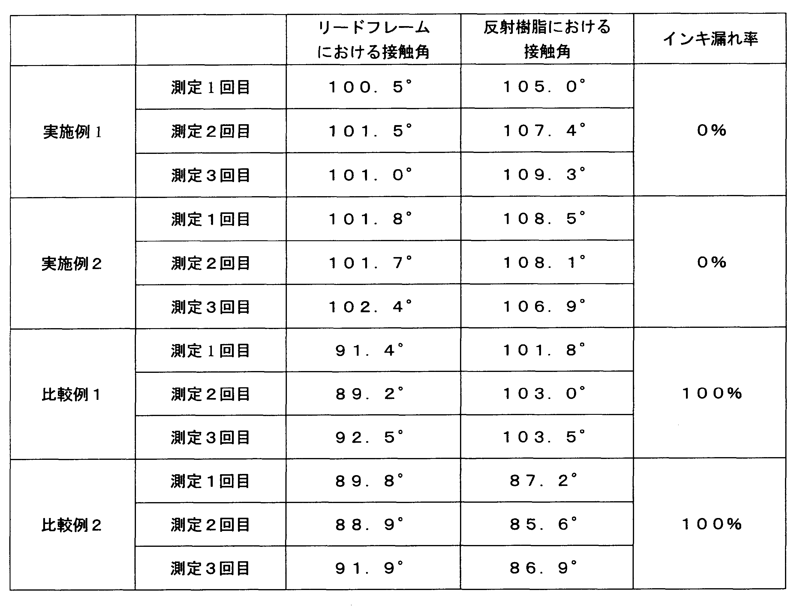
次に、本実施の形態の他の実施例について説明する。
(実施例A)
上記実施例1と略同様に、本実施の形態による樹脂付リードフレーム30(実施例A)を作製した。すなわち、厚さ250μmの銅からなる金属基板31を準備し、この金属基板31に対してエッチングを施すことにより、所定の平面形状を有するリードフレーム本体11を得た(図18(a)-(e))。次に、射出成形法あるいはトランスファ成形法により、リードフレーム本体11に対して熱硬化性樹脂あるいは熱可塑性樹脂からなる反射樹脂23を設けた(図19(a)-(c))。この反射樹脂23には、それぞれLED素子21が収容される256個の凹部23aが形成されていた。次いで、リードフレーム本体11に厚さ3.0μmの銀からなるめっき部12Aを設けた(図19(d))。その後、このようにして得られた樹脂付リードフレーム30を加熱装置39に収容し、窒素雰囲気の下、230℃の温度で2時間加熱した(図19(e))。
上記実施例1と略同様に、本実施の形態による樹脂付リードフレーム30(実施例A)を作製した。すなわち、厚さ250μmの銅からなる金属基板31を準備し、この金属基板31に対してエッチングを施すことにより、所定の平面形状を有するリードフレーム本体11を得た(図18(a)-(e))。次に、射出成形法あるいはトランスファ成形法により、リードフレーム本体11に対して熱硬化性樹脂あるいは熱可塑性樹脂からなる反射樹脂23を設けた(図19(a)-(c))。この反射樹脂23には、それぞれLED素子21が収容される256個の凹部23aが形成されていた。次いで、リードフレーム本体11に厚さ3.0μmの銀からなるめっき部12Aを設けた(図19(d))。その後、このようにして得られた樹脂付リードフレーム30を加熱装置39に収容し、窒素雰囲気の下、230℃の温度で2時間加熱した(図19(e))。
(実施例B)
まずリードフレーム本体11の全体にめっき部12Aを形成し、その後、リードフレーム10のめっき部12A上に反射樹脂23を設けたこと、以外は実施例Aと同様にして、樹脂付リードフレーム30(実施例B)を作製した。その後、このようにして得られた樹脂付リードフレーム30を加熱装置39に収容し、窒素雰囲気の下、230℃の温度で2時間加熱した。
まずリードフレーム本体11の全体にめっき部12Aを形成し、その後、リードフレーム10のめっき部12A上に反射樹脂23を設けたこと、以外は実施例Aと同様にして、樹脂付リードフレーム30(実施例B)を作製した。その後、このようにして得られた樹脂付リードフレーム30を加熱装置39に収容し、窒素雰囲気の下、230℃の温度で2時間加熱した。
(実施例C)
樹脂付リードフレーム30を加熱装置39に収容し、窒素雰囲気の下、150℃の温度で2時間加熱したこと、以外は実施例Aと同様にして、樹脂付リードフレーム(実施例C)を作製した。
樹脂付リードフレーム30を加熱装置39に収容し、窒素雰囲気の下、150℃の温度で2時間加熱したこと、以外は実施例Aと同様にして、樹脂付リードフレーム(実施例C)を作製した。
(比較例a)
樹脂付リードフレームを加熱する工程を設けなかったこと、以外は実施例Bと同様にして、樹脂付リードフレーム(比較例a)を作製した。
樹脂付リードフレームを加熱する工程を設けなかったこと、以外は実施例Bと同様にして、樹脂付リードフレーム(比較例a)を作製した。
(比較例b)
樹脂付リードフレームを加熱する工程を設けなかったこと、以外は実施例Aと同様にして、樹脂付リードフレーム(比較例b)を作製した。
樹脂付リードフレームを加熱する工程を設けなかったこと、以外は実施例Aと同様にして、樹脂付リードフレーム(比較例b)を作製した。
上記6つの樹脂付リードフレーム(実施例A~C、比較例a~b)の各々について、上記と同様に、リードフレーム10および反射樹脂23における純水に対する接触角を測定した。
次に、上記6つの樹脂付リードフレーム(実施例A~C、比較例a~b)のそれぞれについて、上記と同様に、樹脂付リードフレームの上面側からインキを滴下し、一定時間が経過した後、界面41からインキが漏れたか否かを観察した。
以上の結果をまとめて表2に示す。この結果、実施例A~Cについて、インキ漏れ率が0%となり、リードフレーム10と反射樹脂23との界面41における流体(インキ)の侵入を防止することができた。このことから、(i)純水に対するリードフレーム10の接触角が100°以上であり、かつ純水に対する反射樹脂23の接触角が100°以上である場合、又は、(ii)純水に対するリードフレーム10の接触角が95°以上かつ110°以下であり、かつ純水に対する反射樹脂23の接触角が100°以上かつ110°以下である場合に、界面41から流体が侵入することをより効果的に防止することができると考えられる。
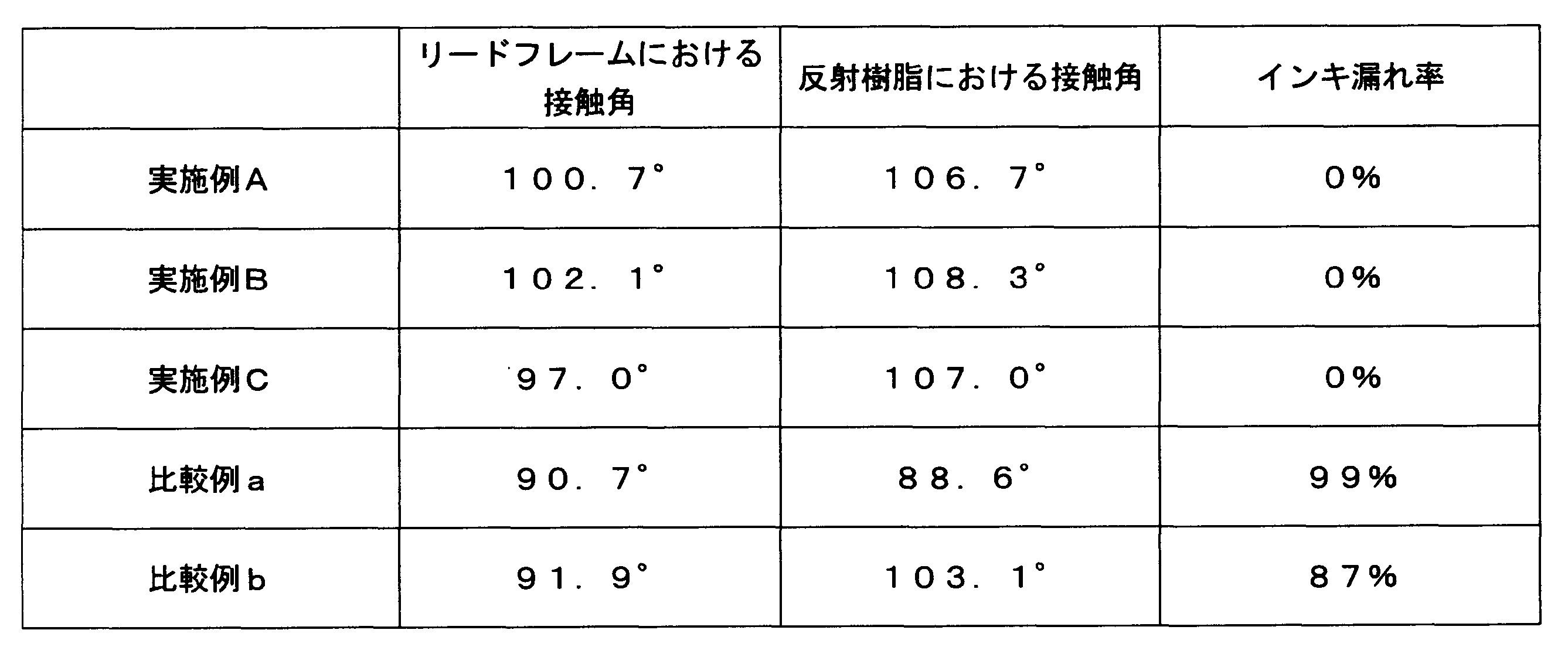
Claims (24)
- 樹脂付リードフレームにおいて、
第1金属部分と、前記第1金属部分から離間して設けられた第2金属部分とを有するリードフレームと、
前記第1金属部分と前記第2金属部分との周囲を取り囲んで設けられ、リードフレームと一体化された反射樹脂とを備え、
少なくとも前記第1金属部分または前記第2金属部分にはアウターリード部が形成され、
前記反射樹脂のうち、前記リードフレームの前記アウターリード部が形成された面側に、複数の突起が形成されていることを特徴とする樹脂付リードフレーム。 - 各突起は、高さが10μm~30μmであり、幅が10μm~100μmであることを特徴とする請求項1記載の樹脂付リードフレーム。
- 前記反射樹脂の裏面の単位面積に占める前記複数の突起の面積の割合は、10%~50%であることを特徴とする請求項1記載の樹脂付リードフレーム。
- 前記複数の突起は、前記第1金属部分の周囲を取り囲む領域又は前記第2金属部分の周囲を取り囲む領域に設けられていることを特徴とする請求項1記載の樹脂付リードフレーム。
- 前記複数の突起は、LEDパッケージの実装面の外形に沿う領域に設けられていることを特徴とする請求項1記載の樹脂付リードフレーム。
- 前記複数の突起は、不規則に配置されていることを特徴とする請求項1記載の樹脂付リードフレーム。
- 少なくとも1つの突起が、前記第1金属部分の裏面の周縁又は前記第2金属部分の裏面の周縁を部分的に覆うことを特徴とする請求項1記載の樹脂付リードフレーム。
- LEDパッケージにおいて、
第1金属部分と、前記第1金属部分から離間して設けられた第2金属部分とを有するリードフレームと、
前記リードフレームの前記第1金属部分に搭載されたLED素子と、
前記LED素子と前記リードフレームの前記第2金属部分とを電気的に接続する導電部と、
前記リードフレームに設けられ、前記LED素子を収容する凹部を有する反射樹脂と、
前記反射樹脂の前記凹部内に充填された封止樹脂とを備え、
前記反射樹脂の裏面に複数の突起が形成されていることを特徴とするLEDパッケージ。 - 樹脂付リードフレームの製造方法において、
第1金属部分と、前記第1金属部分から離間して設けられた前記第2金属部分とを含むリードフレームを準備する工程と、
前記リードフレームに反射樹脂を設ける工程とを備え、
前記リードフレームに反射樹脂を設ける工程において、前記反射樹脂の裏面に複数の突起が形成されることを特徴とする樹脂付リードフレームの製造方法。 - 前記リードフレームに反射樹脂を設ける工程において、前記反射樹脂は焼結金属製の金型を用いて成形され、前記金型は、前記複数の突起に対応する複数の孔を有することを特徴とする請求項9記載の樹脂付リードフレームの製造方法。
- 前記リードフレームに反射樹脂を設けた後、前記リードフレームのうち、前記反射樹脂が設けられていない領域を覆うようにめっき層を設ける工程を更に備えたことを特徴とする請求項9記載の樹脂付リードフレームの製造方法。
- LEDパッケージの製造方法において、
請求項1記載の樹脂付リードフレームを準備する工程と、
前記樹脂付リードフレームの前記第1金属部分にLED素子を搭載する工程と、
前記LED素子と前記樹脂付リードフレームの前記第2金属部分とを導電部により接続する工程と、
前記LED素子および前記導電部を封止樹脂によって封止する工程とを備えたことを特徴とするLEDパッケージの製造方法。 - 樹脂付リードフレームにおいて、
第1金属部分と、前記第1金属部分から離間して設けられた第2金属部分とを有するリードフレームと、
前記リードフレームに設けられた反射樹脂とを備え、
純水に対する前記リードフレームの外面の接触角が100°以上であり、純水に対する前記反射樹脂の外面の接触角が100°以上であることを特徴とする樹脂付リードフレーム。 - 前記リードフレームのうち、前記反射樹脂が設けられていない領域がめっき部によって覆われており、前記リードフレームの接触角が、めっき部の接触角であることを特徴とする請求項13記載の樹脂付リードフレーム。
- 前記反射樹脂と前記リードフレームとの界面に、前記反射樹脂と前記リードフレームとが離間した隙間部が形成され、当該隙間部に前記めっき部が充填されていることを特徴とする請求項14記載の樹脂付リードフレーム。
- 前記リードフレームの外面および前記反射樹脂の外面に、それぞれ撥水性処理膜が形成されていることを特徴とする請求項13記載の樹脂付リードフレーム。
- LEDパッケージにおいて、
第1金属部分と、前記第1金属部分から離間して設けられた第2金属部分とを有するリードフレームと、
前記リードフレームの前記第1金属部分に搭載されたLED素子と、
前記LED素子と前記リードフレームの前記第2金属部分とを電気的に接続する導電部と、
前記リードフレームに設けられ、前記LED素子を収容する凹部を有する反射樹脂と、
前記反射樹脂の前記凹部内に充填された封止樹脂とを備え、
純水に対する前記リードフレームの外面の接触角が100°以上であり、純水に対する前記反射樹脂の外面の接触角が100°以上であることを特徴とするLEDパッケージ。 - 樹脂付リードフレームの製造方法において、
第1金属部分と、前記第1金属部分から離間して設けられた前記第2金属部分とを含むリードフレームを準備する工程と、
前記リードフレームに反射樹脂を設ける工程とを備え、
純水に対する前記リードフレームの外面の接触角が100°以上であり、純水に対する前記反射樹脂の外面の接触角が100°以上であることを特徴とする樹脂付リードフレームの製造方法。 - 前記リードフレームに反射樹脂を設ける工程の後、前記リードフレームおよび前記反射樹脂の撥水性を高める工程が設けられていることを特徴とする請求項18記載の樹脂付リードフレームの製造方法。
- 前記リードフレームおよび前記反射樹脂の撥水性を高める工程は、前記リードフレームおよび前記反射樹脂を加熱する工程であることを特徴とする請求項19記載の樹脂付リードフレームの製造方法。
- 前記リードフレームおよび前記反射樹脂は、100℃~250℃の温度で加熱されることを特徴とする請求項20記載の樹脂付リードフレームの製造方法。
- 前記リードフレームおよび前記反射樹脂の撥水性を高める工程は、前記リードフレームの外面および前記反射樹脂の外面に撥水性処理膜を形成する工程であることを特徴とする請求項19記載の樹脂付リードフレームの製造方法。
- LEDパッケージの製造方法において、
請求項13記載の樹脂付リードフレームを準備する工程と、
前記樹脂付リードフレームの前記第1金属部分にLED素子を搭載する工程と、
前記LED素子と前記樹脂付リードフレームの前記第2金属部分とを導電部により接続する工程と、
前記LED素子および前記導電部を封止樹脂によって封止する工程とを備えたことを特徴とするLEDパッケージの製造方法。 - 樹脂付リードフレームにおいて、
第1金属部分と、前記第1金属部分から離間して設けられた第2金属部分とを有するリードフレームと、
前記リードフレームに設けられた反射樹脂とを備え、
純水に対する前記リードフレームの外面の接触角が95°以上かつ110°以下であり、純水に対する前記反射樹脂の外面の接触角が100°以上かつ110°以下であることを特徴とする樹脂付リードフレーム。
Priority Applications (1)
| Application Number | Priority Date | Filing Date | Title |
|---|---|---|---|
| PCT/JP2015/078093 WO2017056321A1 (ja) | 2015-10-02 | 2015-10-02 | 樹脂付リードフレームおよびその製造方法、ならびにledパッケージおよびその製造方法 |
Applications Claiming Priority (1)
| Application Number | Priority Date | Filing Date | Title |
|---|---|---|---|
| PCT/JP2015/078093 WO2017056321A1 (ja) | 2015-10-02 | 2015-10-02 | 樹脂付リードフレームおよびその製造方法、ならびにledパッケージおよびその製造方法 |
Publications (1)
| Publication Number | Publication Date |
|---|---|
| WO2017056321A1 true WO2017056321A1 (ja) | 2017-04-06 |
Family
ID=58423045
Family Applications (1)
| Application Number | Title | Priority Date | Filing Date |
|---|---|---|---|
| PCT/JP2015/078093 Ceased WO2017056321A1 (ja) | 2015-10-02 | 2015-10-02 | 樹脂付リードフレームおよびその製造方法、ならびにledパッケージおよびその製造方法 |
Country Status (1)
| Country | Link |
|---|---|
| WO (1) | WO2017056321A1 (ja) |
Cited By (3)
| Publication number | Priority date | Publication date | Assignee | Title |
|---|---|---|---|---|
| WO2019219177A1 (en) * | 2018-05-15 | 2019-11-21 | Osram Opto Semiconductors Gmbh | Carrier for an optoelectronic device, method for producing a carrier for an optoelectronic device |
| US20220029066A1 (en) * | 2018-09-12 | 2022-01-27 | Nichia Corporation | Method of producing light source device comprising joining a wiring portion of a light emitting device and a support substrate by a solder member |
| DE102023104437A1 (de) * | 2023-02-23 | 2024-08-29 | Ams-Osram International Gmbh | Elektronisches Bauelement und Verfahren zum Montieren eines elektronischen Bauelements |
Citations (2)
| Publication number | Priority date | Publication date | Assignee | Title |
|---|---|---|---|---|
| US20110291152A1 (en) * | 2010-05-31 | 2011-12-01 | Hon Hai Precision Industry Co., Ltd. | Led lead frame with water-repellent layer |
| WO2012102266A1 (ja) * | 2011-01-27 | 2012-08-02 | 大日本印刷株式会社 | 樹脂付リードフレームおよびその製造方法、ならびにリードフレーム |
-
2015
- 2015-10-02 WO PCT/JP2015/078093 patent/WO2017056321A1/ja not_active Ceased
Patent Citations (2)
| Publication number | Priority date | Publication date | Assignee | Title |
|---|---|---|---|---|
| US20110291152A1 (en) * | 2010-05-31 | 2011-12-01 | Hon Hai Precision Industry Co., Ltd. | Led lead frame with water-repellent layer |
| WO2012102266A1 (ja) * | 2011-01-27 | 2012-08-02 | 大日本印刷株式会社 | 樹脂付リードフレームおよびその製造方法、ならびにリードフレーム |
Cited By (4)
| Publication number | Priority date | Publication date | Assignee | Title |
|---|---|---|---|---|
| WO2019219177A1 (en) * | 2018-05-15 | 2019-11-21 | Osram Opto Semiconductors Gmbh | Carrier for an optoelectronic device, method for producing a carrier for an optoelectronic device |
| US20220029066A1 (en) * | 2018-09-12 | 2022-01-27 | Nichia Corporation | Method of producing light source device comprising joining a wiring portion of a light emitting device and a support substrate by a solder member |
| US11799062B2 (en) * | 2018-09-12 | 2023-10-24 | Nichia Corporation | Method of producing light source device comprising joining a wiring portion of a light emitting device and a support substrate by a solder member |
| DE102023104437A1 (de) * | 2023-02-23 | 2024-08-29 | Ams-Osram International Gmbh | Elektronisches Bauelement und Verfahren zum Montieren eines elektronischen Bauelements |
Similar Documents
| Publication | Publication Date | Title |
|---|---|---|
| US10263166B2 (en) | Light emitting device | |
| CN102804428B (zh) | Led用引线框或基板、半导体装置和led用引线框或基板的制造方法 | |
| US9461207B2 (en) | Light emitting device, and package array for light emitting device | |
| US20200176649A1 (en) | Method of manufacturing light emitting device | |
| JP2022168010A (ja) | 光半導体装置用金属材料、及びその製造方法、及びそれを用いた光半導体装置 | |
| JP2018032655A (ja) | 発光装置及びその製造方法 | |
| JP5970835B2 (ja) | リードフレーム部材、樹脂付リードフレーム部材および半導体装置 | |
| JP2012174966A (ja) | 半導体発光装置用リードフレーム及びその製造方法 | |
| US12559648B2 (en) | Method of manufacturing metal structure for optical semiconductor device, package, and solution containing polyallylamine polymer | |
| JP5871174B2 (ja) | Led用リードフレームまたは基板、半導体装置、およびled用リードフレームまたは基板の製造方法 | |
| WO2017056321A1 (ja) | 樹脂付リードフレームおよびその製造方法、ならびにledパッケージおよびその製造方法 | |
| JP2018056457A (ja) | 発光装置、発光装置用パッケージ及び発光装置の製造方法 | |
| JP6548066B2 (ja) | Led素子搭載用リードフレーム、led素子搭載用樹脂付きリードフレーム及び半導体装置 | |
| JP2016001702A (ja) | 樹脂付リードフレームおよびその製造方法、ならびにledパッケージおよびその製造方法 | |
| JP2011228687A (ja) | Led用リードフレームまたは基板、半導体装置、およびled用リードフレームまたは基板の製造方法 | |
| JP2015201608A (ja) | 樹脂付リードフレームおよびその製造方法、ならびにledパッケージおよびその製造方法 | |
| JP2013077727A (ja) | Led発光素子用リードフレーム基板 | |
| JP5941614B2 (ja) | 半導体装置およびその製造方法 | |
| JP2016119466A (ja) | 発光装置 | |
| JP6701711B2 (ja) | 発光装置 | |
| JP7116308B2 (ja) | 光半導体装置用金属材料、及びその製造方法、及びそれを用いた光半導体装置 | |
| JP7148793B2 (ja) | 光半導体装置用金属材料、及びその製造方法、及びそれを用いた光半導体装置 | |
| JP2015188081A (ja) | 樹脂付リードフレームおよびその製造方法、ならびにledパッケージおよびその製造方法 | |
| KR101199216B1 (ko) | 발광 다이오드 패키지 | |
| TWI464928B (zh) | 發光二極體基板結構、發光二極體單元及其光源模組 |
Legal Events
| Date | Code | Title | Description |
|---|---|---|---|
| 121 | Ep: the epo has been informed by wipo that ep was designated in this application |
Ref document number: 15905474 Country of ref document: EP Kind code of ref document: A1 |
|
| NENP | Non-entry into the national phase |
Ref country code: DE |
|
| 122 | Ep: pct application non-entry in european phase |
Ref document number: 15905474 Country of ref document: EP Kind code of ref document: A1 |
|
| NENP | Non-entry into the national phase |
Ref country code: JP |