WO2017047152A1 - Oxide sintered body, method for producing same, sputtering target and method for manufacturing semiconductor device - Google Patents
Oxide sintered body, method for producing same, sputtering target and method for manufacturing semiconductor device Download PDFInfo
- Publication number
- WO2017047152A1 WO2017047152A1 PCT/JP2016/063646 JP2016063646W WO2017047152A1 WO 2017047152 A1 WO2017047152 A1 WO 2017047152A1 JP 2016063646 W JP2016063646 W JP 2016063646W WO 2017047152 A1 WO2017047152 A1 WO 2017047152A1
- Authority
- WO
- WIPO (PCT)
- Prior art keywords
- oxide
- sintered body
- crystal phase
- oxide sintered
- powder
- Prior art date
Links
- 239000004065 semiconductor Substances 0.000 title claims description 260
- 238000004519 manufacturing process Methods 0.000 title claims description 81
- 238000004544 sputter deposition Methods 0.000 title claims description 56
- 238000005477 sputtering target Methods 0.000 title description 23
- 239000013078 crystal Substances 0.000 claims abstract description 279
- 239000011701 zinc Substances 0.000 claims abstract description 154
- 229910052738 indium Inorganic materials 0.000 claims abstract description 92
- 229910052725 zinc Inorganic materials 0.000 claims abstract description 85
- 229910052721 tungsten Inorganic materials 0.000 claims abstract description 84
- APFVFJFRJDLVQX-UHFFFAOYSA-N indium atom Chemical compound [In] APFVFJFRJDLVQX-UHFFFAOYSA-N 0.000 claims abstract description 41
- 239000002245 particle Substances 0.000 claims abstract description 36
- WFKWXMTUELFFGS-UHFFFAOYSA-N tungsten Chemical compound [W] WFKWXMTUELFFGS-UHFFFAOYSA-N 0.000 claims abstract description 31
- 239000010937 tungsten Substances 0.000 claims abstract description 31
- HCHKCACWOHOZIP-UHFFFAOYSA-N Zinc Chemical compound [Zn] HCHKCACWOHOZIP-UHFFFAOYSA-N 0.000 claims abstract description 30
- 239000000843 powder Substances 0.000 claims description 200
- 239000000203 mixture Substances 0.000 claims description 86
- 238000000034 method Methods 0.000 claims description 85
- XLOMVQKBTHCTTD-UHFFFAOYSA-N Zinc monoxide Chemical compound [Zn]=O XLOMVQKBTHCTTD-UHFFFAOYSA-N 0.000 claims description 47
- QGLKJKCYBOYXKC-UHFFFAOYSA-N nonaoxidotritungsten Chemical compound O=[W]1(=O)O[W](=O)(=O)O[W](=O)(=O)O1 QGLKJKCYBOYXKC-UHFFFAOYSA-N 0.000 claims description 43
- 229910001930 tungsten oxide Inorganic materials 0.000 claims description 43
- 238000002441 X-ray diffraction Methods 0.000 claims description 33
- 239000002994 raw material Substances 0.000 claims description 33
- 238000005245 sintering Methods 0.000 claims description 33
- 239000012298 atmosphere Substances 0.000 claims description 32
- 229910052760 oxygen Inorganic materials 0.000 claims description 31
- QVGXLLKOCUKJST-UHFFFAOYSA-N atomic oxygen Chemical compound [O] QVGXLLKOCUKJST-UHFFFAOYSA-N 0.000 claims description 28
- 239000001301 oxygen Substances 0.000 claims description 28
- 229910003437 indium oxide Inorganic materials 0.000 claims description 19
- PJXISJQVUVHSOJ-UHFFFAOYSA-N indium(iii) oxide Chemical compound [O-2].[O-2].[O-2].[In+3].[In+3] PJXISJQVUVHSOJ-UHFFFAOYSA-N 0.000 claims description 19
- 238000000465 moulding Methods 0.000 claims description 8
- 239000010408 film Substances 0.000 description 247
- 238000010438 heat treatment Methods 0.000 description 57
- 230000005669 field effect Effects 0.000 description 42
- 239000000758 substrate Substances 0.000 description 41
- 230000015572 biosynthetic process Effects 0.000 description 40
- 230000001965 increasing effect Effects 0.000 description 36
- 238000005259 measurement Methods 0.000 description 29
- -1 indium tungstate compound Chemical class 0.000 description 28
- 238000002161 passivation Methods 0.000 description 24
- 239000007789 gas Substances 0.000 description 21
- 230000000052 comparative effect Effects 0.000 description 19
- 229910052751 metal Inorganic materials 0.000 description 17
- 239000011787 zinc oxide Substances 0.000 description 16
- 238000002156 mixing Methods 0.000 description 15
- 238000001354 calcination Methods 0.000 description 14
- 239000002184 metal Substances 0.000 description 13
- IJGRMHOSHXDMSA-UHFFFAOYSA-N Atomic nitrogen Chemical compound N#N IJGRMHOSHXDMSA-UHFFFAOYSA-N 0.000 description 12
- 239000010949 copper Substances 0.000 description 12
- LIVNPJMFVYWSIS-UHFFFAOYSA-N silicon monoxide Chemical compound [Si-]#[O+] LIVNPJMFVYWSIS-UHFFFAOYSA-N 0.000 description 12
- 238000005001 rutherford backscattering spectroscopy Methods 0.000 description 10
- XLYOFNOQVPJJNP-UHFFFAOYSA-N water Substances O XLYOFNOQVPJJNP-UHFFFAOYSA-N 0.000 description 10
- VYPSYNLAJGMNEJ-UHFFFAOYSA-N Silicium dioxide Chemical compound O=[Si]=O VYPSYNLAJGMNEJ-UHFFFAOYSA-N 0.000 description 9
- 239000000463 material Substances 0.000 description 9
- 239000012299 nitrogen atmosphere Substances 0.000 description 9
- 229910052984 zinc sulfide Inorganic materials 0.000 description 9
- 230000005540 biological transmission Effects 0.000 description 8
- 230000002950 deficient Effects 0.000 description 8
- 238000005530 etching Methods 0.000 description 8
- 238000005211 surface analysis Methods 0.000 description 8
- RYGMFSIKBFXOCR-UHFFFAOYSA-N Copper Chemical compound [Cu] RYGMFSIKBFXOCR-UHFFFAOYSA-N 0.000 description 7
- XUIMIQQOPSSXEZ-UHFFFAOYSA-N Silicon Chemical compound [Si] XUIMIQQOPSSXEZ-UHFFFAOYSA-N 0.000 description 7
- 229910052782 aluminium Inorganic materials 0.000 description 7
- XAGFODPZIPBFFR-UHFFFAOYSA-N aluminium Chemical compound [Al] XAGFODPZIPBFFR-UHFFFAOYSA-N 0.000 description 7
- 239000002131 composite material Substances 0.000 description 7
- 238000012790 confirmation Methods 0.000 description 7
- 229910052802 copper Inorganic materials 0.000 description 7
- 238000005336 cracking Methods 0.000 description 7
- 238000005268 plasma chemical vapour deposition Methods 0.000 description 7
- 229910052710 silicon Inorganic materials 0.000 description 7
- 239000010703 silicon Substances 0.000 description 7
- 229910052814 silicon oxide Inorganic materials 0.000 description 7
- 238000009413 insulation Methods 0.000 description 6
- TWNQGVIAIRXVLR-UHFFFAOYSA-N oxo(oxoalumanyloxy)alumane Chemical compound O=[Al]O[Al]=O TWNQGVIAIRXVLR-UHFFFAOYSA-N 0.000 description 6
- 238000010298 pulverizing process Methods 0.000 description 6
- 239000006104 solid solution Substances 0.000 description 6
- 239000010409 thin film Substances 0.000 description 6
- 229910021417 amorphous silicon Inorganic materials 0.000 description 5
- XKRFYHLGVUSROY-UHFFFAOYSA-N argon Substances [Ar] XKRFYHLGVUSROY-UHFFFAOYSA-N 0.000 description 5
- 238000001816 cooling Methods 0.000 description 5
- 238000000151 deposition Methods 0.000 description 5
- 229910001882 dioxygen Inorganic materials 0.000 description 5
- 229910052757 nitrogen Inorganic materials 0.000 description 5
- 238000002360 preparation method Methods 0.000 description 5
- LFQSCWFLJHTTHZ-UHFFFAOYSA-N Ethanol Chemical compound CCO LFQSCWFLJHTTHZ-UHFFFAOYSA-N 0.000 description 4
- 238000004458 analytical method Methods 0.000 description 4
- 238000001035 drying Methods 0.000 description 4
- 238000011156 evaluation Methods 0.000 description 4
- 238000009616 inductively coupled plasma Methods 0.000 description 4
- 238000001755 magnetron sputter deposition Methods 0.000 description 4
- 239000002159 nanocrystal Substances 0.000 description 4
- MUBZPKHOEPUJKR-UHFFFAOYSA-N Oxalic acid Chemical compound OC(=O)C(O)=O MUBZPKHOEPUJKR-UHFFFAOYSA-N 0.000 description 3
- 229910052581 Si3N4 Inorganic materials 0.000 description 3
- 229910052786 argon Inorganic materials 0.000 description 3
- 238000011088 calibration curve Methods 0.000 description 3
- 238000005229 chemical vapour deposition Methods 0.000 description 3
- 230000008021 deposition Effects 0.000 description 3
- 238000002003 electron diffraction Methods 0.000 description 3
- 125000005843 halogen group Chemical group 0.000 description 3
- 150000002500 ions Chemical group 0.000 description 3
- 238000004949 mass spectrometry Methods 0.000 description 3
- 229920002120 photoresistant polymer Polymers 0.000 description 3
- 230000000704 physical effect Effects 0.000 description 3
- HQVNEWCFYHHQES-UHFFFAOYSA-N silicon nitride Chemical compound N12[Si]34N5[Si]62N3[Si]51N64 HQVNEWCFYHHQES-UHFFFAOYSA-N 0.000 description 3
- 239000000126 substance Substances 0.000 description 3
- JBQYATWDVHIOAR-UHFFFAOYSA-N tellanylidenegermanium Chemical compound [Te]=[Ge] JBQYATWDVHIOAR-UHFFFAOYSA-N 0.000 description 3
- 238000001771 vacuum deposition Methods 0.000 description 3
- OLBVUFHMDRJKTK-UHFFFAOYSA-N [N].[O] Chemical compound [N].[O] OLBVUFHMDRJKTK-UHFFFAOYSA-N 0.000 description 2
- 239000007864 aqueous solution Substances 0.000 description 2
- 125000004429 atom Chemical group 0.000 description 2
- 239000011324 bead Substances 0.000 description 2
- 229910001873 dinitrogen Inorganic materials 0.000 description 2
- 239000002612 dispersion medium Substances 0.000 description 2
- 238000010894 electron beam technology Methods 0.000 description 2
- 230000002708 enhancing effect Effects 0.000 description 2
- 239000011521 glass Substances 0.000 description 2
- 230000003647 oxidation Effects 0.000 description 2
- 238000007254 oxidation reaction Methods 0.000 description 2
- 238000012545 processing Methods 0.000 description 2
- VSZWPYCFIRKVQL-UHFFFAOYSA-N selanylidenegallium;selenium Chemical compound [Se].[Se]=[Ga].[Se]=[Ga] VSZWPYCFIRKVQL-UHFFFAOYSA-N 0.000 description 2
- 239000007921 spray Substances 0.000 description 2
- 238000012360 testing method Methods 0.000 description 2
- PBYZMCDFOULPGH-UHFFFAOYSA-N tungstate Chemical compound [O-][W]([O-])(=O)=O PBYZMCDFOULPGH-UHFFFAOYSA-N 0.000 description 2
- 230000000007 visual effect Effects 0.000 description 2
- 238000007088 Archimedes method Methods 0.000 description 1
- MYMOFIZGZYHOMD-UHFFFAOYSA-N Dioxygen Chemical compound O=O MYMOFIZGZYHOMD-UHFFFAOYSA-N 0.000 description 1
- GYHNNYVSQQEPJS-UHFFFAOYSA-N Gallium Chemical compound [Ga] GYHNNYVSQQEPJS-UHFFFAOYSA-N 0.000 description 1
- QCWXUUIWCKQGHC-UHFFFAOYSA-N Zirconium Chemical compound [Zr] QCWXUUIWCKQGHC-UHFFFAOYSA-N 0.000 description 1
- 230000001133 acceleration Effects 0.000 description 1
- 239000003513 alkali Substances 0.000 description 1
- PNEYBMLMFCGWSK-UHFFFAOYSA-N aluminium oxide Inorganic materials [O-2].[O-2].[O-2].[Al+3].[Al+3] PNEYBMLMFCGWSK-UHFFFAOYSA-N 0.000 description 1
- 239000002585 base Substances 0.000 description 1
- 238000004364 calculation method Methods 0.000 description 1
- 239000000969 carrier Substances 0.000 description 1
- 238000005266 casting Methods 0.000 description 1
- 239000000470 constituent Substances 0.000 description 1
- 238000005520 cutting process Methods 0.000 description 1
- 230000003247 decreasing effect Effects 0.000 description 1
- 238000001312 dry etching Methods 0.000 description 1
- 230000000694 effects Effects 0.000 description 1
- 238000005401 electroluminescence Methods 0.000 description 1
- 238000002474 experimental method Methods 0.000 description 1
- 229910052733 gallium Inorganic materials 0.000 description 1
- 238000000227 grinding Methods 0.000 description 1
- 239000012212 insulator Substances 0.000 description 1
- 239000004973 liquid crystal related substance Substances 0.000 description 1
- 238000000691 measurement method Methods 0.000 description 1
- 238000002844 melting Methods 0.000 description 1
- 230000008018 melting Effects 0.000 description 1
- 239000011812 mixed powder Substances 0.000 description 1
- 238000012986 modification Methods 0.000 description 1
- 230000004048 modification Effects 0.000 description 1
- 235000006408 oxalic acid Nutrition 0.000 description 1
- 238000001020 plasma etching Methods 0.000 description 1
- 238000000634 powder X-ray diffraction Methods 0.000 description 1
- 238000003825 pressing Methods 0.000 description 1
- 229910001404 rare earth metal oxide Inorganic materials 0.000 description 1
- 239000002689 soil Substances 0.000 description 1
- 239000007787 solid Substances 0.000 description 1
- 238000001694 spray drying Methods 0.000 description 1
- 238000009864 tensile test Methods 0.000 description 1
- 238000001039 wet etching Methods 0.000 description 1
- 229910052726 zirconium Inorganic materials 0.000 description 1
Images


Classifications
-
- C—CHEMISTRY; METALLURGY
- C04—CEMENTS; CONCRETE; ARTIFICIAL STONE; CERAMICS; REFRACTORIES
- C04B—LIME, MAGNESIA; SLAG; CEMENTS; COMPOSITIONS THEREOF, e.g. MORTARS, CONCRETE OR LIKE BUILDING MATERIALS; ARTIFICIAL STONE; CERAMICS; REFRACTORIES; TREATMENT OF NATURAL STONE
- C04B35/00—Shaped ceramic products characterised by their composition; Ceramics compositions; Processing powders of inorganic compounds preparatory to the manufacturing of ceramic products
- C04B35/01—Shaped ceramic products characterised by their composition; Ceramics compositions; Processing powders of inorganic compounds preparatory to the manufacturing of ceramic products based on oxide ceramics
- C04B35/495—Shaped ceramic products characterised by their composition; Ceramics compositions; Processing powders of inorganic compounds preparatory to the manufacturing of ceramic products based on oxide ceramics based on vanadium, niobium, tantalum, molybdenum or tungsten oxides or solid solutions thereof with other oxides, e.g. vanadates, niobates, tantalates, molybdates or tungstates
-
- C—CHEMISTRY; METALLURGY
- C23—COATING METALLIC MATERIAL; COATING MATERIAL WITH METALLIC MATERIAL; CHEMICAL SURFACE TREATMENT; DIFFUSION TREATMENT OF METALLIC MATERIAL; COATING BY VACUUM EVAPORATION, BY SPUTTERING, BY ION IMPLANTATION OR BY CHEMICAL VAPOUR DEPOSITION, IN GENERAL; INHIBITING CORROSION OF METALLIC MATERIAL OR INCRUSTATION IN GENERAL
- C23C—COATING METALLIC MATERIAL; COATING MATERIAL WITH METALLIC MATERIAL; SURFACE TREATMENT OF METALLIC MATERIAL BY DIFFUSION INTO THE SURFACE, BY CHEMICAL CONVERSION OR SUBSTITUTION; COATING BY VACUUM EVAPORATION, BY SPUTTERING, BY ION IMPLANTATION OR BY CHEMICAL VAPOUR DEPOSITION, IN GENERAL
- C23C14/00—Coating by vacuum evaporation, by sputtering or by ion implantation of the coating forming material
- C23C14/22—Coating by vacuum evaporation, by sputtering or by ion implantation of the coating forming material characterised by the process of coating
- C23C14/34—Sputtering
- C23C14/3407—Cathode assembly for sputtering apparatus, e.g. Target
- C23C14/3414—Metallurgical or chemical aspects of target preparation, e.g. casting, powder metallurgy
-
- C—CHEMISTRY; METALLURGY
- C04—CEMENTS; CONCRETE; ARTIFICIAL STONE; CERAMICS; REFRACTORIES
- C04B—LIME, MAGNESIA; SLAG; CEMENTS; COMPOSITIONS THEREOF, e.g. MORTARS, CONCRETE OR LIKE BUILDING MATERIALS; ARTIFICIAL STONE; CERAMICS; REFRACTORIES; TREATMENT OF NATURAL STONE
- C04B35/00—Shaped ceramic products characterised by their composition; Ceramics compositions; Processing powders of inorganic compounds preparatory to the manufacturing of ceramic products
- C04B35/01—Shaped ceramic products characterised by their composition; Ceramics compositions; Processing powders of inorganic compounds preparatory to the manufacturing of ceramic products based on oxide ceramics
- C04B35/453—Shaped ceramic products characterised by their composition; Ceramics compositions; Processing powders of inorganic compounds preparatory to the manufacturing of ceramic products based on oxide ceramics based on zinc, tin, or bismuth oxides or solid solutions thereof with other oxides, e.g. zincates, stannates or bismuthates
-
- C—CHEMISTRY; METALLURGY
- C04—CEMENTS; CONCRETE; ARTIFICIAL STONE; CERAMICS; REFRACTORIES
- C04B—LIME, MAGNESIA; SLAG; CEMENTS; COMPOSITIONS THEREOF, e.g. MORTARS, CONCRETE OR LIKE BUILDING MATERIALS; ARTIFICIAL STONE; CERAMICS; REFRACTORIES; TREATMENT OF NATURAL STONE
- C04B35/00—Shaped ceramic products characterised by their composition; Ceramics compositions; Processing powders of inorganic compounds preparatory to the manufacturing of ceramic products
- C04B35/622—Forming processes; Processing powders of inorganic compounds preparatory to the manufacturing of ceramic products
- C04B35/626—Preparing or treating the powders individually or as batches ; preparing or treating macroscopic reinforcing agents for ceramic products, e.g. fibres; mechanical aspects section B
- C04B35/62605—Treating the starting powders individually or as mixtures
- C04B35/62645—Thermal treatment of powders or mixtures thereof other than sintering
-
- C—CHEMISTRY; METALLURGY
- C04—CEMENTS; CONCRETE; ARTIFICIAL STONE; CERAMICS; REFRACTORIES
- C04B—LIME, MAGNESIA; SLAG; CEMENTS; COMPOSITIONS THEREOF, e.g. MORTARS, CONCRETE OR LIKE BUILDING MATERIALS; ARTIFICIAL STONE; CERAMICS; REFRACTORIES; TREATMENT OF NATURAL STONE
- C04B35/00—Shaped ceramic products characterised by their composition; Ceramics compositions; Processing powders of inorganic compounds preparatory to the manufacturing of ceramic products
- C04B35/622—Forming processes; Processing powders of inorganic compounds preparatory to the manufacturing of ceramic products
- C04B35/64—Burning or sintering processes
-
- C—CHEMISTRY; METALLURGY
- C23—COATING METALLIC MATERIAL; COATING MATERIAL WITH METALLIC MATERIAL; CHEMICAL SURFACE TREATMENT; DIFFUSION TREATMENT OF METALLIC MATERIAL; COATING BY VACUUM EVAPORATION, BY SPUTTERING, BY ION IMPLANTATION OR BY CHEMICAL VAPOUR DEPOSITION, IN GENERAL; INHIBITING CORROSION OF METALLIC MATERIAL OR INCRUSTATION IN GENERAL
- C23C—COATING METALLIC MATERIAL; COATING MATERIAL WITH METALLIC MATERIAL; SURFACE TREATMENT OF METALLIC MATERIAL BY DIFFUSION INTO THE SURFACE, BY CHEMICAL CONVERSION OR SUBSTITUTION; COATING BY VACUUM EVAPORATION, BY SPUTTERING, BY ION IMPLANTATION OR BY CHEMICAL VAPOUR DEPOSITION, IN GENERAL
- C23C14/00—Coating by vacuum evaporation, by sputtering or by ion implantation of the coating forming material
- C23C14/06—Coating by vacuum evaporation, by sputtering or by ion implantation of the coating forming material characterised by the coating material
- C23C14/08—Oxides
- C23C14/083—Oxides of refractory metals or yttrium
-
- C—CHEMISTRY; METALLURGY
- C23—COATING METALLIC MATERIAL; COATING MATERIAL WITH METALLIC MATERIAL; CHEMICAL SURFACE TREATMENT; DIFFUSION TREATMENT OF METALLIC MATERIAL; COATING BY VACUUM EVAPORATION, BY SPUTTERING, BY ION IMPLANTATION OR BY CHEMICAL VAPOUR DEPOSITION, IN GENERAL; INHIBITING CORROSION OF METALLIC MATERIAL OR INCRUSTATION IN GENERAL
- C23C—COATING METALLIC MATERIAL; COATING MATERIAL WITH METALLIC MATERIAL; SURFACE TREATMENT OF METALLIC MATERIAL BY DIFFUSION INTO THE SURFACE, BY CHEMICAL CONVERSION OR SUBSTITUTION; COATING BY VACUUM EVAPORATION, BY SPUTTERING, BY ION IMPLANTATION OR BY CHEMICAL VAPOUR DEPOSITION, IN GENERAL
- C23C14/00—Coating by vacuum evaporation, by sputtering or by ion implantation of the coating forming material
- C23C14/06—Coating by vacuum evaporation, by sputtering or by ion implantation of the coating forming material characterised by the coating material
- C23C14/08—Oxides
- C23C14/086—Oxides of zinc, germanium, cadmium, indium, tin, thallium or bismuth
-
- C—CHEMISTRY; METALLURGY
- C23—COATING METALLIC MATERIAL; COATING MATERIAL WITH METALLIC MATERIAL; CHEMICAL SURFACE TREATMENT; DIFFUSION TREATMENT OF METALLIC MATERIAL; COATING BY VACUUM EVAPORATION, BY SPUTTERING, BY ION IMPLANTATION OR BY CHEMICAL VAPOUR DEPOSITION, IN GENERAL; INHIBITING CORROSION OF METALLIC MATERIAL OR INCRUSTATION IN GENERAL
- C23C—COATING METALLIC MATERIAL; COATING MATERIAL WITH METALLIC MATERIAL; SURFACE TREATMENT OF METALLIC MATERIAL BY DIFFUSION INTO THE SURFACE, BY CHEMICAL CONVERSION OR SUBSTITUTION; COATING BY VACUUM EVAPORATION, BY SPUTTERING, BY ION IMPLANTATION OR BY CHEMICAL VAPOUR DEPOSITION, IN GENERAL
- C23C14/00—Coating by vacuum evaporation, by sputtering or by ion implantation of the coating forming material
- C23C14/22—Coating by vacuum evaporation, by sputtering or by ion implantation of the coating forming material characterised by the process of coating
- C23C14/34—Sputtering
-
- H—ELECTRICITY
- H01—ELECTRIC ELEMENTS
- H01J—ELECTRIC DISCHARGE TUBES OR DISCHARGE LAMPS
- H01J37/00—Discharge tubes with provision for introducing objects or material to be exposed to the discharge, e.g. for the purpose of examination or processing thereof
- H01J37/32—Gas-filled discharge tubes
- H01J37/34—Gas-filled discharge tubes operating with cathodic sputtering
- H01J37/3411—Constructional aspects of the reactor
- H01J37/3414—Targets
- H01J37/3426—Material
-
- H—ELECTRICITY
- H01—ELECTRIC ELEMENTS
- H01L—SEMICONDUCTOR DEVICES NOT COVERED BY CLASS H10
- H01L21/00—Processes or apparatus adapted for the manufacture or treatment of semiconductor or solid state devices or of parts thereof
- H01L21/02—Manufacture or treatment of semiconductor devices or of parts thereof
- H01L21/02104—Forming layers
- H01L21/02365—Forming inorganic semiconducting materials on a substrate
- H01L21/02518—Deposited layers
- H01L21/02521—Materials
- H01L21/02551—Group 12/16 materials
- H01L21/02554—Oxides
-
- H—ELECTRICITY
- H01—ELECTRIC ELEMENTS
- H01L—SEMICONDUCTOR DEVICES NOT COVERED BY CLASS H10
- H01L21/00—Processes or apparatus adapted for the manufacture or treatment of semiconductor or solid state devices or of parts thereof
- H01L21/02—Manufacture or treatment of semiconductor devices or of parts thereof
- H01L21/02104—Forming layers
- H01L21/02365—Forming inorganic semiconducting materials on a substrate
- H01L21/02518—Deposited layers
- H01L21/02521—Materials
- H01L21/02565—Oxide semiconducting materials not being Group 12/16 materials, e.g. ternary compounds
-
- H—ELECTRICITY
- H01—ELECTRIC ELEMENTS
- H01L—SEMICONDUCTOR DEVICES NOT COVERED BY CLASS H10
- H01L21/00—Processes or apparatus adapted for the manufacture or treatment of semiconductor or solid state devices or of parts thereof
- H01L21/02—Manufacture or treatment of semiconductor devices or of parts thereof
- H01L21/02104—Forming layers
- H01L21/02365—Forming inorganic semiconducting materials on a substrate
- H01L21/02518—Deposited layers
- H01L21/0257—Doping during depositing
-
- H—ELECTRICITY
- H01—ELECTRIC ELEMENTS
- H01L—SEMICONDUCTOR DEVICES NOT COVERED BY CLASS H10
- H01L21/00—Processes or apparatus adapted for the manufacture or treatment of semiconductor or solid state devices or of parts thereof
- H01L21/02—Manufacture or treatment of semiconductor devices or of parts thereof
- H01L21/02104—Forming layers
- H01L21/02365—Forming inorganic semiconducting materials on a substrate
- H01L21/02518—Deposited layers
- H01L21/02587—Structure
- H01L21/0259—Microstructure
- H01L21/02592—Microstructure amorphous
-
- H—ELECTRICITY
- H01—ELECTRIC ELEMENTS
- H01L—SEMICONDUCTOR DEVICES NOT COVERED BY CLASS H10
- H01L21/00—Processes or apparatus adapted for the manufacture or treatment of semiconductor or solid state devices or of parts thereof
- H01L21/02—Manufacture or treatment of semiconductor devices or of parts thereof
- H01L21/02104—Forming layers
- H01L21/02365—Forming inorganic semiconducting materials on a substrate
- H01L21/02612—Formation types
- H01L21/02617—Deposition types
- H01L21/02631—Physical deposition at reduced pressure, e.g. MBE, sputtering, evaporation
-
- H—ELECTRICITY
- H01—ELECTRIC ELEMENTS
- H01L—SEMICONDUCTOR DEVICES NOT COVERED BY CLASS H10
- H01L29/00—Semiconductor devices specially adapted for rectifying, amplifying, oscillating or switching and having potential barriers; Capacitors or resistors having potential barriers, e.g. a PN-junction depletion layer or carrier concentration layer; Details of semiconductor bodies or of electrodes thereof ; Multistep manufacturing processes therefor
- H01L29/66—Types of semiconductor device ; Multistep manufacturing processes therefor
- H01L29/66007—Multistep manufacturing processes
- H01L29/66969—Multistep manufacturing processes of devices having semiconductor bodies not comprising group 14 or group 13/15 materials
-
- H—ELECTRICITY
- H01—ELECTRIC ELEMENTS
- H01L—SEMICONDUCTOR DEVICES NOT COVERED BY CLASS H10
- H01L29/00—Semiconductor devices specially adapted for rectifying, amplifying, oscillating or switching and having potential barriers; Capacitors or resistors having potential barriers, e.g. a PN-junction depletion layer or carrier concentration layer; Details of semiconductor bodies or of electrodes thereof ; Multistep manufacturing processes therefor
- H01L29/66—Types of semiconductor device ; Multistep manufacturing processes therefor
- H01L29/68—Types of semiconductor device ; Multistep manufacturing processes therefor controllable by only the electric current supplied, or only the electric potential applied, to an electrode which does not carry the current to be rectified, amplified or switched
- H01L29/76—Unipolar devices, e.g. field effect transistors
- H01L29/772—Field effect transistors
- H01L29/78—Field effect transistors with field effect produced by an insulated gate
- H01L29/786—Thin film transistors, i.e. transistors with a channel being at least partly a thin film
- H01L29/7869—Thin film transistors, i.e. transistors with a channel being at least partly a thin film having a semiconductor body comprising an oxide semiconductor material, e.g. zinc oxide, copper aluminium oxide, cadmium stannate
- H01L29/78693—Thin film transistors, i.e. transistors with a channel being at least partly a thin film having a semiconductor body comprising an oxide semiconductor material, e.g. zinc oxide, copper aluminium oxide, cadmium stannate the semiconducting oxide being amorphous
-
- C—CHEMISTRY; METALLURGY
- C04—CEMENTS; CONCRETE; ARTIFICIAL STONE; CERAMICS; REFRACTORIES
- C04B—LIME, MAGNESIA; SLAG; CEMENTS; COMPOSITIONS THEREOF, e.g. MORTARS, CONCRETE OR LIKE BUILDING MATERIALS; ARTIFICIAL STONE; CERAMICS; REFRACTORIES; TREATMENT OF NATURAL STONE
- C04B2235/00—Aspects relating to ceramic starting mixtures or sintered ceramic products
- C04B2235/02—Composition of constituents of the starting material or of secondary phases of the final product
- C04B2235/30—Constituents and secondary phases not being of a fibrous nature
- C04B2235/32—Metal oxides, mixed metal oxides, or oxide-forming salts thereof, e.g. carbonates, nitrates, (oxy)hydroxides, chlorides
- C04B2235/3231—Refractory metal oxides, their mixed metal oxides, or oxide-forming salts thereof
- C04B2235/3258—Tungsten oxides, tungstates, or oxide-forming salts thereof
- C04B2235/326—Tungstates, e.g. scheelite
-
- C—CHEMISTRY; METALLURGY
- C04—CEMENTS; CONCRETE; ARTIFICIAL STONE; CERAMICS; REFRACTORIES
- C04B—LIME, MAGNESIA; SLAG; CEMENTS; COMPOSITIONS THEREOF, e.g. MORTARS, CONCRETE OR LIKE BUILDING MATERIALS; ARTIFICIAL STONE; CERAMICS; REFRACTORIES; TREATMENT OF NATURAL STONE
- C04B2235/00—Aspects relating to ceramic starting mixtures or sintered ceramic products
- C04B2235/02—Composition of constituents of the starting material or of secondary phases of the final product
- C04B2235/30—Constituents and secondary phases not being of a fibrous nature
- C04B2235/32—Metal oxides, mixed metal oxides, or oxide-forming salts thereof, e.g. carbonates, nitrates, (oxy)hydroxides, chlorides
- C04B2235/3284—Zinc oxides, zincates, cadmium oxides, cadmiates, mercury oxides, mercurates or oxide forming salts thereof
-
- C—CHEMISTRY; METALLURGY
- C04—CEMENTS; CONCRETE; ARTIFICIAL STONE; CERAMICS; REFRACTORIES
- C04B—LIME, MAGNESIA; SLAG; CEMENTS; COMPOSITIONS THEREOF, e.g. MORTARS, CONCRETE OR LIKE BUILDING MATERIALS; ARTIFICIAL STONE; CERAMICS; REFRACTORIES; TREATMENT OF NATURAL STONE
- C04B2235/00—Aspects relating to ceramic starting mixtures or sintered ceramic products
- C04B2235/02—Composition of constituents of the starting material or of secondary phases of the final product
- C04B2235/30—Constituents and secondary phases not being of a fibrous nature
- C04B2235/32—Metal oxides, mixed metal oxides, or oxide-forming salts thereof, e.g. carbonates, nitrates, (oxy)hydroxides, chlorides
- C04B2235/3286—Gallium oxides, gallates, indium oxides, indates, thallium oxides, thallates or oxide forming salts thereof, e.g. zinc gallate
-
- C—CHEMISTRY; METALLURGY
- C04—CEMENTS; CONCRETE; ARTIFICIAL STONE; CERAMICS; REFRACTORIES
- C04B—LIME, MAGNESIA; SLAG; CEMENTS; COMPOSITIONS THEREOF, e.g. MORTARS, CONCRETE OR LIKE BUILDING MATERIALS; ARTIFICIAL STONE; CERAMICS; REFRACTORIES; TREATMENT OF NATURAL STONE
- C04B2235/00—Aspects relating to ceramic starting mixtures or sintered ceramic products
- C04B2235/02—Composition of constituents of the starting material or of secondary phases of the final product
- C04B2235/50—Constituents or additives of the starting mixture chosen for their shape or used because of their shape or their physical appearance
- C04B2235/54—Particle size related information
- C04B2235/5418—Particle size related information expressed by the size of the particles or aggregates thereof
- C04B2235/5436—Particle size related information expressed by the size of the particles or aggregates thereof micrometer sized, i.e. from 1 to 100 micron
-
- C—CHEMISTRY; METALLURGY
- C04—CEMENTS; CONCRETE; ARTIFICIAL STONE; CERAMICS; REFRACTORIES
- C04B—LIME, MAGNESIA; SLAG; CEMENTS; COMPOSITIONS THEREOF, e.g. MORTARS, CONCRETE OR LIKE BUILDING MATERIALS; ARTIFICIAL STONE; CERAMICS; REFRACTORIES; TREATMENT OF NATURAL STONE
- C04B2235/00—Aspects relating to ceramic starting mixtures or sintered ceramic products
- C04B2235/02—Composition of constituents of the starting material or of secondary phases of the final product
- C04B2235/50—Constituents or additives of the starting mixture chosen for their shape or used because of their shape or their physical appearance
- C04B2235/54—Particle size related information
- C04B2235/5418—Particle size related information expressed by the size of the particles or aggregates thereof
- C04B2235/5445—Particle size related information expressed by the size of the particles or aggregates thereof submicron sized, i.e. from 0,1 to 1 micron
-
- C—CHEMISTRY; METALLURGY
- C04—CEMENTS; CONCRETE; ARTIFICIAL STONE; CERAMICS; REFRACTORIES
- C04B—LIME, MAGNESIA; SLAG; CEMENTS; COMPOSITIONS THEREOF, e.g. MORTARS, CONCRETE OR LIKE BUILDING MATERIALS; ARTIFICIAL STONE; CERAMICS; REFRACTORIES; TREATMENT OF NATURAL STONE
- C04B2235/00—Aspects relating to ceramic starting mixtures or sintered ceramic products
- C04B2235/02—Composition of constituents of the starting material or of secondary phases of the final product
- C04B2235/50—Constituents or additives of the starting mixture chosen for their shape or used because of their shape or their physical appearance
- C04B2235/54—Particle size related information
- C04B2235/5463—Particle size distributions
-
- C—CHEMISTRY; METALLURGY
- C04—CEMENTS; CONCRETE; ARTIFICIAL STONE; CERAMICS; REFRACTORIES
- C04B—LIME, MAGNESIA; SLAG; CEMENTS; COMPOSITIONS THEREOF, e.g. MORTARS, CONCRETE OR LIKE BUILDING MATERIALS; ARTIFICIAL STONE; CERAMICS; REFRACTORIES; TREATMENT OF NATURAL STONE
- C04B2235/00—Aspects relating to ceramic starting mixtures or sintered ceramic products
- C04B2235/70—Aspects relating to sintered or melt-casted ceramic products
- C04B2235/74—Physical characteristics
- C04B2235/76—Crystal structural characteristics, e.g. symmetry
-
- C—CHEMISTRY; METALLURGY
- C04—CEMENTS; CONCRETE; ARTIFICIAL STONE; CERAMICS; REFRACTORIES
- C04B—LIME, MAGNESIA; SLAG; CEMENTS; COMPOSITIONS THEREOF, e.g. MORTARS, CONCRETE OR LIKE BUILDING MATERIALS; ARTIFICIAL STONE; CERAMICS; REFRACTORIES; TREATMENT OF NATURAL STONE
- C04B2235/00—Aspects relating to ceramic starting mixtures or sintered ceramic products
- C04B2235/70—Aspects relating to sintered or melt-casted ceramic products
- C04B2235/74—Physical characteristics
- C04B2235/77—Density
-
- C—CHEMISTRY; METALLURGY
- C04—CEMENTS; CONCRETE; ARTIFICIAL STONE; CERAMICS; REFRACTORIES
- C04B—LIME, MAGNESIA; SLAG; CEMENTS; COMPOSITIONS THEREOF, e.g. MORTARS, CONCRETE OR LIKE BUILDING MATERIALS; ARTIFICIAL STONE; CERAMICS; REFRACTORIES; TREATMENT OF NATURAL STONE
- C04B2235/00—Aspects relating to ceramic starting mixtures or sintered ceramic products
- C04B2235/70—Aspects relating to sintered or melt-casted ceramic products
- C04B2235/74—Physical characteristics
- C04B2235/78—Grain sizes and shapes, product microstructures, e.g. acicular grains, equiaxed grains, platelet-structures
- C04B2235/786—Micrometer sized grains, i.e. from 1 to 100 micron
-
- C—CHEMISTRY; METALLURGY
- C04—CEMENTS; CONCRETE; ARTIFICIAL STONE; CERAMICS; REFRACTORIES
- C04B—LIME, MAGNESIA; SLAG; CEMENTS; COMPOSITIONS THEREOF, e.g. MORTARS, CONCRETE OR LIKE BUILDING MATERIALS; ARTIFICIAL STONE; CERAMICS; REFRACTORIES; TREATMENT OF NATURAL STONE
- C04B2235/00—Aspects relating to ceramic starting mixtures or sintered ceramic products
- C04B2235/70—Aspects relating to sintered or melt-casted ceramic products
- C04B2235/74—Physical characteristics
- C04B2235/78—Grain sizes and shapes, product microstructures, e.g. acicular grains, equiaxed grains, platelet-structures
- C04B2235/788—Aspect ratio of the grains
-
- C—CHEMISTRY; METALLURGY
- C04—CEMENTS; CONCRETE; ARTIFICIAL STONE; CERAMICS; REFRACTORIES
- C04B—LIME, MAGNESIA; SLAG; CEMENTS; COMPOSITIONS THEREOF, e.g. MORTARS, CONCRETE OR LIKE BUILDING MATERIALS; ARTIFICIAL STONE; CERAMICS; REFRACTORIES; TREATMENT OF NATURAL STONE
- C04B2235/00—Aspects relating to ceramic starting mixtures or sintered ceramic products
- C04B2235/70—Aspects relating to sintered or melt-casted ceramic products
- C04B2235/80—Phases present in the sintered or melt-cast ceramic products other than the main phase
Definitions
- the present invention relates to an oxide sintered body, a manufacturing method thereof, a sputtering target, and a manufacturing method of a semiconductor device.
- a thin film EL (electroluminescence) display device an organic EL display device, etc.
- amorphous silicon (a-Si) film has been mainly used as a semiconductor film functioning as a channel layer of a TFT (thin film transistor) as a semiconductor device.
- a-Si amorphous silicon
- IGZO Indium (In), gallium (Ga), and zinc (Zn) as a material to replace a-Si, that is, an In—Ga—Zn-based composite oxide (also referred to as “IGZO”).
- IGZO-based oxide semiconductor can be expected to have higher carrier mobility than a-Si.
- Patent Document 1 discloses that an oxide semiconductor film containing IGZO as a main component is formed by a sputtering method using an oxide sintered body as a target.
- Patent Document 2 discloses an oxide sintered body containing In and tungsten (W) as a material suitably used for forming an oxide semiconductor film by a sputtering method or the like. .
- Patent Document 3 discloses an oxide sintered body containing In and Zn.
- An oxide sintered body is an oxide sintered body containing indium, tungsten, and zinc, is a main component of the oxide sintered body, and includes a bixbite type crystal phase.
- the particles comprising the first crystal phase and the second crystal phase having a higher zinc content than the first crystal phase, the particles constituting the second crystal phase have an average major axis diameter of 3 ⁇ m or more and 50 ⁇ m or less, and an average aspect ratio The ratio is 4 or more and 50 or less.
- a sputter target according to another aspect of the present invention includes the oxide sintered body according to the above aspect.
- a method for manufacturing a semiconductor device according to still another aspect of the present invention is a method for manufacturing a semiconductor device including an oxide semiconductor film, the step of preparing the sputter target of the above aspect, and a sputtering method using the sputter target. Forming an oxide semiconductor film.
- the method for manufacturing an oxide sintered body according to still another aspect of the present invention is a method for manufacturing the oxide sintered body according to the above aspect, and prepares a primary mixture of indium oxide powder and tungsten oxide powder.
- Forming a calcined powder by heat-treating the primary mixture preparing a secondary mixture of raw material powders containing the calcined powder, and molding the secondary mixture.
- a step of forming an oxide sintered body by sintering the formed body, and the step of forming the calcined powder includes 700 ° C. or higher and 1400 ° C. in an oxygen-containing atmosphere.
- the method for producing an oxide sintered body according to still another aspect of the present invention is a method for producing an oxide sintered body according to the above aspect, wherein a primary mixture of zinc oxide powder and tungsten oxide powder is prepared. Forming a calcined powder by heat-treating the primary mixture, preparing a secondary mixture of raw material powders containing the calcined powder, and molding the secondary mixture. A step of forming an oxide sintered body by sintering the compact, and the step of forming the calcined powder is performed at 550 ° C. or higher and 1200 ° C. in an oxygen-containing atmosphere. Forming a double oxide powder containing zinc and tungsten as the calcined powder by heat-treating the primary mixture at a temperature below.
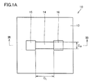
- FIG. 1A is a schematic plan view illustrating an example of a semiconductor device according to one embodiment of the present invention.
- 1B is a schematic cross-sectional view taken along line IB-IB shown in FIG. 1A.
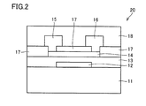
- FIG. 2 is a schematic cross-sectional view illustrating another example of a semiconductor device according to one embodiment of the present invention.
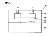
- FIG. 3 is a schematic cross-sectional view illustrating still another example of the semiconductor device according to one aspect of the present invention.
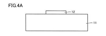
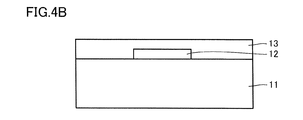
- 4A is a schematic cross-sectional view showing an example of a method for manufacturing the semiconductor device shown in FIG. 1A and FIG. 1B.
- 4B is a schematic cross-sectional view showing an example of a method for manufacturing the semiconductor device shown in FIG. 1A and FIG. 1B.
- FIG. 1A is a schematic plan view illustrating an example of a semiconductor device according to one embodiment of the present invention.
- 1B is a schematic cross-sectional view taken along line IB-IB shown in FIG. 1A.
- FIG. 4C is a schematic cross-sectional view showing an example of a method for manufacturing the semiconductor device shown in FIGS. 1A and 1B.
- FIG. 4D is a schematic cross-sectional view showing an example of a manufacturing method of the semiconductor device shown in FIGS. 1A and 1B.
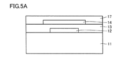
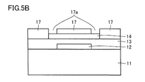
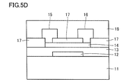
- FIG. 5A is a schematic cross-sectional view showing an example of a manufacturing method of the semiconductor device shown in FIG.
- FIG. 5B is a schematic cross-sectional view showing an example of a manufacturing method of the semiconductor device shown in FIG.
- FIG. 5C is a schematic cross-sectional view showing an example of a manufacturing method of the semiconductor device shown in FIG.
- FIG. 5D is a schematic cross-sectional view showing an example of a method for manufacturing the semiconductor device shown in FIG.
- the sputter target When an oxide sintered body is applied to a sputter target, the sputter target is generally processed into a desired shape by grinding, cutting, or the like. Since the oxide sintered body may be chipped or cracked during such processing, it is desirable that the oxide sintered body has high mechanical strength.
- an oxide sintered body that can exhibit high mechanical strength and high thermal conductivity, a method for manufacturing the oxide sintered body, a sputter target including the oxide sintered body, and the sputter target are used.
- An object is to provide a method for manufacturing a semiconductor device including an oxide semiconductor film to be formed.
- An oxide sintered body is an oxide sintered body containing indium (In), tungsten (W), and zinc (Zn), and the oxide sintered body Particles that are the main component and include the first crystal phase including the bixbite type crystal phase and the second crystal phase having a higher zinc content than the first crystal phase, and constituting the second crystal phase have an average length
- the shaft diameter is 3 ⁇ m or more and 50 ⁇ m or less, and the average aspect ratio is 4 or more and 50 or less.
- the second crystal phase is included in a part of the oxide sintered body.
- the oxide sintered body of the present embodiment can exhibit high mechanical strength and high thermal conductivity.
- the oxide sintered body of the present embodiment can exhibit a high apparent density (which means an apparent density after sintering and is also referred to as a sintered density) even at a relatively low sintering temperature.
- the oxide sintered body of this embodiment can be suitably used as a sputtering target for forming an oxide semiconductor film (for example, an oxide semiconductor film functioning as a channel layer) included in a semiconductor device. According to the oxide sintered body, a semiconductor device having high field effect mobility and high reliability can be obtained.
- the oxide sintered body of the present embodiment has a first diffraction peak at a position larger than 34.74 deg of 2 ⁇ in X-ray diffraction and smaller than 34.97 deg, and larger than 31.77 deg of 2 ⁇ and 32.00 deg.
- the second diffraction peak can be provided at a smaller position, and in this case, the ratio Ia / Ib between the peak intensity Ia of the first diffraction peak and the peak intensity Ib of the second diffraction peak is 0.05 or more and 3 or less. Is preferred.
- the Ia / Ib within this range is advantageous for realizing an oxide sintered body having a high apparent density and a high thermal conductivity even at a relatively low sintering temperature. It is also advantageous in increasing field effect mobility and reliability.
- the oxide sintered body of the present embodiment has an apparent density greater than 6.4 g / cm 3 and 7.5 g / cm 3 or less, and is based on the sum of indium, tungsten, and zinc in the oxide sintered body.
- the content of tungsten (hereinafter also referred to as “W content” of the oxide sintered body) is larger than 0.5 atomic% and not larger than 5.0 atomic%, and indium, tungsten and
- the zinc content relative to the total zinc (hereinafter also referred to as “Zn content” of the oxide sintered body) is 1.2 atomic% or more and less than 50 atomic%, and zinc relative to tungsten in the oxide sintered body
- the atomic ratio (hereinafter also referred to as “Zn / W ratio” of the oxide sintered body) is preferably larger than 1.0 and smaller than 100.
- the apparent density within the above range is advantageous when the oxide sintered body of the present embodiment is used as a sputtering target.
- the W content, Zn content, and Zn / W ratio being in the above ranges are advantageous for realizing an oxide sintered body that has a high apparent density and a high thermal conductivity even at a relatively low sintering temperature. It is also advantageous for enhancing the field effect mobility and reliability of the semiconductor device.
- a sputter target according to another embodiment of the present invention includes the oxide sintered body of the above embodiment. Since the sputter target of this embodiment includes the oxide sintered body of the above-described embodiment, it is preferably used for forming an oxide semiconductor film of a semiconductor device with high field effect mobility and high reliability by a sputtering method.
- a semiconductor device manufacturing method is a method for manufacturing a semiconductor device including an oxide semiconductor film, the step of preparing the sputter target of the above embodiment, and the sputter target. And forming the oxide semiconductor film by sputtering using a sputtering method. Since the semiconductor device obtained by the manufacturing method of this embodiment includes an oxide semiconductor film formed by sputtering using the sputtering target of the above embodiment, high field-effect mobility and reliability can be exhibited.
- the semiconductor device described here is not particularly limited, but a TFT (thin film transistor) including an oxide semiconductor film formed by a sputtering method using the sputtering target of the above embodiment as a channel layer is a preferable example.
- the content of tungsten with respect to the total of indium, tungsten, and zinc in the obtained oxide semiconductor film (hereinafter, also referred to as “W content” of the oxide semiconductor film).
- W content the content of tungsten with respect to the total of indium, tungsten, and zinc in the obtained oxide semiconductor film.
- Zn content ratio the zinc content relative to the total of indium, tungsten and zinc in the oxide semiconductor film
- Zn content ratio Is 1 atomic percent or more and less than 50 atomic percent
- the atomic ratio of zinc to tungsten in the oxide semiconductor film (hereinafter also referred to as “Zn / W ratio” of the oxide semiconductor film) is from 1.0. It is preferably larger and smaller than 100. Since the semiconductor device obtained by the manufacturing method of this embodiment includes an oxide semiconductor film formed using the sputtering target of the above embodiment, high field-effect mobility and reliability can be exhibited.
- the obtained oxide semiconductor film can be composed of at least one of a nanocrystalline oxide and an amorphous oxide. This is advantageous in increasing the field effect mobility and reliability in a semiconductor device including an oxide semiconductor film as a channel layer, for example.
- a method for manufacturing an oxide sintered body according to still another embodiment of the present invention is a method for manufacturing an oxide sintered body according to the above-described embodiment, and includes an indium oxide powder and a tungsten oxide powder.
- a step of preparing a primary mixture, a step of forming a calcined powder by heat-treating the primary mixture, a step of preparing a secondary mixture of raw material powders including the calcined powder, and forming the secondary mixture The step of forming a sintered body and the step of forming an oxide sintered body by sintering the molded body, and the step of forming the calcined powder is performed at 700 ° C. or higher and lower than 1400 ° C. in an oxygen-containing atmosphere.
- the mechanical strength and thermal conductivity are high, or in addition to these, oxide sintered bodies having a high apparent density even at a relatively low sintering temperature are compared. Can be easily obtained.
- the double oxide may include an In 6 WO 12 type crystal phase. This is advantageous in obtaining an oxide sintered body having high apparent density and mechanical strength and high thermal conductivity.
- a method for manufacturing an oxide sintered body according to still another embodiment of the present invention is a method for manufacturing an oxide sintered body according to the above-described embodiment, and includes a zinc oxide powder and a tungsten oxide powder.
- a step of preparing a primary mixture, a step of forming a calcined powder by heat-treating the primary mixture, a step of preparing a secondary mixture of raw material powders including the calcined powder, and forming the secondary mixture The step of forming a calcined powder including the step of forming a molded body by sintering and the step of forming an oxide sintered body by sintering the molded body is performed at 550 ° C. or more and less than 1200 ° C.
- an oxide sintered body of the present embodiment Forming a double oxide powder containing zinc and tungsten as the calcined powder by heat-treating the primary mixture at a temperature of According to the method for manufacturing an oxide sintered body of the present embodiment, the mechanical strength and thermal conductivity are high, or in addition to these, oxide sintered bodies having a high apparent density even at a relatively low sintering temperature are compared. Can be easily obtained.
- the double oxide may contain a ZnWO 4 type crystal phase. This is advantageous in obtaining an oxide sintered body having high apparent density and mechanical strength and high thermal conductivity.
- the tungsten oxide powder is selected from the group consisting of a WO 3 crystal phase, a WO 2 crystal phase, and a WO 2.72 crystal phase. It may contain at least one selected crystal phase. This is advantageous in obtaining an oxide sintered body having high apparent density and mechanical strength and high thermal conductivity.
- the tungsten oxide powder may have a median particle diameter d50 of 0.1 ⁇ m or more and 4 ⁇ m or less. This is advantageous in obtaining an oxide sintered body having high apparent density and mechanical strength and high thermal conductivity.
- the oxide sintered body of the present embodiment is an oxide sintered body containing indium (In), tungsten (W), and zinc (Zn).
- the oxide sintered body of the present embodiment includes a first crystal phase that is a main component of the oxide sintered body and includes a bixbite type crystal phase, and a second zinc content higher than that of the first crystal phase.
- the particles comprising the crystal phase and constituting the second crystal phase have an average major axis diameter of 3 ⁇ m or more and 50 ⁇ m or less, and an average aspect ratio of 4 or more and 50 or less.
- the second crystal phase is included in a part of the oxide sintered body.
- the oxide sintered body of the present embodiment can exhibit high mechanical strength and high thermal conductivity.
- the oxide sintered body of the present embodiment can be suitably used as a sputtering target for forming an oxide semiconductor film (for example, an oxide semiconductor film functioning as a channel layer) of a semiconductor device. According to the sintered body, it is possible to obtain a semiconductor device with high field effect mobility and high reliability.
- the first crystal phase is a main component of the oxide sintered body and is an indium high-content crystal phase described later including at least a bixbite type crystal phase.
- the “bixbite type crystal phase” means a bixbite crystal phase, and a phase in which at least one of the metal elements other than In is included in at least a part of the bixbite crystal phase, A generic term for those having the same crystal structure.
- the bixbite crystal phase is one of the crystal phases of indium oxide (In 2 O 3 ), refers to the crystal structure defined in JCPDS card 6-0416, and is a rare earth oxide C-type phase (or C-rare). Also called soil structure phase.
- bixbite type crystal phase can be identified by X-ray diffraction. That is, the existence of a bixbite type crystal phase is confirmed by X-ray diffraction, and the spacing between each plane can be measured.
- the measurement conditions for X-ray diffraction the conditions shown in the following “(3) X-ray diffraction characteristics of oxide sintered body” are adopted.
- the first crystal phase including the bixbite type crystal phase is the main component of the oxide sintered body” means that in the oxide sintered body, the bixbite type crystal phase, the indium tungstate compound crystal phase, etc. This means that the ratio of the indium-rich crystal phase containing In in terms of content (the indium-rich crystal phase occupancy) is 50% or more.
- the “indium-rich crystal phase occupancy” is measured as follows. First, a sample is taken from a part of the oxide sintered body, and the surface of the sample is polished and smoothed. Next, using SEM-EDX (scanning secondary electron microscope with an energy dispersive fluorescence X-ray analyzer), the surface of the sample is observed with SEM (scanning secondary electron microscope), and each crystal particle is observed. The metal elemental composition ratio is analyzed by EDX (energy dispersive fluorescence X-ray analyzer). Then, the crystal particles are grouped based on the tendency of the composition ratio of the metal elements of the crystal particles.
- SEM-EDX scanning secondary electron microscope with an energy dispersive fluorescence X-ray analyzer
- the Zn content rate [Zn content rate (atomic%) with respect to the sum of In, W, and Zn] is higher than the group B described later, and the Zn content rate is very low.
- Group B indium-rich crystal phase
- the crystal grains of group B are determined to be the first crystal phase (such as In 2 O 3 phase).
- the first crystal phase may include an indium tungstate compound crystal phase in addition to the bixbyite crystal phase.
- the “indium-rich crystal phase occupancy ratio” in the oxide sintered body is defined as the ratio (percentage) of the area of the indium-rich crystal phase (group B) to the measurement surface of the oxide sintered body. Is done.
- the oxide sintered body according to this embodiment including the first crystal phase (indium-rich crystal phase) as a main component has an indium-rich crystal phase occupancy of 50% or more according to this definition.
- W and / or Zn may be dissolved in at least a part thereof. This is advantageous in realizing an oxide sintered body having high mechanical strength and high thermal conductivity, and the oxide semiconductor film formed using the oxide sintered body is channeled. This is also advantageous in increasing the field effect mobility and reliability of the semiconductor device included as a layer.
- W and / or Zn is solid-dissolved in at least a part of the first crystal phase means that W and / or Zn is solid in a substitutional form in at least a part of the crystal lattice of the first crystal phase. It means a dissolved form, an interstitial solid solution form between crystal lattices, or a solid solution form in both substitutional and interstitial forms.
- the oxide sintered body according to the present embodiment when W and / or Zn is dissolved in at least a part of the bixbite type crystal phase included in the first crystal phase, it is defined in JCPDS card 6-0416. It becomes wider or narrower than the surface spacing. In X-ray diffraction, the peak position shifts to the high angle side or shifts to the low angle side. This peak shift is confirmed, and SEM-EDX (scanning secondary electron microscope with an energy dispersive fluorescent X-ray analyzer) and TEM-EDX (transmission with an energy dispersive fluorescent X-ray analyzer) are used.
- SEM-EDX scanning secondary electron microscope with an energy dispersive fluorescent X-ray analyzer
- TEM-EDX transmission with an energy dispersive fluorescent X-ray analyzer
- the bixbite type crystal phase contained in the first crystal phase contains W and / or Zn. It can be determined that is dissolved.
- the presence elements are identified using ICP (inductively coupled plasma) mass spectrometry, SEM-EDX, and other element identification methods, and the presence of W and / or Zn together with In is confirmed. It can also be determined that W and / or Zn is solid-solved in the bixbite type crystal phase contained in the first crystal phase when the oxide of W and / or Zn is not confirmed by diffraction.
- ICP inductively coupled plasma
- the first crystal phase may further include an indium tungstate compound crystal phase. Further including an indium tungstate compound crystal phase is advantageous in realizing an oxide sintered body having high mechanical strength and high thermal conductivity, and is formed using the oxide sintered body. This is also advantageous in improving the field effect mobility and reliability of a semiconductor device including the oxide semiconductor film to be used as a channel layer.
- the indium tungstate compound crystal phase is a phase that can be included in a part of the oxide sintered body.
- indium tungstate compound crystal phase is a crystal phase mainly composed of In, W and O.
- In 6 WO 12 crystal phase, InW 3 O 9 phase and the like can be mentioned.
- the In 6 WO 12 crystal phase is a crystal phase of an indium tungstate compound having a trigonal crystal structure and having a crystal structure defined in JCPDS card 01-074-1410.
- oxygen may be deficient or metal may be dissolved, and the lattice constant may be changed.
- the InW 3 O 9 phase has a hexagonal crystal structure and is an indium tungstate compound crystal phase having a crystal structure defined by JCPDS Card 33-627. As long as the crystal system is shown, oxygen may be deficient or metal may be dissolved, and the lattice constant may be changed.
- the presence of the indium tungstate compound crystal phase is confirmed by obtaining a peak attributed to the indium tungstate compound crystal phase in X-ray diffraction.
- the oxide sintered body of the present embodiment has a higher Zn content (Zn content (atomic%) relative to the sum of In, W, and Zn) than the first crystal phase. Further comprising a phase.
- the second crystal phase is a phase included in a part of the oxide sintered body.
- the second crystal phase preferably has a Zn content of 50 atomic% or more. From the viewpoint of realizing an oxide sintered body having high mechanical strength and high thermal conductivity, the Zn content of the second crystal phase is more preferably 60 atomic% or more, and further preferably 70 atomic%. That's it.
- the Zn content of the second crystal phase may be 100 atomic%.
- the presence of the second crystal phase can be confirmed by surface analysis using SEM-EDX performed when obtaining the indium-rich crystal phase occupancy ratio.
- the crystal phase constituting the crystal particles is the second crystal phase.
- the second crystal phase can be, for example, a hexagonal wurtzite crystal phase, a zinc tungstate compound crystal phase, a hexagonal layered crystal phase, and combinations thereof.
- the term “hexagonal wurtzite crystal phase” refers to a hexagonal wurtz crystal phase and a phase in which at least part of the hexagonal wurtz crystal phase contains at least one metal element other than Zn, A generic term for those having the same crystal structure as the Wurtz crystal phase.
- the hexagonal wurtz crystal phase is one of the crystal phases of zinc oxide (ZnO), and space group: P63mc, space group no. : A crystal structure represented by 186 and defined in JCPDS card 01-079-0207. The presence of the hexagonal wurtzite crystal phase can be confirmed by obtaining a peak attributed to the hexagonal wurtzite crystal phase in X-ray diffraction.
- the hexagonal wurtzite crystal phase may contain ZnO as a main component, and W and / or In may be dissolved in substitutional or interstitial forms at least in part.
- W and / or In may be dissolved in substitutional or interstitial forms at least in part.
- the “zinc tungstate compound crystal phase” is a crystal phase mainly composed of Zn, W and O.
- a ZnWO 4 type crystal phase can be mentioned.
- the "ZnWO 4 type crystal phase”, ZnWO 4 crystalline phase, and at least a portion of ZnWO 4 crystalline phase a phase that contains at least one element other than Zn and W, the same crystal structure as ZnWO 4 crystalline phase This is a general term for those having The ZnWO 4 crystal phase is a zinc tungstate compound crystal phase having a crystal structure represented by the space group P12 / c1 (13) and having a crystal structure defined by JCPDS card 01-088-0251. As long as the crystal system is shown, oxygen may be deficient or metal may be dissolved, and the lattice constant may be changed.
- the presence of the zinc tungstate compound crystal phase can be confirmed by obtaining a peak attributed to the zinc tungstate compound crystal phase in X-ray diffraction. Further, the abundance ratio can be confirmed by surface analysis using SEM-EDX, which is performed when obtaining the indium-rich crystal phase occupation ratio. Specifically, in the above-mentioned group A grouped by this surface analysis, crystal grains containing Zn and W, more typically Zn content [Zn content relative to the sum of In, W and Zn ( Atomic%)] and W content [W content (atomic%) with respect to the sum of In, W, and Zn] are mixed at a ratio close to that of the zinc tungstate compound crystal phase in the aforementioned X-ray diffraction. The zinc tungstate compound crystal phase can be confirmed and the abundance ratio can be confirmed.
- Examples of the hexagonal layered crystal phase include In 2 O 3 (ZnO) 5 .
- the presence of a hexagonal layered crystal phase such as In 2 O 3 (ZnO) 5 can be confirmed by obtaining a peak attributed to the hexagonal layered crystal phase in X-ray diffraction.
- the hexagonal layered crystal may contain W and / or In as a solid solution in at least a part thereof in a substitutional or interstitial form.
- X-ray diffraction, SEM-, and the like as in the method for confirming that “W and / or Zn is dissolved in at least a part of the first crystal phase” described above.
- a technique using EDX, TEM-EDX can be applied.
- the presence of the second crystal phase can be confirmed by surface analysis using SEM-EDX performed when obtaining the indium-rich crystal phase occupancy, and is grouped by this surface analysis.
- the crystal phase constituting the group A crystal grains is the second crystal phase. That is, it can be determined that the second crystal phase is included when there is a region where the Zn content is higher than that of the first crystal phase.
- the second crystal phase may be a crystal phase other than the hexagonal wurtzite crystal phase, the zinc tungstate compound crystal phase, and the hexagonal layered crystal phase mentioned above.
- the crystal grains constituting the second crystal phase preferably have an average major axis diameter of 3 to 50 ⁇ m and an average aspect ratio of 4 to 50. This is advantageous in realizing an oxide sintered body having high mechanical strength and high thermal conductivity, and the oxide semiconductor film formed using the oxide sintered body is channeled. This is also advantageous in increasing the field effect mobility and reliability of the semiconductor device included as a layer.
- the average major axis diameter and average aspect ratio are obtained as follows.
- group A which is the second crystal phase
- group B which is the second crystal phase
- the major axis length and minor axis length of the crystal grains constituting the second crystal phase observed in dark gray in the backscattered electron image taken at 500 times are measured, and the ratio of the major axis length to the minor axis length (long The aspect ratio is calculated (axis length / short axis length).
- the minor axis length is measured at a position that is 1/2 the major axis length.
- the second crystal phase to be measured does not have to be a single crystal, and may be a particle in which polycrystals are gathered together.
- One region of the independent second crystal phase surrounded by the first crystal phase is a single region. Measure as one particle.
- 100 short axis lengths and 100 long axis lengths of the second crystal phase in the 170 ⁇ m ⁇ 250 ⁇ m visual field of the backscattered electron image taken at 500 times are measured at random, and the long axis length is measured in order from the longest.
- the average value of 20 from the 3rd position to the 22nd position arranged in the above is defined as the average major axis diameter.
- An average major axis diameter of 3 ⁇ m or more and 50 ⁇ m or less is advantageous in increasing the mechanical strength and thermal conductivity of the oxide sintered body.
- the average major axis diameter is preferably 10 ⁇ m or more, more preferably 15 ⁇ m or more.
- the average major axis diameter is preferably 40 ⁇ m or less, more preferably 30 ⁇ m or less.
- An average aspect ratio of 4 or more and 50 or less is advantageous for increasing the mechanical strength and also advantageous for increasing the thermal conductivity.
- the average aspect ratio is less than 4, sufficiently high mechanical strength and thermal conductivity cannot be obtained.
- the average aspect ratio is larger than 50, a sufficiently high apparent density cannot be obtained, so that the mechanical strength is lowered.
- the average aspect ratio is preferably 6 or more, more preferably 8 or more.
- the average aspect ratio is preferably 40 or less, more preferably 30 or less.
- the oxide sintered body of the present embodiment has a first diffraction peak at a position larger than 34.74 deg of 2 ⁇ in X-ray diffraction and smaller than 34.97 deg. 2 ⁇ has a second diffraction peak at a position larger than 31.77 deg and smaller than 32.00 deg, and the ratio Ia / Ib between the peak intensity Ia of the first diffraction peak and the peak intensity Ib of the second diffraction peak is 0.05 or more. It is preferable that it is 3 or less.
- This range of Ia / Ib is advantageous in realizing an oxide sintered body having a high apparent density and a high thermal conductivity even at a relatively low sintering temperature. This is also advantageous in increasing the field-effect mobility and reliability of a semiconductor device including an oxide semiconductor film formed using a combined body as a channel layer.
- the first diffraction peak and the second diffraction peak may be obtained from the same crystal phase. If the first diffraction peak and the second diffraction peak are not obtained from the same crystal phase, the crystal phase having the second diffraction peak may be In 2 O 3 (ZnO) 5. is not.
- Ia / Ib When Ia / Ib is less than 0.05, the thermal conductivity of the obtained oxide sintered body tends not to be sufficiently high. From this viewpoint, Ia / Ib is more preferably 0.1 or more, and further preferably 0.2 or more. It is not easy to prepare an oxide sintered body having Ia / Ib greater than 3. From the viewpoint of obtaining high thermal conductivity, Ib / Ia is more preferably 2 or less.
- the X-ray diffraction measurement is performed under the following conditions or equivalent conditions.
- Measurement conditions for X-ray diffraction ⁇ -2 ⁇ method, X-ray source: Cu K ⁇ ray, X-ray tube voltage: 45 kV, X-ray tube current: 40 mA, Step width: 0.03 deg. Step time: 1 second / step, Measurement range 2 ⁇ : 10 deg to 90 deg.
- Ia / Ib shows a value specific to the material when the sample is non-oriented, but in the oxide sintered body of the present embodiment, Ia / Ib may show a value different from the value specific to the material. .
- the second crystal phase is considered to have orientation.
- the thermal conductivity and mechanical strength of the oxide sintered body may vary depending on the crystal orientation, but in the oxide sintered body of this embodiment, Ia / Ib is high when it is 0.05 or more and 3 or less. This is advantageous in realizing thermal conductivity and high mechanical strength.
- the oxide sintered body of the present embodiment has an apparent density greater than 6.4 g / cm 3 and 7.5 g / It is preferable that it is cm 3 or less.
- the oxide sintered body of the present embodiment preferably has a relative density (relative density / theoretical density) of 94% or more, which is the ratio of the apparent density to the theoretical density.
- the apparent density within the above range is advantageous when the oxide sintered body of the present embodiment is used as a sputtering target.
- the apparent density of the oxide sintered body is preferably as high as possible.
- the low apparent density of the oxide sintered body means that there are many voids in the oxide sintered body.
- the sputter target is used while its surface is etched with argon ions during use. Therefore, if there are vacancies in the oxide sintered body, they are exposed during film formation and the internal gas is released, so that the gas released from the target is mixed into the deposited oxide semiconductor thin film. As a result, the film characteristics deteriorate.
- the oxide sintered body of the present embodiment has a W content greater than 0.5 atomic% and 5.0 atomic% or less, a Zn content of 1.2 atomic% or more and less than 50 atomic%, and Zn /
- the W ratio is preferably larger than 1.0 and smaller than 100.
- the W content, Zn content, and Zn / W ratio being in the above ranges are advantageous for realizing an oxide sintered body that has a high apparent density and a high thermal conductivity even at a relatively low sintering temperature.
- the W content of the oxide sintered body is more preferably 0.6 atomic% or more and 3 atomic% or less, and further preferably 2 atomic% or less.
- the W content of the oxide sintered body is 0.5 atomic% or less, in a semiconductor device including an oxide semiconductor film formed using the oxide sintered body as a channel layer, the reliability becomes low. End up.
- the W content of the oxide sintered body exceeds 5 atomic%, in a semiconductor device including an oxide semiconductor film formed using a sputtering target including the oxide sintered body as a channel layer, field effect mobility Will be lower.
- the range of the W content of the oxide sintered body is determined by the characteristics of the semiconductor device including the oxide semiconductor film formed using the oxide sintered body of the present embodiment as a channel layer.
- the W content of the oxide semiconductor film usually indicates a value corresponding to the W content of the oxide sintered body.
- the W content of the oxide semiconductor film does not necessarily match the W content of the oxide sintered body.
- An oxide sintered body obtained by mixing indium oxide and tungsten oxide generally has a small apparent density.
- the apparent density can be increased by containing Zn and increasing the contact points between W and Zn
- the desired W content determined in consideration of the characteristics of the semiconductor device is greater than 0.5 atomic%. Since the amount is as small as 0 atomic% or less, it is preferable to increase the Zn content in order to realize an oxide sintered body having a higher apparent density.
- the Zn content is less than 1.2 atomic%, it tends to be difficult to obtain a sufficiently high apparent density.
- the Zn content is 50 atomic% or more, the electric resistance of the oxide sintered body increases, and it tends to be difficult to perform sputtering by applying a DC voltage.
- the crystal grains constituting the second crystal phase are connected to each other, and it is difficult to confirm by measurement whether the average major axis diameter and / or the average aspect ratio are in the predetermined range.
- the Zn / W ratio is 1.0 or less, it tends to be difficult to obtain a sufficiently high apparent density.
- the Zn / W ratio is 100 or more, the electric resistance of the oxide sintered body is high, and it tends to be difficult to perform sputtering by applying a DC voltage.
- the contents of In, Zn, and W in the oxide sintered body can be measured by ICP mass spectrometry.
- the oxide sintered body of the present embodiment may further contain zirconium (Zr).
- the content is, for example, 1 ⁇ 10 17 atms / cm 3 or more and 1 ⁇ 10 20 atms / cm 3 or less.
- Zr is an element that can be mixed in the manufacturing process of the oxide sintered body, but does not hinder achieving a high apparent density and a high mechanical strength. The presence of Zr and its content can be confirmed with a secondary ion mass spectrometer.
- the oxide sintered body of the present embodiment can be suitably used as a sputter target.
- the sputter target is a raw material for the sputtering method.
- a sputtering target and a substrate are placed facing each other in a film forming chamber, a voltage is applied to the sputtering target, and the surface of the target is sputtered with rare gas ions, thereby forming atoms constituting the target from the target.
- This is a method of forming a film composed of atoms constituting the target by releasing and depositing on the substrate.
- the sputter target is heated because a current flows by the applied voltage. For this reason, the oxide sintered body is generally attached to a copper backing plate with indium metal and water-cooled from the copper side.
- the oxide sintered body of the present embodiment is an oxide sintered body having high thermal conductivity and high mechanical strength that meets such requirements, in particular by having a predetermined average major axis diameter and average aspect ratio. .
- One method for producing an oxide sintered body according to this embodiment is a method for producing an oxide sintered body according to Embodiment 1, in which a primary mixture of zinc oxide powder and tungsten oxide powder is used.
- a step of preparing, a step of forming a calcined powder by heat-treating the primary mixture, a step of preparing a secondary mixture of raw material powders including the calcined powder, and a molded body by molding the secondary mixture A step of forming, and a step of forming an oxide sintered body by sintering the formed body.
- the primary mixture is heat-treated at a temperature of 550 ° C. or higher and lower than 1200 ° C. in an oxygen-containing atmosphere, thereby forming a double oxide powder containing Zn and W as the calcined powder. Including that.
- the primary mixture of the zinc oxide powder and the tungsten oxide powder is heat-treated at a temperature of 550 ° C. or more and less than 1200 ° C. in an oxygen-containing atmosphere.
- a temperature of 550 ° C. or more and less than 1200 ° C. in an oxygen-containing atmosphere is formed as the calcined powder.
- an oxide sintered body that has high mechanical strength and high thermal conductivity and can be suitably used as a sputtering target is obtained. be able to.
- an oxide sintered body having a high apparent density can be obtained even at a relatively low sintering temperature.
- the double oxide may be deficient in oxygen or substituted with metal.
- the temperature of the heat treatment is less than 550 ° C., a double oxide powder containing Zn and W cannot be obtained, and if it is 1200 ° C. or higher, the double oxide powder containing Zn and W is decomposed or scattered. The particle size of the double oxide powder tends to be too large for use.
- an oxide semiconductor film formed using a sputter target containing an oxide sintered body obtained is formed into a channel layer.
- the semiconductor device including the field effect mobility and reliability can be increased more effectively.
- the double oxide containing Zn and W preferably contains a ZnWO 4 type crystal phase.
- the ZnWO 4 type crystal phase is a zinc tungstate compound crystal phase having a crystal structure represented by the space group P12 / c1 (13) and having a crystal structure defined by JCPDS card 01-088-0251. . As long as the crystal system is shown, oxygen may be deficient or metal may be dissolved, and the lattice constant may be changed.
- the ZnWO 4 type crystal phase is identified by X-ray diffraction measurement.
- another one of the manufacturing methods of the oxide sintered compact which concerns on this embodiment is a manufacturing method of the oxide sintered compact which concerns on Embodiment 1, Comprising: Indium oxide powder and tungsten oxide powder
- a step of preparing a primary mixture, a step of forming a calcined powder by heat-treating the primary mixture, a step of preparing a secondary mixture of raw material powders including the calcined powder, and forming the secondary mixture The step of forming a molded body by the above and the step of forming an oxide sintered body by sintering the molded body are included.
- the primary mixture is heat-treated at a temperature of 700 ° C. or higher and lower than 1400 ° C. in an oxygen-containing atmosphere, thereby forming a double oxide powder containing In and W as the calcined powder. Including that.
- the primary mixture of the indium oxide powder and the tungsten oxide powder is heat-treated at a temperature of 700 ° C. or higher and lower than 1400 ° C. in an oxygen-containing atmosphere.
- a double oxide powder containing In and W as the calcined powder provides an oxide sintered body that has high mechanical strength and high thermal conductivity and can be suitably used as a sputtering target. be able to.
- an oxide sintered body having a high apparent density can be obtained even at a relatively low sintering temperature.
- the double oxide may be deficient in oxygen or substituted with metal.
- the heat treatment temperature is less than 700 ° C., a double oxide powder containing In and W cannot be obtained. If the heat treatment temperature is 1400 ° C. or higher, the double oxide powder containing In and W is decomposed or scattered. The particle size of the double oxide powder tends to be too large for use.
- an oxide semiconductor film formed using a sputter target containing an oxide sintered body obtained is formed into a channel layer.
- the semiconductor device including the field effect mobility and reliability can be increased more effectively.
- the double oxide containing In and W preferably contains an In 6 WO 12 type crystal phase.
- the In 6 WO 12 crystal phase is a crystal phase of an indium tungstate compound having a trigonal crystal structure and having a crystal structure defined in JCPDS card 01-074-1410. As long as the crystal system is shown, oxygen may be deficient or metal may be dissolved, and the lattice constant may be changed.
- the indium tungstate compound crystal phase disclosed in Japanese Patent Application Laid-Open No. 2004-091265 is an InW 3 O 9 crystal phase, has a hexagonal crystal structure, and is defined in JCPDS Card 33-627. The crystal structure is different from the In 6 WO 12 crystal phase.
- In 6 WO 12 type crystal phase is identified by X-ray diffraction measurement.
- the oxide sintered body containing In, W and Zn In order to increase the apparent density of the oxide sintered body containing In, W and Zn, it is effective to have a double oxide containing Zn and W having a low melting point present during sintering.
- a method of using a composite oxide powder containing Zn and W synthesized in advance in a manufacturing process and a method using a composite oxide powder containing indium and tungsten synthesized beforehand may be used in combination.
- a method of using a composite oxide powder containing Zn and W synthesized in advance in a manufacturing process and a method using a composite oxide powder containing indium and tungsten synthesized beforehand may be used in combination.
- the tungsten oxide powder used for manufacturing the oxide sintered body includes at least one crystal phase selected from the group consisting of a WO 3 crystal phase, a WO 2 crystal phase, and a WO 2.72 crystal phase.
- the apparent density and mechanical strength of the oxide sintered body can be increased more effectively, and it is advantageous for increasing the field effect mobility and reliability.
- the tungsten oxide powder preferably has a median particle diameter d50 of 0.1 ⁇ m to 4 ⁇ m, more preferably 0.2 ⁇ m to 2 ⁇ m, and further preferably 0.3 ⁇ m to 1.5 ⁇ m. preferable. Thereby, the apparent density and mechanical strength of the oxide sintered body can be increased more effectively.
- the median particle size d50 is determined by BET specific surface area measurement. When the median particle size d50 is smaller than 0.1 ⁇ m, it is difficult to handle the powder, and it tends to be difficult to uniformly mix the zinc oxide powder and the tungsten oxide powder or the indium oxide powder and the tungsten oxide powder. .
- the mixed oxide powder containing Zn and W obtained by heat treatment at a temperature of 550 ° C. or more and less than 1200 ° C. in an oxygen-containing atmosphere after mixing with the zinc oxide powder The particle size also increases, and it tends to be difficult to increase the apparent density and mechanical strength of the oxide sintered body.
- the particle size of the double oxide powder containing In and W obtained by heat treatment at a temperature of 700 ° C. or higher and lower than 1400 ° C. in an oxygen-containing atmosphere after being mixed with the indium oxide powder is also increased. Therefore, it tends to be difficult to increase the apparent density and mechanical strength of the oxide sintered body.
- the manufacturing method of the oxide sintered body according to the present embodiment is not particularly limited, but includes, for example, the following steps from the viewpoint of efficiently forming the oxide sintered body of Embodiment 1.
- Indium oxide powder for example, In 2 O 3 powder
- tungsten oxide powder for example, WO 3 powder, WO 2.72 powder, WO 2 powder
- a metal element oxide powder constituting the oxide sintered body such as zinc oxide powder (for example, ZnO powder)
- the tungsten oxide powder it is possible to use not only WO 3 powder but also powder having a chemical composition deficient in oxygen as compared with WO 3 powder such as WO 2.72 powder and WO 2 powder as a raw material. It is preferable from the viewpoint of improving mobility and reliability.
- the purity of the raw material powder is preferably a high purity of 99.9% by mass or more from the viewpoint of preventing unintentional mixing of metal elements and Si into the oxide sintered body and obtaining stable physical properties.
- the median particle diameter d50 of the tungsten oxide powder is preferably 0.1 ⁇ m or more and 4 ⁇ m or less from the viewpoint of increasing the apparent density and mechanical strength of the oxide sintered body.
- Step of preparing primary mixture (2-1) Step of preparing primary mixture of zinc oxide powder and tungsten oxide powder Among the above raw material powders, zinc oxide powder and tungsten oxide powder Mix (or pulverize and mix). At this time, when it is desired to obtain a ZnWO 4 type crystal phase as the crystal phase of the oxide sintered body, the tungsten oxide powder and the zinc oxide powder are mixed at a molar ratio of 1: 1 to Zn 2 W 3 O 8. In order to obtain a type crystal phase, the tungsten oxide powder and the zinc oxide powder are mixed at a molar ratio of 3: 2.
- the oxide sintered body is made of ZnWO. It preferably contains a type 4 phase.
- any of dry and wet methods may be used, and specifically, pulverized and mixed using a ball mill, a planetary ball mill, a bead mill or the like. Is done. In this way, a primary mixture of raw material powders is obtained.
- a drying method such as natural drying or a spray dryer can be used to dry the mixture obtained using the wet pulverization and mixing method.
- Step of preparing a primary mixture of indium oxide powder and tungsten oxide powder Among the raw material powders, indium oxide powder and tungsten oxide powder are mixed (or ground and mixed). At this time, when it is desired to obtain an In 6 WO 12 type crystal phase as the crystal phase of the oxide sintered body, the tungsten oxide powder and the indium oxide powder are mixed at a molar ratio of 1: 3.
- the method of mixing the tungsten oxide powder and the indium oxide powder and any of dry and wet methods may be used. Specifically, pulverized and mixed using a ball mill, a planetary ball mill, a bead mill or the like. Is done. In this way, a primary mixture of raw material powders is obtained.
- a drying method such as natural drying or a spray dryer can be used to dry the mixture obtained using the wet pulverization and mixing method.
- Step of forming calcined powder (3-1) Step of forming calcined powder of zinc tungstate oxide
- the obtained primary mixture is heat-treated (calcined) to obtain calcined powder (Zn and W A double oxide powder).
- the calcining temperature of the primary mixture is preferably less than 1200 ° C. so that the particle size of the calcined product becomes too large and the apparent density of the sintered body does not decrease.
- Zn and W are used as calcined products.
- the temperature is preferably 550 ° C. or higher.
- the calcining atmosphere may be an atmosphere containing oxygen, but may be an air atmosphere having a pressure higher than atmospheric pressure or air, or an oxygen-nitrogen mixed atmosphere containing 25% by volume or more of oxygen having a pressure higher than atmospheric pressure or air. preferable. Since the productivity is high, an air atmosphere at atmospheric pressure or in the vicinity thereof is more preferable.
- Step of forming a calcined powder of indium tungstate oxide The obtained primary mixture is heat-treated (calcined) to form a calcined powder (a double oxide powder containing In and W). To do.
- the calcining temperature of the primary mixture is preferably less than 1400 ° C. so that the particle size of the calcined product becomes too large and the apparent density or mechanical strength of the sintered body does not decrease.
- the temperature is preferably 700 ° C. or higher. More preferably, it is 800 degreeC or more and less than 1300 degreeC.
- the calcining atmosphere may be an atmosphere containing oxygen, but may be an air atmosphere having a pressure higher than atmospheric pressure or air, or an oxygen-nitrogen mixed atmosphere containing 25% by volume or more of oxygen having a pressure higher than atmospheric pressure or air. preferable. Since the productivity is high, an air atmosphere at atmospheric pressure or in the vicinity thereof is more preferable.
- Step of preparing a secondary mixture of raw material powder including calcined powder Next, the obtained calcined powder and the remaining powder of the raw material powder [indium oxide powder (for example, In 2 O 3 powder) ) Or zinc oxide powder (for example, ZnO powder)] is mixed (or ground and mixed) in the same manner as the preparation of the primary mixture. In this way, a secondary mixture of raw material powders is obtained.
- the tungsten oxide is preferably present as a double oxide by the calcination step.
- the obtained molded body is sintered to form an oxide sintered body.
- the hot press sintering method it is preferable not to use the hot press sintering method in terms of productivity.
- the sintering temperature of the molded body but in order to increase the apparent density of the oxide sintered body to be formed above 6.4 g / cm 3 and to increase the mechanical strength, the temperature is 900 ° C. or higher and 1200 ° C. It is preferable that the temperature is lower than ° C.
- the sintering atmosphere but from the viewpoint of preventing the generation of cracks by preventing the grain size of the constituent crystals of the oxide sintered body from increasing, an air atmosphere at or near atmospheric pressure is preferable. .
- the sputter target according to the present embodiment includes the oxide sintered body according to the first embodiment. Therefore, the sputter target according to this embodiment can be suitably used for forming an oxide semiconductor film of a semiconductor device having high field effect mobility and high reliability by a sputtering method.
- the sputter target according to this embodiment is preferably used for forming an oxide semiconductor film of a semiconductor device with high field effect mobility and high reliability by a sputtering method. It is preferable that a bonded body is included, and it is more preferable that the oxide sintered body of Embodiment 1 is included.
- the semiconductor device 10 according to the present embodiment is formed using the oxide sintered body according to the first embodiment, or formed by sputtering using the sputter target according to the third embodiment.
- An oxide semiconductor film 14 is included. Since the oxide semiconductor film 14 is included, the semiconductor device according to this embodiment can have characteristics of high field-effect mobility and high reliability.
- the semiconductor device 10 according to the present embodiment is not particularly limited, but is preferably a TFT (thin film transistor) because it has high field effect mobility and high reliability, for example.
- the oxide semiconductor film 14 included in the TFT is preferably a channel layer because it has high field-effect mobility and high reliability.
- the W content of the oxide semiconductor film 14 is preferably greater than 0.5 atomic% and equal to or less than 5.0 atomic%, and the Zn content of the oxide semiconductor film 14 is The Zn / W ratio of the oxide semiconductor film 14 is preferably greater than 1.0 and less than 100. Thereby, the field effect mobility and reliability of the semiconductor device 10 can be improved.
- the W content of the oxide semiconductor film 14 is more preferably 0.6 atomic percent or more and 3 atomic percent or less, and further preferably 2 atomic percent or less.
- the W content of the oxide semiconductor film 14 is 0.5 atomic% or less, the reliability of the semiconductor device including the oxide semiconductor film 14 as a channel layer is lowered.
- the W content of the oxide semiconductor film 14 exceeds 5 atomic%, field effect mobility is lowered in a semiconductor device including the oxide semiconductor film as a channel layer.
- the oxide semiconductor film 14 has a Zn content of 1 atomic% or more and less than 50 atomic% and the oxide semiconductor film 14 has a Zn / W ratio greater than 1.0 and less than 100, the oxide semiconductor film 14 is In a semiconductor device including a channel layer, field effect mobility can be increased and reliability can be increased.
- the Zn content of the oxide semiconductor film 14 is more preferably greater than 3 atomic% and less than or equal to 40 atomic%, and even more preferably greater than or equal to 5 atomic% and greater than 20 atomic%. small.
- the Zn content of the oxide semiconductor film 14 is smaller than 1 atomic%, the reliability of the semiconductor device including the oxide semiconductor film 14 as a channel layer is lowered.
- the Zn content of the oxide semiconductor film 14 is 50 atomic% or more, field effect mobility is lowered in a semiconductor device including the oxide semiconductor film 14 as a channel layer.
- the Zn / W ratio in the oxide semiconductor film 14 is 1.0 or less, the reliability of the semiconductor device including the oxide semiconductor film 14 as a channel layer is lowered.
- the Zn / W ratio is more preferably 3.0 or more, and further preferably 5.0 or more.
- the Zn / W ratio in the oxide semiconductor film 14 is 100 or more, field effect mobility is lowered in a semiconductor device including the oxide semiconductor film 14 as a channel layer.
- the Zn / W ratio is more preferably less than 20.
- the chemical composition of the oxide semiconductor film 14, that is, the content of various elements is measured by RBS (Rutherford backscattering analysis). Based on this measurement result, W content rate, Zn content rate, and Zn / W ratio are calculated.
- RBS Rutherford backscattering analysis
- W content rate, Zn content rate, and Zn / W ratio are calculated.
- TEM-EDX a transmission electron microscope with an energy dispersive fluorescent X-ray analyzer.
- RBS measurement is desirable because of the accuracy of chemical composition measurement.
- TEM-EDX first, a calibration curve sample is made of In, W, Zn, and O, has a composition close to the oxide semiconductor film to be measured, and can be analyzed by RBS At least three or more oxide semiconductor films are prepared.
- the contents of In, W and Zn are measured by RBS, and the contents of In, W and Zn are measured by TEM-EDX. From these measured values, a calibration curve showing the relationship between the measured values of In, W and Zn contents by TEM-EDX and the measured values of In, W and Zn contents by RBS is created. Then, for the oxide semiconductor film to be measured, the contents of In, W and Zn are measured by TEM-EDX, and then the measured values are measured for the contents of In, W and Zn by RBS based on the calibration curve. Convert to value. This converted value is the content of In, W, and Zn in the oxide semiconductor film to be measured.
- the oxide semiconductor 14 may further contain zirconium (Zr).
- the content is, for example, 1 ⁇ 10 17 atms / cm 3 or more and 1 ⁇ 10 20 atms / cm 3 or less.
- Zr is an element that can be mixed in the manufacturing process of the oxide sintered body, and can also be mixed in the oxide semiconductor film 14 formed using this oxide sintered body as a raw material. It does not hinder high field effect mobility and high reliability. The presence and content of zirconium can be confirmed with a secondary ion mass spectrometer.
- an oxide semiconductor changes the reliability of a semiconductor device by changing a sputtering power during the manufacture of the semiconductor device.
- the reliability of the semiconductor device is improved.
- the reason why the reliability can be increased is not clear, but it is conceivable that the density of the obtained oxide semiconductor film is improved and the density of trapped states of carriers that affect the reliability of the semiconductor device is decreased.
- the oxide semiconductor film 14 is composed of at least one of a nanocrystalline oxide and an amorphous oxide, and has a high field effect mobility in a semiconductor device (for example, TFT) including this as a channel layer, and This is preferable because the reliability can be increased.
- a semiconductor device for example, TFT
- the “nanocrystalline oxide” means that only a broad peak appearing on a low angle side called a halo is observed without observing a peak due to a crystal even by X-ray diffraction measurement according to the following conditions.
- region is implemented according to the following conditions using a transmission electron microscope, the ring-shaped pattern is observed.
- the ring-shaped pattern includes a case where spots are gathered to form a ring-shaped pattern.
- amorphous oxide means that only a broad peak appearing on the low angle side called a halo is observed without a peak due to a crystal being observed even by X-ray diffraction measurement under the following conditions.
- Measuring method Micro electron diffraction method, Acceleration voltage: 200 kV, Beam diameter: Same or equivalent to the thickness of the oxide semiconductor film to be measured.
- an oxide semiconductor film as disclosed in, for example, Japanese Patent No. 5172918 includes c-axis-oriented crystals along a direction perpendicular to the surface of the film. When the nanocrystals in the region are oriented in a certain direction, a spot-like pattern is observed.
- the nanocrystal has a crystal with respect to the surface of the film when at least a plane (film cross section) perpendicular to the film plane is observed. It is non-oriented and has random orientation. That is, the crystal axis is not oriented with respect to the film thickness direction.
- the oxide semiconductor film 14 is composed of nanocrystalline oxide or amorphous oxide, high field effect mobility can be achieved in a semiconductor device including the oxide semiconductor film 14 as a channel layer.
- the oxide semiconductor film 14 is preferably made of an amorphous oxide.
- the film thickness of the oxide semiconductor film 14 is, for example, not less than 2 nm and not more than 60 nm.
- the oxide semiconductor film 14 preferably has an electrical resistivity of 10 ⁇ 1 ⁇ cm or more.
- Many transparent conductive films using indium oxide have been studied so far, but the electrical resistivity is required to be smaller than 10 ⁇ 1 ⁇ cm in applications of these transparent conductive films.
- the oxide semiconductor film included in the semiconductor device of this embodiment preferably has an electric resistivity of 10 ⁇ 1 ⁇ cm or more, and thus can be suitably used as a channel layer of the semiconductor device. When the electrical resistivity is less than 10 ⁇ 1 ⁇ cm, it is difficult to use as a channel layer of a semiconductor device.
- the oxide semiconductor film 14 can be obtained by a manufacturing method including a step of forming a film by a sputtering method.
- the meaning of the sputtering method is as described above.
- a method for forming the oxide semiconductor film a pulse laser deposition (PLD) method, a heating deposition method, and the like have been proposed in addition to the sputtering method.
- PLD pulse laser deposition
- the sputtering method is preferable from the viewpoint of productivity.
- a magnetron sputtering method As the sputtering method, a magnetron sputtering method, a counter target type magnetron sputtering method, or the like can be used.
- Ar gas, Kr gas, and Xe gas can be used as the atmosphere gas at the time of sputtering, and oxygen gas can be mixed and used with these gases.
- the oxide semiconductor film 14 can also be obtained by heat treatment after film formation by sputtering, or by heat treatment while film formation by sputtering. Accordingly, an oxide semiconductor film composed of nanocrystalline oxide or amorphous oxide can be easily obtained. In addition, an oxide semiconductor film obtained by this method is advantageous in increasing field effect mobility and reliability in a semiconductor device (for example, TFT) including the oxide semiconductor film as a channel layer.
- a semiconductor device for example, TFT
- the heat treatment that is performed while performing film formation by sputtering can be performed by heating the substrate during the film formation.
- the substrate temperature is preferably 100 ° C. or higher and 250 ° C. or lower.
- the heat treatment time corresponds to the film formation time, and the film formation time depends on the thickness of the oxide semiconductor film 14 to be formed, but can be, for example, about 10 seconds to 10 minutes.
- the heat treatment performed after the film formation by the sputtering method can be performed by heating the substrate.
- heat treatment is preferably performed after film formation by sputtering.
- heat treatment may be performed immediately after the oxide semiconductor film 14 is formed, or heat treatment may be performed after the source electrode, the drain electrode, the etch stopper layer (ES layer), the passivation layer, and the like are formed. .
- the substrate temperature is preferably 100 ° C. or higher and 500 ° C. or lower.
- the atmosphere of the heat treatment may be various atmospheres such as air, nitrogen gas, nitrogen gas-oxygen gas, Ar gas, Ar-oxygen gas, water vapor-containing air, water vapor-containing nitrogen.
- the atmospheric pressure can be atmospheric pressure, reduced pressure conditions (for example, less than 0.1 Pa), and pressurized conditions (for example, 0.1 Pa to 9 MPa), but is preferably atmospheric pressure.
- the heat treatment time can be, for example, about 3 minutes to 2 hours, and preferably about 10 minutes to 90 minutes.
- 1A, 1B, 2 and 3 are schematic views showing some examples of a semiconductor device (TFT) according to this embodiment.
- 1A and 1B includes a substrate 11, a gate electrode 12 disposed on the substrate 11, a gate insulating film 13 disposed as an insulating layer on the gate electrode 12, and a gate insulating film 13 It includes an oxide semiconductor film 14 disposed as a channel layer thereon, and a source electrode 15 and a drain electrode 16 disposed on the oxide semiconductor film 14 so as not to contact each other.
- the semiconductor device 20 shown in FIG. 2 is disposed on the gate insulating film 13 and the oxide semiconductor film 14, and is disposed on the etch stopper layer 17, the etch stopper layer 17, the source electrode 15 and the drain electrode 16 having contact holes.
- the semiconductor device 10 has the same configuration as that of the semiconductor device 10 shown in FIGS. 1A and 1B except that the passivation film 18 is further included.
- the passivation film 18 may be omitted as in the semiconductor device 10 shown in FIGS. 1A and 1B.
- the semiconductor device 30 shown in FIG. 3 is the same as the semiconductor device 10 shown in FIGS. 1A and 1B, except that it further includes a passivation film 18 disposed on the gate insulating film 13, the source electrode 15, and the drain electrode 16. It has the composition of.
- a semiconductor device includes the oxide semiconductor film 14 and is a layer disposed in contact with at least a part of the oxide semiconductor film 14 and is an amorphous layer (hereinafter, referred to as “amorphous layer”). This layer is also referred to as “amorphous adjacent layer”). According to the semiconductor device including the amorphous adjacent layer, even when the temperature of the heat treatment described above is high, the oxide semiconductor film 14 can maintain a state in which the oxide semiconductor film 14 is formed of an amorphous oxide. High reliability can be realized.
- Examples of the amorphous adjacent layer include a gate insulating film 13, a passivation layer 18, and an etch stopper layer 17.
- the amorphous adjacent layer may be a layer formed in contact with the oxide semiconductor film 14 as a base (lower layer) of the oxide semiconductor film 14 or may be an upper layer formed in contact with the oxide semiconductor film 14. There may be.
- the semiconductor device according to the present embodiment can include two or more adjacent layers. In this case, these adjacent layers can be a lower layer and an upper layer of the oxide semiconductor film 14.
- the gate insulating film 13 may be an amorphous adjacent layer.
- the gate insulating film 13 and / or the etch stopper layer 17 may be an amorphous adjacent layer.
- the gate insulating film 13 and / or the passivation film 18 may be an amorphous adjacent layer.
- the amorphous adjacent layer is preferably an oxide layer containing at least one of silicon and aluminum.
- the fact that the amorphous adjacent layer is an oxide layer containing at least one of silicon and aluminum is advantageous in increasing the field effect mobility and reliability of the semiconductor device. This is advantageous in providing a semiconductor device that can maintain a high field-effect mobility even when it is high.
- the amorphous adjacent layer being an oxide layer containing at least one of silicon and aluminum can be advantageous in reducing the OFF current.
- the oxide containing at least one of silicon and aluminum is not particularly limited, and examples thereof include silicon oxide (SiO x ) and aluminum oxide (Al m O n ).
- a method for manufacturing a semiconductor device includes a step of preparing the sputter target of the above embodiment and a step of forming the oxide semiconductor film by a sputtering method using the sputter target.
- FIGS. 4A to 4D are illustrated from the viewpoint of efficiently manufacturing a high-performance semiconductor device 10. Referring to FIG. 4A, a step of forming gate electrode 12 on substrate 11, a step of forming gate insulating film 13 as an insulating layer on gate electrode 12 and substrate 11 (FIG. 4B), and gate insulating film 13.
- a step of forming the oxide semiconductor film 14 as a channel layer thereon (FIG. 4C), and a step of forming the source electrode 15 and the drain electrode 16 on the oxide semiconductor film 14 so as not to contact each other (FIG. 4D). It is preferable to include.
- gate electrode 12 is formed on substrate 11.
- the substrate 11 is not particularly limited, but is preferably a quartz glass substrate, an alkali-free glass substrate, an alkali glass substrate, or the like from the viewpoint of increasing transparency, price stability, and surface smoothness.
- the gate electrode 12 is not particularly limited, but is preferably a Mo electrode, a Ti electrode, a W electrode, an Al electrode, a Cu electrode, or the like because it has high oxidation resistance and low electrical resistance.
- the method for forming the gate electrode 12 is not particularly limited, but is preferably a vacuum deposition method, a sputtering method, or the like because it can be uniformly formed on the main surface of the substrate 11 with a large area. As shown in FIG. 4A, when the gate electrode 12 is partially formed on the surface of the substrate 11, an etching method using a photoresist can be used.
- gate insulating film 13 is formed as an insulating layer on gate electrode 12 and substrate 11.
- the method for forming the gate insulating film 13 is not particularly limited, but is preferably a plasma CVD (chemical vapor deposition) method or the like from the viewpoint of being able to be uniformly formed in a large area and ensuring insulation.
- the material of the gate insulating film 13 is not particularly limited, but is preferably silicon oxide (SiO x ), silicon nitride (SiN y ) or the like from the viewpoint of insulation.
- the gate insulating film 13 may be an oxide containing at least one of silicon and aluminum such as silicon oxide (SiO x ) and aluminum oxide (Al m O n ). preferable.
- an oxide semiconductor film 14 is formed as a channel layer on the gate insulating film 13.
- the oxide semiconductor film 14 is preferably formed including a step of forming a film by sputtering.
- heat treatment is performed after film formation by sputtering, or while film formation is performed by sputtering. It is preferably formed by heat treatment.
- the raw material target (sputter target) of the sputtering method the oxide sintered body of the first embodiment is used.
- heat treatment may be performed immediately after the oxide semiconductor film 14 is formed, or heat treatment may be performed after the source electrode 15, the drain electrode 16, the etch stopper layer 17, the passivation layer 18, and the like are formed. .
- this heat treatment may be before or after the formation of the source electrode 15 and the drain electrode 16, but before the formation of the passivation layer 18. Is preferred.
- source electrode 15 and drain electrode 16 are formed on oxide semiconductor film 14 so as not to contact each other.
- the source electrode 15 and the drain electrode 16 are not particularly limited, but have a high oxidation resistance, a low electric resistance, and a low contact electric resistance with the oxide semiconductor film 14, so that the Mo electrode, the Ti electrode, and the W electrode Al electrode, Cu electrode and the like are preferable.
- a method for forming the source electrode 15 and the drain electrode 16 is not particularly limited, but it can be uniformly formed in a large area on the main surface of the substrate 11 on which the oxide semiconductor film 14 is formed. It is preferable that it is a law etc.
- a method for forming the source electrode 15 and the drain electrode 16 so as not to contact each other is not particularly limited, but etching using a photoresist is possible because a pattern of the source electrode 15 and the drain electrode 16 having a large area can be formed uniformly. Formation by a method is preferred.
- This manufacturing method further includes a step of forming an etch stopper layer 17 having a contact hole 17a and a step of forming a passivation film 18.
- 1A and 1B can be used.
- a gate electrode 12 on a substrate 11 can be used.
- Forming a gate insulating film 13 as an insulating layer on the gate electrode 12 and the substrate 11 (FIG. 4B), and forming an oxide semiconductor film 14 as a channel layer on the gate insulating film 13. Forming (FIG.
- etch stopper layer 17 on the oxide semiconductor film 14 and the gate insulating film 13 (FIG. 5A), A step of forming a contact hole 17a in the etch stopper layer 17 (FIG. 5B), a step of forming the source electrode 15 and the drain electrode 16 on the oxide semiconductor film 14 and the etch stopper layer 17 so as not to contact each other (FIG. 5C), It is preferable to include a step (FIG. 5D) of forming a passivation film 18 on the etch stopper layer 17, the source electrode 15 and the drain electrode 16.
- the material of the etch stopper layer 17 is not particularly limited, but is preferably silicon oxide (SiO x ), silicon nitride (SiN y ), aluminum oxide (Al m O n ) or the like from the viewpoint of insulation. Further, when the etch stopper layer 17 is the above-described amorphous adjacent layer, it may be an oxide containing at least one of silicon and aluminum such as silicon oxide (SiO x ) and aluminum oxide (Al m O n ). preferable.
- the etch stopper layer 17 may be a combination of films made of different materials.
- the method for forming the etch stopper layer 17 is not particularly limited, but from the viewpoint of being able to be uniformly formed in a large area and ensuring insulation, it is possible to use a plasma CVD (chemical vapor deposition) method, a sputtering method, a vacuum evaporation method, or the like. Preferably there is.
- the contact hole 17 a is formed in the etch stopper layer 17 after the etch stopper layer 17 is formed on the oxide semiconductor film 14.
- Examples of the method for forming the contact hole 17a include dry etching or wet etching. By etching the etch stopper layer 17 by this method to form the contact hole 17a, the surface of the oxide semiconductor film 14 is exposed in the etched portion.
- the source electrode 15 and the drain are formed on the oxide semiconductor film 14 and the etch stopper layer 17 in the same manner as the manufacturing method of the semiconductor device 10 shown in FIGS. 1A and 1B.
- a passivation film 18 is formed on the etch stopper layer 17, the source electrode 15 and the drain electrode 16 (FIG. 5D).
- the material of the passivation film 18 is not particularly limited, but is preferably silicon oxide (SiO x ), silicon nitride (SiN y ), aluminum oxide (Al m O n ) or the like from the viewpoint of insulation. Further, when the passivation film 18 is the above-described amorphous adjacent layer, it is preferably an oxide containing at least one of silicon and aluminum such as silicon oxide (SiO x ) and aluminum oxide (Al m O n ). .
- the passivation film 18 may be a combination of films made of different materials.
- the formation method of the passivation film 18 is not particularly limited, but is a plasma CVD (chemical vapor deposition) method, a sputtering method, a vacuum evaporation method, etc. from the viewpoint that it can be uniformly formed in a large area and to ensure insulation. It is preferable.
- a plasma CVD chemical vapor deposition
- a sputtering method a vacuum evaporation method, etc. from the viewpoint that it can be uniformly formed in a large area and to ensure insulation. It is preferable.
- the back channel etch (BCE) structure is adopted without forming the etch stopper layer 17, and the gate insulating film 13, the oxide semiconductor film 14, the source electrode 15 and the drain are formed.
- a passivation film 18 may be formed directly on the electrode 16. With respect to the passivation film 18 in this case, the above description of the passivation film 18 included in the semiconductor device 20 shown in FIG. 2 is cited.
- the heat treatment can be performed by heating the substrate.
- the substrate temperature is preferably 100 ° C. or higher and 250 ° C. or lower.
- the atmosphere of the heat treatment may be various atmospheres such as air, nitrogen gas, nitrogen gas-oxygen gas, Ar gas, Ar-oxygen gas, water vapor-containing air, water vapor-containing nitrogen.
- An inert atmosphere such as nitrogen or Ar gas is preferable.
- the atmospheric pressure can be atmospheric pressure, reduced pressure conditions (for example, less than 0.1 Pa), and pressurized conditions (for example, 0.1 Pa to 9 MPa), but is preferably atmospheric pressure.
- the heat treatment time can be, for example, about 3 minutes to 2 hours, and preferably about 10 minutes to 90 minutes.
- Example 1 to Example 20 (1) Preparation of oxide sintered body (1-1) Preparation of powder raw material The composition and median particle size d50 (shown as “W particle size” in Table 1) shown in Table 1 and a purity of 99 .99 mass% tungsten oxide powder (indicated as “W” in Table 1) and ZnO powder having a median particle diameter d50 of 1.0 ⁇ m and a purity of 99.99 mass% (referred to as “Z” in Table 1). And an In 2 O 3 powder (shown as “I” in Table 1) having a median particle diameter d50 of 1.0 ⁇ m and a purity of 99.99% by mass were prepared.
- W particle size shown in Table 1
- ZnO powder ZnO powder having a median particle diameter d50 of 1.0 ⁇ m and a purity of 99.99 mass%
- the oxide sintered bodies of the examples all had a bixbite type crystal phase, a first diffraction peak, and a second diffraction peak.
- Table 2 shows the angle of the first diffraction peak and the angle of the second diffraction peak.
- Ia and Ib were measured according to the above-mentioned formula, and Ia / Ib was calculated. The results are shown in Table 2.
- the Zn content rate [Zn content rate (atomic%) with respect to the sum of In, W, and Zn] is higher than the group B described later, and the Zn content rate is very low.
- Group B indium-rich crystal phase of crystal grains not containing Zn and having a high In content (In content (atomic%) with respect to the sum of In, W and Zn) as compared with Group A; Divided into. The crystal grains of group B were judged to be the first crystal phase.
- the “indium-rich crystal phase occupancy” in the oxide sintered body is defined as the ratio (percentage) of the area of the indium-rich crystal phase (group B) to the measurement surface of the oxide sintered body. .
- the indium-rich crystal phase occupation ratio was 50% or more, and the first crystal phase was the main component.
- crystal phases present in the oxide sintered body are summarized. Regarding crystal phases, the abbreviations in the table mean the following crystal phases. In the column of “Crystal Phase” in Table 2, those that can be identified by the above X-ray diffraction measurement are shown, and the oxide sintered body is described in the “Crystal Phase” column. It does not mean that it is composed only of what is present.
- I Bixbite type crystal phase (first crystal phase), Z: hexagonal wurtzite crystal phase (second crystal phase), ZW: zinc tungstate compound crystal phase (second crystal phase), IZ: In 2 O 3 (ZnO) 5 (second crystal phase).
- the second crystal phase is not dispersed in the indium-rich crystal phase but is in contact with each other, and the particle shape of the second crystal phase can be specified. As a result, the average major axis diameter and average aspect ratio could not be measured.
- Oxide sintered bodies were produced in the same manner as in Comparative Example 1 and Comparative Example 2 except that the sintering temperature was 1160 ° C. The apparent density of these oxide sintered bodies was 6.3 g / cm. It was 3 .
- TFT semiconductor device
- oxide semiconductor film 2-1
- Measurement of maximum sputtering power limit value (cracking power)
- Film deposition of sputtering target (not shown) on the fabricated sputtering target Installed indoors.
- the sputter target is water cooled via a copper backing plate.
- the target was sputtered as follows with the vacuum in the film formation chamber being about 6 ⁇ 10 ⁇ 5 Pa.
- a mixed gas of Ar (argon) gas and O 2 (oxygen) gas was introduced into the deposition chamber up to a pressure of 0.5 Pa.
- the O 2 gas content in the mixed gas was 20% by volume.
- Sputtering discharge was caused by applying DC power of 300 W to the target and held for 60 minutes. After 60 minutes, after cooling for 10 minutes, the film forming chamber was opened to the atmosphere, and it was confirmed whether or not cracks occurred in the oxide sintered body of the sputter target. It was increased from 300 W by 50 W, and sputtering was performed for 60 minutes for each stage, and it was confirmed whether or not cracks occurred in the oxide sintered body of the sputter target.
- the sputter target of Comparative Example 2 was severely cracked and could not be formed by sputtering using DC power.
- TFT Semiconductor Device Comprising Oxide Semiconductor Film
- a TFT having a configuration similar to that of the semiconductor device 30 shown in FIG. 3 was produced by the following procedure. 4A, first, a synthetic quartz glass substrate having a size of 50 mm ⁇ 50 mm ⁇ thickness 0.6 mm was prepared as a substrate 11, and a Mo electrode having a thickness of 100 nm was formed as a gate electrode 12 on the substrate 11 by sputtering. Next, as shown in FIG. 4A, the gate electrode 12 was formed into a predetermined shape by etching using a photoresist.
- an oxide semiconductor film 14 having a thickness of 35 nm was formed on the gate insulating film 13 by a DC (direct current) magnetron sputtering method.
- a plane having a target diameter of 3 inches (76.2 mm) was a sputter surface.
- the oxide sintered body obtained in the above (1) was used.
- the target was disposed at a distance of 90 mm so as to face the gate insulating film 13.
- the target was sputtered as follows with the vacuum in the film formation chamber being about 6 ⁇ 10 ⁇ 5 Pa.
- a mixed gas of Ar (argon) gas and O 2 (oxygen) gas was introduced into the film formation chamber up to a pressure of 0.5 Pa in a state where a shutter was put between the gate insulating film 13 and the target.
- the O 2 gas content in the mixed gas was 20% by volume.
- sputtering power was generated by applying DC power 50 W lower than the cracking power obtained in (2-1) above to the target.
- the target surface was cleaned (pre-sputtering) for 5 minutes.
- the DC power was set to 500 W to cause sputtering discharge, and pre-sputtering was performed for 5 minutes. Table 3 shows the DC power during pre-sputtering.
- the same value of DC power was applied to the same target, and the oxide semiconductor film 14 was formed on the gate insulating film 13 by removing the shutter while maintaining the atmosphere in the film formation chamber.
- the substrate holder was water-cooled or heated to adjust the temperature of the substrate 11 during and after film formation.
- the substrate temperature is set by heating the substrate holder during film formation. By adjusting the temperature to 120 ° C. or the like, heat treatment was performed simultaneously with film formation. In this case, the heat treatment time corresponds to the film formation time.
- the substrate is heated after film formation (after formation of a passivation layer, as will be described later), and heat treatment is performed at 250 ° C. for 10 minutes or 350 ° C. for 10 minutes.
- the semiconductor device characteristics to be measured were measured.
- the substrate temperature is set to 20 by cooling the substrate holder with water during film formation. The substrate was heated after film formation (after formation of a passivation layer, as will be described later), and heat treatment was performed at 250 ° C. for 10 minutes or 350 ° C. for 10 minutes, and semiconductor device characteristics described later were measured.
- the oxide semiconductor film 14 was formed by the DC (direct current) magnetron sputtering method using the target processed from the oxide sintered body obtained in the above (1).
- the oxide semiconductor film 14 functions as a channel layer in the TFT.
- the thickness of the oxide semiconductor film 14 formed in each example and comparative example was set to 35 nm.
- a source electrode forming portion 14s, a drain electrode forming portion 14d, and a channel portion 14c were formed.
- the main surface size of the source electrode forming portion 14s and the drain electrode forming portion 14d is 50 ⁇ m ⁇ 50 ⁇ m and the channel length C L (refer to FIGS. 1A and 1B, the channel length C L is the source electrode 15 is the distance of the channel portion 14c between the drain electrode 16 and the drain electrode 16.) is 30 ⁇ m and the channel width C W (refer to FIGS. 1A and 1B, the channel width C W is the width of the channel portion 14c. .) Was 40 ⁇ m.
- the channel portion 14c has 25 ⁇ 25 ⁇ 25 mm in the main surface of 75 mm ⁇ 75 mm and 25 ⁇ 25 in the main surface of the 75 mm ⁇ 75 mm so that the TFTs are arranged in the length of 25 ⁇ 25 in the main surface of 75 mm ⁇ 75 mm. Arranged.
- the substrate 11 was immersed in the etching aqueous solution at 40 ° C.
- the source electrode 15 and the drain electrode 16 were formed on the oxide semiconductor film 14 separately from each other.
- a resist (not shown) is applied on the oxide semiconductor film 14 so that only the main surfaces of the source electrode forming portion 14s and the drain electrode forming portion 14d of the oxide semiconductor film 14 are exposed. , Exposed and developed. Next, a Mo electrode having a thickness of 100 nm, which is the source electrode 15 and the drain electrode 16, respectively, was formed on the main surfaces of the source electrode forming portion 14s and the drain electrode forming portion 14d of the oxide semiconductor film 14 by sputtering. Thereafter, the resist on the oxide semiconductor film 14 was peeled off.
- Each of the Mo electrode as the source electrode 15 and the Mo electrode as the drain electrode 16 has one channel portion 14c so that the TFTs are arranged 25 ⁇ 25 ⁇ 3 mm apart at an interval of 3 mm in the main surface of the substrate of 75 mm ⁇ 75 mm. One for each.
- a passivation film 18 was formed on the gate insulating film 13, the oxide semiconductor film 14, the source electrode 15 and the drain electrode 16.
- the passivation film 18 is an amorphous oxide layer formed by forming a 200 nm thick SiO x film by a plasma CVD method and then forming a 200 nm thick SiN y film thereon by a plasma CVD method, or an amorphous oxide layer.
- An Al m O n film having a thickness of 120 nm was formed by a sputtering method, and then a SiN y film having a thickness of 200 nm was formed thereon by a plasma CVD method.
- SiO x When the amorphous oxide layer is an SiO x film, “SiO x ” is described in the “PV layer” column in Table 3 below, and when the amorphous oxide layer is an Al m O n film, the “PV layer” "" Describes "Al m O n ".
- the passivation film 18 on the source electrode 15 and the drain electrode 16 was etched by reactive ion etching to form a contact hole, thereby exposing a part of the surface of the source electrode 15 and the drain electrode 16.
- heat treatment was performed in an atmospheric pressure nitrogen atmosphere. This heat treatment was performed for all the examples and comparative examples. Specifically, the heat treatment was performed at 250 ° C. for 10 minutes in a nitrogen atmosphere or at 350 ° C. for 10 minutes in a nitrogen atmosphere. Through the above steps, a TFT including the oxide semiconductor film 14 as a channel layer was obtained.
- the characteristics of the TFT which is the semiconductor device 10 were evaluated as follows. First, a measuring needle was brought into contact with the gate electrode 12, the source electrode 15, and the drain electrode 16. A source-drain voltage V ds of 0.2 V is applied between the source electrode 15 and the drain electrode 16, and a source-gate voltage V gs applied between the source electrode 15 and the gate electrode 12 is changed from ⁇ 10 V. The source-drain current I ds at that time was measured while changing to 15V.
- V gs ⁇ (I ds ) 1 The threshold voltage V th is obtained after performing a heat treatment at 250 ° C.
- V th (250 ° C.)
- V Th 350 ° C.
- TFT was measured.
- V th is desirably 0 V or more. Further, when a TFT is used in a display device, it is desirable that V th is closer to 1.0 V because of the same driving voltage as a-Si.
- the field effect mobility ⁇ fe after the heat treatment at 250 ° C. for 10 minutes in the atmospheric pressure nitrogen atmosphere is shown in the column of “mobility (250 ° C.)” in Table 3. Further, the field effect mobility ⁇ fe after the heat treatment at 350 ° C. for 10 minutes in the atmospheric pressure nitrogen atmosphere is shown in the column of “mobility (350 ° C.)” in Table 3. As shown in Table 3, the larger the Zn / W ratio, the smaller the difference between mobility (250 ° C.) and mobility (350 ° C.).
- the source-gate voltage V gs applied between the source electrode 15 and the gate electrode 12 was fixed at +35 V, and this was continuously applied for 1 hour.
- 1s from application start, 10s, 100s, 300s determine the threshold voltage V th to the above-described method after 3600s, it was determined the difference [Delta] V th between the maximum threshold voltage V th and the minimum threshold voltage V th. It is determined that the smaller ⁇ V th is, the higher the reliability is.
- ⁇ V th after the heat treatment at 250 ° C. for 10 minutes in the atmospheric pressure nitrogen atmosphere is shown in the column of “ ⁇ V th (250 ° C.)” in Table 3.
- ⁇ V th after the heat treatment at 350 ° C. for 10 minutes in the atmospheric pressure nitrogen atmosphere is shown in the column of “ ⁇ V th (350 ° C.)” in Table 3.
- Examples 2 and 3, 4 and 5, 13 and 14, and 15 and 16 use the same sputtering target, respectively, but differ only in DC power, but the higher the DC power, the higher the reliability.
- TFT Semiconductor device
- 11 substrate 12 gate electrode, 13 gate insulating film, 14 oxide semiconductor film, 14c channel part, 14d drain electrode forming part, 14s source electrode forming part, 15 source electrode 16 drain electrode, 17 etch stopper layer, 17a contact hole, 18 passivation film.
Landscapes
- Engineering & Computer Science (AREA)
- Chemical & Material Sciences (AREA)
- Manufacturing & Machinery (AREA)
- Ceramic Engineering (AREA)
- Microelectronics & Electronic Packaging (AREA)
- Power Engineering (AREA)
- Physics & Mathematics (AREA)
- Materials Engineering (AREA)
- Organic Chemistry (AREA)
- General Physics & Mathematics (AREA)
- Computer Hardware Design (AREA)
- Condensed Matter Physics & Semiconductors (AREA)
- Structural Engineering (AREA)
- Metallurgy (AREA)
- Mechanical Engineering (AREA)
- Chemical Kinetics & Catalysis (AREA)
- Inorganic Chemistry (AREA)
- Crystallography & Structural Chemistry (AREA)
- Plasma & Fusion (AREA)
- Analytical Chemistry (AREA)
- Thermal Sciences (AREA)
- Thin Film Transistor (AREA)
- Physical Vapour Deposition (AREA)
- Compositions Of Oxide Ceramics (AREA)
- Physical Deposition Of Substances That Are Components Of Semiconductor Devices (AREA)
Abstract
Description
本発明のさらに別の態様に係る半導体デバイスの製造方法は、酸化物半導体膜を含む半導体デバイスの製造方法であって、上記態様のスパッタターゲットを用意する工程と、スパッタターゲットを用いてスパッタ法により酸化物半導体膜を形成する工程とを含む。 A sputter target according to another aspect of the present invention includes the oxide sintered body according to the above aspect.
A method for manufacturing a semiconductor device according to still another aspect of the present invention is a method for manufacturing a semiconductor device including an oxide semiconductor film, the step of preparing the sputter target of the above aspect, and a sputtering method using the sputter target. Forming an oxide semiconductor film.
酸化物焼結体をスパッタターゲットに適用する場合、スパッタターゲットを研削、切削加工などにより所望の形状に加工することが一般的である。このような加工を行っているときに酸化物焼結体が欠けたり、割れたりすることがあるため、酸化物焼結体は、機械的強度が高いことが望ましい。 <Problem to be solved by the invention>
When an oxide sintered body is applied to a sputter target, the sputter target is generally processed into a desired shape by grinding, cutting, or the like. Since the oxide sintered body may be chipped or cracked during such processing, it is desirable that the oxide sintered body has high mechanical strength.
上記によれば、高い機械的強度を示すことができるとともに、高い熱伝導率を示すことができる酸化物焼結体およびその製造方法を提供することができる。また上記によれば、高電界効果移動度と高信頼性とを両立できる半導体デバイスを提供することが可能である。 <Effect of the invention>
According to the above, it is possible to provide an oxide sintered body that can exhibit high mechanical strength and high thermal conductivity, and a method for manufacturing the same. Moreover, according to the above, it is possible to provide a semiconductor device that can achieve both high field effect mobility and high reliability.
まず、本発明の実施形態を列記して説明する。 <Description of Embodiment of the Present Invention>
First, embodiments of the present invention will be listed and described.
[実施形態1:酸化物焼結体]
本実施形態の酸化物焼結体は、インジウム(In)、タングステン(W)および亜鉛(Zn)を含有する酸化物焼結体である。本実施形態の酸化物焼結体は、該酸化物焼結体の主成分であってビックスバイト型結晶相を含む第1結晶相と、第1結晶相よりも亜鉛の含有率が高い第2結晶相とを含み、第2結晶相を構成する粒子は、平均長軸径が3μm以上50μm以下であり、平均アスペクト比が4以上50以下である。第2結晶相は、酸化物焼結体の一部に含まれる。本実施形態の酸化物焼結体は、高い機械的強度を示すことができるとともに、高い熱伝導率を示すことができる。本実施形態の酸化物焼結体は、半導体デバイスの酸化物半導体膜(たとえばチャネル層として機能する酸化物半導体膜)を形成するためのスパッタターゲットとして好適に用いることができ、本実施形態の酸化物焼結体によれば、電界効果移動度および信頼性の高い半導体デバイスを得ることが可能である。 <Details of Embodiment of the Present Invention>
[Embodiment 1: Oxide sintered body]
The oxide sintered body of the present embodiment is an oxide sintered body containing indium (In), tungsten (W), and zinc (Zn). The oxide sintered body of the present embodiment includes a first crystal phase that is a main component of the oxide sintered body and includes a bixbite type crystal phase, and a second zinc content higher than that of the first crystal phase. The particles comprising the crystal phase and constituting the second crystal phase have an average major axis diameter of 3 μm or more and 50 μm or less, and an average aspect ratio of 4 or more and 50 or less. The second crystal phase is included in a part of the oxide sintered body. The oxide sintered body of the present embodiment can exhibit high mechanical strength and high thermal conductivity. The oxide sintered body of the present embodiment can be suitably used as a sputtering target for forming an oxide semiconductor film (for example, an oxide semiconductor film functioning as a channel layer) of a semiconductor device. According to the sintered body, it is possible to obtain a semiconductor device with high field effect mobility and high reliability.
第1結晶相は、酸化物焼結体の主成分であり、少なくともビックスバイト型結晶相を含む、後述するインジウム高含有型結晶相である。本明細書において「ビックスバイト型結晶相」とは、ビックスバイト結晶相、ならびにビックスバイト結晶相の少なくとも一部にIn以外の金属元素の少なくとも1つが含まれる相であって、ビックスバイト結晶相と同じ結晶構造を有するものの総称をいう。ビックスバイト結晶相は、インジウム酸化物(In2O3)の結晶相の1つであり、JCPDSカードの6-0416に規定される結晶構造をいい、希土類酸化物C型相(またはC-希土構造相)とも呼ぶ。 (1) First Crystal Phase The first crystal phase is a main component of the oxide sintered body and is an indium high-content crystal phase described later including at least a bixbite type crystal phase. In this specification, the “bixbite type crystal phase” means a bixbite crystal phase, and a phase in which at least one of the metal elements other than In is included in at least a part of the bixbite crystal phase, A generic term for those having the same crystal structure. The bixbite crystal phase is one of the crystal phases of indium oxide (In 2 O 3 ), refers to the crystal structure defined in JCPDS card 6-0416, and is a rare earth oxide C-type phase (or C-rare). Also called soil structure phase.
本実施形態の酸化物焼結体は、第1結晶相よりもZn含有率(In、WおよびZnの合計に対するZnの含有率(原子%))が高い第2結晶相をさらに含む。第2結晶相は、酸化物焼結体の一部に含まれる相である。第2結晶相は、好ましくはZn含有率が50原子%以上である。機械的強度が高く、かつ高い熱伝導率を示す酸化物焼結体を実現する観点から、第2結晶相のZn含有率は、より好ましくは60原子%以上であり、さらに好ましくは70原子%以上である。第2結晶相のZn含有率は、100原子%であってもよい。 (2) Second Crystal Phase The oxide sintered body of the present embodiment has a higher Zn content (Zn content (atomic%) relative to the sum of In, W, and Zn) than the first crystal phase. Further comprising a phase. The second crystal phase is a phase included in a part of the oxide sintered body. The second crystal phase preferably has a Zn content of 50 atomic% or more. From the viewpoint of realizing an oxide sintered body having high mechanical strength and high thermal conductivity, the Zn content of the second crystal phase is more preferably 60 atomic% or more, and further preferably 70 atomic%. That's it. The Zn content of the second crystal phase may be 100 atomic%.
本実施形態の酸化物焼結体は、X線回折における2θの34.74degより大きく34.97degより小さい位置に第1回折ピークを有するとともに、2θの31.77degより大きく32.00degより小さい位置に第2回折ピークを有し、第1回折ピークのピーク強度Iaと第2回折ピークのピーク強度Ibとの比Ia/Ibが0.05以上3以下であることが好ましい。Ia/Ibがこの範囲であることは、比較的低い焼結温度でも高い見かけ密度が高く、かつ高い熱伝導率を示す酸化物焼結体を実現するうえで有利であり、また、酸化物焼結体を用いて形成される酸化物半導体膜をチャネル層として含む半導体デバイスの電界効果移動度および信頼性を高めるうえでも有利である。第1回折ピークと第2回折ピークは同じ結晶相から得られる場合もありえる。第1回折ピークと第2回折ピークが同じ結晶相から得られていない場合、第2回折ピークを有する結晶相は、In2O3(ZnO)5である可能性があるが、現在のところ定かではない。 (3) X-ray diffraction characteristics of oxide sintered body The oxide sintered body of the present embodiment has a first diffraction peak at a position larger than 34.74 deg of 2θ in X-ray diffraction and smaller than 34.97 deg. 2θ has a second diffraction peak at a position larger than 31.77 deg and smaller than 32.00 deg, and the ratio Ia / Ib between the peak intensity Ia of the first diffraction peak and the peak intensity Ib of the second diffraction peak is 0.05 or more. It is preferable that it is 3 or less. This range of Ia / Ib is advantageous in realizing an oxide sintered body having a high apparent density and a high thermal conductivity even at a relatively low sintering temperature. This is also advantageous in increasing the field-effect mobility and reliability of a semiconductor device including an oxide semiconductor film formed using a combined body as a channel layer. The first diffraction peak and the second diffraction peak may be obtained from the same crystal phase. If the first diffraction peak and the second diffraction peak are not obtained from the same crystal phase, the crystal phase having the second diffraction peak may be In 2 O 3 (ZnO) 5. is not.
(X線回折の測定条件)
θ-2θ法、
X線源:Cu Kα線、
X線管球電圧:45kV、
X線管球電流:40mA、
ステップ幅:0.03deg、
ステップ時間:1秒/ステップ、
測定範囲2θ:10deg~90deg。 The X-ray diffraction measurement is performed under the following conditions or equivalent conditions.
(Measurement conditions for X-ray diffraction)
θ-2θ method,
X-ray source: Cu Kα ray,
X-ray tube voltage: 45 kV,
X-ray tube current: 40 mA,
Step width: 0.03 deg.
Step time: 1 second / step,
Measurement range 2θ: 10 deg to 90 deg.
Ia=Ia’-Iave
より求める。同様に、第2回折ピークのピーク強度Ibを、下記式:
Ib=Ib’-Iave
より求める。本計算はX線回折におけるバックグラウンドを除去することを目的としている。 The peak intensities Ia and Ib in X-ray diffraction are obtained as follows. First, the average value Iave of the signal intensity I of X-ray diffraction in the range where 2θ is 32.15 deg or more and 32.90 deg or less is calculated. Next, the signal intensity Ia ′ of the first diffraction peak and the signal intensity Ib ′ of the second diffraction peak are measured, and the peak intensity Ia of the first diffraction peak is expressed by the following formula:
Ia = Ia′−Iave
Ask more. Similarly, the peak intensity Ib of the second diffraction peak is expressed by the following formula:
Ib = Ib′−Iave
Ask more. The purpose of this calculation is to remove the background in X-ray diffraction.
本実施形態の酸化物焼結体は、見かけ密度が6.4g/cm3より大きく7.5g/cm3以下であることが好ましい。また本実施形態の酸化物焼結体は、その理論密度に対する見かけ密度の比である相対密度(相対密度/理論密度)が94%以上であることが好ましい。本実施形態の酸化物焼結体の理論密度は、そのIn含有率、W含有率およびZn含有率に依存し、計算上、6.8g/cm3~7.5g/cm3の範囲の値を採り得る。 (4) Apparent density, W content, Zn content, and Zn / W ratio of the oxide sintered body The oxide sintered body of the present embodiment has an apparent density greater than 6.4 g / cm 3 and 7.5 g / It is preferable that it is cm 3 or less. The oxide sintered body of the present embodiment preferably has a relative density (relative density / theoretical density) of 94% or more, which is the ratio of the apparent density to the theoretical density. Theoretical density of the oxide sintered body of the present embodiment, the In content, depending on the W content and Zn content, calculated on the value in the range of 6.8g / cm 3 ~ 7.5g / cm 3 Can be taken.
本実施形態の酸化物焼結体は、スパッタターゲットとして好適に用いることができる。スパッタターゲットとは、スパッタ法の原料となるものである。スパッタ法とは、成膜室内にスパッタターゲットと基板とを対向させて配置し、スパッタターゲットに電圧を印加して、希ガスイオンでターゲットの表面をスパッタリングすることにより、ターゲットからターゲットを構成する原子を放出させて基板上に堆積させることによりターゲットを構成する原子で構成される膜を形成する方法をいう。 (5) Application of oxide sintered body to sputter target The oxide sintered body of the present embodiment can be suitably used as a sputter target. The sputter target is a raw material for the sputtering method. In the sputtering method, a sputtering target and a substrate are placed facing each other in a film forming chamber, a voltage is applied to the sputtering target, and the surface of the target is sputtered with rare gas ions, thereby forming atoms constituting the target from the target. This is a method of forming a film composed of atoms constituting the target by releasing and depositing on the substrate.
本実施形態に係る酸化物焼結体の製造方法の1つは、実施形態1に係る酸化物焼結体の製造方法であって、亜鉛酸化物粉末とタングステン酸化物粉末との1次混合物を調製する工程と、1次混合物を熱処理することにより仮焼粉末を形成する工程と、仮焼粉末を含む原料粉末の2次混合物を調製する工程と、2次混合物を成形することにより成形体を形成する工程と、成形体を焼結することにより酸化物焼結体を形成する工程とを含む。仮焼粉末を形成する工程は、酸素含有雰囲気下、550℃以上1200℃未満の温度で1次混合物を熱処理することにより、仮焼粉末としてZnとWとを含む複酸化物の粉末を形成することを含む。 [Embodiment 2: Method for producing oxide sintered body]
One method for producing an oxide sintered body according to this embodiment is a method for producing an oxide sintered body according to Embodiment 1, in which a primary mixture of zinc oxide powder and tungsten oxide powder is used. A step of preparing, a step of forming a calcined powder by heat-treating the primary mixture, a step of preparing a secondary mixture of raw material powders including the calcined powder, and a molded body by molding the secondary mixture A step of forming, and a step of forming an oxide sintered body by sintering the formed body. In the step of forming the calcined powder, the primary mixture is heat-treated at a temperature of 550 ° C. or higher and lower than 1200 ° C. in an oxygen-containing atmosphere, thereby forming a double oxide powder containing Zn and W as the calcined powder. Including that.
酸化物焼結体の原料粉末として、インジウム酸化物粉末(たとえばIn2O3粉末)、タングステン酸化物粉末(たとえばWO3粉末、WO2.72粉末、WO2粉末)、亜鉛酸化物粉末(たとえばZnO粉末)等、酸化物焼結体を構成する金属元素の酸化物粉末を準備する。タングステン酸化物粉末としてはWO3粉末だけでなく、WO2.72粉末、WO2粉末のようなWO3粉末に比べて酸素が欠損した化学組成を有する粉末を原料として用いることが、半導体デバイスの電界効果移動度および信頼性を高める観点から好ましい。かかる観点から、WO2.72粉末およびWO2粉末の少なくとも1つをタングステン酸化物粉末の少なくとも一部として用いることがより好ましい。原料粉末の純度は、酸化物焼結体への意図しない金属元素およびSiの混入を防止し、安定した物性を得る観点から、99.9質量%以上の高純度であることが好ましい。 (1) Step of preparing raw material powder Indium oxide powder (for example, In 2 O 3 powder), tungsten oxide powder (for example, WO 3 powder, WO 2.72 powder, WO 2 powder) as the raw material powder of the oxide sintered body A metal element oxide powder constituting the oxide sintered body, such as zinc oxide powder (for example, ZnO powder), is prepared. As the tungsten oxide powder, it is possible to use not only WO 3 powder but also powder having a chemical composition deficient in oxygen as compared with WO 3 powder such as WO 2.72 powder and WO 2 powder as a raw material. It is preferable from the viewpoint of improving mobility and reliability. From this viewpoint, it is more preferable to use at least one of WO 2.72 powder and WO 2 powder as at least a part of the tungsten oxide powder. The purity of the raw material powder is preferably a high purity of 99.9% by mass or more from the viewpoint of preventing unintentional mixing of metal elements and Si into the oxide sintered body and obtaining stable physical properties.
(2-1)亜鉛酸化物粉末とタングステン酸化物粉末との1次混合物を調製する工程
上記原料粉末の内、亜鉛酸化物粉末とタングステン酸化物粉末とを混合(または粉砕混合)する。このとき、酸化物焼結体の結晶相としてZnWO4型結晶相を得たい場合は、タングステン酸化物粉末と亜鉛酸化物粉末とをモル比で1:1の割合で、Zn2W3O8型結晶相を得たい場合は、タングステン酸化物粉末と亜鉛酸化物粉末とをモル比で3:2の割合で混合する。上述のように、酸化物焼結体の見かけ密度および機械的強度をより効果的に高める観点、ならびに半導体デバイスの電界効果移動度および信頼性を高める観点からは、酸化物焼結体は、ZnWO4型相を含むことが好ましい。タングステン酸化物粉末と亜鉛酸化物粉末とを混合する方法に特に制限はなく、乾式および湿式のいずれの方式であってもよく、具体的には、ボールミル、遊星ボールミル、ビーズミル等を用いて粉砕混合される。このようにして、原料粉末の1次混合物が得られる。湿式の粉砕混合方式を用いて得られた混合物の乾燥には、自然乾燥やスプレードライヤのような乾燥方法を用いることができる。 (2) Step of preparing primary mixture (2-1) Step of preparing primary mixture of zinc oxide powder and tungsten oxide powder Among the above raw material powders, zinc oxide powder and tungsten oxide powder Mix (or pulverize and mix). At this time, when it is desired to obtain a ZnWO 4 type crystal phase as the crystal phase of the oxide sintered body, the tungsten oxide powder and the zinc oxide powder are mixed at a molar ratio of 1: 1 to Zn 2 W 3 O 8. In order to obtain a type crystal phase, the tungsten oxide powder and the zinc oxide powder are mixed at a molar ratio of 3: 2. As described above, from the viewpoint of more effectively increasing the apparent density and mechanical strength of the oxide sintered body and increasing the field effect mobility and reliability of the semiconductor device, the oxide sintered body is made of ZnWO. It preferably contains a type 4 phase. There is no particular limitation on the method of mixing the tungsten oxide powder and the zinc oxide powder, and any of dry and wet methods may be used, and specifically, pulverized and mixed using a ball mill, a planetary ball mill, a bead mill or the like. Is done. In this way, a primary mixture of raw material powders is obtained. A drying method such as natural drying or a spray dryer can be used to dry the mixture obtained using the wet pulverization and mixing method.
上記原料粉末の内、インジウム酸化物粉末とタングステン酸化物粉末とを混合(または粉砕混合)する。このとき、酸化物焼結体の結晶相としてIn6WO12型結晶相を得たい場合は、タングステン酸化物粉末とインジウム酸化物粉末とをモル比で1:3の割合で混合する。タングステン酸化物粉末とインジウム酸化物粉末とを混合する方法に特に制限はなく、乾式および湿式のいずれの方式であってもよく、具体的には、ボールミル、遊星ボールミル、ビーズミル等を用いて粉砕混合される。このようにして、原料粉末の1次混合物が得られる。湿式の粉砕混合方式を用いて得られた混合物の乾燥には、自然乾燥やスプレードライヤのような乾燥方法を用いることができる。 (2-2) Step of preparing a primary mixture of indium oxide powder and tungsten oxide powder Among the raw material powders, indium oxide powder and tungsten oxide powder are mixed (or ground and mixed). At this time, when it is desired to obtain an In 6 WO 12 type crystal phase as the crystal phase of the oxide sintered body, the tungsten oxide powder and the indium oxide powder are mixed at a molar ratio of 1: 3. There is no particular limitation on the method of mixing the tungsten oxide powder and the indium oxide powder, and any of dry and wet methods may be used. Specifically, pulverized and mixed using a ball mill, a planetary ball mill, a bead mill or the like. Is done. In this way, a primary mixture of raw material powders is obtained. A drying method such as natural drying or a spray dryer can be used to dry the mixture obtained using the wet pulverization and mixing method.
(3-1)タングステン酸亜鉛酸化物の仮焼粉末を形成する工程
得られた1次混合物を熱処理(仮焼)して、仮焼粉末(ZnとWとを含む複酸化物粉末)を形成する。1次混合物の仮焼温度は、仮焼物の粒径が大きくなりすぎて焼結体の見かけ密度が低下することがないように1200℃未満であることが好ましく、仮焼生成物としてZnとWとを含む複酸化物粉末を得るために、また、ZnWO4型結晶相を得るためには550℃以上であることが好ましい。より好ましくは550℃以上1000℃未満であり、さらに好ましくは550℃以上900℃以下である。仮焼温度は結晶相が形成される温度である限り、仮焼粉の粒径をなるべく小さくできる点から低い方が好ましい。このようにして、ZnWO4型結晶相を含む仮焼粉末を得ることができる。仮焼雰囲気は、酸素を含む雰囲気であればよいが、大気圧もしくは大気よりも圧力の高い空気雰囲気、または大気圧もしくは大気よりも圧力の高い酸素を25体積%以上含む酸素-窒素混合雰囲気が好ましい。生産性が高いことから、大気圧またはその近傍下での空気雰囲気がより好ましい。 (3) Step of forming calcined powder (3-1) Step of forming calcined powder of zinc tungstate oxide The obtained primary mixture is heat-treated (calcined) to obtain calcined powder (Zn and W A double oxide powder). The calcining temperature of the primary mixture is preferably less than 1200 ° C. so that the particle size of the calcined product becomes too large and the apparent density of the sintered body does not decrease. Zn and W are used as calcined products. In order to obtain a double oxide powder containing, and in order to obtain a ZnWO 4 type crystal phase, the temperature is preferably 550 ° C. or higher. More preferably, it is 550 degreeC or more and less than 1000 degreeC, More preferably, it is 550 degreeC or more and 900 degrees C or less. As long as the calcination temperature is a temperature at which a crystal phase is formed, a lower calcination temperature is preferable from the viewpoint that the particle size of the calcination powder can be made as small as possible. In this way, a calcined powder containing a ZnWO 4 type crystal phase can be obtained. The calcining atmosphere may be an atmosphere containing oxygen, but may be an air atmosphere having a pressure higher than atmospheric pressure or air, or an oxygen-nitrogen mixed atmosphere containing 25% by volume or more of oxygen having a pressure higher than atmospheric pressure or air. preferable. Since the productivity is high, an air atmosphere at atmospheric pressure or in the vicinity thereof is more preferable.
得られた1次混合物を熱処理(仮焼)して、仮焼粉末(InとWとを含む複酸化物粉末)を形成する。1次混合物の仮焼温度は、仮焼物の粒径が大きくなりすぎて焼結体の見かけ密度または機械的強度が低下することがないように1400℃未満であることが好ましく、仮焼生成物としてInとWとを含む複酸化物粉末を得るために、また、In6WO12型結晶相を得るためには700℃以上であることが好ましい。より好ましくは800℃以上1300℃未満である。仮焼温度は結晶相が形成される温度である限り、仮焼粉の粒径をなるべく小さくできる点から低い方が好ましい。このようにして、In6WO12型結晶相を含む仮焼粉末を得ることができる。仮焼雰囲気は、酸素を含む雰囲気であればよいが、大気圧もしくは大気よりも圧力の高い空気雰囲気、または大気圧もしくは大気よりも圧力の高い酸素を25体積%以上含む酸素-窒素混合雰囲気が好ましい。生産性が高いことから、大気圧またはその近傍下での空気雰囲気がより好ましい。 (3-2) Step of forming a calcined powder of indium tungstate oxide The obtained primary mixture is heat-treated (calcined) to form a calcined powder (a double oxide powder containing In and W). To do. The calcining temperature of the primary mixture is preferably less than 1400 ° C. so that the particle size of the calcined product becomes too large and the apparent density or mechanical strength of the sintered body does not decrease. In order to obtain a double oxide powder containing In and W, and in order to obtain an In 6 WO 12 type crystal phase, the temperature is preferably 700 ° C. or higher. More preferably, it is 800 degreeC or more and less than 1300 degreeC. As long as the calcination temperature is a temperature at which a crystal phase is formed, a lower calcination temperature is preferable from the viewpoint that the particle size of the calcination powder can be made as small as possible. In this way, a calcined powder containing an In 6 WO 12 type crystal phase can be obtained. The calcining atmosphere may be an atmosphere containing oxygen, but may be an air atmosphere having a pressure higher than atmospheric pressure or air, or an oxygen-nitrogen mixed atmosphere containing 25% by volume or more of oxygen having a pressure higher than atmospheric pressure or air. preferable. Since the productivity is high, an air atmosphere at atmospheric pressure or in the vicinity thereof is more preferable.
次に、得られた仮焼粉末と、上記原料粉末の内の残りの粉末〔インジウム酸化物粉末(たとえばIn2O3粉末)または亜鉛酸化物粉末(例えばZnO粉末)〕とを、1次混合物の調製と同様にして、混合(または粉砕混合)する。このようにして、原料粉末の2次混合物が得られる。タングステン酸化物は、上記仮焼工程により複酸化物として存在していることが好ましい。 (4) Step of preparing a secondary mixture of raw material powder including calcined powder Next, the obtained calcined powder and the remaining powder of the raw material powder [indium oxide powder (for example, In 2 O 3 powder) ) Or zinc oxide powder (for example, ZnO powder)] is mixed (or ground and mixed) in the same manner as the preparation of the primary mixture. In this way, a secondary mixture of raw material powders is obtained. The tungsten oxide is preferably present as a double oxide by the calcination step.
次に、得られた2次混合物を成形する。2次混合物を成形する方法に特に制限はないが、酸化物焼結体の見かけ密度を高くする点から、一軸プレス法、CIP(冷間静水圧処理)法、キャスティング法等が好ましい。 (5) The process of forming a molded object by shape | molding a secondary mixture Next, the obtained secondary mixture is shape | molded. Although there is no restriction | limiting in particular in the method of shape | molding a secondary mixture, From the point which makes the apparent density of oxide sintered compact high, a uniaxial press method, a CIP (cold isostatic pressure processing) method, a casting method, etc. are preferable.
次に、得られた成形体を焼結して、酸化物焼結体を形成する。この際、生産性の面からホットプレス焼結法は用いないことが好ましい。成形体の焼結温度に特に制限はないが、形成される酸化物焼結体の見かけ密度を6.4g/cm3より大きくするとともに機械的強度を高くするために、900℃以上で、1200℃より低いことが好ましい。焼結雰囲気にも特に制限はないが、酸化物焼結体の構成結晶の粒径が大きくなることを防いでクラックの発生を防止する観点から、大気圧またはその近傍下での空気雰囲気が好ましい。 (6) Step of forming oxide sintered body by sintering molded body Next, the obtained molded body is sintered to form an oxide sintered body. At this time, it is preferable not to use the hot press sintering method in terms of productivity. There is no particular limitation on the sintering temperature of the molded body, but in order to increase the apparent density of the oxide sintered body to be formed above 6.4 g / cm 3 and to increase the mechanical strength, the temperature is 900 ° C. or higher and 1200 ° C. It is preferable that the temperature is lower than ° C. There is no particular limitation on the sintering atmosphere, but from the viewpoint of preventing the generation of cracks by preventing the grain size of the constituent crystals of the oxide sintered body from increasing, an air atmosphere at or near atmospheric pressure is preferable. .
本実施形態に係るスパッタターゲットは、実施形態1の酸化物焼結体を含む。したがって、本実施形態に係るスパッタターゲットは、電界効果移動度が高く、信頼性も高い半導体デバイスの酸化物半導体膜をスパッタ法で形成するために好適に用いることができる。 [Embodiment 3: Sputtering target]
The sputter target according to the present embodiment includes the oxide sintered body according to the first embodiment. Therefore, the sputter target according to this embodiment can be suitably used for forming an oxide semiconductor film of a semiconductor device having high field effect mobility and high reliability by a sputtering method.
図1A及び図1Bを参照して、本実施形態に係る半導体デバイス10は、実施形態1の酸化物焼結体を用いて形成される、または実施形態3のスパッタターゲット用いてスパッタ法により形成した酸化物半導体膜14を含む。かかる酸化物半導体膜14を含むため、本実施形態に係る半導体デバイスは、電界効果移動度が高く、信頼性も高いという特性を有することができる。 [Embodiment 4: Semiconductor Device and Manufacturing Method Thereof]
1A and 1B, the
測定方法:In-plane法(スリットコリメーション法)、
X線発生部:対陰極Cu、出力50kV 300mA、
検出部:シンチレーションカウンタ、
入射部:スリットコリメーション、
ソーラースリット:入射側 縦発散角0.48°、
受光側 縦発散角0.41°、
スリット:入射側 S1=1mm*10mm、
受光側 S2=0.2mm*10mm、
走査条件:走査軸 2θχ/φ、
走査モード:ステップ測定、走査範囲 10~80°、ステップ幅0.1°、
ステップ時間 8sec.。 (X-ray diffraction measurement conditions)
Measuring method: In-plane method (slit collimation method),
X-ray generation part: counter cathode Cu, output 50 kV 300 mA,
Detector: Scintillation counter,
Incident part: slit collimation,
Solar slit: Incident side Longitudinal divergence angle 0.48 °,
Light receiving side Longitudinal divergence angle 0.41 °,
Slit: incident side S1 = 1 mm * 10 mm,
Light-receiving side S2 = 0.2mm * 10mm,
Scanning condition: scanning axis 2θχ / φ,
Scan mode: step measurement, scan range 10-80 °, step width 0.1 °,
Step time 8 sec. .
測定方法:極微電子線回折法、
加速電圧:200kV、
ビーム径:測定対象である酸化物半導体膜の膜厚と同じか、または同等。 (Transmission electron diffraction measurement conditions)
Measuring method: Micro electron diffraction method,
Acceleration voltage: 200 kV,
Beam diameter: Same or equivalent to the thickness of the oxide semiconductor film to be measured.
図4Aを参照して、基板11上にゲート電極12を形成する。基板11は、特に制限されないが、透明性、価格安定性、および表面平滑性を高くする観点から、石英ガラス基板、無アルカリガラス基板、アルカリガラス基板等であることが好ましい。ゲート電極12は、特に制限されないが、耐酸化性が高くかつ電気抵抗が低い点から、Mo電極、Ti電極、W電極、Al電極、Cu電極等であることが好ましい。ゲート電極12の形成方法は、特に制限されないが、基板11の主面上に大面積で均一に形成できる点から、真空蒸着法、スパッタ法等であることが好ましい。図4Aに示されるように、基板11の表面上に部分的にゲート電極12を形成する場合には、フォトレジストを使ったエッチング法を用いることができる。 (1) Step of Forming Gate Electrode Referring to FIG. 4A,
図4Bを参照して、ゲート電極12および基板11上に絶縁層としてゲート絶縁膜13を形成する。ゲート絶縁膜13の形成方法は、特に制限はないが、大面積で均一に形成できる点および絶縁性を確保する点から、プラズマCVD(化学気相堆積)法等であることが好ましい。 (2) Step of Forming Gate Insulating Film Referring to FIG. 4B,
図4Cを参照して、ゲート絶縁膜13上にチャネル層として酸化物半導体膜14を形成する。上述のように、酸化物半導体膜14は、スパッタ法により成膜する工程を含んで形成されることが好ましく、たとえばスパッタ法による成膜後に加熱処理するか、またはスパッタ法により成膜を行いながら加熱処理することによって形成されることが好ましい。スパッタ法の原料ターゲット(スパッタターゲット)としては、上記実施形態1の酸化物焼結体を用いる。 (3) Step of Forming Oxide Semiconductor Film Referring to FIG. 4C, an
図4Dを参照して、酸化物半導体膜14上にソース電極15およびドレイン電極16を互いに接触しないように形成する。ソース電極15およびドレイン電極16は、特に制限はないが、耐酸化性が高く、電気抵抗が低く、かつ酸化物半導体膜14との接触電気抵抗が低いことから、Mo電極、Ti電極、W電極、Al電極、Cu電極等であることが好ましい。ソース電極15およびドレイン電極16を形成する方法は、特に制限はないが、酸化物半導体膜14が形成された基板11の主面上に大面積で均一に形成できる点から、真空蒸着法、スパッタリング法等であることが好ましい。ソース電極15およびドレイン電極16を互いに接触しないように形成する方法は、特に制限はないが、大面積で均一なソース電極15とドレイン電極16のパターンを形成できる点から、フォトレジストを使ったエッチング法による形成であることが好ましい。 (4) Step of Forming Source and Drain Electrodes Referring to FIG. 4D,
最後に、通常は、加熱処理を施す。加熱処理は基板を加熱することによって実施できる。基板温度は、好ましくは100℃以上250℃以下である。加熱処理の雰囲気は、大気中、窒素ガス中、窒素ガス-酸素ガス中、Arガス中、Ar-酸素ガス中、水蒸気含有大気中、水蒸気含有窒素中など、各種雰囲気であってよい。好ましくは、窒素、Arガス中などの不活性雰囲気である。雰囲気圧力は、大気圧のほか、減圧条件下(たとえば0.1Pa未満)、加圧条件下(たとえば0.1Pa~9MPa)であることができるが、好ましくは大気圧である。加熱処理の時間は、たとえば3分~2時間程度であることができ、好ましくは10分~90分程度である。 (5) Other steps Finally, heat treatment is usually performed. The heat treatment can be performed by heating the substrate. The substrate temperature is preferably 100 ° C. or higher and 250 ° C. or lower. The atmosphere of the heat treatment may be various atmospheres such as air, nitrogen gas, nitrogen gas-oxygen gas, Ar gas, Ar-oxygen gas, water vapor-containing air, water vapor-containing nitrogen. An inert atmosphere such as nitrogen or Ar gas is preferable. The atmospheric pressure can be atmospheric pressure, reduced pressure conditions (for example, less than 0.1 Pa), and pressurized conditions (for example, 0.1 Pa to 9 MPa), but is preferably atmospheric pressure. The heat treatment time can be, for example, about 3 minutes to 2 hours, and preferably about 10 minutes to 90 minutes.
(1)酸化物焼結体の作製
(1-1)粉末原料の準備
表1に示す組成とメジアン粒径d50(表1において「W粒径」と表記した。)を有し、純度が99.99質量%のタングステン酸化物粉末(表1において「W」と表記した。)と、メジアン粒径d50が1.0μmで純度が99.99質量%のZnO粉末(表1において「Z」と表記した。)と、メジアン粒径d50が1.0μmで純度が99.99質量%のIn2O3粉末(表1において「I」と表記した。)と、を準備した。 <Example 1 to Example 20>
(1) Preparation of oxide sintered body (1-1) Preparation of powder raw material The composition and median particle size d50 (shown as “W particle size” in Table 1) shown in Table 1 and a purity of 99 .99 mass% tungsten oxide powder (indicated as “W” in Table 1) and ZnO powder having a median particle diameter d50 of 1.0 μm and a purity of 99.99 mass% (referred to as “Z” in Table 1). And an In 2 O 3 powder (shown as “I” in Table 1) having a median particle diameter d50 of 1.0 μm and a purity of 99.99% by mass were prepared.
まず、ボールミルに、準備した原料粉末の内、タングステン酸化物粉末とZnO粉末、またはタングステン酸化物粉末とインジウム酸化物粉末とを入れて、18時間粉砕混合することにより原料粉末の1次混合物を調製した。タングステン酸化物粉末とZnO粉末とのモル混合比率は、およそタングステン酸化物粉末:ZnO粉末=1:1とした。タングステン酸化物粉末とインジウム酸化物粉末とのモル混合比率は、およそタングステン酸化物粉末:In2O3粉末=1:3とした。粉砕混合の際、分散媒としてエタノールを用いた。得られた原料粉末の1次混合物は大気中で乾燥させた。 (1-2) Preparation of Primary Mixture of Raw Material Powder First, in the prepared raw material powder, tungsten oxide powder and ZnO powder or tungsten oxide powder and indium oxide powder were put into a ball mill for 18 hours. A primary mixture of raw material powders was prepared by pulverization and mixing. The molar mixing ratio of the tungsten oxide powder and the ZnO powder was approximately tungsten oxide powder: ZnO powder = 1: 1. The molar mixing ratio of the tungsten oxide powder and the indium oxide powder was approximately tungsten oxide powder: In 2 O 3 powder = 1: 3. During the pulverization and mixing, ethanol was used as a dispersion medium. The obtained primary mixture of raw material powders was dried in the air.
次に、得られた原料粉末の1次混合物をアルミナ製坩堝に入れて、空気雰囲気中、表1に示す仮焼温度で8時間仮焼し、ZnWO4型結晶相で構成された仮焼粉末またはIn6WO12型結晶相で構成された仮焼粉末を得た。表1に、得られた仮焼粉末を構成する結晶相の組成(種類)を示す。 (1-3) Formation of calcination powder by heat treatment of primary mixture Next, the obtained primary mixture of raw material powders was put into an alumina crucible and heated in an air atmosphere at the calcination temperature shown in Table 1 for 8 hours. Calcination was performed to obtain a calcined powder composed of a ZnWO 4 type crystal phase or a calcined powder composed of an In 6 WO 12 type crystal phase. Table 1 shows the composition (type) of the crystal phase constituting the calcined powder obtained.
次に、得られた仮焼粉末を、準備した残りの原料粉末であるIn2O3粉末またはZnO粉末とともにポットへ投入し、さらに粉砕混合ボールミルに入れて12時間粉砕混合することにより原料粉末の2次混合物を調製した。これらの粉末の混合比は、混合物中のW、ZnおよびInのモル比が表1に示されるとおりとなるようにした。粉砕混合の際、分散媒としてエタノールを用いた。得られた混合粉末はスプレードライで乾燥させた。 (1-4) Preparation of secondary mixture of raw material powder containing calcined powder Next, the obtained calcined powder is put into a pot together with the remaining prepared raw material powder, In 2 O 3 powder or ZnO powder. Further, the mixture was pulverized and mixed for 12 hours in a pulverizing and mixing ball mill to prepare a secondary mixture of raw material powders. The mixing ratio of these powders was such that the molar ratio of W, Zn and In in the mixture was as shown in Table 1. During the pulverization and mixing, ethanol was used as a dispersion medium. The obtained mixed powder was dried by spray drying.
次に、得られた2次混合物をプレスにより成形し、さらにCIPにより室温(5℃~30℃)の静水中、190MPaの圧力で加圧成形して、直径100mmで厚み約9mmの円板状の成形体を得た。 (1-5) Formation of molded body by molding of secondary mixture Next, the obtained secondary mixture is molded by pressing, and further applied by CIP at a pressure of 190 MPa in still water at room temperature (5 ° C. to 30 ° C.). By pressure forming, a disk-shaped molded body having a diameter of 100 mm and a thickness of about 9 mm was obtained.
次に、得られた成形体を大気圧下、空気雰囲気中にて表1に示す焼結温度で8時間焼結して、タングステンおよび亜鉛が固溶したビックスバイト型結晶相(In2O3型相)を含む第1結晶相を含有する酸化物焼結体を得た。タングステンおよび亜鉛が固溶しているとの判断は、X線回折の測定において、ピーク位置が、JCPDSカードの6-0416に規定されるピーク位置からずれていることの確認に基づいている。 (1-6) Formation of Oxide Sintered Body by Sintering of Molded Body Next, the obtained molded body was sintered at a sintering temperature shown in Table 1 for 8 hours under atmospheric pressure in an air atmosphere. Thus, an oxide sintered body containing a first crystal phase including a bixbite type crystal phase (In 2 O 3 type phase) in which tungsten and zinc were dissolved was obtained. The determination that tungsten and zinc are in solid solution is based on the confirmation that the peak position is deviated from the peak position defined in JCPDS card 6-0416 in the X-ray diffraction measurement.
〔A〕X線回折の測定
酸化物焼結体の一部からサンプルを採取して、粉末X線回折法による結晶解析を行い、ビックスバイト型結晶相と、2θの34.74degより大きく34.97degより小さい位置に現れる第1回折ピーク、および2θの31.77degより大きく32.00degより小さい位置に現れる第2回折ピークの存在の有無を確認した。X線回折の測定条件は以下のとおりとした。 (1-7) Physical property evaluation of oxide sintered body [A] Measurement of X-ray diffraction Sample was taken from a part of oxide sintered body, and crystal analysis was performed by powder X-ray diffraction method. Confirm the presence of the crystal phase, the first diffraction peak appearing at a position greater than 34.74 deg of 2θ and smaller than 34.97 deg, and the second diffraction peak appearing at a position greater than 31.77 deg of 2θ and smaller than 32.00 deg did. The measurement conditions for X-ray diffraction were as follows.
θ-2θ法、
X線源:Cu Kα線、
X線管球電圧:45kV、
X線管球電流:40mA、
ステップ幅:0.03deg、
ステップ時間:1秒/ステップ、
測定範囲2θ:10deg~90deg。 (Measurement conditions for X-ray diffraction)
θ-2θ method,
X-ray source: Cu Kα ray,
X-ray tube voltage: 45 kV,
X-ray tube current: 40 mA,
Step width: 0.03 deg.
Step time: 1 second / step,
Measurement range 2θ: 10 deg to 90 deg.
酸化物焼結体の一部からサンプルを採取し、該サンプルの表面を研磨して平滑にした。次いで、SEM-EDX(エネルギー分散型ケイ光X線分析計を付帯する走査型二次電子顕微鏡)を用いて、サンプルの当該表面をSEM(走査型二次電子顕微鏡)で観察し、各結晶粒子の金属元素の組成比をEDX(エネルギー分散型ケイ光X線分析計)で分析した。そして、それらの結晶粒子の金属元素の組成比の傾向に基づいて、結晶粒子のグループ分けを行った。具体的には、Zn含有率〔In、WおよびZnの合計に対するZnの含有率(原子%)〕が後述するグループBよりも高い結晶粒子のグループAと、Zn含有率が非常に低いかまたはZnを含有せず、かつ、グループAに比べてIn含有率(In、WおよびZnの合計に対するInの含有率(原子%))が高い結晶粒子のグループB(インジウム高含有型結晶相)とに分けた。グループBの結晶粒が第1結晶相であると判断した。 [B] Confirmation that first crystal phase is main component and measurement of indium high content type crystal phase occupancy Sample was taken from a part of oxide sintered body, and the surface of the sample was polished and smoothed did. Next, using SEM-EDX (scanning secondary electron microscope with an energy dispersive fluorescence X-ray analyzer), the surface of the sample is observed with SEM (scanning secondary electron microscope), and each crystal particle is observed. The metal elemental composition ratio was analyzed by EDX (energy dispersive fluorescence X-ray analyzer). And based on the tendency of the composition ratio of the metal elements of those crystal grains, the crystal grains were grouped. Specifically, the Zn content rate [Zn content rate (atomic%) with respect to the sum of In, W, and Zn] is higher than the group B described later, and the Zn content rate is very low. Group B (indium-rich crystal phase) of crystal grains not containing Zn and having a high In content (In content (atomic%) with respect to the sum of In, W and Zn) as compared with Group A; Divided into. The crystal grains of group B were judged to be the first crystal phase.
上述の〔B〕第1結晶相が主成分であることの確認およびインジウム高含有型結晶相占有率の測定において、グループAに分けられた結晶相を第2結晶相と判断した。またこの表面分析でのSEM観察において500倍の反射電子像を測定し、第1結晶相に分類されるグループBに比して濃いグレーに観察される第2結晶相を構成する結晶粒子について、上述の方法にしたがって平均長軸径および平均アスペクト比を測定した。結果を表2に示す。 [C] Confirmation of existence of second crystal phase and measurement of average major axis diameter and average aspect ratio of crystal grains constituting the same [B] Confirmation that first crystal phase is main component and high content of indium In the measurement of the type crystal phase occupancy, the crystal phase divided into group A was judged as the second crystal phase. In addition, in the SEM observation in this surface analysis, a 500-fold backscattered electron image is measured, and the crystal particles constituting the second crystal phase observed in dark gray compared to the group B classified as the first crystal phase, The average major axis diameter and average aspect ratio were measured according to the method described above. The results are shown in Table 2.
上述の〔A〕X線回折の測定において、併せて、タングステン酸亜鉛化合物結晶相、タングステン酸インジウム化合物結晶相、六方晶ウルツ型結晶相およびIn2O3(ZnO)5の存在の有無を確認した。いずれの実施例・比較例においても、タングステン酸インジウム化合物結晶相の存在は認められなかった。 [D] Confirmation of presence of zinc tungstate compound crystal phase, indium tungstate compound crystal phase, hexagonal wurtzite crystal phase and In 2 O 3 (ZnO) 5 In the above-mentioned [A] X-ray diffraction measurement, The presence or absence of zinc tungstate compound crystal phase, indium tungstate compound crystal phase, hexagonal wurtzite crystal phase and In 2 O 3 (ZnO) 5 was confirmed. In any of the examples and comparative examples, the presence of an indium tungstate compound crystal phase was not observed.
Z:六方晶ウルツ型結晶相(第2結晶相)、
ZW:タングステン酸亜鉛化合物結晶相(第2結晶相)、
IZ:In2O3(ZnO)5(第2結晶相)。 I: Bixbite type crystal phase (first crystal phase),
Z: hexagonal wurtzite crystal phase (second crystal phase),
ZW: zinc tungstate compound crystal phase (second crystal phase),
IZ: In 2 O 3 (ZnO) 5 (second crystal phase).
得られた酸化物焼結体中のIn、ZnおよびWの含有量は、ICP質量分析法により測定した。これらの含有量に基づいて、酸化物焼結体のW含有率(原子%)、Zn含有率(原子%)、およびZn/W比(原子数比)をそれぞれ求めた。結果を表2に示す。 [E] Measurement of contents of In, Zn and W in oxide sintered body The contents of In, Zn and W in the obtained oxide sintered body were measured by ICP mass spectrometry. Based on these contents, the W content (atomic%), the Zn content (atomic%), and the Zn / W ratio (atomic ratio) of the oxide sintered body were determined. The results are shown in Table 2.
得られた酸化物焼結体の見かけ密度はアルキメデス法により求めた。 [F] Measurement of apparent density of oxide sintered body The apparent density of the obtained oxide sintered body was determined by the Archimedes method.
JIS R 1606:1995により規定される方法にしたがって、引張試験を行った。試験は室温(25℃)にて行った。表2に、比較例1の引張強度を1とした場合の各実施例および比較例の引張強度比を示す。 [G] Measurement of tensile strength of oxide sintered body A tensile test was performed according to a method defined by JIS R 1606: 1995. The test was performed at room temperature (25 ° C.). Table 2 shows the tensile strength ratio of each example and comparative example when the tensile strength of comparative example 1 is 1.
JIS R 1611:2010に規定される方法にしたがって、熱拡散率、比熱容量および熱伝導率を測定した。表2に、比較例1の熱伝導率を1とした場合の各実施例および比較例の熱伝導率比を示す。 [H] Measurement of Thermal Conductivity of Oxide Sintered Body The thermal diffusivity, specific heat capacity, and thermal conductivity were measured according to the method defined in JIS R 1611: 2010. Table 2 shows the thermal conductivity ratios of the examples and the comparative example when the thermal conductivity of the comparative example 1 is 1.
原料粉末であるタングステン酸化物粉末、ZnO粉末およびIn2O3粉末の混合比が表1に示されるとおりとなるようにしたこと、ならびに、仮焼粉末を形成することなく、これらの原料粉末を一度に混合し表1に示される温度で焼結したこと以外は実施例と同じ方法で酸化物焼結体を作製し、物性評価を行った。比較例の酸化物焼結体はいずれも第1結晶相を有していたが、第2結晶相を構成する粒子は、平均長軸径が3μm以上50μm以下であったが、平均アスペクト比が4以上50以下の粒子ではなかった。比較例2の酸化物焼結体については、第2結晶相がインジウム高含有型結晶相に分散しておらず、お互いに接触した形であり、第2結晶相の粒子形状を特定することができなかったため、平均長軸径および平均アスペクト比を測定することはできなかった。いずれの比較例においても、見かけ密度を高めるためには焼結温度は、実施例に比較して高くする必要があった。焼結温度を1160℃としたこと以外は比較例1、比較例2と同様にして酸化物焼結体を作製したところ、これらの酸化物焼結体の見かけ密度はいずれも6.3g/cm3であった。 <Comparative Example 1 to Comparative Example 2>
The mixing ratio of the tungsten oxide powder, the ZnO powder and the In 2 O 3 powder as the raw material powder was as shown in Table 1, and these raw material powders were formed without forming a calcined powder. Except that they were mixed at one time and sintered at the temperature shown in Table 1, oxide sintered bodies were produced in the same manner as in Examples, and physical properties were evaluated. All of the oxide sintered bodies of the comparative examples had the first crystal phase, but the particles constituting the second crystal phase had an average major axis diameter of 3 μm or more and 50 μm or less, but the average aspect ratio was The particles were not 4 or more and 50 or less. In the oxide sintered body of Comparative Example 2, the second crystal phase is not dispersed in the indium-rich crystal phase but is in contact with each other, and the particle shape of the second crystal phase can be specified. As a result, the average major axis diameter and average aspect ratio could not be measured. In any of the comparative examples, in order to increase the apparent density, it was necessary to increase the sintering temperature as compared with the examples. Oxide sintered bodies were produced in the same manner as in Comparative Example 1 and Comparative Example 2 except that the sintering temperature was 1160 ° C. The apparent density of these oxide sintered bodies was 6.3 g / cm. It was 3 .
得られた酸化物焼結体を、直径3インチ(76.2mm)×厚さ6mmに加工した後、銅のバッキングプレートにインジウム金属を用いて貼り付けた。 (1-8) Production of Sputter Target The obtained oxide sintered body was processed into a diameter of 3 inches (76.2 mm) × thickness of 6 mm, and then attached to a copper backing plate using indium metal.


(2-1)スパッタリング電力の最大限界値(割れ電力)の計測
作製したスパッタターゲットをスパッタリング装置(図示せず)の成膜室内に設置した。スパッタターゲットは、銅のバッキングプレートを介して水冷されている。成膜室内を6×10⁻⁵Pa程度の真空度として、ターゲットを次のようにしてスパッタリングした。 (2) Fabrication and evaluation of semiconductor device (TFT) including oxide semiconductor film (2-1) Measurement of maximum sputtering power limit value (cracking power) Film deposition of sputtering target (not shown) on the fabricated sputtering target Installed indoors. The sputter target is water cooled via a copper backing plate. The target was sputtered as follows with the vacuum in the film formation chamber being about 6 × 10 −5 Pa.
次の手順で図3に示される半導体デバイス30と類似の構成を有するTFTを作製した。図4Aを参照して、まず、基板11として50mm×50mm×厚み0.6mmの合成石英ガラス基板を準備し、その基板11上にスパッタリング法によりゲート電極12として厚み100nmのMo電極を形成した。次いで、図4Aに示されるように、フォトレジストを使ったエッチングによりゲート電極12を所定の形状とした。 (2-2) Production of Semiconductor Device (TFT) Comprising Oxide Semiconductor Film A TFT having a configuration similar to that of the
作製したTFTが備える酸化物半導体膜14の結晶性を上述の測定方法および定義に従って評価した。表3における「結晶性」の欄には、ナノ結晶である場合には「ナノ結晶」と、アモルファスである場合には「アモルファス」と記載している。また、酸化物半導体膜14中のIn、WおよびZnの含有量を、RBS(ラザフォード後方散乱分析)により測定した。これらの含有量に基づいて酸化物半導体膜14のW含有率(原子%)、Zn含有率(原子%)、およびZn/W比(原子数比)をそれぞれ求めた。結果を表3に示す。 (2-3) Crystallinity, W Content, Zn Content, and Zn / W Ratio of Oxide Semiconductor Film The crystallinity of the
半導体デバイス10であるTFTの特性を次のようにして評価した。まず、ゲート電極12、ソース電極15およびドレイン電極16に測定針を接触させた。ソース電極15とドレイン電極16との間に0.2Vのソース-ドレイン間電圧Vdsを印加し、ソース電極15とゲート電極12との間に印加するソース-ゲート間電圧Vgsを-10Vから15Vに変化させて、そのときのソース-ドレイン間電流Idsを測定した。そして、ソース-ゲート間電圧Vgsとソース-ドレイン間電流Idsの平方根〔(Ids)1/2〕との関係をグラフ化した(以下、このグラフを「Vgs-(Ids)1/2曲線」ともいう。)。Vgs-(Ids)1/2曲線に接線を引き、その接線の傾きが最大となる点を接点とする接線がx軸(Vgs)と交わる点(x切片)を閾値電圧Vthとした。閾値電圧Vthは、大気圧窒素雰囲気中250℃10分間の加熱処理を実施した後(Vth(250℃))と、大気圧窒素雰囲気中350℃10分間の加熱処理を実施した後(Vth(350℃))のTFTについて測定した。Vthは、0V以上であることが望ましいとされており、さらにはTFTを表示装置に用いる場合、a-Siとの駆動電圧の同一性から1.0Vにより近い方が望ましいとされている。 (2-4) Characteristic Evaluation of Semiconductor Device The characteristics of the TFT which is the
gm=dIds/dVgs 〔a〕
に従って、ソース-ドレイン間電流Idsをソース-ゲート間電圧Vgsについて微分することによりgmを導出した。そしてVgs=10.0Vにおけるgmの値を用いて、下記式〔b〕:
μfe=gm・CL/(CW・Ci・Vds) 〔b〕
に基づいて、電界効果移動度μfeを算出した。上記式〔b〕におけるチャネル長さCLは30μmであり、チャネル幅CWは40μmである。また、ゲート絶縁膜13のキャパシタンスCiは3.4×10⁻⁸F/cm2とし、ソース-ドレイン間電圧Vdsは0.5Vとした。 The following formula [a]:
g m = dI ds / dV gs [a]
Thus, g m was derived by differentiating the source-drain current I ds with respect to the source-gate voltage V gs . Then, using the value of g m at V gs = 10.0V, the following formula [b]:
μ fe = g m · C L / (C W · C i · V ds ) [b]
Based on the above, the field effect mobility μ fe was calculated. The channel length C L in the above formula [b] is 30 μm, and the channel width C W is 40 μm. The capacitance C i of the

Claims (13)
- インジウム、タングステンおよび亜鉛を含有する酸化物焼結体であって、
前記酸化物焼結体の主成分であり、ビックスバイト型結晶相を含む第1結晶相と、
前記第1結晶相よりも亜鉛の含有率が高い第2結晶相と、
を含み、
前記第2結晶相を構成する粒子は、平均長軸径が3μm以上50μm以下であり、平均アスペクト比が4以上50以下である、酸化物焼結体。 An oxide sintered body containing indium, tungsten and zinc,
A first crystal phase that is a main component of the oxide sintered body and includes a bixbite type crystal phase;
A second crystal phase having a higher zinc content than the first crystal phase;
Including
The particles constituting the second crystal phase are oxide sintered bodies having an average major axis diameter of 3 μm or more and 50 μm or less and an average aspect ratio of 4 or more and 50 or less. - X線回折における2θの34.74degより大きく34.97degより小さい位置に第1回折ピークを有するとともに、2θの31.77degより大きく32.00degより小さい位置に第2回折ピークを有し、
前記第1回折ピークのピーク強度Iaと前記第2回折ピークのピーク強度Ibとの比Ia/Ibが0.05以上3以下である、請求項1に記載の酸化物焼結体。 In X-ray diffraction, it has a first diffraction peak at a position larger than 34.74 deg of 2θ and smaller than 34.97 deg, and has a second diffraction peak at a position larger than 31.77 deg of 2θ and smaller than 32.00 deg,
2. The oxide sintered body according to claim 1, wherein a ratio Ia / Ib between a peak intensity Ia of the first diffraction peak and a peak intensity Ib of the second diffraction peak is 0.05 or more and 3 or less. - 前記酸化物焼結体の見かけ密度が6.4g/cm3より大きく7.5g/cm3以下であり、
前記酸化物焼結体中のインジウム、タングステンおよび亜鉛の合計に対するタングステンの含有率が0.5原子%より大きく5.0原子%以下であり、
前記酸化物焼結体中のインジウム、タングステンおよび亜鉛の合計に対する亜鉛の含有率が1.2原子%以上50原子%未満であり、
前記酸化物焼結体中のタングステンに対する亜鉛の原子比が1.0より大きく100より小さい、請求項1または請求項2に記載の酸化物焼結体。 The apparent density of the oxide sintered body is greater than 6.4 g / cm 3 and not more than 7.5 g / cm 3 ;
The content of tungsten with respect to the total of indium, tungsten and zinc in the oxide sintered body is greater than 0.5 atomic% and not greater than 5.0 atomic%;
The zinc content relative to the total of indium, tungsten and zinc in the oxide sintered body is 1.2 atomic% or more and less than 50 atomic%,
The oxide sintered body according to claim 1 or 2, wherein an atomic ratio of zinc to tungsten in the oxide sintered body is larger than 1.0 and smaller than 100. - 請求項1から請求項3のいずれか1項に記載の酸化物焼結体を含む、スパッタターゲット。 A sputter target comprising the oxide sintered body according to any one of claims 1 to 3.
- 酸化物半導体膜を含む半導体デバイスの製造方法であって、
請求項4に記載のスパッタターゲットを用意する工程と、
前記スパッタターゲットを用いてスパッタ法により前記酸化物半導体膜を形成する工程と、
を含む、半導体デバイスの製造方法。 A method of manufacturing a semiconductor device including an oxide semiconductor film,
Preparing a sputter target according to claim 4;
Forming the oxide semiconductor film by a sputtering method using the sputter target;
A method for manufacturing a semiconductor device, comprising: - 前記酸化物半導体膜中のインジウム、タングステンおよび亜鉛の合計に対するタングステンの含有率が0.5原子%より大きく5.0原子%以下であり、
前記酸化物半導体膜中のインジウム、タングステンおよび亜鉛の合計に対する亜鉛の含有率が1原子%以上50原子%未満であり、
前記酸化物半導体膜中のタングステンに対する亜鉛の原子比が1.0より大きく100より小さい、請求項5に記載の半導体デバイスの製造方法。 The content of tungsten with respect to the total of indium, tungsten and zinc in the oxide semiconductor film is greater than 0.5 atomic% and not greater than 5.0 atomic%;
The zinc content relative to the total of indium, tungsten and zinc in the oxide semiconductor film is 1 atomic% or more and less than 50 atomic%,
The method for manufacturing a semiconductor device according to claim 5, wherein an atomic ratio of zinc to tungsten in the oxide semiconductor film is larger than 1.0 and smaller than 100. - 前記酸化物半導体膜は、ナノ結晶酸化物およびアモルファス酸化物の少なくともいずれか1つで構成される、請求項5または請求項6に記載の半導体デバイスの製造方法。 The method for manufacturing a semiconductor device according to claim 5 or 6, wherein the oxide semiconductor film is composed of at least one of a nanocrystalline oxide and an amorphous oxide.
- 請求項1から請求項3のいずれか1項に記載の酸化物焼結体の製造方法であって、
インジウム酸化物粉末とタングステン酸化物粉末との1次混合物を調製する工程と、
前記1次混合物を熱処理することにより仮焼粉末を形成する工程と、
前記仮焼粉末を含む原料粉末の2次混合物を調製する工程と、
前記2次混合物を成形することにより成形体を形成する工程と、
前記成形体を焼結することにより酸化物焼結体を形成する工程と、
を含み、
前記仮焼粉末を形成する工程は、酸素含有雰囲気下、700℃以上1400℃未満の温度で前記1次混合物を熱処理することにより、前記仮焼粉末としてインジウムとタングステンとを含む複酸化物の粉末を形成することを含む、酸化物焼結体の製造方法。 A method for producing an oxide sintered body according to any one of claims 1 to 3,
Preparing a primary mixture of indium oxide powder and tungsten oxide powder;
Forming a calcined powder by heat-treating the primary mixture;
Preparing a secondary mixture of raw material powders containing the calcined powder;
Forming a molded body by molding the secondary mixture;
Forming an oxide sintered body by sintering the molded body;
Including
The step of forming the calcined powder is performed by heat-treating the primary mixture at a temperature of 700 ° C. or higher and lower than 1400 ° C. in an oxygen-containing atmosphere, whereby a powder of a complex oxide containing indium and tungsten as the calcined powder. The manufacturing method of oxide sinter including forming. - 前記複酸化物がIn6WO12型結晶相を含む、請求項8に記載の酸化物焼結体の製造方法。 The method for producing an oxide sintered body according to claim 8, wherein the double oxide includes an In 6 WO 12 type crystal phase.
- 請求項1から請求項3のいずれか1項に記載の酸化物焼結体の製造方法であって、
亜鉛酸化物粉末とタングステン酸化物粉末との1次混合物を調製する工程と、
前記1次混合物を熱処理することにより仮焼粉末を形成する工程と、
前記仮焼粉末を含む原料粉末の2次混合物を調製する工程と、
前記2次混合物を成形することにより成形体を形成する工程と、
前記成形体を焼結することにより酸化物焼結体を形成する工程と、
を含み、
前記仮焼粉末を形成する工程は、酸素含有雰囲気下、550℃以上1200℃未満の温度で前記1次混合物を熱処理することにより、前記仮焼粉末として亜鉛とタングステンとを含む複酸化物の粉末を形成することを含む、酸化物焼結体の製造方法。 A method for producing an oxide sintered body according to any one of claims 1 to 3,
Preparing a primary mixture of zinc oxide powder and tungsten oxide powder;
Forming a calcined powder by heat-treating the primary mixture;
Preparing a secondary mixture of raw material powders containing the calcined powder;
Forming a molded body by molding the secondary mixture;
Forming an oxide sintered body by sintering the molded body;
Including
The step of forming the calcined powder is performed by heat-treating the primary mixture at a temperature of 550 ° C. or more and less than 1200 ° C. in an oxygen-containing atmosphere, whereby a double oxide powder containing zinc and tungsten as the calcined powder The manufacturing method of oxide sinter including forming. - 前記複酸化物がZnWO4型結晶相を含む、請求項10に記載の酸化物焼結体の製造方法。 The method for producing an oxide sintered body according to claim 10, wherein the double oxide includes a ZnWO 4 type crystal phase.
- 前記タングステン酸化物粉末は、WO3結晶相、WO2結晶相、およびWO2.72結晶相からなる群より選ばれる少なくとも1種の結晶相を含む、請求項8から請求項11のいずれか1項に記載の酸化物焼結体の製造方法。 12. The tungsten oxide powder according to claim 8, wherein the tungsten oxide powder includes at least one crystal phase selected from the group consisting of a WO 3 crystal phase, a WO 2 crystal phase, and a WO 2.72 crystal phase. The manufacturing method of the oxide sintered compact of description.
- 前記タングステン酸化物粉末は、メジアン粒径d50が0.1μm以上4μm以下である、請求項8から請求項12のいずれか1項に記載の酸化物焼結体の製造方法。 The method for producing an oxide sintered body according to any one of claims 8 to 12, wherein the tungsten oxide powder has a median particle diameter d50 of 0.1 µm or more and 4 µm or less.
Priority Applications (5)
| Application Number | Priority Date | Filing Date | Title |
|---|---|---|---|
| KR1020187032478A KR101996778B1 (en) | 2015-09-16 | 2016-05-06 | Oxide sintered body, method for producing same, sputtering target and method for manufacturing semiconductor device |
| US15/520,933 US10655213B2 (en) | 2015-09-16 | 2016-05-06 | Oxide sintered material, method of producing oxide sintered material, sputtering target, and method of producing semiconductor device |
| EP16846025.1A EP3345881A1 (en) | 2015-09-16 | 2016-05-06 | Oxide sintered body, method for producing same, sputtering target and method for manufacturing semiconductor device |
| KR1020177013037A KR101919268B1 (en) | 2015-09-16 | 2016-05-06 | Oxide sintered body, method for producing same, sputtering target and method for manufacturing semiconductor device |
| CN201680003741.2A CN107001146B (en) | 2015-09-16 | 2016-05-06 | Oxide sintered material, method for producing oxide sintered material, sputtering target, and method for producing semiconductor device |
Applications Claiming Priority (2)
| Application Number | Priority Date | Filing Date | Title |
|---|---|---|---|
| JP2015182931A JP6308191B2 (en) | 2015-09-16 | 2015-09-16 | Oxide sintered body and method for manufacturing the same, sputter target, and method for manufacturing semiconductor device |
| JP2015-182931 | 2015-09-16 |
Publications (1)
| Publication Number | Publication Date |
|---|---|
| WO2017047152A1 true WO2017047152A1 (en) | 2017-03-23 |
Family
ID=58288632
Family Applications (1)
| Application Number | Title | Priority Date | Filing Date |
|---|---|---|---|
| PCT/JP2016/063646 WO2017047152A1 (en) | 2015-09-16 | 2016-05-06 | Oxide sintered body, method for producing same, sputtering target and method for manufacturing semiconductor device |
Country Status (7)
| Country | Link |
|---|---|
| US (1) | US10655213B2 (en) |
| EP (1) | EP3345881A1 (en) |
| JP (1) | JP6308191B2 (en) |
| KR (2) | KR101996778B1 (en) |
| CN (1) | CN107001146B (en) |
| TW (1) | TWI704123B (en) |
| WO (1) | WO2017047152A1 (en) |
Families Citing this family (6)
| Publication number | Priority date | Publication date | Assignee | Title |
|---|---|---|---|---|
| KR102401709B1 (en) * | 2017-02-20 | 2022-05-26 | 스미토모덴키고교가부시키가이샤 | Oxide sintered compact and its manufacturing method, sputtering target, and semiconductor device manufacturing method |
| JP7024773B2 (en) * | 2017-02-20 | 2022-02-24 | 住友電気工業株式会社 | Oxide sintered body and its manufacturing method, sputter target, and semiconductor device manufacturing method |
| MX2020004605A (en) * | 2017-10-31 | 2020-10-19 | Corning Inc | Honeycomb body and particulate filter comprising a honeycomb body. |
| JP2020143359A (en) * | 2019-03-08 | 2020-09-10 | Jx金属株式会社 | Manufacturing method of sputtering target member, and sputtering target member |
| JP2020153014A (en) * | 2019-03-15 | 2020-09-24 | 三菱マテリアル株式会社 | Tungsten oxide sputtering target |
| KR102253914B1 (en) * | 2019-10-14 | 2021-05-20 | 가천대학교 산학협력단 | Method of fabricating the metal oxide target and multi-dielectric layer manufactured thereby |
Citations (4)
| Publication number | Priority date | Publication date | Assignee | Title |
|---|---|---|---|---|
| JP2005314131A (en) * | 2004-04-27 | 2005-11-10 | Sumitomo Metal Mining Co Ltd | Oxide sintered compact, sputtering target, transparent conductive thin film, and their production method |
| WO2014058019A1 (en) * | 2012-10-11 | 2014-04-17 | 住友金属鉱山株式会社 | Oxide semiconductor thin film and thin film transistor |
| JP2014214359A (en) * | 2013-04-26 | 2014-11-17 | 出光興産株式会社 | Sputtering target, oxide semiconductor thin film, and thin film transistor including oxide semiconductor thin film |
| JP2015107907A (en) * | 2013-10-23 | 2015-06-11 | 住友電気工業株式会社 | Oxide sintered compact and semiconductor device |
Family Cites Families (12)
| Publication number | Priority date | Publication date | Assignee | Title |
|---|---|---|---|---|
| JP3746094B2 (en) | 1995-06-28 | 2006-02-15 | 出光興産株式会社 | Target and manufacturing method thereof |
| JP2006160535A (en) * | 2004-12-02 | 2006-06-22 | Sumitomo Metal Mining Co Ltd | Oxide sintered compact, sputtering target and transparent conductive thin film |
| US8524123B2 (en) * | 2005-09-01 | 2013-09-03 | Idemitsu Kosan Co., Ltd. | Sputtering target, transparent conductive film and transparent electrode |
| KR101313327B1 (en) * | 2006-06-08 | 2013-09-27 | 스미토모 긴조쿠 고잔 가부시키가이샤 | Oxide sinter, target, transparent conductive film obtained from the same, and transparent conductive base |
| JP5143410B2 (en) * | 2006-12-13 | 2013-02-13 | 出光興産株式会社 | Manufacturing method of sputtering target |
| CN102212787B (en) * | 2006-12-13 | 2016-01-20 | 出光兴产株式会社 | Sputtering target and oxide semiconductor film |
| JP4662075B2 (en) | 2007-02-02 | 2011-03-30 | 株式会社ブリヂストン | Thin film transistor and manufacturing method thereof |
| KR101312259B1 (en) | 2007-02-09 | 2013-09-25 | 삼성전자주식회사 | Thin film transistor and method for forming the same |
| JP5591523B2 (en) * | 2009-11-19 | 2014-09-17 | 出光興産株式会社 | In-Ga-Zn-O-based oxide sintered sputtering target excellent in stability during long-term film formation |
| JP5817327B2 (en) * | 2010-09-29 | 2015-11-18 | 東ソー株式会社 | Oxide sintered body, method for producing the same, oxide transparent conductive film obtained using the same, and solar cell |
| WO2015118724A1 (en) * | 2014-02-07 | 2015-08-13 | リンテック株式会社 | Transparent conductive laminate, method for producing transparent conductive laminate, and electronic device formed using transparent conductive laminate |
| KR101816468B1 (en) * | 2014-10-22 | 2018-01-08 | 스미토모덴키고교가부시키가이샤 | Sintered oxide and semiconductor device |
-
2015
- 2015-09-16 JP JP2015182931A patent/JP6308191B2/en active Active
-
2016
- 2016-05-06 KR KR1020187032478A patent/KR101996778B1/en active IP Right Grant
- 2016-05-06 EP EP16846025.1A patent/EP3345881A1/en not_active Withdrawn
- 2016-05-06 KR KR1020177013037A patent/KR101919268B1/en active IP Right Grant
- 2016-05-06 US US15/520,933 patent/US10655213B2/en active Active
- 2016-05-06 CN CN201680003741.2A patent/CN107001146B/en active Active
- 2016-05-06 WO PCT/JP2016/063646 patent/WO2017047152A1/en active Application Filing
- 2016-06-24 TW TW105120063A patent/TWI704123B/en active
Patent Citations (4)
| Publication number | Priority date | Publication date | Assignee | Title |
|---|---|---|---|---|
| JP2005314131A (en) * | 2004-04-27 | 2005-11-10 | Sumitomo Metal Mining Co Ltd | Oxide sintered compact, sputtering target, transparent conductive thin film, and their production method |
| WO2014058019A1 (en) * | 2012-10-11 | 2014-04-17 | 住友金属鉱山株式会社 | Oxide semiconductor thin film and thin film transistor |
| JP2014214359A (en) * | 2013-04-26 | 2014-11-17 | 出光興産株式会社 | Sputtering target, oxide semiconductor thin film, and thin film transistor including oxide semiconductor thin film |
| JP2015107907A (en) * | 2013-10-23 | 2015-06-11 | 住友電気工業株式会社 | Oxide sintered compact and semiconductor device |
Also Published As
| Publication number | Publication date |
|---|---|
| US20180023188A1 (en) | 2018-01-25 |
| TWI704123B (en) | 2020-09-11 |
| KR101919268B1 (en) | 2018-11-15 |
| JP2017057109A (en) | 2017-03-23 |
| KR101996778B1 (en) | 2019-07-04 |
| KR20170072259A (en) | 2017-06-26 |
| KR20180123597A (en) | 2018-11-16 |
| CN107001146B (en) | 2020-03-03 |
| JP6308191B2 (en) | 2018-04-11 |
| EP3345881A1 (en) | 2018-07-11 |
| US10655213B2 (en) | 2020-05-19 |
| TW201711982A (en) | 2017-04-01 |
| CN107001146A (en) | 2017-08-01 |
Similar Documents
| Publication | Publication Date | Title |
|---|---|---|
| JP6493502B2 (en) | Manufacturing method of oxide sintered body | |
| JP6308191B2 (en) | Oxide sintered body and method for manufacturing the same, sputter target, and method for manufacturing semiconductor device | |
| KR102401708B1 (en) | Oxide sintered compact and its manufacturing method, sputtering target, and semiconductor device manufacturing method | |
| WO2018211977A1 (en) | Oxide sintered body and production method therefor, sputtering target, oxide semiconductor film, and method for producing semiconductor device | |
| JP6350466B2 (en) | Oxide sintered body and method for manufacturing the same, sputter target, and method for manufacturing semiconductor device | |
| JP6458883B2 (en) | Oxide sintered body and method for manufacturing the same, sputter target, and method for manufacturing semiconductor device | |
| WO2018150622A1 (en) | Oxide sintered body and method for producing same, sputter target, and method for producing semiconductor device | |
| JP6493601B2 (en) | Oxide sintered body and method for manufacturing the same, sputter target, and method for manufacturing semiconductor device | |
| WO2018083837A1 (en) | Oxide sintered body and method for producing same, sputter target, and method for producing semiconductor device |
Legal Events
| Date | Code | Title | Description |
|---|---|---|---|
| REEP | Request for entry into the european phase |
Ref document number: 2016846025 Country of ref document: EP |
|
| WWE | Wipo information: entry into national phase |
Ref document number: 15520933 Country of ref document: US |
|
| 121 | Ep: the epo has been informed by wipo that ep was designated in this application |
Ref document number: 16846025 Country of ref document: EP Kind code of ref document: A1 |
|
| ENP | Entry into the national phase |
Ref document number: 20177013037 Country of ref document: KR Kind code of ref document: A |
|
| NENP | Non-entry into the national phase |
Ref country code: DE |