WO2017043280A1 - Circuit structure and terminal - Google Patents
Circuit structure and terminal Download PDFInfo
- Publication number
- WO2017043280A1 WO2017043280A1 PCT/JP2016/074069 JP2016074069W WO2017043280A1 WO 2017043280 A1 WO2017043280 A1 WO 2017043280A1 JP 2016074069 W JP2016074069 W JP 2016074069W WO 2017043280 A1 WO2017043280 A1 WO 2017043280A1
- Authority
- WO
- WIPO (PCT)
- Prior art keywords
- connection portion
- terminal
- conductor
- circuit board
- wiring
- Prior art date
Links
Images


Classifications
-
- H—ELECTRICITY
- H01—ELECTRIC ELEMENTS
- H01R—ELECTRICALLY-CONDUCTIVE CONNECTIONS; STRUCTURAL ASSOCIATIONS OF A PLURALITY OF MUTUALLY-INSULATED ELECTRICAL CONNECTING ELEMENTS; COUPLING DEVICES; CURRENT COLLECTORS
- H01R4/00—Electrically-conductive connections between two or more conductive members in direct contact, i.e. touching one another; Means for effecting or maintaining such contact; Electrically-conductive connections having two or more spaced connecting locations for conductors and using contact members penetrating insulation
- H01R4/02—Soldered or welded connections
- H01R4/023—Soldered or welded connections between cables or wires and terminals
-
- H—ELECTRICITY
- H01—ELECTRIC ELEMENTS
- H01R—ELECTRICALLY-CONDUCTIVE CONNECTIONS; STRUCTURAL ASSOCIATIONS OF A PLURALITY OF MUTUALLY-INSULATED ELECTRICAL CONNECTING ELEMENTS; COUPLING DEVICES; CURRENT COLLECTORS
- H01R11/00—Individual connecting elements providing two or more spaced connecting locations for conductive members which are, or may be, thereby interconnected, e.g. end pieces for wires or cables supported by the wire or cable and having means for facilitating electrical connection to some other wire, terminal, or conductive member, blocks of binding posts
- H01R11/01—Individual connecting elements providing two or more spaced connecting locations for conductive members which are, or may be, thereby interconnected, e.g. end pieces for wires or cables supported by the wire or cable and having means for facilitating electrical connection to some other wire, terminal, or conductive member, blocks of binding posts characterised by the form or arrangement of the conductive interconnection between the connecting locations
-
- H—ELECTRICITY
- H01—ELECTRIC ELEMENTS
- H01R—ELECTRICALLY-CONDUCTIVE CONNECTIONS; STRUCTURAL ASSOCIATIONS OF A PLURALITY OF MUTUALLY-INSULATED ELECTRICAL CONNECTING ELEMENTS; COUPLING DEVICES; CURRENT COLLECTORS
- H01R12/00—Structural associations of a plurality of mutually-insulated electrical connecting elements, specially adapted for printed circuits, e.g. printed circuit boards [PCB], flat or ribbon cables, or like generally planar structures, e.g. terminal strips, terminal blocks; Coupling devices specially adapted for printed circuits, flat or ribbon cables, or like generally planar structures; Terminals specially adapted for contact with, or insertion into, printed circuits, flat or ribbon cables, or like generally planar structures
- H01R12/50—Fixed connections
-
- H—ELECTRICITY
- H01—ELECTRIC ELEMENTS
- H01R—ELECTRICALLY-CONDUCTIVE CONNECTIONS; STRUCTURAL ASSOCIATIONS OF A PLURALITY OF MUTUALLY-INSULATED ELECTRICAL CONNECTING ELEMENTS; COUPLING DEVICES; CURRENT COLLECTORS
- H01R43/00—Apparatus or processes specially adapted for manufacturing, assembling, maintaining, or repairing of line connectors or current collectors or for joining electric conductors
- H01R43/02—Apparatus or processes specially adapted for manufacturing, assembling, maintaining, or repairing of line connectors or current collectors or for joining electric conductors for soldered or welded connections
- H01R43/0235—Apparatus or processes specially adapted for manufacturing, assembling, maintaining, or repairing of line connectors or current collectors or for joining electric conductors for soldered or welded connections for applying solder
-
- H—ELECTRICITY
- H02—GENERATION; CONVERSION OR DISTRIBUTION OF ELECTRIC POWER
- H02G—INSTALLATION OF ELECTRIC CABLES OR LINES, OR OF COMBINED OPTICAL AND ELECTRIC CABLES OR LINES
- H02G3/00—Installations of electric cables or lines or protective tubing therefor in or on buildings, equivalent structures or vehicles
- H02G3/02—Details
- H02G3/08—Distribution boxes; Connection or junction boxes
- H02G3/16—Distribution boxes; Connection or junction boxes structurally associated with support for line-connecting terminals within the box
-
- H—ELECTRICITY
- H05—ELECTRIC TECHNIQUES NOT OTHERWISE PROVIDED FOR
- H05K—PRINTED CIRCUITS; CASINGS OR CONSTRUCTIONAL DETAILS OF ELECTRIC APPARATUS; MANUFACTURE OF ASSEMBLAGES OF ELECTRICAL COMPONENTS
- H05K3/00—Apparatus or processes for manufacturing printed circuits
- H05K3/40—Forming printed elements for providing electric connections to or between printed circuits
- H05K3/4007—Surface contacts, e.g. bumps
- H05K3/4015—Surface contacts, e.g. bumps using auxiliary conductive elements, e.g. pieces of metal foil, metallic spheres
Definitions
- the technology disclosed by the present specification relates to a circuit structure and a terminal.
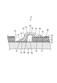
- the circuit assembly 1 shown in FIG. 8 includes a bus bar configuration plate 3 having a plurality of bus bars 2 and a control circuit board 4 bonded to the upper surface of the bus bar configuration plate 3.
- the control circuit board 4 is provided with a substantially rectangular through hole 5, and the upper surface 6 of the bus bar 2 is exposed by the through hole 5.
- conductor pad 7 is provided on control circuit board 4, and conductor pad 7 is located above upper surface 6 of bus bar 2.
- paste-like solder 8 is applied to the upper surface 6 of the bus bar 2
- paste-like solder 8 is also applied to the conductor pads 7, and crank-like terminals 9 are formed on these solders 8.
- the circuit assembly 1 shown in FIG. 8 is obtained by passing it through a reflow furnace in a state in which is placed.
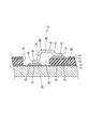
- a defective product shown in FIG. 10 may occur after passing through a reflow furnace.
- the solder 8 is melted in the reflow furnace, the melted solder 8 is transferred to the conductor pad 7 side along the terminal 9 and simultaneously melted with the solder 8 It can be considered that the terminal 9 is attracted to the conductor pad 7 by the surface tension of Therefore, a state where the upper surface 6 of the bus bar 2 and the conductor pad 7 are not connected by the terminal 9, that is, a conduction failure occurs.
- a circuit assembly disclosed by the present specification includes: a circuit board on which a wiring portion is formed; a conductor adhered to one surface of the circuit board; the wiring portion of the circuit board; and the conductor And a terminal for electrically connecting, the terminal having a relay connection between the connection with the wiring portion and the connection with the conductor, the relay connection including the relay connection.
- the other surface of the circuit board protrudes beyond the wiring portion.
- the terminal disclosed by the present specification is a terminal for electrically connecting a wiring portion formed on a circuit board and a conductor adhered to one surface of the circuit board, and A relay connection portion may be provided between the connection portion and the connection portion with the conductor, and the relay connection portion may protrude from the wiring portion on the other surface of the circuit board.
- the solder in the form of paste is applied to the conductor and the wiring portion, and the connection portion between the conductor and the wiring portion is placed on each solder and passed through the reflow furnace
- the connection portion with the conductor is soldered to the conductor
- the connection portion with the wiring portion is soldered to the wiring portion
- the conductor and the wiring portion of the circuit board are electrically connected via the terminals.
- the circuit structure disclosed by the present specification may have the following configuration.
- the circuit board has a through hole for exposing a terminal connection portion provided in the conductor in a state of being bonded to the conductor, and a connection portion with the conductor is provided in the through hole.
- the solder is formed in the shape of a fillet from the copper conductor exposed at the end of the terminal to the surface of the terminal connection portion. According to such a configuration, it can be confirmed that the terminal is soldered properly to the terminal connection portion of the conductor by the fact that the fillet-like solder is formed inside the through hole.
- the relay connection portion of the terminal is provided to extend downward toward the connection portion between the first connection portion provided in a form extending upward from the connection portion with the conductor and the wiring portion, and And a second connecting portion shorter than the first connecting portion.
- the relay connection portion of the terminal has a gate shape projecting laterally along the circuit board, and the connection portion with the conductor and the relay connection portion are connected via a step portion.
- the connection portion with the wiring portion and the relay connection portion may be directly connected in a flush manner. According to such a configuration, since the relay connection portion is disposed along the circuit board, the seating posture of the terminal with respect to the circuit board is stabilized. Moreover, since the connection part with the wiring part and the relay connection part are flush with each other, it is possible to avoid the upsizing of the terminal in the vertical direction.
- the solder can be prevented from rising and the terminal can be prevented from being pulled up to the wiring portion of the circuit board and riding up.
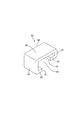
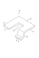
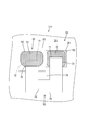
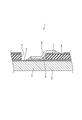
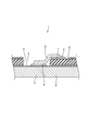
- the perspective view of the terminal in the embodiment 1 Sectional view showing the circuit structure before reflow Sectional view showing a circuit structure after reflow Plan view showing the circuit structure after reflow
- the perspective view of the terminal in Embodiment 2 The perspective view of the terminal in Embodiment 3 Plan view showing the circuit structure after reflow
- Cross-sectional view showing a circuit structure after reflow in the prior art A cross-sectional view showing a circuit structure before reflow in the prior art
- the circuit structure 10 of the present embodiment is configured to include a conductive plate 30, a circuit board 20 bonded to the upper surface of the conductive plate 30, and a terminal 40.
- the conductive plate 30 is formed by punching a conductive metal plate as a base material into a predetermined shape, and a plating layer 31 such as nickel plating is formed on the upper surface of the conductive plate 30.
- the circuit board 20 is fixed to the upper surface of the plating layer 31 via the adhesive 21.
- the conductive plate 30 is a bus bar that constitutes a power circuit mounted on an automobile or the like.
- the circuit board 20 is a control circuit board incorporating a control circuit for controlling the electric power supplied to the conductive plate 30.
- the circuit board 20 is made of a synthetic resin base 22 and a circuit pattern 23 formed on the upper surface of the base 22. And an insulating film 24 applied to the upper surface of the circuit pattern 23.
- the base material 22 is, for example, a flat plate material such as glass epoxy or polyimide, and has an insulating property.
- the circuit pattern 23 is formed by etching a metal plate material such as copper foil, for example, and has conductivity.
- the insulating film 24 is, for example, a resin film such as a solder resist, and plays a role of repelling the paste-like solder 50 to prevent the solder 50 from adhering to the circuit pattern.
- a through hole 25 is provided in the circuit board 20, and a part of the upper surface of the conductive plate 30 is exposed through the through hole 25.
- the exposed portion is a terminal connection portion 32.
- the wiring portion 26 in which a part of the circuit pattern 23 is exposed by not forming the insulating film 24 is provided at a position adjacent to the through hole 25 in the circuit board 20, the wiring portion 26 in which a part of the circuit pattern 23 is exposed by not forming the insulating film 24 is provided.
- the wiring portion 26 is located above the terminal connection portion 32.
- the wiring portion 26 is positioned above the terminal connection portion 32 by the total thickness of the adhesive 21, the base material 22, and the circuit pattern 23.
- the terminal connection portion 32 and the wiring portion 26 are provided side by side in the horizontal direction, and the terminal connection portion 32 is larger than the wiring portion 26.
- the terminal connection portion 32 and the wiring portion 26 are electrically connected by the terminal 40.
- the terminal 40 is obtained by applying a tin plating, a nickel plating, or the like to a copper wire, cutting it at a predetermined length, and bending it. Therefore, copper conductors are exposed at both ends 41 of the terminal 40.
- the terminal 40 is, as shown in FIG. 3, a conductive plate connecting portion 42 soldered to the terminal connecting portion 32, a circuit board connecting portion 43 soldered to the wiring portion 26, a conductive plate connecting portion 42 and a circuit board And a relay connection unit 44 for relay connection of the connection unit 43.
- One end portion 41 of each of the terminals 40 is disposed in each of the conductive plate connecting portion 42 and the circuit board connecting portion 43.
- the relay connection portion 44 includes a first connection portion 45 provided in a form extending upward from the conductive plate connection portion 42, and a detour portion 46 provided in a form extending horizontally from the extending end of the first connection portion 45.
- the second connecting portion 47 is configured to extend downward from the extension end of the bypass portion 46 toward the circuit board connecting portion 43.
- the bypass portion 46 is located above the circuit board connection portion 43, and the second connection portion 47 is shorter than the first connection portion 45. As a result, a space 48 which cuts off the flow of the melted solder 50 is formed between the bypass portion 46 and the terminal connection portion 32.
- solder paste printing step paste solder 50 is applied to the terminal connection portion 32 and the wiring portion 26 respectively, and in the subsequent component mounting step, the solder 50 is applied on each solder 50.
- the terminal 40 is to be placed on the Next, in the reflow process, the solder 50 is melted by passing the circuit assembly 10 on which the terminal 40 is placed in a reflow furnace, and the solder 50 is wetted and spread on each of the terminal connection portion 32 and the wiring portion 26. At this time, although part of the solder 50 wets and spreads from the terminal connection portion 32 to the wiring portion 26 along the terminal 40, all the solder 50 on the terminal connection portion 32 is not wetly spread to the wiring portion 26. ing.
- a space 48 is still formed below the bypass portion 46.
- the height position of the bypass portion 46 is determined by the amount of the volume of the space 48 formed below the bypass portion 46 being the sum of the amount of the solder 50 of the terminal connection portion 32 and the amount of the solder 50 of the wiring portion 26. It is desirable to make the As described above, since the space 48 is not filled with the solder 50, it is assumed that the solder 50 can not rise from the terminal connection portion 32 toward the wiring portion 26.
- a fillet-shaped foot portion 51 is formed in the terminal connection portion 32 by the wetting and spreading of the solder 50. This is because the copper conductor is exposed at both ends 41 of the terminal 40. Since the foot portion 51 is widely spread in the terminal connection portion 32 as shown in FIG. 4, it can be easily confirmed that the soldering is properly performed. Further, although not as wide as the terminal connection portion 32, since the wide bottom portion 51 is formed also in the wiring portion 26, it is easy to confirm that the soldering is properly performed. In addition, since the terminal 40 of the present embodiment has a longer overall length than the structure without the relay connection portion 44 like the terminal 9 shown in FIG. 8, the stress applied to the terminal 40 can be significantly reduced.
- the paste-like solder 50 is applied to the conductor (the conductive plate 30) and the wiring portion 26, and the connection portion with the conductor (the conductive plate connection portion 42) By passing it through a reflow furnace in a state where it is placed on the connection part with the wiring part (circuit board connection part 43), the connection part with the conductor is soldered to the conductor, and the connection part with the wiring part is the wiring part
- the conductor 26 and the wiring portion 26 of the circuit board 20 are electrically connected to each other via the terminal 40 by soldering.
- the solder 50 melted by the conductor passes through the terminal 40 and tries to rise to the wiring portion 26, the flow of the solder 50 is cut off at the relay connection portion 44, so that the solder 50 is prevented from rising. It is possible to prevent the situation in which the terminal 40 is drawn to the wiring portion 26 and rides on. Therefore, the conductor and the wiring portion 26 of the circuit board 20 are connected by the terminal 40, and the conduction failure can be eliminated.
- the circuit board 20 has a through hole 25 for exposing the terminal connection portion 32 provided in the conductor in a state of being bonded to the conductor, and the end of the conductive plate connection portion 42 is inside the through hole 25.
- the solder 50 is formed in a fillet shape from the copper conductor exposed in the portion 41 to the surface of the terminal connection portion 32. According to such a configuration, it is confirmed that the terminal 40 is soldered properly to the terminal connection portion 32 of the conductive plate 30 by the fact that the fillet-like solder 50 is formed inside the through hole 25 it can.
- the relay connection portion 44 of the terminal 40 is a connection portion (circuit board connection portion) between the wiring portion 26 and the first connection portion 45 provided to extend upward from the connection portion with the conductor (conductive plate connection portion 42) And a second connecting portion 47 shorter than the first connecting portion 45.
- the relay connection portion 44 since the relay connection portion 44 is positioned above the connection portion (circuit board connection portion 43) with the wiring portion, the melted solder 50 is a connection portion with a conductor (conductive plate In order to go from the connection portion 42) to the connection portion (circuit board connection portion 43) with the wiring portion, it is necessary to go over the relay connection portion 44, and it becomes easy to prevent the solder 50 from rising.
- the terminal 60 of the present embodiment includes a conductive plate connecting portion 62, a first connecting portion 65 extending upward from the conductive plate connecting portion 62, and a bypass portion 66 extending in the horizontal direction from the extending end of the first connecting portion 65; A second connection portion 67 extending downward from the extension end of the bypass portion 66 and a circuit board connection portion 63 extending horizontally from the extension end of the second connection portion 67 are configured.
- both ends 41 of the conductive plate connecting portion 42 and the circuit board connecting portion 43 face outward, whereas in the terminal 60 of the present embodiment, the conductive plate connecting portion 62 and the circuit board The difference is that both end portions 61 of the connecting portion 63 are directed inward. Further, in the terminal 40 of the first embodiment, the first connecting portion 45 and the second connecting portion 47 are inclined, whereas in the terminal 60 of the present embodiment, the first connecting portion 65 and the second connecting portion 67 are The difference is that they are disposed at right angles to the bypass portion 46.
- the relay connection portion 64 including the first connection portion 65, the detour portion 66, and the second connection portion 67 is longer than the relay connection portion 44 of the first embodiment, and the space 68 is also larger.
- the solder 50 can be more easily prevented from rising.
- Embodiment 3 Next, a third embodiment will be described with reference to FIGS. 6 and 7.
- the present embodiment is a modification of the shape of the terminal 40 of the first embodiment, and the other configuration is the same. Therefore, the same reference numeral is used for the same configuration, and redundant description is omitted. Do.
- the circuit structure 110 is configured to include the circuit board 20, the conductive plate 30, and the terminals 70.
- the terminal 70 includes a conductive plate connection portion 72, a step portion 75 rising upward from the conductive plate connection portion 72, a relay connection portion 74 horizontally extending in a gate shape from the upper end of the step portion 75, and a relay connection portion 74. And a circuit board connection portion 73 directly connected in a flush manner.
- the relay connection portion 74 does not protrude upward, but protrudes laterally along the upper surface of the circuit board 20.
- a space 78 is formed inside the relay connection portion 74, and the flow of the solder 50 can be cut off by the space 78.
- the end portions 71 of the terminals 70 all face in the same direction, and the bottom portion 51 of the solder 50 of this embodiment is slightly larger than those of the first and second embodiments.
- the relay connection portion 74 of the terminal 70 has a gate shape projecting laterally along the circuit board 20, and the connection portion with the conductor (conductive plate connection portion 72) and the relay connection portion 74
- the relay connection portion 74 is connected to the circuit board 20 because the circuit substrate connection portion 73 and the relay connection portion 74 are directly connected flush with each other while being connected via the step portion 75. Since the terminals 70 are disposed along the same, the seating posture of the terminals 70 with respect to the circuit board 20 is stabilized. Further, since the connection portion (circuit board connection portion 73) with the wiring portion 26 and the relay connection portion 74 are flush with each other, the terminal 70 can be prevented from being enlarged in the vertical direction.
- the art disclosed by the present specification is not limited to the embodiments described above with reference to the drawings and the drawings, and includes, for example, various aspects as follows.
- the relay connection parts 44, 64, 74 having a portal shape are illustrated, the relay connection parts do not have to have a portal shape and may be, for example, an arc-shaped relay connection part.
- terminal connection portion 32 is exposed by providing the through hole 25
- the terminal connection portion may be exposed at the edge portion of the circuit board 20 without providing the through hole 25.
- relay connection parts 44, 64 and 74 which project upward or sideways are illustrated in the above embodiment, they may be relay connection parts which project in an oblique direction.
- Conductive plate (conductor) 32 Terminal connection portion 40, 60, 70: Terminal 41, 61, 71: End portion 42, 62, 72: Conductive plate connection portion (connection portion with a conductor) 43, 63, 73 ... Circuit board connection portion (connection portion with wiring portion) 44, 64, 74 ... relay connection portion 45, 65 ... first connection portion 47, 67 ... second connection portion 50 ... solder 75 ... step portion
Landscapes
- Engineering & Computer Science (AREA)
- Manufacturing & Machinery (AREA)
- Microelectronics & Electronic Packaging (AREA)
- Architecture (AREA)
- Civil Engineering (AREA)
- Structural Engineering (AREA)
- Coupling Device And Connection With Printed Circuit (AREA)
- Connections Effected By Soldering, Adhesion, Or Permanent Deformation (AREA)
- Connection Or Junction Boxes (AREA)
Abstract
A circuit structure (10) disclosed by the present description is provided with: a circuit substrate (20) that is provided with a wiring part (26); a conductor (a conductive plate 30) that is bonded to one surface of the circuit substrate (20); and a terminal (40) that electrically connects the wiring part (26) of the circuit substrate (20) and the conductor with each other. The terminal (40) has a relay connection part (44) between a connection part for the wiring part (26) and a connection part for the conductor; and the terminal (40) is configured such that the relay connection part (44) protrudes beyond the wiring part (26) on the other surface of the circuit substrate (20).
Description
本明細書によって開示される技術は、回路構成体および端子に関する。
The technology disclosed by the present specification relates to a circuit structure and a terminal.
従来、自動車等に搭載される電力回路を構成するバスバーとその制御回路が組み込まれた制御回路基板とを備えた回路構成体として、例えば特開2005-224053号公報(下記特許文献1)に記載のものが知られている。このような回路構成体と同様な構成を有する回路構成体を図8から図10に図示して説明する。図8に示す回路構成体1は、複数のバスバー2を有するバスバー構成板3と、このバスバー構成板3の上面に接着された制御回路基板4とを備えている。制御回路基板4には略矩形状の貫通孔5が設けられ、この貫通孔5によりバスバー2の上面6が露出している。一方、制御回路基板4には導体パッド7が設けられ、この導体パッド7は、バスバー2の上面6よりも上方に位置している。図9に示すように、バスバー2の上面6にはペースト状の半田8が塗布され、導体パッド7にもペースト状の半田8が塗布され、これらの半田8の上にクランク状をなす端子9が載置された状態でリフロー炉に通すことにより、図8に示す回路構成体1が得られる。
Conventionally, as a circuit structure provided with a bus bar constituting a power circuit mounted on an automobile etc. and a control circuit board incorporating the control circuit, it is disclosed, for example, in Japanese Patent Application Laid-Open No. 2005-224053 (patent document 1 below) Are known. A circuit structure having the same configuration as such a circuit structure will be described with reference to FIGS. 8 to 10. The circuit assembly 1 shown in FIG. 8 includes a bus bar configuration plate 3 having a plurality of bus bars 2 and a control circuit board 4 bonded to the upper surface of the bus bar configuration plate 3. The control circuit board 4 is provided with a substantially rectangular through hole 5, and the upper surface 6 of the bus bar 2 is exposed by the through hole 5. On the other hand, conductor pad 7 is provided on control circuit board 4, and conductor pad 7 is located above upper surface 6 of bus bar 2. As shown in FIG. 9, paste-like solder 8 is applied to the upper surface 6 of the bus bar 2, paste-like solder 8 is also applied to the conductor pads 7, and crank-like terminals 9 are formed on these solders 8. The circuit assembly 1 shown in FIG. 8 is obtained by passing it through a reflow furnace in a state in which is placed.
上記の回路構成体1において、リフロー炉に通した後に、図10に示す不良品が発生する場合がある。このような不良品が発生する一因としては、リフロー炉内で半田8が溶融した後、溶融した半田8が端子9を伝って導体パッド7側にはい上がり、これと同時に溶融した半田8との表面張力によって端子9が導体パッド7に引き寄せられて乗り上げることが考えられる。このため、バスバー2の上面6と導体パッド7とが端子9によって接続されない状態、すなわち導通不良が発生してしまう。
In the circuit structure 1 described above, after passing through a reflow furnace, a defective product shown in FIG. 10 may occur. As a cause of generation of such defective products, after the solder 8 is melted in the reflow furnace, the melted solder 8 is transferred to the conductor pad 7 side along the terminal 9 and simultaneously melted with the solder 8 It can be considered that the terminal 9 is attracted to the conductor pad 7 by the surface tension of Therefore, a state where the upper surface 6 of the bus bar 2 and the conductor pad 7 are not connected by the terminal 9, that is, a conduction failure occurs.
本明細書によって開示される回路構成体は、配線部が形成された回路基板と、前記回路基板の一方の面に接着される導電体と、前記回路基板の前記配線部と前記導電体とを電気的に接続する端子と、を備え、前記端子は、前記配線部との接続部と、前記導電体との接続部との間に、中継接続部を有し、前記中継接続部は、前記回路基板の他面において前記配線部よりも突出している構成とした。
A circuit assembly disclosed by the present specification includes: a circuit board on which a wiring portion is formed; a conductor adhered to one surface of the circuit board; the wiring portion of the circuit board; and the conductor And a terminal for electrically connecting, the terminal having a relay connection between the connection with the wiring portion and the connection with the conductor, the relay connection including the relay connection. The other surface of the circuit board protrudes beyond the wiring portion.
また、本明細書によって開示される端子は、回路基板に形成された配線部と前記回路基板の一方の面に接着される導電体とを電気的に接続する端子であって、前記配線部との接続部と、前記導電体との接続部との間に、中継接続部を有し、前記中継接続部は、前記回路基板の他面において前記配線部よりも突出している構成としてもよい。
Further, the terminal disclosed by the present specification is a terminal for electrically connecting a wiring portion formed on a circuit board and a conductor adhered to one surface of the circuit board, and A relay connection portion may be provided between the connection portion and the connection portion with the conductor, and the relay connection portion may protrude from the wiring portion on the other surface of the circuit board.
このような構成によると、導電体と配線部にペースト状の半田を塗布し、各半田の上に導電体との接続部と配線部との接続部とを載置した状態でリフロー炉に通すことにより、導電体との接続部が導電体に半田付けされ、配線部との接続部が配線部に半田付けされ、導電体と回路基板の配線部とが端子を介して導通可能に接続される。ここで、導電体にて溶融した半田が端子を伝って配線部へはい上がろうとした場合、中継接続部において半田の流れが断ち切られるため、半田のはい上がりを防止することができ、端子が配線部に引き寄せられて乗り上げる事態を回避できる。したがって、導電体と回路基板の配線部とが端子によって接続されることになり、導通不良をなくすことができる。
According to such a configuration, the solder in the form of paste is applied to the conductor and the wiring portion, and the connection portion between the conductor and the wiring portion is placed on each solder and passed through the reflow furnace Thus, the connection portion with the conductor is soldered to the conductor, the connection portion with the wiring portion is soldered to the wiring portion, and the conductor and the wiring portion of the circuit board are electrically connected via the terminals. Ru. Here, when the solder melted by the conductor passes through the terminal and tries to move up to the wiring portion, the flow of the solder is cut off at the relay connection portion, so that the solder can be prevented from rising and the terminal It is possible to avoid the situation in which the wiring section is pulled up and riding up. Therefore, the conductor and the wiring portion of the circuit board are connected by the terminal, and the conduction failure can be eliminated.
本明細書によって開示される回路構成体は、以下の構成としてもよい。
前記回路基板は、前記導電体に接着された状態において前記導電体に設けられた端子接続部を露出させる貫通孔を有しており、前記貫通孔の内部には、前記導電体との接続部の端部に露出した銅製の導体から前記端子接続部の表面に亘って半田がフィレット状に形成されている構成とした。
このような構成によると、貫通孔の内部においてフィレット状の半田が形成されていることをもって、端子が導電体の端子接続部に対して正常に半田付けされていることを確認できる。 The circuit structure disclosed by the present specification may have the following configuration.
The circuit board has a through hole for exposing a terminal connection portion provided in the conductor in a state of being bonded to the conductor, and a connection portion with the conductor is provided in the through hole. The solder is formed in the shape of a fillet from the copper conductor exposed at the end of the terminal to the surface of the terminal connection portion.
According to such a configuration, it can be confirmed that the terminal is soldered properly to the terminal connection portion of the conductor by the fact that the fillet-like solder is formed inside the through hole.
前記端子の前記中継接続部は、前記導電体との接続部から上方に延びる形態で設けられた第1連結部と、前記配線部との接続部に向けて下方に延びる形態で設けられ、かつ、前記第1連結部よりも短い第2連結部とを備えている構成とした。
このような構成によると、配線部との接続部よりも上方に中継接続部が位置することになるから、溶融した半田が導電体との接続部から配線部との接続部に向かうためには中継接続部を乗り越えていく必要があり、半田のはい上がりを防止しやすくなる。 The relay connection portion of the terminal is provided to extend downward toward the connection portion between the first connection portion provided in a form extending upward from the connection portion with the conductor and the wiring portion, and And a second connecting portion shorter than the first connecting portion.
According to such a configuration, since the relay connection portion is positioned above the connection portion with the wiring portion, the molten solder is directed from the connection portion with the conductor to the connection portion with the wiring portion. It is necessary to get over the relay connection, which makes it easier to prevent the solder from rising.
前記端子の前記中継接続部は、前記回路基板に沿って側方に突出した門形をなし、前記導電体との接続部と前記中継接続部とは、段差部を介して連結されている一方、前記配線部との接続部と前記中継接続部とは、面一をなして直結されている構成としてもよい。
このような構成によると、中継接続部が回路基板に沿って配されるため、端子の回路基板に対する着座姿勢が安定する。また、配線部との接続部と中継接続部とが面一をなしているため、端子が上下方向に大型化することを回避できる。 The relay connection portion of the terminal has a gate shape projecting laterally along the circuit board, and the connection portion with the conductor and the relay connection portion are connected via a step portion. The connection portion with the wiring portion and the relay connection portion may be directly connected in a flush manner.
According to such a configuration, since the relay connection portion is disposed along the circuit board, the seating posture of the terminal with respect to the circuit board is stabilized. Moreover, since the connection part with the wiring part and the relay connection part are flush with each other, it is possible to avoid the upsizing of the terminal in the vertical direction.
本明細書によって開示される回路構成体によれば、半田のはい上がりを防止することができ、端子が回路基板の配線部に引き寄せられて乗り上げる事態を回避できる。
According to the circuit assembly disclosed by the present specification, the solder can be prevented from rising and the terminal can be prevented from being pulled up to the wiring portion of the circuit board and riding up.
<実施形態1>
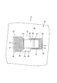
実施形態1を図1から図4の図面を参照しながら説明する。本実施形態の回路構成体10は、図3に示すように、導電板30と、導電板30の上面に接着された回路基板20と、端子40とを備えて構成されている。導電板30は、導電性の金属板を母材として所定の形状に打ち抜くことで形成され、導電板30の上面には例えばニッケルめっきなどのめっき層31が形成されている。このめっき層31の上面に接着材21を介して回路基板20が固定されている。導電板30は自動車等に搭載される電力回路を構成するバスバーである。 First Embodiment
The first embodiment will be described with reference to the drawings of FIGS. 1 to 4. As shown in FIG. 3, thecircuit structure 10 of the present embodiment is configured to include a conductive plate 30, a circuit board 20 bonded to the upper surface of the conductive plate 30, and a terminal 40. The conductive plate 30 is formed by punching a conductive metal plate as a base material into a predetermined shape, and a plating layer 31 such as nickel plating is formed on the upper surface of the conductive plate 30. The circuit board 20 is fixed to the upper surface of the plating layer 31 via the adhesive 21. The conductive plate 30 is a bus bar that constitutes a power circuit mounted on an automobile or the like.
実施形態1を図1から図4の図面を参照しながら説明する。本実施形態の回路構成体10は、図3に示すように、導電板30と、導電板30の上面に接着された回路基板20と、端子40とを備えて構成されている。導電板30は、導電性の金属板を母材として所定の形状に打ち抜くことで形成され、導電板30の上面には例えばニッケルめっきなどのめっき層31が形成されている。このめっき層31の上面に接着材21を介して回路基板20が固定されている。導電板30は自動車等に搭載される電力回路を構成するバスバーである。 First Embodiment
The first embodiment will be described with reference to the drawings of FIGS. 1 to 4. As shown in FIG. 3, the
回路基板20は導電板30に通電される電力を制御する制御回路が組み込まれた制御回路基板であって、合成樹脂製の基材22と、基材22の上面に形成された回路パターン23と、回路パターン23の上面に塗布された絶縁膜24とを備えて構成されている。基材22は、例えばガラスエポキシやポリイミドなどの平板材とされ、絶縁性を有している。回路パターン23は、例えば銅箔などの金属板材をエッチングしたものとされ、導電性を有している。絶縁膜24は、例えばソルダーレジストなどの樹脂被膜とされ、ペースト状の半田50をはじいて回路パターンに半田50が付着することを防止する役割を果たすものである。
The circuit board 20 is a control circuit board incorporating a control circuit for controlling the electric power supplied to the conductive plate 30. The circuit board 20 is made of a synthetic resin base 22 and a circuit pattern 23 formed on the upper surface of the base 22. And an insulating film 24 applied to the upper surface of the circuit pattern 23. The base material 22 is, for example, a flat plate material such as glass epoxy or polyimide, and has an insulating property. The circuit pattern 23 is formed by etching a metal plate material such as copper foil, for example, and has conductivity. The insulating film 24 is, for example, a resin film such as a solder resist, and plays a role of repelling the paste-like solder 50 to prevent the solder 50 from adhering to the circuit pattern.
回路基板20には貫通孔25が設けられており、この貫通孔25を通して導電板30の上面の一部が露出している。この露出した部分は端子接続部32とされている。一方、回路基板20における貫通孔25に隣り合う位置には、絶縁膜24を形成しないことで回路パターン23の一部が露出した配線部26が設けられている。配線部26は端子接続部32よりも上方に位置している。詳細には配線部26は、接着材21と基材22と回路パターン23の合計厚みの分だけ端子接続部32よりも上方に位置している。図4に示すように、端子接続部32と配線部26は水平方向に並んで設けられ、端子接続部32が配線部26よりも大きめとされている。
A through hole 25 is provided in the circuit board 20, and a part of the upper surface of the conductive plate 30 is exposed through the through hole 25. The exposed portion is a terminal connection portion 32. On the other hand, at a position adjacent to the through hole 25 in the circuit board 20, the wiring portion 26 in which a part of the circuit pattern 23 is exposed by not forming the insulating film 24 is provided. The wiring portion 26 is located above the terminal connection portion 32. Specifically, the wiring portion 26 is positioned above the terminal connection portion 32 by the total thickness of the adhesive 21, the base material 22, and the circuit pattern 23. As shown in FIG. 4, the terminal connection portion 32 and the wiring portion 26 are provided side by side in the horizontal direction, and the terminal connection portion 32 is larger than the wiring portion 26.
さて、端子接続部32と配線部26は、端子40によって導通可能に接続されている。端子40は、銅製の線材にすずめっき及びニッケルめっき等を施した後に、所定の長さで切断して曲げ加工を施したものである。このため、端子40の両端部41には、銅製の導体が露出している。端子40は、図3に示すように、端子接続部32に半田付けされる導電板接続部42と、配線部26に半田付けされる回路基板接続部43と、導電板接続部42と回路基板接続部43を中継接続する中継接続部44とを備えて構成されている。端子40の両端部41は、導電板接続部42と回路基板接続部43にそれぞれ1つずつ配設されている。
The terminal connection portion 32 and the wiring portion 26 are electrically connected by the terminal 40. The terminal 40 is obtained by applying a tin plating, a nickel plating, or the like to a copper wire, cutting it at a predetermined length, and bending it. Therefore, copper conductors are exposed at both ends 41 of the terminal 40. The terminal 40 is, as shown in FIG. 3, a conductive plate connecting portion 42 soldered to the terminal connecting portion 32, a circuit board connecting portion 43 soldered to the wiring portion 26, a conductive plate connecting portion 42 and a circuit board And a relay connection unit 44 for relay connection of the connection unit 43. One end portion 41 of each of the terminals 40 is disposed in each of the conductive plate connecting portion 42 and the circuit board connecting portion 43.
中継接続部44は、導電板接続部42から上方に延びる形態で設けられた第1連結部45と、第1連結部45の延出端から水平方向に延びる形態で設けられた迂回部46と、迂回部46の延出端から回路基板接続部43に向けて下方に延びる形態で設けられた第2連結部47とを備えて構成されている。迂回部46は、回路基板接続部43よりも上方に位置し、第2連結部47は、第1連結部45よりも短いものとされている。この結果、迂回部46と端子接続部32の間には、溶融した半田50の流れを断ち切る空間48が形成されている。
The relay connection portion 44 includes a first connection portion 45 provided in a form extending upward from the conductive plate connection portion 42, and a detour portion 46 provided in a form extending horizontally from the extending end of the first connection portion 45. The second connecting portion 47 is configured to extend downward from the extension end of the bypass portion 46 toward the circuit board connecting portion 43. The bypass portion 46 is located above the circuit board connection portion 43, and the second connection portion 47 is shorter than the first connection portion 45. As a result, a space 48 which cuts off the flow of the melted solder 50 is formed between the bypass portion 46 and the terminal connection portion 32.
図2に示すように、半田ペーストの印刷工程では端子接続部32と配線部26に、それぞれペースト状の半田50が塗布されるようになっており、その後の部品実装工程では各半田50の上に端子40が載置されるようになっている。次に、リフロー工程では端子40が載置された回路構成体10をリフロー炉に通すことにより半田50が溶融し、端子接続部32と配線部26のそれぞれで半田50が濡れ広がる。このとき、一部の半田50は、端子40を伝って端子接続部32から配線部26に濡れ広がるものの、端子接続部32上の半田50が全て配線部26に濡れ広がることはないものとされている。
As shown in FIG. 2, in the solder paste printing step, paste solder 50 is applied to the terminal connection portion 32 and the wiring portion 26 respectively, and in the subsequent component mounting step, the solder 50 is applied on each solder 50. The terminal 40 is to be placed on the Next, in the reflow process, the solder 50 is melted by passing the circuit assembly 10 on which the terminal 40 is placed in a reflow furnace, and the solder 50 is wetted and spread on each of the terminal connection portion 32 and the wiring portion 26. At this time, although part of the solder 50 wets and spreads from the terminal connection portion 32 to the wiring portion 26 along the terminal 40, all the solder 50 on the terminal connection portion 32 is not wetly spread to the wiring portion 26. ing.
図3に示すように、迂回部46の下方には依然として空間48が形成されている。つまり、端子接続部32に塗布された半田50の量と配線部26に塗布された半田50の量とを合わせても、空間48を埋め尽くす程の半田50の量には至らないように設定されている。したがって、迂回部46の高さ位置は、迂回部46の下方に形成される空間48の容積が、端子接続部32の半田50の量と配線部26の半田50の量とを合わせた量よりも大きくなるようにすることが望ましい。このように空間48が半田50で埋まらないことから、端子接続部32から配線部26に向けて半田50がはい上がる事態は起こり得ないものとされている。
As shown in FIG. 3, a space 48 is still formed below the bypass portion 46. In other words, even if the amount of the solder 50 applied to the terminal connection portion 32 and the amount of the solder 50 applied to the wiring portion 26 are combined, the amount of the solder 50 is not enough to fill the space 48. It is done. Therefore, the height position of the bypass portion 46 is determined by the amount of the volume of the space 48 formed below the bypass portion 46 being the sum of the amount of the solder 50 of the terminal connection portion 32 and the amount of the solder 50 of the wiring portion 26. It is desirable to make the As described above, since the space 48 is not filled with the solder 50, it is assumed that the solder 50 can not rise from the terminal connection portion 32 toward the wiring portion 26.
図3および図4に示すように、端子接続部32には半田50が濡れ広がることでフィレット形状の裾野部分51が形成されている。これは、端子40の両端部41に銅製の導体が露出しているためである。この裾野部分51は、図4に示すように、端子接続部32において広範囲に広がっているため、正常に半田付けされていることを容易に確認できる。また、端子接続部32ほど広範囲ではないものの、配線部26においても広範囲の裾野部分51が形成されているため、正常に半田付けされていることの確認がしやすい。また、本実施形態の端子40は、図8に示す端子9のように中継接続部44を持たない構造よりも全長が長くなっているため、端子40にかかる応力を大幅に減らすことができる。
As shown in FIG. 3 and FIG. 4, a fillet-shaped foot portion 51 is formed in the terminal connection portion 32 by the wetting and spreading of the solder 50. This is because the copper conductor is exposed at both ends 41 of the terminal 40. Since the foot portion 51 is widely spread in the terminal connection portion 32 as shown in FIG. 4, it can be easily confirmed that the soldering is properly performed. Further, although not as wide as the terminal connection portion 32, since the wide bottom portion 51 is formed also in the wiring portion 26, it is easy to confirm that the soldering is properly performed. In addition, since the terminal 40 of the present embodiment has a longer overall length than the structure without the relay connection portion 44 like the terminal 9 shown in FIG. 8, the stress applied to the terminal 40 can be significantly reduced.
以上のように本実施形態では、導電体(導電板30)と配線部26にペースト状の半田50を塗布し、各半田50の上に導電体との接続部(導電板接続部42)と配線部との接続部(回路基板接続部43)とを載置した状態でリフロー炉に通すことにより、導電体との接続部が導電体に半田付けされ、配線部との接続部が配線部26に半田付けされ、導電体と回路基板20の配線部26とが端子40を介して導通可能に接続される。ここで、導電体にて溶融した半田50が端子40を伝って配線部26へはい上がろうとした場合、中継接続部44において半田50の流れが断ち切られるため、半田50のはい上がりを防止することができ、端子40が配線部26に引き寄せられて乗り上げる事態を回避できる。したがって、導電体と回路基板20の配線部26とが端子40によって接続されることになり、導通不良をなくすことができる。
As described above, in the present embodiment, the paste-like solder 50 is applied to the conductor (the conductive plate 30) and the wiring portion 26, and the connection portion with the conductor (the conductive plate connection portion 42) By passing it through a reflow furnace in a state where it is placed on the connection part with the wiring part (circuit board connection part 43), the connection part with the conductor is soldered to the conductor, and the connection part with the wiring part is the wiring part The conductor 26 and the wiring portion 26 of the circuit board 20 are electrically connected to each other via the terminal 40 by soldering. Here, when the solder 50 melted by the conductor passes through the terminal 40 and tries to rise to the wiring portion 26, the flow of the solder 50 is cut off at the relay connection portion 44, so that the solder 50 is prevented from rising. It is possible to prevent the situation in which the terminal 40 is drawn to the wiring portion 26 and rides on. Therefore, the conductor and the wiring portion 26 of the circuit board 20 are connected by the terminal 40, and the conduction failure can be eliminated.
回路基板20は、導電体に接着された状態において導電体に設けられた端子接続部32を露出させる貫通孔25を有しており、貫通孔25の内部には、導電板接続部42の端部41に露出した銅製の導体から端子接続部32の表面に亘って半田50がフィレット状に形成されている構成とした。
このような構成によると、貫通孔25の内部においてフィレット状の半田50が形成されていることをもって、端子40が導電板30の端子接続部32に対して正常に半田付けされていることを確認できる。 Thecircuit board 20 has a through hole 25 for exposing the terminal connection portion 32 provided in the conductor in a state of being bonded to the conductor, and the end of the conductive plate connection portion 42 is inside the through hole 25. The solder 50 is formed in a fillet shape from the copper conductor exposed in the portion 41 to the surface of the terminal connection portion 32.
According to such a configuration, it is confirmed that the terminal 40 is soldered properly to theterminal connection portion 32 of the conductive plate 30 by the fact that the fillet-like solder 50 is formed inside the through hole 25 it can.
このような構成によると、貫通孔25の内部においてフィレット状の半田50が形成されていることをもって、端子40が導電板30の端子接続部32に対して正常に半田付けされていることを確認できる。 The
According to such a configuration, it is confirmed that the terminal 40 is soldered properly to the
端子40の中継接続部44は、導電体との接続部(導電板接続部42)から上方に延びる形態で設けられた第1連結部45と、配線部26との接続部(回路基板接続部43)に向けて下方に延びる形態で設けられ、かつ、第1連結部45よりも短い第2連結部47とを備えている構成とした。
このような構成によると、配線部との接続部(回路基板接続部43)よりも上方に中継接続部44が位置することになるから、溶融した半田50が導電体との接続部(導電板接続部42)から配線部との接続部(回路基板接続部43)に向かうためには中継接続部44を乗り越えていく必要があり、半田50のはい上がりを防止しやすくなる。 Therelay connection portion 44 of the terminal 40 is a connection portion (circuit board connection portion) between the wiring portion 26 and the first connection portion 45 provided to extend upward from the connection portion with the conductor (conductive plate connection portion 42) And a second connecting portion 47 shorter than the first connecting portion 45.
According to such a configuration, since therelay connection portion 44 is positioned above the connection portion (circuit board connection portion 43) with the wiring portion, the melted solder 50 is a connection portion with a conductor (conductive plate In order to go from the connection portion 42) to the connection portion (circuit board connection portion 43) with the wiring portion, it is necessary to go over the relay connection portion 44, and it becomes easy to prevent the solder 50 from rising.
このような構成によると、配線部との接続部(回路基板接続部43)よりも上方に中継接続部44が位置することになるから、溶融した半田50が導電体との接続部(導電板接続部42)から配線部との接続部(回路基板接続部43)に向かうためには中継接続部44を乗り越えていく必要があり、半田50のはい上がりを防止しやすくなる。 The
According to such a configuration, since the
<実施形態2>
次に、実施形態2を図5の図面によって説明する。本実施形態は実施形態1の端子40の形状を変更したものであって、その他の構成は同じである。本実施形態の端子60は、導電板接続部62と、導電板接続部62から上方に延びる第1連結部65と、第1連結部65の延出端から水平方向に延びる迂回部66と、迂回部66の延出端から下方に延びる第2連結部67と、第2連結部67の延出端から水平方向に延びる回路基板接続部63とを備えて構成されている。 Second Embodiment
A second embodiment will now be described with reference to the drawing of FIG. This embodiment changes the shape of the terminal 40 of the first embodiment, and the other configuration is the same. The terminal 60 of the present embodiment includes a conductiveplate connecting portion 62, a first connecting portion 65 extending upward from the conductive plate connecting portion 62, and a bypass portion 66 extending in the horizontal direction from the extending end of the first connecting portion 65; A second connection portion 67 extending downward from the extension end of the bypass portion 66 and a circuit board connection portion 63 extending horizontally from the extension end of the second connection portion 67 are configured.
次に、実施形態2を図5の図面によって説明する。本実施形態は実施形態1の端子40の形状を変更したものであって、その他の構成は同じである。本実施形態の端子60は、導電板接続部62と、導電板接続部62から上方に延びる第1連結部65と、第1連結部65の延出端から水平方向に延びる迂回部66と、迂回部66の延出端から下方に延びる第2連結部67と、第2連結部67の延出端から水平方向に延びる回路基板接続部63とを備えて構成されている。 Second Embodiment
A second embodiment will now be described with reference to the drawing of FIG. This embodiment changes the shape of the terminal 40 of the first embodiment, and the other configuration is the same. The terminal 60 of the present embodiment includes a conductive
実施形態1の端子40では、導電板接続部42と回路基板接続部43との両端部41が外側を向いているのに対して、本実施形態の端子60では導電板接続部62と回路基板接続部63との両端部61が内側を向いている点で相違している。また、実施形態1の端子40では、第1連結部45と第2連結部47が傾斜しているのに対して、本実施形態の端子60では第1連結部65と第2連結部67が迂回部46に対して直角に配されている点で相違している。このような構成によると、第1連結部65と迂回部66と第2連結部67とからなる中継接続部64が、実施形態1の中継接続部44よりも長くなり、空間68も大きくなるため、半田50のはい上がりをより防止しやすくなる。
In the terminal 40 of the first embodiment, both ends 41 of the conductive plate connecting portion 42 and the circuit board connecting portion 43 face outward, whereas in the terminal 60 of the present embodiment, the conductive plate connecting portion 62 and the circuit board The difference is that both end portions 61 of the connecting portion 63 are directed inward. Further, in the terminal 40 of the first embodiment, the first connecting portion 45 and the second connecting portion 47 are inclined, whereas in the terminal 60 of the present embodiment, the first connecting portion 65 and the second connecting portion 67 are The difference is that they are disposed at right angles to the bypass portion 46. According to such a configuration, the relay connection portion 64 including the first connection portion 65, the detour portion 66, and the second connection portion 67 is longer than the relay connection portion 44 of the first embodiment, and the space 68 is also larger. The solder 50 can be more easily prevented from rising.
<実施形態3>
次に、実施形態3を図6および図7の図面によって説明する。本実施形態は実施形態1の端子40の形状を変更したものであって、その他の構成は同じであるため、同じ構成については同一の符号を用いるものとし、重複する説明については省略するものとする。Embodiment 3
Next, a third embodiment will be described with reference to FIGS. 6 and 7. The present embodiment is a modification of the shape of the terminal 40 of the first embodiment, and the other configuration is the same. Therefore, the same reference numeral is used for the same configuration, and redundant description is omitted. Do.
次に、実施形態3を図6および図7の図面によって説明する。本実施形態は実施形態1の端子40の形状を変更したものであって、その他の構成は同じであるため、同じ構成については同一の符号を用いるものとし、重複する説明については省略するものとする。
Next, a third embodiment will be described with reference to FIGS. 6 and 7. The present embodiment is a modification of the shape of the terminal 40 of the first embodiment, and the other configuration is the same. Therefore, the same reference numeral is used for the same configuration, and redundant description is omitted. Do.
本実施形態の回路構成体110は、回路基板20と、導電板30と、端子70とを備えて構成されている。端子70は、導電板接続部72と、導電板接続部72から上方に立ち上がる段差部75と、段差部75の上端から門形をなして水平方向に延びる中継接続部74と、中継接続部74と面一をなして直結された回路基板接続部73とを備えて構成されている。図7に示すように、中継接続部74は、上方に突出するのではなく、回路基板20の上面に沿って側方に突出する形態とされている。このような構成においても、中継接続部74の内側には、空間78が形成されており、この空間78によって半田50の流れを断ち切ることができる。なお、端子70の両端部71は、いずれも同じ方向を向いており、本実施形態の半田50の裾野部分51は、実施形態1および2よりもやや大きめとされている。
The circuit structure 110 according to the present embodiment is configured to include the circuit board 20, the conductive plate 30, and the terminals 70. The terminal 70 includes a conductive plate connection portion 72, a step portion 75 rising upward from the conductive plate connection portion 72, a relay connection portion 74 horizontally extending in a gate shape from the upper end of the step portion 75, and a relay connection portion 74. And a circuit board connection portion 73 directly connected in a flush manner. As shown in FIG. 7, the relay connection portion 74 does not protrude upward, but protrudes laterally along the upper surface of the circuit board 20. Also in such a configuration, a space 78 is formed inside the relay connection portion 74, and the flow of the solder 50 can be cut off by the space 78. The end portions 71 of the terminals 70 all face in the same direction, and the bottom portion 51 of the solder 50 of this embodiment is slightly larger than those of the first and second embodiments.
すなわち、本実施形態では、端子70の中継接続部74は、回路基板20に沿って側方に突出した門形をなし、導電体との接続部(導電板接続部72)と中継接続部74とは、段差部75を介して連結されている一方、回路基板接続部73と中継接続部74は、面一をなして直結されている構成としたから、中継接続部74が回路基板20に沿って配されるため、端子70の回路基板20に対する着座姿勢が安定する。また、配線部26との接続部(回路基板接続部73)と中継接続部74とが面一をなしているため、端子70が上下方向に大型化することを回避できる。
That is, in the present embodiment, the relay connection portion 74 of the terminal 70 has a gate shape projecting laterally along the circuit board 20, and the connection portion with the conductor (conductive plate connection portion 72) and the relay connection portion 74 The relay connection portion 74 is connected to the circuit board 20 because the circuit substrate connection portion 73 and the relay connection portion 74 are directly connected flush with each other while being connected via the step portion 75. Since the terminals 70 are disposed along the same, the seating posture of the terminals 70 with respect to the circuit board 20 is stabilized. Further, since the connection portion (circuit board connection portion 73) with the wiring portion 26 and the relay connection portion 74 are flush with each other, the terminal 70 can be prevented from being enlarged in the vertical direction.
<他の実施形態>
本明細書によって開示される技術は上記記述及び図面によって説明した実施形態に限定されるものではなく、例えば次のような種々の態様も含まれる。
(1)上記実施形態では、門形をなす中継接続部44、64、74を例示しているものの、門形である必要はなく、例えば弧状をなす中継接続部としてもよい。 Other Embodiments
The art disclosed by the present specification is not limited to the embodiments described above with reference to the drawings and the drawings, and includes, for example, various aspects as follows.
(1) In the above embodiment, although the relay connection parts 44, 64, 74 having a portal shape are illustrated, the relay connection parts do not have to have a portal shape and may be, for example, an arc-shaped relay connection part.
本明細書によって開示される技術は上記記述及び図面によって説明した実施形態に限定されるものではなく、例えば次のような種々の態様も含まれる。
(1)上記実施形態では、門形をなす中継接続部44、64、74を例示しているものの、門形である必要はなく、例えば弧状をなす中継接続部としてもよい。 Other Embodiments
The art disclosed by the present specification is not limited to the embodiments described above with reference to the drawings and the drawings, and includes, for example, various aspects as follows.
(1) In the above embodiment, although the
(2)上記実施形態では、貫通孔25を設けることで端子接続部32を露出させているものの、貫通孔25を設けることなく回路基板20のエッジ部分に端子接続部を露出させてもよい。
(2) In the above embodiment, although the terminal connection portion 32 is exposed by providing the through hole 25, the terminal connection portion may be exposed at the edge portion of the circuit board 20 without providing the through hole 25.
(3)上記実施形態では上方もしくは側方に突出する中継接続部44、64、74を例示しているものの、斜め方向に突出する中継接続部としてもよい。
(3) Although the relay connection parts 44, 64 and 74 which project upward or sideways are illustrated in the above embodiment, they may be relay connection parts which project in an oblique direction.
10、110…回路構成体
20…回路基板
25…貫通孔
26…配線部
30…導電板(導電体)
32…端子接続部
40、60、70…端子
41、61、71…端部
42、62、72…導電板接続部(導電体との接続部)
43、63、73…回路基板接続部(配線部との接続部)
44、64、74…中継接続部
45、65…第1接続部
47、67…第2連結部
50…半田
75…段差部 DESCRIPTION OF SYMBOLS 10, 110 ... Circuit structure 20 ... Circuit board 25 ... Through-hole 26 ... Wiring part 30 ... Conductive plate (conductor)
32: Terminal connection portion 40, 60, 70: Terminal 41, 61, 71: End portion 42, 62, 72: Conductive plate connection portion (connection portion with a conductor)
43, 63, 73 ... Circuit board connection portion (connection portion with wiring portion)
44, 64, 74 ... relay connection portion 45, 65 ... first connection portion 47, 67 ... second connection portion 50 ... solder 75 ... step portion
20…回路基板
25…貫通孔
26…配線部
30…導電板(導電体)
32…端子接続部
40、60、70…端子
41、61、71…端部
42、62、72…導電板接続部(導電体との接続部)
43、63、73…回路基板接続部(配線部との接続部)
44、64、74…中継接続部
45、65…第1接続部
47、67…第2連結部
50…半田
75…段差部 DESCRIPTION OF
32:
43, 63, 73 ... Circuit board connection portion (connection portion with wiring portion)
44, 64, 74 ...
Claims (5)
- 配線部が形成された回路基板と、
前記回路基板の一方の面に接着される導電体と、
前記回路基板の前記配線部と前記導電体とを電気的に接続する端子と、を備え、
前記端子は、前記配線部との接続部と、前記導電体との接続部との間に、中継接続部を有し、
前記中継接続部は、前記回路基板の他面において前記配線部よりも突出している回路構成体。 A circuit board on which a wiring portion is formed;
A conductor adhered to one surface of the circuit board;
A terminal for electrically connecting the wiring portion of the circuit board and the conductor;
The terminal has a relay connection portion between a connection portion with the wiring portion and a connection portion with the conductor,
The circuit configuration body in which the relay connection portion protrudes beyond the wiring portion on the other surface of the circuit board. - 前記回路基板は、前記導電体に接着された状態において前記導電体に設けられた端子接続部を露出させる貫通孔を有しており、前記貫通孔の内部には、前記導電体との接続部の端部に露出した銅製の導体から前記端子接続部の表面に亘って半田がフィレット状に形成されている請求項1に記載の回路構成体。 The circuit board has a through hole for exposing a terminal connection portion provided in the conductor in a state of being bonded to the conductor, and a connection portion with the conductor is provided in the through hole. The circuit structure according to claim 1, wherein the solder is formed in a fillet shape from the copper conductor exposed at the end of the terminal to the surface of the terminal connection portion.
- 前記端子の前記中継接続部は、前記導電体との接続部から上方に延びる形態で設けられた第1連結部と、前記配線部との接続部に向けて下方に延びる形態で設けられ、かつ、前記第1連結部よりも短い第2連結部とを備えている請求項1または請求項2に記載の回路構成体。 The relay connection portion of the terminal is provided to extend downward toward the connection portion between the first connection portion provided in a form extending upward from the connection portion with the conductor and the wiring portion, and The circuit structure according to claim 1, further comprising: a second connection portion shorter than the first connection portion.
- 前記端子の前記中継接続部は、前記回路基板に沿って側方に突出した門形をなし、前記導電体との接続部と前記中継接続部とは、段差部を介して連結されている一方、前記配線部との接続部と前記中継接続部とは、面一をなして直結されている請求項1または請求項2に記載の回路構成体。 The relay connection portion of the terminal has a gate shape projecting laterally along the circuit board, and the connection portion with the conductor and the relay connection portion are connected via a step portion. The circuit assembly according to claim 1, wherein the connection portion with the wiring portion and the relay connection portion are directly connected in a flush manner.
- 回路基板に形成された配線部と前記回路基板の一方の面に接着される導電体とを電気的に接続する端子であって、
前記配線部との接続部と、前記導電体との接続部との間に、中継接続部を有し、
前記中継接続部は、前記回路基板の他面において前記配線部よりも突出している端子。 A terminal for electrically connecting a wiring portion formed on a circuit board and a conductor adhered to one surface of the circuit board,
A relay connection portion is provided between the connection portion with the wiring portion and the connection portion with the conductor,
The relay connection portion is a terminal protruding from the wiring portion on the other surface of the circuit board.
Priority Applications (3)
| Application Number | Priority Date | Filing Date | Title |
|---|---|---|---|
| CN201680049941.1A CN107925172B (en) | 2015-09-08 | 2016-08-18 | Circuit structure and terminal |
| DE112016004059.8T DE112016004059B4 (en) | 2015-09-08 | 2016-08-18 | Circuit arrangement and contact piece |
| US15/754,762 US10347995B2 (en) | 2015-09-08 | 2016-08-18 | Circuit structure and terminal |
Applications Claiming Priority (2)
| Application Number | Priority Date | Filing Date | Title |
|---|---|---|---|
| JP2015176301A JP6540398B2 (en) | 2015-09-08 | 2015-09-08 | Circuit structure |
| JP2015-176301 | 2015-09-08 |
Publications (1)
| Publication Number | Publication Date |
|---|---|
| WO2017043280A1 true WO2017043280A1 (en) | 2017-03-16 |
Family
ID=58240733
Family Applications (1)
| Application Number | Title | Priority Date | Filing Date |
|---|---|---|---|
| PCT/JP2016/074069 WO2017043280A1 (en) | 2015-09-08 | 2016-08-18 | Circuit structure and terminal |
Country Status (5)
| Country | Link |
|---|---|
| US (1) | US10347995B2 (en) |
| JP (1) | JP6540398B2 (en) |
| CN (1) | CN107925172B (en) |
| DE (1) | DE112016004059B4 (en) |
| WO (1) | WO2017043280A1 (en) |
Citations (2)
| Publication number | Priority date | Publication date | Assignee | Title |
|---|---|---|---|---|
| JPS5652870U (en) * | 1979-09-29 | 1981-05-09 | ||
| JP2005224053A (en) * | 2004-02-06 | 2005-08-18 | Auto Network Gijutsu Kenkyusho:Kk | Circuit constituent |
Family Cites Families (21)
| Publication number | Priority date | Publication date | Assignee | Title |
|---|---|---|---|---|
| US4647126A (en) * | 1985-06-17 | 1987-03-03 | Sperry Corporation | Compliant lead clip |
| JPS6273650A (en) * | 1985-09-27 | 1987-04-04 | Hitachi Ltd | Electrical part |
| JPS63111771U (en) * | 1987-01-09 | 1988-07-18 | ||
| JPH0341417Y2 (en) * | 1987-01-09 | 1991-08-30 | ||
| JPH05327169A (en) * | 1992-05-22 | 1993-12-10 | Denki Kagaku Kogyo Kk | Metal base multilayer circuit board |
| US5910885A (en) * | 1997-12-03 | 1999-06-08 | White Electronic Designs Corporation | Electronic stack module |
| US6468830B1 (en) * | 1998-01-26 | 2002-10-22 | Tessera, Inc. | Compliant semiconductor package with anisotropic conductive material interconnects and methods therefor |
| JP2001168487A (en) * | 1999-12-09 | 2001-06-22 | Koa Corp | Jumper element |
| DE10057460C1 (en) * | 2000-11-20 | 2002-08-08 | Tyco Electronics Amp Gmbh | Holding element with a holding clip, arrangement with a carrier plate and a holding element and arrangement with holding element and carrier strip |
| US6685514B2 (en) * | 2002-04-05 | 2004-02-03 | Larry J. Costa | Folding blade electrical terminal |
| JP4274528B2 (en) * | 2003-04-28 | 2009-06-10 | 協伸工業株式会社 | Tab terminal |
| US6984156B2 (en) * | 2003-09-05 | 2006-01-10 | Power-One Limited | Connector for surface mounting subassemblies vertically on a mother board and assemblies comprising the same |
| TWM266583U (en) * | 2004-07-23 | 2005-06-01 | Hon Hai Prec Ind Co Ltd | Electrical connector contact |
| JP2007141570A (en) * | 2005-11-16 | 2007-06-07 | Tokai Rika Co Ltd | Mounting structure of female connector |
| KR100952322B1 (en) * | 2007-12-17 | 2010-04-09 | 케이. 에이. 이 (주) | A receptacle connector for a battery in the mobile electric device |
| JP5119005B2 (en) * | 2008-03-04 | 2013-01-16 | 日本圧着端子製造株式会社 | Socket contact |
| JP2010003651A (en) * | 2008-06-23 | 2010-01-07 | Fujitsu Component Ltd | Connector |
| DE112009005194T5 (en) * | 2009-08-31 | 2012-06-28 | Hewlett-Packard Development Company, L.P. | Surface mount technology component connector |
| JP5711542B2 (en) * | 2011-01-13 | 2015-05-07 | 矢崎総業株式会社 | Board connection terminal and circuit board holding structure |
| JP5869282B2 (en) * | 2011-10-03 | 2016-02-24 | タイコエレクトロニクスジャパン合同会社 | Electrical connector |
| JP5887597B2 (en) * | 2012-09-28 | 2016-03-16 | 北川工業株式会社 | Contact member |
-
2015
- 2015-09-08 JP JP2015176301A patent/JP6540398B2/en active Active
-
2016
- 2016-08-18 DE DE112016004059.8T patent/DE112016004059B4/en active Active
- 2016-08-18 WO PCT/JP2016/074069 patent/WO2017043280A1/en active Application Filing
- 2016-08-18 US US15/754,762 patent/US10347995B2/en active Active
- 2016-08-18 CN CN201680049941.1A patent/CN107925172B/en active Active
Patent Citations (2)
| Publication number | Priority date | Publication date | Assignee | Title |
|---|---|---|---|---|
| JPS5652870U (en) * | 1979-09-29 | 1981-05-09 | ||
| JP2005224053A (en) * | 2004-02-06 | 2005-08-18 | Auto Network Gijutsu Kenkyusho:Kk | Circuit constituent |
Also Published As
| Publication number | Publication date |
|---|---|
| CN107925172A (en) | 2018-04-17 |
| US10347995B2 (en) | 2019-07-09 |
| CN107925172B (en) | 2019-11-15 |
| US20180248273A1 (en) | 2018-08-30 |
| DE112016004059T5 (en) | 2018-06-07 |
| JP2017054620A (en) | 2017-03-16 |
| JP6540398B2 (en) | 2019-07-10 |
| DE112016004059B4 (en) | 2023-08-17 |
Similar Documents
| Publication | Publication Date | Title |
|---|---|---|
| KR101594220B1 (en) | Electronic component, electronic apparatus including the same, and manufacturing method of the electronic apparatus | |
| KR101662264B1 (en) | Solderable elastic electric contact terminal | |
| JP4923841B2 (en) | Circuit material accommodated in electrical junction box and in-vehicle electrical junction box accommodating the circuit material | |
| TW200911064A (en) | Connection structure between printed circuit board and electronic component | |
| JP2005095977A (en) | Circuit device | |
| JP4676855B2 (en) | Hybrid integrated circuit device and manufacturing method thereof | |
| KR20110077042A (en) | Method of making printed circuit board assembly | |
| WO2015045768A1 (en) | Circuit assembly | |
| KR101951732B1 (en) | Conductive contactor for substrate surface mount and preparing method for the same | |
| JP6540398B2 (en) | Circuit structure | |
| JP2004200539A (en) | Component-connecting terminal and electronic device | |
| JP6570728B2 (en) | Electronic device and manufacturing method thereof | |
| JP6007413B2 (en) | Wiring board | |
| JP2010034168A (en) | Electronic component soldering method | |
| JP2004235232A (en) | Mounting structure of electronic component | |
| WO2019216234A1 (en) | Leadless package mounted substrate | |
| JP2002026482A (en) | Mounting structure of electronic component | |
| WO2024142884A1 (en) | Electronic device and method for manufacturing electronic device | |
| JP2006066811A (en) | Mask for solder printing, method for mounting component | |
| TR2021012850T (en) | Printed circuit board and electronic device. | |
| WO2020194440A1 (en) | Printed wiring board and electronic device | |
| JP6487315B2 (en) | Electronic control unit | |
| JP5428612B2 (en) | Electronic component mounting structure | |
| JP5857769B2 (en) | Wiring pattern connection structure and manufacturing method thereof | |
| JP6171898B2 (en) | Electronic device and manufacturing method thereof |
Legal Events
| Date | Code | Title | Description |
|---|---|---|---|
| 121 | Ep: the epo has been informed by wipo that ep was designated in this application |
Ref document number: 16844143 Country of ref document: EP Kind code of ref document: A1 |
|
| WWE | Wipo information: entry into national phase |
Ref document number: 15754762 Country of ref document: US |
|
| WWE | Wipo information: entry into national phase |
Ref document number: 112016004059 Country of ref document: DE |
|
| 122 | Ep: pct application non-entry in european phase |
Ref document number: 16844143 Country of ref document: EP Kind code of ref document: A1 |