WO2017033730A1 - 圧脈波センサ及び生体情報測定装置 - Google Patents
圧脈波センサ及び生体情報測定装置 Download PDFInfo
- Publication number
- WO2017033730A1 WO2017033730A1 PCT/JP2016/073325 JP2016073325W WO2017033730A1 WO 2017033730 A1 WO2017033730 A1 WO 2017033730A1 JP 2016073325 W JP2016073325 W JP 2016073325W WO 2017033730 A1 WO2017033730 A1 WO 2017033730A1
- Authority
- WO
- WIPO (PCT)
- Prior art keywords
- pressure
- terminal portion
- pulse wave
- substrate
- pressure pulse
- Prior art date
- Legal status (The legal status is an assumption and is not a legal conclusion. Google has not performed a legal analysis and makes no representation as to the accuracy of the status listed.)
- Ceased
Links
Images


Classifications
-
- A—HUMAN NECESSITIES
- A61—MEDICAL OR VETERINARY SCIENCE; HYGIENE
- A61B—DIAGNOSIS; SURGERY; IDENTIFICATION
- A61B5/00—Measuring for diagnostic purposes; Identification of persons
- A61B5/02—Detecting, measuring or recording for evaluating the cardiovascular system, e.g. pulse, heart rate, blood pressure or blood flow
- A61B5/021—Measuring pressure in heart or blood vessels
- A61B5/02108—Measuring pressure in heart or blood vessels from analysis of pulse wave characteristics
-
- A—HUMAN NECESSITIES
- A61—MEDICAL OR VETERINARY SCIENCE; HYGIENE
- A61B—DIAGNOSIS; SURGERY; IDENTIFICATION
- A61B5/00—Measuring for diagnostic purposes; Identification of persons
- A61B5/02—Detecting, measuring or recording for evaluating the cardiovascular system, e.g. pulse, heart rate, blood pressure or blood flow
- A61B5/021—Measuring pressure in heart or blood vessels
- A61B5/022—Measuring pressure in heart or blood vessels by applying pressure to close blood vessels, e.g. against the skin; Ophthalmodynamometers
- A61B5/02233—Occluders specially adapted therefor
-
- A—HUMAN NECESSITIES
- A61—MEDICAL OR VETERINARY SCIENCE; HYGIENE
- A61B—DIAGNOSIS; SURGERY; IDENTIFICATION
- A61B5/00—Measuring for diagnostic purposes; Identification of persons
- A61B5/68—Arrangements of detecting, measuring or recording means, e.g. sensors, in relation to patient
- A61B5/6801—Arrangements of detecting, measuring or recording means, e.g. sensors, in relation to patient specially adapted to be attached to or worn on the body surface
- A61B5/6802—Sensor mounted on worn items
- A61B5/681—Wristwatch-type devices
-
- G—PHYSICS
- G01—MEASURING; TESTING
- G01L—MEASURING FORCE, STRESS, TORQUE, WORK, MECHANICAL POWER, MECHANICAL EFFICIENCY, OR FLUID PRESSURE
- G01L9/00—Measuring steady of quasi-steady pressure of fluid or fluent solid material by electric or magnetic pressure-sensitive elements; Transmitting or indicating the displacement of mechanical pressure-sensitive elements, used to measure the steady or quasi-steady pressure of a fluid or fluent solid material, by electric or magnetic means
- G01L9/0041—Transmitting or indicating the displacement of flexible diaphragms
- G01L9/0042—Constructional details associated with semiconductive diaphragm sensors, e.g. etching, or constructional details of non-semiconductive diaphragms
-
- G—PHYSICS
- G01—MEASURING; TESTING
- G01L—MEASURING FORCE, STRESS, TORQUE, WORK, MECHANICAL POWER, MECHANICAL EFFICIENCY, OR FLUID PRESSURE
- G01L9/00—Measuring steady of quasi-steady pressure of fluid or fluent solid material by electric or magnetic pressure-sensitive elements; Transmitting or indicating the displacement of mechanical pressure-sensitive elements, used to measure the steady or quasi-steady pressure of a fluid or fluent solid material, by electric or magnetic means
- G01L9/0041—Transmitting or indicating the displacement of flexible diaphragms
- G01L9/0051—Transmitting or indicating the displacement of flexible diaphragms using variations in ohmic resistance
- G01L9/0052—Transmitting or indicating the displacement of flexible diaphragms using variations in ohmic resistance of piezoresistive elements
- G01L9/0054—Transmitting or indicating the displacement of flexible diaphragms using variations in ohmic resistance of piezoresistive elements integral with a semiconducting diaphragm
-
- A—HUMAN NECESSITIES
- A61—MEDICAL OR VETERINARY SCIENCE; HYGIENE
- A61B—DIAGNOSIS; SURGERY; IDENTIFICATION
- A61B2562/00—Details of sensors; Constructional details of sensor housings or probes; Accessories for sensors
- A61B2562/02—Details of sensors specially adapted for in-vivo measurements
- A61B2562/0247—Pressure sensors
-
- A—HUMAN NECESSITIES
- A61—MEDICAL OR VETERINARY SCIENCE; HYGIENE
- A61B—DIAGNOSIS; SURGERY; IDENTIFICATION
- A61B2562/00—Details of sensors; Constructional details of sensor housings or probes; Accessories for sensors
- A61B2562/02—Details of sensors specially adapted for in-vivo measurements
- A61B2562/028—Microscale sensors, e.g. electromechanical sensors [MEMS]
-
- H—ELECTRICITY
- H01—ELECTRIC ELEMENTS
- H01L—SEMICONDUCTOR DEVICES NOT COVERED BY CLASS H10
- H01L2224/00—Indexing scheme for arrangements for connecting or disconnecting semiconductor or solid-state bodies and methods related thereto as covered by H01L24/00
- H01L2224/01—Means for bonding being attached to, or being formed on, the surface to be connected, e.g. chip-to-package, die-attach, "first-level" interconnects; Manufacturing methods related thereto
- H01L2224/42—Wire connectors; Manufacturing methods related thereto
- H01L2224/47—Structure, shape, material or disposition of the wire connectors after the connecting process
- H01L2224/48—Structure, shape, material or disposition of the wire connectors after the connecting process of an individual wire connector
- H01L2224/4805—Shape
- H01L2224/4809—Loop shape
- H01L2224/48091—Arched
-
- H—ELECTRICITY
- H01—ELECTRIC ELEMENTS
- H01L—SEMICONDUCTOR DEVICES NOT COVERED BY CLASS H10
- H01L2224/00—Indexing scheme for arrangements for connecting or disconnecting semiconductor or solid-state bodies and methods related thereto as covered by H01L24/00
- H01L2224/73—Means for bonding being of different types provided for in two or more of groups H01L2224/10, H01L2224/18, H01L2224/26, H01L2224/34, H01L2224/42, H01L2224/50, H01L2224/63, H01L2224/71
- H01L2224/732—Location after the connecting process
- H01L2224/73251—Location after the connecting process on different surfaces
- H01L2224/73265—Layer and wire connectors
-
- H—ELECTRICITY
- H01—ELECTRIC ELEMENTS
- H01L—SEMICONDUCTOR DEVICES NOT COVERED BY CLASS H10
- H01L2224/00—Indexing scheme for arrangements for connecting or disconnecting semiconductor or solid-state bodies and methods related thereto as covered by H01L24/00
- H01L2224/80—Methods for connecting semiconductor or other solid state bodies using means for bonding being attached to, or being formed on, the surface to be connected
- H01L2224/85—Methods for connecting semiconductor or other solid state bodies using means for bonding being attached to, or being formed on, the surface to be connected using a wire connector
- H01L2224/85909—Post-treatment of the connector or wire bonding area
- H01L2224/8592—Applying permanent coating, e.g. protective coating
-
- H—ELECTRICITY
- H01—ELECTRIC ELEMENTS
- H01L—SEMICONDUCTOR DEVICES NOT COVERED BY CLASS H10
- H01L2924/00—Indexing scheme for arrangements or methods for connecting or disconnecting semiconductor or solid-state bodies as covered by H01L24/00
- H01L2924/10—Details of semiconductor or other solid state devices to be connected
- H01L2924/1015—Shape
- H01L2924/10155—Shape being other than a cuboid
- H01L2924/10158—Shape being other than a cuboid at the passive surface
-
- H—ELECTRICITY
- H01—ELECTRIC ELEMENTS
- H01L—SEMICONDUCTOR DEVICES NOT COVERED BY CLASS H10
- H01L2924/00—Indexing scheme for arrangements or methods for connecting or disconnecting semiconductor or solid-state bodies as covered by H01L24/00
- H01L2924/15—Details of package parts other than the semiconductor or other solid state devices to be connected
- H01L2924/151—Die mounting substrate
- H01L2924/1515—Shape
- H01L2924/15151—Shape the die mounting substrate comprising an aperture, e.g. for underfilling, outgassing, window type wire connections
Definitions
- the present invention relates to a pressure pulse wave sensor and a biological information measuring device.
- a pressure type pressure measuring device that measures a contact pressure with an object to be measured by pressing the object to be measured is known.
- a pulse wave measuring device As a device using this pressure type pressure measuring device, there is a pulse wave measuring device.
- the pulse wave measuring device measures a pressure pulse wave by pressing a substrate having a pressure sensitive element against the body surface in order to measure a pressure pulse wave generated in an artery located relatively shallower than the skin in the living body.
- Measuring the pressure pulse wave of a subject using such a pulse wave measuring device is very important for knowing the health condition of the subject.
- Patent Documents 1 and 2 are documents relating to this type of pressure-type pulse wave measuring device.
- Patent Document 1 describes a pulse wave measuring device that measures a pressure pulse wave using a pressure sensor chip in which pressure-sensitive elements are two-dimensionally arranged.
- Patent Document 2 describes a pulse wave detection device including a pressure sensor chip in which a diaphragm is formed on a flat semiconductor substrate, and an electrical terminal on the surface of the semiconductor substrate and an electrical terminal on a flexible substrate are connected by a brazing material. Has been.
- This diaphragm has a configuration in which a plurality of pressure-sensitive elements are arranged in one direction. From each pressure-sensitive element, a wiring extends toward both sides in an orthogonal direction perpendicular to the one direction, and the end of this wiring is connected to the diaphragm. The flexible substrate is connected.
- Patent Documents 3 and 4 as documents relating to a pressure measuring device for measuring fluid pressure.
- Patent Document 3 describes a catheter in which a tip receiving recess is provided in a catheter body, and the bottom surface of the tip receiving recess is a mounting surface for a pressure sensor chip.
- the diaphragm (strain gauge circuit) of the pressure sensor chip and the wiring portion of the flexible substrate are connected by wire bonding.
- Patent Document 4 describes a pressure detection device that measures an engine intake pressure of an automobile using a pressure sensor chip having a diaphragm mounted on a semiconductor substrate.
- the pressure sensor chip used in the pulse wave measuring device is pressed against the skin in a state where a pressure-sensitive element array in which a plurality of pressure-sensitive elements are arranged in one direction intersects the running direction of the artery.
- the pressure sensor chip is positioned on the artery as described above to determine the optimum pressure-sensitive element and the optimum pressing force, and then based on the signal output from the optimum pressure-sensitive element at the optimum pressing force. A pressure pulse wave is detected.
- each pressure sensitive element in order to determine the optimum pressure sensitive element, each pressure sensitive element can detect the pressure pulse wave under the same conditions. It is required to have the same detection sensitivity.
- the protective member for protecting the wiring connecting the pressure sensor chip and the substrate is deformed by temperature and humidity, the pressure sensor chip may be subjected to compressive stress or tensile stress due to environmental changes. is there.
- each pressure-sensitive element in the pressure-sensitive element array may vary, which causes a problem that it is difficult to accurately detect the pressure pulse wave.
- Patent Document 1 does not disclose a specific configuration of the pressure sensor chip, and the above-described problem cannot be solved.
- wiring extends from each pressure-sensitive element of the pressure-sensitive element array toward both sides in a direction orthogonal to the direction in which the pressure-sensitive element array extends, and at the end of the wiring, A flexible substrate is connected.
- substrate is protected with resin, for example, and when this resin deform
- each pressure sensitive element is almost equally affected by the stress. That is, since there is a low possibility that the detection sensitivity variation of the pressure-sensitive element array is increased, there is no recognition of the above problem.
- Patent Document 3 does not assume the use of a plurality of pressure-sensitive elements or the detection of a pressure pulse wave, and does not recognize the above-described problem.
- Patent Document 4 does not assume that a pressure pulse wave is detected, and does not recognize the above-described problem.
- the present invention has been made in view of the above circumstances, and an object of the present invention is to provide a pressure pulse wave sensor capable of preventing a decrease in detection accuracy of a pressure pulse wave due to a change in use environment, and a biological information measuring device including the pressure pulse wave sensor.
- the pressure pulse wave sensor according to the present invention is arranged at a pressure-sensitive element array composed of a plurality of pressure-sensitive elements arranged in one direction, and an end portion in the one direction of the pressure-sensitive surface on which the pressure-sensitive element array is formed. And a chip-side terminal portion electrically connected to the pressure-sensitive element array, and the pressure-sensitive surface is on the body surface of the living body in a state where the one direction intersects the traveling direction of the artery of the living body A sensor chip used by being pressed; and a substrate having a recess, and the sensor chip is fixed to a bottom surface of the recess, and the chip-side terminal is provided on the surface of the substrate where the recess is formed.
- a board-side terminal for electrically connecting to the board, and further comprising a conductive member that connects the chip-side terminal and the board-side terminal, and a protective member that covers the conductive member. is there.
- the living body information measuring device of the present invention includes the pressure pulse wave sensor and a living body information calculating unit that calculates living body information based on the pressure pulse wave detected by the pressure pulse wave sensor.
- a pressure pulse wave sensor that can prevent a decrease in detection accuracy of a pressure pulse wave due to a change in use environment, and a biological information measuring device including the same.
- FIG. 3 is a schematic sectional view taken along line AA shown in FIG. 2. It is a perspective view which shows the principal part structure which looked at the pressure pulse wave sensor 1 from the side which contacts skin. It is a figure for demonstrating the influence of the stress by the protection member. It is a figure which shows the modification of the perspective view of the pressure pulse wave sensor 1 shown in FIG.
- FIG. 1 is a block diagram showing a configuration of a blood pressure measurement device 100 as a biological information measurement device for explaining an embodiment of the present invention.
- the blood pressure measurement device 100 is, for example, a wrist-worn type that is worn on the wrist.
- the blood pressure measurement device 100 controls the pressure pulse wave sensor 1, a pressure mechanism 2 for pressing the pressure pulse wave sensor 1 against the body surface of the subject, and a signal output from the pressure pulse wave sensor 1. And a control unit 3 that calculates biological information including the blood pressure of the subject based on this signal.
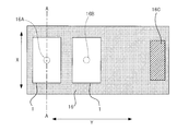
- FIG. 2 is a plan view of the flexible substrate 16 on which the pressure pulse wave sensor 1 shown in FIG. 1 is mounted.
- the flexible substrate 16 has a rectangular shape whose longitudinal direction is a direction Y orthogonal to the direction X, which is one direction, and two pressure pulse wave sensors 1 and a connector 16C are mounted on the surface thereof. .
- the flexible substrate 16 is provided with wiring connected to the electric terminals of the two pressure pulse wave sensors 1 in a resin film. Each wiring is routed to the connector 16C.
- the connector 16C and a connector of a circuit board (not shown) on which the control unit 3 and the like in FIG. 1 are formed are connected.
- the flexible substrate 16 has through holes 16A and 16B substantially in the center of the region where each of the two pressure pulse wave sensors 1 is mounted.
- the through holes 16A and 16B will be described later.
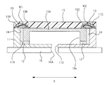
- FIG. 3 is a schematic sectional view taken along line AA shown in FIG.
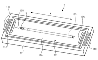
- FIG. 4 is a perspective view showing a main configuration of the pressure pulse wave sensor 1 viewed from the side in contact with the skin. In FIG. 4, illustration of some components is omitted. In FIG. 3, components other than the flexible substrate 16 constitute the pressure pulse wave sensor 1.
- the pressure pulse wave sensor 1 includes a sensor chip 10 and a container-like substrate 11 having a recess 11A and the sensor chip 10 being fixed to the bottom surface of the recess 11A.
- the sensor chip 10 includes a semiconductor substrate 10A such as a silicon single crystal or a single crystal of a compound semiconductor such as gallium-arsenide.
- the semiconductor substrate 10A has a rectangular shape in which the direction X is the longitudinal direction.
- the substrate 11 is composed of a hard substrate having sufficiently higher rigidity than the semiconductor substrate 10A such as a ceramic substrate or a glass substrate.
- the substrate 11 has a rectangular shape in which the direction X is the longitudinal direction.
- the surface of the semiconductor substrate 10 ⁇ / b> A (the surface that comes into contact with the skin of a living body) is composed of a bridge having four strain resistance elements, and a plurality of pressure sensitive elements S for detecting contact pressure. Are arranged along the direction X.
- the plurality of pressure sensitive elements S arranged in the direction X constitute a pressure sensitive element row 10D.
- illustration of the pressure sensitive element S is abbreviate
- the surface opposite to the surface on which the pressure-sensitive element array 10 ⁇ / b> D is formed (hereinafter referred to as pressure-sensitive surface) is perpendicular to the pressure-sensitive surface (hereinafter referred to as sensor pressing direction).
- a recess 10a that is recessed is formed.
- the semiconductor substrate 10A is configured to have a thin portion (diaphragm) whose thickness in the sensor pressing direction is thinner than other portions due to the recess 10a.
- column 10D is formed in the area
- the portion excluding the recess 10a (in other words, the surface where the recess 10a is formed) is fixed to the bottom surface of the recess 11A of the substrate 11 by the adhesive 12.
- the adhesive 12 for example, an ultraviolet curable resin is used.
- the semiconductor substrate 10A is fixed to the bottom surface of the recess 11A of the substrate 11 so that the recess 10a of the semiconductor substrate 10A communicates with the atmosphere only through the through hole 11D formed in the bottom surface of the recess 11A of the substrate 11.
- One pressure pulse wave sensor 1 of the two pressure pulse wave sensors 1 of the blood pressure measurement device 100 is mounted on the flexible substrate 16 so that the through hole 11D and the through hole 16A overlap in a plan view viewed from the pressure-sensitive surface side. Is done.
- the other of the two pressure pulse wave sensors 1 of the blood pressure measurement device 100 is mounted on the flexible substrate 16 so that the through hole 11D and the through hole 16B overlap in the same plan view. .
- the space defined by the semiconductor substrate 10 ⁇ / b> A, the adhesive 12, and the substrate 11 is divided into the through hole 11 ⁇ / b> D of the substrate 11 and the through hole 16 ⁇ / b> A (or the through hole 16 ⁇ / b> B) of the flexible substrate 16. Is maintained at atmospheric pressure (reference pressure).
- the first terminal portion 10B and the second terminal portion 10C that are electrically connected to the pressure-sensitive element array 10D are disposed at both ends in the direction X of the pressure-sensitive surface of the semiconductor substrate 10A.
- the first terminal portion 10B and the second terminal portion 10C are each composed of a plurality of electrode pads arranged in a direction Y orthogonal to the direction X.
- the pressure-sensitive surface of the semiconductor substrate 10A and the surface of the substrate 11 where the recess 11A is formed are based on the bottom surface of the recess 11A of the substrate 11, They are at the same height in the direction perpendicular to the pressure surface. Note that the pressure-sensitive surface of the semiconductor substrate 10A and the surface of the substrate 11 on which the concave portion 11A is formed may not be completely the same height and may include tolerances.
- the fourth terminal portion 11C is provided.
- the third terminal portion 11B, the first terminal portion 10B, the second terminal portion 10C, and the fourth terminal portion 11C are oriented in this order in a plan view as viewed from the direction perpendicular to the pressure-sensitive surface of the semiconductor substrate 10A.
- X is arranged side by side.
- the third terminal portion 11B and the fourth terminal portion 11C are each composed of a plurality of electrode pads arranged in a direction Y orthogonal to the direction X. Each terminal of the third terminal portion 11B corresponds to one of the terminals of the first terminal portion 10B. Each terminal of the fourth terminal portion 11C corresponds to one of the terminals of the second terminal portion 10C.
- each terminal of the first terminal portion 10B and the corresponding terminal of the third terminal portion 11B are electrically connected by a wire W1 that is a first conductive member.
- Each terminal of the second terminal portion 10C and the corresponding terminal of the fourth terminal portion 11C are electrically connected by a wire W2 that is a second conductive member.
- the substrate 11 includes a connection terminal connected to each terminal of the third terminal portion 11B and a connection terminal connected to each terminal of the fourth terminal portion 11C on the flexible substrate 16 side. It is exposed on the surface. These connection terminals are connected to the wiring terminals of the flexible substrate 16.
- the wire W1 and the wire W2 are individually covered and protected by the protective member 13.
- the protective member 13 for example, an epoxy resin or a silicone resin is used.
- the resin material for protecting the wire a material whose volume changes greatly due to environmental conditions such as temperature and humidity is often used.
- the substrate 14 is filled with a material 14 with less volume change due to temperature and humidity than the protective member 13.
- a material 14 for example, a silicone-based resin is used.
- the pressure-sensitive surface of the semiconductor substrate 10A, the protective member 13 of the wire W1, and the protective member 13 of the wire W2 are covered with a surface coating layer 15 for protecting the surface of the pressure pulse wave sensor 1.
- the surface coating layer 15 is made of, for example, a silicone resin.
- the pressure pulse wave sensor 1 configured as described above has the pressure-sensitive element array 10D in a state where the pressure-sensitive element array 10D is located immediately above the artery and the direction X intersects (preferably orthogonally) the running direction of the artery.
- the pressure-sensitive surface of the semiconductor substrate 10A on which 10D is formed is pressed against the body surface of the living body via the surface coating layer 15 and used. Thereby, from each pressure sensitive element S, an electrical signal corresponding to the strain applied to the thin portion of the semiconductor substrate 10A, that is, a signal representing a pressure fluctuation acting on the pressure sensitive element S is output.
- the control unit 3 adjusts the pressing state of the pressure pulse wave sensor 1 on the body surface by the pressing mechanism 2, and based on the signal output from the pressure pulse wave sensor 1, the optimum pressure sensitive element After determining the optimum pressing force, the pressure pulse wave is measured based on the signal output from the optimum pressure-sensitive element at the optimum pressing force, and the biological information such as the blood pressure value and the pulse rate is obtained based on the pressure pulse wave. calculate.
- the height of the pressure-sensitive surface on which the first terminal portion 10B and the second terminal portion 10C are formed with respect to the bottom surface of the recess 11A, and the third terminal The height of the surface of the substrate 11 on which the portion 11B and the fourth terminal portion 11C are formed is substantially the same.
- the length of the wire W1 and the wire W2 can be shortened as compared with the conventional configuration in which the sensor chip 10 is fixed to the flat substrate. As a result, it is possible to reduce the amount of material of the protective member 13 that covers the wires W1, W2.
- the protective member 13 is often made of a material whose volume change increases with changes in temperature and humidity. According to the pressure pulse wave sensor 1, since the amount of this material can be reduced, even if there is a volume change in the protective member 13 depending on the use environment, the influence of the stress on the sensor chip 10 due to the volume change is small. Can be a thing. Therefore, it is possible to prevent a decrease in detection accuracy of the pressure pulse wave due to a change in use environment.
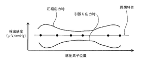
- the pressure pulse wave sensor 1 has a configuration in which the protective member 13 is provided on both ends in the direction X of the pressure-sensitive element array 10D. For this reason, the detection sensitivity of each pressure-sensitive element S in the pressure-sensitive element row 10D is as shown in FIG.
- FIG. 5 shows ideal sensitivity characteristics in which the detection sensitivity of each pressure-sensitive element S is constant, sensitivity characteristics of the pressure-sensitive element array 10D when compressive stress is generated by the protective member 13, and tensile stress by the protective member 13. 4 shows the sensitivity characteristics of the pressure-sensitive element array 10D when the above occurs.
- the pressure-sensitive sensor is located close to the protection member 13 due to the stress generated by the deformation of the protection member 13. It can be seen that the sensitivity varies between the element S and the pressure sensitive element S located far from the protective member 13.
- a wiring protection member is provided on both sides of each pressure-sensitive element in the pressure-sensitive element array.
- each pressure-sensitive element is almost equally affected by the stress generated by the deformation of the wiring protection member. For this reason, even if the volume of the wiring protection member changes greatly, it is possible to keep the detection sensitivity variation of the pressure-sensitive element rows within an allowable range.
- the pressure pulse wave sensor 1 has a configuration in which the protective member 13 is provided on both ends in the direction X of the pressure-sensitive element array 10D. For this reason, as shown in FIG. 5, how the stress is applied to each pressure-sensitive element S greatly varies depending on the position. Therefore, the configuration of the present embodiment that can significantly reduce the volume change of the protection member 13 is very effective.
- the wire and the protective member are not present in the portion that may overlap with the artery, and is flat. For this reason, it becomes easy to transmit a pressure pulse wave to the pressure-sensitive element row
- a material 14 whose volume change due to temperature and humidity is less than that of the protective member 13 is buried between the end face in the direction X of the sensor chip 10 and the substrate 11.
- the material of the protective member 13 does not flow into the gap when the protective member 13 is formed. For this reason, compared with the structure without the material 14, the usage-amount of the material of the protection member 13 can be reduced, and a pressure pulse wave detection accuracy fall can be prevented.
- the sensor chip 10 needs to be fixed to the substrate 11 in order to minimize the gap between the sensor chip 10 and the substrate 11. For this reason, a high accuracy is required for the fixing accuracy of the sensor chip 10 to the substrate 11 and the dimensional accuracy of the sensor chip 10 and the substrate 11, and the manufacturing cost of the pressure pulse wave sensor increases.
- the fixing accuracy and dimensional accuracy described above do not have to be so high, so that an increase in manufacturing cost can be prevented.
- the height of the surface of the substrate 11 on which the terminal portion 11C is formed is assumed to be substantially the same. However, it is not limited to this configuration.
- the height of the pressure-sensitive surface on which the first terminal portion 10B and the second terminal portion 10C are formed with respect to the bottom surface of the concave portion 11A is the third terminal portion 11B and the fourth terminal portion 11C. It may be higher than the height of the surface of the substrate 11 on which is formed.
- the height of the pressure-sensitive surface on which the first terminal portion 10B and the second terminal portion 10C are formed with respect to the bottom surface of the concave portion 11A is the third terminal portion 11B and the fourth terminal portion 11C. It may be lower than the height of the surface of the substrate 11 on which is formed.
- the distance between the sensor chip 10 surface and the substrate surface is about 400 ⁇ m.
- the pressure pulse wave sensor 1 is provided with chip-side terminal portions composed of a first terminal portion 10B and a second terminal portion 10C at both ends in the direction X of the pressure-sensitive surface of the semiconductor substrate 10A, and the first terminal portion 10B. And the board side terminal part comprised by the 3rd terminal part 11B and the 4th terminal part 11C corresponding to each of the 2nd terminal part 10C was set.
- a chip-side terminal portion including terminals electrically connected to each pressure-sensitive element S only at one of both end portions in the direction X of the pressure-sensitive surface of the semiconductor substrate 10 ⁇ / b> A. 10E may be provided.
- each terminal of the chip-side terminal portion 10E is electrically connected to the surface of the substrate 11 where the concave portion 11A is formed on the opposite side of the pressure-sensitive element array 10D in the direction X with respect to the chip-side terminal portion 10E.
- the substrate-side terminal portion 11E made up of terminals for connecting to the substrate may be formed.
- the pressure pulse wave sensor 1 is advantageous for downsizing.
- a wrist-mounted blood pressure measuring device that detects a pressure pulse wave of the radial artery of the wrist has been described, but it may be applied to the carotid artery or the dorsal artery.
- the pressure-sensitive element S for detecting the contact pressure is not limited to the one using the bridge circuit and the diaphragm, but may be another known configuration.
- the blood pressure measurement device 100 has two pressure pulse wave sensors 1. However, if there is at least one pressure pulse wave sensor 1, it is possible to detect the pressure pulse wave and measure biological information. is there.
- the substrate 11 may have a structure in which the side walls at both ends in the direction Y among the side walls of the recess 11A are removed. That is, the substrate 11 may have a substantially U shape.
- the material 14 leaks to the outside in the process of filling the material 14 in the gap between the substrate 11 and the sensor chip 10. No worries. For this reason, the manufacture of the pressure pulse wave sensor 1 can be facilitated.
- connection between each terminal of the first terminal portion 10B and the corresponding terminal of the third terminal portion 11B is not limited to a wire, and may be performed by a conductive member such as a conductive paste.
- connection between each terminal of the second terminal portion 10C and the corresponding terminal of the fourth terminal portion 11C is not limited to a wire, and may be performed by a conductive member such as a conductive paste, for example. Even when any conductive member is used for connection, the protection member 13 for protecting the wiring formed by the conductive member is necessary, and therefore the present invention is effective.
- the pressure pulse wave sensor 1 may be configured such that the material 14 is buried only between the end face of the sensor chip 10 and the substrate 11 in the direction X. If the material 14 is buried in the meantime, when forming the protection member 13, the effect which prevents the volume increase of the protection member 13 by the protection member 13 flowing in during this can be acquired.
- the disclosed pressure pulse wave sensor is arranged at a pressure-sensitive element array composed of a plurality of pressure-sensitive elements arranged in one direction, and an end portion in the one direction of the pressure-sensitive surface on which the pressure-sensitive element array is formed. And a chip-side terminal portion electrically connected to the pressure-sensitive element array, and the pressure-sensitive surface is on the body surface of the living body in a state where the one direction intersects the traveling direction of the artery of the living body
- a board-side terminal for electrically connecting to the board, and further comprising a conductive member that connects the chip-side terminal and the board-side terminal, and a protective member that covers the conductive member. is there.
- the chip-side terminal portion includes a first terminal portion and a second terminal portion that are respectively disposed at both ends of the pressure-sensitive surface in the one direction, and the substrate-side terminal portion. Is constituted by a third terminal portion for electrical connection with the first terminal portion and a fourth terminal portion for electrical connection with the second terminal portion, and the pressure sensitive surface
- the conductive member includes a first conductive member that connects the first terminal portion and the third terminal portion, and a second conductive member that connects the second terminal portion and the fourth terminal portion.
- the protective member includes the first conductive member and the second conductive member, respectively. It is intended to cover separately.
- the disclosed pressure pulse wave sensor has a height of the pressure-sensitive surface on which the chip-side terminal portion is formed and a surface of the substrate on which the substrate-side terminal portion is formed when the bottom surface of the recess is used as a reference.
- the height is the same.
- a material whose volume change due to temperature and humidity is smaller than that of the protective member is buried between the end face of the sensor chip and the substrate in the one direction.
- the disclosed biological information measuring device includes the pressure pulse wave sensor and a biological information calculation unit that calculates biological information based on the pressure pulse wave detected by the pressure pulse wave sensor.
- a pressure pulse wave sensor that can prevent a decrease in detection accuracy of a pressure pulse wave due to a change in use environment, and a biological information measuring device including the pressure pulse wave sensor.
- SYMBOLS 100 Blood pressure measuring device 1 Pressure pulse wave sensor 3 Control part (biological information calculation part) DESCRIPTION OF SYMBOLS 10 Sensor chip S Pressure sensitive element 10A Semiconductor substrate 10B 1st terminal part 10C 2nd terminal part 10D Pressure sensitive element row
Landscapes
- Health & Medical Sciences (AREA)
- Life Sciences & Earth Sciences (AREA)
- Cardiology (AREA)
- Physics & Mathematics (AREA)
- Biomedical Technology (AREA)
- Heart & Thoracic Surgery (AREA)
- Vascular Medicine (AREA)
- Veterinary Medicine (AREA)
- Public Health (AREA)
- Biophysics (AREA)
- Pathology (AREA)
- Engineering & Computer Science (AREA)
- General Health & Medical Sciences (AREA)
- Animal Behavior & Ethology (AREA)
- Medical Informatics (AREA)
- Molecular Biology (AREA)
- Surgery (AREA)
- Physiology (AREA)
- Ophthalmology & Optometry (AREA)
- General Physics & Mathematics (AREA)
- Dentistry (AREA)
- Analytical Chemistry (AREA)
- Chemical & Material Sciences (AREA)
- Measuring Pulse, Heart Rate, Blood Pressure Or Blood Flow (AREA)
Priority Applications (3)
| Application Number | Priority Date | Filing Date | Title |
|---|---|---|---|
| CN201680047186.3A CN108024731B (zh) | 2015-08-24 | 2016-08-08 | 压力脉搏波传感器以及生物体信息测定装置 |
| EP16839077.1A EP3320835B1 (en) | 2015-08-24 | 2016-08-08 | Pressure pulse wave sensor and biological information measurement device |
| US15/893,469 US11344207B2 (en) | 2015-08-24 | 2018-02-09 | Pressure pulse wave sensor and biological information measurement device |
Applications Claiming Priority (2)
| Application Number | Priority Date | Filing Date | Title |
|---|---|---|---|
| JP2015-164697 | 2015-08-24 | ||
| JP2015164697A JP6528602B2 (ja) | 2015-08-24 | 2015-08-24 | 圧脈波センサ及び生体情報測定装置 |
Related Child Applications (1)
| Application Number | Title | Priority Date | Filing Date |
|---|---|---|---|
| US15/893,469 Continuation US11344207B2 (en) | 2015-08-24 | 2018-02-09 | Pressure pulse wave sensor and biological information measurement device |
Publications (1)
| Publication Number | Publication Date |
|---|---|
| WO2017033730A1 true WO2017033730A1 (ja) | 2017-03-02 |
Family
ID=58100118
Family Applications (1)
| Application Number | Title | Priority Date | Filing Date |
|---|---|---|---|
| PCT/JP2016/073325 Ceased WO2017033730A1 (ja) | 2015-08-24 | 2016-08-08 | 圧脈波センサ及び生体情報測定装置 |
Country Status (5)
| Country | Link |
|---|---|
| US (1) | US11344207B2 (enExample) |
| EP (1) | EP3320835B1 (enExample) |
| JP (1) | JP6528602B2 (enExample) |
| CN (1) | CN108024731B (enExample) |
| WO (1) | WO2017033730A1 (enExample) |
Families Citing this family (2)
| Publication number | Priority date | Publication date | Assignee | Title |
|---|---|---|---|---|
| JP7192688B2 (ja) * | 2019-07-16 | 2022-12-20 | Tdk株式会社 | 電子部品パッケージ |
| WO2021106227A1 (ja) * | 2019-11-29 | 2021-06-03 | 村田機械株式会社 | 接圧センサ、それを備えたニット製品、および接圧センサの製造方法 |
Citations (3)
| Publication number | Priority date | Publication date | Assignee | Title |
|---|---|---|---|---|
| JPH0690912A (ja) * | 1992-09-11 | 1994-04-05 | Nippon Colin Co Ltd | 脈波検出装置 |
| JP2004188183A (ja) * | 2002-11-29 | 2004-07-08 | Omron Healthcare Co Ltd | 脈波測定装置 |
| JP2015144628A (ja) * | 2014-01-31 | 2015-08-13 | オムロンヘルスケア株式会社 | 脈波検出装置 |
Family Cites Families (11)
| Publication number | Priority date | Publication date | Assignee | Title |
|---|---|---|---|---|
| JP3039934B2 (ja) * | 1989-06-13 | 2000-05-08 | コーリン電子株式会社 | 圧脈波検出装置 |
| JPH03186247A (ja) * | 1989-12-16 | 1991-08-14 | Koorin Denshi Kk | 脈波検出装置 |
| JP2798764B2 (ja) * | 1990-01-09 | 1998-09-17 | コーリン電子株式会社 | 半導体圧脈波センサ |
| US5179956A (en) * | 1990-07-06 | 1993-01-19 | Colin Electronics Co., Ltd. | Contact pressure sensor |
| US5797850A (en) * | 1993-11-09 | 1998-08-25 | Medwave, Inc. | Method and apparatus for calculating blood pressure of an artery |
| JP3843462B2 (ja) * | 1997-11-20 | 2006-11-08 | セイコーエプソン株式会社 | 脈波診断装置 |
| JP2000287944A (ja) | 1999-04-06 | 2000-10-17 | Tokai Rika Co Ltd | カテーテル用圧力センサブロック |
| JP2004361308A (ja) * | 2003-06-06 | 2004-12-24 | Fuji Electric Device Technology Co Ltd | 物理量検出装置および物理量検出手段格納ケース |
| JP2007301232A (ja) | 2006-05-12 | 2007-11-22 | Omron Healthcare Co Ltd | 圧脈波センサおよびこれを備えた脈波測定装置 |
| JP2008136655A (ja) | 2006-12-01 | 2008-06-19 | Omron Healthcare Co Ltd | 脈波測定用電極ユニットおよび脈波測定装置 |
| CN104540450A (zh) * | 2012-08-09 | 2015-04-22 | 柯尼卡美能达株式会社 | 生物体信息测定装置以及脉搏血氧计 |
-
2015
- 2015-08-24 JP JP2015164697A patent/JP6528602B2/ja active Active
-
2016
- 2016-08-08 EP EP16839077.1A patent/EP3320835B1/en active Active
- 2016-08-08 WO PCT/JP2016/073325 patent/WO2017033730A1/ja not_active Ceased
- 2016-08-08 CN CN201680047186.3A patent/CN108024731B/zh active Active
-
2018
- 2018-02-09 US US15/893,469 patent/US11344207B2/en active Active
Patent Citations (3)
| Publication number | Priority date | Publication date | Assignee | Title |
|---|---|---|---|---|
| JPH0690912A (ja) * | 1992-09-11 | 1994-04-05 | Nippon Colin Co Ltd | 脈波検出装置 |
| JP2004188183A (ja) * | 2002-11-29 | 2004-07-08 | Omron Healthcare Co Ltd | 脈波測定装置 |
| JP2015144628A (ja) * | 2014-01-31 | 2015-08-13 | オムロンヘルスケア株式会社 | 脈波検出装置 |
Non-Patent Citations (1)
| Title |
|---|
| See also references of EP3320835A4 * |
Also Published As
| Publication number | Publication date |
|---|---|
| EP3320835A4 (en) | 2019-02-27 |
| CN108024731B (zh) | 2020-12-15 |
| JP6528602B2 (ja) | 2019-06-12 |
| US20180160919A1 (en) | 2018-06-14 |
| EP3320835A1 (en) | 2018-05-16 |
| EP3320835B1 (en) | 2020-06-24 |
| US11344207B2 (en) | 2022-05-31 |
| JP2017042207A (ja) | 2017-03-02 |
| CN108024731A (zh) | 2018-05-11 |
Similar Documents
| Publication | Publication Date | Title |
|---|---|---|
| US9446944B2 (en) | Sensor apparatus and method for producing a sensor apparatus | |
| CN107445133B (zh) | 对热机械封装应力具有低灵敏度的小型负荷传感器装置 | |
| EP2796830B1 (en) | Strain measuring device | |
| US8516892B2 (en) | Pressure sensor module and electronic component | |
| US20150276517A1 (en) | Mechanical Quantity Measuring Device | |
| EP3453320B1 (en) | Pulse wave detection device and biological information measurement device | |
| US10136858B2 (en) | Method for inspecting pressure pulse wave sensor and method for manufacturing pressure pulse wave sensor | |
| US11344207B2 (en) | Pressure pulse wave sensor and biological information measurement device | |
| EP3660476B1 (en) | Cost overmolded leadframe force sensor with multiple mounting positions | |
| CN107490337B (zh) | 应变检测器及其制造方法 | |
| US20180160918A1 (en) | Pulse wave measurement device | |
| CN107250751B (zh) | 液压传感器、液压控制单元和组件以及车辆制动系统 | |
| KR20150129913A (ko) | 압저항형 세라믹 압력센서 | |
| US20150082898A1 (en) | Strain sensor | |
| JP2010025760A (ja) | 半導体センサ | |
| KR20110059028A (ko) | 반도체 스트레인게이지형 압력센서모듈과 그 제조방법 | |
| JP2006153515A (ja) | 加速度センサ |
Legal Events
| Date | Code | Title | Description |
|---|---|---|---|
| 121 | Ep: the epo has been informed by wipo that ep was designated in this application |
Ref document number: 16839077 Country of ref document: EP Kind code of ref document: A1 |
|
| WWE | Wipo information: entry into national phase |
Ref document number: 2016839077 Country of ref document: EP |
|
| NENP | Non-entry into the national phase |
Ref country code: DE |