WO2017018200A1 - 温度制御装置 - Google Patents
温度制御装置 Download PDFInfo
- Publication number
- WO2017018200A1 WO2017018200A1 PCT/JP2016/070520 JP2016070520W WO2017018200A1 WO 2017018200 A1 WO2017018200 A1 WO 2017018200A1 JP 2016070520 W JP2016070520 W JP 2016070520W WO 2017018200 A1 WO2017018200 A1 WO 2017018200A1
- Authority
- WO
- WIPO (PCT)
- Prior art keywords
- output voltage
- transistor
- peltier element
- unit
- control unit
- Prior art date
- Legal status (The legal status is an assumption and is not a legal conclusion. Google has not performed a legal analysis and makes no representation as to the accuracy of the status listed.)
- Ceased
Links
Images





Classifications
-
- F—MECHANICAL ENGINEERING; LIGHTING; HEATING; WEAPONS; BLASTING
- F25—REFRIGERATION OR COOLING; COMBINED HEATING AND REFRIGERATION SYSTEMS; HEAT PUMP SYSTEMS; MANUFACTURE OR STORAGE OF ICE; LIQUEFACTION SOLIDIFICATION OF GASES
- F25B—REFRIGERATION MACHINES, PLANTS OR SYSTEMS; COMBINED HEATING AND REFRIGERATION SYSTEMS; HEAT PUMP SYSTEMS
- F25B21/00—Machines, plants or systems, using electric or magnetic effects
- F25B21/02—Machines, plants or systems, using electric or magnetic effects using Peltier effect; using Nernst-Ettinghausen effect
-
- G—PHYSICS
- G05—CONTROLLING; REGULATING
- G05D—SYSTEMS FOR CONTROLLING OR REGULATING NON-ELECTRIC VARIABLES
- G05D23/00—Control of temperature
- G05D23/19—Control of temperature characterised by the use of electric means
- G05D23/20—Control of temperature characterised by the use of electric means with sensing elements having variation of electric or magnetic properties with change of temperature
-
- H—ELECTRICITY
- H01—ELECTRIC ELEMENTS
- H01S—DEVICES USING THE PROCESS OF LIGHT AMPLIFICATION BY STIMULATED EMISSION OF RADIATION [LASER] TO AMPLIFY OR GENERATE LIGHT; DEVICES USING STIMULATED EMISSION OF ELECTROMAGNETIC RADIATION IN WAVE RANGES OTHER THAN OPTICAL
- H01S5/00—Semiconductor lasers
- H01S5/02—Structural details or components not essential to laser action
- H01S5/024—Arrangements for thermal management
-
- H—ELECTRICITY
- H10—SEMICONDUCTOR DEVICES; ELECTRIC SOLID-STATE DEVICES NOT OTHERWISE PROVIDED FOR
- H10N—ELECTRIC SOLID-STATE DEVICES NOT OTHERWISE PROVIDED FOR
- H10N10/00—Thermoelectric devices comprising a junction of dissimilar materials, i.e. devices exhibiting Seebeck or Peltier effects
- H10N10/10—Thermoelectric devices comprising a junction of dissimilar materials, i.e. devices exhibiting Seebeck or Peltier effects operating with only the Peltier or Seebeck effects
-
- Y—GENERAL TAGGING OF NEW TECHNOLOGICAL DEVELOPMENTS; GENERAL TAGGING OF CROSS-SECTIONAL TECHNOLOGIES SPANNING OVER SEVERAL SECTIONS OF THE IPC; TECHNICAL SUBJECTS COVERED BY FORMER USPC CROSS-REFERENCE ART COLLECTIONS [XRACs] AND DIGESTS
- Y02—TECHNOLOGIES OR APPLICATIONS FOR MITIGATION OR ADAPTATION AGAINST CLIMATE CHANGE
- Y02B—CLIMATE CHANGE MITIGATION TECHNOLOGIES RELATED TO BUILDINGS, e.g. HOUSING, HOUSE APPLIANCES OR RELATED END-USER APPLICATIONS
- Y02B30/00—Energy efficient heating, ventilation or air conditioning [HVAC]
- Y02B30/70—Efficient control or regulation technologies, e.g. for control of refrigerant flow, motor or heating
Definitions
- This invention relates to the temperature control apparatus which performs temperature control with respect to object apparatus using a Peltier device.
- a Peltier element is a plate-shaped semiconductor element configured by connecting two types of metals or a metal and a semiconductor. When a direct current is passed through a junction between two types of metals, heat is generated from one metal to the other. Moves, and one surface absorbs heat, and the other surface generates heat.
- the Peltier element can control the amount of heat transfer according to the value of current flowing from one surface to the other surface of the Peltier element. Therefore, by disposing the Peltier element on the target device and performing drive control (power supply control) on the Peltier element, high-precision temperature control on the target device can be realized using the Peltier effect. .
- Patent Document 1 describes an invention related to an operation detection circuit for a Peltier element, and the operation detection device switches the direction of a drive current to the Peltier element by an H-bridge circuit to perform an exothermic operation or an endothermic operation.
- the switch unit is configured to switch and input the potential of the Peltier element in the off period of the PWM signal during the endurance or endothermic operation, and to detect the Seebeck voltage of the Peltier element from the input potential in the off period.
- the Seebeck voltage means a voltage generated according to a temperature difference generated between the heat radiation surface and the cooling surface.
- the motion detection device described in Patent Document 1 can detect the Seebeck voltage of the Peltier element during the operation of the Peltier element, and operates the Peltier element by the Seebeck voltage detected by the detection unit while operating the Peltier element.
- the condition (especially the occurrence of thermal runaway) is detected and predicted.
- the drive control of the Peltier element may be stopped.
- the polarity of the Peltier element that is, when the heat dissipation surface and the cooling surface of the Peltier element are switched
- the Peltier element is driven. The case where it transfers to the sleep state which waits for execution of control is mentioned.
- thermoelectric device there may be a temperature difference between one surface and the other surface of the Peltier element, and a Seebeck voltage is generated from the Peltier element, and various components (for example, , A control IC) and the like, which may cause damage and malfunction of the temperature control device and various components.
- various components for example, , A control IC
- the detection unit detects the Seebeck voltage of the Peltier element in the OFF section of the PWM signal, and detects the operating state of the Peltier element (particularly, occurrence of thermal runaway) based on the detected Seebeck voltage. It is an expected configuration and seems to be able to prevent the problems caused by the Seebeck voltage as described above. However, in the case of the invention described in Patent Document 1, a configuration such as a detection unit is required to measure the Seebeck voltage, resulting in a complicated circuit configuration.
- the present disclosure has been made in view of the above-described problems, and relates to a temperature control apparatus that performs temperature control on a target device using a Peltier element, and temperature control capable of preventing a problem caused by a Seebeck voltage generated in the Peltier element. Providing equipment.
- a temperature control device for performing temperature control on a target device, and is provided for the target device, and includes a first terminal and a first terminal.
- a Peltier element having two terminals; a temperature detection unit that detects a temperature related to the target device; and a control signal related to drive control of the Peltier element according to the temperature detected by the temperature detection unit,
- a control unit that performs temperature control on the device, and a first output terminal that is electrically connected to the first terminal of the Peltier element, and based on a control signal from the control unit,
- a first output voltage adjustment unit for adjusting an output voltage to the first terminal; an end portion electrically connected to the first output terminal of the first output voltage adjustment unit; and an electrical connection to a ground potential.
- a second output voltage adjustment unit that adjusts an output voltage to the second terminal of the first output terminal, an end portion that is electrically connected to the second output terminal of the second output voltage adjustment unit, and an electrical connection to a ground potential.
- a second transistor having the other end, and the control unit stops the driving of the first output voltage adjustment unit or the second output voltage adjustment unit. The second transistor is turned on.
- the temperature control device includes a Peltier element, a temperature detection unit, a control unit, a first output voltage adjustment unit, a first transistor, a second output voltage adjustment unit, and a second transistor.
- a Peltier element By controlling the output voltage for the Peltier element, it is possible to perform drive control of the Peltier element and to perform temperature control for the target device.
- the Seebeck effect is generated in the Peltier element, and the Seebeck voltage may be generated.
- the first transistor and the second transistor are made to be conductive.
- the first terminal and the second terminal can be short-circuited. Accordingly, in the temperature control device, the Seebeck voltage generated in the Peltier element is applied to other components (for example, the first output voltage adjustment unit, the second output voltage adjustment unit, etc.) constituting the temperature control device. Therefore, it is possible to prevent problems such as breakage and malfunction of the temperature control device and its components.
- a temperature control device is the temperature control device according to claim 1, wherein the control unit drives the first output voltage adjustment unit to turn off the first transistor.
- the driving of the second output voltage adjusting unit is stopped and the second transistor is turned on, so that the target device is cooled by the Peltier device by cooling the target device and cooling the target device.
- the second output voltage is stopped after stopping the driving of the first output voltage adjusting unit and conducting the first transistor, and after executing the stopping process.
- a heating driving process for driving the Peltier element by heating is performed by driving the adjusting unit and turning off the second transistor.
- the control unit when the Peltier element is driven in the cooling state, the control unit performs the stop process and the heating drive process, thereby reliably switching the Peltier element from the cooling state to the heating state. Drive control can be performed.
- the temperature control device it is possible to short-circuit the first terminal and the second terminal of the Peltier element by executing the stop process in the process of switching from the cooling state to the heating state, and thus according to the Seebeck voltage. Problems such as breakage and malfunction of the temperature control device and its components can be prevented.
- a temperature control device is the temperature control device according to claim 1, wherein the control unit drives the second output voltage adjustment unit to turn off the second transistor.
- the driving of the first output voltage adjusting unit is stopped and the first transistor is turned on, so that the target device is heated by the Peltier device by heating the Peltier device to heat the target device.
- the first output voltage And a cooling drive process for driving the Peltier element to be cooled by driving the adjusting unit and making the first transistor non-conductive.
- the control unit when the Peltier element is driven in the heating state, the control unit performs the stop process and the cooling drive process, thereby reliably switching the Peltier element from the heating state to the cooling state. Drive control can be performed.
- the temperature control device it is possible to short-circuit the first terminal and the second terminal of the Peltier element by executing the stop process in the process of switching from the heating state to the cooling state, and according to the Seebeck voltage. Problems such as breakage and malfunction of the temperature control device and its components can be prevented.
- a temperature control device is the temperature control device according to claim 1, wherein the control unit shifts to a sleep state that waits for execution of drive control of the Peltier element. Executing sleep transition processing for conducting the first transistor and the second transistor when the driving of the first output voltage adjustment unit and the second output voltage adjustment unit is stopped to enter the sleep state.
- the control unit when shifting to a sleep state waiting for execution of the drive control of the Peltier element, the control unit executes the sleep transition process, thereby connecting the first terminal and the second terminal of the Peltier element. Therefore, it is possible to prevent a malfunction such as breakage or malfunction of the temperature control device and its components due to the Seebeck voltage.
- a temperature control device is the temperature control device according to claim 4, wherein the control unit cancels the sleep state and resumes execution of drive control of the Peltier element.
- the control unit cancels the sleep state and resumes execution of drive control of the Peltier element.
- a cooling driving process for driving the Peltier element to cool, and driving the second output voltage adjusting unit is performed by making the second transistor non-conductive.
- the control unit executes either the cooling drive process or the heating drive process. Therefore, even when the sleep state is cancelled, it is possible to appropriately control the temperature of the target device while preventing problems such as breakage or malfunction of the temperature control device and its components due to the Seebeck voltage.
- a temperature control device is the temperature control device according to any one of claims 1 to 5, wherein the control unit is the first output voltage adjustment unit or the second output.
- the control unit is the first output voltage adjustment unit or the second output.
- the first transistor and the second transistor when the first transistor and the second transistor are turned on to stop driving the first output voltage adjustment unit or the second output voltage adjustment unit, the first output After the output voltage output from the voltage adjustment unit or the second output voltage adjustment unit to the Peltier element is minimized, the first transistor and the second transistor are turned on.
- the larger the output voltage output from the first output voltage adjustment unit or the second output voltage adjustment unit the higher the Seebeck voltage of the Peltier element.
- the larger the output voltage output from the first output voltage adjustment unit or the second output voltage adjustment unit the larger the amount of stored charge, and when the first transistor and the second transistor are made conductive, The current flowing into the first transistor and the second transistor increases.
- the first transistor and the second transistor are made conductive. The breakage of the first transistor and the second transistor can be suppressed.
- a temperature control device is the temperature control device according to claim 6, wherein the control unit stops driving the first output voltage adjustment unit or the second output voltage adjustment unit. Therefore, when the first transistor and the second transistor are made conductive, the output voltage output from the first output voltage adjustment unit or the second output voltage adjustment unit to the Peltier element becomes a minimum value. The output voltage is lowered stepwise.
- the first output In order to lower the output voltage stepwise until the output voltage output from the voltage adjustment unit or the second output voltage adjustment unit reaches the minimum value, the temperature difference between the Peltier elements is reliably reduced, and the Seebeck voltage is reduced. Therefore, damage to the first transistor and the second transistor can be suppressed while protecting the components in the temperature control device.
- a temperature control device is the temperature control device according to any one of claims 1 to 7, wherein the first terminal of the Peltier element, the first transistor, and the first transistor are provided.
- the power supply voltage to the temperature control device is disconnected between the output voltage adjusting unit or between the second terminal of the Peltier element and the second transistor and the second output voltage adjusting unit. It has a relay switch which disconnects the electrical connection with respect to the said Peltier device.
- a relay switch is provided between the first terminal of the Peltier element and the first transistor and the first output voltage adjustment unit, or the second terminal of the Peltier element, and the first It is disposed between two transistors and the second output voltage adjustment unit, and disconnects the electrical connection to the Peltier element when the power supply voltage to the temperature control device is cut.
- the temperature control device when the power supply voltage to the temperature control device is cut, drive control of the Peltier element is inevitably stopped, so that a Seebeck voltage can be generated in the Peltier element. Even in this case, since the electrical connection to the Peltier element is disconnected by the relay switch, according to the temperature control device, problems such as breakage or malfunction of the temperature control device and its components due to the Seebeck voltage are caused. Can be prevented.
- the laser processing system 100 includes a laser processing apparatus 1 and a PC 7.
- a pulse is applied to the surface of the workpiece W.
- the laser L is two-dimensionally scanned to perform marking processing.
- the laser processing apparatus 1 includes a laser processing apparatus main body 2, a laser controller 5, and a power supply unit 6.
- the laser processing apparatus main body 2 can perform a marking process on the surface of the processing target by irradiating the processing target with the pulse laser L and scanning the pulse laser L two-dimensionally.
- the laser controller 5 is configured by a computer, is connected to the PC 7 so as to be capable of bidirectional communication, and is electrically connected to the laser processing apparatus main body 2 and the power supply unit 6.
- the PC 7 is composed of a personal computer or the like, and is used for creating machining data.
- the laser controller 5 drives and controls the laser processing apparatus main body 2 and the power supply unit 6 based on the processing data, control parameters, various instruction information, and the like transmitted from the PC 7.
- FIG. 1 shows schematic structure of the laser processing system 100 and the laser processing apparatus 1, the laser processing apparatus main-body part 2 is shown typically. Therefore, a specific configuration of the laser processing apparatus main body 2 will be described later.
- the left direction, the right direction, the upper direction, and the lower direction in FIG. 1 are the front direction, the rear direction, the upper direction, and the lower direction, respectively. Therefore, the emission direction of the pulse laser L of the laser oscillator 21 is the forward direction.
- the direction perpendicular to the main body base 11 and the pulse laser L is the vertical direction.
- the direction orthogonal to the up-down direction and the front-rear direction of the laser processing apparatus main body 2 is the left-right direction of the laser processing apparatus main body 2.
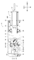
- the laser processing apparatus main body 2 includes a laser head 3 (see FIG. 2) that emits the pulse laser L and the visible laser light M coaxially from the f ⁇ lens 20, and a substantially box body on which the laser head 3 is fixed to the upper surface. And a cylindrical processing container (not shown).
- the laser head unit 3 includes a main body base 11, a laser oscillation unit 12 that emits a pulse laser L, an optical shutter unit 13, an optical damper 14, a half mirror 15, and a guide light unit 16. And a reflection mirror 17, an optical sensor 18, a galvano scanner 19, an f ⁇ lens 20, and the like, and is covered with a substantially rectangular parallelepiped housing cover (not shown).
- the laser oscillation unit 12 includes a laser oscillator 21, a beam expander 22, and a mounting base 23.
- the laser oscillator 21 has a fiber connector, a condenser lens, a reflecting mirror, a laser medium, a passive Q switch, an output coupler, and a window in a casing. Since the laser oscillator 21 generates heat as it is driven to emit the pulse laser L, the laser oscillator 21 is provided with a Peltier element Pb described later. In the laser processing apparatus 1, the laser oscillator 21 is maintained within a predetermined temperature range by performing drive control of the Peltier element Pb using a Peltier driver 50 described later.
- An optical fiber F is connected to the fiber connector, and pumping light emitted from the pumping semiconductor laser unit 40 constituting the power supply unit 6 enters through the optical fiber F.
- the condensing lens condenses the excitation light incident from the fiber connector.
- the reflecting mirror transmits the excitation light collected by the condenser lens and reflects the laser light emitted from the laser medium with high efficiency.
- the laser medium is excited by excitation light emitted from the excitation semiconductor laser unit 40 and oscillates laser light.
- the laser medium include a neodymium-added gadolinium vanadate (Nd: GdVO4) crystal to which neodymium (Nd) is added as a laser active ion, a neodymium-added yttrium vanadate (Nd: YVO4) crystal, and a neodymium-added yttrium aluminum garnet. (Nd: YAG) crystal or the like can be used.
- the passive Q switch is a crystal having a property that the transmittance increases when the light energy stored inside exceeds a certain value. Therefore, the passive Q switch functions as a Q switch that oscillates the laser light oscillated by the laser medium as a pulsed pulse laser.
- a chrome-added YAG (Cr: YAG) crystal, Cr: MgSiO4 crystal, or the like can be used as the passive Q switch.
- the output coupler constitutes a reflecting mirror and a laser resonator.
- the output coupler is, for example, a partial reflecting mirror constituted by a concave mirror whose surface is coated with a dielectric layer film, and the reflectance at a wavelength of 1064 nm is 80% to 95%.
- the window is made of synthetic quartz or the like, and transmits the laser light emitted from the output coupler to the outside. Accordingly, the laser oscillator 21 oscillates a pulse laser through the passive Q switch, and outputs a pulse laser as the pulse laser L for processing the workpiece.
- the beam expander 22 changes the beam diameter of the pulse laser L and is provided coaxially with the laser oscillator 21.
- the mounting base 23 is attached so that the laser oscillator 21 can adjust the optical axis of the pulse laser L, and is fixed to the upper surface on the rear side of the main body base 11 in the front-rear direction by a mounting screw 25.
- the optical shutter unit 13 includes a shutter motor 26 and a flat shutter 27.
- the shutter motor 26 is composed of a stepping motor or the like.
- the shutter 27 is attached to the motor shaft of the shutter motor 26 and rotates coaxially.
- the shutter 27 rotates to a position that blocks the optical path of the pulse laser L emitted from the beam expander 22
- the shutter 27 reflects the pulse laser L to the optical damper 14 provided in the right direction with respect to the optical shutter unit 13.
- the shutter 27 rotates so as not to be positioned on the optical path of the pulse laser L emitted from the beam expander 22
- the pulse laser L emitted from the beam expander 22 is placed on the front side of the optical shutter unit 13. It enters the arranged half mirror 15.
- the optical damper 14 absorbs the pulse laser L reflected by the shutter 27.
- the heat generated by the optical damper 14 is thermally conducted to the main body base 11 and cooled.
- the half mirror 15 is arranged so as to form an angle of 45 degrees obliquely in the lower left direction with respect to the optical path of the pulse laser L.
- the half mirror 15 transmits almost all of the pulse laser L incident from the rear side.
- the half mirror 15 reflects a part of the pulse laser L incident from the rear side to the reflection mirror 17 at a reflection angle of 45 degrees.
- the reflection mirror 17 is arranged in the left direction with respect to a substantially central position of the rear side surface on which the pulse laser L of the half mirror 15 is incident.
- the guide light unit 16 includes, for example, a visible semiconductor laser 28 that emits red laser light as visible laser light, and a lens group (not shown) that converges the visible laser light M emitted from the visible semiconductor laser 28 into parallel light. It consists of and.
- the visible laser light M has a wavelength different from that of the pulse laser L emitted from the laser oscillator 21.
- the guide light unit 16 is arranged in the right direction with respect to a substantially central position where the pulse laser L of the half mirror 15 is emitted.
- the visible laser beam M is incident at an incident angle of 45 degrees with respect to the reflection surface corresponding to the front side surface of the half mirror 15 at a substantially central position where the pulse laser L of the half mirror 15 is emitted, and reflected by 45 degrees. Reflected on the optical path of the pulsed laser L at the corners. That is, the visible semiconductor laser 28 emits visible laser light M onto the optical path of the pulse laser L.
- the reflection mirror 17 is disposed so as to form an angle of 45 degrees obliquely in the lower left direction with respect to the front-rear direction parallel to the optical path of the pulse laser L.
- the reflection mirror 17 reflects the pulse laser L reflected on the rear side surface of the half mirror 15. A part of the light is incident at an incident angle of 45 degrees with respect to a substantially central position of the reflecting surface.
- the reflection mirror 17 reflects the pulse laser L incident on the reflection surface at an incident angle of 45 degrees toward the front side at a reflection angle of 45 degrees.
- the optical sensor 18 is composed of a photodiode or the like that detects the light emission intensity of the pulse laser L, and is disposed in the front direction in FIG. 2 with respect to a substantially central position where the pulse laser L of the reflection mirror 17 is reflected. .
- the optical sensor 18 receives the pulse laser L reflected by the reflection mirror 17 and detects the emission intensity of the incident pulse laser L. Therefore, the intensity of the pulse laser L output from the laser oscillator 21 via the optical sensor 18 can be detected.
- the galvano scanner 19 is attached to the upper side of a through hole 29 formed at the front end of the main body base 11, and the pulse laser L emitted from the laser oscillation unit 12 and the visible laser light M reflected by the half mirror 15 Is two-dimensionally scanned downward.
- the galvano scanner 19 includes a galvano X-axis motor 31 having a galvano X-axis mirror, a galvano Y-axis motor 32 having a galvano Y-axis mirror, and a main body 33.
- the galvano X-axis motor 31 and the galvano Y-axis motor 32 are attached to the main body 33 by being fitted and held in the respective mounting holes from the outside so that the respective motor shafts are orthogonal to each other.
- the galvano X-axis mirror is attached as a scanning mirror to the tip of the motor shaft, and the pulse laser L and the visible laser light M are applied to the X-axis in the processing region on the surface of the workpiece W. Used when scanning in the direction.
- the galvano Y-axis motor 32 the galvano Y-axis mirror is attached as a scanning mirror to the tip of the motor shaft, and the pulse laser L and the visible laser light M reflected by the galvano X-axis mirror are processed. It is used when scanning in the Y-axis direction in the processing region on the surface of the object W.
- the scanning mirrors attached to the tip ends of the motor shafts of the galvano X-axis motor 31 and the galvano Y-axis motor 32 face each other inside. Then, the rotation of the galvano X-axis motor 31 and the galvano Y-axis motor 32 is controlled to rotate the scanning mirrors (that is, the galvano X-axis mirror and the galvano Y-axis mirror), whereby the pulse laser L and the visible laser beam. M is scanned two-dimensionally downward.
- This two-dimensional scanning direction is the front-rear direction (X-axis direction) and the left-right direction (Y-axis direction) in the processing region on the surface of the workpiece W.
- the f ⁇ lens 20 coaxially condenses the pulse laser L and the visible laser light M that are two-dimensionally scanned by the galvano scanner 19 with respect to the processing region on the surface of the workpiece W disposed below. That is, the f ⁇ lens 20 functions as a converging lens in the present invention. Therefore, by controlling the rotation of the galvano X-axis motor 31 and the galvano Y-axis motor 32, the pulse laser L and the visible laser light M are moved in the front-rear direction (X direction) in a desired processing pattern on the surface of the workpiece W. And two-dimensional scanning in the left-right direction (Y direction).
- the power supply unit 6 includes an excitation semiconductor laser unit 40, a laser driver 41, a power supply unit 42, and a first temperature detection control unit 43 a as a temperature detection control unit 43 in a casing 44.
- the power supply unit 42 supplies a driving current for driving the pumping semiconductor laser unit 40 to the pumping semiconductor laser unit 40 via the laser driver 41.
- the laser driver 41 drives the pumping semiconductor laser unit 40 on / off with a direct current based on drive information input from the laser controller 5.
- the pumping semiconductor laser unit 40 is optically connected to the laser oscillator 21 by an optical fiber F.
- the excitation semiconductor laser unit 40 emits excitation light, which is laser light having an output wavelength proportional to the current value exceeding the threshold current for generating laser light, with respect to the pulsed drive current input from the laser driver 41.
- the light is emitted into the optical fiber F. Therefore, the pumping light from the pumping semiconductor laser unit 40 is incident on the laser oscillator 21 via the optical fiber F. Since the pumping semiconductor laser unit 40 generates heat as it is driven to emit pumping light, the pumping semiconductor laser unit 40 is provided with a Peltier element Pa.
- the excitation semiconductor laser unit 40 is maintained within a predetermined temperature range by performing drive control of the Peltier element Pa using a Peltier driver 50 described later.
- a laser bar using GaAs can be used for the excitation semiconductor laser unit 40.
- the temperature detection control unit 43 is a unit for adjusting a control target within a predetermined temperature range, and a first temperature detection control unit 43a for adjusting the excitation semiconductor laser unit 40 within a predetermined temperature range; And a second temperature detection control unit 43b for adjusting the laser oscillator 21 within a predetermined temperature range.
- the first temperature detection control unit 43a controls the temperature of the pumping semiconductor laser unit 40 by cooling by an electronic cooling method using a Peltier element Pa based on the detection result of the temperature sensor 36.
- the oscillation wavelength of the pumping semiconductor laser unit 40 is finely adjusted.
- the laser processing apparatus 1 includes a laser controller 5 that controls the entire laser processing apparatus 1, a laser driver 41, a galvano controller 46, a galvano driver 47, a Peltier driver 50, and the like. It is configured.
- a laser driver 41, a galvano controller 46, a Peltier driver 50, and the like are electrically connected to the laser controller 5.
- the laser controller 5 includes an arithmetic unit that performs overall control of the laser processing apparatus 1, a CPU 61 as a control unit, a RAM 62, a ROM 63, a timer 64 that measures time and the like.
- the CPU 61, RAM 62, ROM 63, and timer 64 are connected to each other by a bus line (not shown), and exchange data with each other.
- the RAM 62 is for temporarily storing various calculation results calculated by the CPU 61, XY coordinate data of the machining scanning pattern, and the like.
- the ROM 63 stores various programs, and stores various programs such as calculating the XY coordinate data of the machining scanning pattern based on the machining data transmitted from the PC 7 and storing it in the RAM 62.
- the CPU 61 performs various calculations and controls based on various control programs stored in the ROM 63. For example, the CPU 61 executes the laser machining processing program on each machining point constituting the machining data input from the PC 7 so that the XY coordinate data of each machining point, galvano scanning speed information, and the like are transmitted to the galvano controller 46. Output. The CPU 61 also outputs drive information of the pumping semiconductor laser unit 40 such as the pumping light output of the pumping semiconductor laser unit 40 and the pumping light output period set based on the processing data input from the PC 7 to the laser driver 41. To do. Further, the CPU 61 outputs XY coordinate data of the machining scan pattern, a control signal for instructing ON / OFF of the galvano scanner 19, and the like to the galvano controller 46.
- the laser driver 41 drives and controls the pumping semiconductor laser unit 40 based on the laser driving information such as the pumping light output of the pumping semiconductor laser unit 40 and the pumping light output period input from the laser controller 5. Specifically, the laser driver 41 generates a pulsed drive current having a current value proportional to the excitation light output of the laser drive information input from the laser controller 5 and is based on the output period of the excitation light of the laser drive information. Output to the pumping semiconductor laser unit 40 during the period. Thereby, the pumping semiconductor laser unit 40 emits pumping light having an intensity corresponding to the pumping light output into the optical fiber F during the output period.
- the galvano controller 46 is based on the XY coordinate data of each machining point in the machining data input from the laser controller 5, galvano scanning speed information, and the like.
- the motor drive information indicating the drive angle and the rotational speed is output to the galvano driver 47.
- the galvano driver 47 drives and controls the galvano X-axis motor 31 and the galvano Y-axis motor 32 based on the motor drive information indicating the drive angle and rotation speed input from the galvano controller 46, and two-dimensionally scans the pulse laser L. To do.
- a PC 7 is connected to the laser controller 5 constituting the laser processing apparatus 1 so as to be capable of two-way communication, and processing data indicating the processing content transmitted from the PC 7, the laser processing apparatus It is configured to be able to receive control parameters of the main body 2 and various instruction information from the user.
- the PC 7 includes a CPU, a RAM, a ROM, a timer, an HDD, and the like, and is further connected to an input operation unit 76 including a mouse, a keyboard, and the like, a liquid crystal display 77, and the like. . Therefore, the PC 7 is used for creating machining data, setting control parameters, and the like using the input operation unit 76 and the liquid crystal display 77.
- the laser processing apparatus 1 includes a power source Vcc for driving the laser processing apparatus 1 and a CPU in a reset state (operation is not started until the power source Vcc becomes equal to or higher than a certain voltage (18 V in this embodiment). ) Is connected to the reset IC 38.
- the reset IC 38 inputs a reset signal to the laser controller 5 when a predetermined condition is satisfied.
- the laser processing apparatus 1 includes the first temperature detection control unit 43a and the second temperature detection control unit 43b as the temperature detection control unit 43.
- the first temperature detection control unit 43a includes a temperature sensor 36 for detecting the ambient temperature in the vicinity of the pumping semiconductor laser unit 40, and a Peltier element Pa for cooling or heating the pumping semiconductor laser unit 40.
- the second temperature detection control unit 43 b includes a temperature sensor 37 for detecting the ambient temperature near the laser oscillator 21 and a Peltier element Pb for cooling or heating the laser oscillator 21.
- the temperature sensor 36 includes a thermistor and a fixed resistor, and the fixed resistor and the thermistor are electrically connected in series between the power supply Vcc and the ground voltage.
- the voltage applied to the thermistor is input to the A / D converter 48 by the resistance voltage division. Since the resistance value of the thermistor varies depending on the ambient temperature, a voltage value corresponding to the ambient temperature of the pumping semiconductor laser unit 40 is input to the A / D converter 48. Then, it is converted into a digital value by the A / D converter 48 and output to the driver control unit 51 of the Peltier driver 50 via the laser controller 5.
- the temperature sensor 37 includes a thermistor and a fixed resistor, and the fixed resistor and the thermistor are electrically connected in series between the power supply Vcc and the ground voltage. Since the resistance value of the thermistor changes depending on the ambient temperature, a voltage value corresponding to the ambient temperature of the laser oscillator 21 is input to the A / D converter 48. Then, it is converted into a digital value by the A / D converter 48 and output to the driver control unit 51 of the Peltier driver 50 via the laser controller 5.
- Temperature information detected by the temperature sensor 36 and the temperature sensor 37 is acquired by the laser controller 5 via the A / D converter 48, and then acquired by the Peltier driver 50 described later from the laser controller 5.
- the temperature information is used when the driver control unit 51 of the Peltier driver 50 determines the polarity of the voltage applied to the Peltier element Pa and the Peltier element Pb, and the voltage value.
- the driver control unit 51 of the Peltier driver 50 controls the temperature of the excitation semiconductor laser unit 40 using the temperature sensor 36 and the Peltier element Pa, and the temperature sensor 37.
- the temperature of the laser oscillator 21 is controlled using the Peltier element Pb.
- the target temperature range of the temperature control is set in advance based on the temperature characteristics to be controlled and the processing accuracy in the laser processing apparatus 1.
- the target temperature range of the pumping semiconductor laser unit 40 is about 40 to 45 ° C., and the required accuracy is about ⁇ 0.3 ° C.
- the target temperature range of the laser oscillator 21 is about 25 ° C., and the required accuracy is about ⁇ 2 ° C.
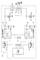
- FIG. 4 shows a circuit configuration for one Peltier element P (that is, one of Peltier element Pa and Peltier element Pb). That is, the Peltier driver 50 according to the present embodiment has a circuit configuration for the Peltier element Pa and a circuit configuration for the Peltier element Pb.
- the circuit configuration for one Peltier element P will be described, and the circuit configuration for the other Peltier element P will be described in the same way, and the description thereof will be omitted.
- the Peltier driver 50 includes a driver control unit 51, a first output voltage control unit 52, a second output voltage control unit 53, a first output voltage adjustment unit 54, The second output voltage adjusting unit 55, the first transistor FETa, the second transistor FETb, and the relay switch SW are provided, and drive control of one Peltier element P (Peltier element Pa or Peltier element Pb) is performed. .
- the driver control unit 51 performs an operation related to drive control of one Peltier element P (see FIGS. 5 to 10) based on temperature information input via the laser controller 5, and drives one Peltier element P. Serves as the center of control.
- the driver control unit 51 outputs a Peltier control enable signal (Peltier control EN signal) and a polarity switching signal. Then, an enable signal (ENa ON / OFF signal) is output from the driver control unit 51 to the DC / DC converter DDCa of the first output voltage adjustment unit 54. Further, an enable signal (ENb ON / OFF signal) is output from the driver control unit 51 to the DC / DC converter DDCb of the second output voltage adjustment unit 55.
- the driver control unit 51 outputs gate signals (FETa ON / OFF signal, FETb ON / OFF signal) to the first transistor FETa and the second transistor FETb, respectively.
- the first transistor FETa and the second transistor FETb are configured by N-channel MOSFET transistors.
- the first output voltage control unit 52 includes a digital potentiometer having a variable resistor.
- the first output voltage control unit 52 variably controls the resistance value of the variable resistor in the first output voltage control unit 52 according to the resistance signal input from the driver control unit 51.
- the second output voltage control unit 53 includes a digital potentiometer having a variable resistor.
- the second output voltage control unit 53 variably controls the resistance value of the second output voltage control unit 53 according to the resistance signal input from the driver control unit 51.
- the driver control unit 51 is configured to include a CPLD (Complex Programmable Logic Device) separately from the CPU 61. From the driver control unit 51 to the first output voltage control unit 52 and the second output voltage control unit 53. In order to transmit the resistance signal, a communication method such as SPI (Serial Peripheral Interface) or I2C (Inter-Integrated Circuit) is used.
- SPI Serial Peripheral Interface
- I2C Inter-Integrated Circuit
- the first output voltage adjustment unit 54 includes a DC / DC converter DDCa, a coil La, and a capacitor Ca.
- the DC / DC converter DDCa has a Vfb terminal, an EN terminal, and an OUT terminal.
- the coil La is electrically connected between the OUT terminal of the DC / DC converter DDCa and the first output terminal Oa of the first output voltage adjustment unit 54.
- a capacitor Ca is electrically connected between the first output terminal Oa of the first output voltage adjustment unit 54 and the ground voltage.
- the DC / DC converter DDCa, the coil La, and the capacitor Ca constitute a synchronous rectification step-down chopper type DC / DC converter.
- variable resistor and the fixed resistor of the digital potentiometer in the first output voltage control unit 52 are electrically connected in series between the first output terminal Oa of the first output voltage adjustment unit 54 and the ground voltage.
- the connection point between the variable resistor and the fixed resistor in the first output voltage control unit 52 is electrically connected to the Vfb terminal of the DC / DC converter DDCa in the first output voltage adjustment unit 54.
- An enable signal (ENa ON / OFF signal) is input to the EN terminal of the DC / DC converter DDCa.
- the DC / DC converter DDCa has a voltage substantially equal to the predetermined reference voltage Vref during the period when a high level enable signal (ENa ON / OFF signal: ON) is input to the EN terminal. And output from the first output terminal Oa.
- the output voltage at this time is referred to as a first output voltage Va.
- the first output terminal Oa of the first output voltage adjustment unit 54 is electrically connected to the first terminal Ta of the Peltier element P.
- the first output voltage Va of the first output voltage adjustment unit 54 is determined by the following equation based on the resistance value of the variable resistor, the resistance value of the fixed resistor, and the reference voltage Vref in the first output voltage control unit 52.
- Va Vref (1 + resistance value of variable resistance / resistance value of fixed resistance) (1)
- the resistance value of the variable resistor and the resistance value of the fixed resistor in Equation (1) are the resistance value related to the variable resistor of the digital potentiometer constituting the first output voltage control unit 52, and the fixed resistance in the first output voltage control unit 52. Means the resistance value.
- the reference voltage Vref indicates a voltage value (for example, 0.8 V) of the reference voltage built in the DC / DC converter DDCa.
- the second output voltage adjustment unit 55 includes a DC / DC converter DDCb, a coil Lb, and a capacitor Cb. Similar to the DC / DC converter DDCa, the DC / DC converter DDCb has a Vfb terminal, an EN terminal, and an OUT terminal.
- the coil Lb is electrically connected between the OUT terminal of the DC / DC converter DDCb and the second output terminal Ob of the second output voltage adjusting unit 55.
- a capacitor Cb is electrically connected between the second output terminal Ob of the second output voltage adjustment unit 55 and the ground voltage.
- the DC / DC converter DDCb, the coil Lb, and the capacitor Cb constitute a synchronous rectification step-down chopper DC / DC converter.
- variable resistor and the fixed resistor of the digital potentiometer in the second output voltage control unit 53 are electrically connected in series between the second output terminal Ob of the second output voltage adjustment unit 55 and the ground voltage.
- the Vfb terminal of the DC / DC converter DDCb in the second output voltage adjustment unit 55 is electrically connected to a connection point between the variable resistor and the fixed resistor in the second output voltage control unit 53.
- An enable signal (ENb ON / OFF signal) is input to the EN terminal of the DC / DC converter DDCb.
- the DC / DC converter DDCb predetermines the voltage input to the Vfb terminal during the period when the high level enable signal (ENa ON / OFF signal: ON) is input to the EN terminal. Is controlled to a voltage substantially equal to the reference voltage Vref and output from the second output terminal Ob. The output voltage at this time is referred to as a second output voltage Vb.
- the second output terminal Ob of the second output voltage adjustment unit 55 is electrically connected to the second terminal Tb of the Peltier element P.
- the resistance value of the variable resistor and the resistance value of the fixed resistor in Equation (2) are the resistance value related to the variable resistor of the digital potentiometer constituting the second output voltage control unit 53, and the fixed resistance in the second output voltage control unit 53. Means the resistance value.
- the reference voltage Vref indicates a voltage value (for example, 0.8 V) of the reference voltage built in the DC / DC converter DDCb.
- the switching frequency of the DC / DC converter DDCa and the switching frequency of the DC / DC converter DDCb are, for example, several Hz to several MHz.
- the inductances of the coil La and the coil Lb are, for example, several ⁇ H to several tens ⁇ H.
- the capacitance values of the capacitor Ca and the capacitor Cb are, for example, several hundred ⁇ F to 1000 ⁇ F in order to stably supply the output voltages of the first output voltage adjustment unit 54 and the second output voltage adjustment unit 55.
- the voltage range of the first output voltage Va and the second output voltage Vb is based on the above-described formulas (1) and (2), and is, for example, 0.8V to 20V, and more than 20V. Is also possible.
- the resistance value of the variable resistor in the first output voltage control unit 52 and the second output voltage control unit 53 By setting the resistance value of the variable resistor in the first output voltage control unit 52 and the second output voltage control unit 53, the first output voltage Va and the second output voltage Vb are linearly changed in the above voltage range. Can do.
- the first transistor FETa is composed of an N-channel MOSFET transistor, and has a gate terminal, a source terminal, and a drain terminal.
- the first transistor FETa controls the current between the source terminal and the drain terminal by applying a voltage to the gate terminal.
- a gate signal (FETa ON / OFF signal) is input to the gate terminal of the first transistor FETa.
- the source terminal of the first transistor FETa is electrically connected to the ground voltage
- the drain terminal of the first transistor FETa is electrically connected to the first output terminal Oa of the first output voltage adjustment unit 54.
- the second transistor FETb is composed of an N-channel MOSFET transistor, and has a gate terminal, a source terminal, and a drain terminal.
- the second transistor FETb controls the current between the source terminal and the drain terminal by applying a voltage to the gate terminal.
- a gate signal (FETb ON / OFF signal) is input to the gate terminal of the second transistor FETb.
- the source terminal of the second transistor FETb is electrically connected to the ground voltage
- the drain terminal of the second transistor FETb is electrically connected to the second output terminal Ob of the second output voltage adjustment unit 55.
- the high level voltage value of the gate signal (FETa ON / OFF signal, FETb ON / OFF signal) is, for example, 10V.
- the relay switch SW is disposed between the first terminal Ta of the Peltier element P, the drain terminal of the first transistor FETa, and the first output terminal Oa of the first output voltage adjustment unit 54, and receives an electrical signal. Are configured to open and close.
- the relay switch SW disconnects the electrical connection to the Peltier element P when the power supply voltage from the power supply Vcc is disconnected.
- the driver control unit 51 outputs a high level enable signal (ENa ON / OFF signal: ON) to the DC / DC converter DDCa of the first output voltage adjustment unit 54 and at the same time, a low level enable signal (ENb). ON / OFF signal: OFF) is output to the DC / DC converter DDCb of the second output voltage adjustment unit 55.
- the DC / DC converter DDCA of the first output voltage adjustment unit 54 operates, and the first output voltage adjustment unit 54 outputs the first output voltage Va.
- the second output terminal Ob of the second output voltage adjustment unit 55 is in an open state or a high impedance state.
- the driver control unit 51 outputs a high level gate signal (FETb ON / OFF signal: ON) to the second transistor FETb, and outputs a low level gate signal (FETa ON / OFF signal: OFF) to the first transistor FETb. Output to the transistor FETa. As a result, the second transistor FETb is turned on and the first transistor FETa is turned off.
- the Peltier driver 50 the first output terminal Oa of the first output voltage adjusting unit 54, the first terminal Ta of the Peltier element P, the second terminal Tb, the drain terminal, the source terminal of the second transistor FETb, the ground Current flows through a path in the order of voltage. That is, since a current flows from the first terminal Ta of the Peltier element P toward the second terminal Tb, the surface of the Peltier element P on the side to be controlled (for example, the excitation semiconductor laser unit 40) absorbs heat. That is, the Peltier driver 50 can cool the control target (for example, the pumping semiconductor laser unit 40) by performing drive control of the Peltier element P.
- the control target for example, the pumping semiconductor laser unit 40
- the driver control unit 51 outputs a high level enable signal (ENb ON / OFF signal: ON) to the DC / DC converter DDCb of the second output voltage adjustment unit 55 and at the same time, a low level enable signal (ENa ON / OFF signal: OFF) is output to the DC / DC converter DDCa of the first output voltage adjustment unit 54.
- the DC / DC converter DDCb of the second output voltage adjustment unit 55 operates, and the second output voltage adjustment unit 55 outputs the second output voltage Vb.
- the first output terminal Oa of the first output voltage adjustment unit 54 is in an open state or a high impedance state.
- the driver control unit 51 outputs a high level gate signal (FETa ON / OFF signal: ON) to the first transistor FETa, and outputs a low level gate signal (FETb ON / OFF signal: OFF) to the second transistor FETa. Output to the transistor FETb. As a result, the first transistor FETa is turned on and the second transistor FETb is turned off.
- the Peltier driver 50 the second output terminal Ob of the second output voltage adjusting unit 55, the second terminal Tb of the Peltier element Pa, the first terminal Ta, the drain terminal, the source terminal of the first transistor FETa, the ground Current flows through a path in the order of voltage. That is, since a current flows from the second terminal Tb of the Peltier element Pa to the first terminal Ta, the surface of the Peltier element P on the side to be controlled (for example, the excitation semiconductor laser unit 40) is heated. That is, the Peltier driver 50 can heat the control target (for example, the pumping semiconductor laser unit 40) by performing drive control of the Peltier element P.
- the control target for example, the pumping semiconductor laser unit 40
- the processing contents relating to the drive control of the Peltier element P executed in the Peltier driver 50 will be described in detail with reference to FIGS.
- the drive control of the Peltier element P is performed by the driver control unit 51 of the Peltier driver 50 based on various information such as the temperature information of the temperature sensor 36 and the temperature sensor 37 input from the laser controller 5 (for example, , The first output voltage adjustment unit 54 and the like) is controlled mainly.
- the driver control unit 51 first determines in S1 whether or not the voltage of the power supply Vcc is equal to or higher than a predetermined value (18V).
- a predetermined value 18V
- the driver control unit 51 shifts the process to S2.
- the driver control unit 51 performs the process until the power supply Vcc becomes equal to or higher than the predetermined value. stand by.
- the driver control unit 51 outputs a high level gate signal (FETa ON / OFF signal: ON) to the first transistor FETa and outputs a high level gate signal (FETb ON / OFF signal: ON). Output to 2-transistor FETb. As a result, the first transistor FETa and the second transistor FETb are turned on. Thereafter, the driver control unit 51 proceeds to S3.
- the driver control unit 51 outputs an electrical signal to the relay switch SW to turn on the relay switch SW. As described above, since the first transistor FETa and the second transistor FETb are on, both ends of the Peltier element P are short-circuited. After the relay switch SW is turned on, the driver control unit 51 proceeds to S4.
- the driver control unit 51 After shifting to S4, the driver control unit 51 performs temperature adjustment processing and performs drive control of the Peltier element P, thereby adjusting the temperature of the control target (for example, the laser oscillator 21 or the excitation semiconductor laser unit 40). Do. In the temperature adjustment process (S4), the driver control unit 51 performs a cooling drive of the Peltier element P, a heating drive of the Peltier element P, and the like as shown in FIG. Alternatively, the pumping semiconductor laser unit 40) is maintained within a predetermined temperature range. The contents of the temperature adjustment process (S4) will be described later in detail with reference to FIG. Thereafter, the driver control unit 51 shifts the processing to S5.
- the driver control unit 51 shifts the processing to S5.
- the driver control unit 51 executes a sleep process in order to shift to a sleep state in which the drive control of the Peltier element P is awaited.
- the details of the sleep process (S5) will be described later in detail with reference to FIG.
- the driver control unit 51 proceeds to S6.
- the driver control unit 51 determines whether or not a temperature adjustment instruction is received from the laser controller 5.
- the temperature adjustment instruction is output from the laser controller 5 when the CPU 61 of the laser controller 5 determines that drive control of the Peltier element P is necessary based on the temperature sensor 36 and the temperature information of the temperature sensor 36.
- the driver control unit 51 returns the process to the temperature adjustment process (S4).
- the driver control unit 51 proceeds to S7.
- the driver control unit 51 determines whether or not the voltage of the power supply Vcc is equal to or lower than a predetermined value (18V). When the voltage of the power supply Vcc is equal to or lower than the predetermined value (S7: YES), the driver control unit 51 ends the process related to the drive control of the Peltier element P. On the other hand, when the voltage of the power supply Vcc is not less than or equal to the predetermined value (S7: NO), the driver control unit 51 returns the process to S6.
- the driver control unit 51 determines that the temperature detected by the temperature sensor 36 is the set temperature of the control target (for example, the excitation semiconductor laser unit 40) based on the temperature information acquired from the laser controller 5. It is determined whether it is below the range (S11). If the detected temperature is not less than or equal to the set temperature range (S11: NO), the driver control unit 51 proceeds to S12. On the other hand, when the detected temperature is equal to or lower than the set temperature range (S11: YES), the driver control unit 51 proceeds to S16.
- the set temperature of the control target for example, the excitation semiconductor laser unit 40
- the driver control unit 51 outputs a high-level polarity switching signal.
- the high-level polarity switching signal indicates cooling driving of the Peltier element P. After outputting the high-level polarity switching signal, the driver control unit 51 proceeds to S13.
- the driver control unit 51 sets the first output voltage Va from the first output voltage adjustment unit 54 to the minimum value by changing the resistance value of the variable resistor in the first output voltage control unit 52. After setting the first output voltage Va to the minimum value, the driver control unit 51 proceeds to S14.
- the driver control unit 51 outputs a high-level Peltier control EN signal to drive the Peltier element P. After outputting the high level Peltier control EN signal, the driver control unit 51 proceeds to S15.
- the driver control unit 51 outputs a high level enable signal (ENa ON / OFF signal: ON) to the DC / DC converter DDCa of the first output voltage adjustment unit 54, and a low level gate signal (FETa). ON / OFF signal: OFF) is output to the first transistor FETa. After outputting the control signal to the first output voltage adjustment unit 54 and the first transistor FETa, the driver control unit 51 proceeds to S20.
- ENa ON / OFF signal: ON to the DC / DC converter DDCa of the first output voltage adjustment unit 54
- FETa low level gate signal
- the operation of the second output voltage adjustment unit 55 remains stopped and the second transistor FETb is on, so that the current in the Peltier driver 50 is the first output terminal Oa of the first output voltage adjustment unit 54,
- the first terminal Ta of the Peltier element P, the second terminal Tb, the drain terminal of the second transistor FETb, the source terminal, and the ground voltage can flow in this order. That is, the Peltier driver 50 can cool the Peltier element P.
- the driver control unit 51 outputs a low-level polarity switching signal.
- the low level polarity switching signal indicates heating driving of the Peltier element P. After outputting the low-level polarity switching signal, the driver control unit 51 proceeds to S17.
- the driver control unit 51 sets the second output voltage Vb from the second output voltage adjustment unit 55 to the minimum value by changing the resistance value of the variable resistor in the second output voltage control unit 53. . After setting the second output voltage Vb to the minimum value, the driver control unit 51 proceeds to S18.
- the driver control unit 51 outputs a high-level Peltier control EN signal to drive the Peltier element P. After outputting the high level Peltier control EN signal, the driver control unit 51 proceeds to S19.
- the driver control unit 51 outputs a high level enable signal (ENb ON / OFF signal: ON) to the DC / DC converter DDCb of the second output voltage adjustment unit 55, and a low level gate signal (FETb ON / OFF signal: OFF) is output to the second transistor FETb.
- ENb ON / OFF signal ON
- FETb ON / OFF signal OFF
- the current in the Peltier driver 50 is supplied to the second output terminal Ob of the second output voltage adjustment unit 55,
- the second terminal Tb of the Peltier element Pa, the first terminal Ta, the drain terminal of the first transistor FETa, the source terminal, and the ground voltage can flow in this order. That is, the Peltier driver 50 can heat the Peltier element P.
- the driver control unit 51 determines whether or not a predetermined period (for example, 100 ms) has elapsed since the previous detection of the ambient temperature based on the temperature information acquired from the laser controller 5.
- a predetermined period for example, 100 ms
- the driver control unit 51 proceeds to S21.
- the driver control unit 51 waits for processing until the predetermined period elapses.
- the driver control unit 51 has a temperature detected by the temperature sensor 36 that is equal to or lower than the set temperature range of the control target (for example, the excitation semiconductor laser unit 40). Determine whether or not.
- the driver control unit 51 shifts the process to the cooling drive process (S22).
- the driver control unit 51 shifts the process to the heating drive process (S23).
- the driver control unit 51 cools the control target (for example, the excitation semiconductor laser unit 40) using the Peltier element P by executing the cooling drive process.
- the details of the cooling drive process (S22) will be described in detail with reference to FIG. After completing the cooling drive process (S22), the driver control unit 51 proceeds to S24.
- the driver control unit 51 heats the control target (for example, the excitation semiconductor laser unit 40) using the Peltier element P by executing the heating drive process.
- the control target for example, the excitation semiconductor laser unit 40
- the driver control unit 51 proceeds to S24.
- the driver control unit 51 determines whether or not a sleep instruction is received from the laser controller 5.
- the sleep instruction is, for example, when the period during which no operation is performed on the laser processing apparatus 1 continues for a predetermined period or longer and there is no need to adjust the temperature of the control target using the Peltier element P. Is output from the CPU 61.
- the driver control unit 51 ends the temperature adjustment process (S4).
- the driver control unit 51 returns the process to S20 and continues the temperature adjustment of the control target using the Peltier element P.
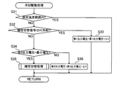
- the driver control unit 51 determines the temperature detected by the temperature sensor based on the temperature information acquired from the laser controller 5 to be the set temperature range of the control target (for example, the excitation semiconductor laser unit 40). It is judged whether it is in (S31). When the detected temperature is within the set temperature range to be controlled (S31: YES), the driver control unit 51 ends the cooling drive process as it is. On the other hand, when the detected temperature is not within the set temperature range to be controlled (S31: NO), the driver control unit 51 shifts the process to S32.
- the driver control unit 51 determines whether or not the current polarity switching signal is at a high level indicating cooling driving of the Peltier element P.
- the driver control unit 51 proceeds to S33.
- the driver control unit 51 proceeds to S34.
- the driver control unit 51 controls the variable resistance of the first output voltage control unit 52 to increase the first output voltage Va from the first output voltage adjustment unit 54 in a stepwise manner. That is, the driver control unit 51 adds a predetermined value (that is, ⁇ V) to the first output voltage Va.
- the Peltier element P can control the amount of heat transfer according to the current value flowing from one surface to the other surface of the Peltier element P. Therefore, by increasing the first output voltage Va stepwise, The heat absorption efficiency is further increased, and the controlled object is more actively cooled. After raising the first output voltage Va by one step, the driver control unit 51 ends the cooling drive process.
- the driver control unit 51 determines whether or not the second output voltage Vb of the second output voltage adjustment unit 55 is the minimum voltage in the second output voltage adjustment unit 55.
- the driver control unit 51 proceeds to S35.
- the driver control unit 51 proceeds to S36.
- the driver control unit 51 executes a polarity switching process to switch the Peltier element P from the heating drive state to the cooling drive state.
- the contents of the polarity switching process (S35) will be described later in detail with reference to FIG.
- the driver control unit 51 ends the cooling drive process.
- the driver control unit 51 controls the variable resistance of the second output voltage control unit 53, thereby gradually reducing the second output voltage Vb of the second output voltage adjustment unit 55.
- the heating efficiency of the Peltier element P can be lowered, and therefore the amount of heat applied by the Peltier element P can be made lower than the amount of heat released by natural heat dissipation or the like in the controlled object.
- the driver control unit 51 can gently cool the controlled object by using natural heat dissipation or the like by driving and controlling the Peltier element P.
- the driver control unit 51 ends the cooling drive process.
- the driver control unit 51 determines that the temperature detected by the temperature sensor is the set temperature range of the control target (for example, the excitation semiconductor laser unit 40) based on the temperature information acquired from the laser controller 5. It is judged whether it is in (S41). When the detected temperature is within the set temperature range to be controlled (S41: YES), the driver control unit 51 ends the heating drive process as it is. On the other hand, when the detected temperature is not within the set temperature range to be controlled (S41: NO), the driver control unit 51 proceeds to S42.
- the set temperature range of the control target for example, the excitation semiconductor laser unit 40
- the driver control unit 51 determines whether or not the current polarity switching signal is at a low level indicating heating driving of the Peltier element P.
- the driver control unit 51 proceeds to S43.
- the driver control unit 51 proceeds to S44.
- the driver control unit 51 controls the variable resistance of the second output voltage control unit 53 to increase the second output voltage Vb from the second output voltage adjustment unit 55 in a stepwise manner. That is, by increasing the second output voltage Vb stepwise, the heating efficiency of the Peltier element P is further increased, and the controlled object is more actively heated. After raising the second output voltage Vb by one step, the driver control unit 51 ends the heating drive process.
- the driver control unit 51 determines whether or not the first output voltage Va of the first output voltage adjustment unit 54 is the minimum voltage in the first output voltage adjustment unit 54.
- the driver control unit 51 proceeds to S45.
- the driver control unit 51 proceeds to S46.
- the driver control unit 51 executes a polarity switching process to switch the Peltier element P from the cooling drive state to the heating drive state.
- the contents of the polarity switching process (S45) will be described later in detail with reference to FIG.
- the driver control unit 51 ends the heating drive process.
- the driver control unit 51 controls the variable resistance of the first output voltage control unit 52 to decrease the first output voltage Va of the first output voltage adjustment unit 54 in a stepwise manner.
- the heat absorption efficiency of the Peltier element P can be lowered.
- the driver control unit 51 can gently heat the control target using heat generated in the control target itself by controlling the drive of the Peltier element P. After the first output voltage Va is lowered by one step, the driver control unit 51 ends the heating drive process.
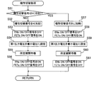
- the driver control unit 51 determines whether or not the current polarity switching signal is at a high level indicating cooling driving of the Peltier element P (S51).
- the driver control unit 51 proceeds to S52.
- the driver control unit 51 proceeds to S57.
- the driver control unit 51 switches and sets the polarity switching signal from a low level indicating the heating driving of the Peltier element P to a high level indicating the cooling driving of the Peltier element P. After setting the polarity switching signal to the high level, the driver control unit 51 proceeds to S53.
- the driver control unit 51 outputs a low level enable signal (ENb ON / OFF signal: OFF) to the DC / DC converter DDCb of the second output voltage adjustment unit 55, and a high level gate signal (FETb ON / OFF signal: ON) is output to the second transistor FETb.
- ENb ON / OFF signal: OFF a low level enable signal
- FETb ON / OFF signal: ON a high level gate signal
- the Peltier driver 50 is in a state where the second output voltage adjustment unit 55 is operated and the operation of the first output voltage control unit 52 is stopped in order to perform the heating drive of the Peltier element P.
- the first transistor FETa is turned on and the second transistor FETb is turned off.
- S53 by outputting a control signal to the second output voltage adjusting unit 55 and the second transistor FETb, it is possible to turn on the second transistor FETb while stopping the operation of the second output voltage adjusting unit 55. it can.
- the operation of the first output voltage adjustment unit 54 and the second output voltage adjustment unit 55 is stopped, the power supply to the Peltier element P is stopped. Further, since the first transistor FETa and the second transistor FETb are turned on, both ends of the Peltier element P are short-circuited. Therefore, even when the Seebeck voltage due to the temperature difference between both surfaces of the Peltier element P is generated, the influence of the Seebeck voltage on the first output voltage adjusting unit 54, the second output voltage adjusting unit 55, etc. can be cut off. it can.
- the driver control unit 51 controls the variable resistance of the first output voltage control unit 52 to set the first output voltage Va from the first output voltage adjustment unit 54 to the minimum voltage. After setting the first output voltage Va to the minimum voltage, the driver control unit 51 proceeds to S55.
- the driver control unit 51 waits until a predetermined period (for example, 50 ms) elapses after setting the first output voltage Va to the minimum voltage. After the predetermined period has elapsed, the driver control unit 51 proceeds to S56.
- a predetermined period for example, 50 ms
- the driver control unit 51 outputs a high level enable signal (ENa ON / OFF signal: ON) to the DC / DC converter DDCa of the first output voltage adjustment unit 54, and a low level gate signal (FETa ON). / OFF signal: OFF) is output to the first transistor FETa.
- ENa ON / OFF signal ON
- FETa ON low level gate signal
- the Peltier driver 50 turns off the first transistor FETa with the first output voltage control unit 52 operating and the second output voltage adjusting unit 55 stopped.
- the two-transistor FETb is turned on. That is, the current flows in the order of the first output terminal Oa of the first output voltage adjusting unit 54, the first terminal Ta, the second terminal Tb, the drain terminal, the source terminal, and the ground voltage of the Peltier element P.
- the Peltier element P can be driven to be cooled. That is, by performing the processing of S52 to S56, the polarity of the Peltier element P can be switched from the heating drive state to the cooling drive state.
- the driver control unit 51 changes the polarity switching signal from the high level indicating the cooling drive of the Peltier element P to the Peltier element P. Switch to low level to indicate heating drive. After setting the polarity switching signal to the low level, the driver control unit 51 proceeds to S58.
- the driver control unit 51 outputs a low level enable signal (ENa ON / OFF signal: OFF) to the DC / DC converter DDCa of the first output voltage adjustment unit 54, and a high level gate signal (FETa ON). / OFF signal: ON) is output to the first transistor FETa.
- the driver control unit 51 proceeds to S59.
- the Peltier driver 50 is in a state where the first output voltage control unit 52 is operated and the operation of the second output voltage adjustment unit 55 is stopped in order to perform the cooling drive of the Peltier element P.
- the first transistor FETa is turned off and the second transistor FETb is turned on.
- S58 by outputting a control signal to the first output voltage adjusting unit 54 and the first transistor FETa, it is possible to turn on the first transistor FETa while stopping the operation of the first output voltage adjusting unit 54. it can.
- the driver control unit 51 controls the variable resistance of the second output voltage control unit 53 to set the second output voltage Vb from the second output voltage adjustment unit 55 to the minimum voltage. After setting the second output voltage Vb to the minimum voltage, the driver control unit 51 proceeds to S60.
- the driver control unit 51 waits until a predetermined period (for example, 50 ms) elapses after setting the second output voltage Vb to the minimum voltage. After the predetermined period has elapsed, the driver control unit 51 proceeds to S61.
- a predetermined period for example, 50 ms
- the driver control unit 51 outputs a high level enable signal (ENb ON / OFF signal: ON) to the DC / DC converter DDCb of the second output voltage adjustment unit 55, and a low level gate signal (FETb ON). / OFF signal: OFF) is output to the second transistor FETb.
- ENb ON / OFF signal ON
- FETb ON low level gate signal
- the Peltier driver 50 turns on the first transistor FETa with the second output voltage adjustment unit 55 operating and the first output voltage control unit 52 stopped operating,
- the two-transistor FETb is turned off. That is, the current flows in the order of the second output terminal Ob of the second output voltage adjustment unit 55, the second terminal Tb of the Peltier element Pa, the first terminal Ta, the drain terminal of the first transistor FETa, the source terminal, and the ground voltage.
- the Peltier element P can be driven by heating. That is, the polarity of the Peltier element P can be switched from the cooling drive state to the heating drive state by performing the processes of S57 to S61.
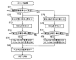
- the driver control unit 51 determines whether or not the current polarity switching signal is at a high level indicating cooling driving of the Peltier element P (S71). If the polarity switching signal is at the high level (S71: YES), the driver control unit 51 proceeds to S72. On the other hand, when the polarity switching signal is not at the high level (S71: NO), the driver control unit 51 proceeds to S76.
- the driver control unit 51 controls the variable resistance of the first output voltage control unit 52, thereby gradually reducing the first output voltage Va of the first output voltage adjustment unit 54 for each predetermined voltage.
- the predetermined voltage at this time is set within a range in which the temperature responsiveness of the Peltier element P can follow within 100 ms, and is about 1 V in this embodiment.
- the temperature responsiveness of the Peltier element P tends to require a certain amount of time, and even if the first output voltage Va of the first output voltage adjustment unit 54 is suddenly lowered, The temperature difference between the first terminal Ta and the second terminal Tb does not become small immediately.
- the period corresponding to the temperature responsiveness of the Peltier element P can be secured by lowering the first output voltage Va step by step for each predetermined voltage.
- the driver control unit 51 proceeds to S73.
- the driver control unit 51 counts 100 ms after reducing the first output voltage Va by one step. Then, the driver control unit 51 proceeds to S74 after the count of 100 ms is completed.
- the driver control unit 51 determines whether or not the first output voltage Va of the first output voltage adjustment unit 54 is the minimum voltage in the first output voltage adjustment unit 54.
- the driver control unit 51 proceeds to S75.
- the driver control unit 51 returns the process to S72 in order to further reduce the first output voltage Va by one step.
- the driver control unit 51 outputs a low-level enable signal (ENa ON / OFF signal: OFF) to the DC / DC converter DDCa of the first output voltage adjustment unit 54, and a high-level gate signal (FETa ON / OFF signal: ON) is output to the first transistor FETa.
- the driver control unit 51 proceeds to S80.
- the Peltier driver 50 stops the operation of the second output voltage adjustment unit 55 by operating the first output voltage control unit 52 in order to perform the cooling drive of the Peltier element P.
- the first transistor FETa is turned off and the second transistor FETb is turned on.
- S75 by outputting a control signal to the first output voltage adjustment unit 54 and the first transistor FETa, it is possible to turn on the first transistor FETa while stopping the operation of the first output voltage adjustment unit 54. it can.
- the operations of the first output voltage adjustment unit 54 and the second output voltage adjustment unit 55 are stopped, the power supply to the Peltier element P is stopped. Further, since the first transistor FETa and the second transistor FETb are turned on, both ends of the Peltier element P are short-circuited. Therefore, even when the Seebeck voltage due to the temperature difference between both surfaces of the Peltier element P is generated, the influence of the Seebeck voltage on the first output voltage adjusting unit 54, the second output voltage adjusting unit 55, etc. can be cut off. it can. At this time, since the first output voltage Va is the minimum voltage, the temperature difference between both surfaces of the Peltier element P can be reduced, and the Seebeck voltage can be suppressed low. That is, according to the Peltier driver 50, by suppressing the Seebeck voltage of the Peltier element P to be low, the first transistor FETa and the second transistor FETb can be prevented from being damaged by the Seebeck voltage.
- the driver control unit 51 controls the variable resistance of the second output voltage control unit 53, thereby decreasing the second output voltage Vb of the second output voltage adjustment unit 55 step by step for each predetermined voltage.
- the predetermined voltage at this time is set within a range in which the temperature responsiveness of the Peltier element P can follow within 100 ms, and is about 1 V in this embodiment.
- the temperature responsiveness of the Peltier element P tends to require a certain amount of time, and even if the second output voltage Vb of the second output voltage adjustment unit 55 is suddenly lowered, The temperature difference between the first terminal Ta and the second terminal Tb does not become small immediately.
- the driver control unit 51 proceeds to S77.
- the driver control unit 51 counts 100 ms after lowering the second output voltage Vb by one step. Then, the driver control unit 51 proceeds to S78 after the count of 100 ms is completed.
- the driver control unit 51 determines whether or not the second output voltage Vb of the second output voltage adjustment unit 55 is the minimum voltage in the second output voltage adjustment unit 55. If the second output voltage Vb is the minimum voltage (S78: YES), the driver control unit 51 proceeds to S79. On the other hand, when the second output voltage Vb is not the minimum voltage (S78: NO), the driver control unit 51 returns the process to S76 in order to lower the second output voltage Vb by one step.
- the driver control unit 51 outputs a low-level enable signal (ENb ON / OFF signal: OFF) to the DC / DC converter DDCb of the second output voltage adjustment unit 55, and a high-level gate signal ( FETb ON / OFF signal: ON) is output to the second transistor FETb.
- ENb ON / OFF signal: OFF a low-level enable signal
- FETb ON / OFF signal: ON a high-level gate signal
- the driver control unit 51 proceeds to S80.
- the Peltier driver 50 stops the operation of the first output voltage control unit 52 by operating the second output voltage adjusting unit 55 in order to drive the Peltier element P to be heated.
- the second transistor FETb is turned off and the first transistor FETa is turned on.
- the second transistor FETb can be turned on while stopping the operation of the second output voltage adjustment unit 55. it can.
- the operations of the first output voltage adjustment unit 54 and the second output voltage adjustment unit 55 are stopped, the power supply to the Peltier element P is stopped. Further, since the first transistor FETa and the second transistor FETb are turned on, both ends of the Peltier element P are short-circuited. Therefore, even when the Seebeck voltage due to the temperature difference between both surfaces of the Peltier element P is generated, the influence of the Seebeck voltage on the first output voltage adjusting unit 54, the second output voltage adjusting unit 55, etc. can be cut off. it can. At this time, since the second output voltage Vb is the minimum voltage, the temperature difference between both surfaces of the Peltier element P can be reduced, and the Seebeck voltage can be suppressed low. That is, according to the Peltier driver 50, by suppressing the Seebeck voltage of the Peltier element P to be low, the first transistor FETa and the second transistor FETb can be prevented from being damaged by the Seebeck voltage.
- the driver control unit 51 outputs a low-level Peltier control EN signal, stops driving the Peltier element P, and shifts to the sleep state. After outputting the low-level Peltier control EN signal, the driver control unit 51 ends the sleep process.
- the Peltier driver 50 includes the driver control unit 51, the first output voltage control unit 52, the second output voltage control unit 53, the first output voltage adjustment unit 54, and the second A temperature that includes the output voltage adjustment unit 55, the first transistor FETa, and the second transistor FETb, and that indicates the ambient temperature of the control target (for example, the excitation semiconductor laser unit 40) detected by the temperature sensor 36 or the like.
- the drive control of the Peltier element P can be performed, and thus the temperature control regarding the controlled object can be performed.
- the Peltier driver 50 when driving of the first output voltage adjusting unit 54 and the second output voltage adjusting unit 55 is stopped and power supply to the Peltier element P is stopped, the Seebeck effect is generated in the Peltier element P. A Seebeck voltage corresponding to the temperature difference in the Peltier element P can be generated.
- the first transistor FETa and the second transistor By turning on the transistor FETb, the first terminal Ta and the second terminal Tb of the Peltier element P can be short-circuited.
- the Seebeck voltage generated in the Peltier element P is another component (for example, the first output voltage adjustment unit 54, the second output voltage adjustment unit 55, etc.) that configures the Peltier driver 50. Can be prevented, and problems such as breakage and malfunction of the Peltier driver 50 and its components can be prevented.
- the driver control unit 51 performs the first output.
- the driving of the voltage adjusting unit 54 is stopped and the first transistor FETa is turned on (S58).
- the second output voltage adjusting unit 55 is driven and the second transistor FETb is turned off (S61). That is, according to the Peltier driver 50, the Peltier element P can be reliably switched from the cooling drive state to the heating drive state.
- the driving of the first output voltage adjusting unit 54 is stopped and the first transistor FETa is turned on (S58).
- the first terminal Ta and the second terminal Tb of the Peltier element P can be short-circuited, thereby preventing problems such as damage or malfunction of the Peltier driver 50 and its components due to the Seebeck voltage generated in the Peltier element P. be able to.
- the driver control unit 51 when the Peltier element P driven in the heating drive state is switched to the cooling drive state in the polarity switching process (S35, S45), the driver control unit 51 outputs the second output.
- the driving of the voltage adjusting unit 55 is stopped and the second transistor FETb is turned on (S53).
- the first output voltage adjusting unit 54 is driven and the first transistor FETa is turned off (S56). That is, according to the Peltier driver 50, the Peltier element P can be reliably switched from the heating drive state to the cooling drive state.
- the driving of the second output voltage adjusting unit 55 is stopped and the second transistor FETb is turned on (S53).
- the first terminal Ta and the second terminal Tb of the Peltier element P can be short-circuited, thereby preventing problems such as damage or malfunction of the Peltier driver 50 and its components due to the Seebeck voltage generated in the Peltier element P. be able to.
- the driver control unit 51 causes the first output voltage adjustment unit 54 and When stopping any driving of the second output voltage adjusting unit 55, the first transistor FETa and the second transistor FETb are turned on (S75, S79), and the first terminal Ta and the second terminal Tb of the Peltier element P are turned on. Can be short-circuited.
- the Peltier driver 50 it is possible to prevent problems such as breakage or malfunction of the Peltier driver 50 and its constituent elements due to the Seebeck voltage generated in the Peltier element P when shifting to the sleep state.
- the Peltier driver 50 when receiving a temperature adjustment instruction from the laser controller 5 (S6: YES), canceling the sleep state and restarting the drive control of the Peltier driver 50, the driver control unit 51 Then, one of the cooling drive control (S12 to S15) and the heating drive control (S16 to S19) of the Peltier element P is executed. Thereby, even when the Peltier driver 50 cancels the sleep state, the Peltier driver 50 can appropriately perform temperature control on the control target (for example, the excitation semiconductor laser unit 40 and the laser oscillator 21).
- the control target for example, the excitation semiconductor laser unit 40 and the laser oscillator 21.
- the first transistor and the second transistor are made conductive to stop the driving of the first output voltage adjusting unit 54 or the second output voltage adjusting unit 55 (S75, S79). ), After setting the first output voltage Va or the second output voltage Vb to the minimum value (S74: YES, S78: YES), the first transistor FETa and the second transistor FETb are turned on.
- the Seebeck voltage in the Peltier element P increases, and when the first transistor FETa and the second transistor FETb are made conductive, The possibility of damaging the transistor FETa and the second transistor FETb is increased.
- the larger the first output voltage Va or the second output voltage Vb the larger the amount of charge accumulated in the capacitor Ca constituting the first output voltage adjustment unit 54 or the capacitor Cb constituting the second output voltage adjustment unit 55.
- the first transistor FETa and the second transistor FETb are turned on, the current flowing into the first transistor FETa and the second transistor FETb increases, and the first transistor FETa and the second transistor FETb are The possibility of damage increases.
- the Peltier driver 50 after the first output voltage Va or the second output voltage Vb is set to the minimum value, the first transistor FETa and the second transistor FETb are made conductive, thereby making the first transistor FETa In addition, it is possible to suppress the magnitude of Seebeck voltage and current with respect to the second transistor FETb, and it is possible to suppress damage to the first transistor FETa and the second transistor FETb.
- the Peltier driver 50 when the first transistor and the second transistor are turned on in order to stop driving the first output voltage adjuster 54 or the second output voltage adjuster 55 (S75, S79). In order to lower the first output voltage Va or the second output voltage Vb step by step until the first output voltage Va or the second output voltage Vb becomes the minimum value (S72, S76), the configuration in the Peltier driver 50 Damage to the first transistor FETa and the second transistor FETb can be suppressed while protecting the elements.
- the relay switch SW is disposed between the first terminal Ta of the Peltier element P, the drain terminal of the first transistor FETa, and the first output terminal Oa of the first output voltage adjusting unit 54. It is configured to open and close in response to an electrical signal.
- the relay switch SW disconnects the electrical connection to the Peltier element P when the power supply voltage from the power supply Vcc is disconnected.
- the power supply voltage to the Peltier driver 50 is cut, drive control of the Peltier element P is inevitably stopped, so that a Seebeck voltage can be generated in the Peltier element P.
- the Peltier driver 50 even in this case, since the electrical connection to the Peltier element P is disconnected by the relay switch SW, the Peltier driver 50 and its components are damaged or malfunctioned by the Seebeck voltage. Trouble can be prevented.
- the Peltier driver 50, the Peltier element Pa, the Peltier element Pb, the temperature sensor 36, and the temperature sensor 37 are examples of the temperature control device according to the present invention.
- the semiconductor laser unit 40 is an example of a target device in the present invention.
- the Peltier element Pa, the Peltier element Pb, and the Peltier element P are examples of the Peltier element in the present invention.
- the temperature sensor 36 and the temperature sensor 37 are an example of a temperature detection unit in the present invention, and the driver control unit 51 is an example of a control unit in the present invention.
- the first output voltage adjustment unit 54 is an example of a first output voltage adjustment unit in the present invention
- the second output voltage adjustment unit 55 is an example of a second output voltage adjustment unit in the present invention.
- the first transistor FETa is an example of the first transistor in the present invention
- the second transistor FETb is an example of the second transistor in the present invention.
- relay switch SW is an example of the relay switch in this invention.
- the driver control unit 51 of the Peltier driver 50 outputs a polarity switching signal, a Peltier control EN signal, and the like, but is not limited to this configuration.
- some functions may be performed by the CPU 61 of the laser controller 5.
- the polarity switching signal and the Peltier control EN signal may be output from the CPU 61 of the laser controller 5 to the driver control unit 51 of the Peltier driver 50.
- the relay switch SW includes the first terminal Ta of the Peltier element P, the drain terminal of the first transistor FETa, and the first output terminal Oa of the first output voltage adjustment unit 54.
- the relay switch SW may be disposed between the second terminal Tb of the Peltier element P, the drain terminal of the second transistor FETb, and the second output terminal Ob of the second output voltage adjustment unit 55. .
- the laser oscillator 21 and the pumping semiconductor laser unit 40 in the laser processing apparatus 1 are configured to be controlled by the Peltier element P.
- the present invention is limited to this mode. is not.
- the temperature control apparatus according to the present invention only needs to adjust the temperature of the target device by driving control of the Peltier element P, and various devices can be used as the target device that is the control target of the temperature adjustment.
Landscapes
- Physics & Mathematics (AREA)
- Engineering & Computer Science (AREA)
- General Physics & Mathematics (AREA)
- Automation & Control Theory (AREA)
- Optics & Photonics (AREA)
- Electromagnetism (AREA)
- Condensed Matter Physics & Semiconductors (AREA)
- Mechanical Engineering (AREA)
- Thermal Sciences (AREA)
- General Engineering & Computer Science (AREA)
- Laser Beam Processing (AREA)
- Semiconductor Lasers (AREA)
- Control Of Temperature (AREA)
Abstract
ペルチェ素子を用いて対象機器の温度制御を行う温度制御装置に関し、ペルチェ素子に生じるゼーベック電圧に起因する不具合を防止可能な温度制御装置を提供する。ペルチェドライバ50は、ドライバ制御部51と、第1出力電圧制御部52と、第2出力電圧制御部53と、第1出力電圧調整部54と、第2出力電圧調整部55と、第1トランジスタFETaと、第2トランジスタFETbとを有しており、温度センサ36により検出された励起用半導体レーザ部40の周辺温度を示す温度情報に従って、ペルチェ素子Paの駆動制御を行う。第1出力電圧調整部54及び第2出力電圧調整部55の駆動を停止させる際(S53、S58、S75、S78)に、ドライバ制御部51は、第1トランジスタFETa及び第2トランジスタFETbをオンさせて、ペルチェ素子Pの第1端子Ta及び第2端子Tbを短絡させる。
Description
本発明は、ペルチェ素子を用いて対象機器に対する温度制御を行う温度制御装置に関する。
従来、対象機器に対する温度制御の方法として、ペルチェ素子を用いるものが知られている。ペルチェ素子は、2種の金属又は金属と半導体とを接続して構成された板状の半導体素子であり、2種類の金属の接合部に直流電流を流すと、片方の金属からもう片方へ熱が移動して、一方の面が吸熱し、他方の面が発熱するというペルチェ効果を起こす。
即ち、ペルチェ素子は、ペルチェ素子における一方の面から他方の面に流れる電流値に応じて、熱の移動量を制御できる。従って、当該ペルチェ素子を対象機器に対して配設し、当該ペルチェ素子に対する駆動制御(電力供給制御)を行うことで、ペルチェ効果を利用して、対象機器に対する高精度な温度制御を実現し得る。
このペルチェ素子を用いた温度制御装置に関する発明として、例えば、特許文献1記載の発明が知られている。特許文献1には、ペルチェ素子の動作検出回路に関する発明が記載されており、当該動作検出装置は、ペルチェ素子への駆動電流の方向をHブリッジ回路で切換えて発熱動作又は吸熱動作させ、発熱動作時又は吸熱動作時にあってPWM信号のオフ区間においてスイッチ部でペルチェ素子の電位を切換え入力し、入力されたオフ区間の電位からペルチェ素子のゼーベック電圧を検出部で検出するように構成されている。ここで、ゼーベック電圧は、ペルチェ素子の一方の面と他方の面の間に温度差がある場合、放熱面と冷却面との間に生じる温度差に応じて生じる電圧を意味する。
即ち、当該特許文献1記載の動作検出装置は、ペルチェ素子の動作中に当該ペルチェ素子のゼーベック電圧の検出が可能となり、ペルチェ素子を動作させながら、検出部で検出したゼーベック電圧によってペルチェ素子の動作状態(特に、熱暴走の発生)を検出・予想している。
ここで、ペルチェ素子を用いて対象機器に対する高精度な温度制御を行う場合に、ペルチェ素子の駆動制御を停止させる場合も生じ得る。例えば、特許文献1のように、ペルチェ素子の極性を切り替える場合(即ち、ペルチェ素子における放熱面と冷却面の切替時)や、温度制御装置としての電源供給が遮断された場合、ペルチェ素子の駆動制御の実行を待機するスリープ状態に移行した場合が挙げられる。
このような場合、ペルチェ素子の一方の面と他方の面の間に温度差が生じていることがあり、ペルチェ素子からゼーベック電圧が発生してしまい、温度制御装置を構成する各種構成要素(例えば、制御用IC)等に印加され、温度制御装置及び各種構成要素の破損や誤作動の要因となる虞があった。
特許文献1記載の発明においては、PWM信号のオフ区間におけるペルチェ素子のゼーベック電圧を検出部で検出し、検出したゼーベック電圧に基づいて、ペルチェ素子の動作状態(特に、熱暴走の発生)を検出・予想する構成であり、上述したようなゼーベック電圧に起因する不具合も防止可能なようにも思われる。しかしながら、特許文献1記載の発明の場合、ゼーベック電圧を測定する為に、検出部等の構成が必要となってしまい、回路構成の複雑化を招いてしまう。
本開示は、上記の問題点に鑑みてなされたものであり、ペルチェ素子を用いて対象機器に対する温度制御を行う温度制御装置に関し、ペルチェ素子に生じるゼーベック電圧に起因する不具合を防止可能な温度制御装置を提供する。
前記目的を達成するため、本発明の一側面に係る温度制御装置は、対象機器に対する温度制御を行う為の温度制御装置であって、前記対象機器に対して配設され、第1端子と第2端子を有するペルチェ素子と、前記対象機器に関する温度を検出する温度検出部と、前記前記温度検出部によって検出された温度に応じて前記ペルチェ素子の駆動制御に関する制御信号を出力して、前記対象機器に対する温度制御を行う制御部と、前記ペルチェ素子の前記第1端子に対して電気的に接続される第1出力端子を有し、前記制御部からの制御信号に基づいて、前記ペルチェ素子の第1端子に対する出力電圧を調整する第1出力電圧調整部と、前記第1出力電圧調整部の前記第1出力端子に電気的に接続される一端部と、接地電位に電気的に接続される他端部とを有する第1トランジスタと、前記ペルチェ素子の前記第2端子に対して電気的に接続される第2出力端子を有し、前記制御部からの制御信号に基づいて、前記ペルチェ素子の第2端子に対する出力電圧を調整する第2出力電圧調整部と、前記第2出力電圧調整部の前記第2出力端子に電気的に接続される一端部と、接地電位に電気的に接続される他端部とを有する第2トランジスタと、を有し、前記制御部は、前記第1出力電圧調整部又は前記第2出力電圧調整部の駆動を停止させる際に、前記第1トランジスタ及び前記第2トランジスタを導通させることを特徴とする。
当該温度制御装置は、ペルチェ素子と、温度検出部と、制御部と、第1出力電圧調整部と、第1トランジスタと、第2出力電圧調整部と、第2トランジスタとを有しており、ペルチェ素子に対する出力電圧を制御することによって、当該ペルチェ素子の駆動制御を行い、対象機器に対する温度制御を行うことができる。ここで、当該温度制御装置において、第1出力電圧調整部及び第2出力電圧調整部の駆動を停止すると、ペルチェ素子にゼーベック効果が発生し、ゼーベック電圧が生じ得る。この点、当該温度制御装置によれば、前記第1出力電圧調整部又は前記第2出力電圧調整部の駆動を停止させる際に、前記第1トランジスタ及び前記第2トランジスタを導通させる為、ペルチェ素子の第1端子と第2端子を短絡させることができる。これにより、当該温度制御装置は、ペルチェ素子に生じたゼーベック電圧が当該温度制御装置を構成する他の構成要素(例えば、第1出力電圧調整部や、第2出力電圧調整部等)に印加されることを防止することができ、もって、温度制御装置及びその構成要素の破損や誤作動等の不具合を防止し得る。
本発明の他の側面に係る温度制御装置は、請求項1記載の温度制御装置であって、前記制御部は、前記第1出力電圧調整部を駆動させ、前記第1トランジスタを非導通とすると共に、前記第2出力電圧調整部の駆動を停止させて、前記第2トランジスタを導通させることで、前記ペルチェ素子を冷却駆動して前記対象機器を冷却する冷却状態から、前記ペルチェ素子により前記対象機器を加熱する加熱状態へと切り替える場合に、前記第1出力電圧調整部の駆動を停止させると共に、前記第1トランジスタを導通させる停止処理と、前記停止処理を実行した後、前記第2出力電圧調整部を駆動させると共に、前記第2トランジスタを非導通とすることで、前記ペルチェ素子を加熱駆動させる加熱駆動処理と、を実行することを特徴とする。
当該温度制御装置によれば、ペルチェ素子を冷却状態で駆動している場合に、制御部によって停止処理と、加熱駆動処理を実行することによって、ペルチェ素子を冷却状態から加熱状態へ、確実に切り替える駆動制御を行い得る。この時、当該温度制御装置によれば、冷却状態から加熱状態へ切り替える過程で停止処理を実行することで、ペルチェ素子の第1端子と第2端子を短絡させることができ、もって、ゼーベック電圧による温度制御装置及びその構成要素の破損や誤作動等の不具合を防止し得る。
本発明の他の側面に係る温度制御装置は、請求項1記載の温度制御装置であって、前記制御部は、前記第2出力電圧調整部を駆動させ、前記第2トランジスタを非導通とすると共に、前記第1出力電圧調整部の駆動を停止させて、前記第1トランジスタを導通させることで、前記ペルチェ素子を加熱駆動して前記対象機器を加熱する加熱状態から、前記ペルチェ素子により前記対象機器を冷却する冷却状態へと切り替える場合に、前記第2出力電圧調整部の駆動を停止させると共に、前記第2トランジスタを導通させる停止処理と、前記停止処理を実行した後、前記第1出力電圧調整部を駆動させると共に、前記第1トランジスタを非導通とすることで、前記ペルチェ素子を冷却駆動させる冷却駆動処理と、を実行することを特徴とする。
当該温度制御装置によれば、ペルチェ素子を加熱状態で駆動している場合に、制御部によって停止処理と、冷却駆動処理を実行することによって、ペルチェ素子を加熱状態から冷却状態へ、確実に切り替える駆動制御を行い得る。この時、当該温度制御装置によれば、加熱状態から冷却状態へ切り替える過程で停止処理を実行することで、ペルチェ素子の第1端子と第2端子を短絡させることができ、もって、ゼーベック電圧による温度制御装置及びその構成要素の破損や誤作動等の不具合を防止し得る。
本発明の他の側面に係る温度制御装置は、請求項1記載の温度制御装置であって、前記制御部は、前記ペルチェ素子の駆動制御の実行を待機するスリープ状態に移行する場合に、前記第1出力電圧調整部及び前記第2出力電圧調整部の何れの駆動も停止させて前記スリープ状態とする際に、前記第1トランジスタ及び前記第2トランジスタを導通させるスリープ移行処理を実行することを特徴とする。
当該温度制御装置によれば、前記ペルチェ素子の駆動制御の実行を待機するスリープ状態に移行する場合に、制御部によってスリープ移行処理を実行することで、ペルチェ素子の第1端子と第2端子を短絡させることができ、もって、ゼーベック電圧による温度制御装置及びその構成要素の破損や誤作動等の不具合を防止し得る。
本発明の他の側面に係る温度制御装置は、請求項4記載の温度制御装置であって、前記制御部は、前記スリープ状態を解除して、前記ペルチェ素子の駆動制御の実行を再開する場合に、前記第1出力電圧調整部を駆動させると共に、前記第1トランジスタを非導通とすることで、前記ペルチェ素子を冷却駆動させる冷却駆動処理と、前記第2出力電圧調整部を駆動させると共に、前記第2トランジスタを非導通とすることで、前記ペルチェ素子を加熱駆動させる加熱駆動処理の何れか一方の処理を実行することを特徴とする。
当該温度制御装置によれば、前記スリープ状態を解除して、前記ペルチェ素子の駆動制御の実行を再開する場合に、前記制御部によって、冷却駆動処理と加熱駆動処理の何れか一方の処理を実行する為、前記スリープ状態を解除した場合も、ゼーベック電圧による温度制御装置及びその構成要素の破損や誤作動等の不具合を防止しつつ、対象機器に対する温度制御を適切に行うことができる。
本発明の他の側面に係る温度制御装置は、請求項1乃至請求項5の何れかに記載の温度制御装置であって、前記制御部は、前記第1出力電圧調整部又は前記第2出力電圧調整部の駆動を停止させる為に、前記第1トランジスタ及び前記第2トランジスタを導通させる場合に、前記第1出力電圧調整部又は第2出力電圧調整部から前記ペルチェ素子に対して出力される出力電圧を最小値とした後に、前記第1トランジスタ及び前記第2トランジスタを導通させることを特徴とする。
当該温度制御装置によれば、前記第1出力電圧調整部又は前記第2出力電圧調整部の駆動を停止させる為に、前記第1トランジスタ及び前記第2トランジスタを導通させる場合に、前記第1出力電圧調整部又は第2出力電圧調整部から前記ペルチェ素子に対して出力される出力電圧を最小値とした後に、前記第1トランジスタ及び前記第2トランジスタを導通させる。ここで、第1出力電圧調整部又は第2出力電圧調整部から出力される出力電圧が大きい程、前記ペルチェ素子のゼーベック電圧が大きくなる。又、第1出力電圧調整部又は第2出力電圧調整部から出力される出力電圧が大きい程、蓄積される電荷量が大きくなり、前記第1トランジスタ及び前記第2トランジスタを導通させた際に、前記第1トランジスタ及び前記第2トランジスタに流れ込む電流が増加する。従って、当該温度制御装置によれば、第1出力電圧調整部又は第2出力電圧調整部から出力される出力電圧を最小値とした後に、前記第1トランジスタ及び前記第2トランジスタを導通させることによって、前記第1トランジスタ及び前記第2トランジスタの破損を抑制することができる。
本発明の他の側面に係る温度制御装置は、請求項6記載の温度制御装置であって、前記制御部は、前記第1出力電圧調整部又は前記第2出力電圧調整部の駆動を停止させる為に、前記第1トランジスタ及び前記第2トランジスタを導通させる場合に、前記第1出力電圧調整部又は第2出力電圧調整部から前記ペルチェ素子に対して出力される出力電圧が最小値となるまで、当該出力電圧を段階的に下げることを特徴とする。
当該温度制御装置によれば、前記第1出力電圧調整部又は前記第2出力電圧調整部の駆動を停止させる為に、前記第1トランジスタ及び前記第2トランジスタを導通させる場合に、前記第1出力電圧調整部又は第2出力電圧調整部から出力される出力電圧が最小値となるまで、当該出力電圧を段階的に下げる為、前記ペルチェ素子間の温度差を確実に小さくし、ゼーベック電圧を小さくできるので、当該温度制御装置における構成要素を保護しつつ、前記第1トランジスタ及び前記第2トランジスタの破損を抑制することができる。
本発明の他の側面に係る温度制御装置は、請求項1乃至請求項7の何れかに記載の温度制御装置であって、前記ペルチェ素子の第1端子と、前記第1トランジスタ及び前記第1出力電圧調整部との間、又は、前記ペルチェ素子の前記第2端子と、前記第2トランジスタ及び前記第2出力電圧調整部との間に、前記温度制御装置に対する電源電圧が切断された場合に前記ペルチェ素子に対する電気的な接続を切断するリレースイッチを有することを特徴とする。
当該温度制御装置においては、リレースイッチが、前記ペルチェ素子の第1端子と、前記第1トランジスタ及び前記第1出力電圧調整部との間、又は、前記ペルチェ素子の前記第2端子と、前記第2トランジスタ及び前記第2出力電圧調整部との間に配置されており、前記温度制御装置に対する電源電圧が切断された場合に前記ペルチェ素子に対する電気的な接続を切断する。当該温度制御装置によれば、前記温度制御装置に対する電源電圧が切断された場合、必然的にペルチェ素子の駆動制御も停止される為、ペルチェ素子にゼーベック電圧が生じ得る。この場合においても、リレースイッチによって、前記ペルチェ素子に対する電気的な接続が切断される為、当該温度制御装置によれば、ゼーベック電圧による温度制御装置及びその構成要素の破損や誤作動等の不具合を防止し得る。
以下、本発明に関する温度制御装置を、レーザ加工システム100を構成するレーザ加工装置1のペルチェドライバ50に具体化した実施形態について、図面を参照しつつ詳細に説明する。
(レーザ加工システムの概略構成)
先ず、本実施形態に関するレーザ加工システム100の概略構成について、図1を参照しつつ詳細に説明する。レーザ加工システム100は、レーザ加工装置1と、PC7を有しており、PC7によって作成された加工データに従って、レーザ加工装置1を制御することで、加工対象物Wの表面上に対して、パルスレーザLを2次元走査してマーキング加工を行うように構成されている。
先ず、本実施形態に関するレーザ加工システム100の概略構成について、図1を参照しつつ詳細に説明する。レーザ加工システム100は、レーザ加工装置1と、PC7を有しており、PC7によって作成された加工データに従って、レーザ加工装置1を制御することで、加工対象物Wの表面上に対して、パルスレーザLを2次元走査してマーキング加工を行うように構成されている。
(レーザ加工装置の概略構成)
次に、レーザ加工システム100を構成するレーザ加工装置1の概略構成について、図面を参照しつつ詳細に説明する。図1に示すように、本実施形態に関するレーザ加工装置1は、レーザ加工装置本体部2と、レーザコントローラ5と、電源ユニット6により構成されている。
次に、レーザ加工システム100を構成するレーザ加工装置1の概略構成について、図面を参照しつつ詳細に説明する。図1に示すように、本実施形態に関するレーザ加工装置1は、レーザ加工装置本体部2と、レーザコントローラ5と、電源ユニット6により構成されている。
レーザ加工装置本体部2は、加工対象物に対してパルスレーザLを照射し、当該パルスレーザLを2次元走査して、加工対象物の表面上にマーキング加工を行い得る。そして、レーザコントローラ5は、コンピュータで構成され、PC7と双方向通信可能に接続されると共に、レーザ加工装置本体部2及び電源ユニット6と電気的に接続されている。PC7は、パーソナルコンピュータ等から構成され、加工データの作成等に用いられる。そして、レーザコントローラ5は、PC7から送信された加工データ、制御パラメータ、各種指示情報等に基づいてレーザ加工装置本体部2及び電源ユニット6を駆動制御する。
尚、図1は、レーザ加工システム100及びレーザ加工装置1の概略構成を示すものであるため、レーザ加工装置本体部2を模式的に示している。従って、当該レーザ加工装置本体部2の具体的な構成については、後述する。
(レーザ加工装置本体部2の概略構成)
次に、レーザ加工装置本体部2の概略構成について、図1、図2に基づいて説明する。尚、レーザ加工装置本体部2の説明において、図1の左方向、右方向、上方向、下方向が、それぞれレーザ加工装置本体部2の前方向、後方向、上方向、下方向である。従って、レーザ発振器21のパルスレーザLの出射方向が前方向である。本体ベース11及びパルスレーザLに対して垂直な方向が上下方向である。そして、レーザ加工装置本体部2の上下方向及び前後方向に直交する方向が、レーザ加工装置本体部2の左右方向である。
次に、レーザ加工装置本体部2の概略構成について、図1、図2に基づいて説明する。尚、レーザ加工装置本体部2の説明において、図1の左方向、右方向、上方向、下方向が、それぞれレーザ加工装置本体部2の前方向、後方向、上方向、下方向である。従って、レーザ発振器21のパルスレーザLの出射方向が前方向である。本体ベース11及びパルスレーザLに対して垂直な方向が上下方向である。そして、レーザ加工装置本体部2の上下方向及び前後方向に直交する方向が、レーザ加工装置本体部2の左右方向である。
レーザ加工装置本体部2は、パルスレーザLと可視レーザ光Mをfθレンズ20から同軸上に出射するレーザヘッド部3(図2参照)と、レーザヘッド部3が上面に固定される略箱体状の加工容器(図示せず)とから構成されている。
図2に示すように、レーザヘッド部3は、本体ベース11と、パルスレーザLを出射するレーザ発振ユニット12と、光シャッター部13と、光ダンパー14と、ハーフミラー15と、ガイド光部16と、反射ミラー17と、光センサ18と、ガルバノスキャナ19と、fθレンズ20等から構成され、略直方体形状の筐体カバー(図示せず)で覆われている。
レーザ発振ユニット12は、レーザ発振器21と、ビームエキスパンダ22と、取付台23とから構成されている。レーザ発振器21は、ファイバコネクタと、集光レンズと、反射鏡と、レーザ媒質と、受動Qスイッチと、出力カプラーと、ウィンドウとをケーシング内に有している。パルスレーザLを出射する為の駆動に伴ってレーザ発振器21が発熱する為、当該レーザ発振器21には、後述するペルチェ素子Pbが配設されている。当該レーザ加工装置1においては、後述するペルチェドライバ50を用いて、ペルチェ素子Pbの駆動制御を行うことにより、レーザ発振器21を所定の温度範囲内に維持している。ファイバコネクタには、光ファイバFが接続されており、電源ユニット6を構成する励起用半導体レーザ部40から出射された励起光が、光ファイバFを介して入射される。
集光レンズは、ファイバコネクタから入射された励起光を集光する。反射鏡は、集光レンズによって集光された励起光を透過すると共に、レーザ媒質から出射されたレーザ光を高効率で反射する。レーザ媒質は、励起用半導体レーザ部40から出射された励起光によって励起されてレーザ光を発振する。レーザ媒質としては、例えば、レーザ活性イオンとしてネオジウム(Nd)が添加されたネオジウム添加ガドリニウムバナデイト(Nd:GdVO4)結晶や、ネオジウム添加イットリウムバナデイト(Nd:YVO4)結晶や、ネオジウム添加イットリウムアルミニウムガーネット(Nd:YAG)結晶等を用いることができる。
受動Qスイッチは、内部に蓄えられた光エネルギーが或る一定値を超えたとき、透過率が高くなるという性質を持った結晶である。従って、受動Qスイッチは、レーザ媒質によって発振されたレーザ光をパルス状のパルスレーザとして発振するQスイッチとして機能する。受動Qスイッチとしては、例えば、クローム添加YAG(Cr:YAG)結晶やCr:MgSiO4結晶等を用いることができる。
出力カプラーは、反射鏡とレーザ共振器を構成する。出力カプラーは、例えば、表面に誘電体層膜をコーティングした凹面鏡により構成された部分反射鏡で、波長1064nmでの反射率は、80%~95%である。ウィンドウは、合成石英等から形成され、出力カプラーから出射されたレーザ光を外部へ透過させる。従って、レーザ発振器21は、受動Qスイッチを介してパルスレーザを発振し、加工対象物を加工するためのパルスレーザLとして、パルスレーザを出力する。
ビームエキスパンダ22は、パルスレーザLのビーム径を変更するものであり、レーザ発振器21と同軸に設けられている。取付台23は、レーザ発振器21がパルスレーザLの光軸を調整可能に取り付けられ、本体ベース11の前後方向中央位置よりも後側の上面に対して、各取付ネジ25によって固定されている。
光シャッター部13は、シャッターモータ26と、平板状のシャッター27とから構成されている。シャッターモータ26は、ステッピングモータ等で構成されている。シャッター27は、シャッターモータ26のモータ軸に取り付けられて同軸に回転する。シャッター27は、ビームエキスパンダ22から出射されたパルスレーザLの光路を遮る位置に回転した際には、パルスレーザLを光シャッター部13に対して右方向に設けられた光ダンパー14へ反射する。一方、シャッター27がビームエキスパンダ22から出射されたパルスレーザLの光路上に位置しないように回転した場合には、ビームエキスパンダ22から出射されたパルスレーザLは、光シャッター部13の前側に配置されたハーフミラー15に入射する。
光ダンパー14は、シャッター27で反射されたパルスレーザLを吸収する。尚、光ダンパー14の発熱は、本体ベース11に熱伝導されて冷却される。ハーフミラー15は、パルスレーザLの光路に対して斜め左下方向に45度の角度を形成するように配置される。ハーフミラー15は、後側から入射されたパルスレーザLのほぼ全部を透過する。又、ハーフミラー15は、後側から入射されたパルスレーザLの一部を、45度の反射角で反射ミラー17へ反射する。反射ミラー17は、ハーフミラー15のパルスレーザLが入射される後側面の略中央位置に対して左方向に配置される。
ガイド光部16は、可視レーザ光として、例えば、赤色レーザ光を出射する可視半導体レーザ28と、可視半導体レーザ28から出射された可視レーザ光Mを平行光に収束するレンズ群(図示せず)とから構成されている。可視レーザ光Mは、レーザ発振器21から出射されるパルスレーザLと異なる波長である。ガイド光部16は、ハーフミラー15のパルスレーザLが出射される略中央位置に対して右方向に配置されている。この結果、可視レーザ光Mは、ハーフミラー15のパルスレーザLが出射される略中央位置において、ハーフミラー15の前側面にあたる反射面に対して45度の入射角で入射され、45度の反射角でパルスレーザLの光路上に反射される。即ち、可視半導体レーザ28は、可視レーザ光MをパルスレーザLの光路上に出射する。
反射ミラー17は、パルスレーザLの光路に対して平行な前後方向に対して斜め左下方向に45度の角度を形成するように配置され、ハーフミラー15の後側面において反射されたパルスレーザLの一部が、反射面の略中央位置に対して45度の入射角で入射される。そして、反射ミラー17は、反射面に対して45度の入射角で入射されたパルスレーザLを、45度の反射角で前側方向へ反射する。
光センサ18は、パルスレーザLの発光強度を検出するフォトダイオード等で構成され、反射ミラー17のパルスレーザLが反射される略中央位置に対して、図2中、前側方向に配置されている。この結果、光センサ18は、反射ミラー17で反射されたパルスレーザLが入射され、この入射されたパルスレーザLの発光強度を検出する。従って、光センサ18を介してレーザ発振器21から出力されるパルスレーザLの強度を検出することができる。
ガルバノスキャナ19は、本体ベース11の前側端部に形成された貫通孔29の上側に取り付けられ、レーザ発振ユニット12から出射されたパルスレーザLと、ハーフミラー15で反射された可視レーザ光Mとを下方へ2次元走査する。ガルバノスキャナ19は、ガルバノX軸ミラーを有するガルバノX軸モータ31と、ガルバノY軸ミラーを有するガルバノY軸モータ32と、本体部33により構成されている。ガルバノX軸モータ31とガルバノY軸モータ32は、それぞれのモータ軸が互いに直交するように外側からそれぞれの取付孔に嵌入、保持されて本体部33に取り付けられている。
ガルバノX軸モータ31において、ガルバノX軸ミラーは、走査ミラーとして、モータ軸の先端部に取り付けられており、パルスレーザLと可視レーザ光Mを、加工対象物W表面上の加工領域においてX軸方向に走査する際に用いられる。そして、ガルバノY軸モータ32において、ガルバノY軸ミラーは、走査ミラーとして、モータ軸の先端部に取り付けられており、ガルバノX軸ミラーによって反射されたパルスレーザL及び可視レーザ光Mを、加工対象物W表面上の加工領域においてY軸方向に走査する際に用いられる。
従って、当該ガルバノスキャナ19においては、ガルバノX軸モータ31、ガルバノY軸モータ32の各モータ軸の先端部に取り付けられた走査ミラーが内側で互いに対向している。そして、ガルバノX軸モータ31、ガルバノY軸モータ32の回転をそれぞれ制御して、各走査ミラー(即ち、ガルバノX軸ミラー、ガルバノY軸ミラー)を回転させることによって、パルスレーザLと可視レーザ光Mとを下方へ2次元走査する。この2次元走査方向は、加工対象物W表面の加工領域において、前後方向(X軸方向)と左右方向(Y軸方向)である。
fθレンズ20は、下方に配置された加工対象物W表面の加工領域に対して、ガルバノスキャナ19によって2次元走査されたパルスレーザLと可視レーザ光Mとを同軸に集光する。即ち、fθレンズ20は、本発明における収束レンズとして機能する。従って、ガルバノX軸モータ31、ガルバノY軸モータ32の回転を制御することによって、パルスレーザLと可視レーザ光Mが、加工対象物W表面上において、所望の加工パターンで前後方向(X方向)と左右方向(Y方向)に2次元走査される。
(電源ユニットの概略構成)
次に、レーザ加工装置1における電源ユニット6の概略構成について、図1を参照しつつ説明する。図1に示すように、電源ユニット6は、励起用半導体レーザ部40と、レーザドライバ41と、電源部42と、温度検出制御部43としての第1温度検出制御部43aとを、ケーシング44内に有している。電源部42は、励起用半導体レーザ部40を駆動する駆動電流を、レーザドライバ41を介して励起用半導体レーザ部40に供給する。レーザドライバ41は、レーザコントローラ5から入力される駆動情報に基づいて、励起用半導体レーザ部40を直流でオンオフ駆動する。
次に、レーザ加工装置1における電源ユニット6の概略構成について、図1を参照しつつ説明する。図1に示すように、電源ユニット6は、励起用半導体レーザ部40と、レーザドライバ41と、電源部42と、温度検出制御部43としての第1温度検出制御部43aとを、ケーシング44内に有している。電源部42は、励起用半導体レーザ部40を駆動する駆動電流を、レーザドライバ41を介して励起用半導体レーザ部40に供給する。レーザドライバ41は、レーザコントローラ5から入力される駆動情報に基づいて、励起用半導体レーザ部40を直流でオンオフ駆動する。
励起用半導体レーザ部40は、光ファイバFによってレーザ発振器21に光学的に接続されている。励起用半導体レーザ部40は、レーザドライバ41から入力されるパルス状の駆動電流に対して、レーザ光を発生する閾値電流を超えた電流値に比例した出力の波長のレーザ光である励起光を、光ファイバF内に出射する。従って、レーザ発振器21には、励起用半導体レーザ部40からの励起光が光ファイバFを介して入射される。励起光を出射する為の駆動に伴って励起用半導体レーザ部40が発熱する為、当該励起用半導体レーザ部40には、ペルチェ素子Paが配設されている。当該レーザ加工装置1においては、後述するペルチェドライバ50を用いて、ペルチェ素子Paの駆動制御を行うことにより、励起用半導体レーザ部40を所定の温度範囲内に維持している。尚、励起用半導体レーザ部40には、例えば、GaAsを用いたレーザバーを用いることができる。
温度検出制御部43は、制御対象を所定の温度範囲内に調整する為のユニットであり、励起用半導体レーザ部40を所定の温度範囲内に調整する為の第1温度検出制御部43aと、レーザ発振器21を所定の温度範囲内に調整する為の第2温度検出制御部43bとを有している。例えば、第1温度検出制御部43aは、温度センサ36の検出結果に基づいて、ペルチェ素子Paを用いた電子冷却方式により冷却することで、励起用半導体レーザ部40の温度制御を行っており、励起用半導体レーザ部40の発振波長を微調整する。
(レーザ加工システムの制御系)
次に、レーザ加工システム100を構成するレーザ加工装置1の制御系構成について、図面を参照しつつ説明する。図3に示すように、レーザ加工装置1は、レーザ加工装置1の全体を制御するレーザコントローラ5と、レーザドライバ41と、ガルバノコントローラ46と、ガルバノドライバ47と、ペルチェドライバ50等を有して構成されている。レーザコントローラ5には、レーザドライバ41と、ガルバノコントローラ46と、ペルチェドライバ50等が電気的に接続されている。
次に、レーザ加工システム100を構成するレーザ加工装置1の制御系構成について、図面を参照しつつ説明する。図3に示すように、レーザ加工装置1は、レーザ加工装置1の全体を制御するレーザコントローラ5と、レーザドライバ41と、ガルバノコントローラ46と、ガルバノドライバ47と、ペルチェドライバ50等を有して構成されている。レーザコントローラ5には、レーザドライバ41と、ガルバノコントローラ46と、ペルチェドライバ50等が電気的に接続されている。
レーザコントローラ5は、レーザ加工装置1の全体の制御を行う演算装置及び制御装置としてのCPU61、RAM62、ROM63、時間を計測するタイマ64等を備えている。又、CPU61、RAM62、ROM63、タイマ64は、バス線(図示せず)により相互に接続されて、相互にデータのやり取りが行われる。
RAM62は、CPU61により演算された各種の演算結果や加工走査パターンのXY座標データ等を一時的に記憶させておくためのものである。ROM63は、各種のプログラムを記憶させておくものであり、PC7から送信された加工データに基づいて加工走査パターンのXY座標データを算出してRAM62に記憶する等の各種プログラムが記憶されている。
そして、CPU61は、ROM63に記憶されている各種の制御プログラムに基づいて各種の演算及び制御を行なうものである。例えば、CPU61は、PC7から入力された加工データを構成する各加工点に対して、レーザ加工処理プログラムを実行することで各加工点のXY座標データや、ガルバノ走査速度情報等をガルバノコントローラ46に出力する。又、CPU61は、PC7から入力された加工データに基づいて設定した励起用半導体レーザ部40の励起光出力、励起光の出力期間等の励起用半導体レーザ部40の駆動情報をレーザドライバ41に出力する。又、CPU61は、加工走査パターンのXY座標データ、ガルバノスキャナ19のON・OFFを指示する制御信号等をガルバノコントローラ46に出力する。
レーザドライバ41は、レーザコントローラ5から入力された励起用半導体レーザ部40の励起光出力、励起光の出力期間等のレーザ駆動情報等に基づいて、励起用半導体レーザ部40を駆動制御する。具体的には、レーザドライバ41は、レーザコントローラ5から入力されたレーザ駆動情報の励起光出力に比例した電流値のパルス状の駆動電流を発生し、レーザ駆動情報の励起光の出力期間に基づく期間、励起用半導体レーザ部40に出力する。これにより、励起用半導体レーザ部40は、励起光出力に対応する強度の励起光を出力期間の間、光ファイバF内に出射する。
ガルバノコントローラ46は、レーザコントローラ5から入力された加工データにおける各加工点のXY座標データ、ガルバノ走査速度情報等に基づいて、ガルバノX軸モータ31とガルバノY軸モータ32の駆動角度、回転速度等を算出して、駆動角度、回転速度を表すモータ駆動情報をガルバノドライバ47へ出力する。
ガルバノドライバ47は、ガルバノコントローラ46から入力された駆動角度、回転速度を表すモータ駆動情報に基づいて、ガルバノX軸モータ31とガルバノY軸モータ32を駆動制御して、パルスレーザLを2次元走査する。
図1、図3に示すように、レーザ加工装置1を構成するレーザコントローラ5には、PC7が双方向通信可能に接続されており、PC7から送信された加工内容を示す加工データ、レーザ加工装置本体部2の制御パラメータ、ユーザからの各種指示情報等を受信可能に構成されている。PC7は、CPUと、RAMと、ROMと、タイマと、HDD等を備えており、更に、マウスやキーボード等から構成される入力操作部76や、液晶ディスプレイ77等が接続されて構成されている。従って、PC7は、入力操作部76や、液晶ディスプレイ77を用いて、加工データの作成や制御パラメータの設定等に利用される。
又、レーザ加工装置1には、当該レーザ加工装置1を駆動させる為の電源Vccと、その電源Vccが或る電圧(本実施形態では18V)以上になるまで、CPUをリセット状態(動作開始させない)にする為にリセットIC38が接続されている。リセットIC38は、所定の条件を満たした場合に、リセット信号をレーザコントローラ5に対して入力する。
上述したように、レーザ加工装置1は、温度検出制御部43として、第1温度検出制御部43aと、第2温度検出制御部43bとを有している。第1温度検出制御部43aは、励起用半導体レーザ部40近傍の周辺温度を検出する為の温度センサ36と、励起用半導体レーザ部40を冷却又は加熱する為のペルチェ素子Paとを有している。又、第2温度検出制御部43bは、レーザ発振器21近傍の周辺温度を検出する為の温度センサ37と、レーザ発振器21を冷却又は加熱する為のペルチェ素子Pbとを有している。
温度センサ36は、サーミスタと固定抵抗とを有して構成されており、電源Vccと接地電圧間に固定抵抗及びサーミスタが電気的に直列接続されている。抵抗分圧により、サーミスタにかかる電圧がA/Dコンバータ48へ入力される。当該サーミスタは周辺温度により抵抗値が変化する為、励起用半導体レーザ部40の周辺温度に応じた電圧値が、A/Dコンバータ48へ入力される。そして、A/Dコンバータ48でデジタル値に変換され、レーザコントローラ5を介して、ペルチェドライバ50のドライバ制御部51へ出力される。
同様に、温度センサ37は、サーミスタと固定抵抗とを有して構成されており、電源Vccと接地電圧間に固定抵抗及びサーミスタが電気的に直列接続されている。当該サーミスタは周辺温度により抵抗値が変化する為、レーザ発振器21の周辺温度に応じた電圧値が、A/Dコンバータ48へ入力される。そして、A/Dコンバータ48でデジタル値に変換され、レーザコントローラ5を介して、ペルチェドライバ50のドライバ制御部51へ出力される。
温度センサ36、温度センサ37によって検出された温度情報は、A/Dコンバータ48を介して、レーザコントローラ5に取得され、その後、レーザコントローラ5から、後述するペルチェドライバ50に取得される。当該温度情報は、ペルチェドライバ50のドライバ制御部51によって、ペルチェ素子Pa、ペルチェ素子Pbに印加する電圧の極性、及び電圧値を決定する際に用いられる。
つまり、本実施形態に係るレーザ加工装置1においては、ペルチェドライバ50のドライバ制御部51が、温度センサ36及びペルチェ素子Paを用いて、励起用半導体レーザ部40の温度制御を行い、温度センサ37及びペルチェ素子Pbを用いて、レーザ発振器21の温度制御を行っている。
ここで、本実施形態においては、温度制御の目標温度範囲は、制御対象の温度特性及びレーザ加工装置1における加工精度に基づいて予め設定されている。例えば、励起用半導体レーザ部40の目標温度範囲は40~45℃程度であり、要求精度は±0.3℃程度である。又、レーザ発振器21の目標温度範囲は25℃程度であり、要求精度は±2℃程度である。
(ペルチェドライバ50の回路構成)
次に、本発明に係る温度調整装置として機能するペルチェドライバ50の構成について、図面を参照しつつ詳細に説明する。尚、図4は、一のペルチェ素子P(即ち、ペルチェ素子Paとペルチェ素子Pbの何れか)に対する回路構成を示している。即ち、本実施形態に係るペルチェドライバ50は、ペルチェ素子Paに対する回路構成と、ペルチェ素子Pbに対する回路構成を有している。そして、以下の説明においては、一方のペルチェ素子Pに対する回路構成についてのみ説明し、他方のペルチェ素子Pに対する回路構成は、同様の説明となる為、その説明を省略する。
次に、本発明に係る温度調整装置として機能するペルチェドライバ50の構成について、図面を参照しつつ詳細に説明する。尚、図4は、一のペルチェ素子P(即ち、ペルチェ素子Paとペルチェ素子Pbの何れか)に対する回路構成を示している。即ち、本実施形態に係るペルチェドライバ50は、ペルチェ素子Paに対する回路構成と、ペルチェ素子Pbに対する回路構成を有している。そして、以下の説明においては、一方のペルチェ素子Pに対する回路構成についてのみ説明し、他方のペルチェ素子Pに対する回路構成は、同様の説明となる為、その説明を省略する。
図4に示すように、本実施形態に係るペルチェドライバ50は、ドライバ制御部51と、第1出力電圧制御部52と、第2出力電圧制御部53と、第1出力電圧調整部54と、第2出力電圧調整部55と、第1トランジスタFETaと、第2トランジスタFETbと、リレースイッチSWとを有しており、一のペルチェ素子P(ペルチェ素子Pa又はペルチェ素子Pb)の駆動制御を行う。
ドライバ制御部51は、レーザコントローラ5を介して入力された温度情報等に基づいて、一のペルチェ素子Pの駆動制御(図5~図10参照)に関する動作を行い、一のペルチェ素子Pの駆動に関する制御の中枢として機能する。ドライバ制御部51から、ペルチェ制御イネーブル信号(ペルチェ制御EN信号)及び極性切替信号が出力される。そして、ドライバ制御部51から、第1出力電圧調整部54のDC/DCコンバータDDCaにイネーブル信号(ENa ON/OFF信号)が出力される。又、ドライバ制御部51から、第2出力電圧調整部55のDC/DCコンバータDDCbにイネーブル信号(ENb ON/OFF信号)が出力される。
更に、ドライバ制御部51から、第1トランジスタFETa及び第2トランジスタFETbに対して、ゲート信号(FETa ON/OFF信号、FETb ON/OFF信号)が夫々出力される。尚、第1トランジスタFETa及び第2トランジスタFETbは、NチャネルMOSFETトランジスタにより構成される。
第1出力電圧制御部52は、可変抵抗を備えるデジタルポテンショメータを有して構成されている。第1出力電圧制御部52は、ドライバ制御部51から入力される抵抗信号に従って、第1出力電圧制御部52における可変抵抗の抵抗値を可変に制御する。
第2出力電圧制御部53は、第1出力電圧制御部52と同様に、可変抵抗を備えるデジタルポテンショメータを有して構成されている。第2出力電圧制御部53は、ドライバ制御部51から入力される抵抗信号により、第2出力電圧制御部53の抵抗値を可変に制御する。
尚、ドライバ制御部51は、CPU61とは別に、CPLD(Complex Programmable Logic Device)を含んで構成されており、当該ドライバ制御部51から第1出力電圧制御部52及び第2出力電圧制御部53への抵抗信号の伝達には、SPI(Serial Peripheral Interface)或いは、I2C(Inter-Integrated Circuit)等の通信方法が用いられる。
第1出力電圧調整部54は、DC/DCコンバータDDCaと、コイルLaと、コンデンサCaとを有している。DC/DCコンバータDDCaは、Vfb端子、EN端子、及びOUT端子を有している。そして、第1出力電圧調整部54において、DC/DCコンバータDDCaのOUT端子と、第1出力電圧調整部54の第1出力端子Oaとの間には、コイルLaが電気的に接続されている。更に、第1出力電圧調整部54の第1出力端子Oaと、接地電圧との間には、コンデンサCaが電気的に接続されている。DC/DCコンバータDDCaと、コイルLaと、コンデンサCaとは、同期整流型降圧チョッパ方式のDC/DCコンバータを構成する。
又、第1出力電圧調整部54の第1出力端子Oaと、接地電圧との間には、第1出力電圧制御部52におけるデジタルポテンショメータの可変抵抗及び固定抵抗が電気的に直列接続される。そして、第1出力電圧制御部52における可変抵抗及び固定抵抗との接続点は、第1出力電圧調整部54におけるDC/DCコンバータDDCaのVfb端子に電気的に接続される。DC/DCコンバータDDCaのEN端子には、イネーブル信号(ENa ON/OFF信号)が入力される。
DC/DCコンバータDDCaは、EN端子にハイレベルのイネーブル信号(ENa ON/OFF信号:ON)が入力されている期間、Vfb端子に入力される電圧を所定の基準電圧Vrefと略同程度の電圧に制御し、第1出力端子Oaより出力する。この時の出力電圧を第1出力電圧Vaという。第1出力電圧調整部54の第1出力端子Oaは、ペルチェ素子Pの第1端子Taに対して電気的に接続されている。
ここで、第1出力電圧調整部54の第1出力電圧Vaは、第1出力電圧制御部52における可変抵抗の抵抗値と、固定抵抗の抵抗値と、基準電圧Vrefに基づき、次式により決まる。
Va=Vref(1+可変抵抗の抵抗値/固定抵抗の抵抗値)…式(1)
Va=Vref(1+可変抵抗の抵抗値/固定抵抗の抵抗値)…式(1)
尚、式(1)における可変抵抗の抵抗値及び固定抵抗の抵抗値は、第1出力電圧制御部52を構成するデジタルポテンショメータの可変抵抗に係る抵抗値、第1出力電圧制御部52における固定抵抗の抵抗値を意味する。基準電圧Vrefは、DC/DCコンバータDDCaに内蔵されている基準電圧の電圧値(例えば、0.8V)を示す。
第2出力電圧調整部55は、第1出力電圧制御部52と同様に、DC/DCコンバータDDCbと、コイルLbと、コンデンサCbとを有している。DC/DCコンバータDDCbは、DC/DCコンバータDDCaと同様に、Vfb端子、EN端子、及びOUT端子を有している。
第2出力電圧調整部55において、DC/DCコンバータDDCbのOUT端子と、第2出力電圧調整部55の第2出力端子Obとの間には、コイルLbが電気的に接続されている。そして、第2出力電圧調整部55の第2出力端子Obと、接地電圧との間には、コンデンサCbが電気的に接続される。DC/DCコンバータDDCbと、コイルLbと、コンデンサCbとは、同期整流型降圧チョッパ方式のDC/DCコンバータを構成する。
又、第2出力電圧調整部55の第2出力端子Obと、接地電圧との間には、第2出力電圧制御部53におけるデジタルポテンショメータの可変抵抗及び固定抵抗が電気的に直列接続される。そして、第2出力電圧制御部53における可変抵抗及び固定抵抗との接続点には、第2出力電圧調整部55におけるDC/DCコンバータDDCbのVfb端子が電気的に接続される。DC/DCコンバータDDCbのEN端子には、イネーブル信号(ENb ON/OFF信号)が入力される。
そして、DC/DCコンバータDDCbは、DC/DCコンバータDDCaと同様、EN端子にハイレベルのイネーブル信号(ENa ON/OFF信号:ON)が入力されている期間、Vfb端子に入力される電圧を所定の基準電圧Vrefと略同程度の電圧に制御し、第2出力端子Obより出力する。この時の出力電圧を第2出力電圧Vbという。第2出力電圧調整部55の第2出力端子Obは、ペルチェ素子Pの第2端子Tbに対して電気的に接続されている。
ここで、第2出力電圧調整部55の第2出力電圧Vbは、第2出力電圧制御部53における可変抵抗の抵抗値と、固定抵抗の抵抗値と、基準電圧Vrefに基づき、次式により決まる。
Vb=Vref(1+可変抵抗の抵抗値/固定抵抗の抵抗値)…式(2)
Vb=Vref(1+可変抵抗の抵抗値/固定抵抗の抵抗値)…式(2)
尚、式(2)における可変抵抗の抵抗値及び固定抵抗の抵抗値は、第2出力電圧制御部53を構成するデジタルポテンショメータの可変抵抗に係る抵抗値、第2出力電圧制御部53における固定抵抗の抵抗値を意味する。基準電圧Vrefは、DC/DCコンバータDDCbに内蔵されている基準電圧の電圧値(例えば、0.8V)を示す。
ここで、DC/DCコンバータDDCaのスイッチング周波数と、DC/DCコンバータDDCbのスイッチング周波数は、例えば、数Hz~数MHzである。又、コイルLa及びコイルLbのインダクタンスは、例えば、数μH~数十μHである。そして、コンデンサCa及びコンデンサCbの容量値は、第1出力電圧調整部54及び第2出力電圧調整部55の出力電圧を安定して供給する為、例えば、数百μF~1000μFである。
そして、第1出力電圧Va及び第2出力電圧Vbの電圧範囲は、上述した式(1)及び式(2)に基づく為、例えば、0.8Vから20Vであり、更に、20V以上とすることも可能である。第1出力電圧制御部52及び第2出力電圧制御部53における可変抵抗の抵抗値を設定することで、第1出力電圧Va及び第2出力電圧Vbを、上記の電圧範囲でリニアに変化させることができる。
第1トランジスタFETaは、NチャネルMOSFETトランジスタにより構成されており、ゲート端子と、ソース端子と、ドレイン端子とを有している。第1トランジスタFETaは、ゲート端子に電圧をかけることで、ソース端子と、ドレイン端子との間の電流を制御する。第1トランジスタFETaのゲート端子には、ゲート信号(FETa ON/OFF信号)が入力される。第1トランジスタFETaのソース端子は、接地電圧に対して電気的に接続され、第1トランジスタFETaのドレイン端子は、第1出力電圧調整部54の第1出力端子Oaに対して電気的に接続される。
第2トランジスタFETbは、第1トランジスタFETaと同様に、NチャネルMOSFETトランジスタにより構成されており、ゲート端子と、ソース端子と、ドレイン端子とを有している。第2トランジスタFETbは、ゲート端子に電圧をかけることで、ソース端子と、ドレイン端子との間の電流を制御する。第2トランジスタFETbのゲート端子には、ゲート信号(FETb ON/OFF信号)が入力される。第2トランジスタFETbのソース端子は、接地電圧に対して電気的に接続され、第2トランジスタFETbのドレイン端子は、第2出力電圧調整部55の第2出力端子Obに対して電気的に接続される。尚、ゲート信号(FETa ON/OFF信号、FETb ON/OFF信号)のハイレベルの電圧値は例えば10Vである。
リレースイッチSWは、ペルチェ素子Pの第1端子Taと、第1トランジスタFETaのドレイン端子及び第1出力電圧調整部54の第1出力端子Oaとの間に配設されており、電気信号を受けて開閉するように構成されている。リレースイッチSWは、電源Vccからの電源電圧が切断された場合に、ペルチェ素子Pに対する電気的な接続を切断する。
(ペルチェ素子Pの冷却駆動及び加熱駆動)
次に、ペルチェ素子Pの冷却駆動を行う場合のペルチェドライバ50の動作について説明する。この場合、ドライバ制御部51は、ハイレベルのイネーブル信号(ENa ON/OFF信号:ON)を、第1出力電圧調整部54のDC/DCコンバータDDCaへ出力すると同時に、ローレベルのイネーブル信号(ENb ON/OFF信号:OFF)を、第2出力電圧調整部55のDC/DCコンバータDDCbへ出力する。これにより、第1出力電圧調整部54のDC/DCコンバータDDCaは動作し、第1出力電圧調整部54は、第1出力電圧Vaを出力する。一方、第2出力電圧調整部55のDC/DCコンバータDDCbは、動作を停止する為、第2出力電圧調整部55の第2出力端子Obは、オープン状態又はハイインピーダンス状態となる。
次に、ペルチェ素子Pの冷却駆動を行う場合のペルチェドライバ50の動作について説明する。この場合、ドライバ制御部51は、ハイレベルのイネーブル信号(ENa ON/OFF信号:ON)を、第1出力電圧調整部54のDC/DCコンバータDDCaへ出力すると同時に、ローレベルのイネーブル信号(ENb ON/OFF信号:OFF)を、第2出力電圧調整部55のDC/DCコンバータDDCbへ出力する。これにより、第1出力電圧調整部54のDC/DCコンバータDDCaは動作し、第1出力電圧調整部54は、第1出力電圧Vaを出力する。一方、第2出力電圧調整部55のDC/DCコンバータDDCbは、動作を停止する為、第2出力電圧調整部55の第2出力端子Obは、オープン状態又はハイインピーダンス状態となる。
又、ドライバ制御部51は、ハイレベルのゲート信号(FETb ON/OFF信号:ON)を、第2トランジスタFETbへ出力し、ローレベルのゲート信号(FETa ON/OFF信号:OFF)を、第1トランジスタFETaへ出力する。これにより、第2トランジスタFETbはオンし、第1トランジスタFETaはオフする。
この結果、当該ペルチェドライバ50においては、第1出力電圧調整部54の第1出力端子Oa、ペルチェ素子Pの第1端子Ta、第2端子Tb、第2トランジスタFETbのドレイン端子、ソース端子、接地電圧という順序の経路で電流が流れる。即ち、ペルチェ素子Pの第1端子Taから第2端子Tbに向かって電流が流れる為、ペルチェ素子Pの制御対象(例えば、励起用半導体レーザ部40)側の面は吸熱する。即ち、ペルチェドライバ50は、ペルチェ素子Pの駆動制御を行うことにより、制御対象(例えば、励起用半導体レーザ部40)を冷却することができる。
続いて、ペルチェ素子Pの加熱駆動を行う場合のペルチェドライバ50の動作について説明する。この場合、ドライバ制御部51は、ハイレベルのイネーブル信号(ENb ON/OFF信号:ON)を、第2出力電圧調整部55のDC/DCコンバータDDCbへ出力すると同時に、ローレベルのイネーブル信号(ENa ON/OFF信号:OFF)を、第1出力電圧調整部54のDC/DCコンバータDDCaへ出力する。これにより、第2出力電圧調整部55のDC/DCコンバータDDCbは動作して、第2出力電圧調整部55は、第2出力電圧Vbを出力する。一方、第1出力電圧調整部54の第1出力端子Oaは、オープン状態又はハイインピーダンス状態となる。
又、ドライバ制御部51は、ハイレベルのゲート信号(FETa ON/OFF信号:ON)を、第1トランジスタFETaへ出力し、ローレベルのゲート信号(FETb ON/OFF信号:OFF)を、第2トランジスタFETbへ出力する。これにより、第1トランジスタFETaはオンし、第2トランジスタFETbはオフする。
この結果、当該ペルチェドライバ50においては、第2出力電圧調整部55の第2出力端子Ob、ペルチェ素子Paの第2端子Tb、第1端子Ta、第1トランジスタFETaのドレイン端子、ソース端子、接地電圧という順序の経路で電流が流れる。即ち、ペルチェ素子Paの第2端子Tbから第1端子Taに電流が流れる為、ペルチェ素子Pの制御対象(例えば、励起用半導体レーザ部40)側の面は加熱する。即ち、ペルチェドライバ50は、ペルチェ素子Pの駆動制御を行うことにより、制御対象(例えば、励起用半導体レーザ部40)を加熱することができる。
(本実施形態におけるペルチェドライバの処理内容)
続いて、ペルチェドライバ50において実行されるペルチェ素子Pの駆動制御に関する処理内容について、図5~図10を参照しつつ詳細に説明する。上述したように、ペルチェ素子Pの駆動制御は、レーザコントローラ5から入力される温度センサ36、温度センサ37の温度情報等の各種情報に基づいて、ペルチェドライバ50のドライバ制御部51が各部(例えば、第1出力電圧調整部54等)を主体的に制御することによって行われる。
続いて、ペルチェドライバ50において実行されるペルチェ素子Pの駆動制御に関する処理内容について、図5~図10を参照しつつ詳細に説明する。上述したように、ペルチェ素子Pの駆動制御は、レーザコントローラ5から入力される温度センサ36、温度センサ37の温度情報等の各種情報に基づいて、ペルチェドライバ50のドライバ制御部51が各部(例えば、第1出力電圧調整部54等)を主体的に制御することによって行われる。
(メイン処理の処理内容)
図5に示すように、ドライバ制御部51は、先ず、S1において、電源Vccの電圧が所定値(18V)以上であるか否かを判断する。レーザ加工装置1に対する電源が投入され、電源Vccの電圧が所定値以上である場合(S1:YES)、ドライバ制御部51は、S2に処理を移行する。一方、レーザ加工装置1に対する電源が投入されておらず、電源Vccの電圧が所定値未満である場合(S1:NO)、ドライバ制御部51は、電源Vccが所定値以上となるまで、処理を待機する。
図5に示すように、ドライバ制御部51は、先ず、S1において、電源Vccの電圧が所定値(18V)以上であるか否かを判断する。レーザ加工装置1に対する電源が投入され、電源Vccの電圧が所定値以上である場合(S1:YES)、ドライバ制御部51は、S2に処理を移行する。一方、レーザ加工装置1に対する電源が投入されておらず、電源Vccの電圧が所定値未満である場合(S1:NO)、ドライバ制御部51は、電源Vccが所定値以上となるまで、処理を待機する。
S2においては、ドライバ制御部51は、ハイレベルのゲート信号(FETa ON/OFF信号:ON)を第1トランジスタFETaに出力すると共に、ハイレベルのゲート信号(FETb ON/OFF信号:ON)を第2トランジスタFETbに出力する。これにより、第1トランジスタFETa及び第2トランジスタFETbがオンする。その後、ドライバ制御部51は、S3に処理を移行する。
S3では、ドライバ制御部51は、リレースイッチSWに対して電気信号を出力して、リレースイッチSWをオンにする。上述したように、第1トランジスタFETa及び第2トランジスタFETbがオンである為、ペルチェ素子Pの両端は短絡している。リレースイッチSWをオンにした後、ドライバ制御部51は、S4に処理を移行する。
S4に移行すると、ドライバ制御部51は、温度調整処理を実行して、ペルチェ素子Pの駆動制御を行うことで、制御対象(例えば、レーザ発振器21又は励起用半導体レーザ部40)の温度調整を行う。当該温度調整処理(S4)では、ドライバ制御部51は、図6に示すように、ペルチェ素子Pの冷却駆動や、ペルチェ素子Pの加熱駆動等を行うことで、制御対象(例えば、レーザ発振器21又は励起用半導体レーザ部40)を所定の温度範囲内を維持する。温度調整処理(S4)の内容については、図6を参照しつつ後に詳細に説明する。その後、ドライバ制御部51は、S5に処理を移行する。
S5においては、ドライバ制御部51は、ペルチェ素子Pの駆動制御の実行を待機するスリープ状態に移行する為に、スリープ処理を実行する。当該スリープ処理(S5)の処理内容については、図10を参照しつつ、後に詳細に説明する。スリープ処理(S5)を終了すると、ドライバ制御部51は、S6に処理を移行する。
S6では、ドライバ制御部51は、レーザコントローラ5から温度調整指示を受けたか否かを判断する。温度調整指示は、温度センサ36、温度センサ36の温度情報に基づいて、レーザコントローラ5のCPU61がペルチェ素子Pの駆動制御の必要があると判断した場合に、レーザコントローラ5から出力される。温度調整指示を受けた場合(S6:YES)、ドライバ制御部51は、温度調整処理(S4)に処理を戻す。一方、温度調整指示を受けていない場合(S6:NO)、ドライバ制御部51は、S7に処理を移行する。
S7に移行すると、ドライバ制御部51は、電源Vccの電圧が所定値(18V)以下であるか否かを判断する。電源Vccの電圧が所定値以下である場合(S7:YES)、ドライバ制御部51は、ペルチェ素子Pの駆動制御に関する処理を終了する。一方、電源Vccの電圧が所定値以下ではない場合(S7:NO)、ドライバ制御部51は、S6に処理を戻す。
(温度調整処理の処理内容)
次に、温度調整処理(S4)における処理内容について、図6を参照しつつ詳細に説明する。温度調整処理(S4)に移行すると、ドライバ制御部51は、レーザコントローラ5から取得した温度情報に基づいて、温度センサ36の検出温度が制御対象(例えば、励起用半導体レーザ部40)の設定温度範囲以下であるか否かを判断する(S11)。検出温度が設定温度範囲以下ではない場合(S11:NO)、ドライバ制御部51は、S12に処理を移行する。一方、検出温度が設定温度範囲以下である場合(S11:YES)、ドライバ制御部51は、S16に処理を移行する。
次に、温度調整処理(S4)における処理内容について、図6を参照しつつ詳細に説明する。温度調整処理(S4)に移行すると、ドライバ制御部51は、レーザコントローラ5から取得した温度情報に基づいて、温度センサ36の検出温度が制御対象(例えば、励起用半導体レーザ部40)の設定温度範囲以下であるか否かを判断する(S11)。検出温度が設定温度範囲以下ではない場合(S11:NO)、ドライバ制御部51は、S12に処理を移行する。一方、検出温度が設定温度範囲以下である場合(S11:YES)、ドライバ制御部51は、S16に処理を移行する。
S12においては、ドライバ制御部51は、ハイレベルの極性切替信号を出力する。ハイレベルの極性切替信号は、ペルチェ素子Pの冷却駆動を示す。ハイレベルの極性切替信号を出力した後、ドライバ制御部51は、S13に処理を移行する。
S13では、ドライバ制御部51は、第1出力電圧制御部52における可変抵抗の抵抗値を変更することによって、第1出力電圧調整部54からの第1出力電圧Vaを最小値に設定する。第1出力電圧Vaを最小値に設定した後、ドライバ制御部51は、S14に処理を移行する。
S14に移行すると、ドライバ制御部51は、ハイレベルのペルチェ制御EN信号を出力し、ペルチェ素子Pを駆動する。ハイレベルのペルチェ制御EN信号を出力した後、ドライバ制御部51は、S15に処理を移行する。
S15においては、ドライバ制御部51は、ハイレベルのイネーブル信号(ENa ON/OFF信号:ON)を、第1出力電圧調整部54のDC/DCコンバータDDCaへ出力し、ローレベルのゲート信号(FETa ON/OFF信号:OFF)を、第1トランジスタFETaへ出力する。第1出力電圧調整部54、第1トランジスタFETaに制御信号を出力した後、ドライバ制御部51は、S20に処理を移行する。
この時、第2出力電圧調整部55の動作は停止したままであり、第2トランジスタFETbはオンである為、ペルチェドライバ50における電流は、第1出力電圧調整部54の第1出力端子Oa、ペルチェ素子Pの第1端子Ta、第2端子Tb、第2トランジスタFETbのドレイン端子、ソース端子、接地電圧という順序の経路で流れ得る。即ち、ペルチェドライバ50は、ペルチェ素子Pを冷却駆動し得る。
一方、S16では、ドライバ制御部51は、ローレベルの極性切替信号を出力する。ローレベルの極性切替信号は、ペルチェ素子Pの加熱駆動を示す。ローレベルの極性切替信号を出力した後、ドライバ制御部51は、S17に処理を移行する。
S17に移行すると、ドライバ制御部51は、第2出力電圧制御部53における可変抵抗の抵抗値を変更することによって、第2出力電圧調整部55からの第2出力電圧Vbを最小値に設定する。第2出力電圧Vbを最小値に設定した後、ドライバ制御部51は、S18に処理を移行する。
S18においては、ドライバ制御部51は、ハイレベルのペルチェ制御EN信号を出力し、ペルチェ素子Pを駆動する。ハイレベルのペルチェ制御EN信号を出力した後、ドライバ制御部51は、S19に処理を移行する。
S19では、ドライバ制御部51は、ハイレベルのイネーブル信号(ENb ON/OFF信号:ON)を、第2出力電圧調整部55のDC/DCコンバータDDCbへ出力し、ローレベルのゲート信号(FETb ON/OFF信号:OFF)を、第2トランジスタFETbへ出力する。第2出力電圧調整部55、第2トランジスタFETbに制御信号を出力した後、ドライバ制御部51は、S20に処理を移行する。
この場合、第1出力電圧調整部54の動作は停止したままであり、第1トランジスタFETaはオンである為、ペルチェドライバ50における電流は、第2出力電圧調整部55の第2出力端子Ob、ペルチェ素子Paの第2端子Tb、第1端子Ta、第1トランジスタFETaのドレイン端子、ソース端子、接地電圧という順序の経路で流れ得る。即ち、ペルチェドライバ50は、ペルチェ素子Pを加熱駆動し得る。
S20に移行すると、ドライバ制御部51は、レーザコントローラ5から取得した温度情報に基づいて、前回の周囲温度の検出から所定期間(例えば、100ms)を経過したか否かを判断する。前回の周囲温度の検出から所定期間を経過している場合(S20:YES)、ドライバ制御部51は、S21に処理を移行する。一方、前回の周囲温度の検出から所定期間を経過していない場合(S20:NO)、ドライバ制御部51は、所定期間を経過するまで、処理を待機する。
S21においては、ドライバ制御部51は、レーザコントローラ5から取得した今回の温度情報に基づいて、温度センサ36の検出温度が制御対象(例えば、励起用半導体レーザ部40)の設定温度範囲以下であるか否かを判断する。検出温度が設定温度範囲以下ではない場合(S21:NO)、ドライバ制御部51は、冷却駆動処理(S22)に処理を移行する。一方、検出温度が設定温度範囲以下である場合(S21:YES)、ドライバ制御部51は、加熱駆動処理(S23)に処理を移行する。
S22では、ドライバ制御部51は、冷却駆動処理を実行することで、ペルチェ素子Pを用いて制御対象(例えば、励起用半導体レーザ部40)を冷却する。冷却駆動処理(S22)の処理内容については、図7を参照しつつ詳細に説明する。冷却駆動処理(S22)を終了した後、ドライバ制御部51は、S24に処理を移行する。
一方、S23に移行すると、ドライバ制御部51は、加熱駆動処理を実行することで、ペルチェ素子Pを用いて制御対象(例えば、励起用半導体レーザ部40)を加熱する。加熱駆動処理(S23)の処理内容については、図8を参照しつつ詳細に説明する。加熱駆動処理(S23)を終了した後、ドライバ制御部51は、S24に処理を移行する。
S24においては、ドライバ制御部51は、レーザコントローラ5からスリープ指示を受信したか否かを判断する。当該スリープ指示は、例えば、レーザ加工装置1に対して何等の操作も行われなかった期間が所定以上継続し、ペルチェ素子Pを用いた制御対象の温度調整の必要がない場合に、レーザコントローラ5のCPU61から出力される。スリープ指示を受けた場合(S24:YES)、ドライバ制御部51は、温度調整処理(S4)を終了する。一方、スリープ指示を受けていない場合(S24:NO)、ドライバ制御部51は、S20に処理を戻し、ペルチェ素子Pを用いた制御対象の温度調整を継続する。
(冷却駆動処理の処理内容)
続いて、冷却駆動処理(S22)における処理内容について、図7を参照しつつ詳細に説明する。冷却駆動処理(S22)に移行すると、ドライバ制御部51は、レーザコントローラ5から取得した温度情報に基づいて、温度センサの検出温度が制御対象(例えば、励起用半導体レーザ部40)の設定温度範囲内であるか否かを判断する(S31)。検出温度が制御対象の設定温度範囲内である場合(S31:YES)、ドライバ制御部51は、そのまま冷却駆動処理を終了する。一方、検出温度が制御対象の設定温度範囲内ではない場合(S31:NO)、ドライバ制御部51は、S32に処理を移行する。
続いて、冷却駆動処理(S22)における処理内容について、図7を参照しつつ詳細に説明する。冷却駆動処理(S22)に移行すると、ドライバ制御部51は、レーザコントローラ5から取得した温度情報に基づいて、温度センサの検出温度が制御対象(例えば、励起用半導体レーザ部40)の設定温度範囲内であるか否かを判断する(S31)。検出温度が制御対象の設定温度範囲内である場合(S31:YES)、ドライバ制御部51は、そのまま冷却駆動処理を終了する。一方、検出温度が制御対象の設定温度範囲内ではない場合(S31:NO)、ドライバ制御部51は、S32に処理を移行する。
S32においては、ドライバ制御部51は、現在の極性切替信号がペルチェ素子Pの冷却駆動を示すハイレベルであるか否かを判断する。極性切替信号がハイレベルである場合(S32:YES)、ドライバ制御部51は、S33に処理を移行する。一方、極性切替信号がハイレベルではない場合(S32:NO)、ドライバ制御部51は、S34に処理を移行する。
S33では、ドライバ制御部51は、第1出力電圧制御部52の可変抵抗を制御することで、第1出力電圧調整部54からの第1出力電圧Vaを段階的に上げる。即ち、ドライバ制御部51は、第1出力電圧Vaに対して所定値(即ち、ΔV)を加算する。ペルチェ素子Pは、ペルチェ素子Pにおける一方の面から他方の面に流れる電流値に応じて、熱の移動量を制御できる為、第1出力電圧Vaを段階的に高めることで、ペルチェ素子Pの吸熱効率を更に高め、制御対象をより積極的に冷却する。第1出力電圧Vaを一段階上げた後、ドライバ制御部51は、冷却駆動処理を終了する。
S34に移行すると、ドライバ制御部51は、第2出力電圧調整部55の第2出力電圧Vbが第2出力電圧調整部55における最小電圧であるか否かを判断する。第2出力電圧Vbが最小電圧である場合(S34:YES)、ドライバ制御部51は、S35に処理を移行する。一方、第2出力電圧Vbが最小電圧でない場合(S34:NO)、ドライバ制御部51は、S36に処理を移行する。
S35においては、ドライバ制御部51は、極性切替処理を実行して、ペルチェ素子Pを加熱駆動状態から冷却駆動状態に切り替える。極性切替処理(S35)の処理内容については、図9を参照しつつ後に詳細に説明する。極性切替処理(S35)を終了した後、ドライバ制御部51は、冷却駆動処理を終了する。
S36では、ドライバ制御部51は、第2出力電圧制御部53の可変抵抗を制御することで、第2出力電圧調整部55の第2出力電圧Vbを段階的に下げる。第2出力電圧Vbを段階的に下げることで、ペルチェ素子Pの加熱効率を下げることができ、もって、制御対象における自然放熱等による放熱量よりも、ペルチェ素子Pにより加えられる熱量を低くすることができる。即ち、S36においては、ドライバ制御部51は、ペルチェ素子Pを駆動制御することによって、自然放熱等を用いて制御対象を緩やかに冷却することができる。第2出力電圧Vbを一段階下げた後、ドライバ制御部51は、冷却駆動処理を終了する。
(加熱駆動処理の処理内容)
次に、加熱駆動処理(S23)における処理内容について、図8を参照しつつ詳細に説明する。加熱駆動処理(S23)に移行すると、ドライバ制御部51は、レーザコントローラ5から取得した温度情報に基づいて、温度センサの検出温度が制御対象(例えば、励起用半導体レーザ部40)の設定温度範囲内であるか否かを判断する(S41)。検出温度が制御対象の設定温度範囲内である場合(S41:YES)、ドライバ制御部51は、そのまま加熱駆動処理を終了する。一方、検出温度が制御対象の設定温度範囲内ではない場合(S41:NO)、ドライバ制御部51は、S42に処理を移行する。
次に、加熱駆動処理(S23)における処理内容について、図8を参照しつつ詳細に説明する。加熱駆動処理(S23)に移行すると、ドライバ制御部51は、レーザコントローラ5から取得した温度情報に基づいて、温度センサの検出温度が制御対象(例えば、励起用半導体レーザ部40)の設定温度範囲内であるか否かを判断する(S41)。検出温度が制御対象の設定温度範囲内である場合(S41:YES)、ドライバ制御部51は、そのまま加熱駆動処理を終了する。一方、検出温度が制御対象の設定温度範囲内ではない場合(S41:NO)、ドライバ制御部51は、S42に処理を移行する。
S42においては、ドライバ制御部51は、現在の極性切替信号がペルチェ素子Pの加熱駆動を示すローレベルであるか否かを判断する。極性切替信号がローレベルである場合(S42:YES)、ドライバ制御部51は、S43に処理を移行する。一方、極性切替信号がローレベルではない場合(S42:NO)、ドライバ制御部51は、S44に処理を移行する。
S43では、ドライバ制御部51は、第2出力電圧制御部53の可変抵抗を制御することで、第2出力電圧調整部55からの第2出力電圧Vbを段階的に上げる。即ち、第2出力電圧Vbを段階的に高めることで、ペルチェ素子Pの加熱効率を更に高め、制御対象をより積極的に加熱する。第2出力電圧Vbを一段階上げた後、ドライバ制御部51は、加熱駆動処理を終了する。
S44に移行すると、ドライバ制御部51は、第1出力電圧調整部54の第1出力電圧Vaが第1出力電圧調整部54における最小電圧であるか否かを判断する。第1出力電圧Vaが最小電圧である場合(S44:YES)、ドライバ制御部51は、S45に処理を移行する。一方、第1出力電圧Vaが最小電圧でない場合(S44:NO)、ドライバ制御部51は、S46に処理を移行する。
S45においては、ドライバ制御部51は、極性切替処理を実行して、ペルチェ素子Pを冷却駆動状態から加熱駆動状態に切り替える。極性切替処理(S45)の処理内容については、図9を参照しつつ後に詳細に説明する。極性切替処理(S45)を終了した後、ドライバ制御部51は、加熱駆動処理を終了する。
S46では、ドライバ制御部51は、第1出力電圧制御部52の可変抵抗を制御することで、第1出力電圧調整部54の第1出力電圧Vaを段階的に下げる。第1出力電圧Vaを段階的に下げることで、ペルチェ素子Pの吸熱効率を下げることができる。ここで、制御対象及びその周辺装置は、レーザ加工装置1の駆動に伴って発熱する為、もって、制御対象自身やその周辺機器により加えられる熱量よりも、ペルチェ素子Pによる吸熱量を低くすることができる。即ち、S46においては、ドライバ制御部51は、ペルチェ素子Pを駆動制御することによって、制御対象自身に生じる熱等を用いて制御対象を緩やかに加熱することができる。第1出力電圧Vaを一段階下げた後、ドライバ制御部51は、加熱駆動処理を終了する。
(極性切替処理の処理内容)
続いて、極性切替処理(S35、S45)の処理内容について、図9を参照しつつ詳細に説明する。極性切替処理(S35、S45)に移行すると、ドライバ制御部51は、現在の極性切替信号がペルチェ素子Pの冷却駆動を示すハイレベルであるか否かを判断する(S51)。極性切替信号がハイレベルではない場合(S51:NO)、ドライバ制御部51は、S52に処理を移行する。一方、極性切替信号がハイレベルである場合(S51:YES)、ドライバ制御部51は、S57に処理を移行する。
続いて、極性切替処理(S35、S45)の処理内容について、図9を参照しつつ詳細に説明する。極性切替処理(S35、S45)に移行すると、ドライバ制御部51は、現在の極性切替信号がペルチェ素子Pの冷却駆動を示すハイレベルであるか否かを判断する(S51)。極性切替信号がハイレベルではない場合(S51:NO)、ドライバ制御部51は、S52に処理を移行する。一方、極性切替信号がハイレベルである場合(S51:YES)、ドライバ制御部51は、S57に処理を移行する。
S52においては、ドライバ制御部51は、極性切替信号を、ペルチェ素子Pの加熱駆動を示すローレベルから、ペルチェ素子Pの冷却駆動を示すハイレベルに切り替えて設定する。極性切替信号をハイレベルに設定した後、ドライバ制御部51は、S53に処理を移行する。
S53では、ドライバ制御部51は、ローレベルのイネーブル信号(ENb ON/OFF信号:OFF)を、第2出力電圧調整部55のDC/DCコンバータDDCbへ出力し、ハイレベルのゲート信号(FETb ON/OFF信号:ON)を、第2トランジスタFETbへ出力する。第2出力電圧調整部55、第2トランジスタFETbに制御信号を出力した後、ドライバ制御部51は、S54に処理を移行する。
このS53に移行した時点で、ペルチェドライバ50は、ペルチェ素子Pの加熱駆動を行う為に、第2出力電圧調整部55が動作して、第1出力電圧制御部52の動作を停止した状態で、第1トランジスタFETaがオンし、第2トランジスタFETbがオフした状態にある。この時、S53において、第2出力電圧調整部55及び第2トランジスタFETbに制御信号を出力することで、第2出力電圧調整部55の動作を停止しつつ、第2トランジスタFETbをオンすることができる。
これにより、第1出力電圧調整部54及び第2出力電圧調整部55の動作が停止される為、ペルチェ素子Pに対する電力供給が停止される。又、第1トランジスタFETa及び第2トランジスタFETbがオンとなるので、ペルチェ素子Pの両端が短絡した状態となる。従って、ペルチェ素子Pの両面における温度差に起因するゼーベック電圧が生じた場合であっても、第1出力電圧調整部54や第2出力電圧調整部55等に対するゼーベック電圧の影響を遮断することができる。
S54に移行すると、ドライバ制御部51は、第1出力電圧制御部52の可変抵抗を制御することで、第1出力電圧調整部54からの第1出力電圧Vaを最小電圧に設定する。第1出力電圧Vaを最小電圧に設定した後、ドライバ制御部51は、S55に処理を移行する。
S55においては、ドライバ制御部51は、第1出力電圧Vaを最小電圧に設定してから、所定期間(例えば、50ms)を経過するまで待機する。所定期間を経過した後、ドライバ制御部51は、S56に処理を移行する。
S56では、ドライバ制御部51は、ハイレベルのイネーブル信号(ENa ON/OFF信号:ON)を、第1出力電圧調整部54のDC/DCコンバータDDCaへ出力し、ローレベルのゲート信号(FETa ON/OFF信号:OFF)を、第1トランジスタFETaへ出力する。第1出力電圧調整部54、第1トランジスタFETaに制御信号を出力した後、ドライバ制御部51は、極性切替処理を終了する。
このS56の処理を行うことで、ペルチェドライバ50は、第1出力電圧制御部52が動作して、第2出力電圧調整部55の動作を停止した状態で、第1トランジスタFETaがオフし、第2トランジスタFETbがオンした状態となる。即ち、電流を、第1出力電圧調整部54の第1出力端子Oa、ペルチェ素子Pの第1端子Ta、第2端子Tb、第2トランジスタFETbのドレイン端子、ソース端子、接地電圧という順序の経路で流し得る状態とすることができ、ペルチェ素子Pを冷却駆動することができる。つまり、S52~S56の処理を行うことで、ペルチェ素子Pを、加熱駆動状態から冷却駆動状態へと極性を切り替えることができる。
一方、極性切替信号がハイレベルである場合(S51:YES)に移行するS57においては、ドライバ制御部51は、極性切替信号を、ペルチェ素子Pの冷却駆動を示すハイレベルから、ペルチェ素子Pの加熱駆動を示すローレベルに切り替えて設定する。極性切替信号をローレベルに設定した後、ドライバ制御部51は、S58に処理を移行する。
S58では、ドライバ制御部51は、ローレベルのイネーブル信号(ENa ON/OFF信号:OFF)を、第1出力電圧調整部54のDC/DCコンバータDDCaへ出力し、ハイレベルのゲート信号(FETa ON/OFF信号:ON)を、第1トランジスタFETaへ出力する。第1出力電圧調整部54、第1トランジスタFETaに制御信号を出力した後、ドライバ制御部51は、S59に処理を移行する。
このS58に移行した時点で、ペルチェドライバ50は、ペルチェ素子Pの冷却駆動を行う為に、第1出力電圧制御部52が動作して、第2出力電圧調整部55の動作を停止した状態で、第1トランジスタFETaがオフし、第2トランジスタFETbがオンした状態にある。この時、S58において、第1出力電圧調整部54及び第1トランジスタFETaに制御信号を出力することで、第1出力電圧調整部54の動作を停止しつつ、第1トランジスタFETaをオンすることができる。
この場合においても、第1出力電圧調整部54及び第2出力電圧調整部55の動作が停止される為、ペルチェ素子Pに対する電力供給が停止される。又、第1トランジスタFETa及び第2トランジスタFETbがオンとなるので、ペルチェ素子Pの両端が短絡した状態となる。従って、ペルチェ素子Pの両面における温度差に起因するゼーベック電圧が生じた場合であっても、第1出力電圧調整部54や第2出力電圧調整部55等に対するゼーベック電圧の影響を遮断することができる。
S59に移行すると、ドライバ制御部51は、第2出力電圧制御部53の可変抵抗を制御することで、第2出力電圧調整部55からの第2出力電圧Vbを最小電圧に設定する。第2出力電圧Vbを最小電圧に設定した後、ドライバ制御部51は、S60に処理を移行する。
S60においては、ドライバ制御部51は、第2出力電圧Vbを最小電圧に設定してから、所定期間(例えば、50ms)を経過するまで待機する。所定期間を経過した後、ドライバ制御部51は、S61に処理を移行する。
S61では、ドライバ制御部51は、ハイレベルのイネーブル信号(ENb ON/OFF信号:ON)を、第2出力電圧調整部55のDC/DCコンバータDDCbへ出力し、ローレベルのゲート信号(FETb ON/OFF信号:OFF)を、第2トランジスタFETbへ出力する。第2出力電圧調整部55及び第2トランジスタFETbに制御信号を出力した後、ドライバ制御部51は、極性切替処理を終了する。
このS61の処理を行うことで、ペルチェドライバ50は、第2出力電圧調整部55が動作して、第1出力電圧制御部52の動作を停止した状態で、第1トランジスタFETaがオンし、第2トランジスタFETbがオフした状態となる。即ち、電流を、第2出力電圧調整部55の第2出力端子Ob、ペルチェ素子Paの第2端子Tb、第1端子Ta、第1トランジスタFETaのドレイン端子、ソース端子、接地電圧という順序の経路で流し得る状態とすることができ、ペルチェ素子Pを加熱駆動することができる。つまり、S57~S61の処理を行うことで、ペルチェ素子Pを、冷却駆動状態から加熱駆動状態へと極性を切り替えることができる。
(スリープ処理の処理内容)
続いて、スリープ処理(S5)の処理内容について、図10を参照しつつ詳細に説明する。スリープ処理(S5)に移行すると、ドライバ制御部51は、現在の極性切替信号がペルチェ素子Pの冷却駆動を示すハイレベルであるか否かを判断する(S71)。極性切替信号がハイレベルである場合(S71:YES)、ドライバ制御部51は、S72に処理を移行する。一方、極性切替信号がハイレベルではない場合(S71:NO)、ドライバ制御部51は、S76に処理を移行する。
続いて、スリープ処理(S5)の処理内容について、図10を参照しつつ詳細に説明する。スリープ処理(S5)に移行すると、ドライバ制御部51は、現在の極性切替信号がペルチェ素子Pの冷却駆動を示すハイレベルであるか否かを判断する(S71)。極性切替信号がハイレベルである場合(S71:YES)、ドライバ制御部51は、S72に処理を移行する。一方、極性切替信号がハイレベルではない場合(S71:NO)、ドライバ制御部51は、S76に処理を移行する。
S72においては、ドライバ制御部51は、第1出力電圧制御部52の可変抵抗を制御することで、第1出力電圧調整部54の第1出力電圧Vaを、所定電圧毎に段階的に下げる。この時の所定電圧は、100ms間でペルチェ素子Pの温度応答性が追従できる範囲で設定されており、本実施形態においては、約1Vである。ここで、ペルチェ素子Pの温度応答性は、その応答に或る程度時間を要する傾向にあり、第1出力電圧調整部54の第1出力電圧Vaを急激に下げても、ペルチェ素子Pにおける第1端子Ta及び第2端子Tb間の温度差は、すぐには小さくならない。第1出力電圧Vaを所定電圧毎に段階的に下げることで、ペルチェ素子Pの温度応答性に対応する期間を担保することができる。これにより、ペルチェ素子Pにおける第1端子Ta及び第2端子Tb間の温度差を確実に小さくすることができ、もって、ペルチェ素子Pの吸熱効率を下げることができる。第1出力電圧Vaを一段階下げた後、ドライバ制御部51は、S73に処理を移行する。
S73では、ドライバ制御部51は、第1出力電圧Vaを一段階下げてから、100msをカウントする。そして、ドライバ制御部51は、100msのカウント終了後、S74に処理を移行する。
S74に移行すると、ドライバ制御部51は、第1出力電圧調整部54の第1出力電圧Vaが第1出力電圧調整部54における最小電圧であるか否かを判断する。第1出力電圧Vaが最小電圧である場合(S74:YES)、ドライバ制御部51は、S75に処理を移行する。一方、第1出力電圧Vaが最小電圧でない場合(S74:NO)、ドライバ制御部51は、第1出力電圧Vaを更に一段階下げる為、S72に処理を戻す。
S75においては、ドライバ制御部51は、ローレベルのイネーブル信号(ENa ON/OFF信号:OFF)を、第1出力電圧調整部54のDC/DCコンバータDDCaへ出力し、ハイレベルのゲート信号(FETa ON/OFF信号:ON)を、第1トランジスタFETaへ出力する。第1出力電圧調整部54、第1トランジスタFETaに制御信号を出力した後、ドライバ制御部51は、S80に処理を移行する。
S72~S75の処理に移行する場合、ペルチェドライバ50は、ペルチェ素子Pの冷却駆動を行う為に、第1出力電圧制御部52が動作して、第2出力電圧調整部55の動作を停止した状態で、第1トランジスタFETaがオフし、第2トランジスタFETbがオンした状態にある。この時、S75において、第1出力電圧調整部54及び第1トランジスタFETaに制御信号を出力することで、第1出力電圧調整部54の動作を停止しつつ、第1トランジスタFETaをオンすることができる。
この場合においても、第1出力電圧調整部54及び第2出力電圧調整部55の動作が停止される為、ペルチェ素子Pに対する電力供給が停止される。又、第1トランジスタFETa及び第2トランジスタFETbがオンとなるので、ペルチェ素子Pの両端が短絡した状態となる。従って、ペルチェ素子Pの両面における温度差に起因するゼーベック電圧が生じた場合であっても、第1出力電圧調整部54や第2出力電圧調整部55等に対するゼーベック電圧の影響を遮断することができる。この時、第1出力電圧Vaが最小電圧である為、ペルチェ素子Pの両面における温度差を小さくすることができ、もって、ゼーベック電圧を低く抑えることができる。即ち、当該ペルチェドライバ50によれば、ペルチェ素子Pのゼーベック電圧を低く抑えることで、ゼーベック電圧によって第1トランジスタFETaや第2トランジスタFETbが破損することを抑制し得る。
S76では、ドライバ制御部51は、第2出力電圧制御部53の可変抵抗を制御することで、第2出力電圧調整部55の第2出力電圧Vbを、所定電圧毎に段階的に下げる。この時の所定電圧は、100ms間でペルチェ素子Pの温度応答性が追従できる範囲で設定されており、本実施形態においては、約1Vである。ここで、ペルチェ素子Pの温度応答性は、その応答に或る程度時間を要する傾向にあり、第2出力電圧調整部55の第2出力電圧Vbを急激に下げても、ペルチェ素子Pにおける第1端子Ta及び第2端子Tb間の温度差は、すぐには小さくならない。第2出力電圧Vbを所定電圧毎に段階的に下げることで、ペルチェ素子Pの温度応答性に対応する期間を担保することができ、ペルチェ素子Pにおける第1端子Ta及び第2端子Tb間の温度差を確実に小さくすることができる。第2出力電圧Vbを一段階下げた後、ドライバ制御部51は、S77に処理を移行する。
S77においては、ドライバ制御部51は、第2出力電圧Vbを一段階下げてから、100msをカウントする。そして、ドライバ制御部51は、100msのカウント終了後、S78に処理を移行する。
S78では、ドライバ制御部51は、第2出力電圧調整部55の第2出力電圧Vbが第2出力電圧調整部55における最小電圧であるか否かを判断する。第2出力電圧Vbが最小電圧である場合(S78:YES)、ドライバ制御部51は、S79に処理を移行する。一方、第2出力電圧Vbが最小電圧でない場合(S78:NO)、ドライバ制御部51は、第2出力電圧Vbを一段階下げる為、S76に処理を戻す。
S79に移行すると、ドライバ制御部51は、ローレベルのイネーブル信号(ENb ON/OFF信号:OFF)を、第2出力電圧調整部55のDC/DCコンバータDDCbへ出力し、ハイレベルのゲート信号(FETb ON/OFF信号:ON)を、第2トランジスタFETbへ出力する。第2出力電圧調整部55、第2トランジスタFETbに制御信号を出力した後、ドライバ制御部51は、S80に処理を移行する。
S76~S79の処理に移行する場合、ペルチェドライバ50は、ペルチェ素子Pの加熱駆動を行う為に、第2出力電圧調整部55が動作して、第1出力電圧制御部52の動作を停止した状態で、第2トランジスタFETbがオフし、第1トランジスタFETaがオンした状態にある。この時、S79において、第2出力電圧調整部55及び第2トランジスタFETbに制御信号を出力することで、第2出力電圧調整部55の動作を停止しつつ、第2トランジスタFETbをオンすることができる。
この場合においても、第1出力電圧調整部54及び第2出力電圧調整部55の動作が停止される為、ペルチェ素子Pに対する電力供給が停止される。又、第1トランジスタFETa及び第2トランジスタFETbがオンとなるので、ペルチェ素子Pの両端が短絡した状態となる。従って、ペルチェ素子Pの両面における温度差に起因するゼーベック電圧が生じた場合であっても、第1出力電圧調整部54や第2出力電圧調整部55等に対するゼーベック電圧の影響を遮断することができる。この時、第2出力電圧Vbが最小電圧である為、ペルチェ素子Pの両面における温度差を小さくすることができ、もって、ゼーベック電圧を低く抑えることができる。即ち、当該ペルチェドライバ50によれば、ペルチェ素子Pのゼーベック電圧を低く抑えることで、ゼーベック電圧によって第1トランジスタFETaや第2トランジスタFETbが破損することを抑制し得る。
S80においては、ドライバ制御部51は、ローレベルのペルチェ制御EN信号を出力し、ペルチェ素子Pの駆動を停止して、スリープ状態に移行する。ローレベルのペルチェ制御EN信号を出力した後、ドライバ制御部51は、スリープ処理を終了する。
以上説明したように、本実施形態に関するペルチェドライバ50は、ドライバ制御部51と、第1出力電圧制御部52と、第2出力電圧制御部53と、第1出力電圧調整部54と、第2出力電圧調整部55と、第1トランジスタFETaと、第2トランジスタFETbとを有しており、温度センサ36等により検出された制御対象(例えば、励起用半導体レーザ部40)の周辺温度を示す温度情報に従って、ペルチェ素子Pに対する出力電圧を制御することによって、当該ペルチェ素子Pの駆動制御を行い、もって、制御対象に関する温度制御を行うことができる。
ここで、当該ペルチェドライバ50において、第1出力電圧調整部54及び第2出力電圧調整部55の駆動を停止して、ペルチェ素子Pに対する電力供給を停止すると、ペルチェ素子Pにゼーベック効果が発生し、ペルチェ素子Pにおける温度差に対応するゼーベック電圧が生じ得る。この点、当該ペルチェドライバ50によれば、第1出力電圧調整部54及び第2出力電圧調整部55の駆動を停止させる際(S53、S58、S75、S78)に、第1トランジスタFETa及び第2トランジスタFETbをオンさせて、ペルチェ素子Pの第1端子Ta及び第2端子Tbを短絡させることができる。
即ち、当該ペルチェドライバ50によれば、ペルチェ素子Pに生じたゼーベック電圧が当該ペルチェドライバ50を構成する他の構成要素(例えば、第1出力電圧調整部54や第2出力電圧調整部55等)に印加されることを防止することができ、ペルチェドライバ50及びその構成要素の破損や誤作動等の不具合を防止することができる。
又、当該ペルチェドライバ50によれば、極性切替処理(S35、S45)において、冷却駆動状態で駆動しているペルチェ素子Pを、加熱駆動状態に切り替える場合に、ドライバ制御部51によって、第1出力電圧調整部54の駆動を停止させると共に、前記第1トランジスタFETaをオンさせ(S58)、その後、第2出力電圧調整部55を駆動させると共に、第2トランジスタFETbをオフにする(S61)。即ち、当該ペルチェドライバ50によれば、前記ペルチェ素子Pを、冷却駆動状態から加熱駆動状態へ、確実に切り替えることができる。そして、当該ペルチェドライバ50によれば、この冷却駆動状態から加熱駆動状態へ切り替える過程で、第1出力電圧調整部54の駆動を停止させると共に、前記第1トランジスタFETaをオンさせる(S58)ことで、ペルチェ素子Pの第1端子Taと第2端子Tbを短絡させることができ、もって、ペルチェ素子Pに生じたゼーベック電圧によるペルチェドライバ50及びその構成要素の破損や誤作動等の不具合を防止することができる。
更に、当該ペルチェドライバ50によれば、極性切替処理(S35、S45)において、加熱駆動状態で駆動しているペルチェ素子Pを、冷却駆動状態に切り替える場合に、ドライバ制御部51によって、第2出力電圧調整部55の駆動を停止させると共に、前記第2トランジスタFETbをオンさせ(S53)、その後、第1出力電圧調整部54を駆動させると共に、第1トランジスタFETaをオフにする(S56)。即ち、当該ペルチェドライバ50によれば、前記ペルチェ素子Pを、加熱駆動状態から冷却駆動状態へ、確実に切り替えることができる。そして、当該ペルチェドライバ50によれば、この加熱駆動状態から冷却駆動状態へ切り替える過程で、第2出力電圧調整部55の駆動を停止させると共に、前記第2トランジスタFETbをオンさせる(S53)ことで、ペルチェ素子Pの第1端子Taと第2端子Tbを短絡させることができ、もって、ペルチェ素子Pに生じたゼーベック電圧によるペルチェドライバ50及びその構成要素の破損や誤作動等の不具合を防止することができる。
そして、当該ペルチェドライバ50によれば、前記ペルチェ素子Pの駆動制御の実行を待機するスリープ状態に移行する為のスリープ処理(S5)において、ドライバ制御部51によって、第1出力電圧調整部54及び前記第2出力電圧調整部55の何れの駆動も停止させる際に、第1トランジスタFETa及び第2トランジスタFETbをオンとし(S75、S79)、ペルチェ素子Pの第1端子Taと第2端子Tbを短絡させることができる。これにより、当該ペルチェドライバ50によれば、スリープ状態に移行する際に、ペルチェ素子Pに生じるゼーベック電圧によるペルチェドライバ50及びその構成要素の破損や誤作動等の不具合を防止することができる。
又、当該ペルチェドライバ50によれば、レーザコントローラ5から温度調整指示を受け(S6:YES)、スリープ状態を解除して、ペルチェドライバ50の駆動制御の実行を再開する場合、ドライバ制御部51によって、ペルチェ素子Pの冷却駆動制御(S12~S15)又は加熱駆動制御(S16~S19)の何れか一方の処理を実行する。これにより、当該ペルチェドライバ50は、スリープ状態を解除した場合も、制御対象(例えば、励起用半導体レーザ部40やレーザ発振器21)に対する温度制御を適切に行うことができる。
そして、当該ペルチェドライバ50によれば、第1出力電圧調整部54又は第2出力電圧調整部55の駆動を停止させる為に、前記第1トランジスタ及び前記第2トランジスタを導通させる場合(S75、S79)に、第1出力電圧Va又は第2出力電圧Vbを最小値とした後(S74:YES、S78:YES)で、第1トランジスタFETa及び第2トランジスタFETbをオンにする。
ここで、第1出力電圧Va又は第2出力電圧Vbが大きい程、前記ペルチェ素子Pにおけるゼーベック電圧が大きくなり、前記第1トランジスタFETa及び前記第2トランジスタFETbを導通させた際に、前記第1トランジスタFETa及び前記第2トランジスタFETbを破損させる可能性が高くなる。又、第1出力電圧Va又は第2出力電圧Vbが大きい程、第1出力電圧調整部54を構成するコンデンサCa又は第2出力電圧調整部55を構成するコンデンサCbに蓄積される電荷量が大きくなり、前記第1トランジスタFETa及び前記第2トランジスタFETbを導通させた際に、前記第1トランジスタFETa及び前記第2トランジスタFETbに流れ込む電流が増加し、前記第1トランジスタFETa及び前記第2トランジスタFETbを破損させる可能性が高くなる。
従って、当該ペルチェドライバ50によれば、第1出力電圧Va又は第2出力電圧Vbを最小値とした後に、前記第1トランジスタFETa及び前記第2トランジスタFETbを導通させることによって、前記第1トランジスタFETa及び前記第2トランジスタFETbに対するゼーベック電圧や電流の大きさを抑えることができ、前記第1トランジスタFETa及び前記第2トランジスタFETbの破損を抑制することができる。
又、当該ペルチェドライバ50によれば、第1出力電圧調整部54又は第2出力電圧調整部55の駆動を停止させる為に、前記第1トランジスタ及び前記第2トランジスタを導通させる場合(S75、S79)に、第1出力電圧Va又は第2出力電圧Vbが最小値となるまで、第1出力電圧Va又は第2出力電圧Vbを段階的に下げる為(S72、S76)、当該ペルチェドライバ50における構成要素を保護しつつ、第1トランジスタFETa及び第2トランジスタFETbの破損を抑制することができる。
そして、当該ペルチェドライバ50において、リレースイッチSWは、ペルチェ素子Pの第1端子Taと、第1トランジスタFETaのドレイン端子及び第1出力電圧調整部54の第1出力端子Oaとの間に配設されており、電気信号を受けて開閉するように構成されている。リレースイッチSWは、電源Vccからの電源電圧が切断された場合に、ペルチェ素子Pに対する電気的な接続を切断する。前記ペルチェドライバ50に対する電源電圧が切断された場合、必然的にペルチェ素子Pの駆動制御も停止される為、ペルチェ素子Pにゼーベック電圧が生じ得る。当該ペルチェドライバ50によれば、この場合においても、リレースイッチSWによって、前記ペルチェ素子Pに対する電気的な接続が切断される為、ゼーベック電圧によるペルチェドライバ50及びその構成要素の破損や誤作動等の不具合を防止し得る。
尚、上述した実施形態において、ペルチェドライバ50と、ペルチェ素子Paと、ペルチェ素子Pbと、温度センサ36と、温度センサ37は、本発明における温度制御装置の一例であり、レーザ発振器21、励起用半導体レーザ部40は、本発明における対象機器の一例である。そして、ペルチェ素子Pa、ペルチェ素子Pb、ペルチェ素子Pは、本発明におけるペルチェ素子の一例である。又、温度センサ36、温度センサ37は、本発明における温度検出部の一例であり、ドライバ制御部51は、本発明における制御部の一例である。そして、第1出力電圧調整部54は、本発明における第1出力電圧調整部の一例であり、第2出力電圧調整部55は、本発明における第2出力電圧調整部の一例である。そして、第1トランジスタFETaは、本発明における第1トランジスタの一例であり、第2トランジスタFETbは、本発明における第2トランジスタの一例である。そして、リレースイッチSWは、本発明におけるリレースイッチの一例である。
以上、実施形態に基づき本発明を説明したが、本発明は上述した実施形態に何ら限定されるものではなく、本発明の趣旨を逸脱しない範囲内で種々の改良変更が可能である。例えば、上述した実施形態においては、ペルチェドライバ50のドライバ制御部51が極性切替信号やペルチェ制御EN信号等を出力する構成であったが、この構成に限定されるものではない。上述した実施形態におけるドライバ制御部51の機能の内、一部機能をレーザコントローラ5のCPU61で行うように構成することも可能である。例えば、極性切替信号やペルチェ制御EN信号を、レーザコントローラ5のCPU61から、ペルチェドライバ50のドライバ制御部51へ出力する構成にすることも可能である。
又、上述した実施形態に係るペルチェドライバ50において、リレースイッチSWは、ペルチェ素子Pの第1端子Taと、第1トランジスタFETaのドレイン端子及び第1出力電圧調整部54の第1出力端子Oaとの間に配設されていたが、ペルチェ素子Pに対する電気的な接続を切断することができれば、他の位置に配設することも可能である。例えば、ペルチェ素子Pの第2端子Tbと、第2トランジスタFETbのドレイン端子及び第2出力電圧調整部55の第2出力端子Obとの間に、リレースイッチSWを配設することも可能である。
そして、上述した実施形態においては、レーザ加工装置1におけるレーザ発振器21及び励起用半導体レーザ部40を、ペルチェ素子Pによる温度調整の制御対象とした構成であったが、この態様に限定されるものではない。本発明に係る温度制御装置は、ペルチェ素子Pの駆動制御により対象機器の温度調整を行うものであればよく、温度調整の制御対象である対象機器として、種々の機器を用いることができる。
1 レーザ加工装置
5 レーザコントローラ
6 電源ユニット
7 PC
12 レーザ発振ユニット
36 温度センサ
37 温度センサ
40 励起用半導体レーザ部
50 ペルチェドライバ
51 ドライバ制御部
54 第1出力電圧調整部
55 第2出力電圧調整部
FETa 第1トランジスタ
FETb 第2トランジスタ
SW リレースイッチ
Pa ペルチェ素子
Pb ペルチェ素子
5 レーザコントローラ
6 電源ユニット
7 PC
12 レーザ発振ユニット
36 温度センサ
37 温度センサ
40 励起用半導体レーザ部
50 ペルチェドライバ
51 ドライバ制御部
54 第1出力電圧調整部
55 第2出力電圧調整部
FETa 第1トランジスタ
FETb 第2トランジスタ
SW リレースイッチ
Pa ペルチェ素子
Pb ペルチェ素子
Claims (8)
- 対象機器に対する温度制御を行う為の温度制御装置であって、
前記対象機器に対して配設され、第1端子と第2端子を有するペルチェ素子と、
前記対象機器に関する温度を検出する温度検出部と、
前記前記温度検出部によって検出された温度に応じて前記ペルチェ素子の駆動制御に関する制御信号を出力して、前記対象機器に対する温度制御を行う制御部と、
前記ペルチェ素子の前記第1端子に対して電気的に接続される第1出力端子を有し、前記制御部からの制御信号に基づいて、前記ペルチェ素子の第1端子に対する出力電圧を調整する第1出力電圧調整部と、
前記第1出力電圧調整部の前記第1出力端子に電気的に接続される一端部と、接地電位に電気的に接続される他端部とを有する第1トランジスタと、
前記ペルチェ素子の前記第2端子に対して電気的に接続される第2出力端子を有し、前記制御部からの制御信号に基づいて、前記ペルチェ素子の第2端子に対する出力電圧を調整する第2出力電圧調整部と、
前記第2出力電圧調整部の前記第2出力端子に電気的に接続される一端部と、接地電位に電気的に接続される他端部とを有する第2トランジスタと、を有し、
前記制御部は、
前記第1出力電圧調整部又は前記第2出力電圧調整部の駆動を停止させる際に、前記第1トランジスタ及び前記第2トランジスタを導通させる
ことを特徴とする温度制御装置。 - 前記制御部は、
前記第1出力電圧調整部を駆動させ、前記第1トランジスタを非導通とすると共に、前記第2出力電圧調整部の駆動を停止させて、前記第2トランジスタを導通させることで、前記ペルチェ素子を冷却駆動して前記対象機器を冷却する冷却状態から、前記ペルチェ素子により前記対象機器を加熱する加熱状態へと切り替える場合に、
前記第1出力電圧調整部の駆動を停止させると共に、前記第1トランジスタを導通させる停止処理と、
前記停止処理を実行した後、前記第2出力電圧調整部を駆動させると共に、前記第2トランジスタを非導通とすることで、前記ペルチェ素子を加熱駆動させる加熱駆動処理と、を実行する
ことを特徴とする請求項1記載の温度制御装置。 - 前記制御部は、
前記第2出力電圧調整部を駆動させ、前記第2トランジスタを非導通とすると共に、前記第1出力電圧調整部の駆動を停止させて、前記第1トランジスタを導通させることで、前記ペルチェ素子を加熱駆動して前記対象機器を加熱する加熱状態から、前記ペルチェ素子により前記対象機器を冷却する冷却状態へと切り替える場合に、
前記第2出力電圧調整部の駆動を停止させると共に、前記第2トランジスタを導通させる停止処理と、
前記停止処理を実行した後、前記第1出力電圧調整部を駆動させると共に、前記第1トランジスタを非導通とすることで、前記ペルチェ素子を冷却駆動させる冷却駆動処理と、を実行する
ことを特徴とする請求項1記載の温度制御装置。 - 前記制御部は、
前記ペルチェ素子の駆動制御の実行を待機するスリープ状態に移行する場合に、
前記第1出力電圧調整部及び前記第2出力電圧調整部の何れの駆動も停止させて前記スリープ状態とする際に、前記第1トランジスタ及び前記第2トランジスタを導通させるスリープ移行処理を実行する
ことを特徴とする請求項1記載の温度制御装置。 - 前記制御部は、
前記スリープ状態を解除して、前記ペルチェ素子の駆動制御の実行を再開する場合に、
前記第1出力電圧調整部を駆動させると共に、前記第1トランジスタを非導通とすることで、前記ペルチェ素子を冷却駆動させる冷却駆動処理と、前記第2出力電圧調整部を駆動させると共に、前記第2トランジスタを非導通とすることで、前記ペルチェ素子を加熱駆動させる加熱駆動処理の何れか一方の処理を実行する
ことを特徴とする請求項4記載の温度制御装置。 - 前記制御部は、
前記第1出力電圧調整部又は前記第2出力電圧調整部の駆動を停止させる為に、前記第1トランジスタ及び前記第2トランジスタを導通させる場合に、
前記第1出力電圧調整部又は第2出力電圧調整部から前記ペルチェ素子に対して出力される出力電圧を最小値とした後に、前記第1トランジスタ及び前記第2トランジスタを導通させる
ことを特徴とする請求項1乃至請求項5の何れかに記載の温度制御装置。 - 前記制御部は、
前記第1出力電圧調整部又は前記第2出力電圧調整部の駆動を停止させる為に、前記第1トランジスタ及び前記第2トランジスタを導通させる場合に、
前記第1出力電圧調整部又は第2出力電圧調整部から前記ペルチェ素子に対して出力される出力電圧が最小値となるまで、当該出力電圧を段階的に下げる
ことを特徴とする請求項6記載の温度制御装置。 - 前記ペルチェ素子の第1端子と、前記第1トランジスタ及び前記第1出力電圧調整部との間、又は、前記ペルチェ素子の前記第2端子と、前記第2トランジスタ及び前記第2出力電圧調整部との間に、前記温度制御装置に対する電源電圧が切断された場合に前記ペルチェ素子に対する電気的な接続を切断するリレースイッチを有する
請求項1乃至請求項7の何れかに記載の温度制御装置。
Applications Claiming Priority (2)
| Application Number | Priority Date | Filing Date | Title |
|---|---|---|---|
| JP2015-150611 | 2015-07-30 | ||
| JP2015150611A JP2017033150A (ja) | 2015-07-30 | 2015-07-30 | 温度制御装置 |
Publications (1)
| Publication Number | Publication Date |
|---|---|
| WO2017018200A1 true WO2017018200A1 (ja) | 2017-02-02 |
Family
ID=57885174
Family Applications (1)
| Application Number | Title | Priority Date | Filing Date |
|---|---|---|---|
| PCT/JP2016/070520 Ceased WO2017018200A1 (ja) | 2015-07-30 | 2016-07-12 | 温度制御装置 |
Country Status (2)
| Country | Link |
|---|---|
| JP (1) | JP2017033150A (ja) |
| WO (1) | WO2017018200A1 (ja) |
Citations (3)
| Publication number | Priority date | Publication date | Assignee | Title |
|---|---|---|---|---|
| JP2001336853A (ja) * | 2000-05-31 | 2001-12-07 | Rkc Instrument Inc | ペルチェ素子の動作検出装置 |
| JP2004048830A (ja) * | 2002-07-08 | 2004-02-12 | Texas Instr Japan Ltd | Dc−dcコンバータ及びdc−dcコンバータの制御回路 |
| JP2004245530A (ja) * | 2003-02-14 | 2004-09-02 | Toyota Motor Corp | ペルチェモジュール温度制御方法及びその装置 |
-
2015
- 2015-07-30 JP JP2015150611A patent/JP2017033150A/ja active Pending
-
2016
- 2016-07-12 WO PCT/JP2016/070520 patent/WO2017018200A1/ja not_active Ceased
Patent Citations (3)
| Publication number | Priority date | Publication date | Assignee | Title |
|---|---|---|---|---|
| JP2001336853A (ja) * | 2000-05-31 | 2001-12-07 | Rkc Instrument Inc | ペルチェ素子の動作検出装置 |
| JP2004048830A (ja) * | 2002-07-08 | 2004-02-12 | Texas Instr Japan Ltd | Dc−dcコンバータ及びdc−dcコンバータの制御回路 |
| JP2004245530A (ja) * | 2003-02-14 | 2004-09-02 | Toyota Motor Corp | ペルチェモジュール温度制御方法及びその装置 |
Also Published As
| Publication number | Publication date |
|---|---|
| JP2017033150A (ja) | 2017-02-09 |
Similar Documents
| Publication | Publication Date | Title |
|---|---|---|
| US20180019141A1 (en) | Laser system and laser annealing apparatus | |
| CN104625405B (zh) | 激光焊接方法以及激光焊接系统 | |
| WO2016167019A1 (ja) | レーザダイオード駆動用電源装置 | |
| JPH1012976A (ja) | レーザー発振装置 | |
| JP2017181062A (ja) | レーザーレーダー装置及びその制御方法 | |
| WO2016084825A1 (ja) | レーザ加工装置及びレーザ加工方法 | |
| CN112119549A (zh) | 直接二极管激光方式的激光振荡装置以及激光振荡装置的故障诊断方法 | |
| JP2017033150A (ja) | 温度制御装置 | |
| JP5988903B2 (ja) | レーザ加工装置及びレーザ加工方法 | |
| JP2000261073A (ja) | 半導体レーザー励起固体レーザー | |
| JP5127866B2 (ja) | ペルチェ素子の駆動装置および駆動方法 | |
| JP7714990B2 (ja) | レーザ加工装置及びレーザ加工方法 | |
| JP6341308B2 (ja) | 固体パルスレーザ装置 | |
| US9083146B1 (en) | Solid state laser device | |
| JP2014182338A (ja) | レーザ光源装置 | |
| JP2000269576A (ja) | 固体レーザ装置 | |
| JP2016068110A (ja) | レーザ加工装置 | |
| JP5070819B2 (ja) | 固体レーザ装置 | |
| JP2014182337A (ja) | レーザ光源装置 | |
| JP6137099B2 (ja) | レーザ加工装置及び制御プログラム | |
| JP6163861B2 (ja) | 固体パルスレーザ装置 | |
| JP5999051B2 (ja) | レーザ発振装置、レーザ加工装置及びプログラム | |
| JP5070820B2 (ja) | 固体レーザ装置 | |
| JP2006142362A (ja) | レーザー加工装置 | |
| US11584114B2 (en) | Foil transfer device transferring foil from film |
Legal Events
| Date | Code | Title | Description |
|---|---|---|---|
| 121 | Ep: the epo has been informed by wipo that ep was designated in this application |
Ref document number: 16830305 Country of ref document: EP Kind code of ref document: A1 |
|
| NENP | Non-entry into the national phase |
Ref country code: DE |
|
| 122 | Ep: pct application non-entry in european phase |
Ref document number: 16830305 Country of ref document: EP Kind code of ref document: A1 |