WO2017012151A1 - 彩色滤光片整合晶体管式液晶面板及其制造方法 - Google Patents
彩色滤光片整合晶体管式液晶面板及其制造方法 Download PDFInfo
- Publication number
- WO2017012151A1 WO2017012151A1 PCT/CN2015/086355 CN2015086355W WO2017012151A1 WO 2017012151 A1 WO2017012151 A1 WO 2017012151A1 CN 2015086355 W CN2015086355 W CN 2015086355W WO 2017012151 A1 WO2017012151 A1 WO 2017012151A1
- Authority
- WO
- WIPO (PCT)
- Prior art keywords
- liquid crystal
- substrate
- color filter
- crystal panel
- alignment
- Prior art date
- Legal status (The legal status is an assumption and is not a legal conclusion. Google has not performed a legal analysis and makes no representation as to the accuracy of the status listed.)
- Ceased
Links
Images


Classifications
-
- G—PHYSICS
- G02—OPTICS
- G02F—OPTICAL DEVICES OR ARRANGEMENTS FOR THE CONTROL OF LIGHT BY MODIFICATION OF THE OPTICAL PROPERTIES OF THE MEDIA OF THE ELEMENTS INVOLVED THEREIN; NON-LINEAR OPTICS; FREQUENCY-CHANGING OF LIGHT; OPTICAL LOGIC ELEMENTS; OPTICAL ANALOGUE/DIGITAL CONVERTERS
- G02F1/00—Devices or arrangements for the control of the intensity, colour, phase, polarisation or direction of light arriving from an independent light source, e.g. switching, gating or modulating; Non-linear optics
- G02F1/01—Devices or arrangements for the control of the intensity, colour, phase, polarisation or direction of light arriving from an independent light source, e.g. switching, gating or modulating; Non-linear optics for the control of the intensity, phase, polarisation or colour
- G02F1/13—Devices or arrangements for the control of the intensity, colour, phase, polarisation or direction of light arriving from an independent light source, e.g. switching, gating or modulating; Non-linear optics for the control of the intensity, phase, polarisation or colour based on liquid crystals, e.g. single liquid crystal display cells
- G02F1/133—Constructional arrangements; Operation of liquid crystal cells; Circuit arrangements
- G02F1/1333—Constructional arrangements; Manufacturing methods
- G02F1/1335—Structural association of cells with optical devices, e.g. polarisers or reflectors
- G02F1/133509—Filters, e.g. light shielding masks
- G02F1/133514—Colour filters
-
- G—PHYSICS
- G02—OPTICS
- G02F—OPTICAL DEVICES OR ARRANGEMENTS FOR THE CONTROL OF LIGHT BY MODIFICATION OF THE OPTICAL PROPERTIES OF THE MEDIA OF THE ELEMENTS INVOLVED THEREIN; NON-LINEAR OPTICS; FREQUENCY-CHANGING OF LIGHT; OPTICAL LOGIC ELEMENTS; OPTICAL ANALOGUE/DIGITAL CONVERTERS
- G02F1/00—Devices or arrangements for the control of the intensity, colour, phase, polarisation or direction of light arriving from an independent light source, e.g. switching, gating or modulating; Non-linear optics
- G02F1/01—Devices or arrangements for the control of the intensity, colour, phase, polarisation or direction of light arriving from an independent light source, e.g. switching, gating or modulating; Non-linear optics for the control of the intensity, phase, polarisation or colour
- G02F1/13—Devices or arrangements for the control of the intensity, colour, phase, polarisation or direction of light arriving from an independent light source, e.g. switching, gating or modulating; Non-linear optics for the control of the intensity, phase, polarisation or colour based on liquid crystals, e.g. single liquid crystal display cells
- G02F1/137—Devices or arrangements for the control of the intensity, colour, phase, polarisation or direction of light arriving from an independent light source, e.g. switching, gating or modulating; Non-linear optics for the control of the intensity, phase, polarisation or colour based on liquid crystals, e.g. single liquid crystal display cells characterised by the electro-optical or magneto-optical effect, e.g. field-induced phase transition, orientation effect, guest-host interaction or dynamic scattering
-
- G—PHYSICS
- G02—OPTICS
- G02F—OPTICAL DEVICES OR ARRANGEMENTS FOR THE CONTROL OF LIGHT BY MODIFICATION OF THE OPTICAL PROPERTIES OF THE MEDIA OF THE ELEMENTS INVOLVED THEREIN; NON-LINEAR OPTICS; FREQUENCY-CHANGING OF LIGHT; OPTICAL LOGIC ELEMENTS; OPTICAL ANALOGUE/DIGITAL CONVERTERS
- G02F1/00—Devices or arrangements for the control of the intensity, colour, phase, polarisation or direction of light arriving from an independent light source, e.g. switching, gating or modulating; Non-linear optics
- G02F1/01—Devices or arrangements for the control of the intensity, colour, phase, polarisation or direction of light arriving from an independent light source, e.g. switching, gating or modulating; Non-linear optics for the control of the intensity, phase, polarisation or colour
- G02F1/13—Devices or arrangements for the control of the intensity, colour, phase, polarisation or direction of light arriving from an independent light source, e.g. switching, gating or modulating; Non-linear optics for the control of the intensity, phase, polarisation or colour based on liquid crystals, e.g. single liquid crystal display cells
- G02F1/133—Constructional arrangements; Operation of liquid crystal cells; Circuit arrangements
- G02F1/1333—Constructional arrangements; Manufacturing methods
- G02F1/1335—Structural association of cells with optical devices, e.g. polarisers or reflectors
- G02F1/133509—Filters, e.g. light shielding masks
- G02F1/133514—Colour filters
- G02F1/133516—Methods for their manufacture, e.g. printing, electro-deposition or photolithography
-
- G—PHYSICS
- G02—OPTICS
- G02F—OPTICAL DEVICES OR ARRANGEMENTS FOR THE CONTROL OF LIGHT BY MODIFICATION OF THE OPTICAL PROPERTIES OF THE MEDIA OF THE ELEMENTS INVOLVED THEREIN; NON-LINEAR OPTICS; FREQUENCY-CHANGING OF LIGHT; OPTICAL LOGIC ELEMENTS; OPTICAL ANALOGUE/DIGITAL CONVERTERS
- G02F1/00—Devices or arrangements for the control of the intensity, colour, phase, polarisation or direction of light arriving from an independent light source, e.g. switching, gating or modulating; Non-linear optics
- G02F1/01—Devices or arrangements for the control of the intensity, colour, phase, polarisation or direction of light arriving from an independent light source, e.g. switching, gating or modulating; Non-linear optics for the control of the intensity, phase, polarisation or colour
- G02F1/13—Devices or arrangements for the control of the intensity, colour, phase, polarisation or direction of light arriving from an independent light source, e.g. switching, gating or modulating; Non-linear optics for the control of the intensity, phase, polarisation or colour based on liquid crystals, e.g. single liquid crystal display cells
- G02F1/133—Constructional arrangements; Operation of liquid crystal cells; Circuit arrangements
- G02F1/1333—Constructional arrangements; Manufacturing methods
- G02F1/1337—Surface-induced orientation of the liquid crystal molecules, e.g. by alignment layers
-
- G—PHYSICS
- G02—OPTICS
- G02F—OPTICAL DEVICES OR ARRANGEMENTS FOR THE CONTROL OF LIGHT BY MODIFICATION OF THE OPTICAL PROPERTIES OF THE MEDIA OF THE ELEMENTS INVOLVED THEREIN; NON-LINEAR OPTICS; FREQUENCY-CHANGING OF LIGHT; OPTICAL LOGIC ELEMENTS; OPTICAL ANALOGUE/DIGITAL CONVERTERS
- G02F1/00—Devices or arrangements for the control of the intensity, colour, phase, polarisation or direction of light arriving from an independent light source, e.g. switching, gating or modulating; Non-linear optics
- G02F1/01—Devices or arrangements for the control of the intensity, colour, phase, polarisation or direction of light arriving from an independent light source, e.g. switching, gating or modulating; Non-linear optics for the control of the intensity, phase, polarisation or colour
- G02F1/13—Devices or arrangements for the control of the intensity, colour, phase, polarisation or direction of light arriving from an independent light source, e.g. switching, gating or modulating; Non-linear optics for the control of the intensity, phase, polarisation or colour based on liquid crystals, e.g. single liquid crystal display cells
- G02F1/133—Constructional arrangements; Operation of liquid crystal cells; Circuit arrangements
- G02F1/1333—Constructional arrangements; Manufacturing methods
- G02F1/1335—Structural association of cells with optical devices, e.g. polarisers or reflectors
- G02F1/133509—Filters, e.g. light shielding masks
- G02F1/133512—Light shielding layers, e.g. black matrix
-
- G—PHYSICS
- G02—OPTICS
- G02F—OPTICAL DEVICES OR ARRANGEMENTS FOR THE CONTROL OF LIGHT BY MODIFICATION OF THE OPTICAL PROPERTIES OF THE MEDIA OF THE ELEMENTS INVOLVED THEREIN; NON-LINEAR OPTICS; FREQUENCY-CHANGING OF LIGHT; OPTICAL LOGIC ELEMENTS; OPTICAL ANALOGUE/DIGITAL CONVERTERS
- G02F1/00—Devices or arrangements for the control of the intensity, colour, phase, polarisation or direction of light arriving from an independent light source, e.g. switching, gating or modulating; Non-linear optics
- G02F1/01—Devices or arrangements for the control of the intensity, colour, phase, polarisation or direction of light arriving from an independent light source, e.g. switching, gating or modulating; Non-linear optics for the control of the intensity, phase, polarisation or colour
- G02F1/13—Devices or arrangements for the control of the intensity, colour, phase, polarisation or direction of light arriving from an independent light source, e.g. switching, gating or modulating; Non-linear optics for the control of the intensity, phase, polarisation or colour based on liquid crystals, e.g. single liquid crystal display cells
- G02F1/133—Constructional arrangements; Operation of liquid crystal cells; Circuit arrangements
- G02F1/1333—Constructional arrangements; Manufacturing methods
- G02F1/1337—Surface-induced orientation of the liquid crystal molecules, e.g. by alignment layers
- G02F1/13378—Surface-induced orientation of the liquid crystal molecules, e.g. by alignment layers by treatment of the surface, e.g. embossing, rubbing or light irradiation
- G02F1/133788—Surface-induced orientation of the liquid crystal molecules, e.g. by alignment layers by treatment of the surface, e.g. embossing, rubbing or light irradiation by light irradiation, e.g. linearly polarised light photo-polymerisation
-
- G—PHYSICS
- G02—OPTICS
- G02F—OPTICAL DEVICES OR ARRANGEMENTS FOR THE CONTROL OF LIGHT BY MODIFICATION OF THE OPTICAL PROPERTIES OF THE MEDIA OF THE ELEMENTS INVOLVED THEREIN; NON-LINEAR OPTICS; FREQUENCY-CHANGING OF LIGHT; OPTICAL LOGIC ELEMENTS; OPTICAL ANALOGUE/DIGITAL CONVERTERS
- G02F1/00—Devices or arrangements for the control of the intensity, colour, phase, polarisation or direction of light arriving from an independent light source, e.g. switching, gating or modulating; Non-linear optics
- G02F1/01—Devices or arrangements for the control of the intensity, colour, phase, polarisation or direction of light arriving from an independent light source, e.g. switching, gating or modulating; Non-linear optics for the control of the intensity, phase, polarisation or colour
- G02F1/13—Devices or arrangements for the control of the intensity, colour, phase, polarisation or direction of light arriving from an independent light source, e.g. switching, gating or modulating; Non-linear optics for the control of the intensity, phase, polarisation or colour based on liquid crystals, e.g. single liquid crystal display cells
- G02F1/133—Constructional arrangements; Operation of liquid crystal cells; Circuit arrangements
- G02F1/1333—Constructional arrangements; Manufacturing methods
- G02F1/1339—Gaskets; Spacers; Sealing of cells
- G02F1/13394—Gaskets; Spacers; Sealing of cells spacers regularly patterned on the cell subtrate, e.g. walls, pillars
-
- G—PHYSICS
- G02—OPTICS
- G02F—OPTICAL DEVICES OR ARRANGEMENTS FOR THE CONTROL OF LIGHT BY MODIFICATION OF THE OPTICAL PROPERTIES OF THE MEDIA OF THE ELEMENTS INVOLVED THEREIN; NON-LINEAR OPTICS; FREQUENCY-CHANGING OF LIGHT; OPTICAL LOGIC ELEMENTS; OPTICAL ANALOGUE/DIGITAL CONVERTERS
- G02F1/00—Devices or arrangements for the control of the intensity, colour, phase, polarisation or direction of light arriving from an independent light source, e.g. switching, gating or modulating; Non-linear optics
- G02F1/01—Devices or arrangements for the control of the intensity, colour, phase, polarisation or direction of light arriving from an independent light source, e.g. switching, gating or modulating; Non-linear optics for the control of the intensity, phase, polarisation or colour
- G02F1/13—Devices or arrangements for the control of the intensity, colour, phase, polarisation or direction of light arriving from an independent light source, e.g. switching, gating or modulating; Non-linear optics for the control of the intensity, phase, polarisation or colour based on liquid crystals, e.g. single liquid crystal display cells
- G02F1/133—Constructional arrangements; Operation of liquid crystal cells; Circuit arrangements
- G02F1/136—Liquid crystal cells structurally associated with a semi-conducting layer or substrate, e.g. cells forming part of an integrated circuit
- G02F1/1362—Active matrix addressed cells
- G02F1/136222—Colour filters incorporated in the active matrix substrate
-
- G—PHYSICS
- G02—OPTICS
- G02F—OPTICAL DEVICES OR ARRANGEMENTS FOR THE CONTROL OF LIGHT BY MODIFICATION OF THE OPTICAL PROPERTIES OF THE MEDIA OF THE ELEMENTS INVOLVED THEREIN; NON-LINEAR OPTICS; FREQUENCY-CHANGING OF LIGHT; OPTICAL LOGIC ELEMENTS; OPTICAL ANALOGUE/DIGITAL CONVERTERS
- G02F1/00—Devices or arrangements for the control of the intensity, colour, phase, polarisation or direction of light arriving from an independent light source, e.g. switching, gating or modulating; Non-linear optics
- G02F1/01—Devices or arrangements for the control of the intensity, colour, phase, polarisation or direction of light arriving from an independent light source, e.g. switching, gating or modulating; Non-linear optics for the control of the intensity, phase, polarisation or colour
- G02F1/13—Devices or arrangements for the control of the intensity, colour, phase, polarisation or direction of light arriving from an independent light source, e.g. switching, gating or modulating; Non-linear optics for the control of the intensity, phase, polarisation or colour based on liquid crystals, e.g. single liquid crystal display cells
- G02F1/137—Devices or arrangements for the control of the intensity, colour, phase, polarisation or direction of light arriving from an independent light source, e.g. switching, gating or modulating; Non-linear optics for the control of the intensity, phase, polarisation or colour based on liquid crystals, e.g. single liquid crystal display cells characterised by the electro-optical or magneto-optical effect, e.g. field-induced phase transition, orientation effect, guest-host interaction or dynamic scattering
- G02F1/13712—Devices or arrangements for the control of the intensity, colour, phase, polarisation or direction of light arriving from an independent light source, e.g. switching, gating or modulating; Non-linear optics for the control of the intensity, phase, polarisation or colour based on liquid crystals, e.g. single liquid crystal display cells characterised by the electro-optical or magneto-optical effect, e.g. field-induced phase transition, orientation effect, guest-host interaction or dynamic scattering the liquid crystal having negative dielectric anisotropy
Definitions
- the present invention relates to a liquid crystal panel and a method of fabricating the same, and more particularly to a color filter on Array (COA) liquid crystal panel and a method of fabricating the same.
- COA color filter on Array
- the color filter integrated transistor (COA) liquid crystal display is a liquid crystal display in which a color filter and a thin film transistor array are disposed on the same substrate, which can effectively improve the aperture ratio and solve the alignment problem of the large-sized panel. At the same time, the leakage current generated by illumination is reduced, so the color filter integrated transistor technology is particularly suitable for displays of large-sized panels.
- the dielectric constant of the liquid crystal molecules of the liquid crystal layer in the COA liquid crystal display is designed to be high (the improvement of the dielectric constant is mainly through The proportion of the polar liquid crystal monomer increases, but the stability of the liquid crystal is lowered after the increase of the polar liquid crystal monomer), so that the liquid crystal is easily deteriorated during use, and the movable ions are generated to make the voltage retention ratio (VHR). Such as lowering, resulting in poor reliability (especially image retention).
- a main object of the present invention is to provide a color filter integrated transistor (COA) liquid crystal panel and a method of fabricating the same.
- COA color filter integrated transistor
- UV 2 A ultraviolet induced multi-domain vertical alignment
- the sheet integrates the dielectric constant ( ⁇ ) of the liquid crystal molecules of the liquid crystal layer in the transistor type liquid crystal panel to improve the image sticking problem of the conventional color filter integrated transistor type liquid crystal display.
- the present invention provides a color filter integrated transistor type liquid crystal panel comprising:
- a first substrate having a first alignment film comprising:
- a thin film transistor array layer disposed on the transparent substrate
- a second substrate having a second alignment film, the first substrate being disposed opposite to the second substrate;
- the first and second alignment films composed of a polarization-sensitive material are formed by ultraviolet-induced multi-region vertical alignment (UV 2 A) photoalignment techniques.
- the liquid crystal molecules of the liquid crystal layer are negative liquid crystals.
- the liquid crystal molecules of the liquid crystal layer have a dielectric constant ( ⁇ ) of between -2.1 and -2.5 at 20 °C.
- the polarized light sensitive material is a polyimide material.
- the polyimide material has a reaction wavelength of 313 nm.
- the alignment group of the polyimide material comprises cinnamic acid and coumarin.
- the present invention further provides a method for manufacturing a color filter integrated transistor type liquid crystal panel, comprising the following steps:
- the first substrate includes a transparent substrate, a thin film transistor array layer disposed on the transparent substrate, and a color filter layer disposed on the thin film transistor array layer;
- the liquid crystal molecules of the liquid crystal layer are negative liquid crystals.
- the liquid crystal molecules of the liquid crystal layer have a dielectric constant ( ⁇ ) of between -2.1 and -2.5 at 20 °C.
- the polarized light sensitive material is a polyimide material.
- the polyimide material has a reaction wavelength of 313 nm.
- the alignment group of the polyimide material comprises cinnamic acid and coumarin.
- the color filter integrated transistor type liquid crystal panel of the present invention has at least the following advantages and beneficial effects:
- the color filter is formed by a light alignment technique that induces multi-region vertical alignment (UV 2 A) by ultraviolet rays.
- the optical film integrates the alignment film in the transistor type liquid crystal panel, and improves the integration of the existing color filter by controlling the dielectric constant ( ⁇ ) of the liquid crystal molecules of the liquid crystal layer in the transistor liquid crystal panel by the color filter.
- ⁇ dielectric constant
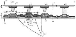
- FIG. 1 is a schematic view showing the structure of a color filter integrated transistor type liquid crystal panel according to an embodiment of the present invention.
- FIG. 2 is a flow chart showing the steps of a method of manufacturing a color filter integrated transistor type liquid crystal panel according to an embodiment of the present invention.
- FIG 3 is a schematic illustration of a UV-induced multi-region vertical alignment (UV 2 A) photoalignment technique.
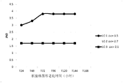
- Figure 4 is an image residual performance of the different liquid crystal formulations of Table 4.
- FIG. 1 is a schematic structural diagram of a color filter integrated transistor type liquid crystal panel 1 according to an embodiment of the invention.
- the color filter integrated transistor type liquid crystal panel 1 includes a first substrate 10, a second substrate 20, a liquid crystal layer 30, and a plurality of gap pillars 40.
- the first substrate 10 and the second substrate 20 are disposed opposite to each other, and the liquid crystal layer 30 is interposed between the first substrate 10 and the second substrate 20 .
- the first substrate 10 has a first alignment film (not shown) on its inner surface, and a second alignment film (not shown) on the inner surface of the second substrate 20.
- the liquid crystal layer 30 contacts the first alignment film and the second alignment film.
- the first substrate 10 includes a first transparent substrate 101, a thin film transistor array layer 102, a first protective layer 103, a color filter layer 104, a second protective layer 105, and a plurality of first transparent conductive films 106.
- the thin film transistor array layer 102 is disposed on an inner surface of the first transparent substrate 101.
- the first protective layer 103 is disposed on the thin film transistor array layer 102.
- the color filter layer 104 is disposed on the first protective layer 103.
- the second protective layer 105 is disposed on the color filter layer 104.
- the plurality of first transparent conductive films 106 are disposed on the second protective layer 105.
- the second substrate 20 includes a second transparent substrate 201, a black matrix layer 202, and a second transparent conductive film 203.
- the black matrix layer 202 is disposed on an inner surface of the second transparent substrate 201.
- the second transparent conductive film 203 is disposed on the black matrix layer 202.
- the plurality of gap pillars 40 are disposed between the color filter layer 104 and the black matrix layer 202.
- the liquid crystal layer 30 comprises at least one polar liquid crystal monomer and at least one non-polar liquid crystal monomer.
- the liquid crystal molecules of the liquid crystal layer 30 are negative liquid crystals, and the dielectric constant ( ⁇ ) of the liquid crystal molecules of the liquid crystal layer 30 is between -2.1 and -2.5 at 20 °C.
- the first and second alignment films composed of a polarization-sensitive material are formed by ultraviolet-induced multi-region vertical alignment (UV 2 A) photoalignment techniques.
- the polarized light sensitive material is a polyimide material having a reaction wavelength of 313 nm, and the alignment group of the polyimide material contains cinnamic acid and coumarin.
- FIG. 2 is a flow chart showing the steps of a method for manufacturing a color filter integrated transistor type liquid crystal panel 1 according to an embodiment of the present invention.
- the manufacturing method includes the following steps S11 to S14.
- a first substrate 10 is provided.
- the first substrate 10 includes a transparent substrate 101, a thin film transistor array layer 102 disposed on the transparent substrate 101, and a color filter layer 104 disposed on the thin film transistor array layer 102.
- step S12 a second substrate 20 is provided.
- a polarization-sensitive material is coated on the first substrate 10 and the second substrate 20, respectively, and then formed by ultraviolet-induced multi-region vertical alignment (UV 2 A) photoalignment technology.
- the polarized light sensitive material is a polyimide material having a reaction wavelength of 313 nm, and the alignment group of the polyimide material contains cinnamic acid and coumarin.
- a specific feature of the ultraviolet-induced multi-region vertical alignment (UV 2 A) photoalignment technique is that the ultraviolet polarized light is obliquely incident on an alignment film, and then the alignment film is along the incident direction of the ultraviolet polarized light. Dumping, that is, controlling the direction of alignment of the alignment film by controlling the direction of different incident light, thereby controlling the reversal of the liquid crystal, as shown in FIG.
- step S14 at least one polar liquid crystal monomer and at least one non-polar liquid crystal monomer are provided, and the polar liquid crystal monomer and the non-polar liquid crystal monomer are mixed, and then filled in the first
- a liquid crystal layer 30 is formed between a substrate 10 and the second substrate 20.
- the liquid crystal layer 30 contacts the first alignment film and the second alignment film.
- the liquid crystal molecules of the liquid crystal layer 30 are negative liquid crystals, and the dielectric constant ( ⁇ ) of the liquid crystal molecules of the liquid crystal layer is between -2.1 and -2.5 at 20 °C.
- the color filter integrated transistor type liquid crystal panel of the present invention can be fabricated.
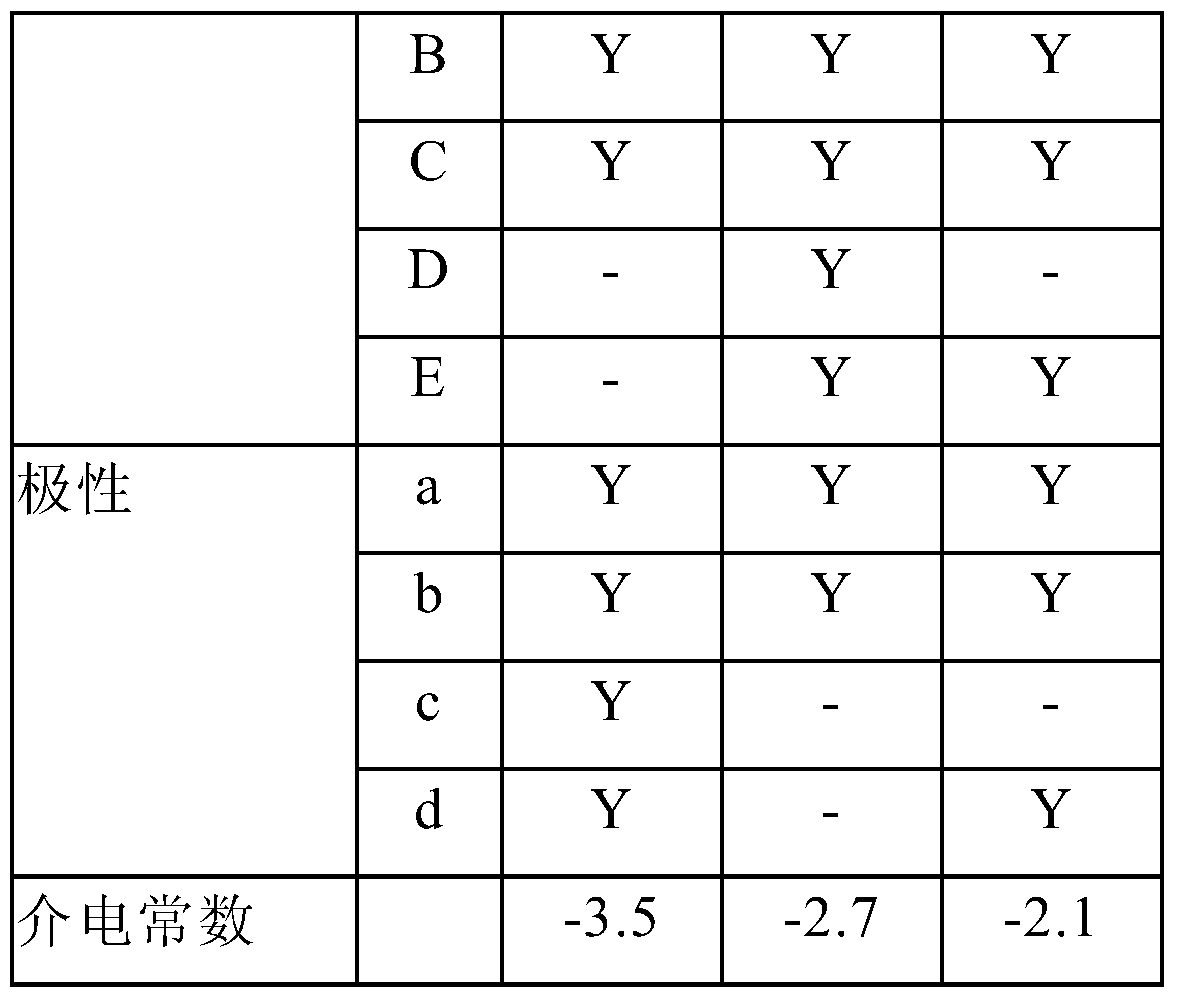
- Table 1 is a dielectric constant ( ⁇ ) of different liquid crystal formulations in a specific example of the present invention.
- the dielectric constant (??) of the liquid crystal mixture LC-1 having the monomers A to C and the monomers a to d was -3.5.
- the dielectric constant (??) of the liquid crystal mixture LC-2 having the monomers A to E and the monomers a to b was -2.7.
- the dielectric constant (??) of the liquid crystal mixture LC-3 having the monomers A to C and E and the monomers a to b and d was -2.1.
- dielectric constants (??) can be obtained by adjustment of the liquid crystal formulation (i.e., selection of different polar liquid crystal monomers and different non-polar liquid crystal monomers).
- the dielectric constant (??) can be controlled by adjusting the content of the monomer.
- FIG. 4 is an image residual performance of different liquid crystal formulations of Table 4.
- JND is represented by JND at different times.
- JND is indicated by 1.7 in time, which is the best.
- the larger the JND value the worse the image residual performance.
- ⁇ dielectric constant
- ?? dielectric constant
- the color filter integrated transistor type liquid crystal panel of the present invention and the method of fabricating the same are formed by forming a color filter integrated transistor type liquid crystal panel by ultraviolet-induced multi-region vertical alignment (UV 2 A) photoalignment technique. Improving the image residual of the existing color filter integrated transistor type liquid crystal display by controlling the dielectric constant ( ⁇ ) of the liquid crystal molecules of the liquid crystal layer in the transistor liquid crystal panel by controlling the color filter The problem.
- UV 2 A ultraviolet-induced multi-region vertical alignment
Landscapes
- Physics & Mathematics (AREA)
- Nonlinear Science (AREA)
- Chemical & Material Sciences (AREA)
- Crystallography & Structural Chemistry (AREA)
- General Physics & Mathematics (AREA)
- Optics & Photonics (AREA)
- Mathematical Physics (AREA)
- Spectroscopy & Molecular Physics (AREA)
- Engineering & Computer Science (AREA)
- Manufacturing & Machinery (AREA)
- Liquid Crystal (AREA)
Abstract
一种彩色滤光片整合晶体管式(COA)液晶面板(1)及其制造方法,其是通过以紫外线诱导多区域垂直配向(UV 2A)的光配向技术形成COA液晶面板(1)中的配向膜,以及通过控制COA液晶面板(1)中液晶层(30)的液晶分子的介电常数(△ε),来改进现有COA液晶显示器的影像残留的问题。
Description
本发明是有关于一种液晶面板及其制造方法,特别是有关于一种彩色滤光片整合晶体管式(Color filter on Array,COA)液晶面板及其制造方法。
彩色滤光片整合晶体管式(COA)液晶显示器是一种将彩色滤光片与薄膜晶体管阵列设置于同一基板的液晶显示器,其可以有效的提高开口率,还能解决大尺寸面板的对准问题,且同时降低由照光产生的漏电流,因此彩色滤光片整合晶体管技术特别适用于大尺寸面板的显示器。
然而,由于现在很多研究机构为了提高COA液晶显示器的响应时间等光学性能,会将所述COA液晶显示器中的液晶层的液晶分子的介电常数设计的很高(介电常数的提高主要是通过极性液晶单体的比例增加,但是极性液晶单体增加后会导致液晶的稳定性降低),因此容易使得液晶在使用过程中发生劣化,而产生可移动离子,使电压保持率(VHR)等降低,从而导致信赖性(尤其是影像残留)不佳。
因此,有必要提供一种可以改进影像残留的彩色滤光片整合晶体管式液晶面板,来解决现有技术所存在的问题。
发明内容
本发明的主要目的在于提供一种彩色滤光片整合晶体管式(COA)液晶面板及其制造方法。通过以紫外线诱导多区域垂直配向(Ultraviolet induced multi-domain vertical alignment,UV2A)的光配向技术形成所述彩色滤光片整合晶体管式液晶面板中的配向膜,以及通过控制所述彩色滤光片整合晶体管式液晶面板中液晶层的液晶分子的介电常数(△ε),来改进现有彩色滤光片整合晶体管式液晶显示器的影像残留的问题。
为达成本发明的前述目的,本发明提供一种彩色滤光片整合晶体管式液晶面板,包含:
一第一基板,具有一第一配向膜,所述第一基板包含:
一透明基板;
一薄膜晶体管阵列层,设置于所述透明基板上;以及
一彩色滤光层,设置于所述薄膜晶体管阵列层上;
一第二基板,具有一第二配向膜,所述第一基板与第二基板相对设置;以及
一液晶层,夹设于所述第一基板与所述第二基板之间,且所述液晶层接触所述第一配向膜和所述第二配向膜,所述液晶层包含至少一种极性液晶单体和至少一种非极性液晶单体。由一偏振光敏感材料构成的所述第一及第二配向膜是通过紫外线诱导多区域垂直配向(UV2A)的光配向技术而形成的。
在本发明的一实施例中,所述液晶层的液晶分子为负性液晶。
在本发明的一实施例中,所述液晶层的液晶分子的介电常数(△ε)在20℃下是介于-2.1~-2.5之间。
在本发明的一实施例中,所述偏振光敏感材料为聚酰亚胺材料。
在本发明的一实施例中,所述聚酰亚胺材料的反应波长为313nm。
在本发明的一实施例中,所述聚酰亚胺材料的配向基团包含肉桂酸、香豆素。
再者,本发明另提供一种彩色滤光片整合晶体管式液晶面板的制造方法,包括以下步骤:
提供一第一基板,所述第一基板包含一透明基板、一设置于所述透明基板上的薄膜晶体管阵列层及一设置于所述薄膜晶体管阵列层上的彩色滤光层;
提供一第二基板;
分别涂布一偏振光敏感材料在所述第一基板及所述第二基板上,而后通过紫外线诱导多区域垂直配向(UV2A)的光配向技术来相应地形成一第一配向膜
及一第二配向膜;以及
提供至少一种极性液晶单体和至少一种非极性液晶单体,且混合所述极性液晶单体及所述非极性液晶单体,而后填充在所述第一基板及所述第二基板之间,形成一液晶层,所述液晶层接触所述第一配向膜和所述第二配向膜。
在本发明的一实施例中,所述液晶层的液晶分子为负性液晶。
在本发明的一实施例中,所述液晶层的液晶分子的介电常数(△ε)在20℃下是介于-2.1~-2.5之间。
在本发明的一实施例中,所述偏振光敏感材料为聚酰亚胺材料。
在本发明的一实施例中,所述聚酰亚胺材料的反应波长为313nm。
在本发明的一实施例中,所述聚酰亚胺材料的配向基团包含肉桂酸、香豆素。
本发明与现有技术相比具有明显的优点和有益的效果。通过上述技术方案,本发明彩色滤光片整合晶体管式液晶面板及其制造方法至少具有下列优点及有益效果:通过以紫外线诱导多区域垂直配向(UV2A)的光配向技术形成所述彩色滤光片整合晶体管式液晶面板中的配向膜,以及通过控制所述彩色滤光片整合晶体管式液晶面板中液晶层的液晶分子的介电常数(△ε),来改进现有彩色滤光片整合晶体管式液晶显示器的影像残留的问题。
图1是本发明一实施例中彩色滤光片整合晶体管式液晶面板的构造示意图。
图2是本发明一实施例中彩色滤光片整合晶体管式液晶面板的制造方法的步骤流程图。
图3是紫外线诱导多区域垂直配向(UV2A)的光配向技术的示意图。
图4是表4的不同液晶配方的影像残留表现。
1 COA液晶面板 202 黑色矩阵层
10 第一基板 203 第二透明导电膜
20 第二基板 1021 Mo/Al
30 液晶层 1022 G-SiNx
40 间隙柱 1023 a-Si
50 框胶 1024 MoN/Al/Mo
101 第一透明基板、透明基板 R 红色子像素
102 薄膜晶体管阵列层 G 绿色子像素
103 第一保护层 B 蓝色子像素
104 彩色滤光层 D1 段差
105 第二保护层 D2 间隙柱差
106 第一透明导电膜 D3 B&RG膜厚差
201 第二透明基板 S11-S14 步骤
为更进一步阐述本发明为达成预订发明目的所采取的技术手段及功效,以下结合附图及较佳实施例,对依据本发明提出的彩色滤光片整合晶体管式液晶面板及其制造方法其具体实施方式、结构、特征及其功效,详细说明如后。
请参照图1,其为本发明一实施例中彩色滤光片整合晶体管式液晶面板1的构造示意图。所述彩色滤光片整合晶体管式液晶面板1包含一第一基板10、一第二基板20、一液晶层30及若干间隙柱40。所述第一基板10与第二基板20相对设置,且所述液晶层30夹设于所述第一基板10与第二基板20之间。所述第一基板10的内表面上具有一第一配向膜(图中未示出),所述第二基板20的内表面上具有一第二配向膜(图中未示出)。所述液晶层30接触所述第一配向膜及所述第二配向膜。
所述第一基板10包括一第一透明基板101、一薄膜晶体管阵列层102、一第一保护层103、一彩色滤光层104、一第二保护层105及若干第一透明导电膜106。所述薄膜晶体管阵列层102是设置于所述第一透明基板101的内表面上。所述第一保护层103是设置于所述薄膜晶体管阵列层102上。所述彩色滤光层104是设置于所述第一保护层103上。所述第二保护层105是设置于所述彩色滤光层104上。所述若干第一透明导电膜106是设置于所述第二保护层105上。
所述第二基板20包括一第二透明基板201、一黑色矩阵层202及一第二透明导电膜203。所述黑色矩阵层202是设置于所述第二透明基板201的内表面上。所述第二透明导电膜203是设置于所述黑色矩阵层202上。所述若干间隙柱40是设置于所述彩色滤光层104及所述黑色矩阵层202之间。
所述液晶层30包含至少一种极性液晶单体和至少一种非极性液晶单体。所述液晶层30的液晶分子为负性液晶,并且所述液晶层30的液晶分子的介电常数(△ε)在20℃下是介于-2.1~-2.5之间。
由一偏振光敏感材料构成的所述第一及第二配向膜是通过紫外线诱导多区域垂直配向(UV2A)的光配向技术而形成的。所述偏振光敏感材料是一反应波长为313nm的聚酰亚胺材料,且所述聚酰亚胺材料的配向基团包含肉桂酸、香豆素。
请参照图2,其为本发明一实施例中彩色滤光片整合晶体管式液晶面板1的制造方法的步骤流程图,该制造方法包括下述步骤S11至S14。
在步骤S11中,提供一第一基板10。所述第一基板10包含一透明基板101、一设置于所述透明基板101上的薄膜晶体管阵列层102及一设置于所述薄膜晶体管阵列层102上的彩色滤光层104。
在步骤S12中,提供一第二基板20。
在步骤S13中,分别涂布一偏振光敏感材料在所述第一基板10及所述
第二基板20上,而后通过紫外线诱导多区域垂直配向(UV2A)的光配向技术来相应地形成一第一配向膜及一第二配向膜(图中未示出)。所述偏振光敏感材料是一反应波长为313nm的聚酰亚胺材料,且所述聚酰亚胺材料的配向基团包含肉桂酸、香豆素。所述紫外线诱导多区域垂直配向(UV2A)的光配向技术的具体特征为,紫外偏振光为倾斜入射至一配向膜,然后所述配向膜会沿着所述紫外偏振光的入射方向而倾倒,亦即,可以通过控制不同的入射光的方向,来控制配向膜的配向方向,从而控制液晶的倒向,如图3所示。
在步骤S14中,提供至少一种极性液晶单体和至少一种非极性液晶单体,且混合所述极性液晶单体及所述非极性液晶单体,而后填充在所述第一基板10及所述第二基板20之间,形成一液晶层30。所述液晶层30接触所述第一配向膜和所述第二配向膜。所述液晶层30的液晶分子为负性液晶,且所述液晶层的液晶分子的介电常数(△ε)在20℃下是介于-2.1~-2.5之间。
通过执行上述步骤S11至S14,即可制作出本发明的彩色滤光片整合晶体管式液晶面板。
请参照表1,其是本发明的具体实例中不同液晶配方的介电常数(△ε)。具有单体A~C和单体a~d的液晶混合物LC-1的介电常数(△ε)为-3.5。具有单体A~E和单体a~b的液晶混合物LC-2的介电常数(△ε)为-2.7。具有单体A~C及E和单体a~b及d的液晶混合物LC-3的介电常数(△ε)为-2.1。因此,可以得知,通过液晶配方的调整(亦即,不同的极性液晶单体和不同的非极性液晶单体的选取),可以获得不同的介电常数(△ε)。另外,也可通过调整单体的含量来控制其介电常数(△ε)。
[表1]

接着,请参照图4,其是表4的不同液晶配方的影像残留表现。在此,以不同时间的JND表示。JND无时以1.7表示,其是最佳。JND数值越大,影像残留表现越差。从图4中可以看出随着介电常数(△ε)变大,影像残留表现越来越好。因此,可以得知,通过控制液晶的介电常数(△ε)可以改善液晶的影像残留表现。
如上所述,本发明的彩色滤光片整合晶体管式液晶面板及其制造方法是通过以紫外线诱导多区域垂直配向(UV2A)的光配向技术形成所述彩色滤光片整合晶体管式液晶面板中的配向膜,以及通过控制所述彩色滤光片整合晶体管式液晶面板中液晶层的液晶分子的介电常数(△ε),来改进现有彩色滤光片整合晶体管式液晶显示器的影像残留的问题。
本发明已由上述相关实施例加以描述,然而上述实施例仅为实施本发明的范例。必需指出的是,已公开的实施例并未限制本发明的范围。相反地,包含于权利要求书的精神及范围的修改及均等设置均包括于本发明的范围内。
Claims (16)
- 一种彩色滤光片整合晶体管式(Color filter on Array,COA)液晶面板,包含:一第一基板,具有一第一配向膜,所述第一基板包含:一透明基板;一薄膜晶体管阵列层,设置于所述透明基板上;以及一彩色滤光层,设置于所述薄膜晶体管阵列层上;一第二基板,具有一第二配向膜,所述第一基板与第二基板相对设置;以及一液晶层,夹设于所述第一基板与所述第二基板之间,且所述液晶层接触所述第一配向膜和所述第二配向膜,所述液晶层包含至少一种极性液晶单体和至少一种非极性液晶单体,所述液晶层的液晶分子为负性液晶,所述液晶层的液晶分子的介电常数(△ε)在20℃下是介于-2.1~-2.5之间,其中由一偏振光敏感材料构成的所述第一及第二配向膜是通过紫外线诱导多区域垂直配向(Ultraviolet induced multi-domain vertical alignment,UV2A)的光配向技术而形成的。
- 根据权利要求1所述的彩色滤光片整合晶体管式液晶面板,其中所述偏振光敏感材料为聚酰亚胺材料。
- 根据权利要求2所述的彩色滤光片整合晶体管式液晶面板,其中所述聚酰亚胺材料的反应波长为313nm。
- 根据权利要求2所述的彩色滤光片整合晶体管式液晶面板,其中所述聚酰亚胺材料的配向基团包含肉桂酸、香豆素。
- 一种彩色滤光片整合晶体管式(Color filter on Array,COA)液晶面板,包含:一第一基板,具有一第一配向膜,所述第一基板包含:一透明基板;一薄膜晶体管阵列层,设置于所述透明基板上;以及一彩色滤光层,设置于所述薄膜晶体管阵列层上;一第二基板,具有一第二配向膜,所述第一基板与第二基板相对设置;以及一液晶层,夹设于所述第一基板与所述第二基板之间,且所述液晶层接触所述第一配向膜和所述第二配向膜,所述液晶层包含至少一种极性液晶单体和至少一种非极性液晶单体,其中由一偏振光敏感材料构成的所述第一及第二配向膜是通过紫外线诱导多区域垂直配向(Ultraviolet induced multi-domain vertical alignment,UV2A)的光配向技术而形成的。
- 根据权利要求5所述的彩色滤光片整合晶体管式液晶面板,其中所述液晶层的液晶分子为负性液晶。
- 根据权利要求6所述的彩色滤光片整合晶体管式液晶面板,其中所述液晶层的液晶分子的介电常数(△ε)在20℃下是介于-2.1~-2.5之间。
- 根据权利要求5所述的彩色滤光片整合晶体管式液晶面板,其中所述偏振光敏感材料为聚酰亚胺材料。
- 根据权利要求8所述的彩色滤光片整合晶体管式液晶面板,其中所述聚酰亚胺材料的反应波长为313nm。
- 根据权利要求8所述的彩色滤光片整合晶体管式液晶面板,其中所述聚酰亚胺材料的配向基团包含肉桂酸、香豆素。
- 一种彩色滤光片整合晶体管式(Color filter on Array,COA)液晶面板的制造方法,包括以下步骤:提供一第一基板,所述第一基板包含一透明基板、一设置于所述透明基板上的薄膜晶体管阵列层及一设置于所述薄膜晶体管阵列层上的彩色滤光层;提供一第二基板;分别涂布一偏振光敏感材料在所述第一基板及所述第二基板上,而后通过紫 外线诱导多区域垂直配向(Ultraviolet induced multi-domain vertical alignment,UV2A)的光配向技术来相应地形成一第一配向膜及一第二配向膜;以及提供至少一种极性液晶单体和至少一种非极性液晶单体,且混合所述极性液晶单体及所述非极性液晶单体,而后填充在所述第一基板及所述第二基板之间,形成一液晶层,所述液晶层接触所述第一配向膜和所述第二配向膜。
- 根据权利要求11所述的彩色滤光片整合晶体管式液晶面板的制造方法,其中所述液晶层的液晶分子为负性液晶。
- 根据权利要求12所述的彩色滤光片整合晶体管式液晶面板的制造方法,其中所述液晶层的液晶分子的介电常数(△ε)在20℃下是介于-2.1~-2.5之间。
- 根据权利要求11所述的彩色滤光片整合晶体管式液晶面板的制造方法,其中所述偏振光敏感材料为聚酰亚胺材料。
- 根据权利要求14所述的彩色滤光片整合晶体管式液晶面板的制造方法,其中所述聚酰亚胺材料的反应波长为313nm。
- 根据权利要求14所述的彩色滤光片整合晶体管式液晶面板的制造方法,其中所述聚酰亚胺材料的配向基团包含肉桂酸、香豆素。
Priority Applications (1)
| Application Number | Priority Date | Filing Date | Title |
|---|---|---|---|
| US14/778,745 US10216030B2 (en) | 2015-07-17 | 2015-08-07 | Color filter on array type liquid crystal panel and manufacturing method for the same |
Applications Claiming Priority (2)
| Application Number | Priority Date | Filing Date | Title |
|---|---|---|---|
| CN201510422650.X | 2015-07-17 | ||
| CN201510422650.XA CN105093689A (zh) | 2015-07-17 | 2015-07-17 | 彩色滤光片整合晶体管式液晶面板及其制造方法 |
Publications (1)
| Publication Number | Publication Date |
|---|---|
| WO2017012151A1 true WO2017012151A1 (zh) | 2017-01-26 |
Family
ID=54574461
Family Applications (1)
| Application Number | Title | Priority Date | Filing Date |
|---|---|---|---|
| PCT/CN2015/086355 Ceased WO2017012151A1 (zh) | 2015-07-17 | 2015-08-07 | 彩色滤光片整合晶体管式液晶面板及其制造方法 |
Country Status (3)
| Country | Link |
|---|---|
| US (1) | US10216030B2 (zh) |
| CN (1) | CN105093689A (zh) |
| WO (1) | WO2017012151A1 (zh) |
Families Citing this family (3)
| Publication number | Priority date | Publication date | Assignee | Title |
|---|---|---|---|---|
| CN104991376A (zh) | 2015-07-29 | 2015-10-21 | 深圳市华星光电技术有限公司 | 液晶显示器及其液晶面板 |
| CN106773351A (zh) * | 2016-12-29 | 2017-05-31 | 惠科股份有限公司 | 一种显示面板和显示装置 |
| CN109116615A (zh) * | 2018-08-20 | 2019-01-01 | 深圳市华星光电技术有限公司 | 彩膜基板及液晶面板 |
Citations (5)
| Publication number | Priority date | Publication date | Assignee | Title |
|---|---|---|---|---|
| US20030160923A1 (en) * | 2002-02-19 | 2003-08-28 | Yao-Dong Ma | Full color cholesteric displays employing cholesteric color filter |
| US20040183979A1 (en) * | 2003-03-19 | 2004-09-23 | Cheuh-Ju Chen | In-plane switching liquid crystal display and method for manufacturing the same |
| US7081935B2 (en) * | 2001-08-01 | 2006-07-25 | Sharp Kabushiki Kaisha | Liquid crystal display device with alignment layer including a diamine component and treated by UV irradiation |
| CN202141877U (zh) * | 2011-07-12 | 2012-02-08 | 北京京东方光电科技有限公司 | 一种液晶显示面板 |
| CN104777673A (zh) * | 2015-04-24 | 2015-07-15 | 深圳市华星光电技术有限公司 | 显示面板及其制造方法 |
Family Cites Families (11)
| Publication number | Priority date | Publication date | Assignee | Title |
|---|---|---|---|---|
| TWI438525B (zh) * | 2010-07-19 | 2014-05-21 | Au Optronics Corp | 顯示面板 |
| US9405153B2 (en) * | 2011-08-25 | 2016-08-02 | Sharp Kabushiki Kaisha | Method for manufacturing liquid crystal display device |
| KR101820966B1 (ko) | 2011-10-20 | 2018-01-23 | 삼성디스플레이 주식회사 | 액정표시장치, 배향막 및 이들을 제조하는 방법들 |
| JP5850283B2 (ja) * | 2013-06-17 | 2016-02-03 | Dic株式会社 | ネマチック液晶組成物及びこれを用いた液晶表示素子 |
| CN103525429B (zh) * | 2013-08-30 | 2016-02-24 | 晶美晟光电材料(南京)有限公司 | 液晶化合物、其制备方法、包括其的液晶混合物和应用 |
| WO2015064629A1 (ja) * | 2013-10-30 | 2015-05-07 | Dic株式会社 | 液晶表示素子 |
| CN104730770A (zh) * | 2013-12-24 | 2015-06-24 | 群创光电股份有限公司 | 液晶显示设备 |
| US10344211B2 (en) * | 2014-12-18 | 2019-07-09 | Dic Corporation | Liquid crystal composition and liquid crystal display element using same |
| CN104777672A (zh) * | 2015-04-24 | 2015-07-15 | 深圳市华星光电技术有限公司 | 显示面板及其制造方法 |
| CN105204231B (zh) * | 2015-10-13 | 2019-02-22 | 深圳市华星光电技术有限公司 | 液晶面板及其制造方法 |
| CN106154630B (zh) * | 2016-08-31 | 2019-07-12 | 深圳市华星光电技术有限公司 | 一种coa型液晶面板及制作方法 |
-
2015
- 2015-07-17 CN CN201510422650.XA patent/CN105093689A/zh active Pending
- 2015-08-07 WO PCT/CN2015/086355 patent/WO2017012151A1/zh not_active Ceased
- 2015-08-07 US US14/778,745 patent/US10216030B2/en active Active
Patent Citations (5)
| Publication number | Priority date | Publication date | Assignee | Title |
|---|---|---|---|---|
| US7081935B2 (en) * | 2001-08-01 | 2006-07-25 | Sharp Kabushiki Kaisha | Liquid crystal display device with alignment layer including a diamine component and treated by UV irradiation |
| US20030160923A1 (en) * | 2002-02-19 | 2003-08-28 | Yao-Dong Ma | Full color cholesteric displays employing cholesteric color filter |
| US20040183979A1 (en) * | 2003-03-19 | 2004-09-23 | Cheuh-Ju Chen | In-plane switching liquid crystal display and method for manufacturing the same |
| CN202141877U (zh) * | 2011-07-12 | 2012-02-08 | 北京京东方光电科技有限公司 | 一种液晶显示面板 |
| CN104777673A (zh) * | 2015-04-24 | 2015-07-15 | 深圳市华星光电技术有限公司 | 显示面板及其制造方法 |
Also Published As
| Publication number | Publication date |
|---|---|
| US10216030B2 (en) | 2019-02-26 |
| CN105093689A (zh) | 2015-11-25 |
| US20180120629A1 (en) | 2018-05-03 |
Similar Documents
| Publication | Publication Date | Title |
|---|---|---|
| US8619228B2 (en) | Liquid crystal display device and manufacturing method | |
| CN101435961B (zh) | Tft-lcd彩膜/阵列基板、液晶显示面板及其制造方法 | |
| US9880421B2 (en) | Curved liquid crystal display | |
| US20180180947A1 (en) | Liquid crystal display device and manufacturing method thereof | |
| CN105974636A (zh) | 液晶显示面板的制作方法 | |
| CN105404047A (zh) | Coa型液晶显示面板的制作方法及coa型液晶显示面板 | |
| US9612464B2 (en) | Liquid crystal display | |
| TW201224613A (en) | Crystal display substrate and crystal display device | |
| US20180335553A1 (en) | Method for manufacturing color filter substrate and method for manufacturing liquid crystal panel | |
| JP2011237571A (ja) | 液晶表示装置 | |
| CN106324880A (zh) | 液晶基板的制作方法 | |
| TW201248275A (en) | Liquid crystal display panel and method for fabricating the same | |
| US10197845B2 (en) | Manufacturing method of color filter substrate and manufacturing method of liquid crystal panel | |
| WO2016176882A1 (zh) | 彩色滤光片及其制作方法、液晶显示面板 | |
| WO2015070477A1 (zh) | 液晶显示面板及液晶显示器 | |
| CN108153040A (zh) | 黑色矩阵与间隔物的制作方法 | |
| WO2017012151A1 (zh) | 彩色滤光片整合晶体管式液晶面板及其制造方法 | |
| JP5981100B2 (ja) | スイッチング素子基板 | |
| CN102135678A (zh) | 彩色滤光片及其制造方法、液晶显示装置 | |
| US10114251B2 (en) | Liquid crystal display having holding member and method of fabricating same | |
| TWI625576B (zh) | Liquid crystal display device | |
| US10365518B2 (en) | Methods for manufacturing display panel and display apparatus | |
| US9366932B2 (en) | TFT-LCD array substrate manufacturing method and LCD panel/device produced by the same | |
| US20080174723A1 (en) | Liquid crystal display device and manufacturing method thereof | |
| US20150253628A1 (en) | Liquid crystal display device, method of manufacturing the same, and alignment layer composition |
Legal Events
| Date | Code | Title | Description |
|---|---|---|---|
| WWE | Wipo information: entry into national phase |
Ref document number: 14778745 Country of ref document: US |
|
| 121 | Ep: the epo has been informed by wipo that ep was designated in this application |
Ref document number: 15898707 Country of ref document: EP Kind code of ref document: A1 |
|
| NENP | Non-entry into the national phase |
Ref country code: DE |
|
| 122 | Ep: pct application non-entry in european phase |
Ref document number: 15898707 Country of ref document: EP Kind code of ref document: A1 |