WO2017010260A1 - 固体撮像素子および駆動方法、並びに電子機器 - Google Patents
固体撮像素子および駆動方法、並びに電子機器 Download PDFInfo
- Publication number
- WO2017010260A1 WO2017010260A1 PCT/JP2016/068780 JP2016068780W WO2017010260A1 WO 2017010260 A1 WO2017010260 A1 WO 2017010260A1 JP 2016068780 W JP2016068780 W JP 2016068780W WO 2017010260 A1 WO2017010260 A1 WO 2017010260A1
- Authority
- WO
- WIPO (PCT)
- Prior art keywords
- unit
- diffusion region
- photoelectric conversion
- signal
- charge
- Prior art date
- Legal status (The legal status is an assumption and is not a legal conclusion. Google has not performed a legal analysis and makes no representation as to the accuracy of the status listed.)
- Ceased
Links
Images







Classifications
-
- H—ELECTRICITY
- H04—ELECTRIC COMMUNICATION TECHNIQUE
- H04N—PICTORIAL COMMUNICATION, e.g. TELEVISION
- H04N25/00—Circuitry of solid-state image sensors [SSIS]; Control thereof
- H04N25/40—Extracting pixel data from image sensors by controlling scanning circuits, e.g. by modifying the number of pixels sampled or to be sampled
-
- H—ELECTRICITY
- H04—ELECTRIC COMMUNICATION TECHNIQUE
- H04N—PICTORIAL COMMUNICATION, e.g. TELEVISION
- H04N25/00—Circuitry of solid-state image sensors [SSIS]; Control thereof
- H04N25/70—SSIS architectures; Circuits associated therewith
- H04N25/76—Addressed sensors, e.g. MOS or CMOS sensors
-
- H—ELECTRICITY
- H04—ELECTRIC COMMUNICATION TECHNIQUE
- H04N—PICTORIAL COMMUNICATION, e.g. TELEVISION
- H04N25/00—Circuitry of solid-state image sensors [SSIS]; Control thereof
- H04N25/70—SSIS architectures; Circuits associated therewith
- H04N25/76—Addressed sensors, e.g. MOS or CMOS sensors
- H04N25/77—Pixel circuitry, e.g. memories, A/D converters, pixel amplifiers, shared circuits or shared components
Definitions
- the present technology relates to a solid-state imaging device, a driving method, and an electronic device, and more particularly, to a solid-state imaging device, a driving method, and an electronic device that can obtain a higher quality image.
- each pixel photoelectrically converts received light, accumulates the obtained charge, a charge transfer unit that transfers the charge accumulated in the photoelectric conversion unit, and a charge transfer And an FD (Floating Diffusion) unit for accumulating the charges transferred from the photoelectric conversion unit via the unit. Then, a signal corresponding to the electric charge accumulated in the FD unit is output to the vertical signal line through an amplification transistor or the like.
- a charge transfer unit that transfers the charge accumulated in the photoelectric conversion unit
- FD Floating Diffusion
- an additional capacitor is connected to the FD unit via a connection switch, and the FD unit and the additional capacitor are electrically connected by the connection switch as necessary.
- the conversion efficiency is lowered. Conversely, if the charge obtained by the photoelectric conversion unit is accumulated only in the FD unit and the charge is read out as a signal, the conversion efficiency increases.
- the maximum signal amount is subject to restrictions on the range of voltage values that can be detected by an AD (Analog-Digital) converter downstream of the vertical signal line and the capacity of the FD unit.
- AD Analog-Digital
- the FD unit and the additional capacitor are electrically connected and charges are accumulated in the FD unit and the additional capacitor, and when the signal is read, the SNR ( Signal to Noise Ratio) gets worse.
- the FD section and additional capacitance are electrically connected when large signals are used to reduce conversion efficiency, and when small signals are used, the FD section and additional capacitors are electrically disconnected to increase conversion efficiency, thereby increasing the signal volume. To deal with both the constraints and the worsening of noise.
- a connection switch is provided between the FD portion in the pixel and the FD portion in the pixel adjacent to the pixel.
- connection switch when the connection switch is turned on and the two FD units are connected, the charge obtained in the photoelectric conversion unit of one pixel is stored in the connected FD unit and the signal is read out. Efficiency can be lowered. On the contrary, when the connection switch is turned off to store the charge obtained in the photoelectric conversion unit in the pixel only in the FD unit in the pixel and read out the signal, the conversion efficiency can be increased.
- connection switch that connects the FD unit and the additional capacitor described above and the connection switch that connects the FD unit between adjacent pixels.
- connection switch When the connection switch is in an off state, that is, in a non-conducting state, the parasitic capacitance does not fluctuate so much that the signal reading is not particularly affected.
- connection switch when the connection switch is in the on state, that is, in the conductive state, the parasitic capacitance greatly varies depending on the voltage between the gate and the source of the connection switch. Since the FD unit is connected to the connection switch, a parasitic capacitance is added to the capacitance of the FD unit.
- the total capacity of the FD portion to which parasitic capacitance is added varies depending on the amount of charge obtained in the photoelectric conversion unit, and the amount of charge obtained in the photoelectric conversion unit and the pixel depending on the charge
- the linearity (linearity) with the read signal is deteriorated. That is, the signal read from the pixel changes non-linearly with respect to the amount of change in charge obtained by the photoelectric conversion unit.
- the present technology has been made in view of such a situation, and makes it possible to obtain a higher quality image.
- the solid-state imaging device includes a photoelectric conversion unit that photoelectrically converts incident light, a first diffusion region that accumulates charges obtained by the photoelectric conversion, and a first diffusion region.
- a first readout unit that outputs a signal corresponding to the accumulated charge; a second diffusion region that is connected to the first diffusion region and accumulates charge; the first diffusion region; and the second diffusion region.
- a first connection switch provided between the diffusion region and electrically connecting the first diffusion region and the second diffusion region; and according to a charge accumulated in the second diffusion region
- a second readout unit that outputs a signal, and the first connection switch is controlled to electrically connect the first diffusion region and the second diffusion region, and obtained by the photoelectric conversion.
- the first connection switch is controlled to electrically separate the first diffusion region and the second diffusion region, and a signal corresponding to the charge accumulated in the first diffusion region is transmitted to the first diffusion region.
- a control unit for outputting a signal corresponding to the electric charge accumulated in the second diffusion region from the second reading unit.
- the first reading unit and the second reading unit can output a signal corresponding to the charge to the same vertical signal line.
- the first reading unit and the second reading unit can output signals corresponding to the charges to different vertical signal lines.
- the solid-state imaging device may further include an adding unit that adds the signal output from the first reading unit and the signal output from the second reading unit.
- the photoelectric conversion unit, the first diffusion region, and the first readout unit are provided in a predetermined pixel, and the second diffusion region and the second readout unit are different from the predetermined pixel. Can be provided.
- a plurality of the photoelectric conversion units can be connected to the first diffusion region.
- the solid-state imaging device is connected to the second diffusion region and is provided between the second diffusion region and the third diffusion region, and is provided between the second diffusion region and the third diffusion region. And a second connection switch for electrically connecting the third diffusion region and the third diffusion region.
- the driving method includes a photoelectric conversion unit that photoelectrically converts incident light, a first diffusion region that accumulates charges obtained by the photoelectric conversion, and accumulation in the first diffusion region.
- a first readout unit that outputs a signal corresponding to the generated charge, a second diffusion region that is connected to the first diffusion region and stores the charge, the first diffusion region, and the second diffusion
- a connection switch that is provided between the first diffusion region and the second diffusion region, and outputs a signal corresponding to the charge accumulated in the second diffusion region.
- a method of driving a solid-state imaging device including a second readout unit, wherein the photoelectric conversion is performed by controlling the connection switch to electrically connect the first diffusion region and the second diffusion region.
- the electric charge obtained by the first diffusion region and the second A signal corresponding to the electric charge accumulated in the first diffusion region is stored in the diffusion region, and the connection switch is controlled to electrically separate the first diffusion region and the second diffusion region. Are output from the first readout unit, and a signal corresponding to the charge accumulated in the second diffusion region is output from the second readout unit.
- a photoelectric conversion unit that photoelectrically converts incident light, a first diffusion region that accumulates charges obtained by the photoelectric conversion, and a first diffusion region that is accumulated in the first diffusion region
- a first readout unit that outputs a signal corresponding to an electric charge
- a second diffusion region that is connected to the first diffusion region and accumulates charge
- the first diffusion region and the second diffusion region A connection switch that electrically connects the first diffusion region and the second diffusion region, and a second signal that outputs a signal corresponding to the charge accumulated in the second diffusion region.
- connection switch is controlled to electrically connect the first diffusion region and the second diffusion region, and the charge obtained by the photoelectric conversion is In the first diffusion region and the second diffusion region
- connection switch is controlled to electrically isolate the first diffusion region and the second diffusion region, and a signal corresponding to the charge accumulated in the first diffusion region is transmitted to the first diffusion region.
- a signal corresponding to the electric charge accumulated in the second diffusion region is output from the second reading unit.
- the electronic device according to the second aspect of the present technology has the same configuration as the solid-state imaging device according to the first aspect of the present technology.
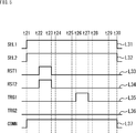
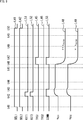
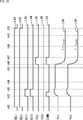
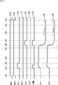
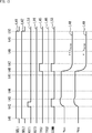
- 6 is a timing chart illustrating a pixel driving method. It is a figure explaining a parasitic capacitance. It is a figure explaining a pixel structure. 6 is a timing chart illustrating a pixel driving method. It is a figure which shows the structural example of the solid-state image sensor to which this technique is applied. It is a figure explaining a pixel structure. 6 is a timing chart illustrating a pixel driving method. 6 is a timing chart illustrating a pixel driving method. 6 is a timing chart illustrating a pixel driving method. 6 is a timing chart illustrating a pixel driving method. 6 is a timing chart illustrating a pixel driving method. 6 is a timing chart illustrating a pixel driving method. 6 is a timing chart illustrating a pixel driving method.
- 6 is a timing chart illustrating a pixel driving method. 6 is a timing chart illustrating a pixel driving method. It is a figure explaining other examples of pixel composition. It is a figure explaining other examples of pixel composition. It is a figure explaining other examples of pixel composition. It is a figure explaining other examples of pixel composition. It is a figure which shows the structural example of an imaging device. It is a figure which shows the usage example which uses a solid-state image sensor.
- the present technology relates to a solid-state imaging device that can improve the linearity at the time of signal readout and obtain a higher quality image by suppressing the capacitance value fluctuation of the FD unit to be small.
- the general configuration of the pixels of the solid-state imaging device that can change the conversion efficiency is the configuration shown in FIG.
- a photoelectric conversion unit 21 is provided with a photoelectric conversion unit 21, a charge transfer unit 22, an FD unit 23, a connection switch 24, an additional capacitor 25, a reset transistor 26, an amplification transistor 27, and a selection transistor 28.
- the photoelectric conversion unit 21 receives the incident light, performs photoelectric conversion, and accumulates the electric charge obtained as a result. Further, the charge accumulated in the photoelectric conversion unit 21 becomes FD via the charge transfer unit 22 when the drive signal TRG supplied to the gate of the charge transfer unit 22 becomes high level and the charge transfer unit 22 is turned on. Is transferred to the unit 23.
- the FD unit 23 is a floating diffusion region having a parasitic capacitance C11, and accumulates the charges transferred from the photoelectric conversion unit 21.
- An additional capacitor 25 is connected to the FD unit 23 via a connection switch 24. When the drive signal CONN supplied to the gate of the connection switch 24 becomes a high level and the connection switch 24 is turned on, the FD is turned on. The unit 23 and the additional capacitor 25 are electrically connected. In this example, the source of the connection switch 24 is connected to the FD unit 23.
- a vertical signal line 29 is connected to the FD section 23 via an amplification transistor 27 and a selection transistor 28.
- a reset transistor 26 is connected to the FD unit 23.
- the drive signal RST supplied to the gate of the reset transistor 26 is set to a high level and the reset transistor 26 is turned on, the FD unit 23 is reset to a predetermined potential. Is done.
- the FD unit 23 is electrically disconnected from the additional capacitor 25, the charge from the photoelectric conversion unit 21 is accumulated in the FD unit 23, and a signal corresponding to the charge is read out, the charge is converted into an electric signal. Conversion efficiency is higher. In other words, the efficiency of conversion into an electric signal is higher when charges are stored only in the FD section 23 than when charges are stored in the FD section 23 and the additional capacitor 25.
- the pixel 11 has high conversion efficiency so that charges are accumulated only in the FD unit 23 when the received light amount is small, and charges are accumulated in the FD unit 23 and the additional capacitor 25 when the received light amount is large. Thus, low conversion efficiency is achieved. In this way, the pixel 11 can appropriately switch the conversion efficiency into an electric signal.
- the broken lines L11 to L14 indicate the drive signal SEL, the drive signal RST, the drive signal TRG, and the drive signal CONN, respectively. Further, FIG. 2 shows a state in which each drive signal has a high level in the top and a low state in the bottom.
- the drive signal SEL is set to the high level at time t1
- the selection transistor 28 is turned on, and the pixel 11 is in the selected state. It is said.
- the drive signal CONN is also set to the high level, the connection switch 24 is turned on, and the FD unit 23 and the additional capacitor 25 are electrically connected.
- the drive signal RST is set to the high level, the reset transistor 26 is turned on, the potentials of the FD unit 23 and the additional capacitor 25 are reset, and then the drive signal RST is set to the low level at the time t3. 26 is turned off and the reset is released.
- an electric signal corresponding to the electric charge accumulated in the FD section 23 and the additional capacitor 25 between time t4 and time t5 is output from the amplification transistor 27 to the vertical signal line 29 via the selection transistor 28 as a reset level.
- the drive signal TRG is set to the high level, the charge transfer unit 22 is turned on, and the charge obtained by photoelectric conversion (exposure) in the photoelectric conversion unit 21 is transferred to the FD unit 23 and the charge transfer unit 22 via the charge transfer unit 22. It is transferred to the additional capacity 25. Thereafter, when the drive signal TRG is set to the low level at time t7 and the charge transfer unit 22 is turned off, the transfer of charges from the photoelectric conversion unit 21 is completed, and the exposure in the photoelectric conversion unit 21 is completed.
- an electric signal corresponding to the electric charge accumulated in the FD section 23 and the additional capacitor 25 between time t8 and time t9 is output as a signal level from the amplification transistor 27 to the vertical signal line 29 via the selection transistor 28.
- connection switch 24 varies according to the voltage between the gate and the source of the connection switch 24.
- the parasitic capacitance of the connection switch 24 varies as shown in FIG. 3 according to the voltage between the gate and the source of the connection switch 24. 3, the vertical axis indicates the parasitic capacitance of the connection switch 24, and the horizontal axis indicates the voltage between the gate and the source of the connection switch 24 (hereinafter also referred to as the gate / source voltage).
- a curve L21 indicates the parasitic capacitance of the connection switch 24 as viewed from the gate of the connection switch 24, and a curve L22 indicates the parasitic capacitance between the gate and the source of the connection switch 24.
- the gate / source voltage of the connection switch 24 is a value in the range within the section A11.
- the parasitic capacitance of the connection switch 24 as seen from the gate is almost constant regardless of the gate-source voltage, and the parasitic capacitance does not vary greatly.
- the parasitic capacitance between the gate and the source does not vary greatly.
- the capacitance of the FD unit 23 does not vary greatly depending on the amount of charge accumulated in the FD unit 23, and the signal Linearity at the time of reading is ensured. That is, the voltage dependency is small.
- connection switch 24 when the connection switch 24 is in the ON state, the gate / source voltage of the connection switch 24 becomes a value in the range within the section B11. At this time, the gate-source voltage changes in the section B11 according to the amount of charge accumulated in the capacitance of the FD portion 23.
- the parasitic capacitance of the connection switch 24 as viewed from the gate varies greatly depending on the gate-source voltage. That is, voltage dependency is increased. Similarly, in the section B11, the parasitic capacitance between the gate and the source varies greatly when the gate / source voltage changes.
- the parasitic capacitance between the gate and the drain of the connection switch 24 is also a parasitic capacitance between the gate and the source indicated by a curve L22 with respect to a voltage between the gate and the drain of the connection switch 24 (hereinafter also referred to as a gate / drain voltage). It changes as well as the capacity. This is because the potential of the drain of the connection switch 24 is related to the potential of the source of the connection switch 24.
- the amount of light received by the photoelectric conversion unit 21, that is, the amount of charge accumulated in the FD unit 23 and the additional capacitor 25 As a result, the parasitic capacitance of the connection switch 24 varies greatly. As a result, the total capacity of the FD unit 23 and the additional capacity 25 is changed by the amount of change in the parasitic capacity of the connection switch 24. If it does so, the linearity at the time of signal reading will deteriorate, As a result, the quality of the image obtained with a solid-state image sensor will fall.
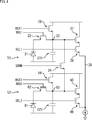
- FIG. 4 shows another configuration of the pixel of the solid-state imaging device that can change the conversion efficiency.
- portions corresponding to those in FIG. 1 are denoted by the same reference numerals, and description thereof is omitted as appropriate.
- one pixel 51 is provided with a photoelectric conversion unit 21, a charge transfer unit 22, an FD unit 23, a connection switch 24, a reset transistor 26, an amplification transistor 27, and a selection transistor 28.
- the pixel 52 adjacent to the pixel 51 is provided with a photoelectric conversion unit 61, a charge transfer unit 62, an FD unit 63, a connection switch 24, a reset transistor 64, an amplification transistor 65, and a selection transistor 66.
- the photoelectric conversion unit 61, the charge transfer unit 62, the FD unit 63, the reset transistor 64, the amplification transistor 65, and the selection transistor 66 are respectively the photoelectric conversion unit 21, the charge transfer unit 22, the FD unit 23, the reset transistor 26, Corresponding to the amplification transistor 27 and the selection transistor 28, the same operation is performed.
- the FD unit 63 has a parasitic capacitance C21.
- connection switch 24 is provided between the FD unit 23 and the FD unit 63, and electrically connects the FD unit 23 and the FD unit 63.
- the charges transferred from the photoelectric conversion unit 21 via the charge transfer unit 22 are accumulated in the electrically connected FD unit 23 and FD unit 63. Can do.
- the charges transferred from the photoelectric conversion unit 61 via the charge transfer unit 62 can be stored in the FD unit 23 and the FD unit 63 that are electrically connected.
- the drive signal TRG1, the drive signal RST1, and the drive signal SEL1 are supplied to the charge transfer unit 22, the reset transistor 26, and the selection transistor 28.
- the drive signal TRG2, the drive signal RST2, and the drive signal SEL2 are supplied to the charge transfer unit 62, the reset transistor 64, and the selection transistor 66.
- the charge is accumulated only in the FD unit 23 when a small signal with a small amount of received light is set to high conversion efficiency, and the charge is accumulated in the FD unit 23 and the FD unit 63 when a large signal with a large amount of received light.
- the conversion efficiency into the electric signal can be switched as appropriate.
- the conversion efficiency can be switched in the pixel 52.
- each drive signal shows a state in which the bump state is high level in the drawing, and a state in which the bump state is low level in the drawing.
- the pixel 51 exposure of the photoelectric conversion unit 21 is started at a predetermined timing. Then, from the state where each drive signal is at the low level, at time t21, the drive signal SEL1 and the drive signal SEL2 are set to the high level, the selection transistor 28 and the selection transistor 66 are turned on, and the pixel 51 and the pixel 52 are selected.
- the drive signal CONN is also set to the high level, the connection switch 24 is turned on, and the FD unit 23 and the FD unit 63 are electrically connected.
- the drive signal RST1 and the drive signal RST2 are set to the high level, the reset transistor 26 and the reset transistor 64 are turned on, and the potentials of the FD unit 23 and the FD unit 63 are reset. Thereafter, at time t23, the drive signal RST1 and the drive signal RST2 are set to the low level, the reset transistor 26 and the reset transistor 64 are turned off, and the reset is released.
- an electric signal corresponding to the electric charge accumulated in the FD unit 23 and the FD unit 63 between time t24 and time t25 is output from the amplification transistor 27 to the vertical signal line 29 via the selection transistor 28 as a reset level.
- the drive signal TRG1 is set to the high level, the charge transfer unit 22 is turned on, and the charges obtained by the photoelectric conversion in the photoelectric conversion unit 21 are transferred to the FD unit 23 and the FD unit 63 via the charge transfer unit 22. Forwarded to Thereafter, when the drive signal TRG1 is set to the low level at time t27 and the charge transfer unit 22 is turned off, the transfer of charges from the photoelectric conversion unit 21 is completed, and the exposure in the photoelectric conversion unit 21 is completed.
- an electric signal corresponding to the electric charge accumulated in the FD unit 23 and the FD unit 63 between time t28 and time t29 is output from the amplification transistor 27 to the vertical signal line 29 via the selection transistor 28 as a signal level.
- the drive signal TRG1 is set to the high level and the signal corresponding to the electric charge obtained by the photoelectric conversion unit 21 is read by the source follower circuit including the amplification transistor 27 and the like has been described.
- the drive signal TRG2 can be set to the high level, and a signal corresponding to the electric charge obtained by the photoelectric conversion unit 61 can be read out by the source follower circuit including the amplification transistor 65 and the like.
- the drive signal TRG1 and the drive signal TRG2 are simultaneously set to the high level, and a signal corresponding to the electric charge obtained by both the photoelectric conversion unit 21 and the photoelectric conversion unit 61 is converted into a source follower circuit including the amplification transistor 27 and the amplification transistor. It is also possible to read from a source follower circuit consisting of 65 grades.
- the conversion efficiency can also be varied by electrically connecting the FD section between adjacent pixels by a connection switch.
- connection switch 24 when the conversion efficiency is low, the connection switch 24 is turned on when the signal level is read.
- the capacities of the FD unit 23 and the FD unit 63 greatly vary. If it does so, the linearity at the time of signal reading will also deteriorate, and the quality of the image obtained with a solid-state image sensor will fall.
- the pixel configuration is such that the FD portions of adjacent pixels connected to the same vertical signal line can be electrically connected by a connection switch. Further, when the signal level is read when the conversion efficiency is low, the connection switch is turned off to suppress the deterioration of the linearity due to the capacitance variation and obtain a higher quality image.
- a solid-state imaging device to which the present technology is applied has a configuration shown in FIG.
- the solid-state imaging device 91 illustrated in FIG. 6 is a solid-state imaging device such as a CMOS (Complementary Metal Metal Oxide Semiconductor) image sensor.
- CMOS Complementary Metal Metal Oxide Semiconductor
- the solid-state imaging device 91 has a configuration including a pixel array unit 101 formed on a semiconductor substrate (chip) (not shown) and a peripheral circuit unit integrated on the same semiconductor substrate as the pixel array unit 101.
- the peripheral circuit unit includes, for example, a vertical drive unit 102, a column processing unit 103, a horizontal drive unit 104, and a system control unit 105.
- the solid-state imaging device 91 further includes a signal processing unit 108 and a data storage unit 109.
- the signal processing unit 108 and the data storage unit 109 may be mounted on the same substrate as the solid-state image sensor 91 or may be arranged on a different substrate from the solid-state image sensor 91.
- Each processing of the signal processing unit 108 and the data storage unit 109 may be processing by an external signal processing unit provided on a substrate different from the solid-state imaging device 91, for example, a DSP (Digital Signal Processor) circuit or software. .
- a DSP Digital Signal Processor
- the pixel array unit 101 generates unit charges (hereinafter also simply referred to as pixels) having a photoelectric conversion unit that generates and accumulates charges according to the amount of received light.
- the configuration is two-dimensionally arranged.
- the row direction refers to the arrangement direction of the pixels in the pixel row (that is, the horizontal direction)
- the column direction refers to the arrangement direction of the pixels in the pixel column (that is, the vertical direction). That is, the row direction is the horizontal direction in the figure, and the column direction is the vertical direction in the figure.
- the pixel drive lines 106 are wired in the row direction for each pixel row and the vertical signal lines 107 are wired in the column direction for each pixel column in the matrix pixel arrangement. .
- the pixel drive line 106 transmits a drive signal for performing driving when reading a signal from the pixel.
- the pixel drive line 106 is shown as one wiring, but is not limited to one.
- One end of the pixel drive line 106 is connected to an output end corresponding to each row of the vertical drive unit 102.
- the vertical drive unit 102 is configured by a shift register, an address decoder, and the like, and drives each pixel of the pixel array unit 101 at the same time or in units of rows. That is, the vertical drive unit 102 constitutes a drive unit that controls the operation of each pixel of the pixel array unit 101 together with the system control unit 105 that controls the vertical drive unit 102.
- the vertical drive unit 102 is not shown in the figure for its specific configuration, but generally has a configuration having two scanning systems, a reading scanning system and a sweeping scanning system.
- a signal output from each unit pixel of the pixel row selectively scanned by the vertical driving unit 102 is input to the column processing unit 103 through the vertical signal line 107 for each pixel column.
- the column processing unit 103 performs predetermined signal processing on signals output from the pixels of the selected row through the vertical signal line 107 for each pixel column of the pixel array unit 101, and temporarily outputs the pixel signals after the signal processing. Hold on.
- the column processing unit 103 performs noise removal processing, sampling processing such as DDS (Double Data Sampling) and CDS (Correlated Double Sampling), AD conversion processing, and the like as signal processing.
- sampling processing such as DDS (Double Data Sampling) and CDS (Correlated Double Sampling)
- AD conversion processing and the like as signal processing.
- the horizontal driving unit 104 includes a shift register, an address decoder, and the like, and sequentially selects unit circuits corresponding to the pixel columns of the column processing unit 103. By the selective scanning by the horizontal driving unit 104, pixel signals that are signal-processed for each unit circuit in the column processing unit 103 are sequentially output.
- the system control unit 105 includes a timing generator that generates various timing signals, and the vertical driving unit 102, the column processing unit 103, the horizontal driving unit 104, and the like based on various timings generated by the timing generator. The drive control is performed.
- the signal processing unit 108 has at least an arithmetic processing function, and performs various signal processing such as arithmetic processing on the pixel signal output from the column processing unit 103.
- the data storage unit 109 temporarily stores data necessary for the signal processing in the signal processing unit 108.
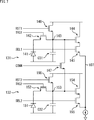
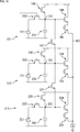
- FIG. 7 shows the configuration of the pixel 131 and the pixel 132 as two unit pixels connected to the same vertical signal line 107 arranged adjacent to each other in the column direction.
- the pixel 131 includes a photoelectric conversion unit 141, a charge transfer unit 142, an FD unit 143, an amplification transistor 144, a selection transistor 145, a reset transistor 146, and a connection switch 147.
- the pixel 132 includes a photoelectric conversion unit 151, a charge transfer unit 152, an FD unit 153, an amplification transistor 154, a selection transistor 155, a reset transistor 156, and a connection switch 147.
- the pixel 131 and the pixel 132 share one connection switch 147.
- the photoelectric conversion unit 141 includes, for example, a photodiode, photoelectrically converts light incident from the outside (subject), and accumulates the electric charge obtained as a result.
- the FD unit 143 is connected to the photoelectric conversion unit 141 via the charge transfer unit 142.
- the charge transfer unit 142 is formed of a transistor. When the drive signal TRG1 supplied to the gate of the charge transfer unit 142 becomes high level, the charge transfer unit 142 becomes conductive and transfers the charge accumulated in the photoelectric conversion unit 141 to the FD unit 143.
- the transistors such as the charge transfer unit 142, the selection transistor 145, the reset transistor 146, and the connection switch 147 are turned on, and the fact that these transistors are turned off. Also called off.
- the FD unit 143 has a parasitic capacitance C31, is a floating diffusion region called FD (Floating Diffusion), and temporarily accumulates the charge transferred from the photoelectric conversion unit 141 via the charge transfer unit 142.
- C31 parasitic capacitance
- FD floating Diffusion
- the amplifying transistor 144 has a drain connected to a power source and a gate connected to the FD unit 143, and reads a signal corresponding to the charge accumulated in the FD unit 143.
- the selection transistor 145 has a drain connected to the source of the amplification transistor 144 and a source connected to the vertical signal line 107. The selection transistor 145 is turned on when the drive signal SEL1 supplied to the gate becomes high level, and is read by the amplification transistor 144. The signal is output to the vertical signal line 107.
- a source follower circuit is configured by the amplification transistor 144, the selection transistor 145, and the constant current source connected to the vertical signal line 107. Therefore, the amplification transistor 144 functions as a reading unit that outputs a signal corresponding to the charge accumulated in the FD unit 143.
- the reset transistor 146 is connected between the power source and the FD unit 143.
- the reset transistor 146 is turned on when the drive signal RST1 supplied to the gate of the reset transistor 146 becomes a high level, and the FD unit 143 is set to a predetermined potential, that is, a power supply voltage. Reset to.
- the connection switch 147 includes a transistor and is provided between the FD unit 143 of the pixel 131 and the FD unit 153 of the pixel 132. That is, the drain of the connection switch 147 is connected to the FD unit 143, and the source of the connection switch 147 is connected to the FD unit 153.
- connection switch 147 becomes conductive when the drive signal CONN supplied to the gate of the connection switch 147 becomes high level, and electrically connects the FD unit 143 and the FD unit 153. Therefore, in this state, the conversion efficiency of electric charges into an electric signal is lower, that is, a low conversion efficiency state.
- connection switch 147 when the drive signal CONN is set to the low level, the connection switch 147 is turned off, and the FD portion 143 and the FD portion 153 are electrically disconnected (separated state), The signal conversion efficiency is higher than when the connection switch 147 is in a conductive state. That is, a high conversion efficiency state is obtained.
- the photoelectric conversion unit 151, the charge transfer unit 152, the FD unit 153, the amplification transistor 154, the selection transistor 155, and the reset transistor 156 of the pixel 132 are the same as the photoelectric conversion unit 141 to the reset transistor 146 of the pixel 131. The description is omitted.
- the FD unit 153 has a parasitic capacitance C32. Further, the drive signal TRG2, the drive signal SEL2, and the drive signal RST2 are supplied to the gates of the charge transfer unit 152, the selection transistor 155, and the reset transistor 156.
- the drive signal SEL1, the drive signal SEL2, the drive signal RST1, the drive signal RST2, the drive signal TRG1, the drive signal TRG2, and the drive signal CONN are transmitted from the vertical drive unit 102 via the pixel drive line 106. It is supplied to each transistor. That is, the vertical drive unit 102 controls the operation of each unit by supplying a drive signal to each unit pixel unit.
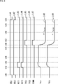
- the broken lines L41 to L47 indicate the drive signal SEL1, the drive signal SEL2, the drive signal RST1, the drive signal RST2, the drive signal TRG1, the drive signal TRG2, and the drive signal CONN, respectively.
- FIG. 8 shows a state in which each drive signal has a high level in the projecting state and a state in which the projecting state is at the low level.
- a curve L48 and a curve L49 indicate the potential of the FD unit 143 and the potential of the FD unit 153, respectively.
- the vertical drive unit 102 sets the drive signal SEL1 and the drive signal SEL2 to be supplied to the selection transistor 145 and the selection transistor 155 through the pixel drive line 106 to the high level. To do.
- the selection transistor 145 and the selection transistor 155 are turned on, and the pixel 131 and the pixel 132 are selected.
- the vertical drive unit 102 sets the drive signal RST1 and the drive signal RST2 supplied to the reset transistor 146 and the reset transistor 156 to a high level. Thereby, the reset transistor 146 and the reset transistor 156 are turned on, and the potentials of the FD unit 143 and the FD unit 153 are reset to the potential of the power source.
- the vertical drive unit 102 sets the drive signal RST1 and the drive signal RST2 supplied to the reset transistor 146 and the reset transistor 156 to a low level. Thereby, the reset transistor 146 and the reset transistor 156 are turned off, and the reset state of the FD unit 143 and the FD unit 153 is released. In this state, the potentials of the FD unit 143 and the FD unit 153 are the same as those of the power source.
- an electric signal corresponding to the electric charge accumulated in the FD unit 143 and the FD unit 153 between the time t44 and the time t45 is sent from the amplification transistor 144 and the amplification transistor 154 to the selection transistor 145 and the selection transistor 155 as a reset level. Via the vertical signal line 107.
- a voltage corresponding to the charge accumulated in the FD unit 143 is applied to the gate of the amplification transistor 144, and a current having a magnitude corresponding to the voltage is supplied from the amplification transistor 144 to the vertical signal line 107 via the selection transistor 145. And flow.
- a voltage corresponding to the charge accumulated in the FD unit 153 is applied to the gate of the amplification transistor 154, and a current having a magnitude corresponding to the voltage is applied from the amplification transistor 154 via the selection transistor 155 to the vertical signal line 107. It flows to. At this time, the FD unit 143 and the FD unit 153 are in an electrically separated state (separated state).
- the column processing unit 103 generates a signal indicating the reset level of the pixel 131 by detecting a voltage value corresponding to the sum of the current from the amplification transistor 144 and the current from the amplification transistor 154.
- the vertical drive unit 102 sets the drive signal CONN supplied to the gate of the connection switch 147 to the high level and sets the drive signal TRG1 supplied to the charge transfer unit 142 to the high level.
- connection switch 147 is turned on and the FD unit 143 and the FD unit 153 are electrically connected.
- the charge transfer unit 142 is turned on by the drive signal TRG1, and the charge obtained by the photoelectric conversion by the photoelectric conversion unit 141 is transferred from the photoelectric conversion unit 141 via the charge transfer unit 142.
- the potentials of the FD unit 143 and the FD unit 153 are lowered according to the transferred charges.
- the vertical drive unit 102 sets the drive signal CONN supplied to the gate of the connection switch 147 to the low level at time t47 and sets the drive signal TRG1 supplied to the charge transfer unit 142 to the low level.
- connection switch 147 is turned off and the charge transfer unit 142 is also turned off.
- the charge transfer unit 142 is turned off, the exposure of the pixel 131 is completed.
- the connection switch 147 is turned off, the electric charge obtained by the photoelectric conversion unit 141 receiving light from the outside and performing photoelectric conversion is divided and accumulated in the FD unit 143 and the FD unit 153. It will be.
- an electric signal corresponding to the electric charge that is divided and accumulated in the FD unit 143 and the FD unit 153 between time t48 and time t49 is transmitted as a signal level from the amplification transistor 144 and the amplification transistor 154 to the selection transistor 145 and The signal is output to the vertical signal line 107 via the selection transistor 155.
- a voltage corresponding to the charge accumulated in the FD unit 143 is applied to the gate of the amplification transistor 144, and a current having a magnitude corresponding to the voltage is supplied from the amplification transistor 144 to the vertical signal line 107 via the selection transistor 145. And flow.
- a voltage corresponding to the charge accumulated in the FD unit 153 is applied to the gate of the amplification transistor 154, and a current having a magnitude corresponding to the voltage is applied from the amplification transistor 154 via the selection transistor 155 to the vertical signal line 107. It flows to.
- the electric charge obtained by the photoelectric conversion unit 141 is divided and accumulated in the FD unit 143 and the FD unit 153. Yes.
- a current corresponding to the electric charge accumulated in the FD unit 143 and a current corresponding to the electric charge accumulated in the FD unit 153 flow through the vertical signal line 107, the photoelectric conversion unit 141 eventually obtained the current.
- a signal corresponding to the total charge is read out.
- the FD unit 143 and the FD unit 153 are electrically separated after the charge transfer, but the charge obtained by the photoelectric conversion is accumulated separately in the FD unit 143 and the FD unit 153.
- Such driving is read driving with low conversion efficiency.
- the column processing unit 103 generates a signal indicating the signal level of the pixel 131 by detecting a voltage value corresponding to the sum of the current from the amplification transistor 144 and the current from the amplification transistor 154. Then, the column processing unit 103 generates a pixel signal of the pixel 131 from the signal level and the reset level read in this way, and outputs the pixel signal to the signal processing unit 108.
- connection switch 147 when the signal level is read from the pixel 131, the signal is read with the connection switch 147 turned off. Therefore, since the voltage between the gate and the source of the connection switch 147 becomes a value within the range of the section A11 shown in FIG. 3, the parasitic of the connection switch 147 with respect to the amount of charge obtained by the photoelectric conversion unit 141 during the exposure period. Capacitance fluctuations can be kept small. Thereby, sufficient linearity can be realized at the time of signal reading. That is, linearity can be improved.
- connection switch 147 When the connection switch 147 is turned off, the connection switch 147 becomes a noise source, positive kT / C noise is generated in the FD unit 143 on the drain side of the connection switch 147, and the FD unit on the source side of the connection switch 147. In 153, negative kT / C noise is generated.
- the vertical driving unit 102 sets the driving signal SEL1 and the driving signal SEL2 supplied to the selection transistor 145 and the selection transistor 155 to a low level.
- the selection transistor 145 and the selection transistor 155 are turned off, and the pixel 131 and the pixel 132 are in a non-selected state.
- the solid-state imaging device 91 transfers the charge obtained by the photoelectric conversion unit 141 to the FD unit 143 and the FD unit 153, and then turns off the connection switch 147 to switch the FD unit 143 and the FD unit 153. Separate electrically.
- the solid-state image sensor 91 outputs a signal corresponding to the charges accumulated in the FD unit 143 and the FD unit 153 in a state where the FD unit 143 and the FD unit 153 are separated, that is, in a state where the connection switch 147 is turned off. Read as level.
- the solid-state image sensor 91 it can suppress that the parasitic capacitance of the connection switch 147 changes with the quantity of the electric charge obtained in the photoelectric conversion part 141. FIG. Thereby, the linearity at the time of signal reading can be improved, and a higher quality image can be obtained.
- the signal corresponding to the charge obtained by the photoelectric conversion unit 141 of the pixel 131 is read has been described as an example.
- the signal corresponding to the charge obtained by the photoelectric conversion unit 151 of the pixel 132 is read.
- the same operation may be performed.
- a signal corresponding to the electric charge obtained by both the photoelectric conversion unit 141 and the photoelectric conversion unit 151 may be read by performing the same operation.
- the reading of the signal corresponding to the electric charge accumulated in the FD unit 143 and the reading of the signal corresponding to the electric charge accumulated in the FD unit 153 do not necessarily have to be performed simultaneously.
- connection switch 147 remains off when the FD unit 143 and the FD unit 153 are reset has been described. However, the FD unit 143 and the FD unit 153 are reset with the connection switch 147 on. You may do it.
- the solid-state imaging device 91 performs the operation shown in FIG.
- the operation of the solid-state imaging device 91 will be described with reference to the timing chart of FIG. 9, taking as an example a case where a signal obtained by receiving light at the pixel 131 is read out in a low conversion efficiency state.
- FIG. 9 parts corresponding to those in FIG. 8 are denoted by the same reference numerals, and description thereof will be omitted as appropriate.
- the broken lines L51 to L53 indicate the drive signal RST1, the drive signal RST2, and the drive signal CONN, respectively.
- the vertical drive unit 102 sets the drive signal RST1 and the drive signal RST2 to high level at the time t42 and also sets the drive signal CONN to high level.
- connection switch 147 is turned on so that the FD unit 143 and the FD unit 153 are electrically connected. In such a state, the FD unit 143 and the FD unit 153 are reset.
- the vertical drive unit 102 sets the drive signal RST1 and the drive signal RST2 to a low level to turn off the reset transistor 146 and the reset transistor 156, thereby releasing the reset of the FD unit 143 and the FD unit 153.
- connection switch 147 When the connection switch 147 is turned on when the FD unit 143 and the FD unit 153 are reset, the connection switch 147 may be turned off before the reset is released.
- the solid-state image sensor 91 performs the operation shown in FIG.
- the operation of the solid-state imaging device 91 will be described with reference to the timing chart of FIG. 10, taking as an example a case where a signal obtained by receiving light at the pixel 131 is read out in a low conversion efficiency state.
- FIG. 10 parts corresponding to those in FIG. 8 are denoted by the same reference numerals, and description thereof will be omitted as appropriate.
- a broken line L61 indicates the drive signal CONN.
- the vertical drive unit 102 sets the drive signal RST1 and the drive signal RST2 to high level at the time t42 and also sets the drive signal CONN to high level.
- the FD unit 143 and the FD unit 153 are reset in a state where the FD unit 143 and the FD unit 153 are electrically connected.
- the solid-state imaging device 91 performs the operation shown in FIG.
- the operation of the solid-state imaging device 91 will be described with reference to the timing chart of FIG. 11, taking as an example a case where a signal obtained by receiving light at the pixel 131 is read in a low conversion efficiency state.
- FIG. 11 parts corresponding to those in FIG. 10 are denoted by the same reference numerals, and description thereof will be omitted as appropriate.
- a broken line L71 indicates the drive signal RST2.
- the vertical drive unit 102 sets the drive signal RST1 to the high level at time t42 and also sets the drive signal CONN to the high level. At this time, the drive signal RST2 is kept at a low level.
- the reset transistor 146 is turned on while the FD unit 143 and the FD unit 153 are electrically connected, and the FD unit 143 and the FD unit 153 are reset. At this time, the reset transistor 156 remains off.
- the vertical drive unit 102 electrically separates the FD unit 143 and the FD unit 153 by turning off the connection switch 147 by setting the drive signal CONN to a low level. Furthermore, when the vertical drive unit 102 sets the drive signal RST1 to the low level to turn off the reset transistor 146 at time t43, the same drive as in FIG. 10 is performed thereafter.
- the solid-state imaging device 91 performs the operation shown in FIG.
- the operation of the solid-state imaging device 91 will be described with reference to the timing chart of FIG. 12, taking as an example a case where a signal obtained by receiving light at the pixel 131 is read out in a low conversion efficiency state.
- FIG. 12 parts corresponding to those in FIG. 10 are denoted by the same reference numerals, and description thereof will be omitted as appropriate.
- the broken line L81 indicates the drive signal RST1.
- the vertical drive unit 102 sets the drive signal RST2 to the high level and also sets the drive signal CONN to the high level at time t42. At this time, the drive signal RST1 is kept at a low level.
- the reset transistor 156 is turned on while the FD unit 143 and the FD unit 153 are electrically connected, and the FD unit 143 and the FD unit 153 are reset. At this time, the reset transistor 146 remains off.
- the vertical drive unit 102 electrically separates the FD unit 143 and the FD unit 153 by turning off the connection switch 147 by setting the drive signal CONN to a low level. Furthermore, when the vertical drive unit 102 sets the drive signal RST2 to the low level to turn off the reset transistor 156 at time t43, the same drive as in FIG. 10 is performed thereafter.
- the solid-state imaging device 91 performs the operation shown in FIG.
- the operation of the solid-state imaging device 91 will be described with reference to the timing chart of FIG. 13, taking as an example the case where a signal obtained by receiving light at the pixel 131 is read in a low conversion efficiency state.
- FIG. 13 parts corresponding to those in FIG. 9 are denoted by the same reference numerals, and description thereof will be omitted as appropriate.
- a broken line L91 indicates the drive signal RST2.
- the vertical drive unit 102 sets the drive signal RST1 to the high level at time t42 and also sets the drive signal CONN to the high level. At this time, the drive signal RST2 is kept at a low level.
- the reset transistor 146 is turned on while the FD unit 143 and the FD unit 153 are electrically connected, and the FD unit 143 and the FD unit 153 are reset. At this time, the reset transistor 156 remains off.
- the vertical drive unit 102 turns off the reset transistor 146 by setting the drive signal RST1 to the low level, and releases the reset of the FD unit 143 and the FD unit 153.
- the solid-state imaging device 91 performs the operation shown in FIG.
- the operation of the solid-state imaging device 91 will be described with reference to the timing chart of FIG. 14, taking as an example a case where a signal obtained by receiving light at the pixel 131 is read out in a low conversion efficiency state.
- FIG. 14 the same reference numerals are given to the portions corresponding to those in FIG. 9, and the description thereof will be omitted as appropriate.
- the broken line L101 indicates the drive signal RST1.
- the vertical drive unit 102 sets the drive signal RST2 to the high level and also sets the drive signal CONN to the high level at time t42. At this time, the drive signal RST1 is kept at a low level.
- the reset transistor 156 is turned on while the FD unit 143 and the FD unit 153 are electrically connected, and the FD unit 143 and the FD unit 153 are reset. At this time, the reset transistor 146 remains off.
- the vertical drive unit 102 turns off the reset transistor 156 by setting the drive signal RST2 to a low level, and releases the reset of the FD unit 143 and the FD unit 153.
- the pixel 131 is further provided with a photoelectric conversion unit 181 and a charge transfer unit 182 in addition to the configuration of the pixel 131 illustrated in FIG. 7.
- the photoelectric conversion unit 181 is connected to the FD unit 143 via the charge transfer unit 182. Therefore, by turning on the charge transfer unit 182, charges obtained by photoelectric conversion in the photoelectric conversion unit 181 can be transferred to the FD unit 143 via the charge transfer unit 182 and accumulated.
- only the charge obtained by the photoelectric conversion unit 141 may be transferred to the FD unit 143, or only the charge obtained by the photoelectric conversion unit 181 is transferred to the FD unit. 143 may be transferred.
- both the charge obtained by the photoelectric conversion unit 141 and the charge obtained by the photoelectric conversion unit 181 are transferred to the FD unit 143. You may make it do. In this case, the charges obtained by the photoelectric conversion unit 141 and the photoelectric conversion unit 181 are added by the FD unit 143.
- the pixel 132 is also provided with two photoelectric conversion units in the same manner as the pixel 131. That is, the pixel 132 is further provided with a photoelectric conversion unit 183 and a charge transfer unit 184 in addition to the configuration of the pixel 132 illustrated in FIG.
- the photoelectric conversion unit 183 is connected to the FD unit 153 via the charge transfer unit 184. Therefore, by turning on the charge transfer unit 184, the charge obtained by the photoelectric conversion in the photoelectric conversion unit 183 can be transferred to the FD unit 153 via the charge transfer unit 184 and stored.
- either one or both of the charge obtained by the photoelectric conversion unit 183 and the charge obtained by the photoelectric conversion unit 151 can be transferred to the FD unit 153 and accumulated.
- the connection switch 147 can be turned on to electrically connect the FD unit 143 and the FD unit 153, as shown in FIGS. The same driving as that described with reference to FIG.
- the unit pixels provided in the solid-state imaging device 91 are configured as shown in FIG. In FIG. 16, the same reference numerals are given to the portions corresponding to those in FIG. 7, and the description thereof will be omitted as appropriate.
- FIG. 16 shows the configuration of three pixels 131, a pixel 132, and a pixel 211. These pixel 131, pixel 132, and pixel 211 are connected to the same vertical signal line 107.
- the pixel 211 includes a photoelectric conversion unit 221, a charge transfer unit 222, an FD unit 223, an amplification transistor 224, a selection transistor 225, a reset transistor 226, and a connection switch 227.
- the FD unit 223 has a parasitic capacitance C41.
- each of the photoelectric conversion units 221 to the connection switch 227 constituting the pixel 211 is the same as each of the photoelectric conversion units 141 to the connection switch 147 of the pixel 131, and thus description thereof will be omitted as appropriate.
- the configuration of the pixel 131 is the same as the configuration of the pixel 131 shown in FIG. Further, the configuration of the pixel 132 is a configuration in which a connection switch 227 is further provided in the FD unit 153 with respect to the configuration of the pixel 132 illustrated in FIG. 7.
- connection switch 227 is shared by the pixel 132 and the pixel 211.
- the FD unit 153 of the pixel 132 and the FD unit 223 of the pixel 211 are connected via the connection switch 227.
- the connection switch 147 is turned on as described above, the FD unit 143 and the FD unit 153 are electrically connected, and the photoelectric conversion unit is connected to the FD unit 143 and the FD unit 153.
- the charge obtained in 141 can be accumulated.
- the total capacity of the FD unit is twice that in the case where charges are accumulated only in the FD unit 143.
- connection switch 147 and the connection switch 227 are simultaneously turned on at the time of reading a signal from the pixel 131, the FD unit 143, the FD unit 153, and the FD unit 223 are electrically connected, and the FD unit 143 and the FD unit are connected. 153 and the FD unit 223 can store the charge obtained by the photoelectric conversion unit 141.
- the total capacity of the FD unit is three times that in the case where charges are accumulated only in the FD unit 143.
- what is necessary is just to select suitably how many times the total capacity
- ⁇ Fourth embodiment> ⁇ Pixel configuration example> Further, the example in which the unit pixels arranged in the column direction such as the pixel 131 and the pixel 132 are connected to the same vertical signal line 107 has been described above. However, the FD units are electrically connected to each other via the connection switch. Some or all of two or more possible unit pixels may be connected to different vertical signal lines 107.
- the unit pixels provided in the solid-state imaging device 91 are configured as shown in FIG. In FIG. 17, the same reference numerals are given to portions corresponding to those in FIG. 7, and description thereof will be omitted as appropriate.
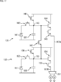
- FIG. 17 shows the configuration of the pixel 131 and the pixel 132 as unit pixels, and the configuration of the pixel 131 and the pixel 132 is the same as the configuration of the pixel 131 and the pixel 132 shown in FIG. ing. However, in the example shown in FIG. 17, the selection transistor 145 of the pixel 131 and the selection transistor 155 of the pixel 132 are connected to different vertical signal lines 107.
- the selection transistor 145 is connected to the vertical signal line 107A as the vertical signal line 107
- the selection transistor 155 is connected to the vertical signal line 107B as the vertical signal line 107.
- the two vertical signal lines 107A and 107B are connected to an adder 251 provided in the column processing unit 103.
- the adder 251 receives the signal supplied from the selection transistor 145 via the vertical signal line 107A and the selection transistor 155 via the vertical signal line 107B. The supplied signals are added, and the addition result is finally output as a signal read from the pixel 131.
- the adder 251 may add the signal output from the selection transistor 145 and the signal output from the selection transistor 155 before AD conversion is performed on these signals, or after AD conversion. May be.
- the present technology provides an electronic device that uses a solid-state imaging device for a photoelectric conversion unit, such as an imaging device such as a digital still camera or a video camera, a portable terminal device having an imaging function, or a copying machine that uses a solid-state imaging device for an image reading unit. Applicable to all devices.
- FIG. 18 is a diagram illustrating a configuration example of an imaging apparatus as an electronic apparatus to which the present technology is applied.
- the 18 includes an optical unit 911 including a lens group, a solid-state imaging device (imaging device) 912, and a DSP circuit 913 that is a camera signal processing circuit.
- the imaging device 901 also includes a frame memory 914, a display unit 915, a recording unit 916, an operation unit 917, and a power supply unit 918.
- the DSP circuit 913, the frame memory 914, the display unit 915, the recording unit 916, the operation unit 917, and the power supply unit 918 are connected to each other via a bus line 919.
- the optical unit 911 takes in incident light (image light) from a subject and forms an image on the imaging surface of the solid-state imaging device 912.
- the solid-state imaging device 912 converts the amount of incident light imaged on the imaging surface by the optical unit 911 into an electrical signal in units of pixels and outputs the electrical signal.
- the solid-state image sensor 912 corresponds to the solid-state image sensor 91 shown in FIG.
- the display unit 915 includes, for example, a panel display device such as a liquid crystal panel or an organic EL (electroluminescence) panel, and displays a moving image or a still image captured by the solid-state imaging device 912.
- the recording unit 916 records a moving image or a still image captured by the solid-state imaging device 912 on a recording medium such as a video tape or a DVD (Digital Versatile Disk).
- the operation unit 917 issues operation commands for various functions of the imaging device 901 under the operation of the user.
- the power supply unit 918 appropriately supplies various power sources serving as operation power sources for the DSP circuit 913, the frame memory 914, the display unit 915, the recording unit 916, and the operation unit 917 to these supply targets.
- the present invention is applied to a CMOS image sensor in which pixels that detect signal charges corresponding to the amount of visible light as physical quantities are arranged in a matrix has been described as an example.
- the present technology is not limited to application to a CMOS image sensor, and can be applied to all solid-state imaging devices.
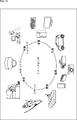
- FIG. 19 is a diagram illustrating a usage example in which the above-described solid-state imaging device (image sensor) is used.
- the solid-state imaging device described above can be used in various cases for sensing light such as visible light, infrared light, ultraviolet light, and X-ray as follows.
- Devices for taking images for viewing such as digital cameras and mobile devices with camera functions
- Devices used for traffic such as in-vehicle sensors that capture the back, surroundings, and interiors of vehicles, surveillance cameras that monitor traveling vehicles and roads, and ranging sensors that measure distances between vehicles, etc.
- Equipment used for home appliances such as TVs, refrigerators, air conditioners, etc. to take pictures and operate the equipment according to the gestures ⁇ Endoscopes, equipment that performs blood vessel photography by receiving infrared light, etc.
- Equipment used for medical and health care ⁇ Security equipment such as security surveillance cameras and personal authentication cameras ⁇ Skin measuring instrument for photographing skin and scalp photography Such as a microscope to do beauty Equipment used for sports-Equipment used for sports such as action cameras and wearable cameras for sports applications-Used for agriculture such as cameras for monitoring the condition of fields and crops apparatus
- the present technology can be configured as follows.
- a photoelectric conversion unit that photoelectrically converts incident light; and A first diffusion region for accumulating charges obtained by the photoelectric conversion;
- a first readout unit that outputs a signal corresponding to the charge accumulated in the first diffusion region;
- a second diffusion region connected to the first diffusion region and storing charge;
- a first connection switch provided between the first diffusion region and the second diffusion region and electrically connecting the first diffusion region and the second diffusion region;
- a second readout unit that outputs a signal corresponding to the charge accumulated in the second diffusion region;
- the solid-state imaging device further including an adding unit that adds the signal output from the first reading unit and the signal output from the second reading unit.
- the photoelectric conversion unit, the first diffusion region, and the first readout unit are provided in predetermined pixels, and the second diffusion region and the second readout unit are connected to the predetermined pixels. Are provided in different pixels.
- the solid-state imaging device according to any one of (1) to (4).
- (6) The solid-state imaging device according to any one of (1) to (5), wherein the plurality of photoelectric conversion units are connected to the first diffusion region.
- a third diffusion region connected to the second diffusion region and storing charge;
- a second connection switch provided between the second diffusion region and the third diffusion region and electrically connecting the second diffusion region and the third diffusion region;
- the solid-state imaging device according to any one of 1) to (6).
- a photoelectric conversion unit that photoelectrically converts incident light; and A first diffusion region for accumulating charges obtained by the photoelectric conversion;
- a first readout unit that outputs a signal corresponding to the charge accumulated in the first diffusion region;
- a second diffusion region connected to the first diffusion region and storing charge;
- a connection switch provided between the first diffusion region and the second diffusion region and electrically connecting the first diffusion region and the second diffusion region;
- a solid-state imaging device driving method comprising: a second readout unit that outputs a signal corresponding to the charge accumulated in the second diffusion region, The connection switch is controlled to electrically connect the first diffusion region and the second diffusion region, and the charge obtained by the photoelectric conversion is transferred to the first diffusion region and the second diffusion region.
- connection switch is controlled to electrically separate the first diffusion region and the second diffusion region, and a signal corresponding to the charge accumulated in the first diffusion region is read out from the first readout region. And outputting a signal corresponding to the charge accumulated in the second diffusion region from the second readout unit.
- 91 solid-state imaging device 101 pixel array unit, 102 vertical drive unit, 103 column processing unit, 131 pixel, 132 pixel, 141 photoelectric conversion unit, 142 charge transfer unit, 143 FD unit, 144 amplification transistor, 147 connection switch, 151 photoelectric Conversion unit, 152 charge transfer unit, 153 FD unit, 154 amplification transistor
Landscapes
- Engineering & Computer Science (AREA)
- Multimedia (AREA)
- Signal Processing (AREA)
- Solid State Image Pick-Up Elements (AREA)
Abstract
本技術は、より高品質な画像を得ることができるようにする固体撮像素子および駆動方法、並びに電子機器に関する。 光電変換部は、入射した光を光電変換し、電荷転送部は光電変換により得られた電荷を、光電変換部からFD部に転送する。このとき、接続スイッチはFD部と他のFD部とを電気的に接続し、FD部に転送されてきた電荷をFD部と他のFD部に蓄積させた後、FD部と他のFD部とを電気的に分離させる。増幅トランジスタは、FD部に蓄積されている電荷に応じた信号を垂直信号線に出力し、他の増幅トランジスタも、他のFD部に蓄積されている電荷に応じた信号を垂直信号線に出力する。本技術は固体撮像素子に適用することができる。
Description
本技術は固体撮像素子および駆動方法、並びに電子機器に関し、特に、より高品質な画像を得ることができるようにした固体撮像素子および駆動方法、並びに電子機器に関する。
従来、画像を撮影する固体撮像素子において、各画素で受光により得られた電荷の電気信号への変換効率を変更できるようにするものがある。
そのような固体撮像素子では、各画素は、受光した光を光電変換し、得られた電荷を蓄積する光電変換部と、光電変換部に蓄積された電荷を転送する電荷転送部と、電荷転送部を介して光電変換部から転送されてきた電荷を蓄積するFD(Floating Diffusion)部とを有している。そして、FD部に蓄積された電荷に対応する信号が、増幅トランジスタ等を介して垂直信号線に出力される。
また、FD部には接続スイッチを介して付加容量が接続されており、必要に応じてFD部と付加容量とが接続スイッチにより電気的に接続される。
光電変換部で得られた電荷をFD部と、そのFD部に電気的に接続された付加容量とに蓄積し、その電荷を信号として読み出せば変換効率が低くなる。逆に、光電変換部で得られた電荷をFD部のみに蓄積し、その電荷を信号として読み出すと変換効率は高くなる。
例えば、高照度時など光電変換部に入射する光の光量が多いとき、つまり電荷量が多い大信号を光電変換部からFD部に転送するときには、大きなダイナミックレンジが必要となる。このことから、最大信号量は垂直信号線後段のAD(Analog Digital)変換器で検出可能な電圧値の範囲やFD部の容量の制約を受けることになる。
そのため、大信号転送時にはFD部と付加容量を電気的に接続し、接続されたFD部と付加容量に電荷を蓄積するようにして変換効率を下げる必要がある。
しかし、入射する光の光量が少ない小信号転送時においてもFD部と付加容量を電気的に接続した状態で、それらのFD部と付加容量に電荷を蓄積し、信号の読み出しを行うとSNR(Signal to Noise Ratio)が悪化してしまう。
そこで、固体撮像素子では、大信号時にはFD部と付加容量を電気的に接続して変換効率を下げ、小信号時にはFD部と付加容量を電気的に切り離して変換効率を上げることで、信号量の制約とノイズの悪化の両方に対応するようにしている。
また、各画素で変換効率を変更できるようにした固体撮像素子として、受光面において上下に隣接する画素間で、互いのFD部を利用することができるようにしたものも提案されている(例えば、特許文献1参照)。
この固体撮像素子では、画素内のFD部と、その画素に隣接する画素内のFD部との間に接続スイッチが設けられている。
したがって、接続スイッチをオンして2つのFD部を接続した状態で、一方の画素の光電変換部で得られた電荷をそれらの接続されたFD部に蓄積して信号の読み出しを行えば、変換効率を低くすることができる。逆に、接続スイッチをオフして、画素内の光電変換部で得られた電荷を、その画素内のFD部のみに蓄積し、信号の読み出しを行うと変換効率を高くすることができる。
ところで、上述したFD部と付加容量を接続する接続スイッチや、隣接する画素間のFD部を接続する接続スイッチには寄生容量がある。
接続スイッチがオフの状態、つまり非導通状態であるときには、この寄生容量の変動は少ないため、信号の読み出しに特に影響は生じない。
しかし、接続スイッチがオンの状態、つまり導通状態であるときには、接続スイッチのゲートとソース間の電圧によって寄生容量が大きく変動してしまう。接続スイッチにはFD部が接続されていることから、FD部の容量には寄生容量が付加されることになる。
そうすると、光電変換部で得られた電荷の量によって寄生容量が付加されたFD部の総容量が変動することになり、光電変換部で得られた電荷の量と、その電荷に応じて画素から読み出される信号とのリニアリティ(線形性)が悪化してしまう。すなわち、光電変換部で得られた電荷の変化量に対して、画素から読み出される信号が非線形に変化してしまう。
このように信号読み出し時のリニアリティが悪化すると、固体撮像素子で高品質な画像を得ることができなくなってしまう。
本技術は、このような状況に鑑みてなされたものであり、より高品質な画像を得ることができるようにするものである。
本技術の第1の側面の固体撮像素子は、入射した光を光電変換する光電変換部と、前記光電変換により得られた電荷を蓄積する第1の拡散領域と、前記第1の拡散領域に蓄積された電荷に応じた信号を出力する第1の読み出し部と、前記第1の拡散領域に接続され、電荷を蓄積する第2の拡散領域と、前記第1の拡散領域と前記第2の拡散領域との間に設けられ、前記第1の拡散領域と前記第2の拡散領域とを電気的に接続する第1の接続スイッチと、前記第2の拡散領域に蓄積された電荷に応じた信号を出力する第2の読み出し部と、前記第1の接続スイッチを制御して前記第1の拡散領域と前記第2の拡散領域とを電気的に接続させて、前記光電変換により得られた電荷を前記第1の拡散領域および前記第2の拡散領域に蓄積させた後、前記第1の接続スイッチを制御して前記第1の拡散領域と前記第2の拡散領域とを電気的に分離させて、前記第1の拡散領域に蓄積された電荷に応じた信号を前記第1の読み出し部から出力させるとともに、前記第2の拡散領域に蓄積された電荷に応じた信号を前記第2の読み出し部から出力させる制御部とを備える。
前記第1の読み出し部および前記第2の読み出し部には、同じ垂直信号線に、電荷に応じた信号を出力させることができる。
前記第1の読み出し部および前記第2の読み出し部には、互いに異なる垂直信号線に、電荷に応じた信号を出力させることができる。
固体撮像素子には、前記第1の読み出し部から出力された信号と、前記第2の読み出し部から出力された信号とを加算する加算部をさらに設けることができる。
前記光電変換部、前記第1の拡散領域、および前記第1の読み出し部を所定の画素に設け、前記第2の拡散領域、および前記第2の読み出し部を、前記所定の画素とは異なる画素に設けることができる。
前記第1の拡散領域には、複数の前記光電変換部を接続することができる。
固体撮像素子には、前記第2の拡散領域に接続され、電荷を蓄積する第3の拡散領域と、前記第2の拡散領域と前記第3の拡散領域との間に設けられ、前記第2の拡散領域と前記第3の拡散領域とを電気的に接続する第2の接続スイッチとをさらに設けることができる。
本技術の第1の側面の駆動方法は、入射した光を光電変換する光電変換部と、前記光電変換により得られた電荷を蓄積する第1の拡散領域と、前記第1の拡散領域に蓄積された電荷に応じた信号を出力する第1の読み出し部と、前記第1の拡散領域に接続され、電荷を蓄積する第2の拡散領域と、前記第1の拡散領域と前記第2の拡散領域との間に設けられ、前記第1の拡散領域と前記第2の拡散領域とを電気的に接続する接続スイッチと、前記第2の拡散領域に蓄積された電荷に応じた信号を出力する第2の読み出し部とを備える固体撮像素子の駆動方法であって、前記接続スイッチを制御して前記第1の拡散領域と前記第2の拡散領域とを電気的に接続させて、前記光電変換により得られた電荷を前記第1の拡散領域および前記第2の拡散領域に蓄積させ、前記接続スイッチを制御して前記第1の拡散領域と前記第2の拡散領域とを電気的に分離させて、前記第1の拡散領域に蓄積された電荷に応じた信号を前記第1の読み出し部から出力させるとともに、前記第2の拡散領域に蓄積された電荷に応じた信号を前記第2の読み出し部から出力させるステップを含む。
本技術の第1の側面においては、入射した光を光電変換する光電変換部と、前記光電変換により得られた電荷を蓄積する第1の拡散領域と、前記第1の拡散領域に蓄積された電荷に応じた信号を出力する第1の読み出し部と、前記第1の拡散領域に接続され、電荷を蓄積する第2の拡散領域と、前記第1の拡散領域と前記第2の拡散領域との間に設けられ、前記第1の拡散領域と前記第2の拡散領域とを電気的に接続する接続スイッチと、前記第2の拡散領域に蓄積された電荷に応じた信号を出力する第2の読み出し部とを備える固体撮像素子において、前記接続スイッチが制御されて前記第1の拡散領域と前記第2の拡散領域とが電気的に接続されて、前記光電変換により得られた電荷を前記第1の拡散領域および前記第2の拡散領域に蓄積され、前記接続スイッチが制御されて前記第1の拡散領域と前記第2の拡散領域とが電気的に分離されて、前記第1の拡散領域に蓄積された電荷に応じた信号が前記第1の読み出し部から出力されるとともに、前記第2の拡散領域に蓄積された電荷に応じた信号が前記第2の読み出し部から出力される。
本技術の第2の側面の電子機器は、本技術の第1の側面の固体撮像素子と同様の構成とされる。
本技術の第1の側面および第2の側面によれば、より高品質な画像を得ることができる。
以下、図面を参照して、本技術を適用した実施の形態について説明する。
〈第1の実施の形態〉
〈リニアリティの悪化について〉
本技術は、FD部の容量値変動を小さく抑えることで、信号読み出し時のリニアリティを向上させ、より高品質な画像を得ることができるようにした固体撮像素子に関するものである。
〈リニアリティの悪化について〉
本技術は、FD部の容量値変動を小さく抑えることで、信号読み出し時のリニアリティを向上させ、より高品質な画像を得ることができるようにした固体撮像素子に関するものである。
まず、各画素で変換効率を変更できる固体撮像素子について説明する。
変換効率を変更できる固体撮像素子の画素の一般的な構成は、図1に示す構成とされる。
図1に示す画素11には、光電変換部21、電荷転送部22、FD部23、接続スイッチ24、付加容量25、リセットトランジスタ26、増幅トランジスタ27、および選択トランジスタ28が設けられている。
画素11では、光電変換部21が入射した光を受光して光電変換し、その結果得られた電荷を蓄積する。また、光電変換部21に蓄積された電荷は、電荷転送部22のゲートに供給される駆動信号TRGがハイレベルとなって電荷転送部22がオンされると、電荷転送部22を介してFD部23に転送される。
FD部23は寄生容量C11を有する浮遊拡散領域であり、光電変換部21から転送されてきた電荷を蓄積する。FD部23には、接続スイッチ24を介して付加容量25が接続されており、接続スイッチ24のゲートに供給される駆動信号CONNがハイレベルとなって接続スイッチ24がオンとされると、FD部23と付加容量25が電気的に接続される。この例では、接続スイッチ24のソースがFD部23に接続されている。
また、FD部23には、増幅トランジスタ27および選択トランジスタ28を介して垂直信号線29が接続されている。
選択トランジスタ28のゲートに供給される駆動信号SELがハイレベルとなって選択トランジスタ28がオンし、画素11が選択状態とされると、FD部23に蓄積されている電荷に応じた信号が、増幅トランジスタ27から選択トランジスタ28を介して垂直信号線29へと出力される。
さらにFD部23にはリセットトランジスタ26が接続されており、リセットトランジスタ26のゲートに供給される駆動信号RSTがハイレベルとされてリセットトランジスタ26がオンされると、FD部23が所定電位にリセットされる。
このような画素11では、FD部23と付加容量25が電気的に接続された状態で、それらのFD部23と付加容量25に光電変換部21からの電荷を蓄積し、その電荷に応じた信号を読み出すと、電荷の電気信号への変換効率はより低くなる。
逆にFD部23が付加容量25と電気的に切り離された状態で、FD部23に光電変換部21からの電荷を蓄積し、その電荷に応じた信号を読み出すと、電荷の電気信号への変換効率はより高くなる。すなわち、FD部23のみに電荷を蓄積する方が、FD部23と付加容量25に電荷を蓄積するよりも電気信号への変換効率はより高くなる。
そのため、画素11では、受光量が少ない小信号時にはFD部23のみに電荷が蓄積されるようにして高変換効率とされ、受光量が多い大信号時にはFD部23と付加容量25に電荷が蓄積されるようにして低変換効率とされる。このようにして画素11では電気信号への変換効率を適宜、切り替えることが可能である。
次に、図2のタイミングチャートを参照して、低変換効率時における画素11の動作について説明する。なお、図2において折れ線L11乃至折れ線L14は、それぞれ駆動信号SEL、駆動信号RST、駆動信号TRG、および駆動信号CONNを示している。また、図2では、各駆動信号が図中、上に突の状態がハイレベルである状態を示しており、下に突の状態がローレベルである状態を示している。
画素11では、所定のタイミングで光電変換部21の露光が開始される。そして、駆動信号SEL、駆動信号RST、駆動信号TRG、および駆動信号CONNがローレベルである状態から、時刻t1において駆動信号SELがハイレベルとされて選択トランジスタ28がオンされ、画素11が選択状態とされる。このとき駆動信号CONNもハイレベルとされて接続スイッチ24がオンされ、FD部23と付加容量25が電気的に接続される。
続く時刻t2では、駆動信号RSTがハイレベルとされてリセットトランジスタ26がオンされ、FD部23と付加容量25の電位がリセットされた後、時刻t3で駆動信号RSTがローレベルとされてリセットトランジスタ26がオフされ、リセットが解除される。
また、時刻t4から時刻t5の間でFD部23と付加容量25に蓄積されている電荷に応じた電気信号が、リセットレベルとして増幅トランジスタ27から選択トランジスタ28を介して垂直信号線29に出力される。
そして、時刻t6において駆動信号TRGがハイレベルとされて電荷転送部22がオンされ、光電変換部21で光電変換(露光)により得られた電荷が、電荷転送部22を介してFD部23および付加容量25へと転送される。その後、時刻t7において駆動信号TRGがローレベルとされて電荷転送部22がオフされると光電変換部21からの電荷の転送が終了され、光電変換部21での露光が終了する。
さらに、時刻t8から時刻t9の間でFD部23と付加容量25に蓄積されている電荷に応じた電気信号が、信号レベルとして増幅トランジスタ27から選択トランジスタ28を介して垂直信号線29に出力される。
ところで、上述したように接続スイッチ24のゲートとソース間の電圧に応じて、接続スイッチ24の寄生容量は変動する。
具体的には、例えば接続スイッチ24の寄生容量は、接続スイッチ24のゲートとソース間の電圧に応じて図3に示すように変動する。なお、図3において縦軸は接続スイッチ24の寄生容量を示しており、横軸は接続スイッチ24のゲートとソース間の電圧(以下、ゲート/ソース間電圧とも称する)を示している。
図3では、曲線L21は接続スイッチ24のゲートから見た接続スイッチ24の寄生容量を示しており、曲線L22は接続スイッチ24のゲートとソース間の寄生容量を示している。
例えば接続スイッチ24がオフの状態では、接続スイッチ24のゲート/ソース間電圧は、区間A11内の範囲の値となる。この区間A11内では、ゲートから見た接続スイッチ24の寄生容量は、ゲート/ソース間電圧によらずほぼ一定量となり、寄生容量の大きな変動は生じない。同様に区間A11内では、ゲートとソース間の寄生容量も大きな変動はない。
したがって、接続スイッチ24がオフの状態で信号レベルの読み出しが行われる高変換効率とした場合には、FD部23の容量がFD部23の蓄積電荷量によって大きく変動してしまうことはなく、信号読み出し時のリニアリティは確保される。すなわち、電圧依存性は小さい。
これに対して、接続スイッチ24がオンの状態では、接続スイッチ24のゲート/ソース間電圧は、区間B11内の範囲の値となる。このとき、FD部23の容量に蓄積されている電荷の量に応じて区間B11内でゲート/ソース間電圧は変化する。
この区間B11内では、ゲートから見た接続スイッチ24の寄生容量は、ゲート/ソース間電圧によって大きく変動している。すなわち、電圧依存性が大きくなる。同様に、区間B11内では、ゲートとソース間の寄生容量もゲート/ソース間電圧が変化すると大きく変動する。
また、接続スイッチ24のゲートとドレイン間の寄生容量も、接続スイッチ24のゲートとドレイン間の電圧(以下、ゲート/ドレイン間電圧とも称する)に対して、曲線L22に示すゲートとソース間の寄生容量と同様に変化する。これは、接続スイッチ24のドレインの電位は、接続スイッチ24のソースの電位に関係があるからである。
このように、接続スイッチ24がオンの状態で信号レベルの読み出しが行われる低変換効率とした場合には、光電変換部21での受光量、つまりFD部23と付加容量25での蓄積電荷量によって接続スイッチ24の寄生容量が大きく変動する。その結果、接続スイッチ24の寄生容量の変動分だけ、FD部23と付加容量25の総容量が変動してしまう。そうすると、信号読み出し時のリニアリティが悪化し、その結果、固体撮像素子で得られる画像の品質が低下してしまう。
また、変換効率を変更できる固体撮像素子の画素の他の構成を図4に示す。なお、図4において図1における場合と対応する部分には同一の符号を付してあり、その説明は適宜省略する。
図4では、1つの画素51には、光電変換部21、電荷転送部22、FD部23、接続スイッチ24、リセットトランジスタ26、増幅トランジスタ27、および選択トランジスタ28が設けられている。
また、画素51に隣接する画素52には、光電変換部61、電荷転送部62、FD部63、接続スイッチ24、リセットトランジスタ64、増幅トランジスタ65、および選択トランジスタ66が設けられている。
ここで、光電変換部61、電荷転送部62、FD部63、リセットトランジスタ64、増幅トランジスタ65、および選択トランジスタ66は、それぞれ光電変換部21、電荷転送部22、FD部23、リセットトランジスタ26、増幅トランジスタ27、および選択トランジスタ28に対応しており、同様の動作を行う。また、FD部63は寄生容量C21を有している。
画素51と画素52とでは、1つの接続スイッチ24が共有されている。すなわち、接続スイッチ24は、FD部23とFD部63の間に設けられており、これらのFD部23とFD部63とを電気的に接続する。
したがって、この構成では、接続スイッチ24をオンさせることで、光電変換部21から電荷転送部22を介して転送された電荷を、電気的に接続されたFD部23とFD部63に蓄積することができる。同様に光電変換部61から電荷転送部62を介して転送された電荷を、電気的に接続されたFD部23とFD部63に蓄積することもできる。
さらに、電荷転送部22、リセットトランジスタ26、および選択トランジスタ28には、駆動信号TRG1、駆動信号RST1、および駆動信号SEL1が供給される。同様に、電荷転送部62、リセットトランジスタ64、および選択トランジスタ66には、駆動信号TRG2、駆動信号RST2、および駆動信号SEL2が供給される。
このような固体撮像素子では、FD部23とFD部63が電気的に接続された状態で、それらのFD部23とFD部63に光電変換部21からの電荷を蓄積し、その電荷に応じた信号を読み出すと、電荷の電気信号への変換効率はより低くなる。
逆にFD部23がFD部63と電気的に切り離された状態で、FD部23に光電変換部21からの電荷を蓄積し、その電荷に応じた信号を読み出すと、電荷の電気信号への変換効率はより高くなる。すなわち、FD部23のみに電荷を蓄積する方が、FD部23とFD部63に電荷を蓄積するよりも電気信号への変換効率はより高くなる。
そのため、画素51では、受光量が少ない小信号時にはFD部23のみに電荷が蓄積されるようにして高変換効率とされ、受光量が多い大信号時にはFD部23とFD部63に電荷が蓄積されるようにして低変換効率とされる。このようにして画素51では電気信号への変換効率を適宜、切り替えることが可能である。また、画素52においても同様にして変換効率を切り替えることが可能である。
次に、図5のタイミングチャートを参照して、低変換効率時における画素51の動作について説明する。なお、図5において折れ線L31乃至折れ線L37は、それぞれ駆動信号SEL1、駆動信号SEL2、駆動信号RST1、駆動信号RST2、駆動信号TRG1、駆動信号TRG2、および駆動信号CONNを示している。また、図5では、各駆動信号が図中、上に突の状態がハイレベルである状態を示しており、下に突の状態がローレベルである状態を示している。
画素51では、所定のタイミングで光電変換部21の露光が開始される。そして、各駆動信号がローレベルである状態から、時刻t21において駆動信号SEL1および駆動信号SEL2がハイレベルとされて選択トランジスタ28および選択トランジスタ66がオンされ、画素51および画素52が選択状態とされる。
このとき駆動信号CONNもハイレベルとされて接続スイッチ24がオンされ、FD部23とFD部63が電気的に接続される。
続く時刻t22では、駆動信号RST1および駆動信号RST2がハイレベルとされて、リセットトランジスタ26およびリセットトランジスタ64がオンされ、FD部23とFD部63の電位がリセットされる。その後、時刻t23で駆動信号RST1および駆動信号RST2がローレベルとされてリセットトランジスタ26およびリセットトランジスタ64がオフされ、リセットが解除される。
また、時刻t24から時刻t25の間でFD部23とFD部63に蓄積されている電荷に応じた電気信号が、リセットレベルとして増幅トランジスタ27から選択トランジスタ28を介して垂直信号線29に出力される。
そして、時刻t26において駆動信号TRG1がハイレベルとされて電荷転送部22がオンされ、光電変換部21で光電変換により得られた電荷が、電荷転送部22を介してFD部23およびFD部63へと転送される。その後、時刻t27において駆動信号TRG1がローレベルとされて電荷転送部22がオフされると光電変換部21からの電荷の転送が終了され、光電変換部21での露光が終了する。
さらに、時刻t28から時刻t29の間でFD部23とFD部63に蓄積されている電荷に応じた電気信号が、信号レベルとして増幅トランジスタ27から選択トランジスタ28を介して垂直信号線29に出力される。
なお、ここでは駆動信号TRG1をハイレベルとして、光電変換部21で得られた電荷に応じた信号を、増幅トランジスタ27等からなるソースフォロワ回路により読み出す例について説明した。しかし、これに代えて駆動信号TRG2をハイレベルとし、光電変換部61で得られた電荷に応じた信号を、増幅トランジスタ65等からなるソースフォロワ回路により読み出すこともできる。
また、駆動信号TRG1と駆動信号TRG2を同時にハイレベルとし、光電変換部21と光電変換部61の両方で得られた電荷に応じた信号を、増幅トランジスタ27等からなるソースフォロワ回路と、増幅トランジスタ65等からなるソースフォロワ回路とから読み出すようにすることもできる。
このように、互いに隣接する画素間でFD部を接続スイッチにより電気的に接続することでも変換効率を可変させることができる。
しかし、この場合においても図1に示した例と同様に、低変換効率としたときには信号レベルの読み出し時において、接続スイッチ24がオンされた状態となるので、光電変換部21での受光量によって、FD部23とFD部63の容量が大きく変動してしまう。そうすると、やはり信号読み出し時のリニアリティが悪化し、固体撮像素子で得られる画像の品質が低下してしまう。
これに対して、本技術では、同じ垂直信号線に接続された、互いに隣接する画素のFD部を接続スイッチにより電気的に接続可能な画素構成とした。さらに、低変換効率とした場合における信号レベルの読み出し時には接続スイッチをオフすることで、容量変動によるリニアリティの悪化を抑制し、より高品質な画像を得ることができるようにした。
〈固体撮像素子の構成例〉
以下、本技術を適用したより具体的な実施の形態について説明する。
以下、本技術を適用したより具体的な実施の形態について説明する。
本技術を適用した固体撮像素子は、例えば図6に示す構成とされる。図6に示す固体撮像素子91は、例えばCMOS(Complementary Metal Oxide Semiconductor)イメージセンサなどの固体撮像装置である。
固体撮像素子91は、図示せぬ半導体基板(チップ)上に形成された画素アレイ部101と、画素アレイ部101と同じ半導体基板上に集積された周辺回路部とを有する構成となっている。周辺回路部は、例えば垂直駆動部102、カラム処理部103、水平駆動部104、およびシステム制御部105から構成されている。
固体撮像素子91は更に、信号処理部108およびデータ格納部109を備えている。信号処理部108およびデータ格納部109については、固体撮像素子91と同じ基板上に搭載してもよいし、固体撮像素子91とは別の基板上に配置するようにしてもよい。
また、信号処理部108およびデータ格納部109の各処理については、固体撮像素子91とは別の基板に設けられる外部信号処理部、例えば、DSP(Digital Signal Processor)回路やソフトウェアによる処理でも構わない。
画素アレイ部101は、受光した光量に応じた電荷を生成し、かつ蓄積する光電変換部を有する単位画素(以下、単に画素と記述する場合もある)が行方向および列方向に、すなわち行列状に2次元配置された構成となっている。
ここで、行方向とは画素行の画素の配列方向(すなわち、水平方向)をいい、列方向とは画素列の画素の配列方向(すなわち、垂直方向)をいう。つまり、行方向は図中、横方向であり、列方向は図中、縦方向である。
画素アレイ部101において、行列状の画素配列に対して、画素行ごとに画素駆動線106が行方向に沿って配線され、画素列ごとに垂直信号線107が列方向に沿って配線されている。画素駆動線106は、画素から信号を読み出す際の駆動を行うための駆動信号を伝送する。なお、図6では、画素駆動線106について1本の配線として示しているが、1本に限られるものではない。画素駆動線106の一端は、垂直駆動部102の各行に対応した出力端に接続されている。
垂直駆動部102は、シフトレジスタやアドレスデコーダなどによって構成され、画素アレイ部101の各画素を全画素同時あるいは行単位等で駆動する。すなわち、垂直駆動部102は、垂直駆動部102を制御するシステム制御部105とともに、画素アレイ部101の各画素の動作を制御する駆動部を構成している。この垂直駆動部102はその具体的な構成については図示を省略するが、一般的に、読出し走査系と掃出し走査系の2つの走査系を有する構成となっている。
垂直駆動部102によって選択走査された画素行の各単位画素から出力される信号は、画素列ごとに垂直信号線107を通してカラム処理部103に入力される。カラム処理部103は、画素アレイ部101の画素列ごとに、選択行の各画素から垂直信号線107を通して出力される信号に対して所定の信号処理を行うとともに、信号処理後の画素信号を一時的に保持する。
具体的には、カラム処理部103は、信号処理としてノイズ除去処理、DDS(Double Data Sampling)やCDS(Correlated Double Sampling)等のサンプリング処理、AD変換処理などを行う。
水平駆動部104は、シフトレジスタやアドレスデコーダなどによって構成され、カラム処理部103の画素列に対応する単位回路を順番に選択する。この水平駆動部104による選択走査により、カラム処理部103において単位回路ごとに信号処理された画素信号が順番に出力される。
システム制御部105は、各種のタイミング信号を生成するタイミングジェネレータなどによって構成され、そのタイミングジェネレータで生成された各種のタイミングを基に、垂直駆動部102、カラム処理部103、および水平駆動部104などの駆動制御を行う。
信号処理部108は、少なくとも演算処理機能を有し、カラム処理部103から出力される画素信号に対して演算処理等の種々の信号処理を行う。データ格納部109は、信号処理部108での信号処理に当たって、その処理に必要なデータを一時的に格納する。
〈画素の構成例〉
次に、画素アレイ部101に設けられた単位画素の構成について説明する。画素アレイ部101に設けられた単位画素は、例えば図7に示すように構成される。なお、図7において、図6における場合と対応する部分には同一の符号を付してあり、その説明は適宜省略する。
次に、画素アレイ部101に設けられた単位画素の構成について説明する。画素アレイ部101に設けられた単位画素は、例えば図7に示すように構成される。なお、図7において、図6における場合と対応する部分には同一の符号を付してあり、その説明は適宜省略する。
図7では、列方向に隣接して並ぶ、同一の垂直信号線107に接続された2つの単位画素として、画素131および画素132の構成が示されている。
すなわち、画素131は光電変換部141、電荷転送部142、FD部143、増幅トランジスタ144、選択トランジスタ145、リセットトランジスタ146、および接続スイッチ147を有している。
また、画素132は光電変換部151、電荷転送部152、FD部153、増幅トランジスタ154、選択トランジスタ155、リセットトランジスタ156、および接続スイッチ147を有している。この例では、画素131と画素132とで、1つの接続スイッチ147が共有されている。
光電変換部141は、例えばフォトダイオードからなり、外部(被写体)から入射した光を光電変換し、その結果得られた電荷を蓄積する。
また、光電変換部141には、電荷転送部142を介してFD部143が接続されている。電荷転送部142はトランジスタからなり、電荷転送部142のゲートに供給される駆動信号TRG1がハイレベルとなると導通状態となり、光電変換部141に蓄積されている電荷をFD部143に転送する。
なお、以下、電荷転送部142や選択トランジスタ145、リセットトランジスタ146、接続スイッチ147などのトランジスタが導通状態となっていることをオンするとも称し、それらのトランジスタが非導通状態となっていることをオフするとも称する。
FD部143は寄生容量C31を有し、FD(Floating Diffusion)と呼ばれる浮遊拡散領域であり、電荷転送部142を介して光電変換部141から転送されてきた電荷を一時的に蓄積する。
増幅トランジスタ144は、ドレインが電源に接続され、ゲートがFD部143に接続されており、FD部143に蓄積された電荷に対応する信号を読み出す。選択トランジスタ145は、ドレインが増幅トランジスタ144のソースに、ソースが垂直信号線107にそれぞれ接続されており、ゲートに供給される駆動信号SEL1がハイレベルとなるとオンし、増幅トランジスタ144で読み出された信号を垂直信号線107に出力する。
画素131では、増幅トランジスタ144、選択トランジスタ145、および垂直信号線107に接続された定電流源によってソースフォロワ回路が構成されている。そのため、増幅トランジスタ144は、FD部143に蓄積された電荷に応じた信号を出力する読み出し部として機能する。
リセットトランジスタ146は、電源とFD部143との間に接続されており、リセットトランジスタ146のゲートに供給される駆動信号RST1がハイレベルとなるとオンし、FD部143を所定の電位、すなわち電源電圧にリセットする。
接続スイッチ147はトランジスタからなり、画素131のFD部143と、画素132のFD部153との間に設けられている。すなわち、接続スイッチ147のドレインはFD部143に接続されており、接続スイッチ147のソースはFD部153に接続されている。
接続スイッチ147は、接続スイッチ147のゲートに供給される駆動信号CONNがハイレベルとなると導通状態となり、FD部143とFD部153を電気的に接続する。したがって、この状態では電荷の電気信号への変換効率がより低い状態、つまり低変換効率の状態となっている。
これに対して、駆動信号CONNがローレベルとされて接続スイッチ147が非導通状態とされ、FD部143とFD部153が電気的に切り離された状態(分離された状態)では、電荷の電気信号への変換効率が、接続スイッチ147が導通状態であるときよりも高くなる。すなわち、高変換効率の状態となる。
また、画素132の光電変換部151、電荷転送部152、FD部153、増幅トランジスタ154、選択トランジスタ155、およびリセットトランジスタ156は、画素131の光電変換部141乃至リセットトランジスタ146と同様であるので、その説明は省略する。
なお、FD部153は寄生容量C32を有している。また、電荷転送部152、選択トランジスタ155、およびリセットトランジスタ156の各トランジスタのゲートには、駆動信号TRG2、駆動信号SEL2、および駆動信号RST2が供給される。
さらに固体撮像素子91では、駆動信号SEL1、駆動信号SEL2、駆動信号RST1、駆動信号RST2、駆動信号TRG1、駆動信号TRG2、および駆動信号CONNは、垂直駆動部102から画素駆動線106を介して、各トランジスタに供給される。すなわち、垂直駆動部102は、駆動信号を単位画素の各部に供給することで、それらの各部の動作を制御する。
〈固体撮像素子の動作について〉
続いて、図7に示した画素131で受光して得られた信号が低変換効率の状態で読み出される場合を例として、固体撮像素子91の駆動方法について説明する。すなわち、以下、図8のタイミングチャートを参照して、固体撮像素子91の動作について説明する。
続いて、図7に示した画素131で受光して得られた信号が低変換効率の状態で読み出される場合を例として、固体撮像素子91の駆動方法について説明する。すなわち、以下、図8のタイミングチャートを参照して、固体撮像素子91の動作について説明する。
なお、図8において折れ線L41乃至折れ線L47は、それぞれ駆動信号SEL1、駆動信号SEL2、駆動信号RST1、駆動信号RST2、駆動信号TRG1、駆動信号TRG2、および駆動信号CONNを示している。また、図8では、各駆動信号が図中、上に突の状態がハイレベルである状態を示しており、下に突の状態がローレベルである状態を示している。さらに図8において曲線L48および曲線L49は、それぞれFD部143の電位およびFD部153の電位を示している。
画素131では、所定のタイミングで光電変換部141の露光が開始される。そして、各駆動信号がローレベルである状態から、時刻t41において、垂直駆動部102は画素駆動線106を介して選択トランジスタ145および選択トランジスタ155に供給する駆動信号SEL1および駆動信号SEL2をハイレベルとする。
これにより、選択トランジスタ145および選択トランジスタ155がオンされて、画素131および画素132が選択状態となる。
その後、時刻t42において、垂直駆動部102はリセットトランジスタ146およびリセットトランジスタ156に供給する駆動信号RST1および駆動信号RST2をハイレベルとする。これにより、リセットトランジスタ146およびリセットトランジスタ156がオンされて、FD部143とFD部153の電位が電源の電位にリセットされる。
時刻t43において、垂直駆動部102はリセットトランジスタ146およびリセットトランジスタ156に供給する駆動信号RST1および駆動信号RST2をローレベルとする。これにより、リセットトランジスタ146およびリセットトランジスタ156がオフされ、FD部143とFD部153のリセット状態が解除される。この状態では、FD部143とFD部153の電位は、電源と同じ電位となっている。
そして、時刻t44から時刻t45の間でFD部143とFD部153に蓄積されている電荷に応じた電気信号が、リセットレベルとして増幅トランジスタ144および増幅トランジスタ154から、選択トランジスタ145および選択トランジスタ155を介して垂直信号線107に出力される。
すなわち、FD部143に蓄積された電荷に応じた電圧が増幅トランジスタ144のゲートに印加され、その電圧に応じた大きさの電流が増幅トランジスタ144から、選択トランジスタ145を介して垂直信号線107へと流れる。
同様に、FD部153に蓄積された電荷に応じた電圧が増幅トランジスタ154のゲートに印加され、その電圧に応じた大きさの電流が増幅トランジスタ154から、選択トランジスタ155を介して垂直信号線107へと流れる。このとき、FD部143とFD部153は電気的に切り離された状態(分離された状態)となっている。
カラム処理部103は、増幅トランジスタ144からの電流と増幅トランジスタ154からの電流との加算値に応じた電圧値を検出することで、画素131のリセットレベルを示す信号を生成する。
時刻t46において垂直駆動部102は、接続スイッチ147のゲートに供給する駆動信号CONNをハイレベルとするとともに、電荷転送部142に供給する駆動信号TRG1をハイレベルとする。
これにより、接続スイッチ147がオンされてFD部143とFD部153が電気的に接続された状態となる。また、このような状態で、駆動信号TRG1により電荷転送部142がオンされ、光電変換部141が光電変換することにより得られた電荷が、光電変換部141から電荷転送部142を介して、電気的に接続されたFD部143とFD部153へと転送される。すると、FD部143とFD部153の電位は、転送されてきた電荷に応じて低下する。
その後、垂直駆動部102は、時刻t47において接続スイッチ147のゲートに供給する駆動信号CONNをローレベルとするとともに、電荷転送部142に供給する駆動信号TRG1をローレベルとする。
これにより接続スイッチ147がオフされ、電荷転送部142もオフされる。電荷転送部142がオフされると、画素131の露光が終了することになる。また、接続スイッチ147がオフされると、光電変換部141が外部からの光を受光して光電変換することにより得られた電荷が、FD部143とFD部153とに分けられて蓄積されることになる。
その後、時刻t48から時刻t49の間でFD部143とFD部153とに分けられて蓄積されている電荷に応じた電気信号が、信号レベルとして増幅トランジスタ144および増幅トランジスタ154から、選択トランジスタ145および選択トランジスタ155を介して垂直信号線107に出力される。
すなわち、FD部143に蓄積された電荷に応じた電圧が増幅トランジスタ144のゲートに印加され、その電圧に応じた大きさの電流が増幅トランジスタ144から、選択トランジスタ145を介して垂直信号線107へと流れる。
同様に、FD部153に蓄積された電荷に応じた電圧が増幅トランジスタ154のゲートに印加され、その電圧に応じた大きさの電流が増幅トランジスタ154から、選択トランジスタ155を介して垂直信号線107へと流れる。
このとき、FD部143とFD部153は電気的に切り離された状態となっているため、光電変換部141で得られた電荷が、FD部143とFD部153とに分けられて蓄積されている。しかし、垂直信号線107には、FD部143に蓄積された電荷に応じた電流と、FD部153に蓄積された電荷に応じた電流とが流れるため、結局、光電変換部141で得られた電荷の総和に応じた信号が読み出されることになる。また、この例では、電荷の転送後にFD部143とFD部153が電気的に分離されるが、光電変換により得られた電荷はFD部143とFD部153に分けて蓄積されるため、このような駆動は低変換効率での読み出し駆動となる。
カラム処理部103は、増幅トランジスタ144からの電流と増幅トランジスタ154からの電流との加算値に応じた電圧値を検出することで、画素131の信号レベルを示す信号を生成する。そして、カラム処理部103は、このようにして読み出された信号レベルとリセットレベルとから、画素131の画素信号を生成し、信号処理部108に出力する。
ここで、画素131からの信号レベルの読み出し時には、接続スイッチ147がオフされた状態で信号の読み出しが行われる。したがって、接続スイッチ147のゲートとソースの間の電圧は図3に示した区間A11の範囲内の値となるので、露光期間に光電変換部141で得られた電荷の量に対する接続スイッチ147の寄生容量の変動を小さく抑えることができる。これにより、信号読み出し時に十分なリニアリティを実現することができる。すなわち、リニアリティを向上させることができる。
なお、接続スイッチ147をオフとすると接続スイッチ147がノイズ源となり、接続スイッチ147のドレイン側であるFD部143には正のkT/Cノイズが発生し、接続スイッチ147のソース側であるFD部153には負のkT/Cノイズが発生する。
しかし、これらの正のkT/Cノイズと負のkT/Cノイズの絶対値は同じ値となる。また、FD部143に蓄積された電荷に応じた、正のkT/Cノイズが含まれた信号と、FD部153に蓄積された電荷に応じた、負のkT/Cノイズが含まれた信号とは、同時に同じ垂直信号線107から読み出される。
したがって、これらの正のkT/Cノイズと負のkT/Cノイズは垂直信号線107において互いに打ち消し合うことになる。つまり、結局はこれらのノイズはキャンセルされることになる。
信号処理部108に画素信号が出力されると、その後、時刻t50において垂直駆動部102は、選択トランジスタ145および選択トランジスタ155に供給する駆動信号SEL1および駆動信号SEL2をローレベルとする。
これにより、選択トランジスタ145および選択トランジスタ155がオフされて、画素131および画素132が非選択状態となる。
以上のようにして、固体撮像素子91は、光電変換部141で得られた電荷を、FD部143とFD部153に転送した後、接続スイッチ147をオフしてFD部143とFD部153を電気的に分離させる。
そして、固体撮像素子91は、FD部143とFD部153が分離された状態、つまり接続スイッチ147がオフされた状態で、FD部143とFD部153に蓄積された電荷に応じた信号を信号レベルとして読み出す。
このようにすることで、固体撮像素子91では、光電変換部141で得られた電荷の量によって接続スイッチ147の寄生容量が変化してしまうことを抑制することができる。これにより、信号読み出し時のリニアリティを向上させ、より高品質な画像を得ることができる。
なお、以上においては、画素131の光電変換部141で得られた電荷に応じた信号を読み出す場合を例として説明したが、画素132の光電変換部151で得られた電荷に応じた信号を読み出す場合にも同様の動作を行えばよい。また、同様の動作を行って、光電変換部141および光電変換部151の両方で得られた電荷に応じた信号を読み出すようにしてもよい。
さらに、FD部143に蓄積された電荷に応じた信号の読み出しと、FD部153に蓄積された電荷に応じた信号の読み出しとは、必ずしも同時に行われる必要はない。
〈第1の実施の形態の変形例1〉
〈固体撮像素子の動作について〉
また、以上においてはFD部143とFD部153のリセット時に接続スイッチ147をオフしたままの状態とする例について説明したが、接続スイッチ147をオンした状態でFD部143とFD部153をリセットするようにしてもよい。
〈固体撮像素子の動作について〉
また、以上においてはFD部143とFD部153のリセット時に接続スイッチ147をオフしたままの状態とする例について説明したが、接続スイッチ147をオンした状態でFD部143とFD部153をリセットするようにしてもよい。
そのような場合、固体撮像素子91は図9に示す動作を行う。以下、図9のタイミングチャートを参照して、画素131で受光して得られた信号が低変換効率の状態で読み出される場合を例として、固体撮像素子91の動作について説明する。
なお、図9において図8における場合と対応する部分には同一の符号を付してあり、その説明は適宜省略する。また、図9において、折れ線L51乃至折れ線L53は、それぞれ駆動信号RST1、駆動信号RST2、および駆動信号CONNを示している。
この例では、垂直駆動部102は時刻t42において駆動信号RST1および駆動信号RST2をハイレベルとするとともに、駆動信号CONNもハイレベルとする。
したがって、この場合には、接続スイッチ147がオンされてFD部143とFD部153とが電気的に接続された状態とされ、そのような状態でFD部143とFD部153がリセットされる。
そして、垂直駆動部102は駆動信号RST1および駆動信号RST2をローレベルとすることでリセットトランジスタ146およびリセットトランジスタ156をオフさせ、FD部143とFD部153のリセットを解除する。
また、時刻t43において、垂直駆動部102が駆動信号CONNをローレベルとして接続スイッチ147をオフさせると、その後は図8における場合と同様の駆動が行われる。
このような駆動によっても信号読み出し時のリニアリティを向上させ、より高品質な画像を得ることができる。
〈第1の実施の形態の変形例2〉
〈固体撮像素子の動作について〉
また、FD部143とFD部153のリセット時に接続スイッチ147をオンさせる場合に、そのリセット解除前に接続スイッチ147をオフするようにしてもよい。
〈固体撮像素子の動作について〉
また、FD部143とFD部153のリセット時に接続スイッチ147をオンさせる場合に、そのリセット解除前に接続スイッチ147をオフするようにしてもよい。
そのような場合、固体撮像素子91は図10に示す動作を行う。以下、図10のタイミングチャートを参照して、画素131で受光して得られた信号が低変換効率の状態で読み出される場合を例として、固体撮像素子91の動作について説明する。
なお、図10において図8における場合と対応する部分には同一の符号を付してあり、その説明は適宜省略する。また、図10において、折れ線L61は駆動信号CONNを示している。
この例では、垂直駆動部102は時刻t42において駆動信号RST1および駆動信号RST2をハイレベルとするとともに、駆動信号CONNもハイレベルとする。これにより、FD部143とFD部153が電気的に接続された状態で、FD部143とFD部153がリセットされる。
そして、垂直駆動部102が、駆動信号CONNをローレベルとして接続スイッチ147をオフさせることで、FD部143とFD部153を電気的に分離させると、その後は図8における場合と同様の駆動が行われる。
このような駆動によっても信号読み出し時のリニアリティを向上させ、より高品質な画像を得ることができる。
〈第1の実施の形態の変形例3〉
〈固体撮像素子の動作について〉
さらに、FD部143とFD部153をリセットする際に、FD部143とFD部153を電気的に接続し、リセットトランジスタ146のみをオンしてリセットを行うようにしてもよい。
〈固体撮像素子の動作について〉
さらに、FD部143とFD部153をリセットする際に、FD部143とFD部153を電気的に接続し、リセットトランジスタ146のみをオンしてリセットを行うようにしてもよい。
そのような場合、固体撮像素子91は図11に示す動作を行う。以下、図11のタイミングチャートを参照して、画素131で受光して得られた信号が低変換効率の状態で読み出される場合を例として、固体撮像素子91の動作について説明する。
なお、図11において図10における場合と対応する部分には同一の符号を付してあり、その説明は適宜省略する。また、図11において、折れ線L71は駆動信号RST2を示している。
この例では、垂直駆動部102は時刻t42において駆動信号RST1をハイレベルとするとともに、駆動信号CONNもハイレベルとする。このとき、駆動信号RST2はローレベルのままとされる。
したがって、このような駆動により、FD部143とFD部153が電気的に接続された状態でリセットトランジスタ146がオンされ、FD部143とFD部153がリセットされる。このときリセットトランジスタ156はオフされたままとされる。
そして、垂直駆動部102は、駆動信号CONNをローレベルとして接続スイッチ147をオフさせることで、FD部143とFD部153を電気的に分離させる。さらに、時刻t43において垂直駆動部102が駆動信号RST1をローレベルとしてリセットトランジスタ146をオフさせると、その後は図10における場合と同様の駆動が行われる。
このような駆動によっても信号読み出し時のリニアリティを向上させ、より高品質な画像を得ることができる。
〈第1の実施の形態の変形例4〉
〈固体撮像素子の動作について〉
また、上述した第1の実施の形態の変形例3とは逆に、FD部143とFD部153をリセットする際にリセットトランジスタ156のみをオンするようにしてもよい。
〈固体撮像素子の動作について〉
また、上述した第1の実施の形態の変形例3とは逆に、FD部143とFD部153をリセットする際にリセットトランジスタ156のみをオンするようにしてもよい。
そのような場合、固体撮像素子91は図12に示す動作を行う。以下、図12のタイミングチャートを参照して、画素131で受光して得られた信号が低変換効率の状態で読み出される場合を例として、固体撮像素子91の動作について説明する。
なお、図12において図10における場合と対応する部分には同一の符号を付してあり、その説明は適宜省略する。また、図12において、折れ線L81は駆動信号RST1を示している。
この例では、垂直駆動部102は時刻t42において駆動信号RST2をハイレベルとするとともに、駆動信号CONNもハイレベルとする。このとき、駆動信号RST1はローレベルのままとされる。
したがって、このような駆動により、FD部143とFD部153が電気的に接続された状態でリセットトランジスタ156がオンされ、FD部143とFD部153がリセットされる。このときリセットトランジスタ146はオフされたままとされる。
そして、垂直駆動部102は、駆動信号CONNをローレベルとして接続スイッチ147をオフさせることで、FD部143とFD部153を電気的に分離させる。さらに、時刻t43において垂直駆動部102が駆動信号RST2をローレベルとしてリセットトランジスタ156をオフさせると、その後は図10における場合と同様の駆動が行われる。
このような駆動によっても信号読み出し時のリニアリティを向上させ、より高品質な画像を得ることができる。
〈第1の実施の形態の変形例5〉
〈固体撮像素子の動作について〉
さらに、上述した第1の実施の形態の変形例1と同様に、FD部143とFD部153のリセットを解除してから接続スイッチ147をオフさせる例において、リセットトランジスタ146のみを用いてリセットを行うようにしてもよい。
〈固体撮像素子の動作について〉
さらに、上述した第1の実施の形態の変形例1と同様に、FD部143とFD部153のリセットを解除してから接続スイッチ147をオフさせる例において、リセットトランジスタ146のみを用いてリセットを行うようにしてもよい。
そのような場合、固体撮像素子91は図13に示す動作を行う。以下、図13のタイミングチャートを参照して、画素131で受光して得られた信号が低変換効率の状態で読み出される場合を例として、固体撮像素子91の動作について説明する。
なお、図13において図9における場合と対応する部分には同一の符号を付してあり、その説明は適宜省略する。また、図13において、折れ線L91は駆動信号RST2を示している。
この例では、垂直駆動部102は時刻t42において駆動信号RST1をハイレベルとするとともに、駆動信号CONNもハイレベルとする。このとき、駆動信号RST2はローレベルのままとされる。
したがって、このような駆動により、FD部143とFD部153が電気的に接続された状態でリセットトランジスタ146がオンされ、FD部143とFD部153がリセットされる。このときリセットトランジスタ156はオフされたままとされる。
そして、垂直駆動部102は、駆動信号RST1をローレベルとすることでリセットトランジスタ146をオフさせ、FD部143とFD部153のリセットを解除する。
また、時刻t43において、垂直駆動部102が駆動信号CONNをローレベルとして接続スイッチ147をオフさせると、その後は図8における場合と同様の駆動が行われる。
このような駆動によっても信号読み出し時のリニアリティを向上させ、より高品質な画像を得ることができる。
〈第1の実施の形態の変形例6〉
〈固体撮像素子の動作について〉
さらに、上述した第1の実施の形態の変形例1と同様に、FD部143とFD部153のリセットを解除してから接続スイッチ147をオフさせる例において、リセットトランジスタ156のみを用いてリセットを行うようにしてもよい。
〈固体撮像素子の動作について〉
さらに、上述した第1の実施の形態の変形例1と同様に、FD部143とFD部153のリセットを解除してから接続スイッチ147をオフさせる例において、リセットトランジスタ156のみを用いてリセットを行うようにしてもよい。
そのような場合、固体撮像素子91は図14に示す動作を行う。以下、図14のタイミングチャートを参照して、画素131で受光して得られた信号が低変換効率の状態で読み出される場合を例として、固体撮像素子91の動作について説明する。
なお、図14において図9における場合と対応する部分には同一の符号を付してあり、その説明は適宜省略する。また、図14において、折れ線L101は駆動信号RST1を示している。
この例では、垂直駆動部102は時刻t42において駆動信号RST2をハイレベルとするとともに、駆動信号CONNもハイレベルとする。このとき、駆動信号RST1はローレベルのままとされる。
したがって、このような駆動により、FD部143とFD部153が電気的に接続された状態でリセットトランジスタ156がオンされ、FD部143とFD部153がリセットされる。このときリセットトランジスタ146はオフされたままとされる。
そして、垂直駆動部102は、駆動信号RST2をローレベルとすることでリセットトランジスタ156をオフさせ、FD部143とFD部153のリセットを解除する。
また、時刻t43において、垂直駆動部102が駆動信号CONNをローレベルとして接続スイッチ147をオフさせると、その後は図8における場合と同様の駆動が行われる。
このような駆動によっても信号読み出し時のリニアリティを向上させ、より高品質な画像を得ることができる。
〈第2の実施の形態〉
〈画素の構成例〉
また、以上においては、固体撮像素子91の各単位画素に1つの光電変換部が設けられている例について説明したが、各単位画素に2以上の光電変換部が設けられるようにしてもよい。例えば各単位画素に2つの光電変換部が設けられる場合、単位画素は図15に示すように構成される。なお、図15において図7における場合と対応する部分には同一の符号を付してあり、その説明は適宜省略する。
〈画素の構成例〉
また、以上においては、固体撮像素子91の各単位画素に1つの光電変換部が設けられている例について説明したが、各単位画素に2以上の光電変換部が設けられるようにしてもよい。例えば各単位画素に2つの光電変換部が設けられる場合、単位画素は図15に示すように構成される。なお、図15において図7における場合と対応する部分には同一の符号を付してあり、その説明は適宜省略する。
図15に示す例では、画素131には、図7に示した画素131の構成に対してさらに光電変換部181および電荷転送部182が設けられている。
具体的には、光電変換部181は電荷転送部182を介してFD部143に接続されている。したがって、電荷転送部182をオンすることで、光電変換部181における光電変換により得られた電荷を、電荷転送部182を介してFD部143に転送し、蓄積させることができる。
固体撮像素子91による撮影処理時には、上述したように光電変換部141で得られた電荷のみをFD部143に転送するようにしてもよいし、光電変換部181で得られた電荷のみをFD部143に転送するようにしてもよい。
また、電荷の転送時に電荷転送部142および電荷転送部182をオンすることで、光電変換部141で得られた電荷と、光電変換部181で得られた電荷との両方をFD部143に転送するようにしてもよい。この場合、それらの光電変換部141および光電変換部181で得られた電荷がFD部143で加算されることになる。
さらに画素132も画素131と同様に2つの光電変換部が設けられている。すなわち、画素132には、図7に示した画素132の構成に対してさらに光電変換部183および電荷転送部184が設けられている。
具体的には、光電変換部183は電荷転送部184を介してFD部153に接続されている。したがって、電荷転送部184をオンすることで、光電変換部183における光電変換により得られた電荷を、電荷転送部184を介してFD部153に転送し、蓄積させることができる。
この場合においても、光電変換部183で得られた電荷と光電変換部151で得られた電荷の何れか一方または両方をFD部153に転送し、蓄積させることができる。また、画素131と画素132が図15に示す構成とされる場合においても、接続スイッチ147をオンして、FD部143とFD部153を電気的に接続することができ、図8乃至図14を参照して説明した各駆動と同様の駆動を行うことができる。
〈第3の実施の形態〉
〈画素の構成例〉
さらに以上においては、2つの単位画素のFD部を適宜、接続する場合を例として説明したが、3以上の単位画素のFD部を適宜、接続してもよい。
〈画素の構成例〉
さらに以上においては、2つの単位画素のFD部を適宜、接続する場合を例として説明したが、3以上の単位画素のFD部を適宜、接続してもよい。
例えば3つの単位画素のFD部を適宜、接続可能とする場合、固体撮像素子91に設けられた単位画素は、図16に示すように構成される。なお、図16において図7における場合と対応する部分には同一の符号を付してあり、その説明は適宜省略する。
図16では、3つの画素131、画素132、および画素211の構成が示されている。これらの画素131、画素132、および画素211は、同じ垂直信号線107に接続されている。
また、画素211は光電変換部221、電荷転送部222、FD部223、増幅トランジスタ224、選択トランジスタ225、リセットトランジスタ226、および接続スイッチ227を有している。また、FD部223は寄生容量C41を有している。
なお、画素211を構成する光電変換部221乃至接続スイッチ227のそれぞれは、画素131の光電変換部141乃至接続スイッチ147のそれぞれと同様であるので、その説明は適宜、省略する。
この例では、画素131の構成は、図7に示した画素131の構成と同じとなっている。また、画素132の構成は、図7に示した画素132の構成に対して、FD部153に、さらに接続スイッチ227が設けられた構成となっている。
すなわち、この例では、画素132と画素211とで、1つの接続スイッチ227が共有されている。そして、画素132のFD部153と、画素211のFD部223とが接続スイッチ227を介して接続されている。
したがって、例えば画素131の信号読み出し時に、上述したように接続スイッチ147をオンすれば、FD部143とFD部153とを電気的に接続し、それらのFD部143とFD部153に光電変換部141で得られた電荷を蓄積することができる。この場合、FD部の総容量がFD部143のみに電荷を蓄積する場合と比べて2倍となる。
また、例えば画素131の信号読み出し時に、接続スイッチ147と接続スイッチ227を同時にオンすれば、FD部143とFD部153とFD部223とを電気的に接続し、それらのFD部143、FD部153、およびFD部223に光電変換部141で得られた電荷を蓄積することができる。この場合、FD部の総容量がFD部143のみに電荷を蓄積する場合と比べて3倍となる。なお、FD部の総容量を何倍として駆動するかは、適宜、選択すればよい。
このように3つの単位画素のFD部が同時に接続可能な構成とされる場合であっても、上述した駆動と同様の駆動を行うことで、信号読み出し時のリニアリティを向上させ、より高品質な画像を得ることができる。
〈第4の実施の形態〉
〈画素の構成例〉
さらに以上においては、画素131と画素132など、列方向に並ぶ各単位画素が同一の垂直信号線107に接続される例について説明したが、接続スイッチを介して互いのFD部を電気的に接続可能である2以上の単位画素の一部または全部が、互いに異なる垂直信号線107に接続されてもよい。
〈画素の構成例〉
さらに以上においては、画素131と画素132など、列方向に並ぶ各単位画素が同一の垂直信号線107に接続される例について説明したが、接続スイッチを介して互いのFD部を電気的に接続可能である2以上の単位画素の一部または全部が、互いに異なる垂直信号線107に接続されてもよい。
例えば2つの単位画素が異なる垂直信号線107に接続される場合、固体撮像素子91に設けられた単位画素は、図17に示すように構成される。なお、図17において図7における場合と対応する部分には同一の符号を付してあり、その説明は適宜省略する。
図17には、単位画素である画素131および画素132の構成が示されており、これらの画素131および画素132の構成は、図7に示した画素131および画素132の構成と同じ構成となっている。但し、図17に示す例では、画素131の選択トランジスタ145と、画素132の選択トランジスタ155とは、互いに異なる垂直信号線107に接続されている。
すなわち、図17では、選択トランジスタ145は、垂直信号線107としての垂直信号線107Aに接続されており、選択トランジスタ155は、垂直信号線107としての垂直信号線107Bに接続されている。
そして、それらの2つの垂直信号線107Aおよび垂直信号線107Bは、カラム処理部103内に設けられた加算器251に接続されている。
したがって、例えば低変換効率の状態で画素131から信号を読み出すときには、加算器251は、垂直信号線107Aを介して選択トランジスタ145から供給された信号と、垂直信号線107Bを介して選択トランジスタ155から供給された信号とを加算して、その加算結果を、最終的に画素131から読み出した信号として出力する。
この場合、最終的に選択トランジスタ145から出力された信号と、選択トランジスタ155から出力された信号とが加算器251により加算されるので、結局は接続スイッチ147で生じた正負のkT/Cノイズが足し合わされてキャンセルされることになる。
このように接続スイッチを共有する2つの単位画素が異なる垂直信号線107に接続される場合においても、それらの単位画素から出力された信号を加算器251により加算することで、信号読み出し時のリニアリティを向上させ、より高品質な画像を得ることができる。
なお、加算器251が、選択トランジスタ145から出力された信号と、選択トランジスタ155から出力された信号とを、それらの信号に対するAD変換が行われる前に加算してもよいし、AD変換後に加算してもよい。
以上のように、本技術によれば、信号読み出し時のリニアリティを向上させ、より高品質な画像を得ることができる。なお、以上において説明した実施の形態を適宜、組み合わせるようにしてもよく、そのような場合にも同様の効果を得ることができる。
〈撮像装置の構成例〉
さらに、本技術は、デジタルスチルカメラやビデオカメラ等の撮像装置や、撮像機能を有する携帯端末装置や、画像読取部に固体撮像素子を用いる複写機など、光電変換部に固体撮像素子を用いる電子機器全般に対して適用可能である。
さらに、本技術は、デジタルスチルカメラやビデオカメラ等の撮像装置や、撮像機能を有する携帯端末装置や、画像読取部に固体撮像素子を用いる複写機など、光電変換部に固体撮像素子を用いる電子機器全般に対して適用可能である。
図18は、本技術を適用した電子機器としての、撮像装置の構成例を示す図である。
図18の撮像装置901は、レンズ群などからなる光学部911、固体撮像素子(撮像デバイス)912、およびカメラ信号処理回路であるDSP回路913を備える。また、撮像装置901は、フレームメモリ914、表示部915、記録部916、操作部917、および電源部918も備える。DSP回路913、フレームメモリ914、表示部915、記録部916、操作部917および電源部918は、バスライン919を介して相互に接続されている。
光学部911は、被写体からの入射光(像光)を取り込んで固体撮像素子912の撮像面上に結像する。固体撮像素子912は、光学部911によって撮像面上に結像された入射光の光量を画素単位で電気信号に変換して画素信号として出力する。この固体撮像素子912は、図6に示した固体撮像素子91に対応する。
表示部915は、例えば、液晶パネルや有機EL(electro luminescence)パネル等のパネル型表示装置からなり、固体撮像素子912で撮影された動画像または静止画像を表示する。記録部916は、固体撮像素子912で撮影された動画像または静止画像を、ビデオテープやDVD(Digital Versatile Disk)等の記録媒体に記録する。
操作部917は、ユーザによる操作の下に、撮像装置901が持つ様々な機能について操作指令を発する。電源部918は、DSP回路913、フレームメモリ914、表示部915、記録部916および操作部917の動作電源となる各種の電源を、これら供給対象に対して適宜供給する。
なお、上述した実施形態においては、可視光の光量に応じた信号電荷を物理量として検知する画素が行列状に配置されてなるCMOSイメージセンサに適用した場合を例に挙げて説明した。しかしながら、本技術はCMOSイメージセンサへの適用に限られるものではなく、固体撮像素子全般に対して適用可能である。
〈固体撮像素子の使用例〉
図19は、上述の固体撮像素子(イメージセンサ)を使用する使用例を示す図である。
図19は、上述の固体撮像素子(イメージセンサ)を使用する使用例を示す図である。
上述した固体撮像素子は、例えば、以下のように、可視光や、赤外光、紫外光、X線等の光をセンシングする様々なケースに使用することができる。
・ディジタルカメラや、カメラ機能付きの携帯機器等の、鑑賞の用に供される画像を撮影する装置
・自動停止等の安全運転や、運転者の状態の認識等のために、自動車の前方や後方、周囲、車内等を撮影する車載用センサ、走行車両や道路を監視する監視カメラ、車両間等の測距を行う測距センサ等の、交通の用に供される装置
・ユーザのジェスチャを撮影して、そのジェスチャに従った機器操作を行うために、TVや、冷蔵庫、エアーコンディショナ等の家電に供される装置
・内視鏡や、赤外光の受光による血管撮影を行う装置等の、医療やヘルスケアの用に供される装置
・防犯用途の監視カメラや、人物認証用途のカメラ等の、セキュリティの用に供される装置
・肌を撮影する肌測定器や、頭皮を撮影するマイクロスコープ等の、美容の用に供される装置
・スポーツ用途等向けのアクションカメラやウェアラブルカメラ等の、スポーツの用に供される装置
・畑や作物の状態を監視するためのカメラ等の、農業の用に供される装置
・自動停止等の安全運転や、運転者の状態の認識等のために、自動車の前方や後方、周囲、車内等を撮影する車載用センサ、走行車両や道路を監視する監視カメラ、車両間等の測距を行う測距センサ等の、交通の用に供される装置
・ユーザのジェスチャを撮影して、そのジェスチャに従った機器操作を行うために、TVや、冷蔵庫、エアーコンディショナ等の家電に供される装置
・内視鏡や、赤外光の受光による血管撮影を行う装置等の、医療やヘルスケアの用に供される装置
・防犯用途の監視カメラや、人物認証用途のカメラ等の、セキュリティの用に供される装置
・肌を撮影する肌測定器や、頭皮を撮影するマイクロスコープ等の、美容の用に供される装置
・スポーツ用途等向けのアクションカメラやウェアラブルカメラ等の、スポーツの用に供される装置
・畑や作物の状態を監視するためのカメラ等の、農業の用に供される装置
また、本技術の実施の形態は、上述した実施の形態に限定されるものではなく、本技術の要旨を逸脱しない範囲において種々の変更が可能である。
さらに、本技術は、以下の構成とすることも可能である。
(1)
入射した光を光電変換する光電変換部と、
前記光電変換により得られた電荷を蓄積する第1の拡散領域と、
前記第1の拡散領域に蓄積された電荷に応じた信号を出力する第1の読み出し部と、
前記第1の拡散領域に接続され、電荷を蓄積する第2の拡散領域と、
前記第1の拡散領域と前記第2の拡散領域との間に設けられ、前記第1の拡散領域と前記第2の拡散領域とを電気的に接続する第1の接続スイッチと、
前記第2の拡散領域に蓄積された電荷に応じた信号を出力する第2の読み出し部と、
前記第1の接続スイッチを制御して前記第1の拡散領域と前記第2の拡散領域とを電気的に接続させて、前記光電変換により得られた電荷を前記第1の拡散領域および前記第2の拡散領域に蓄積させた後、前記第1の接続スイッチを制御して前記第1の拡散領域と前記第2の拡散領域とを電気的に分離させて、前記第1の拡散領域に蓄積された電荷に応じた信号を前記第1の読み出し部から出力させるとともに、前記第2の拡散領域に蓄積された電荷に応じた信号を前記第2の読み出し部から出力させる制御部と
を備える固体撮像素子。
(2)
前記第1の読み出し部および前記第2の読み出し部は、同じ垂直信号線に、電荷に応じた信号を出力する
(1)に記載の固体撮像素子。
(3)
前記第1の読み出し部および前記第2の読み出し部は、互いに異なる垂直信号線に、電荷に応じた信号を出力する
(1)に記載の固体撮像素子。
(4)
前記第1の読み出し部から出力された信号と、前記第2の読み出し部から出力された信号とを加算する加算部をさらに備える
(3)に記載の固体撮像素子。
(5)
前記光電変換部、前記第1の拡散領域、および前記第1の読み出し部は所定の画素に設けられており、前記第2の拡散領域、および前記第2の読み出し部は、前記所定の画素とは異なる画素に設けられている
(1)乃至(4)の何れか一項に記載の固体撮像素子。
(6)
前記第1の拡散領域には、複数の前記光電変換部が接続されている
(1)乃至(5)の何れか一項に記載の固体撮像素子。
(7)
前記第2の拡散領域に接続され、電荷を蓄積する第3の拡散領域と、
前記第2の拡散領域と前記第3の拡散領域との間に設けられ、前記第2の拡散領域と前記第3の拡散領域とを電気的に接続する第2の接続スイッチと
をさらに備える(1)乃至(6)の何れか一項に記載の固体撮像素子。
(8)
入射した光を光電変換する光電変換部と、
前記光電変換により得られた電荷を蓄積する第1の拡散領域と、
前記第1の拡散領域に蓄積された電荷に応じた信号を出力する第1の読み出し部と、
前記第1の拡散領域に接続され、電荷を蓄積する第2の拡散領域と、
前記第1の拡散領域と前記第2の拡散領域との間に設けられ、前記第1の拡散領域と前記第2の拡散領域とを電気的に接続する接続スイッチと、
前記第2の拡散領域に蓄積された電荷に応じた信号を出力する第2の読み出し部と
を備える固体撮像素子の駆動方法であって、
前記接続スイッチを制御して前記第1の拡散領域と前記第2の拡散領域とを電気的に接続させて、前記光電変換により得られた電荷を前記第1の拡散領域および前記第2の拡散領域に蓄積させ、
前記接続スイッチを制御して前記第1の拡散領域と前記第2の拡散領域とを電気的に分離させて、前記第1の拡散領域に蓄積された電荷に応じた信号を前記第1の読み出し部から出力させるとともに、前記第2の拡散領域に蓄積された電荷に応じた信号を前記第2の読み出し部から出力させる
ステップを含む駆動方法。
(9)
入射した光を光電変換する光電変換部と、
前記光電変換により得られた電荷を蓄積する第1の拡散領域と、
前記第1の拡散領域に蓄積された電荷に応じた信号を出力する第1の読み出し部と、
前記第1の拡散領域に接続され、電荷を蓄積する第2の拡散領域と、
前記第1の拡散領域と前記第2の拡散領域との間に設けられ、前記第1の拡散領域と前記第2の拡散領域とを電気的に接続する接続スイッチと、
前記第2の拡散領域に蓄積された電荷に応じた信号を出力する第2の読み出し部と、
前記接続スイッチを制御して前記第1の拡散領域と前記第2の拡散領域とを電気的に接続させて、前記光電変換により得られた電荷を前記第1の拡散領域および前記第2の拡散領域に蓄積させた後、前記接続スイッチを制御して前記第1の拡散領域と前記第2の拡散領域とを電気的に分離させて、前記第1の拡散領域に蓄積された電荷に応じた信号を前記第1の読み出し部から出力させるとともに、前記第2の拡散領域に蓄積された電荷に応じた信号を前記第2の読み出し部から出力させる制御部と
を有する固体撮像素子を備える電子機器。
入射した光を光電変換する光電変換部と、
前記光電変換により得られた電荷を蓄積する第1の拡散領域と、
前記第1の拡散領域に蓄積された電荷に応じた信号を出力する第1の読み出し部と、
前記第1の拡散領域に接続され、電荷を蓄積する第2の拡散領域と、
前記第1の拡散領域と前記第2の拡散領域との間に設けられ、前記第1の拡散領域と前記第2の拡散領域とを電気的に接続する第1の接続スイッチと、
前記第2の拡散領域に蓄積された電荷に応じた信号を出力する第2の読み出し部と、
前記第1の接続スイッチを制御して前記第1の拡散領域と前記第2の拡散領域とを電気的に接続させて、前記光電変換により得られた電荷を前記第1の拡散領域および前記第2の拡散領域に蓄積させた後、前記第1の接続スイッチを制御して前記第1の拡散領域と前記第2の拡散領域とを電気的に分離させて、前記第1の拡散領域に蓄積された電荷に応じた信号を前記第1の読み出し部から出力させるとともに、前記第2の拡散領域に蓄積された電荷に応じた信号を前記第2の読み出し部から出力させる制御部と
を備える固体撮像素子。
(2)
前記第1の読み出し部および前記第2の読み出し部は、同じ垂直信号線に、電荷に応じた信号を出力する
(1)に記載の固体撮像素子。
(3)
前記第1の読み出し部および前記第2の読み出し部は、互いに異なる垂直信号線に、電荷に応じた信号を出力する
(1)に記載の固体撮像素子。
(4)
前記第1の読み出し部から出力された信号と、前記第2の読み出し部から出力された信号とを加算する加算部をさらに備える
(3)に記載の固体撮像素子。
(5)
前記光電変換部、前記第1の拡散領域、および前記第1の読み出し部は所定の画素に設けられており、前記第2の拡散領域、および前記第2の読み出し部は、前記所定の画素とは異なる画素に設けられている
(1)乃至(4)の何れか一項に記載の固体撮像素子。
(6)
前記第1の拡散領域には、複数の前記光電変換部が接続されている
(1)乃至(5)の何れか一項に記載の固体撮像素子。
(7)
前記第2の拡散領域に接続され、電荷を蓄積する第3の拡散領域と、
前記第2の拡散領域と前記第3の拡散領域との間に設けられ、前記第2の拡散領域と前記第3の拡散領域とを電気的に接続する第2の接続スイッチと
をさらに備える(1)乃至(6)の何れか一項に記載の固体撮像素子。
(8)
入射した光を光電変換する光電変換部と、
前記光電変換により得られた電荷を蓄積する第1の拡散領域と、
前記第1の拡散領域に蓄積された電荷に応じた信号を出力する第1の読み出し部と、
前記第1の拡散領域に接続され、電荷を蓄積する第2の拡散領域と、
前記第1の拡散領域と前記第2の拡散領域との間に設けられ、前記第1の拡散領域と前記第2の拡散領域とを電気的に接続する接続スイッチと、
前記第2の拡散領域に蓄積された電荷に応じた信号を出力する第2の読み出し部と
を備える固体撮像素子の駆動方法であって、
前記接続スイッチを制御して前記第1の拡散領域と前記第2の拡散領域とを電気的に接続させて、前記光電変換により得られた電荷を前記第1の拡散領域および前記第2の拡散領域に蓄積させ、
前記接続スイッチを制御して前記第1の拡散領域と前記第2の拡散領域とを電気的に分離させて、前記第1の拡散領域に蓄積された電荷に応じた信号を前記第1の読み出し部から出力させるとともに、前記第2の拡散領域に蓄積された電荷に応じた信号を前記第2の読み出し部から出力させる
ステップを含む駆動方法。
(9)
入射した光を光電変換する光電変換部と、
前記光電変換により得られた電荷を蓄積する第1の拡散領域と、
前記第1の拡散領域に蓄積された電荷に応じた信号を出力する第1の読み出し部と、
前記第1の拡散領域に接続され、電荷を蓄積する第2の拡散領域と、
前記第1の拡散領域と前記第2の拡散領域との間に設けられ、前記第1の拡散領域と前記第2の拡散領域とを電気的に接続する接続スイッチと、
前記第2の拡散領域に蓄積された電荷に応じた信号を出力する第2の読み出し部と、
前記接続スイッチを制御して前記第1の拡散領域と前記第2の拡散領域とを電気的に接続させて、前記光電変換により得られた電荷を前記第1の拡散領域および前記第2の拡散領域に蓄積させた後、前記接続スイッチを制御して前記第1の拡散領域と前記第2の拡散領域とを電気的に分離させて、前記第1の拡散領域に蓄積された電荷に応じた信号を前記第1の読み出し部から出力させるとともに、前記第2の拡散領域に蓄積された電荷に応じた信号を前記第2の読み出し部から出力させる制御部と
を有する固体撮像素子を備える電子機器。
91 固体撮像素子, 101 画素アレイ部, 102 垂直駆動部, 103 カラム処理部, 131 画素, 132 画素, 141 光電変換部, 142 電荷転送部, 143 FD部, 144 増幅トランジスタ, 147 接続スイッチ, 151 光電変換部, 152 電荷転送部, 153 FD部, 154 増幅トランジスタ
Claims (9)
- 入射した光を光電変換する光電変換部と、
前記光電変換により得られた電荷を蓄積する第1の拡散領域と、
前記第1の拡散領域に蓄積された電荷に応じた信号を出力する第1の読み出し部と、
前記第1の拡散領域に接続され、電荷を蓄積する第2の拡散領域と、
前記第1の拡散領域と前記第2の拡散領域との間に設けられ、前記第1の拡散領域と前記第2の拡散領域とを電気的に接続する第1の接続スイッチと、
前記第2の拡散領域に蓄積された電荷に応じた信号を出力する第2の読み出し部と、
前記第1の接続スイッチを制御して前記第1の拡散領域と前記第2の拡散領域とを電気的に接続させて、前記光電変換により得られた電荷を前記第1の拡散領域および前記第2の拡散領域に蓄積させた後、前記第1の接続スイッチを制御して前記第1の拡散領域と前記第2の拡散領域とを電気的に分離させて、前記第1の拡散領域に蓄積された電荷に応じた信号を前記第1の読み出し部から出力させるとともに、前記第2の拡散領域に蓄積された電荷に応じた信号を前記第2の読み出し部から出力させる制御部と
を備える固体撮像素子。 - 前記第1の読み出し部および前記第2の読み出し部は、同じ垂直信号線に、電荷に応じた信号を出力する
請求項1に記載の固体撮像素子。 - 前記第1の読み出し部および前記第2の読み出し部は、互いに異なる垂直信号線に、電荷に応じた信号を出力する
請求項1に記載の固体撮像素子。 - 前記第1の読み出し部から出力された信号と、前記第2の読み出し部から出力された信号とを加算する加算部をさらに備える
請求項3に記載の固体撮像素子。 - 前記光電変換部、前記第1の拡散領域、および前記第1の読み出し部は所定の画素に設けられており、前記第2の拡散領域、および前記第2の読み出し部は、前記所定の画素とは異なる画素に設けられている
請求項1に記載の固体撮像素子。 - 前記第1の拡散領域には、複数の前記光電変換部が接続されている
請求項1に記載の固体撮像素子。 - 前記第2の拡散領域に接続され、電荷を蓄積する第3の拡散領域と、
前記第2の拡散領域と前記第3の拡散領域との間に設けられ、前記第2の拡散領域と前記第3の拡散領域とを電気的に接続する第2の接続スイッチと
をさらに備える請求項1に記載の固体撮像素子。 - 入射した光を光電変換する光電変換部と、
前記光電変換により得られた電荷を蓄積する第1の拡散領域と、
前記第1の拡散領域に蓄積された電荷に応じた信号を出力する第1の読み出し部と、
前記第1の拡散領域に接続され、電荷を蓄積する第2の拡散領域と、
前記第1の拡散領域と前記第2の拡散領域との間に設けられ、前記第1の拡散領域と前記第2の拡散領域とを電気的に接続する接続スイッチと、
前記第2の拡散領域に蓄積された電荷に応じた信号を出力する第2の読み出し部と
を備える固体撮像素子の駆動方法であって、
前記接続スイッチを制御して前記第1の拡散領域と前記第2の拡散領域とを電気的に接続させて、前記光電変換により得られた電荷を前記第1の拡散領域および前記第2の拡散領域に蓄積させ、
前記接続スイッチを制御して前記第1の拡散領域と前記第2の拡散領域とを電気的に分離させて、前記第1の拡散領域に蓄積された電荷に応じた信号を前記第1の読み出し部から出力させるとともに、前記第2の拡散領域に蓄積された電荷に応じた信号を前記第2の読み出し部から出力させる
ステップを含む駆動方法。 - 入射した光を光電変換する光電変換部と、
前記光電変換により得られた電荷を蓄積する第1の拡散領域と、
前記第1の拡散領域に蓄積された電荷に応じた信号を出力する第1の読み出し部と、
前記第1の拡散領域に接続され、電荷を蓄積する第2の拡散領域と、
前記第1の拡散領域と前記第2の拡散領域との間に設けられ、前記第1の拡散領域と前記第2の拡散領域とを電気的に接続する接続スイッチと、
前記第2の拡散領域に蓄積された電荷に応じた信号を出力する第2の読み出し部と、
前記接続スイッチを制御して前記第1の拡散領域と前記第2の拡散領域とを電気的に接続させて、前記光電変換により得られた電荷を前記第1の拡散領域および前記第2の拡散領域に蓄積させた後、前記接続スイッチを制御して前記第1の拡散領域と前記第2の拡散領域とを電気的に分離させて、前記第1の拡散領域に蓄積された電荷に応じた信号を前記第1の読み出し部から出力させるとともに、前記第2の拡散領域に蓄積された電荷に応じた信号を前記第2の読み出し部から出力させる制御部と
を有する固体撮像素子を備える電子機器。
Applications Claiming Priority (2)
| Application Number | Priority Date | Filing Date | Title |
|---|---|---|---|
| JP2015-138431 | 2015-07-10 | ||
| JP2015138431 | 2015-07-10 |
Publications (1)
| Publication Number | Publication Date |
|---|---|
| WO2017010260A1 true WO2017010260A1 (ja) | 2017-01-19 |
Family
ID=57757936
Family Applications (1)
| Application Number | Title | Priority Date | Filing Date |
|---|---|---|---|
| PCT/JP2016/068780 Ceased WO2017010260A1 (ja) | 2015-07-10 | 2016-06-24 | 固体撮像素子および駆動方法、並びに電子機器 |
Country Status (1)
| Country | Link |
|---|---|
| WO (1) | WO2017010260A1 (ja) |
Cited By (2)
| Publication number | Priority date | Publication date | Assignee | Title |
|---|---|---|---|---|
| WO2019082614A1 (ja) * | 2017-10-27 | 2019-05-02 | ソニーセミコンダクタソリューションズ株式会社 | 撮像装置および撮像方法 |
| CN113841244A (zh) * | 2019-06-26 | 2021-12-24 | 索尼半导体解决方案公司 | 摄像装置 |
Citations (3)
| Publication number | Priority date | Publication date | Assignee | Title |
|---|---|---|---|---|
| JP2012010106A (ja) * | 2010-06-24 | 2012-01-12 | Canon Inc | 固体撮像装置及び固体撮像装置の駆動方法 |
| JP2013033896A (ja) * | 2011-06-30 | 2013-02-14 | Sony Corp | 撮像素子、撮像素子の駆動方法、撮像素子の製造方法、および電子機器 |
| JP2013051576A (ja) * | 2011-08-31 | 2013-03-14 | Sony Corp | 撮像装置および撮像方法、並びに電子機器 |
-
2016
- 2016-06-24 WO PCT/JP2016/068780 patent/WO2017010260A1/ja not_active Ceased
Patent Citations (3)
| Publication number | Priority date | Publication date | Assignee | Title |
|---|---|---|---|---|
| JP2012010106A (ja) * | 2010-06-24 | 2012-01-12 | Canon Inc | 固体撮像装置及び固体撮像装置の駆動方法 |
| JP2013033896A (ja) * | 2011-06-30 | 2013-02-14 | Sony Corp | 撮像素子、撮像素子の駆動方法、撮像素子の製造方法、および電子機器 |
| JP2013051576A (ja) * | 2011-08-31 | 2013-03-14 | Sony Corp | 撮像装置および撮像方法、並びに電子機器 |
Cited By (10)
| Publication number | Priority date | Publication date | Assignee | Title |
|---|---|---|---|---|
| WO2019082614A1 (ja) * | 2017-10-27 | 2019-05-02 | ソニーセミコンダクタソリューションズ株式会社 | 撮像装置および撮像方法 |
| KR20200073212A (ko) * | 2017-10-27 | 2020-06-23 | 소니 세미컨덕터 솔루션즈 가부시키가이샤 | 촬상 장치 및 촬상 방법 |
| JPWO2019082614A1 (ja) * | 2017-10-27 | 2020-11-12 | ソニーセミコンダクタソリューションズ株式会社 | 撮像装置および撮像方法 |
| US11122230B2 (en) | 2017-10-27 | 2021-09-14 | Sony Semiconductor Solutions Corporation | Imaging apparatus and imaging method |
| JP7181887B2 (ja) | 2017-10-27 | 2022-12-01 | ソニーセミコンダクタソリューションズ株式会社 | 撮像装置および撮像方法 |
| KR20220165836A (ko) * | 2017-10-27 | 2022-12-15 | 소니 세미컨덕터 솔루션즈 가부시키가이샤 | 촬상 장치 및 촬상 방법 |
| KR102489552B1 (ko) | 2017-10-27 | 2023-01-17 | 소니 세미컨덕터 솔루션즈 가부시키가이샤 | 촬상 장치 및 촬상 방법 |
| KR102577163B1 (ko) | 2017-10-27 | 2023-09-08 | 소니 세미컨덕터 솔루션즈 가부시키가이샤 | 촬상 장치 및 촬상 방법 |
| CN113841244A (zh) * | 2019-06-26 | 2021-12-24 | 索尼半导体解决方案公司 | 摄像装置 |
| CN113841244B (zh) * | 2019-06-26 | 2025-10-28 | 索尼半导体解决方案公司 | 摄像装置 |
Similar Documents
| Publication | Publication Date | Title |
|---|---|---|
| US11050955B2 (en) | Solid-state imaging device, method for driving solid-state imaging device, and electronic apparatus | |
| KR102632643B1 (ko) | 이미지 센서 및 전자 기기 | |
| JP6694605B2 (ja) | 固体撮像装置、固体撮像装置の駆動方法、及び、電子機器 | |
| JP7386799B2 (ja) | 固体撮像素子及び電子機器 | |
| JP6991704B2 (ja) | 固体撮像素子およびその制御方法、並びに電子機器 | |
| JP6922889B2 (ja) | 固体撮像素子、駆動方法、および電子機器 | |
| JP2017183563A (ja) | 撮像装置、駆動方法、および、電子機器 | |
| JPWO2017169216A1 (ja) | 固体撮像素子、固体撮像素子の駆動方法、及び、電子機器 | |
| US10531028B2 (en) | Solid-state imaging device, method of driving solid-state imaging device, and electronic device | |
| JP2017175345A (ja) | 固体撮像装置、固体撮像装置の駆動方法、及び、電子機器 | |
| JP6789925B2 (ja) | 固体撮像素子、撮像装置、並びに電子機器 | |
| WO2016114153A1 (ja) | 固体撮像装置、駆動方法、及び、電子機器 | |
| JP6740230B2 (ja) | 固体撮像装置および電子機器 | |
| WO2019107178A1 (ja) | 固体撮像素子および電子機器 | |
| WO2017010260A1 (ja) | 固体撮像素子および駆動方法、並びに電子機器 | |
| US12513430B2 (en) | Solid-state imaging device, method for driving the same, and electronic device for simultaneously reading signal levels of different capacitive elements | |
| WO2017169821A1 (ja) | 固体撮像装置、信号処理方法、および電子機器 | |
| JP2016187072A (ja) | イメージセンサ、処理方法、及び、電子機器 | |
| JP2013232979A (ja) | 撮像装置及び撮像方法 |
Legal Events
| Date | Code | Title | Description |
|---|---|---|---|
| 121 | Ep: the epo has been informed by wipo that ep was designated in this application |
Ref document number: 16824240 Country of ref document: EP Kind code of ref document: A1 |
|
| NENP | Non-entry into the national phase |
Ref country code: DE |
|
| 122 | Ep: pct application non-entry in european phase |
Ref document number: 16824240 Country of ref document: EP Kind code of ref document: A1 |
|
| NENP | Non-entry into the national phase |
Ref country code: JP |