WO2017010017A1 - リレー - Google Patents
リレー Download PDFInfo
- Publication number
- WO2017010017A1 WO2017010017A1 PCT/JP2015/072194 JP2015072194W WO2017010017A1 WO 2017010017 A1 WO2017010017 A1 WO 2017010017A1 JP 2015072194 W JP2015072194 W JP 2015072194W WO 2017010017 A1 WO2017010017 A1 WO 2017010017A1
- Authority
- WO
- WIPO (PCT)
- Prior art keywords
- contact
- slider
- movable block
- base substrate
- holder
- Prior art date
- Legal status (The legal status is an assumption and is not a legal conclusion. Google has not performed a legal analysis and makes no representation as to the accuracy of the status listed.)
- Ceased
Links
Images







Classifications
-
- H—ELECTRICITY
- H01—ELECTRIC ELEMENTS
- H01H—ELECTRIC SWITCHES; RELAYS; SELECTORS; EMERGENCY PROTECTIVE DEVICES
- H01H50/00—Details of electromagnetic relays
- H01H50/54—Contact arrangements
- H01H50/56—Contact spring sets
-
- H—ELECTRICITY
- H01—ELECTRIC ELEMENTS
- H01H—ELECTRIC SWITCHES; RELAYS; SELECTORS; EMERGENCY PROTECTIVE DEVICES
- H01H51/00—Electromagnetic relays
- H01H51/22—Polarised relays
Definitions
- the present invention relates to a relay.
- the relay has a coil and an armature.
- the armature operates by the electromagnetic force generated by energizing the coil. Thereby, ON / OFF of the movable contact provided in the armature and the fixed contact is switched.
- the armature is supported so as to be swingable, and movable contact pieces are attached to both ends of the armature. The armature swings by the electromagnetic force of the coil, so that the movable contact piece moves. Thereby, ON / OFF of a contact is switched.
- the armature is connected to the movable contact piece via the link member.
- the rotational motion of the armature is converted into a linear motion via the link member and transmitted to the movable contact piece.
- ON / OFF of a contact is switched.
- the contact pressure between the movable contact piece and the fixed contact is obtained by pressing the movable contact piece against the fixed contact by the electromagnetic force of the coil.
- the contact pressure is easily affected by variations in the dimensions of the component parts. For example, there is a concern that the contact pressure varies due to variations in the distance between the movable contact piece and the fixed contact or the length of the link member. Therefore, it is not easy to improve the contact reliability of the contacts.
- An object of the present invention is to provide a relay that can increase the number of contacts while suppressing an increase in size and that has high contact reliability.
- the relay includes a movable block, a base substrate, a coil block, and a plurality of contacts.
- the movable block is provided to be rotatable around a predetermined rotation axis.
- the movable block has a plurality of sliders.
- the base substrate is disposed to face the movable block in the direction of the rotation axis of the movable block, and contacts the slider.
- the base substrate has a plurality of contacts arranged to be in contact with the plurality of sliders.
- the coil block has a coil. The coil rotates the movable block relative to the base substrate by electromagnetic force generated by energization.
- the movable block has a rotating substrate and a holder.
- a plurality of sliders are fixed to the rotating substrate.
- the holder is disposed between the rotating substrate and the base substrate in the rotation axis direction.
- the holder has a plurality of through holes through which the plurality of sliders pass.
- the plurality of sliders slide on the base substrate.
- the slider moves to a position where the slider contacts the contact
- the slider and the contact become conductive.
- the slider slides on the base substrate and moves to a position where there is no contact so that the slider and the contact become non-conductive.
- the conductive state between the plurality of sliders and the plurality of contacts is switched by moving the plurality of sliders while being in contact with the base substrate. That is, since the conduction state can be switched while keeping the contact pressure of the contactor constant, the contact reliability between the slider and the contactor can be easily improved.
- a large number of sliders and armatures can be easily arranged in a small space. For this reason, by increasing the number of sliders in the movable block and the number of contacts on the base substrate, the number of pairs of sliders and contacts that contribute to switching the conduction state while suppressing an increase in size is reduced. Can be increased.
- the slider is inserted into the plurality of through holes of the holder, so that the slider is supported by the holder and the position of the slider can be regulated.
- movement stability of a movable block can be improved.
- contact reliability can be improved.
- the plurality of sliders can be attached to the rotating substrate in a state where the sliders are inserted into the plurality of through holes of the holder. Thereby, productivity can be improved.
- the through hole may be slit-shaped.
- the slider may have a flat shape along the shape of the through hole. In this case, the orientation of the slider can be automatically aligned by inserting the slider into the through hole. Thereby, productivity can be further improved. Moreover, it can suppress that the contact pressure of a slider and a contactor becomes large too much by using a slider with thin plate
- the slider may have a flat shape along a plane perpendicular to the thickness direction of the slider.
- the slider can be easily inserted into the through hole as compared with the case where the slider has a complicatedly bent shape. Thereby, productivity can be further improved.
- it can suppress that the contact pressure of a slider and a contactor becomes large too much by using a slider with thin plate
- the through hole may have a shape extending in a tangential direction of rotation of the movable block.
- the slider since the slider is arranged facing the tangential direction of the rotation of the movable block, the frictional resistance between the slider and the contact during rotation of the movable block can be reduced. Thereby, the movable block can be rotationally driven with small electric power.
- the slider may have a distal end portion and a proximal end portion. The tip portion protrudes from the holder toward the base substrate. The base end portion protrudes from the holder toward the rotating substrate and is attached to the rotating substrate.
- the slider may have a spring portion provided between the distal end portion and the proximal end portion.
- the spring portion may be disposed in the through hole.
- the spring portion may have a bellows shape.
- the unfolded length of the spring portion can be increased by the bellows shape.
- the slider can be arranged in a space-saving manner, and the contact pressure between the slider and the contact can be reduced by reducing the spring constant of the slider.
- the movable block can be rotationally driven with small electric power. Further, even if the assembly accuracy varies or the size varies due to the wear of the slider, a stable contact pressure can be secured.
- the rotating substrate may have a plurality of mounting holes.
- the slider may be attached to the rotating substrate by the base end portion being press-fitted or pressed into the attachment hole. In this case, since soldering can be omitted, productivity can be further improved.
- the plurality of sliders may have a first slider.
- the plurality of contacts may include a first contact and a second contact adjacent to the first contact. The tip of the first contact is tapered so that the distance between the second contact and the tip of the first slider is greater than the distance between the first contact and the second contact. You may have the shape of. In this case, it is possible to ensure an insulation distance from adjacent contacts.
- the slider may have a locking portion that locks to the holder.
- the movement of the slider toward the base substrate may be restricted by the locking portion being locked to the holder.
- the movement of the slider is restricted by the locking portion.
- the spring part may be provided between the tip part and the locking part.
- the through-hole may have a first hole, a second hole, and a step.
- the first hole portion is larger than the locking portion in a direction perpendicular to the rotation axis direction.
- the second hole portion is smaller than the locking portion in a direction perpendicular to the rotation axis direction.
- the step portion is provided between the first hole portion and the second hole portion and is locked to the locking portion. In this case, since the first hole is larger than the locking portion, the position of the slider can be adjusted when the slider is attached to the rotating substrate.
- the movable block may have a rotation shaft that is rotatably supported with respect to the base substrate.
- the rotating shaft may be provided on the holder. In this case, by providing the holder with the rotation shaft, the positional accuracy between the through hole of the holder and the contact of the base substrate can be improved.
- the movable block may have a rotation shaft that is rotatably supported with respect to the base substrate. The rotating shaft may protrude from the rotating substrate through a hole provided in the holder toward the base substrate. In this case, since the rotating shaft can be lengthened, the movable block can be stably rotated.
- the plurality of sliders may be disposed at intervals in the circumferential direction and the radial direction of the rotation of the movable block.
- the plurality of contacts may be arranged on the base substrate at intervals in the circumferential direction and the radial direction of the rotation of the movable block. In this case, a large number of sliders and contacts can be arranged in a small space.
- the slider may be provided so as to be movable between a contact position that contacts the contact element and a non-contact position that does not contact the contact element. When the coil block rotates the movable block, the slider may move between the non-contact position and the contact position.
- the plurality of sliders may have a first slider.
- the plurality of contacts may have a first contact and a second contact.
- the slider may be provided so as to be movable between a position in contact with the first contact and a position in contact with the second contact.
- the first slider may move to a position where it contacts the first contact and a position where it contacts the second contact.
- the number of contact poles can be increased while suppressing an increase in size, and a relay with high contact reliability can be provided.
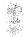
- FIG. 1 is an exploded perspective view of the relay 1.
- the relay 1 has a cover 2 and a main body 3.
- the cover 2 is attached to the main body 3 so as to cover the main body 3.
- the up and down directions in the present embodiment mean the up and down directions in FIG.
- the name of the direction in this embodiment is used for convenience of explanation, and does not limit the mounting direction of the relay 1 or the like.
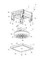
- FIG. 2 is an exploded perspective view of the main body 3 as viewed obliquely from above.
- FIG. 3 is an exploded perspective view of the main body portion 3 as viewed obliquely from below.
- the main body 3 has a base block 4, a movable block 5, and a coil block 6.
- the base block 4 supports the movable block 5 so as to be rotatable about the rotation axis Ra.
- the base block 4 has a base substrate 11.
- the base substrate 11 is disposed to face the movable block 5 in the direction of the rotation axis Ra of the movable block 5.
- the base substrate 11 has a square shape such as a square or a rectangle.
- the base block 4 is provided with a support portion 121.
- the support part 121 has a cylindrical shape.
- the support part 121 protrudes upward from the base substrate 11.
- the support part 121 supports the movable block 5 so that rotation is possible.
- the base substrate 11 has a plurality of contacts 13.
- the plurality of contacts 13 are formed of a conductive material.
- the base substrate 11 has 96 contacts 13. However, the number of the contacts 13 is not limited to 96, and may be less than 96 or more than 96.
- symbol is attached
- the plurality of contacts 13 are arranged around the support portion 121.
- the plurality of contacts 13 are arranged on the base substrate 11 on the radiation around the rotation axis Ra of the movable block 5.
- the plurality of contacts 13 are arranged on the base substrate 11 at intervals in the circumferential direction and the radial direction of the rotation of the movable block 5.
- the plurality of contacts 13 have a flat shape.
- the plurality of contacts 13 are provided on the surface of the base substrate 11.
- the surface of the base substrate 11 means a surface on which a plurality of contacts 13 are provided.
- the base substrate 11 has a plurality of terminal connection portions 14.
- the plurality of terminal connection portions 14 are provided on the back surface of the base substrate 11.
- the back surface of the base substrate 11 means a surface opposite to the surface on which the plurality of contacts 13 are provided.
- symbol is attached
- the surface of the base substrate 11 is disposed perpendicular to the rotation axis Ra.
- the back surface of the base substrate 11 is disposed perpendicular to the rotation axis Ra.
- the plurality of terminal connection portions 14 are arranged at the edge of the base substrate 11.
- the plurality of terminal connection portions 14 have a flat shape.
- the base substrate 11 is a so-called printed board.
- the plurality of contacts 13 and the plurality of terminal connection portions 14 are patterns formed on a printed board, and are formed of a conductor such as copper foil.
- the plurality of contacts 13 and the plurality of terminal connection portions 14 are not covered with an insulator and are exposed.
- a plurality of terminals may be attached to the plurality of terminal connection portions 14.
- the plurality of terminals may be linear terminals protruding from the base substrate 11. That is, the plurality of terminals may be surface-mounting terminals or through-hole terminals. Or a terminal may be comprised by BGA (Ball Grid Array) or LGA (Land Grid Array).
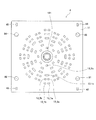
- FIG. 4 is a top view of the base block 4.
- FIG. 5 is a bottom view of the base block 4.
- the plurality of contacts 13 include a plurality of first contacts 13_1a and 13_2a, a plurality of second contacts 13_1b and 13_2b, and a plurality of third contacts 13_1c and 13_2c.
- the plurality of terminal connection portions 14 include a plurality of first terminal connection portions 14_1a and 14_2a, a plurality of second terminal connection portions 14_1b and 14_2b, and a plurality of third terminal connection portions 14_1c and 14_2c.
- symbol of the contactor 13 and the terminal connection part 14 has shown the contact structure.
- the plurality of first contacts are contacts constituting the a contact.
- a plurality of 2nd contactors are contacts which constitute b contact.
- a plurality of 3rd contactors are contacts which constitute c contact. 4 and 5, some of the plurality of first contacts (13_1a, 13_2a), some of the plurality of second contacts (13_1b, 13_2b), and some of the plurality of third contacts. Only (13_1c, 13_2c) is provided with reference numerals, and reference numerals of the other first contactors, second contactors, and third contactors are omitted.
- the first contact 13_1a and the second contact 13_1b are arranged at intervals in the circumferential direction in the rotation of the movable block 5.
- the first contact 13_1a and the third contact 13_1c are arranged at an interval in the radial direction in the rotation of the movable block 5.
- the third contact 13_1c is disposed closer to the rotation axis Ra than the first contact 13_1a and the second contact 13_1b.
- the first contact 13_2a and the second contact 13_2b are arranged at intervals in the circumferential direction in the rotation of the movable block 5.
- the first contact 13_2a and the third contact 13_2c are arranged at an interval in the radial direction in the rotation of the movable block 5.
- the third contact 13_2c is disposed closer to the rotation axis Ra than the first contact 13_2a and the second contact 13_2b.
- the base substrate 11 electrically connects a plurality of contacts 13 and a plurality of terminal connection portions 14.
- the first contact 13_1a and the first terminal connection portion 14_1a are connected.
- the second contact 13_1b and the second terminal connection portion 14_1b are connected.
- the third contact 13_1c and the third terminal connection portion 14_1c are connected.
- the first contact 13_2a and the first terminal connection portion 14_2a are connected.
- the second contact 13_2b and the second terminal connection portion 14_2b are connected.
- the third contact 13_2c and the third terminal connection portion 14_2c are connected.
- the other contactors 13 and the other terminal connection portions 14 are also electrically connected to each other on the base substrate 11 in the same manner.
- the plurality of second contacts may not be provided on a one-to-one basis with respect to the plurality of first contacts. That is, one second contact may be a common terminal for the plurality of first contacts. Similarly, the first contact may be a common terminal, or the third contact may be a common terminal.
- the movable block 5 is disposed on the base block 4. The movable block 5 is sandwiched between the base substrate 11 and the coil block 6.
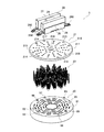
- FIG. 6 is an exploded perspective view of the movable block 5.
- FIG. 7 is a top view of the movable block 5.
- FIG. 8 is a bottom view of the movable block 5.
- the movable block 5 includes a rotating substrate 21, an armature 22, a plurality of sliders 23, and a holder 20.
- the rotating substrate 21 has a disk shape.
- the rotating substrate 21 is disposed to face the base substrate 11 in the direction of the rotation axis Ra.
- the plurality of sliders 23 are fixed to the rotating substrate 21.
- the movable block 5 has 64 sliders 23.
- the number of sliders 23 is not limited to 64, and may be less than 64 or more than 64.
- the plurality of sliders 23 are formed of a conductive material. Attached to the rotating substrate 21.
- the holder 20 is disposed between the rotating substrate 21 and the base substrate 11 in the direction of the rotation axis Ra.
- the holder 20 is fixed to the rotating substrate 21 and rotates together with the rotating substrate 21.
- the holder 20 has a plurality of through holes 91.
- the through hole 91 passes through the holder 20 in the direction of the rotation axis Ra.
- the through hole 91 has a slit shape and extends in the tangential direction of rotation of the movable block 5.
- a plurality of sliders 23 are respectively inserted into the plurality of through holes 91 of the holder 20. As shown in FIG. 3, the plurality of sliders 23 project downward from the holder 20 through the through holes 91 of the holder 20.
- the holder 20 is formed of an insulating material such as a resin.
- the movable block 5 has a rotating shaft 24.
- the rotation axis Ra described above is a center line of the rotation shaft 24.
- the rotating shaft 24 is provided on the lower surface of the holder 20.
- the lower surface of the holder 20 is a surface facing the surface of the base substrate 11.
- the rotating shaft 24 is supported by the support part 121 of the base block 4 described above.
- the rotating shaft 24 is disposed in the support portion 121. Therefore, the rotating shaft 24 is covered with the support portion 121. Thereby, it can suppress that the abrasion powder by rotation of the rotating shaft 24 scatters around.
- the plurality of sliders 23 are arranged at intervals in the circumferential direction and the radial direction of the rotation of the movable block 5.
- the plurality of sliders 23 are arranged on the radiation around the rotation axis Ra of the movable block 5.
- a plurality of mounting holes 211 are provided in the rotating substrate 21. In FIGS. 6 and 7, only a part of the plurality of mounting holes 211 is assigned a reference numeral, and the other attachment holes 211 are omitted.
- a plurality of sliders 23 are attached to the plurality of attachment holes 211.
- the rotating substrate 21 electrically connects a plurality of sliders 23.
- the rotating board 21 is a so-called printed board.
- the plurality of attachment holes 211 are through holes, and the plurality of attachment holes 211 are electrically connected by pattern wiring formed on the printed circuit board. Therefore, by attaching the slider 23 to the attachment hole 211, the plurality of sliders 23 are electrically connected to each other.
- the plurality of sliders 23 include a plurality of first sliders 23_1ab and 23_2ab and a plurality of second sliders 23_1c and 23_2c.
- the first slider 23_1ab and the second slider 23_1c are arranged at an interval in the radial direction in the rotation of the movable block 5.
- the second slider 23_1c is disposed closer to the rotation axis Ra than the first slider 23_1ab.
- the first slider 23_2ab and the second slider 23_2c are arranged at an interval in the radial direction in the rotation of the movable block 5.
- the second slider 23_2c is disposed closer to the rotation axis Ra than the first slider 23_2ab.
- the first slider 23_1ab and the second slider 23_1c are electrically connected to each other by the pattern wiring of the rotating substrate 21.
- the first slider 23_2ab, the second slider 23_2b, and the second slider 23_2c are also electrically connected to each other by the pattern wiring of the rotating substrate 21.
- FIG. 8 is a perspective view of the slider 23.
- FIG. 10 is an enlarged view of the slider 23 and the surrounding structure.
- the slider 23 has a thin plate shape. Specifically, the slider 23 has a flat shape along a plane perpendicular to the thickness direction of the slider 23.
- the slider 23 has a flat shape along the slit-like shape of the through hole 91 described above.
- the slider 23 is formed by electroforming, for example. However, the slider 23 may be formed by a manufacturing means other than electroforming.
- the slider 23 has a proximal end portion 38, a locking portion 39, a distal end portion 40, and a spring portion 41.
- the base end portion 38 protrudes from the holder 20 toward the rotary substrate 21 and is attached to the rotary substrate 21.
- the slider 23 is attached to the rotating substrate 21 by the base end portion 38 being press-fitted into the attachment hole 211.
- the base end portion 38 is provided with a slit 381. Thereby, when the base end part 38 is press-fitted into the mounting hole 211, the base end part 38 is elastically deformed.
- the base end portion 38 includes a first protrusion 382 and a second protrusion 383.
- the first protrusion 382 is locked to the surface of the rotating substrate 21 to prevent the slider 23 from coming off from the rotating substrate 21.
- the second projecting portion 383 is pressed into the mounting hole 211 to cut out a part of the through hole of the mounting hole 211. Thereby, the contact of the base end part 38 and a through hole is ensured.
- the locking portion 39 is larger than the base end portion 38 in the width direction of the slider 23.
- the width direction of the slider 23 means the left-right direction in FIG.
- the locking portion 39 is larger than the spring portion 41 in the width direction of the slider 23.
- the latching portion 39 regulates the movement of the slider 23 in the direction toward the base substrate 11 by latching to the holder 20.
- the through hole 91 includes a first hole portion 911, a second hole portion 912, and a step portion 913.
- the first hole portion 911 is larger than the locking portion 39 in a direction perpendicular to the rotation axis Ra direction.
- the first hole portion 911 is larger than the locking portion 39 in the width direction of the slider 23.
- the first hole 911 extends to the upper surface of the holder 20.
- the second hole portion 912 is smaller than the locking portion 39 in a direction perpendicular to the rotation axis Ra direction.
- the second hole portion 912 is smaller than the locking portion 39 in the width direction of the slider 23.
- the second hole portion 912 extends to the lower surface of the holder 20.
- a spring portion 41 is disposed in the second hole portion 912.
- the step portion 913 is provided between the first hole portion 911 and the second hole portion 912 and is locked to the locking portion 39.
- the tip 40 protrudes from the through hole 91 of the holder 20 toward the base substrate 11. As the movable block 5 rotates, the tip 40 slides on the base substrate 11 while being pressed against the base substrate 11. The distal end portion 40 is pressed against the contact 13 and comes into contact with the contact 13.
- the tip 40 has a tapered portion 401 and a straight portion 402.
- the taper portion 401 protrudes from the through hole 91 of the holder 20.
- the distance between the contact 13 ′ adjacent to the contact 13 in contact with the tip 40 in the circumferential direction of the rotation of the movable block 5 and the tip 40 is the contact 13 and the adjacent contact 13.
- the taper portion 401 has a tapered shape so as to be larger than the distance L1 between “′” and “′”.
- the straight portion 402 has a linear shape extending in the direction of the rotation axis Ra. At least a part of the linear portion 402 is disposed in the through hole 91.
- the linear portion 402 has a protruding portion 403 that protrudes toward the rotating substrate 21 side.
- the protrusion 403 increases the contact area between the inner surface of the through hole 91 and the tip 40.
- the spring portion 41 is provided between the distal end portion 40 and the proximal end portion 38.
- the spring part 41 is provided between the tip part 40 and the locking part 39.
- the spring portion 41 is disposed in the through hole 91 and has a bellows shape. In other words, the spring portion 41 has a shape that is folded back multiple times in the width direction of the slider 23. When the slider 23 is pressed against the base substrate 11, the spring portion 41 is compressed, and an elastic force is generated by the spring portion 41.
- the armature 22 is attached to the surface of the rotating substrate 21.
- the movable block 5 includes a support member 26 that supports the armature 22.
- the support member 26 is made of an insulating material such as resin.
- the armature 22 is attached to the rotating substrate 21 via a support member 26.
- the armature 22 includes a first armature 27, a second armature 28, and a permanent magnet 29.
- the first armature 27 and the second armature 28 are spaced from each other.
- the first armature 27 and the second armature 28 are arranged in parallel to each other.
- the first armature 27 and the second armature 28 are made of, for example, a semi-hard magnetic material. However, the first armature 27, the second armature 28, and the semi-hard magnetic material may be used.
- the permanent magnet 29 is disposed between the first armature 27 and the second armature 28.
- the permanent magnet 29 is disposed so as to overlap the rotation axis Ra when viewed from the direction of the rotation axis Ra.
- the rotation axis Ra is disposed between the first armature 27 and the second armature 28.
- the first armature 27 and the second armature 28 have an elongated shape.
- the armature 22 has a first recess 221 and a second recess 222. When viewed from the direction of the rotation axis Ra, the first recess 221 and the second recess 222 are arranged symmetrically with respect to the rotation axis Ra.
- the first recess 221 is constituted by one end of the first armature 27, one end of the second armature 28, and the permanent magnet 29.
- the second recess 222 is constituted by the other end of the first armature 27, the other end of the second armature 28, and the permanent magnet 29.
- the first recess 221 and the second recess 222 extend in the longitudinal direction of the first armature 27 and the second armature 28, respectively.
- FIG. 11 is a perspective view of the support member 26 as viewed obliquely from above.
- FIG. 12 is a perspective view of the support member 26 and the armature 22 as viewed obliquely from below.
- the support member 26 has a recess 31 in which the armature 22 is disposed.
- the support member 26 includes a first support part 32 and a second support part 33.
- the first armature 27 is disposed between the first support portion 32 and the second support portion 33.
- the support member 26 includes a third support part 34 and a fourth support part 35.
- the second armature 28 is disposed between the third support portion 34 and the fourth support portion 35.
- the first support portion 32 has a first protrusion 321.
- the second support part 33 has a second protrusion 331.
- the third support portion 34 has a third protrusion 341.
- the fourth support portion 35 has a fourth protrusion 351.
- the protrusions 321, 331, 341, 351 are arranged symmetrically with respect to the rotation axis Ra as viewed from the direction of the rotation axis Ra. When these protrusions 321, 331, 341, and 351 are pressed against the coil block 6, the support member 26 is sandwiched between the coil block 6 and the base substrate 11.
- a boss portion 25 is provided on the bottom surface of the support member 26.
- the boss portion 25 protrudes from the bottom surface of the support member 26.
- the boss portion 25 is disposed concentrically with the rotating shaft 24.
- a pair of openings 36 and 37 are arranged on both sides of the boss portion 25. The openings 36 and 37 penetrate the support member 26.
- the rotating substrate 21 has a through hole 210. The boss portion 25 of the support member 26 is inserted into the through hole 210.
- FIG. 12 a plurality of recesses 261 are provided on the bottom surface of the support member 26.
- a reference numeral 261 In FIG. 12, only a part of the plurality of recesses 261 is given a reference numeral 261, and the other recesses are omitted.
- the plurality of recesses 261 have a shape recessed upward from the bottom surface of the support member 26.
- FIG. 13 is a view of the movable block 5 as viewed from obliquely above. As shown in FIG. 13, the interference between the ends of the plurality of sliders 23 protruding from the surface of the rotating substrate 21 and the support member 26 is avoided by the plurality of recesses 261.
- the support member 26 has a plurality of fixing holes 262-265.
- the plurality of fixing holes 262-265 penetrate the support member 26.
- the support member 26 has first to fourth fixing holes 262-265.
- the first fixing hole 262 is disposed adjacent to the first support portion 32.
- the second fixing hole 263 is disposed adjacent to the second support portion 33.
- the third fixing hole 264 is disposed adjacent to the third support portion 34.
- the fourth fixing hole 265 is disposed adjacent to the fourth support portion 35.
- the rotary substrate 21 has a plurality of fixing holes 212-215.
- the plurality of fixing holes 212 to 215 penetrate the rotating substrate 21.
- the rotating substrate 21 has first to fourth fixing holes 212-215.
- the first to fourth fixing holes 212 to 215 of the rotating substrate 21 are provided corresponding to the first to fourth fixing holes 262-265 of the support member 26, respectively.
- the holder 20 has a plurality of fixing protrusions 92-95.
- the plurality of fixing protrusions 92-95 protrude from the upper surface of the holder 20.
- the plurality of fixing protrusions 92-95 are inserted into the plurality of fixing holes 262-265 of the support member 26 and the plurality of fixing holes 212-215 of the rotating substrate 21.
- the holder 20, the rotating substrate 21, and the support member 26 are integrally fixed by the plurality of fixing protrusions 92-95.
- the holder 20 has first to fourth fixing protrusions 92-95.
- the first to fourth fixing protrusions 92-95 are inserted into the first to fourth fixing holes 262-265 of the support member 26 and the first to fourth fixing holes 212-215 of the rotating substrate 21, respectively.
- the holder 20 has a plurality of locking projections 96-99.
- the plurality of locking protrusions 96-99 are shorter than the plurality of fixing protrusions 92-95.
- the rotating substrate 21 has a plurality of locking holes 216-219.
- the plurality of locking holes 216-219 are arranged corresponding to the plurality of locking protrusions 96-99.
- the plurality of locking holes 216-219 and the plurality of locking protrusions 96-99 are disposed at positions that do not face the support member 26.
- the plurality of locking projections 96-99 are inserted into the plurality of locking holes 216-219. As a result, the holder 20 is prevented from rotating with respect to the rotating substrate 21.
- the coil block 6 rotates the movable block 5 with respect to the base substrate 11.
- 14 and 15 are top views of the coil block 6 and the armature 22.
- the coil block 6 rotates the armature 22 from the position shown in FIG. 14 (hereinafter referred to as “first position”) in a predetermined direction (counterclockwise in FIGS. 14 and 15), so that the position shown in FIG. (Hereinafter referred to as “second position”). Further, the coil block 6 is moved to the first position shown in FIG. 14 by rotating the armature 22 from the second position shown in FIG. 15 in the direction opposite to the predetermined direction (clockwise in FIGS. 14 and 15). .
- FIG. 16 is an exploded perspective view of the coil block 6.
- the coil block 6 includes a first coil unit 51 and a second coil unit 52.
- the first coil unit 51 and the second coil unit 52 are arranged side by side in a direction perpendicular to the rotation axis Ra.
- the direction in which the first coil unit 51 and the second coil unit 52 are arranged is referred to as the width direction of the coil block 6.
- the first coil unit 51 includes a first coil bobbin 53, a first coil 54, and a first iron core 55.
- the first coil 54 is wound around the first coil bobbin 53.
- a first coil terminal 61 and a second coil terminal 62 are attached to the first coil bobbin 53.
- the first coil terminal 61 and the second coil terminal 62 are connected to the first coil 54.
- the first coil terminal 61 is connected to the first coil pad 42 of the base substrate 11 shown in FIG.
- the second coil terminal 62 is connected to the second coil pad 43 of the base substrate 11.
- the first iron core 55 is disposed in the hole 531 of the first coil bobbin 53.
- the first iron core 55 has a first end 551 and a second end 552.
- the first end portion 551 and the second end portion 552 of the first iron core 55 protrude from the first coil bobbin 53.
- the first iron core 55 is configured by laminating plate-like members having the same shape.
- the second coil unit 52 includes a second coil bobbin 63, a second coil 64, and a second iron core 65.
- the second coil 64 is disposed away from the first coil 54 in the width direction.
- the second coil bobbin 63 has the same shape as the first coil bobbin 53.
- a third coil terminal 71 and a fourth coil terminal 72 are attached to the second coil bobbin 63.
- the third coil terminal 71 and the fourth coil terminal 72 are connected to the second coil 64.
- the third coil terminal 71 is connected to the third coil pad 44 of the base substrate 11 shown in FIG.
- the fourth coil terminal 72 is connected to the fourth coil pad 45 of the base substrate 11.
- the second iron core 65 has the same shape as the first iron core 55.
- the second iron core 65 is disposed in the hole 631 of the second coil bobbin 63.
- the second iron core 65 has a first end 651 and a second end 652. The first end 651 and the second end 652 of the second iron core 65 protrude from the second coil bobbin 63.
- the coil block 6 includes a first connection yoke 56, a first yoke 57, a second connection yoke 58, and a second yoke 59.
- the first connecting yoke 56 is connected to the first end 551 of the first iron core 55 and the first end 651 of the second iron core 65.
- the first connection yoke 56 has a first opening 561 and a second opening 562. The first end 551 of the first iron core 55 is inserted into the first opening 561. The first end 651 of the second iron core 65 is inserted into the second opening 562.
- the first yoke 57 has a pair of support portions 571 and 572 and a tip portion 573.
- the first connection yoke 56 has a third opening 563 and a fourth opening 564.
- the pair of support portions 571 and 572 are inserted into the third opening 563 and the fourth opening 564, respectively.
- the distal end portion 573 protrudes toward the armature 22.
- the first yoke 57 is configured by laminating plate-like members having the same shape.
- the second connecting yoke 58 is connected to the second end 552 of the first iron core 55 and the second end 652 of the second iron core 65.
- the second connection yoke 58 has the same shape as the first connection yoke 56.
- the second connection yoke 58 has a first opening 581 and a second opening 582. The second end 552 of the first iron core 55 is inserted into the first opening 581. The second end 652 of the second iron core 65 is inserted into the second opening 582.
- the second yoke 59 has the same shape as the first yoke 57.
- the second yoke 59 has a pair of support parts 591, 592 and a tip part 593.
- the second connection yoke 58 has a third opening 583 and a fourth opening 584.
- the pair of support portions 591 and 592 are inserted into the third opening 583 and the fourth opening 584, respectively.
- the distal end portion 593 protrudes toward the armature 22.
- the first iron core 55, the second iron core 65, the first connection yoke 56, the first yoke 57, the second connection yoke 58, and the second yoke 59 are made of, for example, a semi-hard magnetic material. ing.
- the first protrusion 321 of the first support member 26 described above contacts and supports the support portion 571 of the first yoke 57.
- the second protrusion 331 contacts and supports the support portion 591 of the second yoke 59.
- the third protrusion 341 contacts and supports the support portion 572 of the first yoke 57.
- the fourth protrusion 351 contacts and supports the support portion 592 of the second yoke 59.
- the first coil 54 and the second coil 64 are arranged at a distance from each other.
- the armature 22 is disposed between the first coil 54 and the second coil 64.
- the first yoke 57 protrudes toward the armature 22 between the first coil 54 and the second coil 64.
- the second yoke 59 protrudes toward the armature 22 from the opposite side of the first yoke 57 between the first coil 54 and the second coil 64.
- the tip of the first yoke 57 is disposed in the first recess 221 of the armature 22.
- the tip of the second yoke 59 is disposed in the second recess 222 of the armature 22.
- the permanent magnet 29 and the rotation shaft 24 are disposed between the first yoke 57 and the second yoke 59. 17 and 18 show the flow of magnetic flux in the coil block 6. As shown in FIG.
- the first connecting yoke 56, the first yoke 57, the second armature 28, the permanent magnet 29, the first armature 27, the second yoke 59, and the second connecting yoke 58 are connected.
- a flow of magnetic flux that flows in sequence is generated. Therefore, as shown in FIG. 17, the magnetic flux of the first coil unit 51 and the magnetic flux of the second coil unit 52 overlap in the same direction in the armature 22, so that a large electromagnetic force acts on the armature 22.
- a large attractive force acts between the first armature 27 and the second yoke 59 and between the second armature 28 and the first yoke 57.
- the armature 22 rotates in a predetermined direction (counterclockwise in FIG. 17), and the movable block 5 also rotates in the predetermined direction.
- the armature 22 includes a first contact portion 223, a second contact portion 224, a third contact portion 225, and a fourth contact portion 226.
- the first contact portion 223 is an inner surface of one end portion of the first armature 27.
- the second contact portion 224 is an inner surface of the other end portion of the first armature 27.
- the third contact portion 225 is an inner surface of one end portion of the second armature 28.
- the fourth contact portion 226 is an inner surface of the other end portion of the second armature 28.
- one side surface 573a of the tip portion 573 of the first yoke 57 is inclined with respect to the longitudinal direction of the tip portion 573 so as to extend along the first contact portion 223 while being in contact with the first contact portion 223.
- the other side surface 573b of the tip portion 573 of the first yoke 57 is inclined with respect to the longitudinal direction of the tip portion 573 so as to extend along the third contact portion 225 while being in contact with the third contact portion 225. . That is, the side surface 573a and the side surface 573b are inclined so that the width of the front end portion 573 of the first yoke 57 increases toward the front end.
- one side surface 593a of the tip end portion 593 of the second yoke 59 is inclined with respect to the longitudinal direction of the tip end portion 593 so as to extend along the second contact portion 224 while being in contact with the second contact portion 224. is doing.
- the other side surface 593b of the tip portion 593 of the second yoke 59 is inclined with respect to the longitudinal direction of the tip portion 593 so as to extend along the fourth contact portion 226 in a state of being in contact with the fourth contact portion 226. . That is, the side surface 593a and the side surface 593b are inclined so that the width of the distal end portion 593 of the second yoke 59 increases toward the distal end.
- the coil block 6 is attached to the base substrate 11. As shown in FIG. 3, the coil block 6 has a plurality of fixing protrusions 73-76.
- the first coil bobbin 53 has a first fixed protrusion 73 and a second fixed protrusion 74.
- the first fixing protrusion 73 and the second fixing protrusion 74 are provided on the bottom surfaces of both end portions of the first coil bobbin 53.
- the second coil bobbin 63 has a third fixed protrusion 75 and a fourth fixed protrusion 76.
- the third fixing protrusion 75 and the fourth fixing protrusion 76 are provided on the bottom surfaces of both end portions of the second coil bobbin 63.
- the base block 4 is provided with a plurality of fixing holes 81-84.
- the plurality of fixing holes 81-84 are arranged corresponding to the plurality of fixing protrusions 73-76 of the coil block 6.
- the fixing protrusions 73-76 are inserted into these fixing holes 81-84, and are fixed by a fixing means such as an adhesive or cold welding.
- the movable block 5 is rotated with respect to the base substrate 11 so that the contact and disconnection between the slider 23 and the contact 13 are switched.
- the distal end portion 40 of the slider 23 corresponds to a movable contact
- the contact 13 corresponds to a fixed contact.
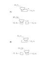
- FIG. 19 is a schematic diagram showing an arrangement of a part of the slider 23 and a part of the contact 13. Specifically, FIG. 19 shows the arrangement of the first and second sliders 23_1ab, 23_1c (see FIG. 9) and the first to third contacts 13_1a, 13_1b, 13_1c (see FIG. 4). Yes.
- the movable block 5 is located at the first position shown in FIG.
- FIG. 19B the movable block 5 is located at the second position shown in FIG.
- the first slider 23_1ab is in contact with the second contact 13_1b and not in contact with the first contact 13_1a. .
- the second slider 23_1c is in contact with the third contact 13_1c. Accordingly, the first slider 23_1ab is electrically connected to the second contact 13_1b and is not electrically connected to the first contact 13_1a. Accordingly, the second terminal connection portion 14_1b illustrated in FIG. 5 is connected to the third terminal connection portion 14_1c via the second contact 13_1b, the first slider 23_1ab, the second slider 23_1c, and the third contact 13_1c. And electrically connected. In addition, the first terminal connection portion 14_1a is electrically disconnected from the third terminal connection portion 14_1c.
- the movable block 5 When the movable block 5 rotates in a predetermined direction (counterclockwise in FIG. 19), the movable block 5 moves from the first position to the second position. As shown in FIG. 19B, when the movable block 5 is located at the second position, the first slider 23_1ab contacts the first contact 13_1a and does not contact the second contact 13_1b. The second slider 23_1c is in contact with the third contact 13_1c. Accordingly, the first slider 23_1ab is electrically connected to the first contact 13_1a and is not electrically connected to the second contact 13_1b.
- the first terminal connection portion 14_1a is electrically connected to the third terminal connection portion 14_1c via the first contact 13_1a, the first slider 23_1ab, the second slider 23_1c, and the third contact 13_1c. Connected.
- the second terminal connection portion 14_1b is electrically disconnected from the third terminal connection portion 14_1c.
- the first slider 23_1ab moves from the non-contact position to the contact position with respect to the first contact 13_1a. To do.
- the second slider 23_1c is always in contact with the third contact 13_1c. Further, along with the movement of the first and second sliders 23_1ab, 23_1b, and 23_1c described above, the other sliders also move. Accordingly, the plurality of first sliders are electrically connected to the plurality of first contacts and are not electrically connected to the plurality of second contacts.
- first and second sliders 23_1ab and 23_1c described above move, other sliders also move. Accordingly, the plurality of first sliders are brought out of conduction with the plurality of first contacts and are brought into conduction with the plurality of second contacts. Even when the coil block 6 is de-energized while the movable block 5 is in the first position, the movable block 5 is moved by the magnetic force of the permanent magnet 29 and the frictional force between each slider and the base substrate 11. Block 5 is held in the first position.
- the conduction state with the child can be switched alternately.
- the movable block 5 when the movable block 5 is rotated by the electromagnetic force of the coil block 6, the plurality of sliders 23 slide on the base substrate 11. Accordingly, the plurality of sliders 23 are moved to the contact positions with the plurality of contacts 13, whereby the plurality of sliders 23 and the plurality of contacts 13 are electrically connected. Further, the plurality of sliders 23 slide on the base substrate 11 and move to positions where the contacts 13 are not present, so that the plurality of sliders 23 and the plurality of contacts 13 become non-conductive. .
- the conductive state between the plurality of sliders 23 and the plurality of contacts 13 is switched by moving the plurality of sliders 23 while being in contact with the base substrate 11. For this reason, since a conduction
- the movable block 5 is sandwiched between the coil block 6 and the base block 4, the plurality of sliders 23 are pressed against the base substrate 11 by elastic force. Thereby, since the contact pressure between the slider 23 and the contact 13 is maintained, the contact reliability between the slider 23 and the contact 13 can be further improved.
- a large number of sliders 23 can be arranged in a small space on the rotating substrate 21, and a large number of contacts 13 can be arranged in a small space on the base substrate 11. For this reason, by increasing the number of the sliders 23 in the rotating substrate 21 and the number of the contacts 13 in the base substrate 11, the slider and the contacts that contribute to switching the conduction state while suppressing an increase in size. The number of sets (the number of contact poles) can be easily increased. Further, by changing the arrangement of the slider 23, the wiring pattern of the rotating substrate 21, and the wiring pattern of the base substrate 11, the number of contacts and contacts of the slider and the contact that contribute to switching of the conduction state The configuration can be changed.
- the sliders 23 By inserting the sliders 23 into the plurality of through holes 91 of the holder 20, the sliders 23 are supported by the holder 20 and the position of the sliders 23 can be regulated. Therefore, even when the thin slider 23 is used, the slider 23 can be prevented from falling or deforming when the movable block 5 is rotated.
- the slider 23 having a small plate thickness it is possible to suppress an excessive increase in the contact pressure between the slider 23 and the contact 13. Thereby, the electromagnetic force of the coil block 6 for driving the movable block 5 can be made small, and the enlargement of the coil block 6 can be suppressed.
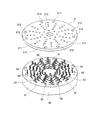
- FIG. 20 is a perspective view showing a state when the movable block 5 is manufactured.
- the direction of the plurality of sliders 23 is the longitudinal direction of the through holes 91, that is, the rotation of the holder 20. Aligned in the direction along the circumferential direction. Further, the base end portion 38 of the slider 23 protrudes from the upper surface of the holder 20.
- Insertion of the slider 23 into the plurality of through holes 91 of the holder 20 can be performed by, for example, an aligner. Since the slider 23 has the thin flat shape as described above, the slider 23 is less likely to be entangled with each other even if an aligner is used, and can be efficiently inserted into the plurality of through holes 91 of the holder 20. it can. Since the slider 23 is thin, the spring constant of the slider 23 can be reduced. Moreover, since the slider 23 has the spring part 41, the spring constant of the slider 23 can be made small. Accordingly, the slider 23 can be disposed in a space-saving manner, and the spring constant of the slider 23 can be reduced, so that the contact pressure between the slider 23 and the contact 13 can be reduced. Thereby, the movable block 5 can be rotationally driven with small electric power. Further, even if the assembly accuracy varies or the size of the slider 23 varies due to wear, a stable contact pressure can be secured.
- the contact configuration of the above embodiment has an a contact, a b contact, and a c contact, but only the a contact, only the b contact, only the c contact, or any combination of these contacts. It may be.
- the arrangement of the plurality of sliders 23 may be changed.
- the contacts 13 arranged corresponding to the sliders 23 are constituted by the two contacts 13 for one slider 23.
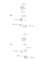
- the first contact 23_1ab and the first contact 13_1a form an a contact
- the slide 23_1ab and the second contact 13_1b form a b contact.
- the slider 23 and the contactor 13 may constitute the contact a and the contact b on a one-to-one basis.
- the first contact 23_1a and the first contact 13_1a form an a contact
- the second slide 23_1b and the second contact 13_1b form a b contact.
- the first slider 23_1a is not in contact with the first contact 13_1a
- the insulating layer of the base substrate 11 Touching when the movable block 5 is located at the first position, the first slider 23_1a is not in contact with the first contact 13_1a, and the insulating layer of the base substrate 11 Touching.
- the third slider 23_1c is in contact with the third contact 13_1c
- the second slider 23_1b is in contact with the second contact 13_1b. Accordingly, the second slider 23_1b and the second contact 13_1b are conductive, and the first slider 23_1a and the first contact 13_1a are non-conductive.
- the movable block 5 moves from the first position to the second position.
- the first slider 23_1a is in contact with the first contact 13_1a
- the third slider 23_1c is at the third contact. It is in contact with 13_1c.
- the second slider 23_1b is not in contact with the second contact 13_1b, but is in contact with the insulating layer of the base substrate 11. Accordingly, the first slider 23_1a and the first contact 13_1a are conductive, and the second slider 23_1b and the second contact 13_1b are non-conductive.
- the structure of the base block 4 is not limited to the structure of the above embodiment, and may be changed.
- the base substrate 11 is not limited to a quadrangle, and may have other shapes.
- the terminal connection part 14 of the base substrate 11 may be disposed at an arbitrary position. In this case, the position of the terminal connection portion 14 can be easily changed by changing the wiring pattern of the base substrate 11.
- the structure of the movable block 5 is not limited to the structure of the above embodiment, and may be changed.
- the first contact portion 223 and the second contact portion 224 of the contact may contact other portions of the coil block 6 without being limited to the first yoke 57 and the second yoke 59.
- the rotating substrate 21 is not limited to a disk shape, and may have another shape.
- the structure of the coil block 6 is not limited to the structure of the above embodiment, and may be changed.
- an integral coil that is not divided into the first coil 54 and the second coil 64 may be used.
- the rotating shaft 24 is provided in the holder 20, but may be provided in a component other than the holder 20.
- the rotating shaft 24 may be provided on the support member 26. In this case, the rotation shaft 24 may protrude from the support member 26 toward the base substrate 11 through holes provided in the rotation substrate 21 and the holder 20.
- the slider 23 is not limited to press-fitting but may be fixed to the rotating substrate 21 by other fixing means such as soldering.
- the shape of the slider 23 is not limited to the shape of the above-described embodiment, and may be changed.
- the shape of the base end portion 38 of the slider may be changed. 22 has a bulging portion 384 that is curved in the width direction.
- the bulging portion 384 is press-fitted into the mounting hole 211, so that the bulging portion 384 comes into pressure contact with the through hole of the mounting hole 211 by the elastic force of the bulging portion 384. Thereby, the contact of the base end part 38 and a through hole is ensured.
- the engaging part 39 of the slider may be changed.
- the locking portion 39 shown in FIG. 23 has a shape that is inclined so that the width of the locking portion 39 becomes wider toward the base end portion 38 side.
- the locking portion 39 is larger than the first hole portion 911 of the holder 20 in the width direction of the slider 23.
- the locking portion 39 is fixed to the holder 20 by being press-fitted into the first hole portion 911 of the holder 20.
- a bypass structure for shortening the transmission path length in the slider 23 may be provided in the slider 23.
- the slider 23 shown in FIG. 23 has a first bypass part 46 and a second bypass part 47.
- the first bypass portion 46 and the second bypass portion 47 have a linear shape extending from the base end portion 38 toward the tip end portion 40.
- the first bypass part 46 is connected to the base end part 38.
- the second bypass part 47 is connected to the tip part 40.
- the transmission path length between the first bypass part 46 and the second bypass part 47 is shorter than the transmission path length of the spring part 41.
- tip part 40 are electrically connected by the 1st bypass part 46 and the 2nd bypass part 47, and the transmission path length in the slider 23 is shortened.
- 23 includes a third bypass portion 48 and a fourth bypass portion 49.
- the third bypass part 48 is provided symmetrically with the first bypass part 46.
- the fourth bypass part 49 is provided symmetrically with the second bypass part 47. Also by the third bypass portion 48 and the fourth bypass portion 49, the base end portion 38 and the tip end portion 40 are electrically connected, and the transmission path length in the slider 23 is shortened.
- the number of contact poles can be increased while suppressing an increase in size, and a relay with high contact reliability can be provided.
Landscapes
- Physics & Mathematics (AREA)
- Electromagnetism (AREA)
- Micromachines (AREA)
Abstract
可動ブロックは、所定の回転軸線を中心に回転可能に設けられ、複数の摺動子と回転基板とホルダーとを有する。ベース基板は、可動ブロックの回転軸線方向に可動ブロックと対向して配置され、摺動子と接触する。ベース基板は、複数の摺動子と接触可能に配置される複数の接触子を有する。コイルブロックは、通電によって生じる電磁力によって、可動ブロックをベース基板に対して回転させるためのコイルを有する。回転基板には、複数の摺動子が固定されている。ホルダーは、回転軸線方向において回転基板とベース基板との間に配置される。ホルダーは、複数の摺動子が貫通している複数の貫通孔を有する。可動ブロックの回転に伴って、複数の摺動子と複数の接触子との導通状態が切り換わる。
Description
本発明は、リレーに関する。
リレーは、コイルと接極子とを有している。コイルが通電されることで生じる電磁力によって、接極子が動作する。これにより、接極子に設けられた可動接点と固定接点とのON/OFFが切り換えられる。
例えば、特許文献1のリレーでは、接極子が揺動可能に支持されており、接極子の両端に可動接触片が取り付けられている。コイルの電磁力によって接極子が揺動することにより、可動接触片が移動する。これにより、接点のON/OFFが切り換えられる。
例えば、特許文献1のリレーでは、接極子が揺動可能に支持されており、接極子の両端に可動接触片が取り付けられている。コイルの電磁力によって接極子が揺動することにより、可動接触片が移動する。これにより、接点のON/OFFが切り換えられる。
また、特許文献2のリレーでは、接極子がリンク部材を介して可動接触片に連結されている。コイルの電磁力によって接極子が回転すると、接極子の回転運動がリンク部材を介して直線運動に変換されて可動接触片に伝達される。これにより、接点のON/OFFが切り換えられる。
上述のリレーにおいて、接点の極数を増やすためには、可動接触片の数を増やす必要がある。可動接触片の数が増えると、可動接触片を支持するための構造が増大する。このため、リレーが大型化するという問題がある。
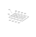
また、複数のリレーを組み合わせてリレーモジュールを構成することによって、極数を増やすことが考えられる。例えば、4極のリレーであれば、図25に示すように、8個のリレー200を基板300上に配置して組み合わせることにより、全体として32極のリレーモジュール100を構成することができる。しかし、この場合も、リレーモジュール全体としては大型化するという問題がある。また、複数のリレーを基板に、はんだ付けする必要があるため、製造工数が増えるという問題もある。
また、複数のリレーを組み合わせてリレーモジュールを構成することによって、極数を増やすことが考えられる。例えば、4極のリレーであれば、図25に示すように、8個のリレー200を基板300上に配置して組み合わせることにより、全体として32極のリレーモジュール100を構成することができる。しかし、この場合も、リレーモジュール全体としては大型化するという問題がある。また、複数のリレーを基板に、はんだ付けする必要があるため、製造工数が増えるという問題もある。
さらに、可動接触片と固定接点との接触圧力は、コイルの電磁力によって可動接触片が固定接点に押し付けられることによって得られる。この場合、接触圧力は、構成部品の寸法のバラツキによる影響を受け易い。例えば、可動接触片と固定接点との間の距離、或いは、リンク部材の長さなどのバラツキによって、接触圧力にバラツキが生じることが懸念される。従って、接点の接触信頼性を高めることは容易ではない。
本発明の課題は、大型化を抑えながら接点の極数を増やすことができると共に、接点の接触信頼性の高いリレーを提供することにある。
本発明の一態様に係るリレーは、可動ブロックと、ベース基板と、コイルブロックと、複数の接触子と、を備える。可動ブロックは、所定の回転軸線を中心に回転可能に設けられる。可動ブロックは、複数の摺動子を有する。ベース基板は、可動ブロックの回転軸線方向に可動ブロックと対向して配置され、摺動子と接触する。ベース基板は、複数の摺動子と接触可能に配置される複数の接触子を有する。コイルブロックは、コイルを有する。コイルは、通電によって生じる電磁力によって、可動ブロックをベース基板に対して回転させる。可動ブロックは、回転基板とホルダーとを有する。回転基板には、複数の摺動子が固定されている。ホルダーは、回転軸線方向において回転基板とベース基板との間に配置される。ホルダーは、複数の摺動子が貫通している複数の貫通孔を有する。可動ブロックの回転に伴って、複数の摺動子と複数の接触子との導通状態が切り換わる。
本態様に係るリレーでは、コイルブロックの電磁力によって可動ブロックが回転すると、複数の摺動子がベース基板上を摺動する。これにより、例えば、摺動子が接触子と接触する位置に移動することで、摺動子と接触子とが導通する。或いは、摺動子が、ベース基板上を摺動して、接触子が無い位置に移動することで、摺動子と接触子とが非導通になる。
このように、複数の摺動子がベース基板に接触した状態のまま移動することで、複数の摺動子と複数の接触子との導通状態が切り換えられる。すなわち、接触子の接触圧力を一定に保ちながら導通状態を切り換えることができるので、摺動子と接触子との接触信頼性を容易に向上させることができる。また、本態様に係るリレーでは、小さなスペースに多数の摺動子と接極子とを容易に配置することができる。このため、可動ブロックにおける摺動子の数と、ベース基板上における接触子の数とを増やすことで、大型化を抑えながら導通状態の切り換えに寄与する摺動子と接触子との組数を増やすことができる。
さらに、本態様に係るリレーでは、ホルダーの複数の貫通孔に摺動子がそれぞれ挿入されることで、摺動子が、ホルダーによって支持され、摺動子の位置を規制することができる。これにより、可動ブロックの回転時に、摺動子の倒れ、或いは変形を抑えることができるので、可動ブロックの動作安定性を向上させることができる。それにより、接触信頼性を高めることができる。また、可動ブロックの製造時に、ホルダーの複数の貫通孔に摺動子を挿入した状態で、複数の摺動子をまとめて回転基板に取り付けることができる。それにより、生産性を向上させることができる。
貫通孔は、スリット状であってもよい。摺動子は、貫通孔の形状に沿った平坦な形状を有してもよい。この場合、摺動子を貫通孔に挿入することで、自動的に摺動子の向きを揃えることができる。それにより、生産性をさらに向上させることができる。また、板厚の薄い摺動子を用いることによって、摺動子と接触子との接触圧力が過度に大きくなることを抑えることができる。これにより、可動ブロックを駆動するためのコイルブロックの電磁力を小さくすることができ、コイルブロックの大型化を抑えることができる。
摺動子は、摺動子の板厚方向に垂直な平面に沿った平坦な形状を有してもよい。この場合、摺動子が複雑に屈曲した形状である場合と比べて、摺動子を貫通孔に容易に挿入することができる。それにより、生産性をさらに向上させることができる。また、板厚の薄い摺動子を用いることによって、摺動子と接触子との接触圧力が過度に大きくなることを抑えることができる。これにより、可動ブロックを駆動するためのコイルブロックの電磁力を小さくすることができ、コイルブロックの大型化を抑えることができる。
貫通孔は、可動ブロックの回転の接線方向に延びた形状を有してもよい。この場合、摺動子が可動ブロックの回転の接線方向を向いて配置されるので、可動ブロックの回転時の摺動子と接触子との摩擦抵抗を低減することができる。それにより、小電力で可動ブロックを回転駆動することができる。
摺動子は、先端部と基端部とを有してもよい。先端部は、ホルダーからベース基板に向かって突出する。基端部は、ホルダーから回転基板に向かって突出し、回転基板に取り付けられる。
摺動子は、先端部と基端部とを有してもよい。先端部は、ホルダーからベース基板に向かって突出する。基端部は、ホルダーから回転基板に向かって突出し、回転基板に取り付けられる。
摺動子は、先端部と基端部との間に設けられるバネ部を有してもよい。バネ部は、貫通孔内に配置されてもよい。バネ部は、蛇腹状の形状を有してもよい。この場合、蛇腹状の形状によって、バネ部の展開長さを長くすることができる。これにより、摺動子を省スペースに配置することができると共に、摺動子のバネ定数が小さくなることで、摺動子と接触子との接触圧力を小さくすることができる。それにより、小電力で可動ブロックを回転駆動することができる。また、組立精度のバラツキ、或いは摺動子の磨耗による寸法のバラツキが生じても、安定的な接触圧力を確保することができる。
回転基板は、複数の取付孔を有してもよい。摺動子は、基端部が取付孔に圧入又は圧接されることで、回転基板に取り付けられてもよい。この場合、半田付けを省略することができるので、生産性をさらに向上させることができる。
複数の摺動子は、第1摺動子を有してもよい。複数の接触子は、第1接触子と、第1接触子に隣接する第2接触子と、を有してもよい。第2接触子と第1摺動子の先端部との間の距離が、第1接触子と第2接触子との間の距離よりも大きくなるように、第1接触子の先端部は先細りの形状を有してもよい。この場合、隣接する接触子からの絶縁距離を確保することができる。
複数の摺動子は、第1摺動子を有してもよい。複数の接触子は、第1接触子と、第1接触子に隣接する第2接触子と、を有してもよい。第2接触子と第1摺動子の先端部との間の距離が、第1接触子と第2接触子との間の距離よりも大きくなるように、第1接触子の先端部は先細りの形状を有してもよい。この場合、隣接する接触子からの絶縁距離を確保することができる。
摺動子は、ホルダーに係止する係止部を有してもよい。係止部がホルダーに係止することで、摺動子のベース基板側への移動が規制されてもよい。この場合、摺動子が回転基板に取り付けられるときに、係止部によって摺動子の移動が規制される。それにより、摺動子を回転基板に容易に取り付けることができる。バネ部は、先端部と係止部との間に設けられてもよい。
貫通孔は、第1孔部と、第2孔部と、段部と、を有してもよい。第1孔部は、回転軸線方向に垂直な方向において係止部よりも大きい。第2孔部は、回転軸線方向に垂直な方向において係止部よりも小さい。段部は、第1孔部と第2孔部との間に設けられ、係止部に係止する。この場合、第1孔部が係止部よりも大きいので、摺動子を回転基板に取り付けるときに、摺動子の位置を調整することができる。
可動ブロックは、ベース基板に対して回転可能に支持される回転軸を有してもよい。回転軸は、ホルダーに設けられてもよい。この場合、ホルダーに回転軸が設けられることで、ホルダーの貫通孔とベース基板の接触子との位置精度を向上させることができる。
可動ブロックは、ベース基板に対して回転可能に支持される回転軸を有してもよい。回転軸は、回転基板から、ホルダーに設けられた孔を通り、ベース基板に向かって突出していてもよい。この場合、回転軸を長くできるので、可動ブロックを安定的に回転させることができる。
可動ブロックは、ベース基板に対して回転可能に支持される回転軸を有してもよい。回転軸は、回転基板から、ホルダーに設けられた孔を通り、ベース基板に向かって突出していてもよい。この場合、回転軸を長くできるので、可動ブロックを安定的に回転させることができる。
複数の摺動子は、可動ブロックの回転の周方向と径方向とに互いに間隔をおいて配置されてもよい。複数の接触子は、ベース基板上において、可動ブロックの回転の周方向と径方向とに互いに間隔をおいて配置されてもよい。この場合、小さなスペースに数多くの摺動子と接触子とを配置することができる。
摺動子は、接触子と接触する接触位置と、接触子と接触しない非接触位置とに移動可能に設けられてもよい。コイルブロックが可動ブロックを回転させることにより、摺動子は、非接触位置と接触位置とに移動してもよい。
摺動子は、接触子と接触する接触位置と、接触子と接触しない非接触位置とに移動可能に設けられてもよい。コイルブロックが可動ブロックを回転させることにより、摺動子は、非接触位置と接触位置とに移動してもよい。
複数の摺動子は、第1摺動子を有してもよい。複数の接触子は、第1接触子と第2接触子とを有してもよい。摺動子は、第1接触子と接触する位置と、第2接触子と接触する位置とに移動可能に設けられてもよい。コイルブロックが可動ブロックを回転させることにより、第1摺動子は、第1接触子と接触する位置と、第2接触子と接触する位置とに移動してもよい。
本発明によれば、大型化を抑えながら接点の極数を増やすことができると共に、接点の接触信頼性の高いリレーを提供することができる。
以下、図面を参照して実施形態にかかるリレー1について説明する。図1は、リレー1の分解斜視図である。図1に示すように、リレー1は、カバー2と本体部3とを有する。カバー2は、本体部3を覆うように本体部3に取り付けられる。なお、本実施形態における上下の各方向は、それぞれ図1における上下の各方向を意味するものとする。ただし、本実施形態での方向の名称は、説明の便宜上用いるものであって、リレー1の取付方向等を限定するものではない。
図2は、本体部3を斜め上方から見た分解斜視図である。図3は、本体部3を斜め下方から見た分解斜視図である。図2及び図3に示すように、本体部3は、ベースブロック4と、可動ブロック5と、コイルブロック6とを有する。
ベースブロック4は、可動ブロック5を回転軸線Raを中心として回転可能に支持している。ベースブロック4は、ベース基板11を有する。ベース基板11は、可動ブロック5の回転軸線Ra方向に可動ブロック5と対向して配置される。
ベースブロック4は、可動ブロック5を回転軸線Raを中心として回転可能に支持している。ベースブロック4は、ベース基板11を有する。ベース基板11は、可動ブロック5の回転軸線Ra方向に可動ブロック5と対向して配置される。
ベース基板11は、正方形或いは長方形などの四角形状を有する。ベースブロック4には、支持部121が設けられている。支持部121は、筒状の形状を有している。支持部121は、ベース基板11から上方に突出している。支持部121は、可動ブロック5を回動可能に支持する。
ベース基板11は、複数の接触子13を有する。複数の接触子13は、導電性を有する材料で形成される。本実施形態では、ベース基板11は、96個の接触子13を有する。ただし、接触子13の数は、96に限らず、96より少ない、或いは96より多くてもよい。なお、図面においては、複数の接触子13の一部のみに符号を付して、他の接触子13の符号を省略している。
ベース基板11は、複数の接触子13を有する。複数の接触子13は、導電性を有する材料で形成される。本実施形態では、ベース基板11は、96個の接触子13を有する。ただし、接触子13の数は、96に限らず、96より少ない、或いは96より多くてもよい。なお、図面においては、複数の接触子13の一部のみに符号を付して、他の接触子13の符号を省略している。
複数の接触子13は、支持部121の周囲に配置されている。複数の接触子13は、ベース基板11上において、可動ブロック5の回転軸線Raを中心に放射線上に配置されている。複数の接触子13は、ベース基板11上において、可動ブロック5の回転の周方向と径方向とに互いに間隔をおいて配置される。複数の接触子13は、平坦な形状を有する。複数の接触子13は、ベース基板11の表面に設けられている。ベース基板11の表面とは、複数の接触子13が設けられている面を意味する。
図3に示すように、ベース基板11は、複数の端子接続部14を有する。複数の端子接続部14は、ベース基板11の裏面に設けられている。ベース基板11の裏面とは、複数の接触子13が設けられている面の反対の面を意味する。なお、図面においては、複数の端子接続部14の一部のみに符号を付して、他の端子接続部14の符号を省略している。
ベース基板11の表面は、回転軸線Raに対して垂直に配置される。ベース基板11の裏面は、回転軸線Raに対して垂直に配置される。複数の端子接続部14は、ベース基板11の縁部に配置されている。複数の端子接続部14は、平坦な形状を有する。
ベース基板11の表面は、回転軸線Raに対して垂直に配置される。ベース基板11の裏面は、回転軸線Raに対して垂直に配置される。複数の端子接続部14は、ベース基板11の縁部に配置されている。複数の端子接続部14は、平坦な形状を有する。
ベース基板11は、いわゆるプリント基板である。複数の接触子13と、複数の端子接続部14とは、プリント基板に形成されるパターンであり、銅箔などの導電体で形成される。複数の接触子13と複数の端子接続部14とは、絶縁体で被覆されておらず、露出している。
複数の端子接続部14には、複数の端子が取り付けられてもよい。複数の端子は、ベース基板11から突出する線状の端子であってもよい。すなわち、複数の端子は、表面実装用の端子であってもよく、或いは、スルーホール用の端子であってもよい。或いは、端子がBGA(Ball Grid Array)、或いはLGA(Land Grid Array)で構成されてもよい。
複数の端子接続部14には、複数の端子が取り付けられてもよい。複数の端子は、ベース基板11から突出する線状の端子であってもよい。すなわち、複数の端子は、表面実装用の端子であってもよく、或いは、スルーホール用の端子であってもよい。或いは、端子がBGA(Ball Grid Array)、或いはLGA(Land Grid Array)で構成されてもよい。
図4は、ベースブロック4の上面図である。図5は、ベースブロック4の底面図である。図4に示すように、複数の接触子13は、複数の第1接触子13_1a,13_2aと、複数の第2接触子13_1b,13_2bと、複数の第3接触子13_1c,13_2cとを有する。図5に示すように、複数の端子接続部14は、複数の第1端子接続部14_1a,14_2aと、複数の第2端子接続部14_1b,14_2bと、複数の第3端子接続部14_1c,14_2cとを有する。
なお、接触子13、及び端子接続部14の符号において“_”(アンダーバー)の後の符号は、接点構成を示している。後述するように、複数の第1接触子は、a接点を構成する接触子である。複数の第2接触子は、b接点を構成する接触子である。複数の第3接触子は、c接点を構成する接触子である。
なお、図4及び図5においては、複数の第1接触子の一部(13_1a,13_2a)、複数の第2接触子の一部(13_1b,13_2b)、及び複数の第3接触子の一部(13_1c,13_2c)、のみに符号を付しており、他の第1接触子、第2接触子、及び第3接触子の符号を省略している。
なお、図4及び図5においては、複数の第1接触子の一部(13_1a,13_2a)、複数の第2接触子の一部(13_1b,13_2b)、及び複数の第3接触子の一部(13_1c,13_2c)、のみに符号を付しており、他の第1接触子、第2接触子、及び第3接触子の符号を省略している。
図4に示すように、第1接触子13_1aと第2接触子13_1bとは、可動ブロック5の回転における周方向に間隔をおいて配置されている。第1接触子13_1aと第3接触子13_1cとは、可動ブロック5の回転における径方向に間隔をおいて配置されている。第3接触子13_1cは、第1接触子13_1a及び第2接触子13_1bよりも回転軸線Raの近くに配置される。
第1接触子13_2aと第2接触子13_2bとは、可動ブロック5の回転における周方向に間隔をおいて配置されている。第1接触子13_2aと第3接触子13_2cとは、可動ブロック5の回転における径方向に間隔をおいて配置されている。第3接触子13_2cは、第1接触子13_2a及び第2接触子13_2bよりも回転軸線Raの近くに配置される。
ベース基板11は、複数の接触子13と複数の端子接続部14とを電気的に接続している。例えば、第1接触子13_1aと第1端子接続部14_1aとが接続される。第2接触子13_1bと第2端子接続部14_1bとが接続される。第3接触子13_1cと第3端子接続部14_1cとが接続される。第1接触子13_2aと第1端子接続部14_2aとが接続される。第2接触子13_2bと第2端子接続部14_2bとが接続される。第3接触子13_2cと第3端子接続部14_2cとが接続される。詳細な説明は省略するが、他の接触子13及び他の端子接続部14についても同様に、それぞれベース基板11において互いに電気的に接続されている。
なお、複数の第1接触子に対して複数の第2接触子が1対1で設けられなくてもよい。すなわち、複数の第1接触子に対して1つの第2接触子がコモン端子となっていてもよい。同様に、第1接触子がコモン端子とされてもよく、或いは、第3接触子がコモン端子とされてもよい。
図1及び図2に示すように、可動ブロック5は、ベースブロック4上に配置されている。可動ブロック5は、ベース基板11とコイルブロック6との間に挟まれている。図6は、可動ブロック5の分解斜視図である。図7は、可動ブロック5の上面図である。図8は、可動ブロック5の底面図である。可動ブロック5は、回転基板21と、接極子22と、複数の摺動子23と、ホルダー20と、を有する。
図1及び図2に示すように、可動ブロック5は、ベースブロック4上に配置されている。可動ブロック5は、ベース基板11とコイルブロック6との間に挟まれている。図6は、可動ブロック5の分解斜視図である。図7は、可動ブロック5の上面図である。図8は、可動ブロック5の底面図である。可動ブロック5は、回転基板21と、接極子22と、複数の摺動子23と、ホルダー20と、を有する。
回転基板21は、円板状の形状を有する。回転基板21は、回転軸線Ra方向においてベース基板11に対向して配置される。
複数の摺動子23は、回転基板21に固定されている。本実施形態では、可動ブロック5は、64個の摺動子23を有する。ただし、摺動子23の数は、64に限らず、64より少ない、或いは、64より多くてもよい。複数の摺動子23は、導電性を有する材料で形成される。回転基板21に取り付けられている。
複数の摺動子23は、回転基板21に固定されている。本実施形態では、可動ブロック5は、64個の摺動子23を有する。ただし、摺動子23の数は、64に限らず、64より少ない、或いは、64より多くてもよい。複数の摺動子23は、導電性を有する材料で形成される。回転基板21に取り付けられている。
ホルダー20は、回転軸線Ra方向において回転基板21とベース基板11との間に配置される。ホルダー20は、回転基板21に固定されており、回転基板21と共に回転する。ホルダー20は、複数の貫通孔91を有する。貫通孔91は、回転軸線Ra方向にホルダー20を貫通している。貫通孔91は、スリット状であり、可動ブロック5の回転の接線方向に延びている。ホルダー20の複数の貫通孔91には、複数の摺動子23がそれぞれ挿入される。図3に示すように、複数の摺動子23は、ホルダー20の貫通孔91を通って、ホルダー20から下方に突出している。ホルダー20は、例えば樹脂などの絶縁性を有する材料で形成される。
図3及び図8に示すように、可動ブロック5は、回転軸24を有する。上述した回転軸線Raは、回転軸24の中心線である。図3に示すように、回転軸24は、ホルダー20の下面に設けられている。なお、ホルダー20の下面は、ベース基板11の表面と対向する面である。回転軸24は、上述したベースブロック4の支持部121に支持される。回転軸24は、支持部121内に配置される。従って、回転軸24が支持部121によって覆われる。これにより、回転軸24の回転による磨耗粉が周囲に飛散することを抑えることができる。
複数の摺動子23は、可動ブロック5の回転の周方向と径方向とに互いに間隔をおいて配置される。複数の摺動子23は、可動ブロック5の回転軸線Raを中心に放射線上に配置されている。
回転基板21には、複数の取付孔211が設けられている。なお、図6及び図7では、複数の取付孔211の一部のみに符号を付して他の取付孔211の符号を省略している。複数の取付孔211には、複数の摺動子23が取り付けられる。
回転基板21には、複数の取付孔211が設けられている。なお、図6及び図7では、複数の取付孔211の一部のみに符号を付して他の取付孔211の符号を省略している。複数の取付孔211には、複数の摺動子23が取り付けられる。
回転基板21は、複数の摺動子23を電気的に接続している。回転基板21は、いわゆるプリント基板である。複数の取付孔211は、スルーホールとなっており、プリント基板に形成されるパターン配線によって、複数の取付孔211が電気的に接続されている。従って、摺動子23が取付孔211に取り付けられることにより、複数の摺動子23が互いに電気的に接続される。
詳細には、図8に示すように、複数の摺動子23は、複数の第1摺動子23_1ab,23_2abと、複数の第2摺動子23_1c,23_2cと、を有する。第1摺動子23_1abと第2摺動子23_1cとは、可動ブロック5の回転における径方向に間隔をおいて配置されている。第2摺動子23_1cは、第1摺動子23_1abよりも回転軸線Raの近くに配置される。
第1摺動子23_2abと第2摺動子23_2cとは、可動ブロック5の回転における径方向に間隔をおいて配置されている。第2摺動子23_2cは、第1摺動子23_2abよりも回転軸線Raの近くに配置される。
第1摺動子23_1abと第2摺動子23_1cとは、回転基板21のパターン配線により互いに電気的に接続されている。第1摺動子23_2abと、第2摺動子23_2bと、第2摺動子23_2cも同様に、回転基板21のパターン配線により互いに電気的に接続されている。
第1摺動子23_1abと第2摺動子23_1cとは、回転基板21のパターン配線により互いに電気的に接続されている。第1摺動子23_2abと、第2摺動子23_2bと、第2摺動子23_2cも同様に、回転基板21のパターン配線により互いに電気的に接続されている。
なお、図8においては、複数の第1摺動子の一部(23_1ab,23_2ab)、及び複数の第2摺動子の一部(23_1c,23_2c)のみに符号を付して、他の第1摺動子及び第2摺動子の符号を省略している。詳細な説明は省略するが、他の第1摺動子及び第2摺動子についても同様に、それぞれパターン配線によって互いに接続されている。
図9は、摺動子23の斜視図である。図10は、摺動子23及びその周囲の構造の拡大図である。図9に示すように、摺動子23は、薄い板状の形状を有する。詳細には、摺動子23は、摺動子23の板厚方向に垂直な平面に沿った平坦な形状を有する。摺動子23は、上述した貫通孔91のスリット状の形状に沿った平坦な形状を有する。摺動子23は、例えば、電鋳により形成される。ただし、摺動子23は、電鋳以外の製造手段によって形成されてもよい。
図9は、摺動子23の斜視図である。図10は、摺動子23及びその周囲の構造の拡大図である。図9に示すように、摺動子23は、薄い板状の形状を有する。詳細には、摺動子23は、摺動子23の板厚方向に垂直な平面に沿った平坦な形状を有する。摺動子23は、上述した貫通孔91のスリット状の形状に沿った平坦な形状を有する。摺動子23は、例えば、電鋳により形成される。ただし、摺動子23は、電鋳以外の製造手段によって形成されてもよい。
摺動子23は、基端部38と、係止部39と、先端部40と、バネ部41と、を有する。基端部38は、ホルダー20から回転基板21に向かって突出し、回転基板21に取り付けられる。摺動子23は、基端部38が取付孔211に圧入されることで、回転基板21に取り付けられる。
詳細には、基端部38にはスリット381が設けられている。これにより、基端部38が取付孔211に圧入される際に、基端部38が弾性変形する。また、基端部38は、第1突出部382と第2突出部383とを有する。第1突出部382は、回転基板21の表面に係止することで、摺動子23を回転基板21に対して抜け止めする。第2突出部383は、取付孔211に圧入されることで、取付孔211のスルーホールの一部を削る。これにより、基端部38とスルーホールとの接触が確保される。
詳細には、基端部38にはスリット381が設けられている。これにより、基端部38が取付孔211に圧入される際に、基端部38が弾性変形する。また、基端部38は、第1突出部382と第2突出部383とを有する。第1突出部382は、回転基板21の表面に係止することで、摺動子23を回転基板21に対して抜け止めする。第2突出部383は、取付孔211に圧入されることで、取付孔211のスルーホールの一部を削る。これにより、基端部38とスルーホールとの接触が確保される。
係止部39は、摺動子23の幅方向において基端部38よりも大きい。なお、摺動子23の幅方向は、図10における左右方向を意味する。係止部39は、摺動子23の幅方向においてバネ部41よりも大きい。係止部39は、ホルダー20に係止することで、ベース基板11へ向かう方向への摺動子23の移動を規制する。
詳細には、貫通孔91は、第1孔部911と、第2孔部912と、段部913とを有する。第1孔部911は、回転軸線Ra方向に垂直な方向において係止部39よりも大きい。第1孔部911は、摺動子23の幅方向において係止部39よりも大きい。第1孔部911は、ホルダー20の上面まで延びている。第2孔部912は、回転軸線Ra方向に垂直な方向において係止部39よりも小さい。第2孔部912は、摺動子23の幅方向において係止部39よりも小さい。第2孔部912は、ホルダー20の下面まで延びている。第2孔部912内には、バネ部41が配置される。段部913は、第1孔部911と第2孔部912との間に設けられ、係止部39に係止する。
詳細には、貫通孔91は、第1孔部911と、第2孔部912と、段部913とを有する。第1孔部911は、回転軸線Ra方向に垂直な方向において係止部39よりも大きい。第1孔部911は、摺動子23の幅方向において係止部39よりも大きい。第1孔部911は、ホルダー20の上面まで延びている。第2孔部912は、回転軸線Ra方向に垂直な方向において係止部39よりも小さい。第2孔部912は、摺動子23の幅方向において係止部39よりも小さい。第2孔部912は、ホルダー20の下面まで延びている。第2孔部912内には、バネ部41が配置される。段部913は、第1孔部911と第2孔部912との間に設けられ、係止部39に係止する。
先端部40は、ホルダー20の貫通孔91からベース基板11に向かって突出している。可動ブロック5が回転することにより、先端部40は、ベース基板11に押し付けられた状態でベース基板11上を摺動する。先端部40は、接触子13に押し付けられ、接触子13と接触する。先端部40は、先細りのテーパ部401と直線部402とを有する。テーパ部401は、ホルダー20の貫通孔91から突出している。先端部40が接触している接触子13に、可動ブロック5の回転の周方向に隣接する接触子13’と先端部40との間の距離が、接触子13と、当該隣接する接触子13’との間の距離L1よりも大きくなるように、テーパ部401は先細りの形状を有する。
直線部402は、回転軸線Ra方向に延びる直線状の形状を有する。直線部402の少なくとも一部は、貫通孔91内に配置される。直線部402は、回転基板21側へ向かって突出する突起部403を有する。突起部403により貫通孔91の内面と先端部40との接触面積が増大する。
バネ部41は、先端部40と基端部38との間に設けられる。バネ部41は、先端部40と係止部39との間に設けられる。バネ部41は、貫通孔91内に配置され、蛇腹状の形状を有する。すなわち、バネ部41は、摺動子23の幅方向に複数回折り返された形状を有する。摺動子23がベース基板11に押し付けられることによりバネ部41が圧縮されて、バネ部41による弾性力が生じる。
バネ部41は、先端部40と基端部38との間に設けられる。バネ部41は、先端部40と係止部39との間に設けられる。バネ部41は、貫通孔91内に配置され、蛇腹状の形状を有する。すなわち、バネ部41は、摺動子23の幅方向に複数回折り返された形状を有する。摺動子23がベース基板11に押し付けられることによりバネ部41が圧縮されて、バネ部41による弾性力が生じる。
図2及び図7に示すように、接極子22は、回転基板21の表面に取り付けられる。詳細には、可動ブロック5は、接極子22を支持する支持部材26を有する。支持部材26は、樹脂などの絶縁性を有する材料で形成される。接極子22は、支持部材26を介して回転基板21に取り付けられる。
図7に示すように、接極子22は、第1接極子27と第2接極子28と永久磁石29とを有する。第1接極子27と第2接極子28とは互いに間隔をおいて配置されている。第1接極子27と第2接極子28とは、互いに平行に配置されている。第1接極子27と第2接極子28とは、例えば、半硬質磁性材料で形成されている。ただし、第1接極子27と第2接極子28と半硬質磁性材料と異なる材料で形成されてもよい。
図7に示すように、接極子22は、第1接極子27と第2接極子28と永久磁石29とを有する。第1接極子27と第2接極子28とは互いに間隔をおいて配置されている。第1接極子27と第2接極子28とは、互いに平行に配置されている。第1接極子27と第2接極子28とは、例えば、半硬質磁性材料で形成されている。ただし、第1接極子27と第2接極子28と半硬質磁性材料と異なる材料で形成されてもよい。
永久磁石29は、第1接極子27と第2接極子28との間に配置される。回転軸線Ra方向から見て、永久磁石29は、回転軸線Raと重なるように配置されている。回転軸線Ra方向から見て、回転軸線Raは、第1接極子27と第2接極子28との間に配置される。第1接極子27と第2接極子28とは、細長い形状を有している。
接極子22は、第1凹部221と第2凹部222とを有する。回転軸線Ra方向から見て、第1凹部221と第2凹部222とは、回転軸線Raを基準として対称に配置される。第1凹部221は、第1接極子27の一端と第2接極子28の一端と永久磁石29とによって構成される。第2凹部222は、第1接極子27の他端と第2接極子28の他端と永久磁石29とによって構成される。第1凹部221と第2凹部222とは、それぞれ第1接極子27と第2接極子28との長手方向に延びている。
接極子22は、第1凹部221と第2凹部222とを有する。回転軸線Ra方向から見て、第1凹部221と第2凹部222とは、回転軸線Raを基準として対称に配置される。第1凹部221は、第1接極子27の一端と第2接極子28の一端と永久磁石29とによって構成される。第2凹部222は、第1接極子27の他端と第2接極子28の他端と永久磁石29とによって構成される。第1凹部221と第2凹部222とは、それぞれ第1接極子27と第2接極子28との長手方向に延びている。
図11は、支持部材26を斜め上方から見た斜視図である。図12は、支持部材26と接極子22を斜め下方から見た斜視図である。支持部材26は、接極子22が配置される凹部31を有する。支持部材26は、第1支持部32と第2支持部33とを有する。第1支持部32と第2支持部33との間に第1接極子27が配置される。支持部材26は、第3支持部34と第4支持部35とを有する。第3支持部34と第4支持部35との間に第2接極子28が配置される。
第1支持部32は、第1突起321を有する。第2支持部33は、第2突起331を有する。第3支持部34は、第3突起341を有する。第4支持部35は、第4突起351を有する。図7に示すように、突起321,331,341,351は、回転軸線Ra方向から見て、回転軸線Raを基準に互いに対称に配置されている。これらの突起321,331,341,351がコイルブロック6に押圧されることにより、支持部材26がコイルブロック6とベース基板11とに挟持される。
図12に示すように、支持部材26の底面にはボス部25が設けられている。ボス部25は、支持部材26の底面から突出している。ボス部25は、回転軸24と同心に配置されている。ボス部25の両側方には一対の開口36,37が配置されている。開口36,37は、支持部材26を貫通している。図6に示すように、回転基板21は、貫通孔210を有している。支持部材26のボス部25は、貫通孔210に挿入される。
図12に示すように、支持部材26の底面には、複数の凹部261が設けられている。なお、図12では、複数の凹部261の一部のみに符号261を付して他の凹部の符号を省略している。複数の凹部261は、支持部材26の底面から上方に凹んだ形状を有する。図13は、可動ブロック5を斜め上方から見た図である。図13に示すように、複数の凹部261によって、回転基板21の表面から突出する複数の摺動子23の端部と支持部材26との干渉が回避される。
図11に示すように、支持部材26は、複数の固定孔262-265を有する。複数の固定孔262-265は、支持部材26を貫通している。詳細には、支持部材26は、第1~第4固定孔262-265を有する。第1固定孔262は、第1支持部32に隣接して配置される。第2固定孔263は、第2支持部33に隣接して配置される。第3固定孔264は、第3支持部34に隣接して配置される。第4固定孔265は、第4支持部35に隣接して配置される。
図6に示すように、回転基板21は、複数の固定孔212-215を有する。複数の固定孔212-215は、回転基板21を貫通している。詳細には、回転基板21は、第1~第4固定孔212-215を有する。回転基板21の第1~第4固定孔212-215は、それぞれ、支持部材26の第1~第4固定孔262-265に対応して設けられる。
ホルダー20は、複数の固定突起92-95を有する。複数の固定突起92-95は、ホルダー20の上面から突出している。複数の固定突起92-95は、支持部材26の複数の固定孔262-265と回転基板21の複数の固定孔212-215とに挿入される。複数の固定突起92-95によって、ホルダー20と回転基板21と支持部材26とが一体的に固定される。詳細には、ホルダー20は、第1~第4固定突起92-95を有する。第1~第4固定突起92-95は、それぞれ支持部材26の第1~第4固定孔262-265と回転基板21の第1~第4固定孔212-215とに挿入される。
ホルダー20は、複数の固定突起92-95を有する。複数の固定突起92-95は、ホルダー20の上面から突出している。複数の固定突起92-95は、支持部材26の複数の固定孔262-265と回転基板21の複数の固定孔212-215とに挿入される。複数の固定突起92-95によって、ホルダー20と回転基板21と支持部材26とが一体的に固定される。詳細には、ホルダー20は、第1~第4固定突起92-95を有する。第1~第4固定突起92-95は、それぞれ支持部材26の第1~第4固定孔262-265と回転基板21の第1~第4固定孔212-215とに挿入される。
ホルダー20は、複数の係止突起96-99を有する。複数の係止突起96-99は、複数の固定突起92-95よりも短い。回転基板21は、複数の係止孔216-219を有する。複数の係止孔216-219は、複数の係止突起96-99に対応して配置されている。複数の係止孔216-219と複数の係止突起96-99とは、支持部材26と対向しない位置に配置される。複数の係止突起96-99は、複数の係止孔216-219に挿入される。これにより、ホルダー20が回転基板21に対して回り止めされる。
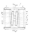
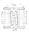
コイルブロック6は、可動ブロック5をベース基板11に対して回転させる。図14及び図15は、コイルブロック6及び接極子22の上面図である。コイルブロック6は、接極子22を図14に示す位置(以下、「第1位置」と呼ぶ)から所定方向(図14及び図15における反時計回り)に回転させることにより、図15に示す位置(以下、「第2位置」と呼ぶ)に移動させる。また、コイルブロック6は、接極子22を図15に示す第2位置から所定方向と逆方向(図14及び図15における時計回り)に回転させることにより、図14に示す第1位置に移動させる。
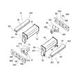
図16は、コイルブロック6の分解斜視図である。図16に示すように、コイルブロック6は、第1コイルユニット51と第2コイルユニット52とを有する。第1コイルユニット51と第2コイルユニット52とは、回転軸線Raに垂直な方向に並んで配置されている。以下、第1コイルユニット51と第2コイルユニット52とが並ぶ方向をコイルブロック6の幅方向と呼ぶ。
第1コイルユニット51は、第1コイルボビン53と、第1コイル54と、第1鉄芯55と、を有する。第1コイル54は第1コイルボビン53に巻回される。第1コイルボビン53には、第1コイル端子61と第2コイル端子62が取り付けられている。第1コイル端子61と第2コイル端子62とは、第1コイル54に接続されている。第1コイル端子61は、図4に示すベース基板11の第1コイルパッド42に接続される。第2コイル端子62は、ベース基板11の第2コイルパッド43に接続される。
第1鉄芯55は、第1コイルボビン53の孔531内に配置されている。第1鉄芯55は、第1端部551と第2端部552とを有する。第1鉄芯55の第1端部551と第2端部552とは、第1コイルボビン53から突出している。第1鉄芯55は、同一形状の板状の部材が積層されて構成されている。
第2コイルユニット52は、第2コイルボビン63と、第2コイル64と、第2鉄芯65と、を有する。第2コイル64は、第1コイル54から幅方向に離れて配置される。第2コイルボビン63は、第1コイルボビン53と同じ形状である。
第2コイルユニット52は、第2コイルボビン63と、第2コイル64と、第2鉄芯65と、を有する。第2コイル64は、第1コイル54から幅方向に離れて配置される。第2コイルボビン63は、第1コイルボビン53と同じ形状である。
第2コイルボビン63には、第3コイル端子71と第4コイル端子72が取り付けられている。第3コイル端子71と第4コイル端子72とは、第2コイル64に接続されている。第3コイル端子71は、図4に示すベース基板11の第3コイルパッド44に接続される。第4コイル端子72は、ベース基板11の第4コイルパッド45に接続される。
第2鉄芯65は、第1鉄芯55と同じ形状である。第2鉄芯65は、第2コイルボビン63の孔631内に配置されている。第2鉄芯65は、第1端部651と第2端部652とを有する。第2鉄芯65の第1端部651と第2端部652とは、第2コイルボビン63から突出している。
第2鉄芯65は、第1鉄芯55と同じ形状である。第2鉄芯65は、第2コイルボビン63の孔631内に配置されている。第2鉄芯65は、第1端部651と第2端部652とを有する。第2鉄芯65の第1端部651と第2端部652とは、第2コイルボビン63から突出している。
コイルブロック6は、第1連結ヨーク56と、第1ヨーク57と、第2連結ヨーク58と、第2ヨーク59と、を有する。第1連結ヨーク56は、第1鉄芯55の第1端部551と第2鉄芯65の第1端部651に接続される。第1連結ヨーク56は、第1開口561と第2開口562とを有する。第1開口561には、第1鉄芯55の第1端部551が挿入される。第2開口562には、第2鉄芯65の第1端部651が挿入される。
第1ヨーク57は、一対の支持部571,572と、先端部573とを有する。第1連結ヨーク56は、第3開口563と第4開口564とを有する。一対の支持部571,572は、それぞれ第3開口563と第4開口564とに挿入される。先端部573は、接極子22に向かって突出している。第1ヨーク57は、同一形状の板状の部材が積層されて構成されている。
第2連結ヨーク58は、第1鉄芯55の第2端部552と、第2鉄芯65の第2端部652に接続される。第2連結ヨーク58は、第1連結ヨーク56と同じ形状である。第2連結ヨーク58は、第1開口581と第2開口582とを有する。第1開口581には、第1鉄芯55の第2端部552が挿入される。第2開口582には、第2鉄芯65の第2端部652が挿入される。
第2ヨーク59は、第1ヨーク57と同じ形状である。第2ヨーク59は、一対の支持部591,592と、先端部593とを有する。第2連結ヨーク58は、第3開口583と第4開口584とを有する。一対の支持部591,592は、それぞれ第3開口583と第4開口584とに挿入される。先端部593は、接極子22に向かって突出している。
第1鉄芯55と、第2鉄芯65と、第1連結ヨーク56と、第1ヨーク57と、第2連結ヨーク58と、第2ヨーク59とは、例えば、半硬質磁性材料で形成されている。
なお、上述した第1支持部材26の第1突起321は、第1ヨーク57の支持部571に接触して支持する。第2突起331は、第2ヨーク59の支持部591に接触して支持する。第3突起341は、第1ヨーク57の支持部572に接触して支持する。第4突起351は、第2ヨーク59の支持部592に接触して支持する。
なお、上述した第1支持部材26の第1突起321は、第1ヨーク57の支持部571に接触して支持する。第2突起331は、第2ヨーク59の支持部591に接触して支持する。第3突起341は、第1ヨーク57の支持部572に接触して支持する。第4突起351は、第2ヨーク59の支持部592に接触して支持する。
図14及び図15に示すように、第1コイル54と第2コイル64とは、互いに間隔をおいて配置されている。接極子22は、第1コイル54と第2コイル64との間に配置される。第1ヨーク57は、第1コイル54と第2コイル64との間において接極子22に向かって突出する。第2ヨーク59は、第1コイル54と第2コイル64との間において第1ヨーク57と反対側から接極子22に向かって突出する。
第1ヨーク57の先端は、接極子22の第1凹部221内に配置される。第2ヨーク59の先端は、接極子22の第2凹部222内に配置される。回転軸線Ra方向から見て、永久磁石29と回転軸24とは、第1ヨーク57と第2ヨーク59との間に配置される。
図17及び図18は、コイルブロック6における磁束の流れを示している。図17に示すように、第1コイル54が通電されると、第1連結ヨーク56、第1ヨーク57、第2接極子28、永久磁石29、第1接極子27、第2ヨーク59、第2連結ヨーク58を順に流れる磁束の流れが生成される。
図17及び図18は、コイルブロック6における磁束の流れを示している。図17に示すように、第1コイル54が通電されると、第1連結ヨーク56、第1ヨーク57、第2接極子28、永久磁石29、第1接極子27、第2ヨーク59、第2連結ヨーク58を順に流れる磁束の流れが生成される。
また、第2コイル64が通電されると、第1連結ヨーク56、第1ヨーク57、第2接極子28、永久磁石29、第1接極子27、第2ヨーク59、第2連結ヨーク58を順に流れる磁束の流れが生成される。従って、図17に示すように、第1コイルユニット51の磁束と第2コイルユニット52の磁束とが接極子22において同方向に重なり合うことで、大きな電磁力が接極子22に作用する。これにより、第1接極子27と第2ヨーク59との間、及び第2接極子28と第1ヨーク57との間に大きな吸引力が作用する。その結果、接極子22が所定方向(図17における反時計回り)に回転し、それと共に可動ブロック5も所定方向に回転する。
また、第1コイル54及び第2コイル64への通電方向を上記と逆にすると、図18に示すように、第1コイルユニット51、第2コイルユニット52、及び接極子22における磁束の流れが、上記と逆になる。これにより、第1接極子27と第1ヨーク57との間、及び第2接極子28と第2ヨーク59との間に大きな吸引力が作用する。その結果、接極子22が所定方向と逆方向(図18における時計回り)に回転し、それと共に可動ブロック5も所定方向と逆方向に回転する。
図14及び図15に示すように、接極子22は、第1接触部223と第2接触部224と第3接触部225と第4接触部226とを有する。詳細には、第1接触部223は、第1接極子27の一方の端部の内側面である。第2接触部224は、第1接極子27の他方の端部の内側面である。第3接触部225は、第2接極子28の一方の端部の内側面である。第4接触部226は、第2接極子28の他方の端部の内側面である。
図15に示すように、接極子22が所定方向(図15における反時計回り)に回転すると、第1接触部223が、第1ヨーク57に接触する。また、第4接触部226が第2ヨーク59に接触する。これにより、接極子22の回転が規制される。従って、可動ブロック5が所定方向へ回転する場合、第1接触部223と第4接触部226とがコイルブロック6に接触することで、可動ブロック5の所定方向への回転量が規制される。
図14に示すように、接極子22が所定方向と逆方向(図14における時計回り)に回転すると、第2接触部224が、第2ヨーク59に接触する。また、第3接触部225が第1ヨーク57に接触する。これにより、接極子22の回転が規制される。従って、可動ブロック5が所定方向と逆方向へ回転する場合、第2接触部224と第3接触部225とがコイルブロック6に接触することで、可動ブロック5の所定方向への回転量が規制される。
なお、第1ヨーク57の先端部573の一方の側面573aは、第1接触部223と接触した状態で第1接触部223に沿って延びるように、先端部573の長手方向に対して傾斜している。第1ヨーク57の先端部573の他方の側面573bは、第3接触部225と接触した状態で第3接触部225に沿って延びるように、先端部573の長手方向に対して傾斜している。すなわち、第1ヨーク57の先端部573の幅が先端に向かって広がるように、側面573aと側面573bとが傾斜している。
同様に、第2ヨーク59の先端部593の一方の側面593aは、第2接触部224と接触した状態で第2接触部224に沿って延びるように、先端部593の長手方向に対して傾斜している。第2ヨーク59の先端部593の他方の側面593bは、第4接触部226と接触した状態で第4接触部226に沿って延びるように、先端部593の長手方向に対して傾斜している。すなわち、第2ヨーク59の先端部593の幅が先端に向かって広がるように、側面593aと側面593bとが傾斜している。
コイルブロック6は、ベース基板11に取り付けられる。図3に示すように、コイルブロック6は、複数の固定突起73-76を有している。詳細には、第1コイルボビン53は、第1固定突起73と第2固定突起74とを有している。第1固定突起73と第2固定突起74とは、第1コイルボビン53の両端部の底面に設けられる。第2コイルボビン63は、第3固定突起75と第4固定突起76とを有している。第3固定突起75と第4固定突起76とは、第2コイルボビン63の両端部の底面に設けられる。
ベースブロック4には、複数の固定孔81-84が設けられている。複数の固定孔81-84は、コイルブロック6の複数の固定突起73-76に対応して配置されている。固定突起73-76は、これらの固定孔81-84に挿入され、接着剤あるいは冷間圧接などの固定手段によって固定される。コイルブロック6がベース基板11に取り付けられることにより、可動ブロック5がベース基板11に向かって押圧される。
次に、本実施形態に係るリレー1における摺動子23と接触子13との導通状態の切換動作について説明する。本実施形態に係るリレー1では、可動ブロック5がベース基板11に対して回転することで、摺動子23と接触子13との接触と切断とが切り換えられる。本実施形態に係るリレー1では、摺動子23の先端部40が可動接点に相当し、接触子13が固定接点に相当する。摺動子23の先端部40が接触子13に接触することで、摺動子23が接触子13と導通する。すなわち、可動接点と固定接点とがON状態となる。摺動子23の先端部40が接触子13から離れることで、摺動子23が接触子13と非導通となる。すなわち、可動接点と固定接点とがOFF状態となる。
図19は、摺動子23の一部と接触子13の一部との配置を示す模式図である。詳細には、図19は、上述した第1,第2摺動子23_1ab,23_1c(図9参照)と第1~第3接触子13_1a,13_1b,13_1c(図4参照)との配置を示している。図19Aでは、可動ブロック5が図14に示す第1位置に位置している。図19Bでは、可動ブロック5が図15に示す第2位置に位置している。
図19Aに示すように、可動ブロック5が第1位置に位置しているときには、第1摺動子23_1abは、第2接触子13_1bと接触しており、第1接触子13_1aと接触していない。また、第2摺動子23_1cは、第3接触子13_1cと接触している。従って、第1摺動子23_1abは、第2接触子13_1bと導通しており、第1接触子13_1aとは非導通になっている。これにより、図5に示す第2端子接続部14_1bが、第2接触子13_1b、第1摺動子23_1ab、第2摺動子23_1c、第3接触子13_1cを介して、第3端子接続部14_1cと電気的に接続される。また、第1端子接続部14_1aは、第3端子接続部14_1cと電気的に切断される。
可動ブロック5が所定方向(図19における反時計周り)に回転すると、可動ブロック5は第1位置から第2位置に移動する。図19Bに示すように、可動ブロック5が第2位置に位置しているときには、第1摺動子23_1abは、第1接触子13_1aと接触し、第2接触子13_1bと接触していない。また、第2摺動子23_1cは、第3接触子13_1cと接触している。従って、第1摺動子23_1abは、第1接触子13_1aと導通しており、第2接触子13_1bとは非導通になっている。これにより、第1端子接続部14_1aが、第1接触子13_1a、第1摺動子23_1ab、第2摺動子23_1c、第3接触子13_1cを介して、第3端子接続部14_1cと電気的に接続される。また、第2端子接続部14_1bは、第3端子接続部14_1cと電気的に切断される。
以上のように、コイルブロック6が可動ブロック5を第1位置から第2位置に所定方向に回転させると、第1摺動子23_1abは、第1接触子13_1aに対する非接触位置から接触位置に移動する。第2摺動子23_1cは、第3接触子13_1cと常時接触している。
また、上述した第1,第2摺動子23_1ab,23_1b,23_1cの移動と共に、他の摺動子も移動する。これにより、複数の第1摺動子は、複数の第1接触子と導通すると共に、複数の第2接触子と非導通になる。
また、上述した第1,第2摺動子23_1ab,23_1b,23_1cの移動と共に、他の摺動子も移動する。これにより、複数の第1摺動子は、複数の第1接触子と導通すると共に、複数の第2接触子と非導通になる。
なお、可動ブロック5が第2位置に位置している状態で、コイルブロック6への通電が解除されても、永久磁石29の磁力及び各摺動子23とベース基板11との摩擦力により、可動ブロック5が第2位置に保持される。
可動ブロック5を所定方向と逆方向に回転させて第2位置から第1位置に移動させると、接点状態は、図19Bに示す状態から図19Aに示す状態に戻る。すなわち、第1摺動子23_1abは、第1接触子13_1aに対する接触位置から非接触位置に移動し、第2接触子13_1bに対する非接触位置から接触位置に移動する。第2摺動子23_1cは、第3接触子13_1cと常時接触している。
可動ブロック5を所定方向と逆方向に回転させて第2位置から第1位置に移動させると、接点状態は、図19Bに示す状態から図19Aに示す状態に戻る。すなわち、第1摺動子23_1abは、第1接触子13_1aに対する接触位置から非接触位置に移動し、第2接触子13_1bに対する非接触位置から接触位置に移動する。第2摺動子23_1cは、第3接触子13_1cと常時接触している。
また、上述した第1,第2摺動子23_1ab,23_1cの移動と共に、他の摺動子も移動する。これにより、複数の第1摺動子は、複数の第1接触子と非導通になると共に、複数の第2接触子と導通する。
なお、可動ブロック5が第1位置に位置している状態で、コイルブロック6への通電が解除されても、永久磁石29の磁力及び各摺動子とベース基板11との摩擦力により、可動ブロック5が第1位置に保持される。
なお、可動ブロック5が第1位置に位置している状態で、コイルブロック6への通電が解除されても、永久磁石29の磁力及び各摺動子とベース基板11との摩擦力により、可動ブロック5が第1位置に保持される。
以上のように、可動ブロック5の回転方向を切り換えることにより、複数のa接点と同等に機能する摺動子と接触子との導通状態と複数のb接点と同等に機能する摺動子と接触子との導通状態とを交互に切り換えることができる。
以上説明したように、本実施形態に係るリレー1では、コイルブロック6の電磁力によって可動ブロック5が回転すると、複数の摺動子23がベース基板11上を摺動する。これにより、複数の摺動子23が複数の接触子13との接触位置に移動することで、複数の摺動子23と複数の接触子13とが導通する。また、複数の摺動子23が、ベース基板11上を摺動して、接触子13が無い位置に移動することで、複数の摺動子23と複数の接触子13とが非導通になる。
以上説明したように、本実施形態に係るリレー1では、コイルブロック6の電磁力によって可動ブロック5が回転すると、複数の摺動子23がベース基板11上を摺動する。これにより、複数の摺動子23が複数の接触子13との接触位置に移動することで、複数の摺動子23と複数の接触子13とが導通する。また、複数の摺動子23が、ベース基板11上を摺動して、接触子13が無い位置に移動することで、複数の摺動子23と複数の接触子13とが非導通になる。
このように、複数の摺動子23がベース基板11に接触した状態のまま移動することで、複数の摺動子23と複数の接触子13との導通状態が切り換えられる。このため、摺動子23の接触圧力を一定に保ちながら導通状態を切り換えることができるので、摺動子23と接触子13との接触信頼性を容易に向上させることができる。特に、可動ブロック5がコイルブロック6とベースブロック4とに挟み込まれていることによって、複数の摺動子23が、弾性力によってベース基板11に押し付けられる。これにより、摺動子23と接触子13との接触圧力が維持されるので、摺動子23と接触子13との接触信頼性をさらに向上させることができる。
回転基板21上の小さなスペースに多数の摺動子23を配置することができる共に、ベース基板11上の小さなスペースに多数の接触子13を配置することができる。このため、回転基板21における摺動子23の数と、ベース基板11における接触子13の数とを増やすことで、大型化を抑えながら導通状態の切り換えに寄与する摺動子と接触子との組数(接点の極数)を容易に増やすことができる。また、摺動子23の配置と、回転基板21の配線パターンと、ベース基板11の配線パターンとを変更することで、導通状態の切り換えに寄与する摺動子と接触子との組数と接点構成とを変更することができる。
ホルダー20の複数の貫通孔91に摺動子23がそれぞれ挿入されることで、摺動子23が、ホルダー20によって支持され、摺動子23の位置を規制することができる。従って、板厚の薄い摺動子23を用いても、可動ブロック5の回転時に、摺動子23の倒れ、或いは変形を抑えることができる。
板厚の薄い摺動子23を用いることによって、摺動子23と接触子13との接触圧力が過度に大きくなることを抑えることができる。これにより、可動ブロック5を駆動するためのコイルブロック6の電磁力を小さくすることができ、コイルブロック6の大型化を抑えることができる。
板厚の薄い摺動子23を用いることによって、摺動子23と接触子13との接触圧力が過度に大きくなることを抑えることができる。これにより、可動ブロック5を駆動するためのコイルブロック6の電磁力を小さくすることができ、コイルブロック6の大型化を抑えることができる。
可動ブロック5の製造時に、ホルダー20の複数の貫通孔91に摺動子23を挿入した状態で、複数の摺動子23をまとめて回転基板21に取り付けることができる。それにより、生産性を向上させることができる。図20は、可動ブロック5の製造時の状態を示す斜視図である。図20に示すように、ホルダー20の複数の貫通孔91に摺動子23を挿入することによって、複数の摺動子23の向きが、貫通孔91の長手方向、すなわち、ホルダー20の回転の周方向に沿った向きに揃えられる。また、摺動子23の基端部38がホルダー20の上面から突出している。この状態で、回転基板21とホルダー20とを互いに押圧することで、摺動子23の基端部38が回転基板21の取付孔211に圧入される。これにより、複数の摺動子23をまとめて回転基板21に取り付けることができる。また、圧入によって、摺動子23が回転基板21に固定されるため、半田付けの工程を省略することができる。これにより、生産性を向上させることができる。
ホルダー20の複数の貫通孔91への摺動子23の挿入は、例えば整列機によって行うことができる。摺動子23が上述したような薄い平坦な形状であることにより、整列機を用いても摺動子23が互いに絡み合うことが少なく、ホルダー20の複数の貫通孔91に効率よく挿入することができる。
摺動子23の板厚が薄いため、摺動子23のバネ定数を小さくすることができる。また、摺動子23がバネ部41を有するため、摺動子23のバネ定数を小さくすることができる。これにより、摺動子23を省スペースに配置することができると共に、摺動子23のバネ定数が小さくなることで、摺動子23と接触子13との接触圧力を小さくすることができる。それにより、小電力で可動ブロック5を回転駆動することができる。また、組立精度のバラツキ、或いは摺動子23の磨耗による寸法のバラツキが生じても、安定的な接触圧力を確保することができる。
摺動子23の板厚が薄いため、摺動子23のバネ定数を小さくすることができる。また、摺動子23がバネ部41を有するため、摺動子23のバネ定数を小さくすることができる。これにより、摺動子23を省スペースに配置することができると共に、摺動子23のバネ定数が小さくなることで、摺動子23と接触子13との接触圧力を小さくすることができる。それにより、小電力で可動ブロック5を回転駆動することができる。また、組立精度のバラツキ、或いは摺動子23の磨耗による寸法のバラツキが生じても、安定的な接触圧力を確保することができる。
以上、本発明の一実施形態について説明したが、本発明は上記実施形態に限定されるものではなく、発明の要旨を逸脱しない範囲で種々の変更が可能である。
上記の実施形態の接点構成はa接点とb接点とc接点とを有しているが、a接点のみ、b接点のみ、c接点のみであってもよく、或いは、それらの接点の任意の組み合わせであってもよい。
上記の実施形態の接点構成はa接点とb接点とc接点とを有しているが、a接点のみ、b接点のみ、c接点のみであってもよく、或いは、それらの接点の任意の組み合わせであってもよい。
複数の摺動子23の配置は変更されてもよい。摺動子23に対応して配置される接触子13についても同様である。
上記の実施形態では1つの摺動子23に対して2つの接触子13によってa接点とb接点とが構成されている。例えば、第1摺動子23_1abと第1接触子13_1aとによってa接点が構成され、摺動子23_1abと第2接触子13_1bによってb接点が構成されている。しかし、摺動子23と接触子13とが1対1でa接点とb接点とをそれぞれ構成してもよい。
上記の実施形態では1つの摺動子23に対して2つの接触子13によってa接点とb接点とが構成されている。例えば、第1摺動子23_1abと第1接触子13_1aとによってa接点が構成され、摺動子23_1abと第2接触子13_1bによってb接点が構成されている。しかし、摺動子23と接触子13とが1対1でa接点とb接点とをそれぞれ構成してもよい。
例えば、図21に示すように、第1摺動子23_1aと第1接触子13_1aとによってa接点が構成され、第2摺動子23_1bと第2接触子13_1bとによってb接点が構成されてもよい。この場合、図21Aに示すように、可動ブロック5が第1位置に位置しているときには、第1摺動子23_1aは、第1接触子13_1aと接触しておらず、ベース基板11の絶縁層に接触している。また、第3摺動子23_1cは、第3接触子13_1cと接触しており、第2摺動子23_1bは、第2接触子13_1bと接触している。従って、第2摺動子23_1bと第2接触子13_1bとが導通しており、第1摺動子23_1a,と第1接触子13_1aとが非導通になっている。
可動ブロック5が所定方向(図21における反時計周り)に回転すると、可動ブロック5は第1位置から第2位置に移動する。図21Bに示すように、可動ブロック5が第2位置に位置しているときには、第1摺動子23_1aは、第1接触子13_1aと接触し、第3摺動子23_1cは、第3接触子13_1cと接触している。第2摺動子23_1bは、第2接触子13_1bと接触しておらず、ベース基板11の絶縁層に接触している。従って、第1摺動子23_1aと第1接触子13_1aとが導通しており、第2摺動子23_1bと第2接触子13_1bとが非導通になっている。
ベースブロック4の構造は、上記の実施形態の構造に限らず、変更されてもよい。例えば、ベース基板11は、四角形に限らず、他の形状であってもよい。ベース基板11の端子接続部14は、任意の位置に配置されてもよい。この場合、ベース基板11の配線パターンを変更することで、端子接続部14の位置を容易に変更することができる。
可動ブロック5の構造は、上記の実施形態の構造に限らず、変更されてもよい。例えば、接触子の第1接触部223と第2接触部224とは、第1ヨーク57と第2ヨーク59に限らず、コイルブロック6の他の部分に接触してもよい。回転基板21は、円板状に限らず、他の形状であってもよい。
可動ブロック5の構造は、上記の実施形態の構造に限らず、変更されてもよい。例えば、接触子の第1接触部223と第2接触部224とは、第1ヨーク57と第2ヨーク59に限らず、コイルブロック6の他の部分に接触してもよい。回転基板21は、円板状に限らず、他の形状であってもよい。
コイルブロック6の構造は、上記の実施形態の構造に限らず、変更されてもよい。例えば、第1コイル54と第2コイル64とに分割されていない一体のコイルが用いられてもよい。
上記の実施形態では、回転軸24はホルダー20に設けられているが、ホルダー20以外の部品に設けられてもよい。例えば、回転軸24が支持部材26に設けられてもよい。この場合、回転軸24は、支持部材26から、回転基板21及びホルダー20に設けられた孔を通り、ベース基板11に向かって突出してもよい。
上記の実施形態では、回転軸24はホルダー20に設けられているが、ホルダー20以外の部品に設けられてもよい。例えば、回転軸24が支持部材26に設けられてもよい。この場合、回転軸24は、支持部材26から、回転基板21及びホルダー20に設けられた孔を通り、ベース基板11に向かって突出してもよい。
摺動子23は、圧入に限らず、半田付けなどの他の固定手段によって回転基板21に固定されてもよい。摺動子23の形状は上述の実施形態の形状に限らず変更されてもよい。例えば、図22に示すように、摺動子の基端部38の形状が変更されてもよい。図22に示す基端部38は、幅方向に湾曲した膨出部384を有する。膨出部384は、取付孔211に圧入されることで、膨出部384の弾性力により取付孔211のスルーホールに圧接する。これにより、基端部38とスルーホールとの接触が確保される。
図23に示すように、摺動子の係止部39が変更されてもよい。図23に示す係止部39は、基端部38側に向かって係止部39の幅が広くなるように傾斜した形状を有する。係止部39は、摺動子23の幅方向においてホルダー20の第1孔部911よりも大きい。係止部39は、ホルダー20の第1孔部911に圧入されることでホルダー20に固定される。
図23に示すように、摺動子23における伝送経路長を短くするためのバイパス構造が摺動子23に設けられてもよい。図23に示す摺動子23は、第1バイパス部46と第2バイパス部47とを有する。第1バイパス部46と第2バイパス部47とは、基端部38から先端部40に向かって延びる直線状の形状を有する。第1バイパス部46は基端部38に接続されている。第2バイパス部47は先端部40に接続されている。第1バイパス部46と第2バイパス部47との伝送経路長は、バネ部41の伝送経路長よりも短い。摺動子23が自然状態では、第1バイパス部46と第2バイパス部47とは互いに乖離しているが、摺動子23がベース基板11に押し付けられて圧縮された状態では、互いに接触する。これにより、基端部38と先端部40とが第1バイパス部46と第2バイパス部47とによって電気的に接続され、摺動子23における伝送経路長が短縮される。また、図23に示す摺動子23は、第3バイパス部48と第4バイパス部49とを有する。第3バイパス部48は、第1バイパス部46と対称に設けられている。第4バイパス部49は、第2バイパス部47と対称に設けられている。第3バイパス部48と第4バイパス部49とによっても、基端部38と先端部40とが電気的に接続され、摺動子23における伝送経路長が短縮される。
本発明によれば、大型化を抑えながら接点の極数を増やすことができると共に、接点の接触信頼性の高いリレーを提供することができる。
23 摺動子
5 可動ブロック
13 接触子
11 ベース基板
6 コイルブロック
21 回転基板
20 ホルダー
40 先端部
38 基端部
41 バネ部
211 取付孔
39 係止部
911 第1孔部
912 第2孔部
913 段部
24 回転軸
5 可動ブロック
13 接触子
11 ベース基板
6 コイルブロック
21 回転基板
20 ホルダー
40 先端部
38 基端部
41 バネ部
211 取付孔
39 係止部
911 第1孔部
912 第2孔部
913 段部
24 回転軸
Claims (17)
- 所定の回転軸線を中心に回転可能に設けられ、複数の摺動子を有する可動ブロックと、
複数の前記摺動子と接触可能に配置される複数の接触子を有し、前記可動ブロックの回転軸線方向に前記可動ブロックと対向して配置され、前記摺動子と接触するベース基板と、
通電によって生じる電磁力によって、前記可動ブロックを前記ベース基板に対して回転させるためのコイルを有するコイルブロックと、
を備え、
前記可動ブロックは、
複数の前記摺動子が固定されている回転基板と、
前記回転軸線方向において前記回転基板と前記ベース基板との間に配置され、前記複数の摺動子が貫通している複数の貫通孔を有するホルダーと、
を有し、
前記可動ブロックの回転に伴って、複数の前記摺動子と複数の前記接触子との導通状態が切り換わることを特徴とするリレー。 - 前記貫通孔は、スリット状であり、
前記摺動子は、前記貫通孔の形状に沿った平坦な形状を有する、
請求項1に記載のリレー。 - 前記摺動子は、前記摺動子の板厚方向に垂直な平面に沿った平坦な形状を有する、
請求項1又は2に記載のリレー。 - 前記貫通孔は、前記可動ブロックの回転の接線方向に延びた形状を有する、
請求項2又は3に記載のリレー。 - 前記摺動子は、
前記ホルダーから前記ベース基板に向かって突出する先端部と、
前記ホルダーから前記回転基板に向かって突出し、前記回転基板に取り付けられる基端部と、
を有する、
請求項1から4のいずれかに記載のリレー。 - 前記摺動子は、前記先端部と前記基端部との間に設けられるバネ部を有し、
前記バネ部は、前記貫通孔内に配置されている、
請求項5に記載のリレー。 - 前記バネ部は、蛇腹状の形状を有する、
請求項6に記載のリレー。 - 前記回転基板は、複数の取付孔を有し、
前記摺動子は、前記基端部が前記取付孔に圧入又は圧接されることで、前記回転基板に取り付けられる、
請求項5から7のいずれかに記載のリレー。 - 複数の前記摺動子は、第1摺動子を有し、
複数の前記接触子は、第1接触子と、前記第1接触子に隣接する第2接触子と、を有し、
前記第2接触子と前記第1摺動子の先端部との間の距離が、前記第1接触子と前記第2接触子との間の距離よりも大きくなるように、前記第1接触子の先端部は先細りの形状を有する、
請求項5から8のいずれかに記載のリレー。 - 前記摺動子は、前記ホルダーに係止する係止部を有し、
前記係止部が前記ホルダーに係止することで、前記摺動子の前記ベース基板側への移動が規制され、
前記バネ部は、前記先端部と前記係止部との間に設けられる、
請求項6又は7に記載のリレー。 - 前記摺動子は、前記ホルダーに係止する係止部を有し、
前記係止部が前記ホルダーに係止することで、前記摺動子の前記ベース基板側への移動が規制される、
請求項1から9のいずれかに記載のリレー。 - 前記貫通孔は、
前記回転軸線方向に垂直な方向において前記係止部よりも大きな第1孔部と、
前記回転軸線方向に垂直な方向において前記係止部よりも小さな第2孔部と、
前記第1孔部と前記第2孔部との間に設けられ、前記係止部に係止する段部と、
を有する、
請求項10又は11に記載のリレー。 - 前記可動ブロックは、前記ベース基板に対して回転可能に支持される回転軸を有し、
回転軸は、前記ホルダーに設けられる、
請求項1から12のいずれかに記載のリレー。 - 前記可動ブロックは、前記ベース基板に対して回転可能に支持される回転軸を有し、
前記回転軸は、前記回転基板から、前記ホルダーに設けられた孔を通り、前記ベース基板に向かって突出する、
請求項1から13のいずれかに記載のリレー。 - 複数の前記摺動子は、前記可動ブロックの回転の周方向と径方向とに互いに間隔をおいて配置され、
複数の前記接触子は、前記ベース基板上において、前記可動ブロックの回転の周方向と径方向とに互いに間隔をおいて配置される、
請求項1から14のいずれかに記載のリレー。 - 前記摺動子は、前記接触子と接触する接触位置と、前記接触子と接触しない非接触位置とに移動可能に設けられ、
前記コイルブロックが前記可動ブロックを回転させることにより、前記摺動子は、前記非接触位置と前記接触位置とに移動する、
請求項1から15のいずれかに記載のリレー。 - 複数の前記接触子は、第1接触子と第2接触子とを有し、
前記摺動子は、前記第1接触子と接触する位置と、前記第2接触子と接触する位置とに移動可能に設けられ、
前記コイルブロックが前記可動ブロックを回転させることにより、前記摺動子は、前記第1接触子と接触する位置と、前記第2接触子と接触する位置とに移動する、
請求項1から15のいずれかに記載のリレー。
Applications Claiming Priority (2)
| Application Number | Priority Date | Filing Date | Title |
|---|---|---|---|
| JP2015-139183 | 2015-07-10 | ||
| JP2015139183A JP5880770B1 (ja) | 2015-07-10 | 2015-07-10 | リレー |
Publications (1)
| Publication Number | Publication Date |
|---|---|
| WO2017010017A1 true WO2017010017A1 (ja) | 2017-01-19 |
Family
ID=55453348
Family Applications (1)
| Application Number | Title | Priority Date | Filing Date |
|---|---|---|---|
| PCT/JP2015/072194 Ceased WO2017010017A1 (ja) | 2015-07-10 | 2015-08-05 | リレー |
Country Status (2)
| Country | Link |
|---|---|
| JP (1) | JP5880770B1 (ja) |
| WO (1) | WO2017010017A1 (ja) |
Cited By (1)
| Publication number | Priority date | Publication date | Assignee | Title |
|---|---|---|---|---|
| CN116705476A (zh) * | 2023-04-28 | 2023-09-05 | 厦门宏发电力电器有限公司 | 线圈架、磁路部分及继电器 |
Citations (2)
| Publication number | Priority date | Publication date | Assignee | Title |
|---|---|---|---|---|
| JPS54135638U (ja) * | 1978-03-14 | 1979-09-20 | ||
| JPS6349207U (ja) * | 1986-09-16 | 1988-04-04 |
-
2015
- 2015-07-10 JP JP2015139183A patent/JP5880770B1/ja active Active
- 2015-08-05 WO PCT/JP2015/072194 patent/WO2017010017A1/ja not_active Ceased
Patent Citations (2)
| Publication number | Priority date | Publication date | Assignee | Title |
|---|---|---|---|---|
| JPS54135638U (ja) * | 1978-03-14 | 1979-09-20 | ||
| JPS6349207U (ja) * | 1986-09-16 | 1988-04-04 |
Cited By (1)
| Publication number | Priority date | Publication date | Assignee | Title |
|---|---|---|---|---|
| CN116705476A (zh) * | 2023-04-28 | 2023-09-05 | 厦门宏发电力电器有限公司 | 线圈架、磁路部分及继电器 |
Also Published As
| Publication number | Publication date |
|---|---|
| JP5880770B1 (ja) | 2016-03-09 |
| JP2017022006A (ja) | 2017-01-26 |
Similar Documents
| Publication | Publication Date | Title |
|---|---|---|
| US9013253B2 (en) | Relay | |
| JP5991778B2 (ja) | 電磁継電器 | |
| US20100182111A1 (en) | Micro relay | |
| JP5720729B2 (ja) | 接点機構部 | |
| CN103311053B (zh) | 电磁继电器 | |
| JP2006523001A (ja) | 電磁リレー | |
| JP5880770B1 (ja) | リレー | |
| US6081176A (en) | Electromagnetic relay | |
| JP6922534B2 (ja) | 電磁継電器 | |
| JP5835510B1 (ja) | リレー | |
| JP4430487B2 (ja) | 対面型コネクタ | |
| WO2019026947A1 (ja) | 電磁継電器 | |
| JP4289301B2 (ja) | 電磁継電器 | |
| CN107210167B (zh) | 继电器 | |
| CN112582209A (zh) | 继电器 | |
| JP2017070206A (ja) | ステッピングモータ | |
| US6356174B1 (en) | Operator for an electromagnetic switching device | |
| US3258556A (en) | Electromagnetic actuator and relay comprising same | |
| WO2016157558A1 (ja) | 電磁継電器 | |
| KR200489019Y1 (ko) | 전자접촉기 | |
| JP4760400B2 (ja) | 電磁リレー | |
| JP2000306483A (ja) | 同軸リレー | |
| CN112582219B (zh) | 继电器 | |
| JP2008016215A (ja) | 電磁リレー | |
| KR102197518B1 (ko) | 전자 접촉기 |
Legal Events
| Date | Code | Title | Description |
|---|---|---|---|
| 121 | Ep: the epo has been informed by wipo that ep was designated in this application |
Ref document number: 15898329 Country of ref document: EP Kind code of ref document: A1 |
|
| NENP | Non-entry into the national phase |
Ref country code: DE |
|
| 122 | Ep: pct application non-entry in european phase |
Ref document number: 15898329 Country of ref document: EP Kind code of ref document: A1 |