WO2017006202A1 - 液晶表示装置および電子機器 - Google Patents
液晶表示装置および電子機器 Download PDFInfo
- Publication number
- WO2017006202A1 WO2017006202A1 PCT/IB2016/053727 IB2016053727W WO2017006202A1 WO 2017006202 A1 WO2017006202 A1 WO 2017006202A1 IB 2016053727 W IB2016053727 W IB 2016053727W WO 2017006202 A1 WO2017006202 A1 WO 2017006202A1
- Authority
- WO
- WIPO (PCT)
- Prior art keywords
- film
- oxide semiconductor
- transistor
- oxide
- liquid crystal
- Prior art date
- Legal status (The legal status is an assumption and is not a legal conclusion. Google has not performed a legal analysis and makes no representation as to the accuracy of the status listed.)
- Ceased
Links
Images

















Classifications
-
- G—PHYSICS
- G02—OPTICS
- G02F—OPTICAL DEVICES OR ARRANGEMENTS FOR THE CONTROL OF LIGHT BY MODIFICATION OF THE OPTICAL PROPERTIES OF THE MEDIA OF THE ELEMENTS INVOLVED THEREIN; NON-LINEAR OPTICS; FREQUENCY-CHANGING OF LIGHT; OPTICAL LOGIC ELEMENTS; OPTICAL ANALOGUE/DIGITAL CONVERTERS
- G02F1/00—Devices or arrangements for the control of the intensity, colour, phase, polarisation or direction of light arriving from an independent light source, e.g. switching, gating or modulating; Non-linear optics
- G02F1/01—Devices or arrangements for the control of the intensity, colour, phase, polarisation or direction of light arriving from an independent light source, e.g. switching, gating or modulating; Non-linear optics for the control of the intensity, phase, polarisation or colour
- G02F1/13—Devices or arrangements for the control of the intensity, colour, phase, polarisation or direction of light arriving from an independent light source, e.g. switching, gating or modulating; Non-linear optics for the control of the intensity, phase, polarisation or colour based on liquid crystals, e.g. single liquid crystal display cells
- G02F1/133—Constructional arrangements; Operation of liquid crystal cells; Circuit arrangements
-
- G—PHYSICS
- G02—OPTICS
- G02F—OPTICAL DEVICES OR ARRANGEMENTS FOR THE CONTROL OF LIGHT BY MODIFICATION OF THE OPTICAL PROPERTIES OF THE MEDIA OF THE ELEMENTS INVOLVED THEREIN; NON-LINEAR OPTICS; FREQUENCY-CHANGING OF LIGHT; OPTICAL LOGIC ELEMENTS; OPTICAL ANALOGUE/DIGITAL CONVERTERS
- G02F1/00—Devices or arrangements for the control of the intensity, colour, phase, polarisation or direction of light arriving from an independent light source, e.g. switching, gating or modulating; Non-linear optics
- G02F1/01—Devices or arrangements for the control of the intensity, colour, phase, polarisation or direction of light arriving from an independent light source, e.g. switching, gating or modulating; Non-linear optics for the control of the intensity, phase, polarisation or colour
- G02F1/13—Devices or arrangements for the control of the intensity, colour, phase, polarisation or direction of light arriving from an independent light source, e.g. switching, gating or modulating; Non-linear optics for the control of the intensity, phase, polarisation or colour based on liquid crystals, e.g. single liquid crystal display cells
- G02F1/133—Constructional arrangements; Operation of liquid crystal cells; Circuit arrangements
- G02F1/136—Liquid crystal cells structurally associated with a semi-conducting layer or substrate, e.g. cells forming part of an integrated circuit
- G02F1/1362—Active matrix addressed cells
- G02F1/136286—Wiring, e.g. gate line, drain line
-
- G—PHYSICS
- G02—OPTICS
- G02F—OPTICAL DEVICES OR ARRANGEMENTS FOR THE CONTROL OF LIGHT BY MODIFICATION OF THE OPTICAL PROPERTIES OF THE MEDIA OF THE ELEMENTS INVOLVED THEREIN; NON-LINEAR OPTICS; FREQUENCY-CHANGING OF LIGHT; OPTICAL LOGIC ELEMENTS; OPTICAL ANALOGUE/DIGITAL CONVERTERS
- G02F1/00—Devices or arrangements for the control of the intensity, colour, phase, polarisation or direction of light arriving from an independent light source, e.g. switching, gating or modulating; Non-linear optics
- G02F1/01—Devices or arrangements for the control of the intensity, colour, phase, polarisation or direction of light arriving from an independent light source, e.g. switching, gating or modulating; Non-linear optics for the control of the intensity, phase, polarisation or colour
- G02F1/13—Devices or arrangements for the control of the intensity, colour, phase, polarisation or direction of light arriving from an independent light source, e.g. switching, gating or modulating; Non-linear optics for the control of the intensity, phase, polarisation or colour based on liquid crystals, e.g. single liquid crystal display cells
- G02F1/133—Constructional arrangements; Operation of liquid crystal cells; Circuit arrangements
- G02F1/136—Liquid crystal cells structurally associated with a semi-conducting layer or substrate, e.g. cells forming part of an integrated circuit
- G02F1/1362—Active matrix addressed cells
- G02F1/1368—Active matrix addressed cells in which the switching element is a three-electrode device
-
- G—PHYSICS
- G09—EDUCATION; CRYPTOGRAPHY; DISPLAY; ADVERTISING; SEALS
- G09G—ARRANGEMENTS OR CIRCUITS FOR CONTROL OF INDICATING DEVICES USING STATIC MEANS TO PRESENT VARIABLE INFORMATION
- G09G3/00—Control arrangements or circuits, of interest only in connection with visual indicators other than cathode-ray tubes
- G09G3/20—Control arrangements or circuits, of interest only in connection with visual indicators other than cathode-ray tubes for presentation of an assembly of a number of characters, e.g. a page, by composing the assembly by combination of individual elements arranged in a matrix no fixed position being assigned to or needed to be assigned to the individual characters or partial characters
- G09G3/34—Control arrangements or circuits, of interest only in connection with visual indicators other than cathode-ray tubes for presentation of an assembly of a number of characters, e.g. a page, by composing the assembly by combination of individual elements arranged in a matrix no fixed position being assigned to or needed to be assigned to the individual characters or partial characters by control of light from an independent source
- G09G3/36—Control arrangements or circuits, of interest only in connection with visual indicators other than cathode-ray tubes for presentation of an assembly of a number of characters, e.g. a page, by composing the assembly by combination of individual elements arranged in a matrix no fixed position being assigned to or needed to be assigned to the individual characters or partial characters by control of light from an independent source using liquid crystals
-
- G—PHYSICS
- G09—EDUCATION; CRYPTOGRAPHY; DISPLAY; ADVERTISING; SEALS
- G09G—ARRANGEMENTS OR CIRCUITS FOR CONTROL OF INDICATING DEVICES USING STATIC MEANS TO PRESENT VARIABLE INFORMATION
- G09G3/00—Control arrangements or circuits, of interest only in connection with visual indicators other than cathode-ray tubes
- G09G3/20—Control arrangements or circuits, of interest only in connection with visual indicators other than cathode-ray tubes for presentation of an assembly of a number of characters, e.g. a page, by composing the assembly by combination of individual elements arranged in a matrix no fixed position being assigned to or needed to be assigned to the individual characters or partial characters
- G09G3/34—Control arrangements or circuits, of interest only in connection with visual indicators other than cathode-ray tubes for presentation of an assembly of a number of characters, e.g. a page, by composing the assembly by combination of individual elements arranged in a matrix no fixed position being assigned to or needed to be assigned to the individual characters or partial characters by control of light from an independent source
- G09G3/36—Control arrangements or circuits, of interest only in connection with visual indicators other than cathode-ray tubes for presentation of an assembly of a number of characters, e.g. a page, by composing the assembly by combination of individual elements arranged in a matrix no fixed position being assigned to or needed to be assigned to the individual characters or partial characters by control of light from an independent source using liquid crystals
- G09G3/3611—Control of matrices with row and column drivers
- G09G3/3648—Control of matrices with row and column drivers using an active matrix
-
- H—ELECTRICITY
- H10—SEMICONDUCTOR DEVICES; ELECTRIC SOLID-STATE DEVICES NOT OTHERWISE PROVIDED FOR
- H10D—INORGANIC ELECTRIC SEMICONDUCTOR DEVICES
- H10D30/00—Field-effect transistors [FET]
- H10D30/60—Insulated-gate field-effect transistors [IGFET]
- H10D30/67—Thin-film transistors [TFT]
-
- H—ELECTRICITY
- H10—SEMICONDUCTOR DEVICES; ELECTRIC SOLID-STATE DEVICES NOT OTHERWISE PROVIDED FOR
- H10D—INORGANIC ELECTRIC SEMICONDUCTOR DEVICES
- H10D86/00—Integrated devices formed in or on insulating or conducting substrates, e.g. formed in silicon-on-insulator [SOI] substrates or on stainless steel or glass substrates
- H10D86/40—Integrated devices formed in or on insulating or conducting substrates, e.g. formed in silicon-on-insulator [SOI] substrates or on stainless steel or glass substrates characterised by multiple TFTs
- H10D86/421—Integrated devices formed in or on insulating or conducting substrates, e.g. formed in silicon-on-insulator [SOI] substrates or on stainless steel or glass substrates characterised by multiple TFTs having a particular composition, shape or crystalline structure of the active layer
- H10D86/423—Integrated devices formed in or on insulating or conducting substrates, e.g. formed in silicon-on-insulator [SOI] substrates or on stainless steel or glass substrates characterised by multiple TFTs having a particular composition, shape or crystalline structure of the active layer comprising semiconductor materials not belonging to the Group IV, e.g. InGaZnO
-
- H—ELECTRICITY
- H10—SEMICONDUCTOR DEVICES; ELECTRIC SOLID-STATE DEVICES NOT OTHERWISE PROVIDED FOR
- H10D—INORGANIC ELECTRIC SEMICONDUCTOR DEVICES
- H10D86/00—Integrated devices formed in or on insulating or conducting substrates, e.g. formed in silicon-on-insulator [SOI] substrates or on stainless steel or glass substrates
- H10D86/40—Integrated devices formed in or on insulating or conducting substrates, e.g. formed in silicon-on-insulator [SOI] substrates or on stainless steel or glass substrates characterised by multiple TFTs
- H10D86/60—Integrated devices formed in or on insulating or conducting substrates, e.g. formed in silicon-on-insulator [SOI] substrates or on stainless steel or glass substrates characterised by multiple TFTs wherein the TFTs are in active matrices
-
- G—PHYSICS
- G02—OPTICS
- G02F—OPTICAL DEVICES OR ARRANGEMENTS FOR THE CONTROL OF LIGHT BY MODIFICATION OF THE OPTICAL PROPERTIES OF THE MEDIA OF THE ELEMENTS INVOLVED THEREIN; NON-LINEAR OPTICS; FREQUENCY-CHANGING OF LIGHT; OPTICAL LOGIC ELEMENTS; OPTICAL ANALOGUE/DIGITAL CONVERTERS
- G02F2201/00—Constructional arrangements not provided for in groups G02F1/00 - G02F7/00
- G02F2201/40—Arrangements for improving the aperture ratio
-
- G—PHYSICS
- G02—OPTICS
- G02F—OPTICAL DEVICES OR ARRANGEMENTS FOR THE CONTROL OF LIGHT BY MODIFICATION OF THE OPTICAL PROPERTIES OF THE MEDIA OF THE ELEMENTS INVOLVED THEREIN; NON-LINEAR OPTICS; FREQUENCY-CHANGING OF LIGHT; OPTICAL LOGIC ELEMENTS; OPTICAL ANALOGUE/DIGITAL CONVERTERS
- G02F2202/00—Materials and properties
- G02F2202/10—Materials and properties semiconductor
-
- G—PHYSICS
- G09—EDUCATION; CRYPTOGRAPHY; DISPLAY; ADVERTISING; SEALS
- G09G—ARRANGEMENTS OR CIRCUITS FOR CONTROL OF INDICATING DEVICES USING STATIC MEANS TO PRESENT VARIABLE INFORMATION
- G09G2300/00—Aspects of the constitution of display devices
- G09G2300/04—Structural and physical details of display devices
- G09G2300/0421—Structural details of the set of electrodes
- G09G2300/0426—Layout of electrodes and connections
-
- G—PHYSICS
- G09—EDUCATION; CRYPTOGRAPHY; DISPLAY; ADVERTISING; SEALS
- G09G—ARRANGEMENTS OR CIRCUITS FOR CONTROL OF INDICATING DEVICES USING STATIC MEANS TO PRESENT VARIABLE INFORMATION
- G09G2300/00—Aspects of the constitution of display devices
- G09G2300/04—Structural and physical details of display devices
- G09G2300/0439—Pixel structures
- G09G2300/0465—Improved aperture ratio, e.g. by size reduction of the pixel circuit, e.g. for improving the pixel density or the maximum displayable luminance or brightness
Definitions
- One embodiment of the present invention relates to a liquid crystal display device and an electronic device.
- one embodiment of the present invention is not limited to the above technical field.
- the technical field of the invention disclosed in this specification and the like relates to an object, a method, or a manufacturing method.
- one embodiment of the present invention relates to a process, a machine, a manufacture, or a composition (composition of matter). Therefore, the technical field of one embodiment of the present invention disclosed in this specification more specifically includes a semiconductor device, a display device, a light-emitting device, a power storage device, an imaging device, a memory device, a driving method thereof, or a driving method thereof.
- a manufacturing method can be mentioned as an example.
- Liquid crystal display devices are becoming increasingly commoditized. As one of the means for increasing added value, technological development of a liquid crystal display device that displays an ultra-high-definition image represented by a digital video format called “4K” or “8K” is active (for example, patents) References 1 and 2).
- An object of one embodiment of the present invention is to provide a novel liquid crystal display device or the like.
- Another object of one embodiment of the present invention is to provide a liquid crystal display device with a novel structure in which the number of data lines can be reduced and the aperture ratio can be improved.
- Another embodiment of the present invention is a liquid crystal display device having a novel structure that can perform good display even when a wiring material that transmits a signal to a pixel is formed using a material having a large parasitic resistance, such as a transparent conductive film. It is one of the issues to provide.
- Another object of one embodiment of the present invention is to provide a liquid crystal display device having a novel structure that can perform favorable display even when the amplitude of a video voltage transmitted to a pixel is reduced.
- One embodiment of the present invention includes a first pixel, a second pixel, a first wiring, a second wiring, a third wiring, and a fourth wiring.
- the pixel includes a first transistor and a first liquid crystal element
- the second pixel includes a second transistor and a second liquid crystal element
- the first transistor includes One of the source and the drain of the first transistor is electrically connected to the first wiring, and the other of the source and the drain of the first transistor is The first liquid crystal element is electrically connected, the first gate of the first transistor is electrically connected to the second wiring, and the second gate of the first transistor is connected to the third wiring.
- the second transistor is electrically connected and has a first gate and a second gate, and the second transistor One of the source and the drain of the transistor is electrically connected to the first wiring, and the other of the source and the drain of the second transistor is electrically connected to the second liquid crystal element, and the second transistor
- the first gate is electrically connected to the second wiring
- the second gate of the second transistor is electrically connected to the fourth wiring
- the first wiring transmits the video voltage to the first wiring.
- the second wiring has a function of transmitting a scanning signal to the first pixel and the second pixel
- the third wiring has a threshold value of the first transistor.
- the fourth wiring has a function of transmitting a first control signal for controlling the voltage, and the fourth wiring has a function of transmitting a second control signal for controlling the threshold voltage of the second transistor.
- the second transistor include a channel formation region.
- a liquid crystal display device is a transistor including an oxide semiconductor.
- the third wiring and the fourth wiring are preferably liquid crystal display devices having a function of transmitting light.
- the first gate of the first transistor has a region overlapping with the second gate of the first transistor with the channel formation region interposed therebetween, and the first gate of the second transistor A liquid crystal display device having a region overlapping with the second gate of the second transistor through the channel formation region is preferable.
- a liquid crystal display device in which the frequencies of the first control signal and the second control signal are smaller than the frequency of the scanning signal is preferable.
- a liquid crystal display device in which the voltage amplitude of the video voltage is smaller than the voltage amplitude of the first control signal or the second control signal is preferable.
- One embodiment of the present invention can provide a novel liquid crystal display device or the like.
- a liquid crystal display device having a novel structure in which the number of data lines can be reduced and the aperture ratio can be improved can be provided.
- Another embodiment of the present invention is a liquid crystal display device having a novel structure that can perform good display even when a wiring material that transmits a signal to a pixel is formed using a material having a large parasitic resistance, such as a transparent conductive film. Can be provided.
- a liquid crystal display device having a novel structure that can perform favorable display even when the amplitude of a video voltage transmitted to a pixel is reduced can be provided.
- the effects of one embodiment of the present invention are not limited to the effects listed above.
- the effects listed above do not preclude the existence of other effects.
- the other effects are effects not mentioned in this item described in the following description. Effects that are not mentioned in this item can be derived from descriptions of the specification or drawings by those skilled in the art, and can be appropriately extracted from these descriptions.
- one embodiment of the present invention has at least one of the effects listed above and / or other effects. Accordingly, one embodiment of the present invention may not have the above-described effects depending on circumstances.
- FIG. 10 is a circuit diagram illustrating one embodiment of the present invention.
- FIG. 10 is a circuit diagram illustrating one embodiment of the present invention.
- FIG. 10 is a circuit diagram illustrating one embodiment of the present invention.
- FIG. 10 is a circuit diagram illustrating one embodiment of the present invention.
- FIG. 10 is a circuit diagram illustrating one embodiment of the present invention.
- FIG. 10 is a circuit diagram illustrating one embodiment of the present invention.
- FIG. 10 is a circuit diagram illustrating one embodiment of the present invention.
- FIG. 10 is a circuit diagram illustrating one embodiment of the present invention.
- 6A and 6B are a circuit diagram and a timing chart for illustrating one embodiment of the present invention.
- FIG. 10 is a block diagram illustrating one embodiment of the present invention.
- FIG. 10 is a top view illustrating one embodiment of the present invention.
- FIG. 10 is a top view illustrating one embodiment of the present invention.
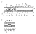
- FIG. 10 is a cross-sectional view illustrating one embodiment of the present invention.
- FIG. 10 is a top view illustrating one embodiment of the present invention.
- FIG. 10 is a top view illustrating one embodiment of the present invention.
- FIG. 10 is a cross-sectional view illustrating one embodiment of the present invention.
- 4A and 4B are a top view and a cross-sectional view illustrating an example of a liquid crystal display device. Sectional drawing which shows an example of a liquid crystal display device. Sectional drawing which shows an example of a liquid crystal display device.
- Sectional drawing which shows an example of a liquid crystal display device.
- the block diagram which shows an example of a touch panel module.
- the figure which shows an example of a touch panel module.
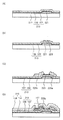
- Sectional drawing which shows an example of manufacturing methods, such as a transistor.
- Sectional drawing which shows an example of manufacturing methods, such as a transistor.
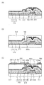
- Sectional drawing which shows an example of manufacturing methods, such as a transistor.
- Sectional drawing which shows an example of manufacturing methods, such as a transistor.
- FIG. 10 is a cross-sectional view illustrating an example of a transistor.
- 4A and 4B are a top view and cross-sectional views illustrating an example of a transistor.
- FIG. 10 is a cross-sectional view illustrating an example of a transistor. The figure explaining a band structure.
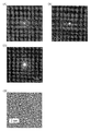
- FIGS. 6A and 6B illustrate a structural analysis by XRD of a CAAC-OS and a single crystal oxide semiconductor, and a diagram illustrating a limited field electron diffraction pattern of the CAAC-OS.
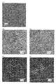
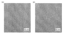
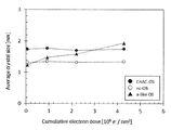
- FIG. 6 shows changes in crystal parts of an In—Ga—Zn oxide due to electron irradiation. The figure which shows an example of a touch panel module.
- FIG. 6 shows changes in crystal parts of an In—Ga—Zn oxide due to electron irradiation. The figure which shows an example of a touch panel module.
- FIG. 14 illustrates an example of an electronic device.
- FIG. 14 illustrates an example of an electronic device.
- the ordinal numbers “first”, “second”, and “third” are attached to avoid confusion between the constituent elements. Therefore, the number of components is not limited. Further, the order of the components is not limited. Further, for example, a component referred to as “first” in one embodiment of the present specification or the like is a component referred to as “second” in another embodiment or in the claims. It is also possible. Further, for example, the constituent elements referred to as “first” in one embodiment of the present specification and the like are omitted in the other embodiments or the claims.
- the liquid crystal display device has a plurality of pixels.
- two pixels 10_1 and 10_2 are typically shown.
- one pixel 10_1 may be an odd column pixel
- the other pixel 10_2 may be an even column pixel.
- the pixel 10_1 includes a transistor 11_1, a liquid crystal element CLC1, and a capacitor C S1 .
- Pixel 10_2 includes a transistor 11_2, a liquid crystal element C LC2, and a capacitance element C S2. Note that in the following description, the transistors 11_1 and 11_2 are n-channel transistors. Not limited to this, a p-channel transistor may be used.
- Transistors 11_1 and 11_2 have a back gate to which a signal for controlling a threshold voltage is applied in addition to a gate to which a signal for controlling a conduction state is applied.
- One of the source and the drain of the transistor 11_1 and one of the source and the drain of the transistor 11_2 are connected to the data line DL.
- the gate of the transistor 11_1 and the gate of the transistor 11_2 are connected to the gate line GL.
- the back gate of the transistor 11_1 is connected to the control line BGL_A.
- the back gate of the transistor 11_2 is connected to the control line BGL_B.
- a node to which the transistor 11_1 is connected to the liquid crystal element C LC1 and the capacitor element C S1 is referred to as a node N LC1 .
- a node to which the transistor 11_2 is connected to the liquid crystal element C LC2 and the capacitor element C S2 is referred to as a node N LC2 .
- a transmissive liquid crystal display device using a horizontal electric field liquid crystal element is described as an example.
- One electrode of the liquid crystal element C LC1 and the capacitor C S1 is connected to the transistor 11_1.
- the other electrodes of the liquid crystal element C LC1 and the capacitor element C S1 are connected to a wiring to which a common potential V COM is applied.
- one electrode of the liquid crystal element C LC2 and the capacitor element C S2 is connected to the transistor 11_2.
- the other electrodes of the liquid crystal element C LC2 and the capacitor element C S2 are connected to a wiring to which a common potential V COM is applied.
- a liquid crystal display device having a liquid crystal element as a display element will be described as an example, but the display element is not limited.
- Various elements such as optical elements using MEMS (Micro Electro Mechanical System), organic EL (Electro Luminescence) elements, light emitting diodes (LED: Light Emitting Diode), and electrophoretic elements are applied as display elements. be able to.
- MEMS Micro Electro Mechanical System
- organic EL Electro Luminescence
- LED Light Emitting Diode
- electrophoretic elements are applied as display elements. be able to.
- the data line DL has a function of transmitting a video voltage that is a voltage corresponding to data.
- the gate line GL has a function of transmitting a scanning signal for controlling the conduction state (or non-conduction state) of the transistor.
- the control lines BGL_A and BGL_B have a function of transmitting a control signal for controlling the threshold voltage of the transistor. Note that the data line DL, the gate line GL, and the control lines BGL_A and BGL_B may be simply referred to as wiring.
- FIG. 1B is a timing chart for explaining the operation of the circuit configuration shown in FIG.
- one frame (1F) is divided into two periods such as a first period and a second period, and a video voltage is written to the pixel 10_1 in the first period. In this period, a video voltage is written to the pixel 10_2.
- the pixels 10_1 and 10_2 are connected to the same data line DL and gate line GL.
- the threshold voltages of the transistors 11_1 and 11_2 are controlled so that the transistors 11_1 and 11_2 do not operate in the same manner by switching signals supplied to the control lines BGL_A and BGL_B. Then, the transistors 11_1 and 11_2 are controlled to be in a conductive state in different periods.
- a first period P1 for writing data to the pixel 10_1 and a second period P2 for writing data D2 to the pixel 10_2 are illustrated. Note that the timing chart in FIG. 1B illustrates changes in the scanning signal transmitted to the gate line GL, the video voltage transmitted to the data line DL, the control signals on the control lines BGL_A and BGL_B, and the nodes N LC1 and N LC2 .
- the scanning signal is illustrated with the H level as the voltage V GL_H and the L level as the voltage V GL_L .
- the video voltage is illustrated as being capable of taking a voltage according to the number of gradations between the voltage V D_H and the common potential V COM and between the voltage V D_L and the common potential V COM .
- the control signal is illustrated as a voltage V BG1 at the H level and a voltage V BG0 at the L level.
- FIG. 2A shows a circuit symbol of the transistor 11 having a back gate.
- the gate of the transistor 11 is connected to the gate line GL.
- One of the source and the drain of the transistor 11 is connected to the data line DL.
- the other of the source and the drain of the transistor 11 is connected to the node NLC .
- the back gate of the transistor 11 is connected to the control line BGL.
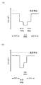
- FIG. 2B is a graph showing the relationship between the voltage V BGL applied to the control line BGL of the transistor 11 shown in FIG. 2A and the threshold voltage V TH of the transistor 11.
- V BG1 > V BG0 threshold voltage Vth1 corresponding to voltage V BG1 shifts negatively
- FIG. 2C is a diagram for explaining the shift of the threshold voltage in FIG. 2B in relation to the voltage V GL of the gate line GL and the drain current ID of the transistor 11.
- a curve 13_1 corresponds to a graph having a threshold voltage Vth1.
- a curve 13_0 corresponds to a graph having a threshold voltage of Vth0.
- the first period P1 illustrated in FIG. 1B includes a period in which the control signal of the control line BGL_A is set to the H level.
- the first period P1 illustrated in FIG. 1B includes a period in which the control signal of the control line BGL_B is set to the L level. Therefore, the threshold voltage of the transistor 11_1 is shifted to the negative side, and the threshold voltage of the transistor 11_2 is shifted to the positive side. Then, by setting the scanning signal to the H level, the transistor 11_1 whose threshold voltage is shifted to the negative side is turned on, and the transistor 11_2 whose threshold voltage is shifted to the positive side is turned off. When the transistor 11_1 conductive, the node N LC1 pixel 10_1 data D1 is written. Also when the transistor 11_2 nonconductive, the same data line DL, is connected to the gate line GL, the data D1 is not written into the node N LC2 pixel 10_2.
- the second period P2 illustrated in FIG. 1B there is a period in which the control signal of the control line BGL_B is at the H level.
- the second period P2 illustrated in FIG. 1B includes a period in which the control signal of the control line BGL_A is set to the L level. Therefore, the threshold voltage of the transistor 11_2 is shifted to the negative side, and the threshold voltage of the transistor 11_1 is shifted to the positive side. Then, by setting the scanning signal to the H level, the transistor 11_2 whose threshold voltage is shifted to the negative side is turned on, and the transistor 11_1 whose threshold voltage is shifted to the positive side is turned off.
- the node N LC2 pixel 10_2 data D2 is written. Also when the transistor 11_1 nonconductive, the same data line DL, is connected to the gate line GL, the data D2 is not written into the node N LC1 pixel 10_1. Therefore, the pixel 10_1 can continue to hold the data D1 written earlier.
- the frequency of the control signal applied to the back gate can be made lower than the frequency of the signal applied to the data line DL and the frequency of the scanning signal applied to the gate line GL. Therefore, a desired operation can be realized even if the parasitic capacitance or parasitic resistance of the control lines BGL_A and BGL_B is large.
- the wiring material forming the control lines BGL_A and BGL_B may have a large parasitic capacitance or resistance
- the wiring can be operated without using a low resistance material such as Cu or Al. .
- a wiring using a transparent conductive film such as an oxide conductive material can be used. Since a transparent wiring can be used for the pixel, it is possible to arrange the control lines BGL_A and BGL_B without impairing the aperture ratio even when the control lines BGL_A and BGL_B are added.
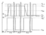
- FIG. 3 shows a timing chart for explaining the magnitude relationship between the scanning signal applied to the gate line GL, the video voltage applied to the data line DL, and the control signal applied to the control line BGL_A.
- the control signal applied to the control line BGL_A is described as an example, but the same applies to the control line BGL_B.
- a period P11 and a period P13 are periods in which the control line BGL_A is set to H level and the voltage of the data line DL is not written to the pixels.
- a period P12 is a period in which the control line BGL_A is set to L level and the data line DL This is the period during which the voltage is written to the pixel.
- the voltage applied to the back gate of the transistor is controlled to change the threshold voltage, thereby controlling the conduction state of the transistor. Therefore, the voltage applied to the back gate is a voltage that makes the transistor non-conductive regardless of the voltage of the scanning signal applied to the gate when the threshold voltage is shifted to the non-conductive state. For example, a voltage V BG0 the L level of the control line BGL_A that the threshold voltage plus the shift as a period P11 or P13 shown in FIG. 3, the voltage to be applied to other data lines DL and gate lines, reduced.
- the voltage applied to the back gate is a voltage that causes the transistor to become conductive in accordance with the voltage of the scanning signal applied to the gate when the threshold voltage is shifted by a minus shift.
- the H level voltage V BG1 of the control line BGL_A in which the threshold voltage is negatively shifted is larger than the voltage V BG0 and smaller than the voltage applied to the other data lines DL and gate lines. To do.
- the H level voltage V GL_H and the L level voltage V GL_L of the scanning signal applied to the gate line GL can be made larger than the voltage V BG1 .
- the video voltages V D_H and V D_L and the common potential V COM applied to the data line DL can be larger than the voltage V BG1 and between the voltage V GL_H and the voltage V GL_L .
- the video voltages V D_H and V D_L written to the pixels can be written in a state where the voltage applied to the back gate is set to the H level. Therefore, as shown in FIG.
- a video voltage can be written by applying a scanning signal of the gate line GL with a voltage amplitude equivalent to the voltage amplitude of the back gate voltage. That is, a video voltage can be written into the pixel with a small amplitude of the scanning signal voltage.
- the video voltage of the liquid crystal display device needs to be controlled by applying a sufficiently large voltage in order to perform inversion driving and to control conduction or non-conduction of the transistor.
- a voltage according to a control signal from the back gate is applied together with a voltage applied by a scanning signal. Therefore, even when the voltage amplitude of the video voltage and the scanning signal is lowered, the conduction / non-conduction of the transistor can be controlled. Therefore, since a video voltage and a voltage necessary for a scanning signal can be generated using an IC included in a display device having an organic EL or the like, the liquid crystal display device and the IC can be shared.
- the liquid crystal material constituting the liquid crystal element is preferably a material that can change the transmittance at a low voltage.
- ⁇ dielectric anisotropy
- a liquid crystal material having a large ⁇ may be selected and used as appropriate.
- the positive liquid crystal is more likely to have a difference in alignment state than the negative liquid crystal, and defects are likely to occur. This is because, when the interval between the slits provided in the electrodes of the liquid crystal element is small, the displacement of the alignment vector between adjacent liquid crystal molecules is large, and the increase in elastic energy due to bending strain is large.
- the elastic state can be made smaller in the orientation state formed by the spreading strain than when the elastic energy is increased by the bending strain, the bending strain is transferred to the spreading strain. Since the spreading distortion in the horizontal electric field method is close to the vertical alignment, the transmittance changes from a desired state.
- the orientation strain of the positive type liquid crystal can be divided into a spread strain term (K1), a deflection strain term (K2), and a bending strain term (K3).
- K1 a spread strain term
- K2 a deflection strain term
- K3 a bending strain term
- the spread distortion term (K1) is made larger than the bending distortion term (K3) by selecting a liquid crystal material.
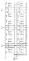
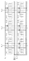
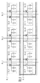
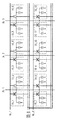
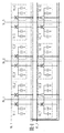
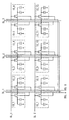
- FIG. 4 illustrates a circuit diagram of the pixels 10_1 to 10_12 in 2 rows and 6 columns in order to explain an example of the operation.
- the pixels 10_1 to 10_12 are connected to the data lines DL_1 to DL_3, the gate lines GL_1 to GL_2, the control line BGL_A, and the control line BGL_B, and data writing and the like are controlled.
- the transistors of the pixels in the odd columns are connected to the control line BGL_A.
- the transistors of the pixels in the even columns are connected to the control line BGL_B.
- FIGS. 5 to 8 show how data is written to the pixels when a signal is given to each wiring.
- the thick line is illustrated as a wiring to which an H level signal is applied
- the thin line is illustrated to be a wiring to which an L level signal is applied.
- FIG. 5 shows an operation of writing data to the pixels in the odd-numbered columns in the first row.
- a video signal is applied to the data lines DL_1 to DL_3 by setting the gate line scanning signal applied to the gate line GL_1 to the H level and the control signal applied to the control line BGL_A to the H level.
- Other wirings are at L level.
- Transistors included in the pixels 10_1, 10_3, and 10_5 are turned on. Even in the even-numbered column in the first row, an H level is applied by the scanning signal. However, since the control signal of the control line BGL_B is at the L level, the threshold voltages of the transistors included in the pixels 10_2, 10_4, and 10_6 are positively shifted.
- the transistors included in the pixels 10_2, 10_4, and 10_6 are turned off.
- the transistors included in the pixels in the second row are in a non-conduction state because the scanning signal of the gate line GL_2 is at L level regardless of the threshold voltage control by the control line BGL_A and the control line BGL_B.
- FIG. 6 shows an operation of writing data to the pixels in the odd-numbered columns in the second row.
- a video signal is applied to the data lines DL_1 to DL_3 by setting the scanning signal of the gate line applied to the gate line GL_2 to the H level and the control signal applied to the control line BGL_A to the H level.
- Other wirings are at L level.
- Transistors included in the pixels 10_7, 10_9, and 10_11 are turned on. Even in the second column, the H level is applied by the scanning signal. However, since the control signal of the control line BGL_B is at the L level, the threshold voltages of the transistors included in the pixels 10_8, 10_10, and 10_12 are positively shifted.
- the transistors included in the pixels 10_8, 10_10, and 10_12 are turned off.
- the transistors included in the pixels in the first row are in a non-conductive state because the scanning signal of the gate line GL_1 is L level regardless of the threshold voltage control by the control line BGL_A and the control line BGL_B.
- FIG. 7 shows an operation of writing data to the pixels in the even-numbered columns in the first row.
- a video voltage is applied to the data lines DL_1 to DL_3 by setting the scanning signal of the gate line applied to the gate line GL_1 to the H level and the control signal applied to the control line BGL_B to the H level.
- Other wirings are at L level.
- Transistors included in the pixels 10_2, 10_4, and 10_6 are turned on.
- the odd-numbered column in the first row is also applied with the H level by the scanning signal.
- the control signal of the control line BGL_A is at the L level, the threshold voltages of the transistors included in the pixels 10_1, 10_3, and 10_5 are positively shifted.
- the transistors included in the pixels 10_1, 10_3, and 10_5 are turned off.
- the transistors included in the pixels in the second row are in a non-conduction state because the scanning signal of the gate line GL_2 is at L level regardless of the threshold voltage control by the control line BGL_A and the control line BGL_B.
- FIG. 8 shows an operation of writing data to the pixels in the even-numbered columns in the second row.
- a video voltage is applied to the data lines DL_1 to DL_3 by setting the scanning signal of the gate line applied to the gate line GL_2 to the H level and the control signal applied to the control line BGL_B to the H level.
- Other wirings are at L level.
- Transistors included in the pixels 10_8, 10_10, and 10_12 are turned on.
- the odd-numbered column in the second row is also applied with the H level by the scanning signal.
- the control signal of the control line BGL_A is at the L level, the threshold voltages of the transistors included in the pixels 10_7, 10_9, and 10_11 are positively shifted.
- the transistors included in the pixels 10_7, 10_9, and 10_11 are turned off.
- the transistors included in the pixels in the first row are in a non-conductive state because the scanning signal of the gate line GL_1 is L level regardless of the threshold voltage control by the control line BGL_A and the control line BGL_B.
- the pixels of the liquid crystal display device whose operation has been described with reference to FIGS. 5 to 8 can selectively control the writing of data to the pixels when connected to the same data line and gate line. Therefore, wiring for writing data to the pixel can be reduced.
- the control signal for controlling the threshold voltage of the transistor can be a signal that is switched at a cycle of 1 ⁇ 2 frame. For this reason, a signal having a lower frequency than signals given to other wirings is handled. In the case of a signal having a low frequency, even if a signal is voltageed using a wiring material having a large parasitic resistance or parasitic capacitance, it is difficult to be affected by delay or signal rounding. As a result, a wiring material that can transmit light, such as a transparent conductive film, can be used as the wiring material, and a decrease in aperture ratio due to the addition of a control line that transmits a control signal can be suppressed.
- control lines BGL_A and BGL_B are arranged so as to be parallel to the gate lines GL_1 and GL_2, but the present invention is not limited to this.
- the control lines may be arranged in parallel with the data lines DL_1 to DL_3.
- FIG. 4 a circuit diagram of pixels in 2 rows and 6 columns has been described as an example.
- FIG. 4 The configuration shown in FIG.
- a gate line in an arbitrary row is a gate line GL_j (j is a natural number of 1 to m), and a data line in an arbitrary column is a data line DL_k (k is 1 to n / 2). (Natural number).
- 10B shows selection of the gate lines GL_1 to GL_m in one frame period, signal waveforms of control signals supplied to the control line BGL_A and the control line BGL_B, and data lines DL_1 to DL_n / 2 in the gate line selection period. It is a timing chart for demonstrating the video voltage to supply.
- FIG. 10B shows a dummy row (in the figure, “dum”) that does not contribute to display in addition to selection of each row from the first row to the j-th row to the m-th row.
- a period for selecting a dummy row is provided between a first period P1 for selecting pixels in odd columns and a second period P2 for selecting pixels in even columns. Just do it.
- control signal of the control line BGL_A is set to H level in the first period P1
- control signal of the control line BGL_B is set to H level in the second period P2.
- FIG. 10B the operation when supplying the video voltage to the data line when the gate line of the (j-1) th row, the jth row, and the (j + 1) th row is set to the H level is selected. Is shown enlarged. Switching between the H level and the L level of the scanning signal on the gate line causes a rounded waveform (dotted line in FIG. 10B). Therefore, for example, after the j-th row is selected and the scanning signal in the (j ⁇ 1) -th row is changed to the L signal, the video voltage may be a period 16 in which data is written through the data transition period 15. In the case of FIG. 10B, the j-th row data is written to the (j + 1) -th row pixel together with the j-th row pixel. Since the data is rewritten to the data of the (j + 1) th row, there is no problem.
- FIGS. 11A to 11D a display portion having pixels, a gate line driver circuit for driving a gate line, a data line driver circuit for applying a video voltage to a data line in each column, and a control line
- FIG. 2 is a block diagram for explaining the arrangement of a control line driving circuit for supplying a control signal.
- FIG. 11A shows the display portion 21, the gate line driving circuit 22, the data line driving circuit 23, and the control line driving circuit 24.
- the control line driver circuit 24 may be arranged on the opposite side of the gate line driver circuit 22 with respect to the display portion 21.
- the control line driver circuit 24 may be disposed on the opposite side of the data line driver circuit 23 with respect to the display portion 21.
- control line driver circuit 24 may be arranged on the same side as the gate line driver circuit 22B.
- control line driver circuit 24 may be disposed on the opposite side of the data line driver circuit 23 with respect to the display portion 21.
- FIG. 12 shows a top view of the pixels 10_A and 10_B arranged in 2 rows and 2 columns.
- the data line DL_k, the gate lines GL_j, GL_j + 1, and the control lines BGL_A, BGL_B are illustrated.
- FIG. 13 is a top view showing an arrangement of a conductive film further provided on the structure shown in the top view shown in FIG.
- FIG. 14A is a cross-sectional view taken along one-dot chain line PQ in FIGS. 12 and 13.
- FIG. 14B is a cross-sectional view taken along one-dot chain line RS in FIGS. 12 and 13.
- FIG. 12 illustrates the conductive film 31, the semiconductor film 32, the conductive films 33A and 33B, the conductive film 34, the opening 35, and the conductive film 36.
- the conductive film 41 and the slit 42 are illustrated. 12 and 13, the structures of the insulating film, the substrate, and the like are not shown.
- the pixels 10 ⁇ / b> _A and 10 ⁇ / b> _B include the substrate 51 and the insulating film 52. Insulating film 53, insulating film 54, insulating film 55, and insulating film 56.
- the substrate provided opposite to the substrate 51, members provided on the substrate, and the like are omitted, but may be applied as appropriate in view of later embodiments and the like.
- the conductive film 31 functions as a gate line and a gate electrode of a transistor.
- the semiconductor film 32 has a region to be a channel formation region of the transistor.
- the conductive films 33A and 33B function as a source line and a source or drain electrode of the transistor.
- the conductive film 34 functions as a back gate electrode of the transistor.
- the opening 35 is provided to connect the conductive film 33 ⁇ / b> B and the conductive film 36.
- the conductive film 36 functions as a pixel electrode.
- the conductive film 41 functions as a common electrode.
- the slit 42 is provided in the conductive film 41 in order to generate a lateral electric field between the conductive film 36 and the conductive film 41.
- the insulating film 52 functions as a gate insulating film.
- the insulating films 53 to 55 function as interlayer insulating films.
- the insulating film 56 is provided to prevent a short circuit between the conductive film 36 and the conductive film 41. Note that each structure of the conductive film, the substrate, the insulating film, and the like will be described in detail in Embodiment 2 and the like.
- the conductive film 34 can be a transparent conductive film. Therefore, even when the conductive film 34 is provided so as to overlap with the conductive film 36, light transmission is not impaired.
- a top view in this case is shown in FIGS. 15 and 16, and a cross-sectional view is shown in FIG. The description of each configuration is the same as the configuration of FIGS. 12 to 14, and the same reference numerals are given. 15A to 17B, the aperture ratio can be improved while reducing the number of wirings.
- in-cell touch panels include hybrid in-cell and full-in-cell touch panels.
- the hybrid in-cell type refers to a configuration in which an electrode or the like constituting a detection element is provided on both a substrate supporting a display element and a counter substrate or only on the counter substrate.
- the full-in-cell type refers to a configuration in which an electrode or the like constituting a detection element is provided only on a substrate that supports a display element.
- the liquid crystal display device of one embodiment of the present invention is a full-in-cell touch panel.
- a full-in-cell touch panel is preferable because the structure of the counter substrate can be simplified.
- the liquid crystal display device of one embodiment of the present invention is preferable because the electrode included in the display element also serves as the electrode included in the detection element, so that the manufacturing process can be simplified and the manufacturing cost can be reduced.
- a liquid crystal display device can be thinned compared to a structure in which a separately manufactured display panel and a detection element are attached or a structure in which a detection element is manufactured on the counter substrate side.
- the weight can be reduced, or the number of parts of the liquid crystal display device can be reduced.
- both the FPC that supplies a signal for driving a pixel and the FPC that supplies a signal for driving a detection element are arranged on one substrate side.
- a signal for driving a pixel and a signal for driving a detection element may be supplied by one FPC.
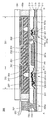
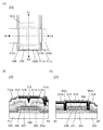
- FIG. 18A shows a top view of a liquid crystal display device 300 that can function as a touch panel
- FIG. 18B shows a cross section between alternate long and short dash lines A-B and between alternate long and short dash lines CD in FIG. The figure is shown.
- the liquid crystal display device 300 includes a display portion 301 and a gate line driver circuit 302.
- the display portion 301 includes a plurality of pixels 303, a plurality of data lines, and a plurality of gate lines, and has a function of displaying an image.
- the display unit 301 is also an input unit. That is, the display unit includes a plurality of detection elements that detect contact or proximity of the detection target to the liquid crystal display device 300, and functions as a touch sensor.
- the gate line driver circuit 302 has a function of outputting a scanning signal to the gate line included in the display portion 301.
- the pixel 303 has a plurality of subpixels.
- FIG. 18A illustrates an example in which the pixel 303 includes three subpixels; however, one embodiment of the present invention is not limited to this.
- FIG. 18A illustrates an example in which the liquid crystal display device 300 includes a gate line driver circuit; however, one embodiment of the present invention is not limited thereto.
- the liquid crystal display device 300 may not include all of the gate line driver circuit, the data line driver circuit, and the sensor driver circuit, or may include one or more of them.
- the IC 268 is mounted on the substrate 211 by a mounting method such as a COG method.
- the IC 268 may have at least one of a data line driver circuit, a gate line driver circuit, and a sensor driver circuit.
- the FPC 269 is electrically connected to the liquid crystal display device 300. Signals are supplied from the outside to the IC 268 and the gate line driver circuit through the FPC 269. Further, a signal can be output from the IC 268 to the outside via the FPC 269.
- An IC may be mounted on the FPC 269.
- the FPC 269 may be mounted with an IC including any one or more of a data line driver circuit, a gate line driver circuit, and a sensor driver circuit.
- the IC can be mounted on the FPC 269 by a mounting method such as a COF method or a TAB (Tape Amount Bonding) method.
- the IC 268 may have a data line driving circuit and a sensor driving circuit.
- the IC 268 may include a data line driver circuit
- the IC mounted on the FPC 269 may include a sensor driver circuit.
- the liquid crystal display device 300 includes a transistor 201a, a transistor 203a, a connection portion 205a, a liquid crystal element 207a, and the like over a substrate 211.
- FIG. 18B shows a cross section of one subpixel as an example of the display portion 301.
- the display unit 301 can perform full-color display by including one pixel including a red sub-pixel, a green sub-pixel, and a blue sub-pixel.
- the color which a subpixel exhibits is not restricted to red, green, and blue.
- a sub-pixel exhibiting a color such as white, yellow, magenta, or cyan may be used.
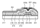
- the transistors 201a and 203a each include a gate electrode 221, an oxide conductive film 227, an insulating film 215, an insulating film 213, an oxide semiconductor film 223, a source electrode 225a, and a drain electrode 225b.
- the gate electrode 221 and the oxide conductive film 227 can each function as a gate.
- the transistor 201a has a structure in which an oxide semiconductor film in which a channel is formed is sandwiched between two gates.
- the gate electrode 221 and the oxide conductive film 227 are electrically connected through the conductive film 226.
- a transistor having a structure in which two gates are electrically connected as described above can increase field-effect mobility and increase on-state current as compared to other transistors. As a result, a circuit capable of high speed operation can be manufactured. Furthermore, the area occupied by the circuit portion can be reduced.
- signal delay in each wiring can be reduced even if the number of wirings is increased when the liquid crystal display device is increased in size or increased in definition. It is possible to suppress.
- a highly reliable transistor can be realized.
- the transistor 203a is configured to give different signals to the two gates as described above. In this manner, by supplying different signals to the two gates and controlling the transistor 203a to operate at different timings, the number of wirings for controlling the transistor can be reduced. As a result, the aperture ratio of the pixel can be improved.
- the transistors 201a and 203a may have the same structure or different structures. That is, the transistor included in the driver circuit portion and the transistor included in the display portion may have the same structure or different structures.
- the transistors 201a and 203a are covered with an insulating film 217 and an insulating film 219.
- the insulating film 217 and the insulating film 219 can also be regarded as components of the transistors 201a and 203a.
- the insulating film 217 preferably has an effect of suppressing diffusion of impurities into a semiconductor included in the transistor.
- the insulating film 217 is preferably formed using a material that does not easily diffuse impurities such as water and hydrogen.
- an insulating film having a planarization function is preferably selected in order to reduce surface unevenness due to the transistor.
- the transistors 201a and 203a have a structure in which an oxide semiconductor film 223 is used as a semiconductor layer and an oxide conductive film 227 is used as a gate. At this time, the oxide semiconductor film 223 and the oxide conductive film 227 are preferably formed using an oxide semiconductor.
- An oxide semiconductor can be suitably used as a material for a semiconductor film and a conductive film because its resistivity can be easily controlled in a manufacturing process of a liquid crystal display device.
- an oxide semiconductor having the same metal element is used for two or more layers included in a liquid crystal display device, so that a manufacturing apparatus (for example, a film formation apparatus or a processing apparatus) is shared by two or more processes. Therefore, the manufacturing cost can be suppressed.
- an oxide semiconductor is a material that transmits visible light, it can be suitably used for an element that transmits visible light. Therefore, even when used as a wiring, a signal can be transmitted without reducing the aperture ratio.
- the oxide semiconductor film 223 and the oxide conductive film 227 are formed using the same metal element, manufacturing cost can be reduced. For example, manufacturing costs can be reduced by using metal oxide targets having the same metal composition. In addition, when a metal oxide target having the same metal composition is used, an etching gas or an etching solution for processing the oxide semiconductor film can be used in common. Note that the oxide semiconductor film 223 and the oxide conductive film 227 may have different compositions even though they have the same metal element. For example, during the manufacturing process of a liquid crystal display device, a metal element in a film may be detached to have a different metal composition.
- the transistors 201a and 203a preferably include the oxide semiconductor film 223 which is highly purified and suppresses formation of oxygen vacancies.
- the current value (off-current value) in the off state of the transistor can be reduced. Therefore, the holding time of an electric signal such as an image signal can be increased, and the writing interval can be set longer in the power-on state. Therefore, since the frequency of the refresh operation can be reduced, there is an effect of suppressing power consumption.
- the transistors 201a and 203a can be driven at high speed because relatively high field-effect mobility can be obtained.
- the transistor in the display portion and the transistor in the driver circuit portion can be formed over the same substrate. That is, it is not necessary to use a separate semiconductor device formed of a silicon wafer or the like as the drive circuit, so that the number of parts of the liquid crystal display device can be reduced.
- a high-quality image can be provided by using a transistor that can be driven at high speed.
- the liquid crystal display device 300 can function as a transmissive liquid crystal display device. Further, by using a conductive material that reflects visible light for the conductive film 251 and a conductive material that transmits visible light for the conductive film 252, the liquid crystal display device 300 functions as a reflective liquid crystal display device. be able to.
- a material containing one kind selected from indium (In), zinc (Zn), and tin (Sn) may be used.
- indium oxide, indium tin oxide (ITO: Indium Tin Oxide) indium zinc oxide, indium oxide containing tungsten oxide, indium zinc oxide containing tungsten oxide, indium oxide containing titanium oxide, Examples thereof include indium tin oxide containing titanium oxide, indium tin oxide added with silicon oxide, zinc oxide, and zinc oxide added with gallium.
- a film containing graphene can also be used. The film containing graphene can be formed, for example, by reducing a film containing graphene oxide formed in a film shape.
- the conductive film 252 is preferably an oxide conductive film.
- the oxide conductive film preferably includes one or more metal elements contained in the oxide semiconductor film 223.
- the conductive film 251 preferably contains indium and is an In-M-Zn oxide (M is Al, Ti, Ga, Y, Zr, La, Ce, Nd, Sn, or Hf) film. preferable.
- the conductive film 252 preferably contains indium, and more preferably an In-M-Zn oxide film.
- At least one of the conductive film 251 and the conductive film 252 may be formed using an oxide semiconductor.
- an oxide semiconductor including the same metal element is used for two or more layers included in a liquid crystal display device, so that a manufacturing apparatus (for example, a film formation apparatus or a processing apparatus) can have two or more steps. Therefore, the manufacturing cost can be reduced.
- the conductivity of the oxide semiconductor can be increased by hydrogen supplied from the insulating film 253.
- Examples of the conductive material that reflects visible light include aluminum, silver, and alloys containing these metal materials.
- the conductive film 251 functioning as a pixel electrode is electrically connected to the source or drain of the transistor 203a.
- an example in which the conductive film 251 is electrically connected to the drain electrode 225b is shown.
- the conductive film 252 has a comb-like upper surface shape (also referred to as a planar shape) or an upper surface shape provided with a slit.
- An insulating film 253 is provided between the conductive films 251 and 252.
- the conductive film 251 has a portion overlapping with the conductive film 252 with the insulating film 253 provided therebetween.
- a portion where the conductive film 252 is not provided over the conductive film 251 is included.
- connection unit 205a is electrically connected to an external input terminal that transmits an external signal (such as a video signal, a clock signal, a start signal, or a reset signal) or a potential to the gate line driver circuit 302.
- an external signal such as a video signal, a clock signal, a start signal, or a reset signal
- FPC 269 is provided as an external input terminal.
- the connection portion 205 a includes a conductive film 231 over the insulating film 213, a conductive film 233 over the conductive film 231, and a conductive film 235 over the conductive film 233.
- the conductive film 231 is electrically connected to the conductive film 235 through the conductive film 233.
- the conductive film 235 is electrically connected to the FPC 269 through the connection body 267.
- the conductive film 231 can be formed using the same material and the same process as the source electrode 225a and the drain electrode 225b included in the transistors 201a and 203a.
- the conductive film 233 can be formed using the same material and the same step as the conductive film 251 included in the liquid crystal element 207a.
- the conductive film 235 can be formed using the same material and the same step as the conductive film 252 included in the liquid crystal element 207a. In this manner, it is preferable that the conductive film included in the connection portion 205a be formed using the same material and the same process as the electrodes and wirings used for the display portion and the driver circuit portion because an increase in the number of steps can be prevented.
- the substrate 261 is provided with a coloring film 241, a light shielding film 243, and an insulating film 245.
- FIG. 18B illustrates an example in which the thickness of the substrate 261 is thinner than the thickness of the substrate 211; however, one embodiment of the present invention is not limited thereto.
- One of the substrate 261 and the substrate 211 may be thinner than the other, or the same thickness. It is preferable to thin the substrate on the display surface side (side closer to the detection target) because the detection sensitivity of the detection element can be increased.
- the colored film 241 has a portion overlapping with the liquid crystal element 207a.
- the light-blocking film 243 includes a portion overlapping with at least one of the transistors 201a and 203a.
- the insulating film 245 preferably has a function as an overcoat that prevents impurities contained in the coloring film 241, the light-shielding film 243, and the like from diffusing into the liquid crystal 249.
- the insulating film 245 is not necessarily provided if not necessary.
- the liquid crystal display device 300 includes a spacer 247.
- the spacer 247 has a function of preventing the distance between the substrate 211 and the substrate 261 from approaching a certain distance.
- FIG. 18B illustrates an example in which the spacer 247 is provided over the insulating film 253 and the conductive film 252, but one embodiment of the present invention is not limited thereto.
- the spacer 247 may be provided on the substrate 211 side or may be provided on the substrate 261 side.
- the spacer 247 may be formed over the insulating film 245.
- 18B illustrates an example in which the spacer 247 is in contact with the insulating film 253 and the insulating film 245; however, the spacer 247 may not be in contact with a structure provided on either the substrate 211 side or the substrate 261 side. .
- a granular spacer may be used as the spacer 247.
- a material such as silica can be used, but an elastic material such as resin or rubber is preferably used. At this time, the granular spacer may be crushed in the vertical direction.
- the substrate 211 and the substrate 261 are bonded together with an adhesive layer 265.
- a liquid crystal 249 is sealed in a region surrounded by the substrate 211, the substrate 261, and the adhesive layer 265.
- the liquid crystal display device 300 When the liquid crystal display device 300 functions as a transmissive liquid crystal display device, two polarizing plates are arranged so as to sandwich the display portion. Light from a backlight disposed outside the polarizing plate is incident through the polarizing plate. At this time, the alignment of the liquid crystal 249 can be controlled by the voltage applied between the conductive films 251 and 252, and the optical modulation of light can be controlled. That is, the intensity of light emitted through the polarizing plate can be controlled. In addition, since the incident light is absorbed by the colored film 241 in a region other than the specific wavelength region, the emitted light is, for example, light exhibiting red, blue, or green.
- liquid crystal element 207a liquid crystal elements to which various modes are applied can be used without being limited thereto.
- VA Vertical Alignment
- TN Transmission Nematic
- IPS In-Plane-Switching
- ASM Analy Symmetrical Aligned Micro-cell
- OCB Optical BLC
- AFLC Antiferroelectric Liquid Crystal
- a normally black liquid crystal display device such as a transmissive liquid crystal display device employing a vertical alignment (VA) mode may be applied to the liquid crystal display device 300.
- VA vertical alignment
- an MVA (Multi-Domain Vertical Alignment) mode, a PVA (Patterned Vertical Alignment) mode, an ASV mode, or the like can be used as the vertical alignment mode.
- the liquid crystal element is an element that controls transmission or non-transmission of light by an optical modulation action of liquid crystal.
- the optical modulation action of the liquid crystal is controlled by an electric field applied to the liquid crystal (including a horizontal electric field, a vertical electric field, or an oblique electric field).
- a thermotropic liquid crystal a low molecular liquid crystal, a polymer liquid crystal, a polymer dispersed liquid crystal (PDLC), a ferroelectric liquid crystal, an antiferroelectric liquid crystal, or the like is used.
- PDLC polymer dispersed liquid crystal
- ferroelectric liquid crystal an antiferroelectric liquid crystal, or the like
- These liquid crystal materials exhibit a cholesteric phase, a smectic phase, a cubic phase, a chiral nematic phase, an isotropic phase, and the like depending on conditions.
- liquid crystal material either a positive type liquid crystal or a negative type liquid crystal may be used, and an optimal liquid crystal material may be used according to the mode and design to be applied.
- a liquid crystal exhibiting a blue phase without using an alignment film may be used.
- the blue phase is one of the liquid crystal phases.
- the temperature of the cholesteric liquid crystal is increased, the blue phase appears immediately before the transition from the cholesteric phase to the isotropic phase. Since the blue phase appears only in a narrow temperature range, a liquid crystal composition in which 5% by weight or more of a chiral agent is mixed is used for the liquid crystal 249 in order to improve the temperature range.
- a liquid crystal composition containing a liquid crystal exhibiting a blue phase and a chiral agent has a short response speed and is optically isotropic.
- a liquid crystal composition including a liquid crystal exhibiting a blue phase and a chiral agent does not require alignment treatment and has a small viewing angle dependency. Further, since it is not necessary to provide an alignment film, a rubbing process is not required, so that electrostatic breakdown caused by the rubbing process can be prevented, and defects or breakage of the liquid crystal display device during the manufacturing process can be reduced. .
- a substrate that is directly touched by a detection object such as a finger or a stylus may be provided above the substrate 261.
- a polarizing plate or a circular polarizing plate is preferably provided between the substrate 261 and the substrate.
- a protective layer ceramic coating or the like
- an inorganic insulating material such as silicon oxide, aluminum oxide, yttrium oxide, and yttria-stabilized zirconia (YSZ) can be used.
- tempered glass may be used for the substrate. As the tempered glass, it is possible to use glass that has been subjected to physical or chemical treatment by an ion exchange method, an air-cooling tempering method, or the like and to which a compressive stress has been applied to the surface.
- FIG. 19A shows a cross-sectional view of two adjacent pixels.
- the two subpixels illustrated in FIG. 19A are subpixels included in different pixels.
- the proximity or contact of the detection target is detected using a capacitance formed between the conductive film 252 included in the left subpixel and the conductive film 252 included in the right subpixel. can do. That is, in the liquid crystal display device of one embodiment of the present invention, the conductive film 252 serves as both the common electrode of the liquid crystal element and the electrode of the detection element.
- the electrode included in the liquid crystal element also serves as the electrode included in the detection element, the manufacturing process can be simplified and the manufacturing cost can be reduced.
- the liquid crystal display device can be reduced in thickness and weight.
- the capacitance between the sensing element electrode and the signal line is too large, the time constant of the sensing element electrode may increase. Therefore, it is preferable to provide an insulating film having a planarization function between the transistor and the electrode of the detection element to reduce the capacitance between the electrode of the detection element and the signal line.
- the insulating film 219 is provided as the insulating film having a planarization function.
- the time constant of the electrodes of the sensing element is greater than 0 seconds and 1 ⁇ 10 ⁇ 4 seconds or less, preferably greater than 0 seconds and 5 ⁇ 10 ⁇ 5 seconds or less, more preferably greater than 0 seconds and 5 ⁇ 10 ⁇ 6 seconds. In the following, it is more preferably greater than 0 seconds and 5 ⁇ 10 ⁇ 7 seconds or less, and more preferably greater than 0 seconds and 2 ⁇ 10 ⁇ 7 seconds or less.
- the time constant is set to 1 ⁇ 10 ⁇ 6 seconds or less, high detection sensitivity can be realized while suppressing the influence of noise.
- FIG. 19B is different from Configuration Example 1 shown in FIGS. 18B and 19A in that a conductive film 255 is provided over the insulating film 253.
- the conductive film 252 is electrically connected to the conductive film 255 functioning as an auxiliary wiring.
- the resistance of the electrode of the detection element can be reduced.
- the time constant of the electrode of the sensing element can be reduced. The smaller the time constant of the electrode of the sensing element, the higher the detection sensitivity, and the higher the detection accuracy.
- FIG. 20 is a cross-sectional view taken along the alternate long and short dash line A-B and between the alternate long and short dash line CD in FIG. 18A, which is different from FIG.
- the colored film 241 is not limited to the structure formed on the counter substrate (substrate 261) side. As shown in FIG. 20, it may be formed on a substrate 211 on which a transistor or the like is formed. Accordingly, it is possible to suppress a decrease in yield and a decrease in display quality due to a decrease in alignment accuracy between the substrate 211 and the substrate 261 accompanying an increase in display definition of the liquid crystal display device.
- FIG. 21 is a cross-sectional view of a liquid crystal display device different from the above-described configuration examples.
- the liquid crystal display device of one embodiment of the present invention is not limited to a touch panel having a structure (full-in-cell type) in which an electrode or the like that forms a detection element is provided only on a substrate that supports a display element.
- an electrode that forms a detection element may be provided on the counter substrate side.
- FIG. 21 shows an example in which a conductive film 254 is formed on the surface of the substrate 261 opposite to the surface on which the colored film 241 and the like are formed.
- An FPC 259 is electrically connected to the conductive film 254 through a connection body 257.
- proximity or contact of a detection target can be detected using a capacitor formed between the conductive film 252 and the conductive film 254. That is, in the liquid crystal display device of one embodiment of the present invention, the conductive film 252 serves as both a common electrode of the liquid crystal element and one electrode of the detection element. As described above, the common electrode of the liquid crystal element may also serve as one electrode of the visual inspection element, or may serve as the pair of electrodes of the detection element.
- ⁇ Board There is no particular limitation on the material of the substrate included in the liquid crystal display device 300, but it is necessary to have at least heat resistance to withstand heat treatment performed later.
- a glass substrate, a ceramic substrate, a quartz substrate, a sapphire substrate, or the like may be used. It is also possible to apply a single crystal semiconductor substrate made of silicon or silicon carbide, a polycrystalline semiconductor substrate, a compound semiconductor substrate such as silicon germanium, an SOI substrate, etc., and a semiconductor element provided on these substrates May be used as the substrate 102.
- the sixth generation (1500 mm ⁇ 1850 mm), the seventh generation (1870 mm ⁇ 2200 mm), the eighth generation (2200 mm ⁇ 2400 mm), the ninth generation (2400 mm ⁇ 2800 mm), the tenth generation.
- a large area substrate such as a generation (2950 mm ⁇ 3400 mm)
- a large display device can be manufactured.
- a flexible substrate may be used as the substrate 211, and a transistor, a capacitor, or the like may be formed directly over the flexible substrate.
- the liquid crystal display device can be reduced in weight and thickness. Further, a flexible liquid crystal display device can be realized by using a flexible substrate.
- a transistor can be formed using various substrates as the substrates 211 and 261.
- substrate is not limited to a specific thing.
- the substrate include a plastic substrate, a metal substrate, a stainless steel substrate, a substrate having a stainless steel foil, a tungsten substrate, a substrate having a tungsten foil, a flexible substrate, a bonded film, and a fibrous material. Or a base film.
- the glass substrate include barium borosilicate glass, aluminoborosilicate glass, and soda lime glass.
- a transistor may be formed using a certain substrate, and then the transistor may be transferred to another substrate, and the transistor may be disposed on another substrate.
- the substrate on which the transistor is transferred in addition to the substrate on which the transistor can be formed, a paper substrate, a cellophane substrate, a stone substrate, a wood substrate, a cloth substrate (natural fiber (silk, cotton, hemp), There are synthetic fibers (nylon, polyurethane, polyester) or recycled fibers (including acetate, cupra, rayon, recycled polyester), leather substrates, rubber substrates, and the like. By using these substrates, it is possible to form a transistor with good characteristics, a transistor with low power consumption, manufacture a device that is not easily broken, impart heat resistance, reduce weight, or reduce thickness.
- ⁇ Transistor ⁇ There is no particular limitation on the structure of the transistor included in the liquid crystal display device of one embodiment of the present invention. For example, a planar transistor, a staggered transistor, or an inverted staggered transistor may be used. Further, a top-gate or bottom-gate transistor structure may be employed. Alternatively, gate electrodes may be provided above and below the channel.
- a semiconductor material used for the transistor is not particularly limited, and examples thereof include an oxide semiconductor, silicon, and germanium.
- crystallinity of a semiconductor material used for the transistor there is no particular limitation on the crystallinity of a semiconductor material used for the transistor, and any of an amorphous semiconductor and a semiconductor having crystallinity (a microcrystalline semiconductor, a polycrystalline semiconductor, a single crystal semiconductor, or a semiconductor partially including a crystal region) is used. May be used. It is preferable to use a crystalline semiconductor because deterioration of transistor characteristics can be suppressed.
- a semiconductor material used for the transistor for example, an element belonging to Group 14, a compound semiconductor, or an oxide semiconductor can be used for the semiconductor layer.
- a semiconductor containing silicon, a semiconductor containing gallium arsenide, an oxide semiconductor containing indium, or the like can be used.
- an oxide semiconductor is preferably used for a semiconductor in which a channel of a transistor is formed.
- an oxide semiconductor having a larger band gap than silicon is preferably used. It is preferable to use a semiconductor material with a wider band gap and lower carrier density than silicon because current in an off state of the transistor can be reduced.
- the oxide semiconductor preferably contains at least indium (In) or zinc (Zn). More preferably, an oxide represented by an In-M-Zn oxide (M is a metal such as Al, Ti, Ga, Ge, Y, Zr, Sn, La, Ce, Hf, or Nd) is included.
- M is a metal such as Al, Ti, Ga, Ge, Y, Zr, Sn, La, Ce, Hf, or Nd
- Such an oxide semiconductor does not have a crystal grain boundary, cracks in the oxide semiconductor film due to stress when the display panel is bent is suppressed. Therefore, such an oxide semiconductor can be favorably used for a liquid crystal display device that is flexible and used by being bent.
- the charge accumulated in the capacitor through the transistor can be held for a long time.
- the driving circuit can be stopped while maintaining the gradation of an image displayed in each display region. As a result, a display device with extremely reduced power consumption can be realized.
- a transistor using a polysilicon film has high field effect mobility
- various functional circuits such as a shift register circuit, a level shifter circuit, a buffer circuit, and a sampling circuit can be formed.
- the oxide semiconductor film 223 includes an In-M-Zn oxide containing at least indium (In), zinc (Zn), and M (metal such as Al, Ti, Ga, Y, Zr, La, Ce, Sn, or Hf). It is preferable that the film
- the stabilizer examples include gallium (Ga), tin (Sn), hafnium (Hf), aluminum (Al), zirconium (Zr), and the like, including the metals described in M above.
- Other stabilizers include lanthanoids such as lanthanum (La), cerium (Ce), praseodymium (Pr), neodymium (Nd), samarium (Sm), europium (Eu), gadolinium (Gd), terbium (Tb). ), Dysprosium (Dy), holmium (Ho), erbium (Er), thulium (Tm), ytterbium (Yb), lutetium (Lu), and the like.
- oxide semiconductor included in the oxide semiconductor film 223 examples include an In—Ga—Zn-based oxide, an In—Al—Zn-based oxide, an In—Sn—Zn-based oxide, and an In—Hf—Zn-based oxide.
- the In—Ga—Zn-based oxide means an oxide containing In, Ga, and Zn as main components, and the ratio of In, Ga, and Zn is not limited. Moreover, metal elements other than In, Ga, and Zn may be contained.
- the oxide semiconductor film 223 is an In-M-Zn oxide
- In is preferably higher than 25 atomic%
- M is less than 75 atomic%
- the oxide semiconductor film 223 has an energy gap of 2 eV or more, preferably 2.5 eV or more, more preferably 3 eV or more. In this manner, off-state current of a transistor can be reduced by using an oxide semiconductor with a wide energy gap.
- the thickness of the oxide semiconductor film 223 is 3 nm to 200 nm, preferably 3 nm to 100 nm, more preferably 3 nm to 50 nm.
- the oxide semiconductor film 223 is an In-M-Zn oxide (M is Al, Ga, Y, Zr, La, Ce, or Nd)
- a sputtering target used to form an In-M-Zn oxide It is preferable that the atomic ratio of the metal elements satisfies In ⁇ M and Zn ⁇ M.
- the atomic ratio of the oxide semiconductor film 223 to be formed includes a variation of plus or minus 40% of the atomic ratio of the metal element contained in the sputtering target as an error.
- the oxide semiconductor film 2223 an oxide semiconductor film with low carrier density is used.
- the oxide semiconductor film 223 has a carrier density of 1 ⁇ 10 17 / cm 3 or less, preferably 1 ⁇ 10 15 / cm 3 or less, more preferably 1 ⁇ 10 13 / cm 3 or less, more preferably 1 ⁇ 10.
- An oxide semiconductor film of 11 / cm 3 or less is used.
- a transistor having an appropriate composition may be used depending on required semiconductor characteristics and electrical characteristics (such as field-effect mobility and threshold voltage) of a transistor.
- the carrier density, impurity concentration, defect density, atomic ratio of metal element to oxygen, interatomic distance, density, and the like of the oxide semiconductor film 223 are appropriate. It is preferable.
- the concentration of silicon or carbon (concentration obtained by secondary ion mass spectrometry) in the oxide semiconductor film 223 is 2 ⁇ 10 18 atoms / cm 3 or less, preferably 2 ⁇ 10 17 atoms / cm 3 or less.
- the concentration of alkali metal or alkaline earth metal obtained by secondary ion mass spectrometry is 1 ⁇ 10 18 atoms / cm 3 or less, preferably 2 ⁇ 10 16 atoms / cm 3 or less.
- the nitrogen concentration obtained by secondary ion mass spectrometry is preferably 5 ⁇ 10 18 atoms / cm 3 or less. .
- the oxide semiconductor film 223 may have a non-single crystal structure, for example.
- the non-single crystal structure includes, for example, a CAAC-OS (C Axis Aligned-Crystalline Oxide Semiconductor) described later, a polycrystalline structure, a microcrystalline structure described later, or an amorphous structure.
- CAAC-OS C Axis Aligned-Crystalline Oxide Semiconductor
- the amorphous structure has the highest density of defect states
- the CAAC-OS has the lowest density of defect states.
- the oxide semiconductor film 223 may have an amorphous structure, for example.
- An oxide semiconductor film having an amorphous structure has, for example, disordered atomic arrangement and no crystal component.
- an amorphous oxide film has, for example, a completely amorphous structure and does not have a crystal part.
- the oxide semiconductor film 223 may be a mixed film including two or more of an amorphous structure region, a microcrystalline structure region, a polycrystalline structure region, a CAAC-OS region, and a single crystal structure.
- the mixed film may include two or more of an amorphous structure region, a microcrystalline structure region, a polycrystalline structure region, a CAAC-OS region, and a single crystal structure region.
- the mixed film has a stacked structure of two or more of an amorphous structure region, a microcrystalline structure region, a polycrystalline structure region, a CAAC-OS region, and a single crystal structure region. May have.
- silicon is preferably used for a semiconductor in which a transistor channel is formed.
- amorphous silicon may be used as silicon, it is particularly preferable to use silicon having crystallinity.
- microcrystalline silicon, polycrystalline silicon, single crystal silicon, or the like is preferably used.
- polycrystalline silicon can be formed at a lower temperature than single crystal silicon, and has higher field effect mobility and higher reliability than amorphous silicon.
- the aperture ratio of the pixel can be improved.
- the gate driver circuit and the source driver circuit can be formed over the same substrate as the pixel, and the number of components included in the electronic device can be reduced.
- An oxide semiconductor is a semiconductor material whose resistance can be controlled by oxygen vacancies in the film and / or the concentration of impurities such as hydrogen and water in the film. Therefore, the resistivity of the oxide conductive film can be controlled by selecting a treatment for increasing the oxygen deficiency or / and impurity concentration or a treatment for reducing the oxygen deficiency or / and impurity concentration in the oxide semiconductor film. it can.
- an oxide conductive film formed using an oxide semiconductor film as described above is an oxide semiconductor film with high carrier density and low resistance, an oxide semiconductor film with conductivity, or an oxide with high conductivity. It can also be called a semiconductor film.
- oxide semiconductor film is formed in contact with the insulating film 217 containing hydrogen, and hydrogen is diffused from the insulating film 217 containing hydrogen into the oxide semiconductor film, whereby the oxide semiconductor has high carrier density and low resistance. It can be a membrane.
- an insulating film 215 is provided over the oxide semiconductor film 223 so that the oxide semiconductor film 223 is not exposed to the plasma treatment.
- the insulating film 215 is provided so that the oxide semiconductor film 223 is not in contact with the insulating film 217 containing hydrogen.
- oxygen can be supplied to the oxide semiconductor film 223.
- the oxide semiconductor film 223 to which oxygen is supplied becomes a high-resistance oxide semiconductor with reduced oxygen vacancies in the film or at the interface.
- the insulating film from which oxygen can be released for example, a silicon oxide film or a silicon oxynitride film can be used.
- hydrogen, boron, phosphorus, or nitrogen is implanted into the oxide semiconductor film by an ion implantation method, an ion doping method, a plasma immersion ion implantation method, or the like. May be.
- the plasma treatment performed on the oxide conductive film 227 typically includes one kind selected from a rare gas (He, Ne, Ar, Kr, and Xe), phosphorus, boron, hydrogen, and nitrogen.
- Plasma treatment using a gas can be mentioned. More specifically, plasma treatment in an Ar atmosphere, plasma treatment in a mixed gas atmosphere of Ar and hydrogen, plasma treatment in an ammonia atmosphere, plasma treatment in a mixed gas atmosphere of Ar and ammonia, or nitrogen For example, plasma treatment in an atmosphere.
- oxygen vacancies are formed in the oxide conductive film 227 in the lattice from which oxygen is released (or the portion from which oxygen is released).
- the oxygen deficiency may be a factor that generates carriers.
- hydrogen when hydrogen is supplied from the insulating film in contact with the oxide conductive film 227, more specifically, below or above the oxide conductive film 227, when hydrogen enters the oxygen vacancies, electrons serving as carriers are changed. May be generated. Therefore, the oxide conductive film 227 in which oxygen vacancies are increased by plasma treatment has a higher carrier density than the oxide semiconductor film 223.
- the oxide semiconductor film 223 in which oxygen vacancies are reduced and the hydrogen concentration is reduced can be said to be a highly purified intrinsic or substantially highly purified intrinsic oxide semiconductor film.
- substantially intrinsic means that the carrier density of the oxide semiconductor is less than 1 ⁇ 10 17 / cm 3 , preferably less than 1 ⁇ 10 15 / cm 3 , and more preferably 1 ⁇ 10 10. It indicates less than 13 / cm 3 .
- a low impurity concentration and a low density of defect states (small number of oxygen vacancies) is called high-purity intrinsic or substantially high-purity intrinsic.
- An oxide semiconductor that is highly purified intrinsic or substantially highly purified intrinsic has few carrier generation sources, and thus can have a low carrier density.
- a transistor in which a channel region is formed in the oxide semiconductor film easily has electrical characteristics (also referred to as normally-off characteristics) in which the threshold voltage is positive.
- the oxide semiconductor film 223 which is highly purified intrinsic or substantially highly purified intrinsic has a low defect level density; therefore, the trap level density can be reduced.
- the oxide semiconductor film 223 which is highly purified intrinsic or substantially highly purified intrinsic has an extremely small off-state current, a channel width of 1 ⁇ 10 6 ⁇ m, and a channel length L of 10 ⁇ m.
- the off-state current can be less than the measurement limit of the semiconductor parameter analyzer, that is, 1 ⁇ 10 ⁇ 13 A or less. Therefore, a transistor in which a channel region is formed in the oxide semiconductor film 223 has little variation in electric characteristics and has high reliability.
- an insulating film containing hydrogen in other words, an insulating film capable of releasing hydrogen, typically a silicon nitride film, is used to supply hydrogen to the oxide conductive film 227. it can.
- the insulating film capable of releasing hydrogen preferably has a hydrogen concentration in the film of 1 ⁇ 10 22 atoms / cm 3 or more. By forming such an insulating film in contact with the oxide conductive film 227, the oxide conductive film 227 can effectively contain hydrogen.
- the resistance of the oxide semiconductor film (or oxide conductive film) can be arbitrarily set by changing the structure of the insulating film in contact with the oxide semiconductor film (or oxide conductive film) in combination with the plasma treatment described above. Can be adjusted.
- Hydrogen contained in the oxide conductive film 227 reacts with oxygen bonded to metal atoms to become water, and forms oxygen vacancies in a lattice from which oxygen is released (or a portion from which oxygen is released). When hydrogen enters the oxygen vacancies, electrons serving as carriers may be generated. In some cases, a part of hydrogen is bonded to oxygen bonded to a metal atom, so that an electron serving as a carrier is generated. Therefore, the oxide conductive film 227 containing hydrogen has a higher carrier density than the oxide semiconductor film 223.
- the oxide semiconductor film 223 in which the channel region of the transistor is formed preferably has as much hydrogen as possible.
- a hydrogen concentration obtained by secondary ion mass spectrometry is 2 ⁇ 10 20 atoms / cm 3 or less, preferably 5 ⁇ 10 19 atoms. / Cm 3 or less, more preferably 1 ⁇ 10 19 atoms / cm 3 or less, preferably less than 5 ⁇ 10 18 atoms / cm 3 , preferably 1 ⁇ 10 18 atoms / cm 3 or less, more preferably 5 ⁇ 10 17 atoms / cm 3. 3 or less, more preferably 1 ⁇ 10 16 atoms / cm 3 or less.
- the oxide conductive film 227 functioning as a gate has a higher hydrogen concentration and / or oxygen deficiency than the oxide semiconductor film 223 and has a reduced resistance.
- the oxide semiconductor film 223 and the oxide conductive film 227 typically include an In—Ga oxide, an In—Zn oxide, and an In—M—Zn oxide (M represents Mg, Al, Ti, Ga, and Y). , Zr, La, Ce, Nd, or Hf). Note that the oxide semiconductor film 223 and the oxide conductive film 227 have a light-transmitting property.
- the oxide semiconductor film 223 is an In—M—Zn oxide
- In is 25 atomic% or more
- M is less than 75 atomic%
- In is 34 atomic% or more
- M Is less than 66 atomic%.
- the oxide semiconductor film 223 has an energy gap of 2 eV or more, 2.5 eV or more, or 3 eV or more.
- the thickness of the oxide semiconductor film 223 can be 3 nm to 200 nm, 3 nm to 100 nm, or 3 nm to 60 nm.
- the oxide semiconductor film 223 is an In-M-Zn oxide
- the atomic ratio of metal elements of a sputtering target used for forming the In-M-Zn oxide satisfies In ⁇ M and Zn ⁇ M. It is preferable.
- the atomic ratio of the oxide semiconductor film 223 to be formed includes a variation of plus or minus 40% of the atomic ratio of the metal element contained in the sputtering target as an error.
- a material that can be used for the oxide conductive film 227 and a formation method of the oxide conductive film 227 can be applied to the conductive film 251 and the conductive film 252, respectively.
- an organic insulating material or an inorganic insulating material can be used as an insulating material that can be used for each insulating film, overcoat, spacer, and the like included in the liquid crystal display device.
- the resin include acrylic resin, epoxy resin, polyimide resin, polyamide resin, polyimide amide resin, siloxane resin, benzocyclobutene resin, and phenol resin.
- inorganic insulating films include silicon oxide films, silicon oxynitride films, silicon nitride oxide films, silicon nitride films, aluminum oxide films, hafnium oxide films, yttrium oxide films, zirconium oxide films, gallium oxide films, tantalum oxide films, magnesium oxide Examples thereof include a film, a lanthanum oxide film, a cerium oxide film, and a neodymium oxide film.
- conductive films such as various wirings and electrodes of a liquid crystal display device include aluminum, titanium, chromium, nickel, copper, yttrium, zirconium, molybdenum, silver, tantalum, and tungsten.
- a metal or an alloy containing the same as a main component can be used as a single layer structure or a stacked structure.
- a two-layer structure in which a titanium film is laminated on an aluminum film a two-layer structure in which a titanium film is laminated on a tungsten film, a two-layer structure in which a copper film is laminated on a molybdenum film, or an alloy film containing molybdenum and tungsten
- Two-layer structure in which a copper film is laminated a two-layer structure in which a copper film is laminated on a copper-magnesium-aluminum alloy film, a titanium film or a titanium nitride film, and an aluminum film or copper layered on the titanium film or titanium nitride film Laminating a film, and further forming a three-layer structure for forming a titanium film or a titanium nitride film thereon, a molybdenum film or a molybdenum nitride film, and an aluminum film or a copper film stacked on the molybdenum film or the molybdenum nit
- the first and third layers include titanium, titanium nitride, molybdenum, tungsten, an alloy containing molybdenum and tungsten, an alloy containing molybdenum and zirconium, or A film made of molybdenum nitride is formed, and a film made of a low resistance material such as copper, aluminum, gold or silver, or an alloy of copper and manganese is preferably formed in the second layer.
- indium tin oxide indium oxide containing tungsten oxide, indium zinc oxide containing tungsten oxide, indium oxide containing titanium oxide, indium tin oxide containing titanium oxide, indium zinc oxide, silicon oxide
- a light-transmitting conductive material such as indium tin oxide may be used.
- the conductive film may be formed using the above-described method for controlling the resistivity of an oxide semiconductor.
- a curable resin such as a thermosetting resin, a photocurable resin, or a two-component mixed curable resin can be used.
- an acrylic resin, polyurethane, epoxy resin, or a resin having a siloxane bond can be used.
- connection body for example, an anisotropic conductive film (ACF), an anisotropic conductive paste (ACP), or the like can be used.
- ACF anisotropic conductive film
- ACP anisotropic conductive paste
- the colored film is a colored layer that transmits light in a specific wavelength band.
- materials that can be used for the colored film include metal materials, resin materials, resin materials containing pigments or dyes, and the like.
- the light shielding film is provided between the adjacent colored films.
- a black matrix may be formed using a resin material including a metal material, a pigment, or a dye.
- the light-shielding film is preferably provided in a region other than the display portion such as a driver circuit portion because unintended light leakage due to guided light or the like can be suppressed.
- FIG. 22 is a block diagram of the touch panel module 6500.
- the touch panel module 6500 includes a touch panel 6510 and an IC 6520.
- the liquid crystal display device of one embodiment of the present invention can be applied to the touch panel 6510.
- the touch panel 6510 includes a display portion 6511, an input portion 6512, and a gate line driving circuit 6513.
- the display portion 6511 includes a plurality of pixels, a plurality of data lines, and a plurality of gate lines, and has a function of displaying an image.
- the input unit 6512 includes a plurality of detection elements that detect contact or proximity of the detection target to the touch panel 6510, and functions as a touch sensor.
- the gate line driver circuit 6513 has a function of outputting a scanning signal to the gate line included in the display portion 6511.
- the display unit 6511 and the input unit 6512 are separately shown as the configuration of the touch panel 6510, but both the function of displaying an image and the function of a touch sensor are provided.
- a so-called in-cell type touch panel is preferable.
- the liquid crystal display device of one embodiment of the present invention is an in-cell touch panel, which is preferable.
- the display unit 6511 includes HD (pixel count 1280 ⁇ 720), FHD (pixel count 1920 ⁇ 1080), WQHD (pixel count 2560 ⁇ 1440), WQXGA (pixel count 2560 ⁇ 1600), 4K (pixel count 3840 ⁇ 2160), It is preferable to have an extremely high resolution of 8K (number of pixels: 7680 ⁇ 4320). In particular, a resolution of 4K, 8K, or higher is preferable.
- the pixel density (definition) of the pixels provided in the display portion 6511 is preferably 300 ppi or more, preferably 500 ppi or more, more preferably 800 ppi or more, more preferably 1000 ppi or more, and more preferably 1200 ppi or more. With the display portion 6511 having high resolution and high definition in this way, it is possible to further enhance the sense of presence and depth in personal use such as portable and home use.
- the IC 6520 includes a circuit unit 6501, a data line driver circuit 6502, a sensor driver circuit 6503, and a detection circuit 6504.
- the circuit unit 6501 includes a timing controller 6505, an image processing circuit 6506, and the like.
- the data line driver circuit 6502 has a function of outputting a video signal (also referred to as a video signal) which is an analog signal to a data line included in the display portion 6511.
- a video signal also referred to as a video signal
- the data line driver circuit 6502 can have a structure in which a shift resist circuit and a buffer circuit are combined.
- the touch panel 6510 may include a demultiplexer circuit connected to the data line.
- the sensor drive circuit 6503 has a function of outputting a signal for driving a detection element included in the input unit 6512.
- the sensor driving circuit 6503 for example, a structure in which a shift register circuit and a buffer circuit are combined can be used.
- the detection circuit 6504 has a function of outputting an output signal from a detection element included in the input unit 6512 to the circuit unit 6501.
- the detection circuit 6504 can have a structure including an amplifier circuit and an analog-digital converter (ADC). At this time, the detection circuit 6504 converts the analog signal output from the input unit 6512 into a digital signal and outputs the digital signal to the circuit unit 6501.
- ADC analog-digital converter
- the image processing circuit 6506 included in the circuit unit 6501 has a function of generating and outputting a signal for driving the display unit 6511 of the touch panel 6510, a function of generating and outputting a signal for driving the input unit 6512, and an input unit 6512. A function of analyzing the output signal and outputting it to the CPU 6540.
- the image processing circuit 6506 has a function of generating a video signal in accordance with a command from the CPU 6540.
- the image processing circuit 6506 has a function of performing signal processing on the video signal in accordance with the specification of the display portion 6511, converting the video signal into an analog video signal, and supplying the analog video signal to the data line driver circuit 6502.
- the image processing circuit 6506 has a function of generating a drive signal to be output to the sensor drive circuit 6503 in accordance with a command from the CPU 6540.
- the image processing circuit 6506 has a function of analyzing a signal input from the detection circuit 6504 and outputting it to the CPU 6540 as position information.
- the timing controller 6505 also outputs signals (such as a clock signal and a start pulse signal) output to the gate line driver circuit 6513 and the sensor driver circuit 6503 based on the synchronization signal included in the video signal or the like processed by the image processing circuit 6506. Signal) is generated and output.
- the timing controller 6505 may have a function of generating and outputting a signal that defines the timing at which the detection circuit 6504 outputs a signal.
- the timing controller 6505 preferably outputs a signal synchronized with a signal output to the gate line driver circuit 6513 and a signal output to the sensor driver circuit 6503. In particular, it is preferable to divide the period for rewriting pixel data of the display portion 6511 and the period for sensing by the input portion 6512.
- the touch panel 6510 can be driven by dividing one frame period into a period for rewriting pixel data and a period for sensing. Further, for example, by providing two or more sensing periods in one frame period, the detection sensitivity and the detection accuracy can be increased.
- a configuration having a processor can be used.
- other microprocessors such as a DSP (Digital Signal Processor) and a GPU (Graphics Processing Unit) can be used.
- these microprocessors may be realized by PLD (Programmable Logic Device) such as FPGA (Field Programmable Gate Array) and FPAA (Field Programmable Analog Array).
- PLD Programmable Logic Device
- FPGA Field Programmable Gate Array
- FPAA Field Programmable Analog Array
- Various data processing and program control are performed by interpreting and executing instructions from various programs by the processor.
- the program that can be executed by the processor may be stored in a memory area of the processor, or may be stored in a storage device provided separately.
- channel formation is performed in the display portion 6511 included in the touch panel 6510, the gate line driver circuit 6513, the circuit unit 6501 included in the IC 6520, the data line driver circuit 6502, the sensor driver circuit 6503, the detection circuit 6504, or the CPU 6540 provided outside.
- a transistor in which an oxide semiconductor is used for a region and an extremely low off-state current is realized can be used. Since the transistor has extremely low off-state current, the use of the transistor as a switch for holding charge (data) flowing into the capacitor functioning as a memory element can ensure a data holding period for a long time. it can.
- the image processing circuit 6506 is operated only when necessary, and in other cases, the information of the immediately preceding process is saved in the storage element, Normally-off computing is possible, and the power consumption of the touch panel module 6500 and the electronic device in which the touch panel module 6500 is mounted can be reduced.
- the circuit unit 6501 includes the timing controller 6505 and the image processing circuit 6506 here, the image processing circuit 6506 itself or a circuit having a part of the function of the image processing circuit 6506 may be provided outside. .
- the CPU 6540 may perform a function of the image processing circuit 6506 or a part of the functions.
- the circuit unit 6501 can include a data line driver circuit 6502, a sensor driver circuit 6503, a detection circuit 6504, and a timing controller 6505.
- the circuit unit 6501 may be configured not to be included in the IC 6520.
- the IC 6520 can include a data line driver circuit 6502, a sensor driver circuit 6503, and a detection circuit 6504.
- a circuit unit 6501 can be provided separately and a plurality of ICs 6520 without the circuit unit 6501 can be provided, or an IC having only the IC 6520 and the data line driver circuit 6502. Can also be arranged in combination.
- the function of driving the display portion 6511 of the touch panel 6510 and the function of driving the input portion 6512 are incorporated into one IC, so that the number of ICs mounted on the touch panel module 6500 is reduced. Therefore, the cost can be reduced.
- FIGS. 23A, 23B, and 23C are schematic views of a touch panel module 6500 mounted with an IC6520.
- the touch panel module 6500 includes a substrate 6531, a counter substrate 6532, a plurality of FPCs 6533, IC6520, IC6530, and the like.
- a display portion 6511, an input portion 6512, and a gate line driver circuit 6513 are provided between the substrate 6531 and the counter substrate 6532.
- the IC 6520 and the IC 6530 are mounted on the substrate 6531 by a mounting method such as a COG method.
- the IC 6530 is an IC having only the data line driver circuit 6502 or the data line driver circuit 6502 and the circuit unit 6501 in the above-described IC 6520. Signals are supplied to the IC 6520 and the IC 6530 from the outside via the FPC 6533. Further, a signal can be output from the IC 6520 or the IC 6530 to the outside through the FPC 6533.
- FIG. 23A illustrates an example of a structure in which two gate line driver circuits 6513 are provided so that the display portion 6511 is interposed therebetween.
- a configuration including an IC 6530 in addition to the IC 6520 is shown. Such a configuration can be preferably used when the display portion 6511 has an extremely high resolution.
- FIG. 23B shows an example in which one IC 6520 and one FPC 6533 are mounted. Thus, it is preferable to consolidate functions into one IC 6520 because the number of parts can be reduced.
- FIG. 23B illustrates an example in which the gate line driver circuit 6513 is arranged along the side closer to the FPC 6533 out of the two short sides of the display portion 6511.
- FIG. 23C illustrates an example of a configuration including a PCB (Printed Circuit Board) 6534 on which an image processing circuit 6506 and the like are mounted.
- the IC 6520 and the IC 6530 on the substrate 6531 are electrically connected to the PCB 6534 by the FPC 6533.
- a configuration without the above-described image processing circuit 6506 can be applied to the IC 6520.
- the IC 6520 and the IC 6530 may be mounted on the FPC 6533 instead of the substrate 6531.
- the IC 6520 and the IC 6530 may be mounted on the FPC 6533 by a mounting method such as a COF method or a TAB method.
- the configuration in which the FPC 6533, the IC 6520 (and the IC 6530), and the like are arranged on the short side of the display portion 6511 can be narrowed.
- the structure using the PCB 6534 as shown in FIG. 23C can be preferably used, for example, for a television device, a monitor device, a tablet terminal, a laptop personal computer, or the like.
- Embodiment 3 a method for manufacturing a liquid crystal display device according to one embodiment of the present invention will be described with reference to FIGS.
- a method for manufacturing a transistor is mainly described. Note that the description in Embodiment Mode 2 can be referred to for the material of each layer.
- the gate electrode 221 is formed on the substrate 211. After that, an insulating film 213 including the insulating films 106 and 107 is formed over the substrate 211 and the gate electrode 221 (FIG. 24A).
- a glass substrate is used as the substrate 211, a tungsten film is used as the gate electrode 221, a silicon nitride film capable of releasing hydrogen is used as the insulating film 106, and oxygen is released as the insulating film 107.
- a silicon oxide film that can be used is used.
- the insulating film 106 functions as a blocking film that suppresses permeation of oxygen.
- the insulating film 106 can suppress permeation of oxygen.
- the insulating film 107 in contact with the oxide semiconductor film 223 functioning as a channel region of the transistor is preferably an oxide insulating film, and includes a region containing oxygen in excess of the stoichiometric composition (oxygen-excess region). It is more preferable to have.
- the insulating film 107 is an insulating film capable of releasing oxygen.
- the insulating film 107 may be formed in an oxygen atmosphere.
- oxygen may be introduced into the insulating film 107 after film formation to form an oxygen excess region.
- an ion implantation method, an ion doping method, a plasma immersion ion implantation method, a plasma treatment, or the like can be used.
- hafnium oxide when hafnium oxide is used for one or both of the insulating film 106 and the insulating film 107, the following effects are obtained.
- Hafnium oxide has a higher dielectric constant than silicon oxide or silicon oxynitride. Therefore, compared with the case where silicon oxide is used, the thickness of one or both of the insulating film 106 and the insulating film 107 can be increased, so that the leakage current due to the tunnel current can be reduced. That is, a transistor with a small off-state current can be realized.
- hafnium oxide having a crystal structure has a higher dielectric constant than hafnium oxide having an amorphous structure.
- hafnium oxide having a crystal structure examples include a monoclinic system and a cubic system. Note that one embodiment of the present invention is not limited thereto.
- a silicon nitride film is formed as the insulating film 106 and a silicon oxide film is formed as the insulating film 107.
- the silicon nitride film has a relative dielectric constant higher than that of the silicon oxide film, and has a large film thickness necessary for obtaining a capacitance equivalent to that of the silicon oxide film.
- the gate electrode 221 can be formed by forming a conductive film on the substrate 211, patterning the conductive film so that a desired region remains, and then etching unnecessary regions.
- an oxide semiconductor film 223 is formed at a position overlapping with the gate electrode 221 over the insulating film 213 (FIG. 24B).
- the oxide semiconductor film 223 can be formed by forming an oxide semiconductor film over the insulating film 213, patterning the oxide semiconductor film so that a desired region remains, and then etching an unnecessary region. .
- Heat treatment is preferably performed after the oxide semiconductor film 223 is formed.
- the heat treatment is performed at a temperature of 250 ° C. or higher and 650 ° C. or lower, preferably 300 ° C. or higher and 500 ° C. or lower, more preferably 350 ° C. or higher and 450 ° C. or lower. Just do it.
- the heat treatment may be performed in an atmosphere containing 10 ppm or more of an oxidizing gas in order to supplement oxygen released from the oxide semiconductor film 223 after the heat treatment in an inert gas atmosphere.
- impurities such as hydrogen and water can be removed from at least one of the insulating films 106 and 107 and the oxide semiconductor film 223. Note that the heat treatment may be performed before the oxide semiconductor film 223 is processed into an island shape.
- the oxide semiconductor film 223 is intrinsic or substantially intrinsic. It is effective to do.
- a conductive film is formed over the insulating film 213 and the oxide semiconductor film 223, patterned so that a desired region of the conductive film remains, and then unnecessary regions are etched, whereby the insulating film 213 and the oxide film are oxidized.
- a source electrode 225a and a drain electrode 225b are formed over the physical semiconductor film 223 (FIG. 24C).
- a three-layer structure of a tungsten film, an aluminum film, and a titanium film is used as the source electrode 225a and the drain electrode 225b.
- the surface of the oxide semiconductor film 223 may be cleaned after the source electrode 225a and the drain electrode 225b are formed.
- the cleaning method include cleaning using a chemical solution such as phosphoric acid.
- a chemical solution such as phosphoric acid
- impurities attached to the surface of the oxide semiconductor film 223 for example, elements contained in the source electrode 225a and the drain electrode 225b
- the cleaning is not necessarily performed, and in some cases, the cleaning may not be performed.
- the region exposed from the source electrode 225a and the drain electrode 225b of the oxide semiconductor film 223 may be thinned.
- an insulating film 215 including insulating films 114 and 116 is formed over the insulating film 213, the oxide semiconductor film 223, the source electrode 225a, and the drain electrode 225b. Then, patterning is performed so that a desired region of the insulating film 215 remains, and then an unnecessary region is etched to form an opening 141 (FIG. 24D).
- the insulating film 114 it is preferable to continuously form the insulating film 116 without exposure to the air.
- the insulating film 114 and the insulating film are formed by continuously forming the insulating film 116 by adjusting one or more of the flow rate, pressure, high frequency power, and substrate temperature of the source gas without opening to the atmosphere.
- the concentration of impurities derived from atmospheric components can be reduced at the interface with 116, and oxygen contained in the insulating films 114 and 116 can be moved to the oxide semiconductor film 223, so that oxygen vacancies in the oxide semiconductor film 223 can be reduced.
- the amount can be reduced.
- the insulating film 114 serves as a protective film for the oxide semiconductor film 223. Therefore, the insulating film 116 can be formed using high-frequency power with high power density while reducing damage to the oxide semiconductor film 223.
- a silicon oxynitride film capable of releasing oxygen is used as the insulating films 114 and 116.
- the insulating film 114 in contact with the oxide semiconductor film 223 functioning as a channel region of the transistor is preferably an oxide insulating film, and an insulating film capable of releasing oxygen is used.
- the insulating film capable of releasing oxygen is an insulating film having a region (oxygen-excess region) containing oxygen in excess of the stoichiometric composition.
- the insulating film 114 may be formed in an oxygen atmosphere.
- oxygen may be introduced into the insulating film 114 after film formation to form an oxygen excess region.
- an ion implantation method, an ion doping method, a plasma immersion ion implantation method, a plasma treatment, or the like can be used.
- the amount of released oxygen molecules measured by temperature-programmed desorption gas analysis when the film surface temperature is in the range of 100 ° C. to 700 ° C. or 100 ° C. to 500 ° C.
- TDS analysis temperature-programmed desorption gas analysis
- the insulating film 114 preferably has a small amount of defects.
- the amount of defects at the interface between the insulating film 114 and the oxide semiconductor film 223 be small, and typically, the g value derived from the defects in the oxide semiconductor film 223 is greater than or equal to 1.89 by ESR measurement. It is preferable that the spin density of a signal appearing at .96 or lower is 1 ⁇ 10 17 spins / cm 3 or lower, and further lower than the detection lower limit.
- all oxygen that enters the insulating film 114 from the outside may move to the outside of the insulating film 114.
- part of oxygen that enters the insulating film 114 from the outside may remain in the insulating film 114.
- oxygen released from the insulating film 116 provided over the insulating film 114 is transferred to the oxide semiconductor film 223 through the insulating film 114. Can be made.
- the insulating film 114 can be formed using an oxide insulating film having a low level density due to nitrogen oxides. Note that the level density caused by the nitrogen oxide is formed between the energy at the upper end of the valence band (E V_OS ) of the oxide semiconductor film and the energy at the lower end of the conduction band of the oxide semiconductor film (E C_OS ). There are cases where it can be done.
- the oxide insulating film a silicon oxynitride film with a low emission amount of nitrogen oxide, an aluminum oxynitride film with a low emission amount of nitrogen oxide, or the like can be used.
- a silicon oxynitride film that emits less nitrogen oxide is a film that releases more ammonia than nitrogen oxide in a temperature programmed desorption gas analysis method, and typically releases ammonia molecules.
- the amount is 1 ⁇ 10 18 molecules / cm 3 or more and 5 ⁇ 10 19 molecules / cm 3 or less.
- the amount of ammonia released is the amount released by heat treatment at a film surface temperature of 50 ° C. to 650 ° C., preferably 50 ° C. to 550 ° C.
- Nitrogen oxide (NO x , x is greater than 0 and 2 or less, preferably 1 or more and 2 or less), typically NO 2 or NO forms a level in the insulating film 114 or the like.
- the level is located in the energy gap of the oxide semiconductor film 223. Therefore, when nitrogen oxide diffuses to the interface between the insulating film 114 and the oxide semiconductor film 223, the level may trap electrons on the insulating film 114 side. As a result, trapped electrons remain in the vicinity of the interface between the insulating film 114 and the oxide semiconductor film 223, so that the threshold voltage of the transistor is shifted in the positive direction.
- nitrogen oxides react with ammonia and oxygen during heat treatment. Since nitrogen oxide contained in the insulating film 114 reacts with ammonia contained in the insulating film 116 in the heat treatment, nitrogen oxide contained in the insulating film 114 is reduced. Therefore, electrons are hardly trapped at the interface between the insulating film 114 and the oxide semiconductor film 223.
- the oxide insulating film as the insulating film 114, a shift in threshold voltage of the transistor can be reduced, and variation in electric characteristics of the transistor can be reduced.
- the heat treatment in the transistor manufacturing process typically less than 400 ° C. or less than 375 ° C. (preferably, higher than or equal to 340 ° C. and lower than or equal to 360 ° C.) allows the insulating film 114 to be measured with an ESR of 100 K or lower.
- a first signal having a g value of 2.037 to 2.039, a second signal having a g value of 2.001 to 2.003, and a g value of 1.964 to 1.966 The following third signal is observed.
- the split width of the first signal and the second signal and the split width of the second signal and the third signal are about 5 mT in the X-band ESR measurement.
- a first signal having a g value of 2.037 or more and 2.039 or less a second signal having a g value of 2.001 or more and 2.003 or less, and a first signal having a g value of 1.964 or more and 1.966 or less.
- the total density of the spins of the three signals is less than 1 ⁇ 10 18 spins / cm 3 , typically 1 ⁇ 10 17 spins / cm 3 or more and less than 1 ⁇ 10 18 spins / cm 3 .
- the third signal equal to or less than .966 corresponds to a signal caused by nitrogen oxides (NO x , where x is greater than 0 and less than or equal to 2, preferably greater than or equal to 1 and less than or equal to 2).
- nitrogen oxides include nitrogen monoxide and nitrogen dioxide. That is, a first signal having a g value of 2.037 to 2.039, a second signal having a g value of 2.001 to 2.003, and a first signal having a g value of 1.964 to 1.966. It can be said that the smaller the total density of the signal spins of 3, the smaller the content of nitrogen oxide contained in the oxide insulating film.
- the oxide insulating film has a nitrogen concentration measured by SIMS of 6 ⁇ 10 20 atoms / cm 3 or less.
- oxide insulating film By forming the oxide insulating film using a PECVD method using silane and dinitrogen monoxide with a substrate temperature of 220 ° C. or higher and 350 ° C. or lower, a dense and high hardness film is formed. be able to.
- the insulating film 116 formed so as to be in contact with the insulating film 114 is formed using an oxide insulating film containing oxygen in excess of the stoichiometric composition. Part of oxygen is released by heating from the oxide insulating film containing oxygen in excess of that in the stoichiometric composition.
- An oxide insulating film containing oxygen in excess of the stoichiometric composition has an oxygen release amount converted to oxygen atoms in a thermal desorption gas spectroscopy (TDS) analysis.
- TDS thermal desorption gas spectroscopy
- the surface temperature of the film in the TDS analysis is preferably in the range of 100 ° C. to 700 ° C., or 100 ° C. to 500 ° C.
- the insulating film 116 preferably has a small amount of defects.
- the insulating film 116 is farther from the oxide semiconductor film 223 than the insulating film 114, and thus has a higher defect density than the insulating film 114.
- the thickness of the insulating film 114 can be set to 5 nm to 150 nm, preferably 5 nm to 50 nm, preferably 10 nm to 30 nm.
- the thickness of the insulating film 116 can be greater than or equal to 30 nm and less than or equal to 500 nm, preferably greater than or equal to 150 nm and less than or equal to 400 nm.
- the interface between the insulating film 114 and the insulating film 116 may not be clearly confirmed in some cases. Therefore, in this embodiment mode, the interface between the insulating film 114 and the insulating film 116 is indicated by a broken line. Note that although a two-layer structure of the insulating film 114 and the insulating film 116 is described in this embodiment mode, the present invention is not limited to this, and for example, a single-layer structure of the insulating film 114, a single-layer structure of the insulating film 116, or It is good also as a laminated structure of three or more layers.
- first heat treatment heat treatment
- nitrogen oxides contained in the insulating films 114 and 116 can be reduced.
- part of oxygen contained in the insulating films 114 and 116 can be moved to the oxide semiconductor film 223 by the first heat treatment, so that the amount of oxygen vacancies contained in the oxide semiconductor film 223 can be reduced.
- the temperature of the first heat treatment is typically less than 400 ° C, preferably less than 375 ° C, and more preferably 150 ° C to 350 ° C.
- the first heat treatment is performed in an atmosphere of nitrogen, oxygen, ultra-dry air (air with a water content of 20 ppm or less, preferably 1 ppm or less, more preferably 10 ppb or less), or a rare gas (such as argon or helium). Just do it. Note that it is preferable that hydrogen, water, and the like be not contained in the nitrogen, oxygen, ultra-dry air, or the rare gas.
- An electric furnace, RTA (Rapid Thermal Anneal), or the like can be used for the heat treatment.
- the opening 141 is formed so that the drain electrode 225b is exposed.
- a method for forming the opening 141 for example, a dry etching method can be used.
- the formation method of the opening 141 is not limited to this, and may be a wet etching method or a formation method in which a dry etching method and a wet etching method are combined. Note that the thickness of the drain electrode 225b may be reduced by an etching step for forming the opening 141.
- an oxide semiconductor film to be an oxide conductive film 227 later is formed over the insulating film 116 so as to cover the opening 141 (FIGS. 25A and 25B).
- FIG. 25A is a schematic cross-sectional view of the inside of the deposition apparatus when an oxide semiconductor film is formed over the insulating film 116.
- a sputtering apparatus is used as the film formation apparatus, and a target 193 installed inside the sputtering apparatus and a plasma 194 formed below the target 193 are schematically shown.
- an inert gas eg, helium gas, argon gas, xenon gas, or the like
- argon gas and oxygen gas may be mixed in addition to the oxygen gas.
- oxygen gas it is preferable to use argon gas and oxygen gas and to increase the flow rate of oxygen gas more than the flow rate of argon gas.
- oxygen can be preferably added to the insulating film 116.
- the ratio of oxygen gas to the entire deposition gas may be 50% to 100%, preferably 80% to 100%.
- oxygen or excess oxygen added to the insulating film 116 is schematically represented by a dashed arrow.
- the substrate temperature at the time of forming the oxide semiconductor film is room temperature to less than 340 ° C., preferably room temperature to 300 ° C., more preferably 100 ° C. to 250 ° C., and further preferably 100 ° C. to 200 ° C. It is.
- the crystallinity of the oxide semiconductor film can be increased.
- the substrate temperature when the oxide semiconductor film is formed is 150 ° C. or higher and lower than 340 ° C., 211 may be deformed (distorted or warped). Therefore, in the case where a large glass substrate is used, deformation of the glass substrate can be suppressed by setting the substrate temperature at the time of forming the oxide semiconductor film to 100 ° C. or higher and lower than 150 ° C.
- the island-shaped oxide semiconductor film 227a is formed by processing the oxide semiconductor film into a desired shape (FIG. 25C).
- the oxide semiconductor film 227a can be formed by forming an oxide semiconductor film over the insulating film 116, patterning the oxide semiconductor film so that a desired region remains, and then etching unnecessary regions.
- the insulating film 217 is formed over the insulating film 116 and the oxide semiconductor film 227a (FIG. 26A).
- the insulating film 217 has a function of blocking oxygen, hydrogen, water, alkali metal, alkaline earth metal, and the like.
- the insulating film 217 preferably contains one or both of hydrogen and nitrogen.
- a silicon nitride film is preferably used.
- the insulating film 217 can be formed using, for example, a sputtering method or a PECVD method.
- the substrate temperature is lower than 400 ° C., preferably lower than 375 ° C., more preferably 180 ° C. or higher and 350 ° C. or lower. It is preferable to set the substrate temperature in the case of forming the insulating film 217 within the above range because a dense film can be formed.
- oxygen or excess oxygen in the insulating films 114 and 116 can be moved to the oxide semiconductor film 223.
- an oxide insulating film having a blocking effect of oxygen, hydrogen, water, or the like may be provided instead of the nitride insulating film having a blocking effect of oxygen, hydrogen, water, alkali metal, alkaline earth metal, or the like.
- the oxide insulating film having a blocking effect of oxygen, hydrogen, water, and the like include aluminum oxide, aluminum oxynitride, gallium oxide, gallium oxynitride, yttrium oxide, yttrium oxynitride, hafnium oxide, and hafnium oxynitride.
- heat treatment equivalent to the first heat treatment described above (hereinafter referred to as second heat treatment) may be performed.
- oxygen is added to the insulating film 116 in the formation of the oxide semiconductor film to be the oxide conductive film 227, it is less than 400 ° C., preferably less than 375 ° C., more preferably 180 ° C. or more and 350 ° C. or less.
- heat treatment at this temperature, oxygen or excess oxygen in the insulating film 116 can be moved into the oxide semiconductor film 223 so that oxygen vacancies in the oxide semiconductor film 223 can be filled.
- FIG. 27 illustrates an oxide semiconductor by a substrate temperature (typically less than 375 ° C.) at the time of forming the insulating film 217 or a second heat treatment (typically less than 375 ° C.) after the insulating film 217 is formed.
- 6 is a model diagram showing oxygen moving into a film 223.
- oxygen oxygen (oxygen radicals, oxygen atoms, or oxygen molecules) moving into the oxide semiconductor film 223 is represented by dashed arrows.
- FIG. 27 is a cross-sectional view of the vicinity of the transistor after the insulating film 217 is formed.
- oxygen vacancies are compensated by movement of oxygen from films in contact with the oxide semiconductor film 223 (here, the insulating film 107 and the insulating film 114).
- the oxide semiconductor film 107 when oxygen is added to the insulating film 107 and oxygen is added during sputtering of the oxide semiconductor film to be the oxide semiconductor film 223, the insulating film 107 is Has an excess oxygen region.
- the insulating film 116 since oxygen is used to add oxygen into the insulating film 116 when the oxide semiconductor film to be the oxide conductive film 227 is formed by sputtering, the insulating film 116 has an excess oxygen region.
- the oxide semiconductor film 223 sandwiched between insulating films having excess oxygen regions is preferably filled with oxygen vacancies.
- an insulating film 106 is provided below the insulating film 107, and an insulating film 217 is provided above the insulating films 114 and 116.
- oxygen contained in the insulating films 107, 114, and 116 can be confined to the oxide semiconductor film 223 side. Oxygen can be preferably transferred to the oxide semiconductor film 223.
- the insulating film 217 preferably has a function of reducing the resistivity of the oxide conductive film 227.
- the oxide semiconductor film 227a By forming the insulating film 217 including one or both of hydrogen and nitrogen, one or both of hydrogen and nitrogen is added to the oxide semiconductor film 227a in contact with the insulating film 217. Accordingly, the oxide semiconductor film 227a has a high carrier density and can function as an oxide conductive film.
- the oxide conductive film 227 is illustrated in FIG.
- the resistivity of the oxide conductive film 227 is at least lower than that of the oxide semiconductor film 223, preferably 1 ⁇ 10 ⁇ 3 ⁇ cm or more and less than 1 ⁇ 10 4 ⁇ cm, more preferably 1 ⁇ 10 ⁇ 3 ⁇ cm or more and 1 ⁇ . It is good that it is less than 10 ⁇ 1 ⁇ cm.
- an insulating film 219 is formed over the insulating film 217, patterned so that a desired region of the insulating films 217 and 219 remains, and then an unnecessary region is etched to form an opening 142 (FIG. 26B )).
- an acrylic resin is used for the insulating film 219.
- the opening 142 is formed so that the drain electrode 225b is exposed.
- a method for forming the opening 142 for example, a dry etching method can be used.
- the formation method of the opening 142 is not limited to this, and may be a wet etching method or a formation method in which a dry etching method and a wet etching method are combined. Note that the thickness of the drain electrode 225b may be reduced by the etching step for forming the opening 142.
- the openings may be continuously formed in the insulating films 114, 116, 217, and 219 in the step of forming the opening 142 without performing the step of forming the opening 141 described above. With such a process, manufacturing steps of the liquid crystal display device of one embodiment of the present invention can be reduced, so that manufacturing cost can be reduced.
- a conductive film is formed over the insulating film 219 so as to cover the opening 142, patterned so that a desired region of the conductive film remains, and then an unnecessary region is etched, whereby the conductive film 251 is formed.
- an insulating film 253 is formed over the conductive film 251.
- a conductive film is formed over the insulating film 253, patterned so that a desired region of the conductive film remains, and then an unnecessary region is etched, whereby the conductive film 255 is formed.
- a conductive film is formed over the insulating film 253 and the conductive film 255, patterned so that a desired region of the conductive film remains, and then unnecessary regions are etched, whereby the conductive film 252 is formed (FIG. 26 (C)).
- an ITO film is used as the conductive film 251 and the conductive film 252, a silicon nitride film is used as the insulating film 253, and an alloy of silver, palladium, and copper (Ag—Pd—Cu, APC is also used as the conductive film 255. ) Use a membrane.
- the formation order of the conductive film 252 and the conductive film 255 is not limited, but the conductive film 255 is preferably formed before the conductive film 252.
- the conductive film 252 can be prevented from being damaged by the etching of the conductive film 255.
- the conductive film 251 may be formed using an oxide semiconductor film by a method similar to that of the oxide conductive film 227. At this time, a material that can be used for the insulating film 217 can be used as the insulating film 253 formed over the conductive film 251.
- the conductive film 252 may be formed by forming an oxide semiconductor film and performing treatment for reducing the resistivity of the oxide semiconductor film.
- the transistor 203a illustrated in FIG. 18B and the pair of electrodes of the liquid crystal element can be manufactured.
- FIG. 26C Note that although a structure in which the insulating film 219 is provided is illustrated in FIG. 26C, a structure in which the insulating film 219 is not provided may be employed (FIG. 28).
- Embodiment 4 a transistor that can be used for the liquid crystal display device of one embodiment of the present invention will be described with reference to FIGS. Note that the description in Embodiment Mode 2 can be referred to for the material of each layer.
- FIG. 29A is a top view of the transistor 270
- FIG. 29B is a cross-sectional view along the dashed-dotted line A1-A2 in FIG. 29A
- FIG. 29C is a dashed-dotted line. It is sectional drawing between B1-B2.
- the direction of the alternate long and short dash line A1-A2 may be referred to as a channel length direction
- the direction of the alternate long and short dash line B1-B2 may be referred to as a channel width direction.
- the transistor 270 includes a conductive film 504 functioning as a first gate electrode over the substrate 502, an insulating film 506 over the substrate 502 and the conductive film 504, an insulating film 507 over the insulating film 506, and an oxide over the insulating film 507.
- the insulating films 514 and 516 over the oxide semiconductor film 508, the conductive films 512a and 512b, and the oxide conductive film 511b over the insulating film 516 are included.
- An insulating film 518 is provided over the oxide conductive film 511b.
- the insulating film 514 and the insulating film 516 function as a second gate insulating film of the transistor 270.
- the oxide semiconductor film 511a is connected to the conductive film 512b through an opening 552c provided in the insulating film 514 and the insulating film 516.
- the oxide semiconductor film 511a functions as a pixel electrode of a display element.
- the oxide conductive film 511b functions as a second gate electrode (also referred to as a back gate electrode).
- the oxide conductive film 511b is formed as the conductive film 504 functioning as the first gate electrode in the openings 552a and 552b provided in the insulating films 506, 507, 514, and 516. Connected. Therefore, the same potential is applied to the conductive film 504 and the oxide conductive film 511b.
- the present invention is not limited thereto.
- the structure in which only one of the opening 552a and the opening 552b is formed and the oxide conductive film 511b and the conductive film 504 are connected, or the oxide without forming the opening 552a and the opening 552b is used.
- the conductive film 511b and the conductive film 504 may not be connected. Note that in the case where the oxide conductive film 511b and the conductive film 504 are not connected to each other, different potentials can be applied to the oxide conductive film 511b and the conductive film 504, respectively.
- the oxide semiconductor film 508 is opposed to the conductive film 504 functioning as the first gate electrode and the oxide conductive film 511b functioning as the second gate electrode. And is sandwiched between conductive films functioning as two gate electrodes.
- the length in the channel length direction and the length in the channel width direction of the oxide conductive film 511b functioning as the second gate electrode are longer than the length in the channel length direction and the length in the channel width direction of the oxide semiconductor film 508, respectively.
- the entire oxide semiconductor film 508 is covered with the oxide conductive film 511b with the insulating film 514 and the insulating film 516 interposed therebetween.
- the oxide conductive film 511b functioning as the second gate electrode and the conductive film 504 functioning as the first gate electrode are connected to each other at openings 552a and 552b provided in the insulating films 506, 507, 514, and 516. Therefore, the side surface of the oxide semiconductor film 508 in the channel width direction is opposed to the oxide conductive film 511b functioning as the second gate electrode with the insulating film 514 and the insulating film 516 interposed therebetween.
- the conductive film 504 functioning as the first gate electrode and the oxide conductive film 511b functioning as the second gate electrode in the channel width direction of the transistor 270 are insulating films 506 and 507 functioning as gate insulating films.
- the oxide semiconductor film 508 included in the transistor 270 is electrically converted by the electric field of the conductive film 504 functioning as the first gate electrode and the oxide conductive film 511b functioning as the second gate electrode. Can be enclosed.
- a device structure of a transistor that electrically surrounds an oxide semiconductor film in which a channel region is formed by an electric field of the first gate electrode and the second gate electrode is referred to as a surround channel (s-channel) structure. Can be called.
- the transistor 270 Since the transistor 270 has an s-channel structure, an electric field for inducing a channel can be effectively applied to the oxide semiconductor film 508 by the conductive film 504 functioning as the first gate electrode. Current driving capability is improved, and high on-current characteristics can be obtained. Further, since the on-state current can be increased, the transistor 270 can be miniaturized. In addition, since the transistor 270 has a structure surrounded by the conductive film 504 functioning as the first gate electrode and the oxide conductive film 511b functioning as the second gate electrode, the mechanical strength of the transistor 270 can be increased. it can.
- FIGS. 30A and 30B are cross-sectional views of modified examples of the transistor 270 illustrated in FIGS. 29B and 29C.
- FIGS. 30C and 30D are cross-sectional views of modifications of the transistor 270 illustrated in FIGS. 29B and 29C.
- the oxide semiconductor film 508 included in the transistor 270A includes an oxide semiconductor film 508a, an oxide semiconductor film 508b, and an oxide semiconductor film 508c.
- the oxide semiconductor film 508 included in the transistor 270B includes an oxide semiconductor film 508b and an oxide semiconductor film 508c.
- FIG. 31A illustrates an example of a band structure in the film thickness direction of a stacked structure including the insulating film 507, the oxide semiconductor films 508a, 508b, and 508c, and the insulating film 514.
- FIG. 31B illustrates an example of a band structure in the thickness direction of a stacked structure including the insulating film 507, the oxide semiconductor films 508b and 508c, and the insulating film 514.
- the band structure indicates the energy level (Ec) at the lower end of the conduction band of the insulating film 507, the oxide semiconductor films 508a, 508b, and 508c, and the insulating film 514 for easy understanding.
- An oxide semiconductor film formed using a physical target is used, and an oxide semiconductor film 508b is formed using
- the energy level at the bottom of the conduction band changes gently. In other words, it can be said that it is continuously changed or continuously joined.
- trap centers and recombination centers are formed at the interface between the oxide semiconductor film 508a and the oxide semiconductor film 508b or at the interface between the oxide semiconductor film 508b and the oxide semiconductor film 508c. It is assumed that there is no impurity that forms such a defect level.
- a multi-chamber film formation apparatus sputtering apparatus including a load lock chamber is used so that each film is continuously exposed to the atmosphere. It is necessary to laminate them.
- the oxide semiconductor film 508b serves as a well, and a channel region is formed in the oxide semiconductor film 508b in the transistor including the above stacked structure. I understand.
- the trap level is farther from the vacuum level than the energy level (Ec) at the lower end of the conduction band of the oxide semiconductor film 508b functioning as the channel region, and electrons may easily accumulate in the trap level. . Accumulation of electrons at the trap level results in a negative fixed charge, and the threshold voltage of the transistor shifts in the positive direction. Therefore, a structure in which the trap level is closer to the vacuum level than the energy level (Ec) at the lower end of the conduction band of the oxide semiconductor film 508b is preferable. By doing so, electrons are unlikely to accumulate in the trap level, the on-state current of the transistor can be increased, and field effect mobility can be increased.
- the oxide semiconductor films 508a and 508c have a lower energy level at the lower end of the conduction band than the oxide semiconductor film 508b, and typically, the energy level at the lower end of the conduction band of the oxide semiconductor film 508b.
- the energy level at the lower end of the conduction band of the oxide semiconductor films 508a and 508c is 0.15 eV or more, 0.5 eV or more, 2 eV or less, or 1 eV or less. That is, the difference between the electron affinity of the oxide semiconductor films 508a and 508c and the electron affinity of the oxide semiconductor film 508b is 0.15 eV or more, 0.5 eV or more, 2 eV or less, or 1 eV or less.
- the oxide semiconductor film 508b becomes a main current path.
- the oxide semiconductor film 508b functions as a channel region
- the oxide semiconductor films 508a and 508c function as an oxide insulating film.
- the oxide semiconductor films 508a and 508c are oxide semiconductor films including one or more metal elements included in the oxide semiconductor film 508b in which a channel region is formed, the oxide semiconductor films 508a and 508c Interface scattering hardly occurs at the interface with the semiconductor film 508b or at the interface between the oxide semiconductor film 508b and the oxide semiconductor film 508c. Accordingly, the movement of carriers is not inhibited at the interface, so that the field effect mobility of the transistor is increased.
- the oxide semiconductor films 508a and 508c are formed using a material with sufficiently low conductivity in order to prevent the oxide semiconductor films 508a and 508c from functioning as part of the channel region. Therefore, the oxide semiconductor films 508a and 508c can also be referred to as oxide insulating films because of their physical properties and / or functions.
- the oxide semiconductor films 508a and 508c each have an electron affinity (difference between a vacuum level and an energy level at the bottom of the conduction band) smaller than that of the oxide semiconductor film 508b, and the energy level at the bottom of the conduction band is an oxide.
- a material having a difference (band offset) from the energy level at the lower end of the conduction band of the semiconductor film 508b is used.
- the energy level at the lower end of the conduction band of the oxide semiconductor films 508a and 508c is reduced by the conduction of the oxide semiconductor film 508b. It is preferable to use a material closer to the vacuum level than the energy level at the lower end of the band.
- the difference between the energy level at the bottom of the conduction band of the oxide semiconductor film 508b and the energy level at the bottom of the conduction bands of the oxide semiconductor films 508a and 508c is 0.2 eV or more, preferably 0.5 eV or more. It is preferable.
- the oxide semiconductor films 508a and 508c do not include a spinel crystal structure.
- the constituent elements of the conductive films 512a and 512b are transferred to the oxide semiconductor film 508b at the interface between the spinel crystal structure and another region. May diffuse.
- the oxide semiconductor films 508a and 508c be a CAAC-OS because blocking properties of constituent elements of the conductive films 512a and 512b, for example, a copper element are increased.
- the thicknesses of the oxide semiconductor films 508a and 508c are greater than or equal to the thickness at which the constituent elements of the conductive films 512a and 512b can be prevented from diffusing into the oxide semiconductor film 508b.
- the thickness is less than the thickness at which the supply of oxygen to the film 508b is suppressed.
- the thickness of the oxide semiconductor films 508a and 508c is 10 nm or more, the constituent elements of the conductive films 512a and 512b can be prevented from diffusing into the oxide semiconductor film 508b.
- the thickness of the oxide semiconductor films 508a and 508c is 100 nm or less, oxygen can be effectively supplied from the insulating film 514 to the oxide semiconductor film 508b.
- the structure using a physical semiconductor film has been illustrated, it is not limited to this.
- the oxide semiconductor film 508 included in the transistor 270 and the oxide semiconductor film 508c included in the transistors 270A and 270B are thinner in a region that does not overlap with the conductive films 512a and 512b. Then, a shape in which part of the oxide semiconductor film has a recess is illustrated. Note that one embodiment of the present invention is not limited to this, and the oxide semiconductor film in a region which does not overlap with the conductive films 512a and 512b may not have a depression. An example of this case is shown in FIGS. 32 (A) and 32 (B).
- 32A and 32B are cross-sectional views illustrating an example of a transistor. 32A and 32B illustrate a structure in which the oxide semiconductor film 508 of the transistor 270B described above does not have a depression.
- the oxide semiconductor film 508c is formed to be thinner than the oxide semiconductor film 508b in advance, and over the oxide semiconductor film 508c and the insulating film 507.
- An insulating film 519 may be formed. In this case, an opening is formed in the insulating film 519 so that the oxide semiconductor film 508c is in contact with the conductive films 512a and 512b.
- the insulating film 519 can be formed using a material and a formation method similar to those of the insulating film 514.
- each of the above structures can be freely combined.
- An oxide semiconductor is classified into a single crystal oxide semiconductor and a non-single crystal oxide semiconductor.
- a CAAC-OS c-axis-aligned crystal oxide semiconductor
- a polycrystalline oxide semiconductor a polycrystalline oxide semiconductor
- an nc-OS nanocrystalline oxide semiconductor
- a pseudo-amorphous oxide semiconductor a-like oxide OS
- amorphous oxide semiconductor amorphous-like oxide semiconductor
- oxide semiconductors are classified into amorphous oxide semiconductors and other crystalline oxide semiconductors.
- a crystalline oxide semiconductor include a single crystal oxide semiconductor, a CAAC-OS, a polycrystalline oxide semiconductor, and an nc-OS.
- Amorphous structures are generally isotropic, have no heterogeneous structure, are metastable, have no fixed atomic arrangement, have a flexible bond angle, have short-range order, but long-range order It is said that it does not have.
- a stable oxide semiconductor cannot be called a complete amorphous oxide semiconductor.
- an oxide semiconductor that is not isotropic (for example, has a periodic structure in a minute region) cannot be called a complete amorphous oxide semiconductor.
- an a-like OS is not isotropic but has an unstable structure having a void (also referred to as a void). In terms of being unstable, a-like OS is physically similar to an amorphous oxide semiconductor.
- CAAC-OS First, the CAAC-OS will be described.
- CAAC-OS is a kind of oxide semiconductor having a plurality of c-axis aligned crystal parts (also referred to as pellets).
- CAAC-OS is analyzed by X-ray diffraction (XRD: X-Ray Diffraction)
- XRD X-ray Diffraction
- CAAC-OS having an InGaZnO 4 crystal classified into the space group R-3m is subjected to structural analysis by an out-of-plane method
- a diffraction angle (2 ⁇ ) as illustrated in FIG. Shows a peak near 31 °. Since this peak is attributed to the (009) plane of the InGaZnO 4 crystal, in CAAC-OS, the crystal has a c-axis orientation, and the plane on which the c-axis forms a CAAC-OS film (formation target) It can also be confirmed that it faces a direction substantially perpendicular to the upper surface.
- a peak may also appear when 2 ⁇ is around 36 °.
- the peak where 2 ⁇ is around 36 ° is attributed to the crystal structure classified into the space group Fd-3m. Therefore, the CAAC-OS preferably does not show the peak.
- the a-axis and b-axis of the pellet included in the CAAC-OS have no orientation.
- the first ring in FIG. 33E is considered to originate from the (010) plane, the (100) plane, or the like of the InGaZnO 4 crystal.
- the second ring in FIG. 33E is considered to be due to the (110) plane and the like.
- FIG. 34A shows a high-resolution TEM image of a cross section of the CAAC-OS observed from a direction substantially parallel to the sample surface.
- a spherical aberration correction function was used for observation of the high-resolution TEM image.
- a high-resolution TEM image using the spherical aberration correction function is particularly referred to as a Cs-corrected high-resolution TEM image.
- the Cs-corrected high resolution TEM image can be observed, for example, with an atomic resolution analytical electron microscope JEM-ARM200F manufactured by JEOL Ltd.
- pellets that are regions where metal atoms are arranged in layers can be confirmed. It can be seen that the size of one pellet is 1 nm or more and 3 nm or more. Therefore, the pellet can also be referred to as a nanocrystal (nc).
- the CAAC-OS can also be referred to as an oxide semiconductor including CANC (C-Axis aligned nanocrystals).
- CANC C-Axis aligned nanocrystals.
- the pellet reflects the unevenness of the surface or top surface of the CAAC-OS film and is parallel to the surface or top surface of the CAAC-OS.
- FIGS. 34B and 34C show Cs-corrected high-resolution TEM images of the plane of the CAAC-OS observed from the direction substantially perpendicular to the sample surface.
- FIGS. 34D and 34E are images obtained by performing image processing on FIGS. 34B and 34C, respectively.
- an image processing method will be described.
- an FFT image is obtained by performing Fast Fourier Transform (FFT) processing on FIG.
- FFT Fast Fourier Transform
- IFFT inverse fast Fourier transform
- the image acquired in this way is called an FFT filtered image.
- the FFT filtered image is an image obtained by extracting periodic components from the Cs-corrected high-resolution TEM image, and shows a lattice arrangement.
- FIG. 34D the portion where the lattice arrangement is disturbed is indicated by a broken line.
- a region surrounded by a broken line is one pellet.
- the location shown with the broken line is the connection part of a pellet and a pellet. Since the broken line has a hexagonal shape, it can be seen that the pellet has a hexagonal shape.
- the shape of a pellet is not necessarily a regular hexagonal shape, and is often a non-regular hexagonal shape.
- FIG. 34 (E) a dotted line is shown between a region with a uniform lattice arrangement and a region with another lattice arrangement.
- a clear crystal grain boundary cannot be confirmed even in the vicinity of the dotted line.
- a distorted hexagon, pentagon, and / or heptagon can be formed. That is, it can be seen that the formation of crystal grain boundaries is suppressed by distorting the lattice arrangement. This is because the CAAC-OS can tolerate distortion due to the fact that the atomic arrangement is not dense in the ab plane direction and the bond distance between atoms changes due to substitution of metal elements. Conceivable.
- the CAAC-OS has a c-axis orientation and a crystal structure in which a plurality of pellets (nanocrystals) are connected in the ab plane direction and have a strain. Therefore, the CAAC-OS can also be referred to as CAA crystal (c-axis-aligned ab-plane-anchored crystal).
- CAAC-OS is an oxide semiconductor with high crystallinity. Since the crystallinity of an oxide semiconductor may be deteriorated by entry of impurities, generation of defects, or the like, the CAAC-OS can be said to be an oxide semiconductor with few impurities and defects (such as oxygen vacancies).
- the impurity means an element other than the main components of the oxide semiconductor, such as hydrogen, carbon, silicon, or a transition metal element.
- an element such as silicon which has a stronger bonding force with oxygen than a metal element included in an oxide semiconductor, disturbs the atomic arrangement of the oxide semiconductor by depriving the oxide semiconductor of oxygen, thereby reducing crystallinity. It becomes a factor.
- heavy metals such as iron and nickel, argon, carbon dioxide, and the like have large atomic radii (or molecular radii), which disturbs the atomic arrangement of the oxide semiconductor and decreases crystallinity.
- an impurity contained in the oxide semiconductor might serve as a carrier trap or a carrier generation source.
- oxygen vacancies in the oxide semiconductor may serve as carrier traps or may serve as carrier generation sources by capturing hydrogen.
- a CAAC-OS with few impurities and oxygen vacancies is an oxide semiconductor with low carrier density. Specifically, it is less than 8 ⁇ 10 11 / cm 3 , preferably less than 1 ⁇ 10 11 / cm 3 , more preferably less than 1 ⁇ 10 10 / cm 3 , and a carrier of 1 ⁇ 10 ⁇ 9 / cm 3 or more.
- a dense oxide semiconductor can be obtained. Such an oxide semiconductor is referred to as a highly purified intrinsic or substantially highly purified intrinsic oxide semiconductor.
- the CAAC-OS has a low impurity concentration and a low density of defect states. That is, it can be said that the oxide semiconductor has stable characteristics.
- nc-OS is analyzed by XRD.
- XRD X-ray diffraction
- FIG. 35B shows a diffraction pattern (nanobeam electron diffraction pattern) obtained when an electron beam with a probe diameter of 1 nm is incident on the same sample. From FIG. 35B, a plurality of spots are observed in the ring-shaped region. Therefore, nc-OS does not confirm order when an electron beam with a probe diameter of 50 nm is incident, but confirms order when an electron beam with a probe diameter of 1 nm is incident.
- the nc-OS has a highly ordered region, that is, a crystal in a thickness range of less than 10 nm. Note that there are some regions where a regular electron diffraction pattern is not observed because the crystal faces in various directions.
- FIG. 35D shows a Cs-corrected high-resolution TEM image of a cross section of the nc-OS observed from a direction substantially parallel to the formation surface.
- the nc-OS has a region in which a crystal part can be confirmed, such as a portion indicated by an auxiliary line, and a region in which a clear crystal part cannot be confirmed in a high-resolution TEM image.
- a crystal part included in the nc-OS has a size of 1 nm to 10 nm, particularly a size of 1 nm to 3 nm in many cases. Note that an oxide semiconductor in which the size of a crystal part is greater than 10 nm and less than or equal to 100 nm is sometimes referred to as a microcrystalline oxide semiconductor.
- the nc-OS may not be able to clearly confirm a crystal grain boundary in a high-resolution TEM image.
- the nanocrystal may have the same origin as the pellet in the CAAC-OS. Therefore, the crystal part of nc-OS is sometimes referred to as a pellet below.
- nc-OS has periodicity in atomic arrangement in a minute region (for example, a region of 1 nm to 10 nm, particularly a region of 1 nm to 3 nm).
- the nc-OS has no regularity in crystal orientation between different pellets. Therefore, orientation is not seen in the whole film. Therefore, the nc-OS may not be distinguished from an a-like OS or an amorphous oxide semiconductor depending on an analysis method.
- nc-OS is an oxide semiconductor having RANC (Random Aligned nanocrystals) or an oxide having NANC (Non-Aligned nanocrystals). It can also be called a semiconductor.
- Nc-OS is an oxide semiconductor having higher regularity than an amorphous oxide semiconductor. Therefore, the nc-OS has a lower density of defect states than an a-like OS or an amorphous oxide semiconductor. Note that the nc-OS does not have regularity in crystal orientation between different pellets. Therefore, the nc-OS has a higher density of defect states than the CAAC-OS.
- the a-like OS is an oxide semiconductor having a structure between the nc-OS and an amorphous oxide semiconductor.
- FIG. 36 shows a high-resolution cross-sectional TEM image of the a-like OS.
- FIG. 36A is a high-resolution cross-sectional TEM image of the a-like OS at the start of electron irradiation.
- FIG. 36B is a high-resolution cross-sectional TEM image of the a-like OS after irradiation with electrons (e ⁇ ) of 4.3 ⁇ 10 8 e ⁇ / nm 2 .
- electrons (e ⁇ ) of 4.3 ⁇ 10 8 e ⁇ / nm 2 .
- the a-like OS has a striped bright region extending in the vertical direction from the start of electron irradiation.
- the shape of the bright region changes after electron irradiation.
- the bright region is assumed to be a void or a low density region.
- the a-like OS Since it has a void, the a-like OS has an unstable structure.
- the a-like OS has an unstable structure as compared with the CAAC-OS and the nc-OS, a change in the structure due to electron irradiation is shown.
- Each sample is an In—Ga—Zn oxide.
- a high-resolution cross-sectional TEM image of each sample is acquired.
- Each sample has a crystal part by a high-resolution cross-sectional TEM image.
- a unit cell of an InGaZnO 4 crystal has a structure in which three In—O layers and six Ga—Zn—O layers have a total of nine layers stacked in the c-axis direction.
- the spacing between these adjacent layers is about the same as the lattice spacing (also referred to as d value) of the (009) plane, and the value is determined to be 0.29 nm from crystal structure analysis. Therefore, in the following, a portion where the interval between lattice fringes is 0.28 nm or more and 0.30 nm or less is regarded as a crystal part of InGaZnO 4 .
- the lattice fringes correspond to the ab plane of the InGaZnO 4 crystal.
- FIG. 37 shows an example in which the average size of the crystal parts (22 to 30 locations) of each sample was investigated. Note that the length of the lattice stripes described above is the size of the crystal part. From FIG. 37, it can be seen that in the a-like OS, the crystal part becomes larger in accordance with the cumulative dose of electrons related to the acquisition of the TEM image and the like. From FIG. 37, the crystal part (also referred to as the initial nucleus), which was about 1.2 nm in the initial observation by TEM, has a cumulative electron (e ⁇ ) irradiation dose of 4.2 ⁇ 10 8 e ⁇ / nm. In FIG. 2 , it can be seen that the crystal has grown to a size of about 1.9 nm.
- the nc-OS and the CAAC-OS there is no change in the size of the crystal part in the range from the electron irradiation start time to the cumulative electron dose of 4.2 ⁇ 10 8 e ⁇ / nm 2.
- FIG. 37 indicates that the crystal part sizes of the nc-OS and the CAAC-OS are approximately 1.3 nm and 1.8 nm, respectively, regardless of the cumulative electron dose.
- the Hitachi transmission electron microscope H-9000NAR was used for electron beam irradiation and TEM observation.
- the electron beam irradiation conditions were an acceleration voltage of 300 kV, a current density of 6.7 ⁇ 10 5 e ⁇ / (nm 2 ⁇ s), and an irradiation region diameter of 230 nm.
- the crystal part may be grown by electron irradiation.
- the crystal part is hardly grown by electron irradiation. That is, it can be seen that the a-like OS has an unstable structure compared to the nc-OS and the CAAC-OS.
- the a-like OS has a lower density than the nc-OS and the CAAC-OS.
- the density of the a-like OS is 78.6% or more and less than 92.3% of the density of the single crystal having the same composition.
- the density of the nc-OS and the density of the CAAC-OS are 92.3% or more and less than 100% of the density of the single crystal having the same composition.
- An oxide semiconductor having a density of less than 78% of the single crystal is difficult to form.
- the density of single crystal InGaZnO 4 having a rhombohedral structure is 6.357 g / cm 3 .
- the density of a-like OS is 5.0 g / cm 3 or more and less than 5.9 g / cm 3.
- the density of the nc-OS and the density of the CAAC-OS are 5.9 g / cm 3 or more and 6.3 g / cm. less than cm 3 .
- the density corresponding to the single crystal having a desired composition can be estimated by combining single crystals having different compositions at an arbitrary ratio. What is necessary is just to estimate the density corresponding to the single crystal of a desired composition using a weighted average with respect to the ratio which combines the single crystal from which a composition differs. However, the density is preferably estimated by combining as few kinds of single crystals as possible.
- CAC-OS Cloud Aligned Complementary
- a metal oxide is a metal oxide in a broad expression.
- Metal oxides are classified into oxide insulators, oxide conductors (including transparent oxide conductors), oxide semiconductors (also referred to as oxide semiconductors or simply OS), and the like.
- oxide semiconductors also referred to as oxide semiconductors or simply OS
- the metal oxide may be referred to as an oxide semiconductor. That is, in the case of describing as an OS FET, it can be said to be a transistor including a metal oxide or an oxide semiconductor.
- CAC Cloud Aligned Complementary
- OS Oxide Semiconductor
- the CAC-OS is one structure of a material in which an element included in an oxide semiconductor is unevenly distributed with a size of 0.5 nm to 10 nm, preferably 0.5 nm to 3 nm, or the vicinity thereof.
- an oxide semiconductor one or more elements are unevenly distributed, and a region including the element has a size of 0.5 nm to 10 nm, preferably 0.5 nm to 3 nm, or the vicinity thereof.
- the state mixed with is also referred to as a mosaic or patch.
- the physical characteristics of a region where a specific element is unevenly distributed are determined by the properties of the element. For example, a region in which elements that tend to become insulators are relatively uneven among the elements constituting the metal oxide is a dielectric region. On the other hand, a region in which elements that tend to be conductors are relatively uneven among the elements constituting the metal oxide is a conductor region. In addition, when the conductor region and the dielectric region are mixed in a mosaic, the material functions as a semiconductor.
- the metal oxide in one embodiment of the present invention is a kind of a matrix composite material or a metal matrix composite material in which materials having different physical properties are mixed.
- the oxide semiconductor preferably contains at least indium.
- element M is gallium, aluminum, silicon, boron, yttrium, copper, vanadium, beryllium, titanium, iron, nickel, germanium, zirconium, molybdenum, lanthanum, cerium, neodymium, hafnium, tantalum. , One or more selected from tungsten, magnesium, or the like.
- a CAC-OS in In-Ga-Zn oxide is an indium oxide (hereinafter referred to as InO).
- X1 (X1 is greater real than 0) and.), or indium zinc oxide (hereinafter, in X2 Zn Y2 O Z2 ( X2, Y2, and Z2 is larger real than 0) and a.), gallium An oxide (hereinafter referred to as GaO X3 (X3 is a real number greater than 0)) or a gallium zinc oxide (hereinafter referred to as Ga X4 Zn Y4 O Z4 (where X4, Y4, and Z4 are greater than 0)) to.) and the like, the material becomes mosaic by separate into, mosaic InO X1 or in X2 Zn Y2 O Z2, is a configuration in which uniformly distributed in the film (hereinafter Also referred to as a cloud-like.) A.
- CAC-OS includes a region GaO X3 is the main component, and In X2 Zn Y2 O Z2, or InO X1 is the main component region is a composite oxide semiconductor having a structure that is mixed.
- the first region indicates that the atomic ratio of In to the element M in the first region is larger than the atomic ratio of In to the element M in the second region. It is assumed that the concentration of In is higher than that in the second region.
- IGZO is a common name and may refer to one compound of In, Ga, Zn, and O.
- InGaO 3 (ZnO) m1 (where m1 is a natural number) or In (1 + x0) Ga (1-x0) O 3 (ZnO) m0 ( ⁇ 1 ⁇ x0 ⁇ 1, m0 is an arbitrary number)
- crystalline compounds As a typical example, InGaO 3 (ZnO) m1 (where m1 is a natural number) or In (1 + x0) Ga (1-x0) O 3 (ZnO) m0 ( ⁇ 1 ⁇ x0 ⁇ 1, m0 is an arbitrary number) And crystalline compounds.
- the crystalline compound has a single crystal structure, a polycrystalline structure, or a CAAC structure.
- the CAAC structure is a crystal structure in which a plurality of IGZO nanocrystals have c-axis orientation and are connected without being oriented in the ab plane.
- CAC-OS relates to a material structure of an oxide semiconductor.
- CAC-OS refers to a region observed in the form of nanoparticles mainly composed of Ga in a material structure including In, Ga, Zn and O, and nanoparticles mainly composed of In.
- the region observed in a shape is a configuration in which the regions are randomly dispersed in a mosaic shape. Therefore, in the CAC-OS, the crystal structure is a secondary element.
- the CAC-OS does not include a stacked structure of two or more kinds of films having different compositions.
- a structure composed of two layers of a film mainly containing In and a film mainly containing Ga is not included.
- a region GaO X3 is the main component, and In X2 Zn Y2 O Z2 or InO X1 is the main component region, in some cases clear boundary can not be observed.
- gallium aluminum, silicon, boron, yttrium, copper, vanadium, beryllium, titanium, iron, nickel, germanium, zirconium, molybdenum, lanthanum, cerium, neodymium, hafnium, tantalum, tungsten, or magnesium are selected.
- a nanoparticulate region mainly containing the element is observed in part, and a nanoparticulate region mainly containing In is partly observed. Are observed, each of which is randomly dispersed in a mosaic pattern.
- Sample structure and production method >> In the following, nine samples according to one embodiment of the present invention are described. Each sample is manufactured under different conditions for the substrate temperature and the oxygen gas flow rate when the oxide semiconductor film is formed. Note that the sample has a structure including a substrate and an oxide semiconductor over the substrate.
- a glass substrate is used as the substrate.
- an In—Ga—Zn oxide with a thickness of 100 nm is formed as an oxide semiconductor over the glass substrate with a sputtering apparatus.
- 2500 W AC power is supplied to the oxide target installed in the sputtering apparatus.
- the substrate temperature was set to a temperature at which the substrate was not intentionally heated (hereinafter also referred to as room temperature or RT), 130 ° C., or 170 ° C. as a condition for forming the oxide film.
- RT room temperature
- nine samples are manufactured by setting the flow rate ratio of oxygen gas to the mixed gas of Ar and oxygen (hereinafter also referred to as oxygen gas flow rate ratio) to 10%, 30%, or 100%.
- FIG. 41 shows the results of measuring the XRD spectrum using the out-of-plane method.
- the upper part shows the measurement result for the sample whose substrate temperature condition during film formation is 170 ° C.
- the middle part shows the measurement result for the sample whose substrate temperature condition during film formation is 130 ° C.
- the lower part shows the measurement result during film formation.
- the measurement result in the sample is shown.
- the left column shows the measurement results for the sample with an oxygen gas flow ratio of 10%
- the center column shows the measurement results for a sample with an oxygen gas flow ratio of 30%
- the right column shows the oxygen gas flow rate.
- the measurement result in the sample whose ratio condition is 100% is shown.
- planar TEM image a planar image acquired by HAADF-STEM
- sectional image a sectional image
- the TEM image was observed using a spherical aberration correction function.
- the HAADF-STEM image was taken by irradiating an electron beam with an acceleration voltage of 200 kV and a beam diameter of about 0.1 nm ⁇ using an atomic resolution analytical electron microscope JEM-ARM200F manufactured by JEOL Ltd.
- FIG. 42A shows the substrate temperature R.D. T.A. , And a plane TEM image of a sample fabricated at an oxygen gas flow rate ratio of 10%.
- FIG. 42B shows the substrate temperature R.P. T.A. And a cross-sectional TEM image of a sample manufactured at an oxygen gas flow rate ratio of 10%.
- FIG. 42 (A) the substrate temperature R.D. T.A. , And an electron beam diffraction pattern indicated by black spots a1, black spots a2, black spots a3, black spots a4, and black spots a5 in a planar TEM image of a sample prepared at an oxygen gas flow rate ratio of 10%.
- the observation of the electron beam diffraction pattern is performed while moving at a constant speed from the 0 second position to the 35 second position while irradiating the electron beam.
- FIG. 42C shows the result of the black point a1
- FIG. 42D shows the result of the black point a2
- FIG. 42E shows the result of the black point a3
- FIG. 42F shows the result of the black point a4, and FIG.
- FIG. 42C shows the result of the black point a1
- FIG. 42D shows the result of the black point a2
- FIG. 42E shows the result of the black point a3
- FIG. 42F shows the result of the black point a4, and
- a region with high luminance can be observed in a circle (in a ring shape).
- a plurality of spots can be observed in the ring-shaped region.
- FIG. T.A In the cross-sectional TEM image of the sample prepared at an oxygen gas flow rate ratio of 10%, electron beam diffraction patterns indicated by black spots b1, black spots b2, black spots b3, black spots b4, and black spots b5 are observed.
- the result of black point b1 is FIG. 42 (H)
- the result of black point b2 is FIG. 42 (I)
- the result of black point b3 is FIG. 42 (J)
- the result of black point b4 is FIG. 42 (K)
- a high luminance region in a ring shape can be observed.
- a plurality of spots can be observed in the ring-shaped region.
- nc-OS oxide semiconductor having a microcrystal
- a simple diffraction pattern is observed.
- nanobeam electron diffraction is performed on the nc-OS using an electron beam with a small probe diameter (for example, less than 50 nm)
- bright spots are observed.
- nanobeam electron diffraction is performed on the nc-OS, a region with high luminance may be observed so as to draw a circle (in a ring shape). In addition, a plurality of bright spots may be observed in the ring-shaped region.
- Substrate temperature R.D. T.A The electron beam diffraction pattern of a sample manufactured at an oxygen gas flow rate ratio of 10% has a ring-like high luminance region and a plurality of bright spots in the ring region. Therefore, the substrate temperature R.D. T.A. And the sample manufactured at an oxygen gas flow rate ratio of 10% has an electron beam diffraction pattern of nc-OS and has no orientation in the plane direction and the cross-sectional direction.
- an oxide semiconductor with a low substrate temperature or a low oxygen gas flow ratio during deposition has properties that are clearly different from those of an amorphous oxide semiconductor film and a single crystal oxide semiconductor film. Can be estimated.
- each point in the analysis target region of the sample is irradiated with an electron beam, and the characteristic X-ray energy and the number of occurrences of the sample generated thereby are measured to obtain an EDX spectrum corresponding to each point.
- the peak of the EDX spectrum at each point is represented by the electron transition from the In atom to the L shell, the electron transition from the Ga atom to the K shell, the electron transition from the Zn atom to the K shell, and the K shell from the O atom.
- the ratio of each atom at each point is calculated.
- FIG. 43 shows the substrate temperature R.D. T.A. And EDX mapping in a cross section of a sample fabricated at an oxygen gas flow rate ratio of 10%.
- FIG. 43A is an EDX mapping of Ga atoms (the ratio of Ga atoms to all atoms is in the range of 1.18 to 18.64 [atomic%]).
- FIG. 43B is EDX mapping of In atoms (the ratio of In atoms to all atoms is in the range of 9.28 to 33.74 [atomic%]).
- FIG. 43C is an EDX mapping of Zn atoms (the ratio of Zn atoms to all atoms is in the range of 6.69 to 24.99 [atomic%]).
- 43A, 43B, and 43C show the substrate temperature R.D.
- T.A In a cross section of a sample manufactured at an oxygen gas flow rate ratio of 10%, a region in the same range is shown. Note that the EDX mapping shows the ratio of elements in light and dark so that the more measurement elements in the range, the brighter the brightness, and the darker the measurement elements. The magnification of EDX mapping shown in FIG. 43 is 7.2 million times.
- the range surrounded by the solid line includes many relatively dark regions, and the range surrounded by the broken line includes many relatively bright regions.
- a range surrounded by a solid line includes many relatively bright areas, and a range surrounded by a broken line includes many relatively dark areas.
- the range surrounded by the solid line is a region having a relatively large number of In atoms
- the range surrounded by a broken line is a region having a relatively small number of In atoms.
- the right side is a relatively bright region and the left side is a relatively dark region. Therefore, the range surrounded by the solid line is a region mainly composed of In X2 Zn Y2 O Z2 or InO X1 .
- a range surrounded by a solid line is a region with relatively few Ga atoms
- a range surrounded by a broken line is a region with relatively many Ga atoms.
- the upper left region is a relatively bright region
- the lower right region is a relatively dark region. Therefore, the range surrounded by the broken line is a region whose main component is GaO X3 , Ga X4 Zn Y4 O Z4 , or the like.
- the distribution of In atoms is relatively more uniform than Ga atoms, and InO X1 is the main component.
- the regions appear to be connected to each other through a region mainly composed of In X2 Zn Y2 O Z2 .
- the region mainly composed of In X2 Zn Y2 O Z2 or InO X1 is formed so as to spread in a cloud shape.
- an In—Ga—Zn oxide having a structure in which a region containing GaO X3 as a main component and a region containing In X2 Zn Y2 O Z2 or InO X1 as a main component are unevenly distributed.
- CAC-OS an In—Ga—Zn oxide having a structure in which a region containing GaO X3 as a main component and a region containing In X2 Zn Y2 O Z2 or InO X1 as a main component are unevenly distributed.
- the crystal structure in the CAC-OS has an nc structure.
- the nc structure of CAC-OS has several bright spots (spots) in addition to bright spots (spots) caused by IGZO including single crystal, polycrystal, or CAAC structure in the electron diffraction image. Have.
- a crystal structure is defined as a region having a high brightness in a ring shape.
- FIG. 43 (A), FIG. 43 (B), and 43 from (C) area GaO X3 is the main component, and In X2 Zn Y2 O Z2 or InO X1 is the size of the area which is the main component, Are observed from 0.5 nm to 10 nm, or from 1 nm to 3 nm.
- the diameter of a region in which each element is a main component is 1 nm or more and 2 nm or less.
- the CAC-OS has a structure different from that of the IGZO compound in which the metal elements are uniformly distributed and has properties different from those of the IGZO compound. That is, in the CAC-OS, a region in which GaO X3 or the like is a main component and a region in which In X2 Zn Y2 O Z2 or InO X1 is a main component are phase-separated from each other, and a region in which each element is a main component. Has a mosaic structure.
- the region containing In X2 Zn Y2 O Z2 or InO X1 as a main component is a region having higher conductivity than a region containing GaO X3 or the like as a main component. That, In X2 Zn Y2 O Z2 or InO X1, is an area which is the main component, by carriers flow, expressed the conductivity of the oxide semiconductor. Accordingly, a region where In X2 Zn Y2 O Z2 or InO X1 is a main component is distributed in a cloud shape in the oxide semiconductor, whereby high field-effect mobility ( ⁇ ) can be realized.
- areas such as GaO X3 is the main component, as compared to the In X2 Zn Y2 O Z2 or InO X1 is the main component area, it is highly regions insulating. That is, a region containing GaO X3 or the like as a main component is distributed in the oxide semiconductor, whereby leakage current can be suppressed and good switching operation can be realized.
- CAC-OS when CAC-OS is used for a semiconductor element, the insulating property caused by GaO X3 and the like and the conductivity caused by In X2 Zn Y2 O Z2 or InO X1 act in a complementary manner, resulting in high An on-current (I on ) and high field effect mobility ( ⁇ ) can be realized.
- CAC-OS is optimal for various semiconductor devices including a display.
- oxide semiconductors have various structures and various properties.
- the oxide semiconductor may be a stacked film including two or more of an amorphous oxide semiconductor, an a-like OS, an nc-OS, a CAAC-OS, and a CAC-OS, for example.
- the touch panel module 8000 shown in FIG. 38 includes a touch panel 8004, a frame 8009, a printed board 8010, and a battery 8011 connected to the FPC 8003 between an upper cover 8001 and a lower cover 8002.
- the liquid crystal display device of one embodiment of the present invention can be used for the touch panel 8004, for example.
- the shape and dimensions of the upper cover 8001 and the lower cover 8002 can be changed as appropriate in accordance with the size of the touch panel 8004.
- a resistive film type or capacitive type touch panel can be used by being superimposed on the display panel.
- a counter substrate (sealing substrate) of the touch panel 8004 can have a touch panel function.
- an optical sensor can be provided in each pixel of the touch panel 8004 to provide an optical touch panel.
- a backlight 8007 may be provided as shown in FIG.
- the backlight 8007 has a light source 8008.
- FIG. 38 illustrates the configuration in which the light source 8008 is provided over the backlight 8007, the present invention is not limited to this.
- a light source 8008 may be provided at the end of the backlight 8007 and a light diffusing plate may be used.
- the backlight 8007 may not be provided.
- the frame 8009 has a function as an electromagnetic shield for blocking electromagnetic waves generated by the operation of the printed board 8010 in addition to the protective function of the touch panel 8004.
- the frame 8009 may have a function as a heat sink.
- the printed circuit board 8010 has a power supply circuit, a signal processing circuit for outputting a video signal and a clock signal.
- a power supply for supplying power to the power supply circuit an external commercial power supply may be used, or a power supply using a battery 8011 provided separately may be used.
- the battery 8011 can be omitted when a commercial power source is used.
- the touch panel 8004 may be additionally provided with a member such as a polarizing plate, a retardation plate, and a prism sheet.
- FIG. 39A to 39H and FIG. 40 are diagrams illustrating electronic devices. These electronic devices include a housing 5000, a display portion 5001, a speaker 5003, an LED lamp 5004, operation keys 5005 (including a power switch or operation switch), a connection terminal 5006, a sensor 5007 (force, displacement, position, speed, Measure acceleration, angular velocity, number of rotations, distance, light, liquid, magnetism, temperature, chemical, sound, time, hardness, electric field, current, voltage, power, radiation, flow rate, humidity, gradient, vibration, smell or infrared A microphone 5008, and the like.
- a sensor 5007 force, displacement, position, speed, Measure acceleration, angular velocity, number of rotations, distance, light, liquid, magnetism, temperature, chemical, sound, time, hardness, electric field, current, voltage, power, radiation, flow rate, humidity, gradient, vibration, smell or infrared
- a microphone 5008 and the like.
- FIG. 39A illustrates a mobile computer which can include a switch 5009, an infrared port 5010, and the like in addition to the above components.
- FIG. 39B illustrates a portable image reproducing device (eg, a DVD reproducing device) including a recording medium, which includes a second display portion 5002, a recording medium reading portion 5011, and the like in addition to the above components. it can.
- FIG. 39C illustrates a television device which can include a stand 5012 and the like in addition to the above components. The television device can be operated with an operation switch provided in the housing 5000 or a separate remote controller 5013. Channels and volume can be operated with operation keys provided on the remote controller 5013, and an image displayed on the display portion 5001 can be operated.
- the remote controller 5013 may be provided with a display unit that displays information output from the remote controller 5013.
- FIG. 39D illustrates a portable game machine that can include the memory medium reading portion 5011 and the like in addition to the above objects.
- FIG. 39E illustrates a digital camera with a television receiving function, which can include an antenna 5014, a shutter button 5015, an image receiving portion 5016, and the like in addition to the above objects.
- FIG. 39F illustrates a portable game machine that can include the second display portion 5002, the recording medium reading portion 5011, and the like in addition to the above objects.
- FIG. 39G illustrates a portable television receiver that can include a charger 5017 and the like capable of transmitting and receiving signals in addition to the above components.
- FIG. 39D illustrates a portable game machine that can include the memory medium reading portion 5011 and the like in addition to the above objects.
- FIG. 39E illustrates a digital camera with a television receiving function, which can include an antenna 5014, a shutter button 5015, an
- FIG. 39H illustrates a wristwatch type information terminal which can include a band 5018, a clasp 5019, and the like in addition to the above objects.
- a display portion 5001 mounted on a housing 5000 that also serves as a bezel portion has a non-rectangular display region.
- the display portion 5001 can display an icon 5020 representing time, other icons 5021, and the like.
- FIG. 40A illustrates digital signage (digital signage).
- FIG. 40B illustrates a digital signage attached to a cylindrical column.
- a function for displaying various information (still images, moving images, text images, etc.) on the display unit can have various functions.
- a function for displaying various information (still images, moving images, text images, etc.) on the display unit can have various functions.
- a function for displaying various information (still images, moving images, text images, etc.) on the display unit can have various functions.
- a touch panel function for displaying a calendar, date or time, a function for controlling processing by various software (programs)
- Wireless communication function function for connecting to various computer networks using the wireless communication function, function for transmitting or receiving various data using the wireless communication function, and reading and displaying programs or data recorded on the recording medium It can have a function of displaying on the section.
- one display unit mainly displays image information and another one display unit mainly displays character information, or parallax is considered in the plurality of display units.
- a function of displaying a three-dimensional image, etc. by displaying the obtained image. Furthermore, in an electronic device having an image receiving unit, a function for capturing a still image, a function for capturing a moving image, a function for correcting a captured image automatically or manually, and a captured image in a recording medium (externally or incorporated in a camera) A function of saving, a function of displaying a photographed image on a display portion, and the like can be provided. Note that the functions of the electronic devices illustrated in FIGS. 39A to 39H and FIG. 40 are not limited to these, and can include various functions.
- the electronic device of this embodiment has a display unit for displaying some information.
- the liquid crystal display device of one embodiment of the present invention can be applied to the display portion.
- the content (may be a part of content) described in one embodiment is different from the content (may be a part of content) described in the embodiment, and / or one or more Application, combination, replacement, or the like can be performed on the content described in another embodiment (or part of the content).
- a drawing (or a part thereof) described in one embodiment may be another part of the drawing, another drawing (may be a part) described in the embodiment, and / or one or more. More diagrams can be formed by combining the diagrams (may be a part) described in another embodiment.
- a channel formation region of a transistor such as the transistor 203a includes polysilicon or an oxide semiconductor
- a channel formation region of the transistor may include various semiconductors.
- at least one of silicon, germanium, silicon germanium, silicon carbide, gallium arsenide, aluminum gallium arsenide, indium phosphide, gallium nitride, or an organic semiconductor may be included.
- the terms “upper” and “lower” do not limit that the positional relationship of the constituent elements is directly above or directly below and in direct contact with each other.
- the expression “electrode B on the insulating layer A” does not require the electrode B to be formed in direct contact with the insulating layer A, and another configuration between the insulating layer A and the electrode B. Do not exclude things that contain elements.
- the constituent elements are classified by function and shown as independent blocks.
- it is difficult to separate the components for each function and there may be a case where a plurality of functions are involved in one circuit or a case where one function is involved over a plurality of circuits. Therefore, the blocks in the block diagram are not limited to the components described in the specification, and can be appropriately rephrased depending on the situation.
- the size, the layer thickness, or the region is shown in an arbitrary size for convenience of explanation. Therefore, it is not necessarily limited to the scale. Note that the drawings are schematically shown for the sake of clarity, and are not limited to the shapes or values shown in the drawings. For example, variation in signal, voltage, or current due to noise, variation in signal, voltage, or current due to timing shift can be included.
- top view also referred to as a plan view or a layout view
- perspective view in order to clarify the drawing.
- one of a source and a drain is referred to as “one of a source and a drain” (or a first electrode or a first terminal), and the source and the drain The other is referred to as “the other of the source and the drain” (or the second electrode or the second terminal).
- the source and drain of the transistor vary depending on the structure or operating conditions of the transistor.
- the names of the source and the drain of the transistor can be appropriately rephrased depending on the situation, such as a source (drain) terminal or a source (drain) electrode.
- Electrode and “wiring” do not functionally limit these components.
- an “electrode” may be used as part of a “wiring” and vice versa.
- the terms “electrode” and “wiring” include a case where a plurality of “electrodes” and “wirings” are integrally formed.
- the voltage is a potential difference from a reference potential.
- the reference potential is a ground voltage (ground voltage)
- the voltage can be rephrased as a potential.
- the ground potential does not necessarily mean 0V. Note that the potential is relative, and the potential applied to the wiring or the like may be changed depending on the reference potential.
- conductive layer may be changed to the term “conductive film”.
- insulating film may be changed to the term “insulating layer” in some cases.
- circuit configuration of a 1T-1C structure in which one pixel includes one transistor and one capacitor is described; however, the present embodiment is not limited to this.
- a circuit configuration in which one pixel includes two or more transistors and two or more capacitor elements may be used, and a separate wiring may be further formed to have various circuit configurations.
- a switch refers to a switch that is in a conductive state (on state) or a non-conductive state (off state) and has a function of controlling whether or not to pass current.
- the switch refers to a switch having a function of selecting and switching a current flow path.
- an electrical switch or a mechanical switch can be used. That is, the switch is not limited to a specific one as long as it can control the current.
- Examples of electrical switches include transistors (eg, bipolar transistors, MOS transistors, etc.), diodes (eg, PN diodes, PIN diodes, Schottky diodes, MIM (Metal Insulator Metal) diodes, MIS (Metal Insulator Semiconductor) diodes. , A diode-connected transistor, or the like, or a logic circuit combining these.
- transistors eg, bipolar transistors, MOS transistors, etc.
- diodes eg, PN diodes, PIN diodes, Schottky diodes, MIM (Metal Insulator Metal) diodes, MIS (Metal Insulator Semiconductor) diodes.
- MIM Metal Insulator Metal
- MIS Metal Insulator Semiconductor
- the “conducting state” of the transistor means a state in which the source and drain of the transistor can be regarded as being electrically short-circuited.
- the “non-conducting state” of a transistor refers to a state where the source and drain of the transistor can be regarded as being electrically cut off.
- the polarity (conductivity type) of the transistor is not particularly limited.
- a mechanical switch is a switch using MEMS (micro electro mechanical system) technology such as a digital micromirror device (DMD).
- MEMS micro electro mechanical system
- DMD digital micromirror device
- the switch has an electrode that can be moved mechanically, and operates by controlling conduction and non-conduction by moving the electrode.
- the channel length means, for example, in a top view of a transistor, a region where a semiconductor (or a portion where a current flows in the semiconductor when the transistor is on) and a gate overlap with each other, or a channel is formed. This is the distance between the source and drain in the region.
- the channel length does not always take the same value in all regions. That is, the channel length of one transistor may not be fixed to one value. Therefore, in this specification, the channel length is any one of values, the maximum value, the minimum value, or the average value in a region where a channel is formed.
- the channel width refers to, for example, a source in a region where a semiconductor (or a portion where a current flows in the semiconductor when the transistor is on) and a gate electrode overlap, or a region where a channel is formed And the length of the part where the drain faces.
- the channel width is not necessarily the same in all regions. That is, the channel width of one transistor may not be fixed to one value. Therefore, in this specification, the channel width is any one of values, the maximum value, the minimum value, or the average value in a region where a channel is formed.
- the channel width in a region where a channel is actually formed (hereinafter referred to as an effective channel width) and the channel width shown in a top view of the transistor (hereinafter, apparent channel width). May be different).
- the effective channel width is larger than the apparent channel width shown in the top view of the transistor, and the influence may not be negligible.
- the ratio of the channel region formed on the side surface of the semiconductor may be large. In that case, the effective channel width in which the channel is actually formed is larger than the apparent channel width shown in the top view.
- an apparent channel width which is a length of a portion where a source and a drain face each other in a region where a semiconductor and a gate electrode overlap with each other is referred to as an “enclosed channel width (SCW : Surrounded Channel Width) ”.
- SCW Surrounded Channel Width
- channel width in the case where the term “channel width” is simply used, it may denote an enclosed channel width or an apparent channel width.
- channel width in the case where the term “channel width” is simply used, it may denote an effective channel width. Note that the channel length, channel width, effective channel width, apparent channel width, enclosed channel width, and the like can be determined by obtaining a cross-sectional TEM image and analyzing the image. it can.
- the calculation may be performed using the enclosed channel width. In that case, the value may be different from that calculated using the effective channel width.
- a pixel means, for example, one element whose brightness can be controlled. Therefore, as an example, one pixel represents one color element, and brightness is expressed by one color element. Therefore, at that time, in the case of a color display device composed of R (red), G (green), and B (blue) color elements, the minimum unit of an image is an R pixel, a G pixel, and a B pixel. It is assumed to be composed of three pixels.
- color elements are not limited to three colors and may be more than that, for example, RGBW (W is white), or RGB with yellow, cyan, and magenta added.
- a display element such as the light-emitting element 104 includes a display medium whose contrast, luminance, reflectance, transmittance, and the like change due to electric action or magnetic action.
- Examples of display elements include EL (electroluminescence) elements, LED chips (white LED chips, red LED chips, green LED chips, blue LED chips, etc.), transistors (transistors that emit light in response to current), electron-emitting devices, Display elements using carbon nanotubes, liquid crystal elements, electronic ink, electrowetting elements, electrophoretic elements, plasma display (PDP), display elements using MEMS (micro electro mechanical system) (for example, grating light valves) (GLV), digital micromirror device (DMD), DMS (digital micro shutter), MIRASOL (registered trademark), IMOD (interferometric modulation) element, shutter-type MEM Display devices, MEMS display device employing optical interferometry, such as a piezoelectric ceramic display), a carbon nanotube, or
- An example of a display device using an EL element is an EL display.
- a display device using an electron-emitting device there is a field emission display (FED), a SED type flat display (SED: Surface-Conduction Electron-Emitter Display), or the like.
- FED field emission display
- SED SED type flat display
- a display device using a liquid crystal element there is a liquid crystal display (a transmissive liquid crystal display, a transflective liquid crystal display, a reflective liquid crystal display, a direct view liquid crystal display, a projection liquid crystal display) and the like.
- An example of a display device using electronic ink, electronic powder fluid (registered trademark), or an electrophoretic element is electronic paper.
- An example of a display device using a quantum dot for each pixel is a quantum dot display.
- the quantum dots may be provided not in the display element but in part of the backlight. By using quantum dots, display with high color purity can be performed.
- part or all of the pixel electrode may have a function as a reflective electrode.
- part or all of the pixel electrode may have aluminum, silver, or the like.
- a memory circuit such as an SRAM can be provided under the reflective electrode. Thereby, power consumption can be further reduced.
- Graphene or graphite may be a multilayer film in which a plurality of layers are stacked.
- a nitride semiconductor for example, an n-type GaN semiconductor layer having a crystal can be easily formed thereon.
- a p-type GaN semiconductor layer having a crystal or the like can be provided thereon to form an LED chip.
- an AlN layer may be provided between graphene or graphite and an n-type GaN semiconductor layer having a crystal.
- the GaN semiconductor layer of the LED chip may be formed by MOCVD.
- the GaN semiconductor layer of the LED chip can be formed by a sputtering method.
- a space in which the display element is sealed for example, an element substrate on which the display element is arranged, and an element substrate facing the element substrate
- a desiccant may be disposed between the opposite substrate).
- a and B are connected includes not only those in which A and B are directly connected but also those that are electrically connected.
- a and B are electrically connected.
- the source (or the first terminal) of the transistor is electrically connected to X through (or not through) Z1, and the drain (or the second terminal or the like) of the transistor is connected to Z2.
- Y is electrically connected, or the source (or the first terminal, etc.) of the transistor is directly connected to a part of Z1, and another part of Z1 Is directly connected to X, the drain (or second terminal, etc.) of the transistor is directly connected to a part of Z2, and another part of Z2 is directly connected to Y.
- X and Y, and the source (or the first terminal or the like) of the transistor and the drain (or the second terminal or the like) are electrically connected to each other. Terminal, etc., the drain of the transistor (or the second terminal, etc.) and Y are electrically connected in this order. ” Or “the source (or the first terminal or the like) of the transistor is electrically connected to X, the drain (or the second terminal or the like) of the transistor is electrically connected to Y, and X or the source ( Alternatively, the first terminal and the like, the drain of the transistor (or the second terminal, and the like) and Y are electrically connected in this order.
- X is electrically connected to Y through the source (or the first terminal or the like) and the drain (or the second terminal or the like) of the transistor, and X is the source of the transistor (or the first terminal or the first terminal). Terminal, etc.), the drain of the transistor (or the second terminal, etc.), and Y are provided in this connection order.
- Terminal, etc.), the drain of the transistor (or the second terminal, etc.), and Y are provided in this connection order.
- a source (or a first terminal or the like of a transistor) is electrically connected to X through at least a first connection path, and the first connection path is The second connection path does not have a second connection path, and the second connection path includes a transistor source (or first terminal or the like) and a transistor drain (or second terminal or the like) through the transistor.
- the first connection path is a path through Z1
- the drain (or the second terminal, etc.) of the transistor is electrically connected to Y through at least the third connection path.
- the third connection path is connected and does not have the second connection path, and the third connection path is a path through Z2.
- the source of the transistor (or the first terminal or the like) is electrically connected to X via Z1 by at least a first connection path, and the first connection path is a second connection path.
- the second connection path has a connection path through a transistor, and the drain (or the second terminal or the like) of the transistor is at least connected to Z2 by the third connection path.
- Y, and the third connection path does not have the second connection path.
- the source of the transistor (or the first terminal or the like) is electrically connected to X through Z1 by at least a first electrical path, and the first electrical path is a second electrical path Does not have an electrical path, and the second electrical path is an electrical path from the source (or first terminal or the like) of the transistor to the drain (or second terminal or the like) of the transistor;
- the drain (or the second terminal or the like) of the transistor is electrically connected to Y through Z2 by at least a third electrical path, and the third electrical path is a fourth electrical path.
- the fourth electrical path is an electrical path from the drain (or second terminal or the like) of the transistor to the source (or first terminal or the like) of the transistor.
- Can By defining the connection path in the circuit configuration using the same expression method as in these examples, the source (or the first terminal, etc.) and the drain (or the second terminal, etc.) of the transistor are distinguished from each other. The technical scope can be determined.
- X, Y, Z1, and Z2 are objects (for example, devices, elements, circuits, wirings, electrodes, terminals, conductive films, layers, and the like).
- A1-A2 Dash-dot line B1-B2 Dash-dot line D1 Data D2 Data DL_n Data line DL_1 Data line DL_2 Data line DL_3 Data line GL_m Gate line GL_1 Gate line GL_2 Gate line N LC1 node N LC2 node P1 period P2 period P11 period P12 period P13 Period 10_A pixel 10_B pixel 10_1 pixel 10_2 pixel 10_3 pixel 10_4 pixel 10_5 pixel 10_6 pixel 10_7 pixel 10_8 pixel 10_9 pixel 10_10 pixel 10_11 pixel 10_12 pixel 11 transistor 11_1 transistor 11_2 transistor 13_0 curve 13_122 curve 15 period curve data 21 Line drive circuit 22B Gate line drive circuit 23 Data line drive circuit 24 Control line drive Path 31 conductive film 32 semiconductor film 33A conductive film 33B conductive film 34 conductive film 35 opening 36 conductive film 41 conductive film 42 slit 51 substrate 52 insulating film 53
Landscapes
- Physics & Mathematics (AREA)
- Nonlinear Science (AREA)
- Engineering & Computer Science (AREA)
- General Physics & Mathematics (AREA)
- Chemical & Material Sciences (AREA)
- Crystallography & Structural Chemistry (AREA)
- Mathematical Physics (AREA)
- Optics & Photonics (AREA)
- Microelectronics & Electronic Packaging (AREA)
- Computer Hardware Design (AREA)
- Theoretical Computer Science (AREA)
- Liquid Crystal (AREA)
- Liquid Crystal Display Device Control (AREA)
- Control Of Indicators Other Than Cathode Ray Tubes (AREA)
Abstract
Description
本発明の一態様の液晶表示装置の構成について、図1乃至図17を用いて説明する。
まず液晶表示装置が有する画素について説明する。
次いで液晶表示装置の動作について説明する。図4には、動作の一例を説明するため、2行6列の画素10_1乃至10_12の回路図を図示している。画素10_1乃至10_12は、データ線DL_1乃至DL_3、ゲート線GL_1乃至GL_2、制御線BGL_Aおよび制御線BGL_Bに接続されて、データの書き込み等が制御される。また図4の回路図では、奇数列の画素のトランジスタには、制御線BGL_Aに接続される。また偶数列の画素のトランジスタには、制御線BGL_Bに接続される。
次いで図11(A)乃至(D)では、画素を有する表示部、ゲート線を駆動するためのゲート線駆動回路、各列のデータ線にビデオ電圧を与えるためのデータ線駆動回路、制御線に制御信号を与えるための制御線駆動回路の配置を説明するためのブロック図を示す。
次いで上記説明した液晶表示装置の画素の上面図の一例、および断面図の一例について説明する。
本実施の形態では、本発明の一態様の液晶表示装置にタッチセンサの機能を追加し、インセル型のタッチパネルとする構成例について説明する。
図18(A)に、タッチパネルとして機能しうる液晶表示装置300の上面図を示し、図18(B)に、図18(A)における一点鎖線A−B間及び一点鎖線C−D間の断面図を示す。
図19(B)に、図19(A)とは異なる、隣り合う2つの画素の断面図を示す。図19(B)に示す2つの副画素はそれぞれ異なる画素が有する副画素である。
図20に、図18(B)とは異なる、図18(A)における一点鎖線A−B間及び一点鎖線C−D間の断面図を示す。
図21に、上記各構成例とは異なる液晶表示装置の断面図を示す。本発明の一態様の液晶表示装置は、表示素子を支持する基板のみに、検知素子を構成する電極等を設けた構成(フルインセル型)のタッチパネルに限られない。図21に示す液晶表示装置のように、対向基板側に検知素子を構成する電極が設けられていてもよい。
液晶表示装置300が有する基板の材質などに大きな制限はないが、少なくとも、後の熱処理に耐えうる程度の耐熱性を有している必要がある。例えば、ガラス基板、セラミック基板、石英基板、サファイア基板等を用いてもよい。また、シリコンや炭化シリコンからなる単結晶半導体基板、多結晶半導体基板、シリコンゲルマニウム等の化合物半導体基板、SOI基板等を適用することも可能であり、これらの基板上に半導体素子が設けられたものを、基板102として用いてもよい。なお、基板102として、ガラス基板を用いる場合、第6世代(1500mm×1850mm)、第7世代(1870mm×2200mm)、第8世代(2200mm×2400mm)、第9世代(2400mm×2800mm)、第10世代(2950mm×3400mm)等の大面積基板を用いることで、大型の表示装置を作製することができる。また、基板211として、可撓性基板を用い、可撓性基板上に直接、トランジスタ、容量素子等を形成してもよい。
本発明の一態様の液晶表示装置が有するトランジスタの構造は特に限定されない。例えば、プレーナ型のトランジスタとしてもよいし、スタガ型のトランジスタとしてもよいし、逆スタガ型のトランジスタとしてもよい。また、トップゲート型又はボトムゲート型のいずれのトランジスタ構造としてもよい。または、チャネルの上下にゲート電極が設けられていてもよい。トランジスタに用いる半導体材料は特に限定されず、例えば、酸化物半導体、シリコン、ゲルマニウム等が挙げられる。
酸化物半導体膜223は、少なくともインジウム(In)、亜鉛(Zn)及びM(Al、Ti、Ga、Y、Zr、La、Ce、Sn又はHf等の金属)を含むIn−M−Zn酸化物で表記される膜を含むことが好ましい。また、該酸化物半導体を用いたトランジスタの電気特性のばらつきを減らすため、それらと共に、スタビライザーを含むことが好ましい。
酸化物半導体は、膜中の酸素欠損又は/及び膜中の水素、水等の不純物濃度によって、抵抗を制御することができる半導体材料である。そのため、酸化物半導体膜へ酸素欠損又は/及び不純物濃度が増加する処理、又は酸素欠損又は/及び不純物濃度が低減する処理を選択することによって、酸化物導電膜の有する抵抗率を制御することができる。
液晶表示装置が有する各絶縁膜、オーバーコート、スペーサ等に用いることのできる絶縁材料としては、有機絶縁材料又は無機絶縁材料を用いることができる。樹脂としては、例えば、アクリル樹脂、エポキシ樹脂、ポリイミド樹脂、ポリアミド樹脂、ポリイミドアミド樹脂、シロキサン樹脂、ベンゾシクロブテン系樹脂、フェノール樹脂等が挙げられる。無機絶縁膜としては、酸化シリコン膜、酸化窒化シリコン膜、窒化酸化シリコン膜、窒化シリコン膜、酸化アルミニウム膜、酸化ハフニウム膜、酸化イットリウム膜、酸化ジルコニウム膜、酸化ガリウム膜、酸化タンタル膜、酸化マグネシウム膜、酸化ランタン膜、酸化セリウム膜、及び酸化ネオジム膜等が挙げられる。
トランジスタのゲート、ソース、ドレインのほか、液晶表示装置が有する各種配線及び電極等の導電膜には、アルミニウム、チタン、クロム、ニッケル、銅、イットリウム、ジルコニウム、モリブデン、銀、タンタル、又はタングステンなどの金属、又はこれを主成分とする合金を単層構造又は積層構造として用いることができる。例えば、アルミニウム膜上にチタン膜を積層する二層構造、タングステン膜上にチタン膜を積層する二層構造、モリブデン膜上に銅膜を積層した二層構造、モリブデンとタングステンを含む合金膜上に銅膜を積層した二層構造、銅−マグネシウム−アルミニウム合金膜上に銅膜を積層する二層構造、チタン膜又は窒化チタン膜と、そのチタン膜又は窒化チタン膜上に重ねてアルミニウム膜又は銅膜を積層し、さらにその上にチタン膜又は窒化チタン膜を形成する三層構造、モリブデン膜又は窒化モリブデン膜と、そのモリブデン膜又は窒化モリブデン膜上に重ねてアルミニウム膜又は銅膜を積層し、さらにその上にモリブデン膜又は窒化モリブデン膜を形成する三層構造等がある。例えば、ソース電極225a及びドレイン電極225bを三層構造とする場合、一層目及び三層目には、チタン、窒化チタン、モリブデン、タングステン、モリブデンとタングステンを含む合金、モリブデンとジルコニウムを含む合金、又は窒化モリブデンでなる膜を形成し、二層目には、銅、アルミニウム、金又は銀、或いは銅とマンガンの合金等の低抵抗材料でなる膜を形成することが好ましい。なお、インジウム錫酸化物、酸化タングステンを含むインジウム酸化物、酸化タングステンを含むインジウム亜鉛酸化物、酸化チタンを含むインジウム酸化物、酸化チタンを含むインジウム錫酸化物、インジウム亜鉛酸化物、酸化シリコンを添加したインジウム錫酸化物等の透光性を有する導電性材料を用いてもよい。
接着層265としては、熱硬化樹脂や光硬化樹脂、2液混合型の硬化性樹脂などの硬化性樹脂を用いることができる。例えば、アクリル樹脂、ポリウレタン、エポキシ樹脂、またはシロキサン結合を有する樹脂などを用いることができる。
接続体としては、例えば、異方性導電フィルム(ACF:Anisotropic Conductive Film)や、異方性導電ペースト(ACP:Anisotropic Conductive Paste)などを用いることができる。
着色膜は特定の波長帯域の光を透過する有色層である。着色膜に用いることのできる材料としては、金属材料、樹脂材料、顔料又は染料が含まれた樹脂材料などが挙げられる。
遮光膜は、隣接する着色膜の間に設けられている。遮光膜としては、例えば、金属材料、顔料又は染料を含む樹脂材料を用いてブラックマトリクスを形成すればよい。なお、遮光膜は、駆動回路部など、表示部以外の領域にも設けると、導波光などによる意図しない光漏れを抑制できるため好ましい。
次に、本発明の一態様の液晶表示装置と、ICと、を有するタッチパネルモジュールについて、図22及び図23を用いて説明する。
本実施の形態では、本発明の一態様の液晶表示装置の作製方法について図24乃至図28を用いて説明する。本実施の形態では、トランジスタの作製方法を主に説明する。なお、各層の材料については、実施の形態2の記載を参照することができる。
本実施の形態では、本発明の一態様の液晶表示装置に用いることができるトランジスタについて図29乃至図32を用いて説明する。なお、各層の材料については、実施の形態2の記載を参照することができる。
図29(A)は、トランジスタ270の上面図であり、図29(B)は、図29(A)に示す一点鎖線A1−A2間の断面図であり、図29(C)は、一点鎖線B1−B2間の断面図である。なお、一点鎖線A1−A2方向をチャネル長方向、一点鎖線B1−B2方向をチャネル幅方向と呼称する場合がある。
本実施の形態では、酸化物半導体について図33乃至37を用いて説明する。
以下では、酸化物半導体の構造について説明する。
まずは、CAAC−OSについて説明する。
次に、nc−OSについて説明する。
a−like OSは、nc−OSと非晶質酸化物半導体との間の構造を有する酸化物半導体である。
以下では、本発明の一態様で開示されるトランジスタに用いることができるCAC(Cloud Aligned Complementary)−OSの構成について説明する。
続いて、各種測定方法を用い、基板上に成膜した酸化物半導体について測定を行った結果について説明する。
以下では、本発明の一態様に係る9個の試料について説明する。各試料は、それぞれ、酸化物半導体を成膜する際の基板温度、および酸素ガス流量比を異なる条件で作製する。なお、試料は、基板と、基板上の酸化物半導体と、を有する構造である。
本項目では、9個の試料に対し、X線回折(XRD:X−ray diffraction)測定を行った結果について説明する。なお、XRD装置として、Bruker社製D8 ADVANCEを用いた。また、条件は、Out−of−plane法によるθ/2θスキャンにて、走査範囲を15deg.乃至50deg.、ステップ幅を0.02deg.、走査速度を3.0deg./分とした。
本項目では、成膜時の基板温度R.T.、および酸素ガス流量比10%で作製した試料を、HAADF(High−Angle Annular Dark Field)−STEM(Scanning Transmission Electron Microscope)によって観察、および解析した結果について説明する(以下、HAADF−STEMによって取得した像は、TEM像ともいう。)。
本項目では、成膜時の基板温度R.T.、および酸素ガス流量比10%で作製した試料に、プローブ径が1nmの電子線(ナノビーム電子線ともいう。)を照射することで、電子線回折パターンを取得した結果について説明する。
本項目では、エネルギー分散型X線分光法(EDX:Energy Dispersive X−ray spectroscopy)を用い、EDXマッピングを取得し、評価することによって、成膜時の基板温度R.T.、および酸素ガス流量比10%で作製した試料の元素分析を行った結果について説明する。なお、EDX測定には、元素分析装置として日本電子株式会社製エネルギー分散型X線分析装置JED−2300Tを用いる。なお、試料から放出されたX線の検出にはSiドリフト検出器を用いる。
本実施の形態では、本発明の一態様の液晶表示装置を有するタッチパネルモジュール及び電子機器について、図38乃至図40を用いて説明する。
以上の実施の形態、および実施の形態における各構成の説明について、以下に付記する。
各実施の形態に示す構成は、他の実施の形態に示す構成と適宜組み合わせて、本発明の一態様とすることができる。また、1つの実施の形態の中に、複数の構成例が示される場合は、互い構成例を適宜組み合わせることが可能である。
本明細書等において、「上に」、「下に」などの配置を示す語句は、構成同士の位置関係を、図面を参照して説明するために、便宜上用いている。構成同士の位置関係は、各構成を描写する方向に応じて適宜変化する。そのため、配置を示す語句は、明細書で説明した記載に限定されず、状況に応じて適切に言い換えることができる。
本明細書等において、トランジスタの接続関係を説明する際、ソースとドレインとの一方を、「ソースまたはドレインの一方」(または第1電極、または第1端子)と表記し、ソースとドレインとの他方を「ソースまたはドレインの他方」(または第2電極、または第2端子)と表記している。これは、トランジスタのソースとドレインは、トランジスタの構造または動作条件等によって変わるためである。なおトランジスタのソースとドレインの呼称については、ソース(ドレイン)端子や、ソース(ドレイン)電極等、状況に応じて適切に言い換えることができる。
以下では、上記実施の形態中で言及しなかった語句の定義について説明する。
本明細書等において、スイッチとは、導通状態(オン状態)、または、非導通状態(オフ状態)になり、電流を流すか流さないかを制御する機能を有するものをいう。または、スイッチとは、電流を流す経路を選択して切り替える機能を有するものをいう。
本明細書等において、チャネル長とは、例えば、トランジスタの上面図において、半導体(またはトランジスタがオン状態のときに半導体の中で電流の流れる部分)とゲートとが重なる領域、またはチャネルが形成される領域における、ソースとドレインとの間の距離をいう。
本明細書等において、チャネル幅とは、例えば、半導体(またはトランジスタがオン状態のときに半導体の中で電流の流れる部分)とゲート電極とが重なる領域、またはチャネルが形成される領域における、ソースとドレインとが向かい合っている部分の長さをいう。
本明細書等において、画素とは、例えば、明るさを制御できる要素一つ分を示すものとする。よって、一例としては、一画素とは、一つの色要素を示すものとし、その色要素一つで明るさを表現する。従って、そのときは、R(赤)G(緑)B(青)の色要素からなるカラー表示装置の場合には、画像の最小単位は、Rの画素とGの画素とBの画素との三画素から構成されるものとする。
本明細書等において、発光素子104などの表示素子とは、電気的作用または磁気的作用により、コントラスト、輝度、反射率、透過率などが変化する表示媒体を有するものである。表示素子の一例としては、EL(エレクトロルミネッセンス)素子、LEDチップ(白色LEDチップ、赤色LEDチップ、緑色LEDチップ、青色LEDチップなど)、トランジスタ(電流に応じて発光するトランジスタ)、電子放出素子、カーボンナノチューブを用いた表示素子、液晶素子、電子インク、エレクトロウェッティング素子、電気泳動素子、プラズマディスプレイ(PDP)、MEMS(マイクロ・エレクトロ・メカニカル・システム)を用いた表示素子(例えば、グレーティングライトバルブ(GLV)、デジタルマイクロミラーデバイス(DMD)、DMS(デジタル・マイクロ・シャッター)、MIRASOL(登録商標)、IMOD(インターフェロメトリック・モジュレーション)素子、シャッター方式のMEMS表示素子、光干渉方式のMEMS表示素子、圧電セラミックディスプレイなど)、カーボンナノチューブ、または、量子ドットなど、がある。EL素子を用いた表示装置の一例としては、ELディスプレイなどがある。電子放出素子を用いた表示装置の一例としては、フィールドエミッションディスプレイ(FED)又はSED方式平面型ディスプレイ(SED:Surface−conduction Electron−emitter Display)などがある。液晶素子を用いた表示装置の一例としては、液晶ディスプレイ(透過型液晶ディスプレイ、半透過型液晶ディスプレイ、反射型液晶ディスプレイ、直視型液晶ディスプレイ、投射型液晶ディスプレイ)などがある。電子インク、電子粉流体(登録商標)、又は電気泳動素子を用いた表示装置の一例としては、電子ペーパーなどがある。量子ドットを各画素に用いた表示装置の一例としては、量子ドットディスプレイなどがある。なお、量子ドットは、表示素子としてではなく、バックライトの一部に設けてもよい。量子ドットを用いることにより、色純度の高い表示を行うことができる。なお、半透過型液晶ディスプレイや反射型液晶ディスプレイを実現する場合には、画素電極の一部、または、全部が、反射電極としての機能を有するようにすればよい。例えば、画素電極の一部、または、全部が、アルミニウム、銀、などを有するようにすればよい。さらに、その場合、反射電極の下に、SRAMなどの記憶回路を設けることも可能である。これにより、さらに、消費電力を低減することができる。なお、LEDチップを用いる場合、LEDチップの電極や窒化物半導体の下に、グラフェンやグラファイトを配置してもよい。グラフェンやグラファイトは、複数の層を重ねて、多層膜としてもよい。このように、グラフェンやグラファイトを設けることにより、その上に、窒化物半導体、例えば、結晶を有するn型GaN半導体層などを容易に成膜することができる。さらに、その上に、結晶を有するp型GaN半導体層などを設けて、LEDチップを構成することができる。なお、グラフェンやグラファイトと、結晶を有するn型GaN半導体層との間に、AlN層を設けてもよい。なお、LEDチップが有するGaN半導体層は、MOCVDで成膜してもよい。ただし、グラフェンを設けることにより、LEDチップが有するGaN半導体層は、スパッタ法で成膜することも可能である。また、MEMS(マイクロ・エレクトロ・メカニカル・システム)を用いた表示素子においては、表示素子が封止されている空間(例えば、表示素子が配置されている素子基板と、素子基板に対向して配置されている対向基板との間)に、乾燥剤を配置してもよい。乾燥剤を配置することにより、MEMSなどが水分によって動きにくくなることや、劣化しやすくなることを防止することができる。
本明細書等において、AとBとが接続されている、とは、AとBとが直接接続されているものの他、電気的に接続されているものを含むものとする。ここで、AとBとが電気的に接続されているとは、AとBとの間で、何らかの電気的作用を有する対象物が存在するとき、AとBとの電気信号の授受を可能とするものをいう。
B1−B2 一点鎖線
D1 データ
D2 データ
DL_n データ線
DL_1 データ線
DL_2 データ線
DL_3 データ線
GL_m ゲート線
GL_1 ゲート線
GL_2 ゲート線
NLC1 ノード
NLC2 ノード
P1 期間
P2 期間
P11 期間
P12 期間
P13 期間
10_A 画素
10_B 画素
10_1 画素
10_2 画素
10_3 画素
10_4 画素
10_5 画素
10_6 画素
10_7 画素
10_8 画素
10_9 画素
10_10 画素
10_11 画素
10_12 画素
11 トランジスタ
11_1 トランジスタ
11_2 トランジスタ
13_0 曲線
13_1 曲線
15 データ遷移期間
16 期間
21 表示部
22 ゲート線駆動回路
22B ゲート線駆動回路
23 データ線駆動回路
24 制御線駆動回路
31 導電膜
32 半導体膜
33A 導電膜
33B 導電膜
34 導電膜
35 開口部
36 導電膜
41 導電膜
42 スリット
51 基板
52 絶縁膜
53 絶縁膜
54 絶縁膜
55 絶縁膜
56 絶縁膜
102 基板
104 発光素子
106 絶縁膜
107 絶縁膜
114 絶縁膜
116 絶縁膜
141 開口
142 開口
193 ターゲット
194 プラズマ
201a トランジスタ
203a トランジスタ
205a 接続部
207a 液晶素子
211 基板
213 絶縁膜
215 絶縁膜
217 絶縁膜
219 絶縁膜
221 ゲート電極
223 酸化物半導体膜
225a ソース電極
225b ドレイン電極
226 導電膜
227 酸化物導電膜
227a 酸化物半導体膜
231 導電膜
233 導電膜
235 導電膜
241 着色膜
243 遮光膜
245 絶縁膜
247 スペーサ
249 液晶
251 導電膜
252 導電膜
253 絶縁膜
254 導電膜
255 導電膜
257 接続体
259 FPC
261 基板
265 接着層
267 接続体
268 IC
269 FPC
270 トランジスタ
270A トランジスタ
270B トランジスタ
300 液晶表示装置
301 表示部
302 ゲート線駆動回路
303 画素
502 基板
504 導電膜
506 絶縁膜
507 絶縁膜
508 酸化物半導体膜
508a 酸化物半導体膜
508b 酸化物半導体膜
508c 酸化物半導体膜
511a 酸化物半導体膜
511b 酸化物導電膜
512a 導電膜
512b 導電膜
514 絶縁膜
516 絶縁膜
518 絶縁膜
519 絶縁膜
552a 開口部
552b 開口部
552c 開口部
5000 筐体
5001 表示部
5002 表示部
5003 スピーカ
5004 LEDランプ
5005 操作キー
5006 接続端子
5007 センサ
5008 マイクロフォン
5009 スイッチ
5010 赤外線ポート
5011 記録媒体読込部
5012 スタンド
5013 リモコン操作機
5014 アンテナ
5015 シャッターボタン
5016 受像部
5017 充電器
5018 バンド
5019 留め金
5020 アイコン
5021 アイコン
6500 タッチパネルモジュール
6501 回路ユニット
6502 データ線駆動回路
6503 センサ駆動回路
6504 検出回路
6505 タイミングコントローラ
6506 画像処理回路
6510 タッチパネル
6511 表示部
6512 入力部
6513 ゲート線駆動回路
6520 IC
6530 IC
6531 基板
6532 対向基板
6533 FPC
6534 PCB
6540 CPU
8000 タッチパネルモジュール
8001 上部カバー
8002 下部カバー
8003 FPC
8004 タッチパネル
8007 バックライト
8008 光源
8009 フレーム
8010 プリント基板
8011 バッテリ
Claims (6)
- 第1の画素と、第2の画素と、第1の配線と、第2の配線と、第3の配線と、第4の配線と、を有し、
前記第1の画素は、第1のトランジスタと、第1の液晶素子と、を有し、
前記第2の画素は、第2のトランジスタと、第2の液晶素子と、を有し、
前記第1のトランジスタは、第1のゲートと、第2のゲートと、を有し、
前記第1のトランジスタのソース又はドレインの一方は、前記第1の配線と電気的に接続され、
前記第1のトランジスタのソース又はドレインの他方は、前記第1の液晶素子と電気的に接続され、
前記第1のトランジスタの第1のゲートは、前記第2の配線と電気的に接続され、
前記第1のトランジスタの第2のゲートは、前記第3の配線と電気的に接続され、
前記第2のトランジスタは、第1のゲートと、第2のゲートと、を有し、
前記第2のトランジスタのソース又はドレインの一方は、前記第1の配線と電気的に接続され、
前記第2のトランジスタのソース又はドレインの他方は、前記第2の液晶素子と電気的に接続され、
前記第2のトランジスタの第1のゲートは、前記第2の配線と電気的に接続され、
前記第2のトランジスタの第2のゲートは、前記第4の配線と電気的に接続され、
前記第1の配線は、ビデオ電圧を前記第1の画素および前記第2の画素に伝える機能を有し、
前記第2の配線は、走査信号を前記第1の画素および前記第2の画素に伝える機能を有し、
前記第3の配線は、前記第1のトランジスタの閾値電圧を制御するための第1の制御信号を伝える機能を有し、
前記第4の配線は、前記第2のトランジスタの閾値電圧を制御するための第2の制御信号を伝える機能を有し、
前記第1のトランジスタおよび前記第2のトランジスタは、チャネル形成領域に酸化物半導体を有するトランジスタであることを特徴とする液晶表示装置。 - 請求項1において、
前記第3の配線および前記第4の配線は、光を透過する機能を有することを特徴とする液晶表示装置。 - 請求項1または2において、
前記第1のトランジスタの第1のゲートは、チャネル形成領域を介して、前記第1のトランジスタの第2のゲートと重なる領域を有し、
前記第2のトランジスタの第1のゲートは、チャネル形成領域を介して前記第2のトランジスタの第2のゲートと重なる領域を有することを特徴とする液晶表示装置。 - 請求項1または2において、
前記第1の制御信号および前記第2の制御信号の周波数は、前記走査信号の周波数よりも小さいことを特徴とする液晶表示装置。 - 請求項1または2において、
前記ビデオ電圧の電圧振幅は、前記第1の制御信号または前記第2の制御信号の電圧振幅よりも小さいことを特徴とする液晶表示装置。 - 請求項1または2の液晶表示装置を有する電子機器。
Priority Applications (4)
| Application Number | Priority Date | Filing Date | Title |
|---|---|---|---|
| JP2017526777A JP6754763B2 (ja) | 2015-07-03 | 2016-06-23 | 液晶表示装置 |
| CN201680038861.6A CN107735725B (zh) | 2015-07-03 | 2016-06-23 | 液晶显示装置及电子设备 |
| KR1020187001298A KR102548267B1 (ko) | 2015-07-03 | 2016-06-23 | 액정 표시 장치 및 전자 기기 |
| US15/738,696 US10437123B2 (en) | 2015-07-03 | 2016-06-23 | Liquid crystal display device and electronic device |
Applications Claiming Priority (2)
| Application Number | Priority Date | Filing Date | Title |
|---|---|---|---|
| JP2015134308 | 2015-07-03 | ||
| JP2015-134308 | 2015-07-03 |
Publications (1)
| Publication Number | Publication Date |
|---|---|
| WO2017006202A1 true WO2017006202A1 (ja) | 2017-01-12 |
Family
ID=57685232
Family Applications (1)
| Application Number | Title | Priority Date | Filing Date |
|---|---|---|---|
| PCT/IB2016/053727 Ceased WO2017006202A1 (ja) | 2015-07-03 | 2016-06-23 | 液晶表示装置および電子機器 |
Country Status (5)
| Country | Link |
|---|---|
| US (1) | US10437123B2 (ja) |
| JP (1) | JP6754763B2 (ja) |
| KR (1) | KR102548267B1 (ja) |
| CN (1) | CN107735725B (ja) |
| WO (1) | WO2017006202A1 (ja) |
Cited By (2)
| Publication number | Priority date | Publication date | Assignee | Title |
|---|---|---|---|---|
| CN113267145A (zh) * | 2021-05-12 | 2021-08-17 | 无锡先导智能装备股份有限公司 | 卷绕机极片入料控制方法、装置、电子设备及存储介质 |
| US12340740B2 (en) * | 2023-04-03 | 2025-06-24 | Samsung Display Co., Ltd. | Method of aligning light emitting element and method of manufacturing display device |
Families Citing this family (5)
| Publication number | Priority date | Publication date | Assignee | Title |
|---|---|---|---|---|
| KR102508157B1 (ko) * | 2017-12-27 | 2023-03-08 | 엘지디스플레이 주식회사 | 유기발광 표시장치 |
| WO2020058798A1 (ja) * | 2018-09-21 | 2020-03-26 | 株式会社半導体エネルギー研究所 | 表示装置および電子機器 |
| JP7512204B2 (ja) | 2018-10-26 | 2024-07-08 | 株式会社半導体エネルギー研究所 | 金属酸化物の作製方法 |
| KR102571661B1 (ko) * | 2018-11-09 | 2023-08-28 | 엘지디스플레이 주식회사 | 표시패널 및 표시장치 |
| CN118486280B (zh) * | 2024-05-27 | 2026-01-23 | 京东方科技集团股份有限公司 | 一种显示面板、显示装置及刷新方法 |
Citations (3)
| Publication number | Priority date | Publication date | Assignee | Title |
|---|---|---|---|---|
| JP2010283338A (ja) * | 2009-05-01 | 2010-12-16 | Semiconductor Energy Lab Co Ltd | 半導体装置の作製方法 |
| JP2011029635A (ja) * | 2009-07-03 | 2011-02-10 | Semiconductor Energy Lab Co Ltd | トランジスタを有する表示装置の作製方法 |
| US20150153599A1 (en) * | 2013-12-02 | 2015-06-04 | Semiconductor Energy Laboratory Co., Ltd. | Display device |
Family Cites Families (6)
| Publication number | Priority date | Publication date | Assignee | Title |
|---|---|---|---|---|
| JP2011139052A (ja) * | 2009-12-04 | 2011-07-14 | Semiconductor Energy Lab Co Ltd | 半導体記憶装置 |
| KR101152575B1 (ko) * | 2010-05-10 | 2012-06-01 | 삼성모바일디스플레이주식회사 | 평판 표시 장치의 화소 회로 및 그의 구동 방법 |
| US8828859B2 (en) * | 2011-02-11 | 2014-09-09 | Semiconductor Energy Laboratory Co., Ltd. | Method for forming semiconductor film and method for manufacturing semiconductor device |
| TWI792087B (zh) * | 2011-05-05 | 2023-02-11 | 日商半導體能源研究所股份有限公司 | 半導體裝置及其製造方法 |
| US9275587B2 (en) | 2011-05-18 | 2016-03-01 | Sharp Kabushiki Kaisha | Array substrate, display device, liquid crystal panel, and liquid crystal display device |
| US9741302B2 (en) | 2012-12-26 | 2017-08-22 | Sharp Kabushiki Kaisha | Liquid crystal display device |
-
2016
- 2016-06-23 KR KR1020187001298A patent/KR102548267B1/ko active Active
- 2016-06-23 CN CN201680038861.6A patent/CN107735725B/zh active Active
- 2016-06-23 US US15/738,696 patent/US10437123B2/en not_active Expired - Fee Related
- 2016-06-23 WO PCT/IB2016/053727 patent/WO2017006202A1/ja not_active Ceased
- 2016-06-23 JP JP2017526777A patent/JP6754763B2/ja not_active Expired - Fee Related
Patent Citations (3)
| Publication number | Priority date | Publication date | Assignee | Title |
|---|---|---|---|---|
| JP2010283338A (ja) * | 2009-05-01 | 2010-12-16 | Semiconductor Energy Lab Co Ltd | 半導体装置の作製方法 |
| JP2011029635A (ja) * | 2009-07-03 | 2011-02-10 | Semiconductor Energy Lab Co Ltd | トランジスタを有する表示装置の作製方法 |
| US20150153599A1 (en) * | 2013-12-02 | 2015-06-04 | Semiconductor Energy Laboratory Co., Ltd. | Display device |
Cited By (3)
| Publication number | Priority date | Publication date | Assignee | Title |
|---|---|---|---|---|
| CN113267145A (zh) * | 2021-05-12 | 2021-08-17 | 无锡先导智能装备股份有限公司 | 卷绕机极片入料控制方法、装置、电子设备及存储介质 |
| CN113267145B (zh) * | 2021-05-12 | 2023-01-17 | 无锡先导智能装备股份有限公司 | 卷绕机极片入料控制方法、装置、电子设备及存储介质 |
| US12340740B2 (en) * | 2023-04-03 | 2025-06-24 | Samsung Display Co., Ltd. | Method of aligning light emitting element and method of manufacturing display device |
Also Published As
| Publication number | Publication date |
|---|---|
| US20180180960A1 (en) | 2018-06-28 |
| CN107735725A (zh) | 2018-02-23 |
| JP6754763B2 (ja) | 2020-09-16 |
| CN107735725B (zh) | 2021-03-12 |
| US10437123B2 (en) | 2019-10-08 |
| JPWO2017006202A1 (ja) | 2018-05-24 |
| KR102548267B1 (ko) | 2023-06-26 |
| KR20180019664A (ko) | 2018-02-26 |
Similar Documents
| Publication | Publication Date | Title |
|---|---|---|
| JP7757488B2 (ja) | 液晶表示装置 | |
| KR102899041B1 (ko) | 표시 장치 | |
| KR102559122B1 (ko) | 터치 패널 | |
| US10296157B2 (en) | Display device and electronic device | |
| KR102553625B1 (ko) | 터치 패널 | |
| JP6754763B2 (ja) | 液晶表示装置 | |
| TW201724194A (zh) | 半導體裝置的製造方法 |
Legal Events
| Date | Code | Title | Description |
|---|---|---|---|
| 121 | Ep: the epo has been informed by wipo that ep was designated in this application |
Ref document number: 16820914 Country of ref document: EP Kind code of ref document: A1 |
|
| ENP | Entry into the national phase |
Ref document number: 2017526777 Country of ref document: JP Kind code of ref document: A |
|
| WWE | Wipo information: entry into national phase |
Ref document number: 15738696 Country of ref document: US |
|
| NENP | Non-entry into the national phase |
Ref country code: DE |
|
| ENP | Entry into the national phase |
Ref document number: 20187001298 Country of ref document: KR Kind code of ref document: A |
|
| 122 | Ep: pct application non-entry in european phase |
Ref document number: 16820914 Country of ref document: EP Kind code of ref document: A1 |