WO2017002267A1 - 光反射装置及び発光装置 - Google Patents
光反射装置及び発光装置 Download PDFInfo
- Publication number
- WO2017002267A1 WO2017002267A1 PCT/JP2015/069190 JP2015069190W WO2017002267A1 WO 2017002267 A1 WO2017002267 A1 WO 2017002267A1 JP 2015069190 W JP2015069190 W JP 2015069190W WO 2017002267 A1 WO2017002267 A1 WO 2017002267A1
- Authority
- WO
- WIPO (PCT)
- Prior art keywords
- light
- light reflecting
- cross
- section
- light emitting
- Prior art date
- Legal status (The legal status is an assumption and is not a legal conclusion. Google has not performed a legal analysis and makes no representation as to the accuracy of the status listed.)
- Ceased
Links
Images












Classifications
-
- F—MECHANICAL ENGINEERING; LIGHTING; HEATING; WEAPONS; BLASTING
- F21—LIGHTING
- F21V—FUNCTIONAL FEATURES OR DETAILS OF LIGHTING DEVICES OR SYSTEMS THEREOF; STRUCTURAL COMBINATIONS OF LIGHTING DEVICES WITH OTHER ARTICLES, NOT OTHERWISE PROVIDED FOR
- F21V7/00—Reflectors for light sources
- F21V7/04—Optical design
- F21V7/09—Optical design with a combination of different curvatures
Definitions
- the present invention relates to a light reflecting device and a light emitting device.
- an organic EL element as one of the light emitting elements. Since the organic EL element has a configuration in which an organic layer is sandwiched between the first electrode and the second electrode, it can be used as a surface light source. On the other hand, when a light emitting element is used as a lighting device, the light emitting element is often surrounded by a light reflecting member for the purpose of improving the light collection efficiency.
- Patent Literature 1 describes that a cylindrical light reflecting member made of a paraboloid is attached to a surface light source made of a plurality of LEDs.
- Organic EL elements are often manufactured by a process of creating a large size from the viewpoint of manufacturing efficiency and cost and then scribing (cutting) into a panel of a desired size. Since it is cut out from a large size, the shape of the organic EL element is often a polygon (for example, a rectangle) for convenience of taking out. In addition, the large format itself is often polygonal because of the efficiency of the manufacturing process.
- a cylindrical light reflecting device is known as a light reflecting device that collects or separates light emitted from an optical device such as a conventional point light source.
- the organic EL element which is a surface light source is polygonal
- the area illuminated by the illumination device has a light distribution distribution due to the presence of corners of the organic EL element. A portion where the luminous intensity change is nonuniform occurs, and illuminance unevenness occurs in the illuminated area.
- the present inventor devised the shape of the light reflecting member to make uniform the illuminance change in the area illuminated by the organic EL element. It was studied to prevent unevenness.
- the illuminance of an area illuminated by the organic EL element is devised by devising the shape of the light reflecting member. As an example, it is possible to make the variation uniform so as not to cause uneven illumination.
- the invention according to claim 1 includes a cylindrical member having at least one end opened.
- the inner surface of the cylindrical member is inclined in a direction in which the inner surface faces the opening at the one end,
- the one end is circular or elliptical;
- the cylindrical member has a polygonal portion whose inner circumference in a cross section parallel to the one end is a polygon, and at least a part of the inner surface between the one end and the polygonal portion is a light reflecting surface. It is a certain light reflecting device.
- the invention according to claim 10 is a cylindrical member having at least one end opened, a light emitting member accommodated in the cylindrical member and having a polygonal shape, With The inner surface of the cylindrical member is inclined in a direction in which the inner surface faces the opening at the one end, The one end is circular or elliptical; The cylindrical member has a polygonal portion whose inner periphery in a cross section parallel to the one end is the same as or similar to the polygon, and at least a part of the inner surface between the one end and the polygonal portion. Is the light reflecting surface, The light emitting member is a light emitting device that is attached to the polygonal portion in a direction of emitting light to the one end.
- FIG. 2 is a cross-sectional view taken along the line AA in FIG.
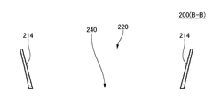
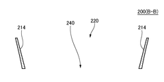
- FIG. 3 is a cross-sectional view taken along the line BB in FIG.
- FIG. 11 is a perspective view of a light emitting device according to Modification 1. It is sectional drawing of the light reflection member shown in FIG. It is sectional drawing of the light reflection member shown in FIG. It is a figure which shows the 1st example of the light distribution based on the modification 1.
- FIG. It is a figure which shows the 1st example of the light distribution based on the modification 1.
- FIG. It is a figure which shows the 2nd example of the light distribution based on the modification 1.
- FIG. It is a figure which shows the 2nd example of the light distribution based on the modification 1.
- FIG. It is a figure which shows the 3rd example of the light distribution based on the modification 1.
- FIG. It is a figure which shows the 3rd example of the light distribution based on the modification 1.
- FIG. It is a perspective view of the light-emitting device concerning the modification 2. It is sectional drawing of the light reflection member shown in FIG. It is sectional drawing of the light reflection member shown in FIG. It is a figure which shows the light distribution in the modification 2.
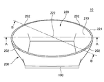
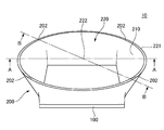
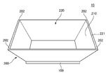
- FIG. 1 is a perspective view showing a configuration of a light emitting device 10 according to an embodiment.
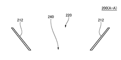
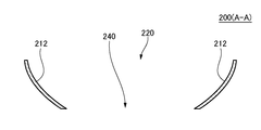
- FIG. 2 is a cross section taken along the line AA in FIG. 1, that is, a cross section that is perpendicular to the one end 220 and does not include the diagonal line of the light emitting member 100.
- 3 is a cross section taken along the line BB in FIG. 1, that is, a cross section that is perpendicular to the one end 220 and includes a corner portion of the light emitting member 100.
- the AA cross section passes through the center of the other end 240 that is a rectangle (that is, the intersection of two diagonal lines of the other end 240) and is parallel to one side of the other end 240. .
- the light emitting device 10 includes a light emitting member 100 and a light reflecting member 200.
- the light reflecting member 200 is a cylindrical member (tubular member), and at least one end 220 is opened.
- the one end 220 of the light reflecting member 200 is circular or elliptical.
- One end 220 has a circumferential portion 221 and a center 222 which is the center point of the circle.
- the light emitting member 100 is a polygon (for example, a rectangle).
- the light emitting member 100 may be disposed in the middle of the cylindrical light reflecting member 200. Further, when the other end 240 of the light reflecting member 200 is closed, the light reflecting member 200 is accommodated inside the light reflecting member 200.
- the light emitting member 100 may be disposed on the bottom surface of the light reflecting member 200.
- the other end 240 of the light reflecting member 200 may be opened.
- the opening of the other end 240 of the light reflecting member 200 is similar to the light emitting member 100.
- the light emitting member 100 and the opening of the other end 240 of the light reflecting member 200 may contact each other without a gap.
- a light non-transparent material such as a resin may be provided in the gap.
- the inner surface 210 of the light reflecting member 200 is inclined in a direction in which the inner surface 210 faces the opening of the one end 220.
- the light reflecting member 200 is a portion in which the inner peripheral shape in the cross section when the inner surface 210 is formed in a plane parallel to the light emitting member 100 is the same as or similar to the light emitting member 100 (hereinafter referred to as a polygonal portion). have.
- the polygonal part is the other end 240 of the light reflecting member 200.
- the inner surface 210 has at least a part of the inner surface 210 between the one end 220 and the above-described polygonal portion as a light reflecting surface.
- the light emitting member 100 is attached to the above-mentioned polygon part in the direction which radiates
- the light emitting member 100 has, for example, a substrate and a light emitting element.
- the light emitting element is formed on one surface of the substrate.
- the substrate is formed of a light transmissive material such as glass or a light transmissive resin.
- the substrate may be formed of a material that does not have translucency.
- the substrate is, for example, a polygon such as a rectangle.
- an inorganic barrier film such as SiN x or SiON is formed on at least the light emitting surface (preferably both surfaces) of the substrate in order to suppress moisture from passing through the substrate.
- the light emitting element is, for example, an organic EL element.
- the light emitting element has a configuration in which a first electrode, an organic layer, and a second electrode are stacked in this order.
- the first electrode is a transparent electrode having optical transparency.
- the transparent conductive material constituting the transparent electrode is a metal-containing material, for example, a metal oxide such as ITO (Indium Tin Oxide), IZO (Indium Zinc Oxide), IWZO (Indium Tungsten Zinc Oxide), ZnO (Zinc Oxide) or the like. is there.
- the thickness of the first electrode is, for example, not less than 10 nm and not more than 500 nm.
- the first electrode is formed using, for example, a sputtering method or a vapor deposition method.
- the first electrode may be a carbon nanotube or a conductive organic material such as PEDOT / PSS.
- the second electrode is, for example, a metal selected from the first group consisting of Al, Au, Ag, Pt, Mg, Sn, Zn, and In, or a metal consisting of an alloy of a metal selected from the first group. Contains layers. In this case, the second electrode has a light shielding property.
- the thickness of the second electrode is, for example, not less than 10 nm and not more than 500 nm. However, the second electrode may be formed using the material exemplified as the material of the first electrode.
- the second electrode is formed using, for example, a sputtering method or a vapor deposition method.
- the materials of the first electrode and the second electrode described above are examples when light is transmitted through the substrate, that is, when light emission from the light emitting device 10 is performed through the substrate (that is, bottom emission type).
- one of two types of stacked structures of a reverse product type and a forward product type can be employed.
- the material of the first electrode and the material of the second electrode are opposite to those of the bottom emission type. That is, the above-described second electrode material is used as the first electrode material, and the above-described first electrode material is used as the second electrode material.
- the first electrode material is formed on the second electrode material, the organic layer is further formed thereon, and the second electrode is formed thinly thereon.
- the light is extracted from the side opposite to the substrate.
- the material for forming the thin film is, for example, the material exemplified as the material for the second electrode or an MgAg alloy.
- the organic layer has, for example, a configuration in which a hole injection layer, a light emitting layer, and an electron injection layer are stacked in this order.
- a hole transport layer may be formed between the hole injection layer and the light emitting layer.
- an electron transport layer may be formed between the light emitting layer and the electron injection layer.
- the organic layer may be formed by a vapor deposition method.
- at least one of the organic layers, for example, a layer in contact with the first electrode may be formed by a coating method such as an inkjet method, a printing method, or a spray method. In this case, the remaining layers of the organic layer are formed by vapor deposition. Further, all layers of the organic layer may be formed using a coating method.
- the light emitting member 100 further has a sealing portion for sealing the light emitting element.
- the sealing portion is formed using, for example, a metal such as glass or aluminum, or a resin, and has a polygonal shape or a circular shape similar to that of the substrate, and has a shape having a recess at the center.
- the edge of the sealing portion is fixed to the substrate with an adhesive. Thereby, the space surrounded by the sealing portion and the substrate is sealed. And the light emission part is located in this sealed space.
- the sealing part may be a sealing film.
- the sealing film is formed of, for example, an insulating material, more specifically, an inorganic material such as aluminum oxide or titanium oxide.
- the thickness of the sealing film is preferably 300 nm or less. Moreover, the thickness of the sealing film is, for example, 50 nm or more.
- the sealing film is formed using, for example, an ALD (Atomic Layer Deposition) method, but may be formed using another film forming method such as a CVD method or a sputtering method.
- the light reflecting member 200 is a cylindrical member, and at least one end 220 is opened to emit light.
- One end 220 is circular or oval. More specifically, when the light emitting member 100 is a regular polygon (for example, a square), the one end 220 is circular, and when the light emitting member 100 is the other case (for example, a rectangular shape), the one end 220 is elliptical. .
- the light reflecting member 200 has a region (hereinafter referred to as a polygonal portion) in which the inner circumference in a cross section parallel to the one end 220 is the same polygon as the light emitting member 100.
- the polygonal portion is provided to hold the light emitting member 100.
- the other end 240 is open and forms the above-described polygonal portion.
- the planar shape of the other end 240 is a square.
- the shape of the light reflecting member 200 when viewed in a cross section parallel to the one end 220 is gradually rounded as the cross section approaches the one end 220 from the other end 240.
- the cross section in the portion closer to the one end 220 than the other end 240 has a corner at the same position as the other end 240.
- the cross section of any portion is circular or elliptical. Does not have a cross-sectional shape.
- the cross section has four corners. The angle of the corner gradually increases as the cross section approaches the one end 220 from the other end 240.
- an inner surface 210 (hereinafter referred to as a first portion 212) of a portion appearing in the AA cross section of FIG. 1, that is, the cross section of FIG. 2, and a BB cross section of FIG.
- the inner surface 210 (hereinafter referred to as the second portion 214) of the portion appearing in the section 3 is a straight line.
- the inclination of the cross section shown in FIG. 2 is gentler than the inclination of the cross section shown in FIG.
- At least a part (preferably all) of the region between the polygonal portion and the one end 220 of the inner surface 210 of the light reflecting member 200 is a light reflecting surface (mirror) that reflects light.
- the other end 240 is a polygonal portion, so that the entire inner surface 210 is a light reflecting surface.
- the light reflecting member 200 has a plurality of intersection points 202 at a circumferential portion 221 of one end 220.
- the number of intersection points 202 matches the number of corners of the polygon.
- Each of the intersection points 202 is on the circumference 221 out of a line connecting the end of a perpendicular line from the corner of the other end 240 (that is, the polygonal portion) to the plane including the one end 220 and the center 222 of the one end 220 with a straight line. This is a point.
- each of the intersection points 202 is an intersection point of a plane perpendicular to the one end 220 and including the center 222 of the one end 220 and the corners of the other end 240 and the circumference 221 of the one end 220.
- the figure formed by connecting all the intersection points 202 along the one end 220 is similar to the other end 240 (in the example shown in FIG. 1, a square).
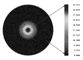
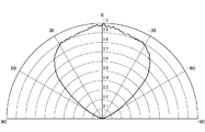
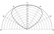
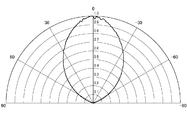
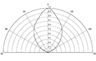
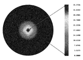
- FIG. 4 and 5 are diagrams showing the light distribution of the light-emitting device 10 shown in FIGS. 1, 2, and 3.
- FIG. 34 and 35 are diagrams illustrating light distributions of the light emitting device 10 according to the comparative example.
- the light reflecting member 200 has a shape in which the bottom surface is cut off from the top of a pyramid similar to the light emitting member 100 to form the other end 240.
- the light reflecting member 200 according to the comparative example has one end 220, the other end 240, and all of the cross sections parallel to the one end 220 that are similar to each other in a polygon (for example, a rectangle).
- FIGS. 4 and 34 show a horizontal light distribution of 180 ° at a location 1 m away from the light emitting member 100
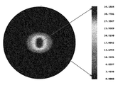
- FIGS. 5 and 35 show a hemisphere with respect to the center of the light emitting member 100 at a location 1 m away from the light emitting member 100.
- Light distribution In any of the drawings, a region corresponding to the center of the light emitting member 100 is a luminance reference point. From the horizontal distribution of FIGS. 4 and 34, the light emitting device 10 having this embodiment has a 1/2 beam angle of about 78 °, and can concentrate the emitted light to the center. Further, from the hemispherical light distribution in FIGS. 5 and 35, it can be seen that the uneven stripes having the luminous intensity appearing in FIG.
- the one end 220 of the light reflecting member 200 is formed into a circular shape, whereby the corner portion of the inner surface 210 is reduced as much as possible to suppress a steep shape change.
- the light distribution can be condensed to the center while making the best use of the light emitting surface, and uneven light distribution can be further suppressed.
- angular part of the light-emitting member 100 can be made smaller than the light-emitting device 10 which concerns on a comparative example. Therefore, according to the present embodiment, the illuminance unevenness is reduced in the region illuminated by the light emitting member 100.
- the light reflecting member 200 has a shape in which the top of the cone is cut off and the other end 240 is formed.
- the light emitting member 100 cannot be properly fitted in the light reflecting member 200.
- the other end 240 is larger than the light emitting member 100, it is necessary to design the other end 240 so that the entire light emitting member 100 can be accommodated, and the diameter is considerably large.
- the light reflecting member 200 is considerably larger than the light emitting member 100, which is not realistic.
- FIG. 6 is a perspective view of the light emitting device 10 according to the first modification, and corresponds to FIG. 1 in the embodiment.
- 7 and 8 are cross-sectional views of the light reflecting member 200 shown in FIG. 7 corresponds to the AA cross section of FIG. 6, and FIG. 8 corresponds to the BB cross section of FIG. 7 corresponds to FIG. 2 in the embodiment, and FIG. 8 corresponds to FIG. 3 in the embodiment.
- the light emitting device 10 according to this modification has the same configuration as the light emitting device 10 according to the embodiment except for the shape of the light reflecting member 200.
- the shape of the light reflecting member 200 when viewed in a cross section parallel to the one end 220 is gradually rounded as the cross section approaches the one end 220 from the other end 240.
- the cross section between the one end 220 and the other end 240 is circular or elliptical, and the cross section in the region closer to the one end 220 is also circular or elliptical.
- at least a portion (first portion 212) shown in a cross section of the inner surface 210 of the light reflecting member 200 that is perpendicular to the one end 220 and does not include the diagonal line of the light emitting member 100 is at least.
- the upper part is a curve.
- a portion (second portion 214) of the inner surface 210 of the light reflecting member 200 that is perpendicular to the one end 220 and shown in a cross section including the corner portion of the light emitting member 100 is the embodiment. As well as a straight line.
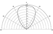
- FIGS. 9 and 10 are diagrams illustrating a first example of the light distribution of the light-emitting device 10 illustrated in FIGS. 6, 7, and 8.
- FIG. 9 corresponds to FIG. 4 of the embodiment
- FIG. 10 corresponds to FIG. 5 of the embodiment.
- the cross section of the light reflecting member 200 is circular or elliptical at the midpoint between the one end 220 and the other end 240 rather than the other end 240.
- the variation in the brightness of the area illuminated by the light emitting member 100 is smaller than that of the comparative example shown in FIGS.
- the region having the same luminous intensity as the center is wider than in the embodiment.
- the 1/2 beam angle is about 102 °.
- it is the shape where the luminous intensity distribution near the center was crushed rather than the thing of embodiment and a comparative example, and it has become uniform luminous intensity in the wide range from the center.
- FIG. 10 it can be seen from FIG. 10 that there is no unevenness in light distribution, and that the luminous intensity is constant over a wide range from the center.
- the light intensity can be made more uniform in a wide range from the center of the light distribution without causing uneven light distribution.
- FIGS. 11 and 12 are diagrams illustrating a second example of the light distribution of the light emitting device 10 illustrated in FIGS. 6, 7, and 8. 11 corresponds to FIG. 4 of the embodiment, and FIG. 12 corresponds to FIG. 5 of the embodiment. Assuming that the height from the other end 240 to the one end 220 is “1”, in the example shown in this figure, the light reflecting member 200 has a circular or oval cross section at a height of 3/4. From FIG. 11, it can be seen that the 1/2 beam angle is about 96 ° in this modification.
- FIG. 13 and 14 are diagrams showing a third example of the light distribution of the light emitting device 10 shown in FIGS. 6, 7, and 8.
- FIG. FIG. 13 corresponds to FIG. 4 of the embodiment
- FIG. 14 corresponds to FIG. 5 of the embodiment.
- the cross section of the light reflecting member 200 is circular or oval at a position where the height is 1/4. From FIG. 13, it can be seen that the 1/2 beam angle is about 142 ° in this modification.
- the light condensing effect on the center of the light emitting device 10 becomes stronger, and the 1/2 beam angle becomes narrower.
- the range of the same luminous intensity increases as the distance from the other end 240 approaches. Therefore, when it is desired to collect light at the center, it is preferable that a portion where the cross section of the light reflecting member 200 is circular or elliptical is close to the one end 220. On the other hand, when it is desired to have the same luminous intensity over a wide range, this portion should be close to the other end 240.
- the characteristics of the light reflecting member 200 can be changed by adjusting the position (height) of the portion where the cross section of the light reflecting member 200 is circular or elliptical.
- (Modification 2) 15 is a perspective view of the light emitting device 10 according to the second modification, and corresponds to FIG. 6 in the first modification.
- 16 and 17 are cross-sectional views of the light reflecting member 200 shown in FIG. 16 corresponds to the AA section of FIG. 15, and FIG. 17 corresponds to the BB section of FIG. That is, FIG. 16 corresponds to FIG. 7 in the first modification, and FIG. 17 corresponds to FIG. 8 in the first modification.
- the light emitting device 10 according to the second modification has the same configuration as the light emitting device 10 according to the first modification, except for the shape of the light reflecting member 200.
- the shape of the light reflecting member 200 when viewed in a cross section parallel to the one end 220 is a portion between the one end 220 and the other end 240 as in the first modification, and the cross section is circular or elliptical.
- the cross section in the region closer to the one end 220 is also circular or elliptical.
- the inner surface 210 (first portion 212) of the light reflecting member 200 in the AA cross section ie, the cross section not including the corner of the other end 240 shown in FIG.
- the inner surface 210 (second portion 214) of the light reflecting member 200 is bent upward. Yes.
- FIG. 18 is a diagram showing a horizontal light distribution of 180 ° at a location 1 m away from the light emitting member 100 in the light emitting device 10 according to this modification.
- the position (height) of the portion where the cross section of the light reflecting member 200 is circular or elliptical is 3/4 from the other end 240.
- the 1/2 beam angle is 86 °.
- the characteristics of the light reflecting member 200 can be changed by adjusting the position (height) of the portion where the cross section of the light reflecting member 200 is circular or oval. .
- FIG. 19 is a perspective view of a light-emitting device 10 according to Modification Example 3, and corresponds to FIG. 1 in the embodiment.
- FIG. 21, and FIG. 22 are cross-sectional views of the light reflecting member 200 shown in FIG. 20 corresponds to the AA section of FIG. 19, and FIG. 21 corresponds to the BB section of FIG. That is, FIG. 20 corresponds to FIG. 2 in the embodiment, and FIG. 21 corresponds to FIG. 3 in the embodiment.
- FIG. 22 is a CC cross section of FIG. 19 (that is, a cross section perpendicular to one end 220 and including the centers of the two long sides of the other end 240).
- the light emitting device 10 according to this modification has the same configuration as that of the light emitting device 10 according to the embodiment except that the other end 240 is rectangular and the shape of the light reflecting member 200 is changed accordingly. It is.
- the portion shown in the cross section of FIG. 20 (first portion 212), the portion shown in the cross section of FIG. 21 (second portion 214), and the cross section of FIG.
- the portion (third portion 216) shown is a straight line.
- FIG. 23 and 24 are diagrams showing a horizontal light distribution of 180 ° at a location 1 m away from the light emitting member 100 in the light emitting device 10 according to this modification.
- FIG. 23 shows the light distribution characteristic in the long side direction (light distribution characteristic in the AA direction)
- FIG. 24 shows the light distribution characteristic in the short side direction (light distribution characteristic in the CC direction).
- the 1 ⁇ 2 beam angle in FIG. 23 is 84 °
- the 1 ⁇ 2 beam angle in FIG. 24 is 76 °.
- FIG. 25 shows a hemispherical light distribution with respect to the center of the light emitting member 100 at a location 1 m away from the light emitting member 100. From this figure, it can be seen that the light intensity near the center is uniform over a wide range in this modification.
- the illuminance unevenness in the region illuminated by the light emitting member 100 is reduced as in the embodiment.
- FIG. 26 is a perspective view of the light emitting device 10 according to the fourth modification, and corresponds to FIG. 19 in the third modification.
- 27, 28, and 29 are cross-sectional views of the light reflecting member 200 shown in FIG. 27 corresponds to FIG. 20 in the third modification, FIG. 28 corresponds to FIG. 21 in the third modification, and FIG. 29 corresponds to FIG. 22 in the third modification.
- the shape of the light reflecting member 200 when viewed in a section parallel to the one end 220 is a circle between the one end 220 and the other end 240.
- the cross section in a region that is elliptical and closer to the one end 220 has the same configuration as that of the light emitting device 10 according to the modified example 3 except that the cross section is circular or elliptical.
- FIG. 31, and FIG. 32 are diagrams showing the light distribution of the light-emitting device 10 according to this modification.
- 30 corresponds to FIG. 23 of the third modification
- FIG. 31 corresponds to FIG. 24 of the third modification
- FIG. 32 corresponds to FIG. 25 of the third modification.
- the 1/2 beam angle in the long side direction is 92 °
- the 1/2 beam angle in the short side direction is 90 °.
- the light intensity in the vicinity of the center becomes uniform in a wider range compared to FIG.
- the characteristics of the light reflecting member 200 are changed by adjusting the position (height) of the portion where the cross section of the light reflecting member 200 is circular or elliptical, as in the first modification. Can be made.
Landscapes
- Engineering & Computer Science (AREA)
- General Engineering & Computer Science (AREA)
- Led Device Packages (AREA)
Abstract
光反射部材(200)の内面(210)は、内面(210)が一端(220)に対向する方向に傾斜している。光反射部材(200)の一端(220)は円形又は楕円形である。光反射部材(200)は、内面(210)に平行な断面における内周の形状が発光部材(100)と同一形状または相似である部分(以下、多角部と記載)を有している。多角部は光反射部材(200)の他端(240)である。また、内面(210)は、内面(210)のうち一端(220)と上記した多角部の間の少なくとも一部が光反射面になっている。そして、発光部材(100)は、上記した多角部に、内面(210)に光を放射する方向に取り付けられている。
Description
本発明は、光反射装置及び発光装置に関する。
発光素子の一つに有機EL素子がある。有機EL素子は、第1電極と第2電極の間に有機層を挟んだ構成を有しているため、面光源にすることができる。一方、発光素子を照明装置として使用する場合、集光効率を向上させることを目的として、発光素子を光反射部材で囲むことが多い。例えば特許文献1には、複数のLEDからなる面光源に、回転放物面からなる筒状の光反射部材を取り付けることが記載されている。
有機EL素子は製造効率・コストの観点から、いわゆる大判で作成してから、所望のサイズのパネルにスクライブ(裁断)するというプロセスで製造されることが多い。大判から切り取るため取出し枚数の都合上、有機EL素子の形状は多角形(例えば矩形)である場合が多い。また、製造プロセスの効率上、大判自体も多角形である場合が多い。他方で、従来がたの点光源のような光装置の発光を集光あるいは分光する光反射装置としては、円筒形の光反射装置が知られている。面光源である有機EL素子が多角形である場合、円筒形の光反射装置を用いると照明装置によって照明される領域には、有機EL素子の角部の存在に起因して、配光分布の光度変化が不均一な部分が発生し、照明される領域において照度ムラができてしまう。本発明者は、多角形の有機EL素子を発光装置の発光部材として使用する場合において、光反射部材の形状を工夫することにより、有機EL素子によって照明される領域の照度変化が均等となり、照度ムラが生じないようにすることを検討した。
本発明が解決しようとする課題としては、多角形の有機EL素子を発光装置の発光部材として使用する場合において、光反射部材の形状を工夫することにより、有機EL素子によって照明される領域の照度変化を均等として、照度ムラが生じないようにすることが一例として挙げられる。
請求項1に記載の発明は、少なくとも一端が開口している筒部材を備え、
前記筒部材の内面は、前記内面が前記一端の開口に対向する方向に傾斜しており、
前記一端は円形又は楕円形であり、
前記筒部材は、前記一端に平行な断面における内周が多角形である多角部を有しており、かつ、前記内面のうち前記一端と前記多角部の間の少なくとも一部が光反射面である光反射装置である。
前記筒部材の内面は、前記内面が前記一端の開口に対向する方向に傾斜しており、
前記一端は円形又は楕円形であり、
前記筒部材は、前記一端に平行な断面における内周が多角形である多角部を有しており、かつ、前記内面のうち前記一端と前記多角部の間の少なくとも一部が光反射面である光反射装置である。
請求項10に記載の発明は、少なくとも一端が開口している筒部材と
前記筒部材の内部に収容され、多角形である発光部材と、
を備え、
前記筒部材の内面は、前記内面が前記一端の開口に対向する方向に傾斜しており、
前記一端は円形又は楕円形であり、
前記筒部材は、前記一端に平行な断面における内周が前記多角形と同一または相似である多角部を有しており、かつ、前記内面のうち前記一端と前記多角部の間の少なくとも一部が光反射面であり、
前記発光部材は、前記多角部に、前記一端に光を放射する方向に取り付けられている発光装置である。
前記筒部材の内部に収容され、多角形である発光部材と、
を備え、
前記筒部材の内面は、前記内面が前記一端の開口に対向する方向に傾斜しており、
前記一端は円形又は楕円形であり、
前記筒部材は、前記一端に平行な断面における内周が前記多角形と同一または相似である多角部を有しており、かつ、前記内面のうち前記一端と前記多角部の間の少なくとも一部が光反射面であり、
前記発光部材は、前記多角部に、前記一端に光を放射する方向に取り付けられている発光装置である。
上述した目的、およびその他の目的、特徴および利点は、以下に述べる好適な実施の形態、およびそれに付随する以下の図面によってさらに明らかになる。
以下、本発明の実施の形態について、図面を用いて説明する。尚、すべての図面において、同様な構成要素には同様の符号を付し、適宜説明を省略する。
図1は、実施形態に係る発光装置10の構成を示す斜視図である。図2は図1のA-A断面、すなわち一端220に垂直であり、かつ発光部材100の対角線を含まない断面である。図3は図1のB-B断面、すなわち一端220に垂直であり、かつ発光部材100の角部を含む断面である。なお、本図に示す例において、A-A断面は、矩形である他端240の中心(すなわち他端240の2つの対角線の交点)を通っており、かつ他端240の一辺と平行である。
実施形態に係る発光装置10は、発光部材100及び光反射部材200を有している。光反射部材200は筒状の部材(筒部材)であり、少なくとも一端220が開口している。また、光反射部材200の一端220は円形又は楕円形である。一端220は円周部分221と円の中心点である中心222を有する。発光部材100は多角形(例えば矩形)である。発光部材100は筒状の光反射部材200の途中に配置されていてもよい。また、光反射部材200の他端240が閉口している場合は、光反射部材200の内部に収容されている。この際、発光部材100は光反射部材200の底面に配置されていてもよい。他方、光反射部材200の他端240は開口していてもよく、その場合、光反射部材200の他端240の開口は発光部材100と相似形になっている。この場合、発光部材100と光反射部材200の他端240の開口とは隙間なく接してもよい。また、発光部材100と光反射部材200との間に隙間がある場合、この隙間に樹脂などの光非透過性の材料を設けてもよい。光反射部材200の内面210は、内面210が一端220の開口に対向する方向に傾斜している。光反射部材200は、内面210を発光部材100に平行な面で断面を形成した場合の当該断面における内周の形状が発光部材100と同一形状または相似である部分(以下、多角部と記載)を有している。図1、図2、及び図3に示す例において、多角部は光反射部材200の他端240である。また、内面210は、内面210のうち一端220と上記した多角部の間の少なくとも一部が光反射面になっている。そして、発光部材100は、上記した多角部に、内面210に光を放射する方向に取り付けられている。以下、詳細に説明する。
発光部材100は、例えば基板及び発光素子を有している。発光素子は基板の一面の上に形成されている。
発光素子がボトムエミッション型である場合、基板は、例えばガラスや透光性の樹脂などの透光性の材料で形成されている。ただし、発光素子がトップエミッション型である場合、基板は透光性を有さない材料で形成されていてもよい。基板は、例えば矩形などの多角形である。また、基板が樹脂材料を含む場合、水分が基板を透過することを抑制するために、基板の少なくとも発光面(好ましくは両面)に、SiNxやSiONなどの無機バリア膜が形成されている。
発光素子は、例えば有機EL素子である。この場合、発光素子は、第1電極、有機層、及び第2電極をこの順に積層させた構成を有している。
第1電極は、光透過性を有する透明電極である。透明電極を構成する透明導電材料は、金属を含む材料、例えば、ITO(Indium Tin Oxide)、IZO(Indium Zinc Oxide)、IWZO(Indium Tungsten Zinc Oxide)、ZnO(Zinc Oxide)等の金属酸化物である。第1電極の厚さは、例えば10nm以上500nm以下である。第1電極は、例えばスパッタリング法又は蒸着法を用いて形成される。なお、第1電極は、カーボンナノチューブ、又はPEDOT/PSSなどの導電性有機材料であってもよい。
第2電極は、例えば、Al、Au、Ag、Pt、Mg、Sn、Zn、及びInからなる第1群の中から選択される金属又はこの第1群から選択される金属の合金からなる金属層を含んでいる。この場合、第2電極は遮光性を有している。第2電極の厚さは、例えば10nm以上500nm以下である。ただし、第2電極は、第1電極の材料として例示した材料を用いて形成されていてもよい。第2電極は、例えばスパッタリング法又は蒸着法を用いて形成される。
なお、上記した第1電極及び第2電極の材料は、基板を光が透過する場合、すなわち発光装置10からの発光が基板を透過して行われる場合(すなわちボトムエミッション型)の例である。発光装置10からの発光が基板を透過しないで行われる場合(トップエミッション型)、逆積型と、順積型との2種類の積層構造のいずれかを採用できる。逆積型では、第1電極の材料と第2電極の材料はボトムエミッション型と逆になる。すなわち第1電極の材料には上記した第2電極の材料が用いられ、第2電極の材料には上記した第1電極の材料が用いられる。他方の順積型では、上記した第2電極の材料の上に第1電極の材料を形成し、更にその上に有機層、さらにその上に薄く成膜した第2電極を形成することで、基板とは逆側から光を取出す構造である。なお、薄く成膜する材料は、例えば第2電極の材料として例示した材料やMgAg合金などである。
有機層は、例えば、正孔注入層、発光層、及び電子注入層をこの順に積層させた構成を有している。正孔注入層と発光層との間には正孔輸送層が形成されていてもよい。また、発光層と電子注入層との間には電子輸送層が形成されていてもよい。有機層は蒸着法で形成されてもよい。また、有機層のうち少なくとも一つの層、例えば第1電極と接触する層は、インクジェット法、印刷法、又はスプレー法などの塗布法によって形成されてもよい。なお、この場合、有機層の残りの層は、蒸着法によって形成されている。また、有機層のすべての層が、塗布法を用いて形成されていてもよい。
発光部材100は、さらに、発光素子を封止する封止部を有している。封止部は、例えばガラス、アルミニウムなどの金属、又は樹脂を用いて形成されており、基板と同様の多角形や円形であり、中央に凹部を設けた形状を有している。そして封止部の縁は接着材で基板に固定されている。これにより、封止部と基板で囲まれた空間は封止される。そして発光部は、この封止された空間の中に位置している。
封止部は封止膜であってもよい。封止膜は、例えば絶縁材料、さらに具体的には酸化アルミニウムや酸化チタンなどの無機材料によって形成されている。封止膜の厚さは、好ましくは300nm以下である。また、封止膜の厚さは、例えば50nm以上である。封止膜は、例えばALD(Atomic Layer Deposition)法を用いて形成されているが、他の成膜法、例えばCVD法やスパッタリング法を用いて形成されていてもよい。
光反射部材200は、筒状の部材であり、少なくとも一端220は、光を放射するために開口している。一端220は円形又は楕円である。より詳細には、発光部材100が正多角形(例えば正方形)である場合、一端220は円形であり、発光部材100がそれ以外の場合(例えば長方形)である場合、一端220は楕円形である。
光反射部材200は、一端220に平行な断面における内周が発光部材100と同一の多角形となる領域(以下、多角部と記載)を有している。多角部は、発光部材100を保持するために設けられている。図1、図2、及び図3に示す例において、他端240は開口しており、上記した多角部となっている。また、図1、図2、及び図3に示す例において、他端240の平面形状は正方形である。
光反射部材200を一端220に平行な断面で見たときの形状は、断面が他端240から一端220に近づくにつれて徐々に丸みを帯びていく。ただし、他端240よりも一端220に近い部分における断面は、いずれも他端240と同様の位置に角を有している。このため、光反射部材200は、他端240(すなわち多角部)から一端220までの間で、一端220に平行な断面を形成した場合には、どの部分の断面においても円形または楕円形となる断面形状を有していない。図1に示す例において、当該断面は、4つの角を有しているが、この角の角度は、当該断面が他端240から一端220に近づくにつれて、徐々に大きくなっている。
そして、光反射部材200のうち、図1のA-A断面、つまり図2の断面に現れる部分の内面210(以下、第1部分212と記載)、及び図1のB-B断面、つまり図3の断面に現れる部分の内面210(以下、第2部分214と記載)は、いずれも直線である。ただし、図2に示した断面の傾斜のほうが、図3に示した断面の傾斜よりも緩やかである。
また、光反射部材200の内面210のうち、少なくとも多角部と一端220の間の領域の少なくとも一部(好ましくは全部)は、光を反射する光反射面(鏡)になっている。図1、図2、及び図3に示す例では他端240が多角部となっているため、内面210の全体が光反射面になっている。
また、図1に示すように、光反射部材200は一端220の円周部分221に複数の交点202を有する。交点202の数は、多角部の角の数と一致している。交点202は、いずれも、他端240(すなわち多角部)の角から一端220を含む面に下した垂線の端部と、一端220の中心222とを直線で結んだ線のうち円周221上にある点である。換言すれば、交点202は、いずれも、一端220に垂直かつ一端220の中心222及び他端240の角を含む面と、一端220の円周221との交点である。すべての交点202を一端220に沿って結ぶことにより形成される図形は、他端240と相似(図1に示す例では正方形)である。
図4及び図5は、図1、図2、及び図3に示した発光装置10の配光分布を示す図である。図34及び図35は、比較例に係る発光装置10の配光分布を示す図である。比較例において、光反射部材200は、図33に示すように、底面が発光部材100と相似の角錐の頂部を切り落として他端240とした形状を有している。言い換えると、比較例に係る光反射部材200は、一端220、他端240、及び一端220に平行な断面のすべてが互いに相似な多角形(例えば矩形)となっている。そして図4及び図34は、発光部材100から1m離れた場所における水平180°の配光分布であり、図5及び図35は、発光部材100から1m離れた場所における発光部材100の中央に対する半球状の配光分布である。いずれの図においても、発光部材100の中心に対応する領域が輝度の基準点となっている。図4と図34の水平方向分布より、本実施形態を有する発光装置10は1/2ビーム角が78°程度となっており、発光をより中央へと集光することができる。また、図5と図35の半球配光分布より、比較例の図35に現れている光度が他の領域よりも高いスジムラが軽減されていることがわかる。これは、光反射部材200の一端220を円形状としたことにより内面210において、角部分を極力減らし、急峻な形状の変化を抑えたためである。これにより発光面を最大限活用したまま配光を中央へと集光させることができ、さらに配光ムラを抑えることができる。
そして、このように実施形態に係る発光装置10では、比較例に係る発光装置10よりも、発光部材100の角部に対応した光度変化の不均一な部分を小さくできる。従って、本実施形態によれば、発光部材100によって照明される領域において照度ムラが小さくなる。
なお、光反射部材200を、円錐の頂部を切り落として他端240とした形状にすることも考えられる。しかし、この場合、光反射部材200に発光部材100をきちんと嵌め込むことができない。このため、他端240が発光部材100よりも大きい場合、他端240の径は発光部材100が全て収まるように設計する必要があり、かなり大きな径となってしまう。結果として光反射部材200が発光部材100よりもかなり大きくなり現実的ではない。
(変形例1)
図6は、変形例1に係る発光装置10の斜視図であり、実施形態における図1に対応している。図7及び図8は、図6に示した光反射部材200の断面図である。図7は図6のA-A断面に対応しており、図8は図6のB-B断面に対応している。すなわち図7は実施形態における図2に対応しており、図8は実施形態における図3に対応している。本変形例に係る発光装置10は、光反射部材200の形状を除いて、実施形態に係る発光装置10と同様の構成である。
図6は、変形例1に係る発光装置10の斜視図であり、実施形態における図1に対応している。図7及び図8は、図6に示した光反射部材200の断面図である。図7は図6のA-A断面に対応しており、図8は図6のB-B断面に対応している。すなわち図7は実施形態における図2に対応しており、図8は実施形態における図3に対応している。本変形例に係る発光装置10は、光反射部材200の形状を除いて、実施形態に係る発光装置10と同様の構成である。
本変形例においても、一端220に平行な断面で見たときの光反射部材200の形状は、断面が他端240から一端220に近づくにつれて徐々に丸みを帯びていく。ただし、一端220と他端240の間において断面は円形又は楕円になり、それより一端220に近い領域での断面も、円形又は楕円である。このため、図7に示すように、光反射部材200の内面210のうち、一端220に垂直であり、かつ発光部材100の対角線を含まない断面に示される部分(第1部分212)は、少なくとも上部が曲線である。一方、図7に示すように、光反射部材200の内面210のうち、一端220に垂直であり、かつ発光部材100の角部を含む断面に示される部分(第2部分214)は、実施形態と同様に直線である。
図9及び図10は、図6、図7、及び図8に示した発光装置10の配光分布の第1例を示す図である。図9は実施形態の図4に対応しており、図10は実施形態の図5に対応している。本図に示す例において、光反射部材200の断面は、他端240よりも、一端220と他端240の中間点で円形又は楕円になっている。本図から明らかなように、本変形例によっても、実施形態と同様に、発光部材100によって照明される領域の明るさのばらつきは、図34及び図35に示した比較例よりも小さくなる。
また、本例によれば、中心と同程度の光度となっている領域は、実施形態よりも広がっている。具体的には、図9より、1/2ビーム角は約102°程度となっていることがわかる。また、実施形態や比較例のものよりも中央付近の光度分布がつぶれた形状となっており、中央から広い範囲において均一な光度となっていることがわかる。さらに、図10より、配光のムラも見られず、さらに中心から広い範囲で光度が一定になっていることがわかる。以上より、変形例1の第1例に係る発光装置10によれば、配光ムラを発生させずに、配光の中心から広い範囲で光度をより均一にできる。
図11及び図12は、図6、図7、及び図8に示した発光装置10の配光分布の第2例を示す図である。図11は実施形態の図4に対応しており、図12は実施形態の図5に対応している。他端240から一端220までの高さを「1」とすると、本図に示す例では高さが3/4の位置で光反射部材200の断面が円形又は楕円になっている。図11より、本変形例では1/2ビーム角は約96°であることがわかる。
また、図13及び図14は、図6、図7、及び図8に示した発光装置10の配光分布の第3例を示す図である。図13は実施形態の図4に対応しており、図14は実施形態の図5に対応している。本図に示す例では高さが1/4の位置で光反射部材200の断面が円形又は楕円になっている。図13より、本変形例では1/2ビーム角は約142°であることがわかる。
以上のことから、光反射部材200の断面が円形又は楕円になる部分を一端220に近づけると発光装置10の中央への集光効果が強くなり1/2ビーム角が狭くなり、逆にこの部分を他端240に近づけると同程度の光度の範囲が広くなっていくことがわかる。従って、中央へ集光させたい場合には、光反射部材200の断面が円形又は楕円になる部分を一端220に近づけるのがよい。一方、広い範囲で同じ光度にしたい場合にはこの部分を他端240に近づけるのがよい。このように、光反射部材200の断面が円形又は楕円になる部分の位置(高さ)を調整すると、光反射部材200の特性を変化させることができる。
(変形例2)
図15は、変形例2に係る発光装置10の斜視図であり、変形例1における図6に対応している。図16及び図17は、図15に示した光反射部材200の断面図である。図16は図15のA-A断面に対応しており、図17は図15のB-B断面に対応している。すなわち図16は変形例1における図7に対応しており、図17は変形例1における図8に対応している。本変形例2に係る発光装置10は、光反射部材200の形状を除いて、変形例1に係る発光装置10と同様の構成である。
図15は、変形例2に係る発光装置10の斜視図であり、変形例1における図6に対応している。図16及び図17は、図15に示した光反射部材200の断面図である。図16は図15のA-A断面に対応しており、図17は図15のB-B断面に対応している。すなわち図16は変形例1における図7に対応しており、図17は変形例1における図8に対応している。本変形例2に係る発光装置10は、光反射部材200の形状を除いて、変形例1に係る発光装置10と同様の構成である。
本図に示す例においても、一端220に平行な断面で見たときの光反射部材200の形状は、変形例1と同様に、一端220と他端240の間の部分で断面は円形又は楕円になり、それより一端220に近い領域での断面も、円形又は楕円である。ただし、円(又は楕円)の径を調整することにより、図16に示したA-A断面(すなわち他端240の角を含まない断面)において、光反射部材200の内面210(第1部分212)は直線となっている。その結果、図17に示したB-B断面(すなわち他端240の2つの角を含む断面)において、光反射部材200の内面210(第2部分214)は、上部が外側に向けて曲がっている。
図18は、本変形例に係る発光装置10における、発光部材100から1m離れた場所における水平180°の配光分布を示す図である。本例において、光反射部材200の断面が円形又は楕円になる部分の位置(高さ)は、他端240から3/4である。本例において、1/2ビーム角は86°となっている。
本変形例によっても、変形例1と同様に、光反射部材200の断面が円形又は楕円になる部分の位置(高さ)を調整することにより、光反射部材200の特性を変化させることができる。
(変形例3)
図19は、変形例3に係る発光装置10の斜視図であり、実施形態における図1に対応している。図20、図21、及び図22は、図19に示した光反射部材200の断面図である。図20は図19のA-A断面に対応しており、図21は図19のB-B断面に対応している。すなわち図20は実施形態における図2に対応しており、図21は実施形態における図3に対応している。また、図22は図19のC-C断面(すなわち一端220に垂直であり、かつ他端240の2つの長辺それぞれの中心を含む断面)である。本変形例に係る発光装置10は、他端240が長方形である点、及びこれに伴って光反射部材200の形状が変わっている点を除いて、実施形態に係る発光装置10と同様の構成である。
図19は、変形例3に係る発光装置10の斜視図であり、実施形態における図1に対応している。図20、図21、及び図22は、図19に示した光反射部材200の断面図である。図20は図19のA-A断面に対応しており、図21は図19のB-B断面に対応している。すなわち図20は実施形態における図2に対応しており、図21は実施形態における図3に対応している。また、図22は図19のC-C断面(すなわち一端220に垂直であり、かつ他端240の2つの長辺それぞれの中心を含む断面)である。本変形例に係る発光装置10は、他端240が長方形である点、及びこれに伴って光反射部材200の形状が変わっている点を除いて、実施形態に係る発光装置10と同様の構成である。
本変形例において、光反射部材200の内面210のうち図20の断面に示される部分(第1部分212)、図21の断面に示される部分(第2部分214)、及び図22の断面に示される部分(第3部分216)は、いずれも直線である。
図23及び図24は、本変形例に係る発光装置10における、発光部材100から1m離れた場所における水平180°の配光分布を示す図である。図23は、長辺方向の配光特性(A-A方向の配光特性)を示しており、図24は短辺方向の配光特性(C-C方向の配光特性)を示している。図23における1/2ビーム角は84°であり、図24における1/2ビーム角は76°である。
図25は、発光部材100から1m離れた場所における発光部材100の中央に対する半球状の配光分布である。本図から、本変形例において中央付近の光度が広い範囲で均一となっていることがわかる。
以上の通り、本変形例によっても、実施形態と同様に、発光部材100によって照明される領域の照度ムラは、小さくなる。
(変形例4)
図26は、変形例4に係る発光装置10の斜視図であり、変形例3における図19に対応している。図27、図28、及び図29は、図26に示した光反射部材200の断面図である。図27は変形例3における図20に対応しており、図28は変形例3における図21に対応しており、図29は変形例3における図22に対応している。本変形例に係る発光装置10は、変形例1と同様に、一端220に平行な断面で見たときの光反射部材200の形状が、一端220と他端240の間の部分で断面は円形又は楕円になり、それより一端220に近い領域での断面も、円形又は楕円である点を除いて、変形例3に係る発光装置10と同様の構成である。
図26は、変形例4に係る発光装置10の斜視図であり、変形例3における図19に対応している。図27、図28、及び図29は、図26に示した光反射部材200の断面図である。図27は変形例3における図20に対応しており、図28は変形例3における図21に対応しており、図29は変形例3における図22に対応している。本変形例に係る発光装置10は、変形例1と同様に、一端220に平行な断面で見たときの光反射部材200の形状が、一端220と他端240の間の部分で断面は円形又は楕円になり、それより一端220に近い領域での断面も、円形又は楕円である点を除いて、変形例3に係る発光装置10と同様の構成である。
そして、光反射部材200の内面210のうち図27の断面に示される部分(第1部分212)及び図29の断面に示される部分(第3部分216)は、少なくとも一部(例えば上部)に曲線となる部分を有しているが、図28の断面に示される部分(第2部分214)は、直線である。
図30、図31、及び図32は、本変形例に係る発光装置10の配光分布を示す図である。図30は変形例3の図23に対応しており、図31は変形例3の図24に対応しており、図32は変形例3の図25に対応している。図30すなわち長辺方向の1/2ビーム角は92°であり、図31すなわち短辺方向の1/2ビーム角は90°である。また、図32に示すように、変形例1と同様に途中で楕円になることで、図25と比較して中央付近の光度がさらに広い範囲で均一となる。
このように、本変形例によっても、変形例1と同様に、光反射部材200の断面が円形又は楕円になる部分の位置(高さ)を調整することにより、光反射部材200の特性を変化させることができる。
以上、図面を参照して実施形態及び実施例について述べたが、これらは本発明の例示であり、上記以外の様々な構成を採用することもできる。
Claims (10)
- 少なくとも一端が開口している筒部材を備え、
前記筒部材の内面は、前記内面が前記一端の開口に対向する方向に傾斜しており、
前記一端は円形又は楕円形であり、
前記筒部材は、前記一端に平行な断面における内周が多角形である多角部を有しており、かつ、前記内面のうち前記一端と前記多角部の間の少なくとも一部が光反射面である光反射装置。 - 請求項1に記載の光反射装置において、
前記筒部材の他端が前記多角形である光反射装置。 - 請求項2に記載の光反射装置において、
前記他端は開口している光反射装置。 - 請求項1~3のいずれか一項に記載の光反射装置において、
前記筒部材は、前記多角部と前記一端との間に、前記一端に平行な断面が円形または楕円形となる領域を有していない光反射装置。 - 請求項1~4のいずれか一項に記載の光反射装置において、
前記一端に垂直であり前記多角部の角を含む断面、及び前記一端に垂直であり前記多角部の角を含まない断面のいずれにおいても、前記筒部材は直線である光反射装置。 - 請求項1~3のいずれか一項に記載の光反射装置において、
前記筒部材は、前記多角部と前記一端との間に、前記一端に平行な断面が円形または楕円形となる領域を有している光反射装置。 - 請求項6に記載の光反射装置において、
前記一端に垂直であり前記多角部の角を含む断面において、前記筒部材は直線であり、
前記一端に垂直であり前記多角部の角を含まない断面において、前記筒部材は曲線となる領域を有している光反射装置。 - 請求項1~7のいずれか一項に記載の光反射装置において、
前記多角部の複数の角のそれぞれにおいて、前記一端に垂直であり前記角を含む断面と前記一端との交点を形成した場合、すべての前記交点を前記一端に沿って結ぶことにより形成される図形は、前記多角形と相似である光反射装置。 - 請求項8に記載の光反射装置において、
前記多角形は正方形である光反射装置。 - 少なくとも一端が開口している筒部材と
前記筒部材の内部に収容され、多角形である発光部材と、
を備え、
前記筒部材の内面は、前記内面が前記一端の開口に対向する方向に傾斜しており、
前記一端は円形又は楕円形であり、
前記筒部材は、前記一端に平行な断面における内周が前記多角形と同一または相似である多角部を有しており、かつ、前記内面のうち前記一端と前記多角部の間の少なくとも一部が光反射面であり、
前記発光部材は、前記多角部に、前記一端に光を放射する方向に取り付けられている発光装置。
Priority Applications (2)
| Application Number | Priority Date | Filing Date | Title |
|---|---|---|---|
| PCT/JP2015/069190 WO2017002267A1 (ja) | 2015-07-02 | 2015-07-02 | 光反射装置及び発光装置 |
| JP2017525779A JPWO2017002267A1 (ja) | 2015-07-02 | 2015-07-02 | 光反射装置及び発光装置 |
Applications Claiming Priority (1)
| Application Number | Priority Date | Filing Date | Title |
|---|---|---|---|
| PCT/JP2015/069190 WO2017002267A1 (ja) | 2015-07-02 | 2015-07-02 | 光反射装置及び発光装置 |
Publications (1)
| Publication Number | Publication Date |
|---|---|
| WO2017002267A1 true WO2017002267A1 (ja) | 2017-01-05 |
Family
ID=57608150
Family Applications (1)
| Application Number | Title | Priority Date | Filing Date |
|---|---|---|---|
| PCT/JP2015/069190 Ceased WO2017002267A1 (ja) | 2015-07-02 | 2015-07-02 | 光反射装置及び発光装置 |
Country Status (2)
| Country | Link |
|---|---|
| JP (1) | JPWO2017002267A1 (ja) |
| WO (1) | WO2017002267A1 (ja) |
Citations (3)
| Publication number | Priority date | Publication date | Assignee | Title |
|---|---|---|---|---|
| JP2003518272A (ja) * | 1999-12-20 | 2003-06-03 | コジェント・ライト・テクノロジーズ・インコーポレイテッド | 低融点の光ファイバへの高強度の光の結合 |
| JP2005070443A (ja) * | 2003-08-25 | 2005-03-17 | Olympus Corp | 光学装置、照明装置及びプロジェクタ |
| JP2007311357A (ja) * | 1998-06-04 | 2007-11-29 | Seiko Epson Corp | プロジェクタ |
Family Cites Families (2)
| Publication number | Priority date | Publication date | Assignee | Title |
|---|---|---|---|---|
| WO2009028090A1 (ja) * | 2007-08-31 | 2009-03-05 | Phoenix Electric Co., Ltd. | 照明用の発光装置 |
| DE102012009539B4 (de) * | 2012-03-29 | 2020-12-24 | Auer Lighting Gmbh | Leuchte |
-
2015
- 2015-07-02 JP JP2017525779A patent/JPWO2017002267A1/ja active Pending
- 2015-07-02 WO PCT/JP2015/069190 patent/WO2017002267A1/ja not_active Ceased
Patent Citations (3)
| Publication number | Priority date | Publication date | Assignee | Title |
|---|---|---|---|---|
| JP2007311357A (ja) * | 1998-06-04 | 2007-11-29 | Seiko Epson Corp | プロジェクタ |
| JP2003518272A (ja) * | 1999-12-20 | 2003-06-03 | コジェント・ライト・テクノロジーズ・インコーポレイテッド | 低融点の光ファイバへの高強度の光の結合 |
| JP2005070443A (ja) * | 2003-08-25 | 2005-03-17 | Olympus Corp | 光学装置、照明装置及びプロジェクタ |
Also Published As
| Publication number | Publication date |
|---|---|
| JPWO2017002267A1 (ja) | 2018-04-05 |
Similar Documents
| Publication | Publication Date | Title |
|---|---|---|
| US9379357B2 (en) | Organic light emitting structure | |
| JP5480567B2 (ja) | 有機発光素子 | |
| JP2012513084A (ja) | 透明有機発光ダイオード | |
| JP2007080579A (ja) | 面発光装置 | |
| JP2013200964A (ja) | 発光装置 | |
| JP2010272327A (ja) | 有機elパネル | |
| JP5138569B2 (ja) | 有機el発光装置 | |
| JP2014191329A (ja) | 両面表示装置 | |
| WO2017002267A1 (ja) | 光反射装置及び発光装置 | |
| CN103972346A (zh) | 顶面出光率高侧面出光率低的面光源器件 | |
| JP2016021286A (ja) | 照明装置 | |
| US20230320128A1 (en) | Light-emitting device and light-emitting system | |
| CN204230304U (zh) | 发光模块及照明器具 | |
| CN106605307A (zh) | 光源 | |
| JP5891962B2 (ja) | 面発光体 | |
| US20150001491A1 (en) | Light Emitting Panel and Lighting Apparatus | |
| US20160308167A1 (en) | Organic light-emitting element | |
| JP7240478B2 (ja) | 発光装置 | |
| JP2015179584A (ja) | 発光素子 | |
| JP2018206583A (ja) | 発光装置 | |
| JP2016021285A (ja) | 照明装置 | |
| JP6450124B2 (ja) | 発光装置 | |
| WO2013161001A1 (ja) | 有機el発光素子 | |
| JP6528513B2 (ja) | 面発光モジュール | |
| JP2017022073A (ja) | El素子用封止材、el素子、および照明装置 |
Legal Events
| Date | Code | Title | Description |
|---|---|---|---|
| 121 | Ep: the epo has been informed by wipo that ep was designated in this application |
Ref document number: 15897194 Country of ref document: EP Kind code of ref document: A1 |
|
| ENP | Entry into the national phase |
Ref document number: 2017525779 Country of ref document: JP Kind code of ref document: A |
|
| NENP | Non-entry into the national phase |
Ref country code: DE |
|
| 122 | Ep: pct application non-entry in european phase |
Ref document number: 15897194 Country of ref document: EP Kind code of ref document: A1 |