WO2016199307A1 - 光学特性検出光学系、測定プローブおよび光学特性検出装置 - Google Patents
光学特性検出光学系、測定プローブおよび光学特性検出装置 Download PDFInfo
- Publication number
- WO2016199307A1 WO2016199307A1 PCT/JP2015/067089 JP2015067089W WO2016199307A1 WO 2016199307 A1 WO2016199307 A1 WO 2016199307A1 JP 2015067089 W JP2015067089 W JP 2015067089W WO 2016199307 A1 WO2016199307 A1 WO 2016199307A1
- Authority
- WO
- WIPO (PCT)
- Prior art keywords
- light
- detection
- optical
- unit
- refractive index
- Prior art date
- Legal status (The legal status is an assumption and is not a legal conclusion. Google has not performed a legal analysis and makes no representation as to the accuracy of the status listed.)
- Ceased
Links
Images



Classifications
-
- G—PHYSICS
- G01—MEASURING; TESTING
- G01N—INVESTIGATING OR ANALYSING MATERIALS BY DETERMINING THEIR CHEMICAL OR PHYSICAL PROPERTIES
- G01N21/00—Investigating or analysing materials by the use of optical means, i.e. using sub-millimetre waves, infrared, visible or ultraviolet light
- G01N21/17—Systems in which incident light is modified in accordance with the properties of the material investigated
- G01N21/41—Refractivity; Phase-affecting properties, e.g. optical path length
-
- G—PHYSICS
- G01—MEASURING; TESTING
- G01N—INVESTIGATING OR ANALYSING MATERIALS BY DETERMINING THEIR CHEMICAL OR PHYSICAL PROPERTIES
- G01N21/00—Investigating or analysing materials by the use of optical means, i.e. using sub-millimetre waves, infrared, visible or ultraviolet light
- G01N21/17—Systems in which incident light is modified in accordance with the properties of the material investigated
- G01N21/55—Specular reflectivity
- G01N21/552—Attenuated total reflection
Definitions
- the present invention relates to an optical characteristic detection optical system used when detecting the refractive index of a test object such as a living body, a measurement probe including the optical characteristic detection optical system, and an optical characteristic detection device.
- the refractive index of the test object is obtained using the attenuated total reflection method or the surface plasmon resonance method, and the characteristics of the test object are determined based on the obtained refractive index.
- Devices for analysis are known.
- the attenuated total reflection method or surface plasmon resonance method information on the angle of incidence of light on the test surface of the specimen is usually obtained, and the total reflection critical angle or plasmon resonance angle is calculated based on the obtained angle of incidence information.
- the optical characteristics of the test object are analyzed using either the calculation method for calculating the wavelength, the wavelength information, and the calculation method for calculating the total reflection critical angle or the plasmon resonance angle based on the acquired wavelength information. That is, in the attenuated total reflection method or the surface plasmon resonance method, a method of acquiring either the incident angle information or the wavelength information is common.
- Patent Document 1 describes a technique for analyzing the characteristics of a test object by simultaneously acquiring incident angle information and wavelength information.
- a white light source a prism with a test object attached to the bottom surface, a spectral slit, a spectroscope, a two-dimensional photodetector, which are arranged in parallel with the angular spread direction of the reflected light reflected from the prism, And analyzing the characteristics of the test object by obtaining a two-dimensional image showing the incident angle information and the wavelength information at the same time.
- the penetration depth of the evanescent wave on the detection surface used for detection greatly depends on the wavelength. Therefore, when only the incident angle information is acquired, there is a problem that it is not possible to deal with test objects of various sizes in the measurement at a single wavelength.
- the calculation method for calculating the total reflection critical angle or the plasmon resonance angle based on the wavelength information requires a spectroscope and a high-intensity white light source, which increases the size of the apparatus. was there.
- the present invention has been made in view of the above, and an optical characteristic detection optical system, a measurement probe, and an optical characteristic detection that can be downsized even when incident angle information and wavelength information are acquired simultaneously.
- An object is to provide an apparatus.
- an optical characteristic detection optical system includes a light source unit in which a plurality of light emitting points that emit light having different wavelength bands are arranged, and a predetermined refraction.
- a detection unit having a detection surface that is formed by using a member having a rate and that contacts a test object; and a first optical member that condenses light emitted from each of the plurality of light emission points on the detection surface;
- a light receiving unit capable of receiving light from the detection surface, and a second optical member for guiding light from the detection surface to the light receiving unit.
- the detection unit is characterized in that a metal film is formed on the detection surface.
- the optical characteristic detection optical system is the above invention, wherein the incident angle of the light emitted from each of the plurality of light emitting points to the detection surface is between the maximum angle and the minimum angle, It includes an angle satisfying a plasmon resonance condition determined from a refractive index of the test object, a refractive index of the detection unit, a material of the metal film, a film thickness, and a wavelength emitted from each of the plurality of light emitting points. .
- the optical characteristic detection optical system is the above invention, wherein the incident angle of the light emitted from each of the plurality of light emitting points to the detection surface is between the maximum angle and the minimum angle, It includes an angle that satisfies a total reflection condition determined from a refractive index of the test object, a refractive index of the detection unit, and a wavelength emitted from each of the plurality of light emitting points.
- each of the light emitting points and the detection surface are in an optically conjugate positional relationship.
- the light source section includes a surface emitting laser array in which the plurality of light emitting points are two-dimensionally arranged.
- the light source unit includes a plurality of light sources that emit light in different wavelength bands, and one end of the light emitted from each of the plurality of light sources. And a plurality of irradiation fibers that propagate the received light and emit the light from the other end.
- the measurement probe according to the present invention is characterized in that the detection surface provided with the optical characteristic optical system described above is capable of contacting the test object.
- An optical property detection apparatus includes the optical property detection optical system described above, a calculation unit that calculates a refractive index of the test object based on intensity information of the light received by the light receiving unit, It is provided with.
- the size can be reduced.
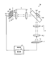
- FIG. 1 is a schematic diagram showing a schematic configuration of an optical property detection apparatus according to Embodiment 1 of the present invention.
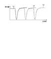
- FIG. 2 is a diagram schematically showing a detection result of the light receiving unit in the optical property detection apparatus according to Embodiment 1 of the present invention.
- FIG. 3 is a schematic diagram showing a schematic configuration of an optical characteristic detection device according to a modification of the first embodiment of the present invention.
- FIG. 4 is a diagram schematically showing a detection result of the light receiving unit in the optical characteristic detection device according to the modification of the first embodiment of the present invention.
- FIG. 5 is a schematic diagram showing a schematic configuration of an optical property detection apparatus according to Embodiment 2 of the present invention.
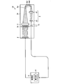
- FIG. 6 is a schematic diagram showing a schematic configuration of an optical characteristic detection apparatus according to Embodiment 3 of the present invention.
- FIG. 1 is a schematic diagram showing a schematic configuration of a refractive index detection apparatus according to Embodiment 1 of the present invention.
- a refractive index detection device that detects the refractive index of a test object will be described as an optical property detection device.
- the refractive index detection apparatus 1 shown in FIG. 1 has a light source unit 2 in which a plurality of light emitting points that emit light in different wavelength bands are arranged in a two-dimensional manner, and each of the plurality of light emitting points in the light source unit 2 is emitted.
- a first optical member 3 that collects light
- a polarizing member 4 that transmits a specific polarization component of light components emitted from the light source unit 2
- a detection unit 5 that has a detection surface that contacts the specimen SP
- a second optical member 6 that guides the light from the detection unit 5, a light receiving unit 7 that detects the amount of light received from the second optical member 6, and a control unit 8 that controls each part of the refractive index detection device 1; .
- the light source unit 2, the first optical member 3, the polarizing member 4, the detection unit 5, the second optical member 6, and the light receiving unit 7 function as an optical characteristic detection optical system.
- the light source unit 2 is configured by using a surface emitting laser array, and light sources 21 to 29 that emit light having different wavelength bands are arranged two-dimensionally.
- the light sources 21 to 29 emit light in a time division manner under the control of the control unit 8.
- the number of light sources of the light source unit 2 is nine.
- the present invention is not limited to this.
- the first optical member 3 condenses the light emitted from each of the light sources 21 to 29 of the light source unit 2 and causes the light to enter the detection unit 5.
- the first optical member 3 converts light emitted from each of the light sources 21 to 29 of the light source unit 2 into substantially parallel light, and enters the light through the collimating lens 31 that emits the substantially parallel light and the polarization member 4.
- a condensing lens 32 that focuses the light and forms an image on the detection surface 521 of the detection unit 5.
- the incident angle of the light emitted from each of the light sources 21 to 29 in the light source unit 2 to the detection surface 521 in the detection unit 5 is between the maximum angle and the minimum angle, and the refractive index and detection of the test object SP. It includes an angle that satisfies the plasmon resonance condition determined from the refractive index of the part 5, the material of the metal film 52, the film thickness, and the wavelength emitted from each of the light sources 21 to 29 in the light source part 2.
- the incident angle to the detection surface 521 includes 68 to 75 degrees between the maximum angle and the minimum angle.
- the incident angle on the detection surface 521 includes 67 to 76 degrees between the maximum angle and the minimum angle.
- the refractive index of the specimen SP is assumed to be 1.3 to 1.4, and more specifically 1.33 to 1.38.
- the refractive index of the detection unit 5 is 1.38 to 1.80, preferably 1.43 to 1.49.
- the wavelength emitted from each of the light sources 21 to 29 in the light source unit 2 is 405 nm to 2000 nm, preferably 1500 nm to 1600 nm.
- the polarizing member 4 is disposed on the optical path between the collimating lens 31 and the condenser lens 32.
- the polarization member 4 transmits a specific polarization component among the substantially parallel light components converted by the collimator lens 31.
- the polarizing member 4 is configured using a polarizing plate.
- the detection unit 5 is arranged so as to have different predetermined angles with respect to each of the first optical member 3 and the second optical member 6. Specifically, the detection unit 5 is arranged such that the optical axes of the first optical member 3 and the polarization member 4 and the surface on which light is incident or emitted in the detection unit 5 are approximately 45 degrees, and the second It arrange
- the detection unit 5 includes a prism 51 and a metal film 52 formed on the detection surface 521 in contact with the test object SP. As described above, the refractive index of the prism 51 is 1.38 to 1.80, preferably 1.43 to 1.49.
- the metal film 52 is configured by, for example, gold, silver and platinum alone or in combination.
- the thickness of the metal film 52 is 10 to 200 nm, preferably 10 to 50 nm, and more preferably 32 nm. In this case, the reflected light intensity due to resonance can be reduced to near zero.
- the detection surface 521 is disposed so as to be optically substantially conjugate with the light sources 21 to 29 of the light source unit 2.
- the metal film 52 is disposed at a substantially optical imaging position 522 formed by the first optical member 3 with each of the light sources 21 to 29 of the light source unit 2 as object planes.
- the second optical member 6 guides the light from the detection unit 5 to the light receiving unit 7.
- the second optical member 6 includes a collimator lens 61 and a condenser lens 62.
- the condenser lens 62 forms an image of the detection surface.
- the condenser lens 62 may not be provided, and collimated light may be incident on the light receiving unit 7.
- the light receiving unit 7 detects the amount of light received from the second optical member 6 and outputs the detection result to the control unit 8.
- the light receiving unit 7 is configured using a light receiving sensor having a two-dimensional light receiving element array such as a CCD (Charge Coupled Device) or a CMOS (Complementary Metal Oxide Semiconductor).
- the light receiving surface 7a of the light receiving unit 7 and the detection surface 521 of the detecting unit 5 are not in an optically conjugate positional relationship.
- the light receiving surface 7a is disposed behind the position where the conjugate image of the detection surface 521 is formed (image forming position by the condensing lens 62).
- the incident angle of the light beam on the detection surface 521 is related to the light incident position on the light receiving surface 7a.
- the control unit 8 is configured using a CPU (Central Processing Unit) or the like, and controls each unit of the refractive index detection apparatus 1.
- the control unit 8 includes a calculation unit 81 that calculates the refractive index of the test object SP based on the light intensity information input from the light receiving unit 7.
- the light sources 21 to 29 of the light source unit 2 have different wavelength bands under the control of the control unit 8 (for example, the light sources 21, 22, and 23). , Red light (620 nm to 750 nm), green light (495 nm to 570 nm) from the light sources 24, 25 and 26, and blue light (405 nm to 495 nm) from the light sources 27, 28 and 29 are sequentially emitted at different timings.
- the light emitted from the light source 21 of the light source unit 2 is converted into substantially parallel light by the collimator lens 31.
- the substantially parallel light converted by the collimator lens 31 enters the condenser lens 32 via the polarizing member 4.
- the light incident on the condenser lens 32 is condensed and forms an image on the detection surface 521 of the detection unit 5.
- the light incident on the detection unit 5 is reflected by the detection surface 521.
- the light reflected by the detection surface 521 of the detection unit 5 is guided to the light receiving unit 7 by the second optical member 6.
- the light guided by the second optical member 6 is detected by the light receiving unit 7. Further, light emitted from each of the light sources 22 to 29 of the light source unit 2 passes through the same optical path as the light emitted from the light source 21 described above, and is detected by the light receiving unit 7.
- FIG. 2 is a diagram schematically illustrating a detection result of the light receiving unit 7.
- the horizontal axis represents the incident angle
- the vertical axis represents the amount of received light.
- Curve L1 represents a resonance curve between the amount of received light having a red wavelength band and the incident angle
- curve L2 represents a resonance curve between the amount of received light having a green wavelength band and the incident angle
- curve L3. Shows a resonance curve between the amount of received light having a blue wavelength band and the incident angle.
- the refractive index detection apparatus 1 can acquire discrete wavelength information and continuous angle information. For this reason, the calculation unit 81 can detect the refractive index, optical dispersion, and the like of the test object SP based on the intensity information from the light receiving unit 7.
- the detection includes the light source unit 2 in which a plurality of light emitting points that emit light having different wavelength bands are arranged, and the detection surface 521 that contacts the test object SP.
- the first optical member 3 that focuses the light emitted from each of the light source 21, the light source 21 to the light source 29 and forms an image on the detection surface 521 of the detection unit 5, and the light from the detection surface 521 to the light receiving unit 7.
- the second optical member 6 that guides light, it is possible to reduce the size even when continuous incident angle information and discrete wavelength information are acquired.
- the incident position on the detection surface 521 of the detection unit 5 can be changed according to the positions of the light sources 21 to 29.
- the refractive index of the test object SP the refractive index of the detection unit 5, between the maximum angle and the minimum angle of the incident angle to the detection surface 521 in the detection unit 5, Since the angle includes the angle that satisfies the surface plasmon resonance condition determined from the material and film thickness of the metal film 52 and the wavelength of the light emitted from the light source unit 2, highly sensitive detection by surface plasmon resonance can be performed with a simple configuration.
- the refractive index is detected as the optical characteristic of the test object SP by surface plasmon resonance.
- the optical property of the test object SP is determined by the attenuated total reflection method. Detect as a characteristic.
- an optical property detection apparatus according to a modification of the first embodiment will be described.
- symbol is attached
- FIG. 3 is a schematic diagram showing a schematic configuration of an optical characteristic detection device according to a modification of the first embodiment of the present invention.
- an optical characteristic a refractive index detection apparatus that detects the refractive index of the test object SP will be described as an optical characteristic detection apparatus.
- the polarizing member 4 is deleted from the configuration of the refractive index detection device 1 according to Embodiment 1 described above.
- the detection unit 5a is arranged so as to have different predetermined angles with respect to each of the first optical member 3 and the second optical member 6. Specifically, the detection unit 5a is arranged such that the optical axis of the first optical member 3 and the surface on which light is incident or emitted from the detection unit 5a are approximately 45 degrees, and the second optical member 6 The optical axis and the surface on which light enters or exits in the detection unit 5a are arranged to be approximately 45 degrees.
- the detection unit 5a is configured using a prism.
- the refractive index of the detector 5a is 1.38 to 1.80, more preferably 1.43 to 1.49.
- the detection surface 5a1 is disposed so as to be optically substantially conjugate with the light sources 21 to 29 of the light source unit 2.
- the detection surface 5a1 of the detection unit 5a is disposed at a substantially optical imaging position 5a2 formed by the first optical member 3 with each of the light sources 21 to 29 of the light source unit 2 as object surfaces. Furthermore, the detection surface 5a1 of the detection unit 5a and the light reception surface 7a of the light reception unit 7 are not in an optically conjugate positional relationship.
- the light receiving surface 7a is disposed on the rear side of the position where the conjugate image of the detection surface 5a1 is formed.
- the incident angle of the light beam on the detection surface 5a1 is arranged in relation to the light beam incident position on the light receiving surface 7a.
- the light emitted from each of the light sources 21 to 29 in the light source unit 2 is condensed on the detection surface 5a1 by the condenser lens 32.
- the incident angle of the light emitted from each of the light sources 21 to 29 in the light source unit 2 to the detection surface 5a1 of the detection unit 5a (hereinafter simply referred to as “incident angle to the detection surface 5a1”) is the maximum angle and the minimum angle.
- the angle between the refractive index of the object SP and the refractive index of the detector 5a and the angle satisfying the total reflection condition determined from the wavelengths of the light emitted from each of the light sources 21 to 29 in the light source unit 2 is included.
- the incident angle to the detection surface 5a1 includes 68 degrees and 75 degrees, preferably 67 degrees and 76 degrees, between the maximum angle and the minimum angle.
- the refractive index detection device 1a configured in this manner sequentially emits light having different wavelength bands from each of the light sources 21 to 29 in the light source unit 2 at different timings under the control of the control unit 8.
- the light emitted from the light source 21 of the light source unit 2 is converted into substantially parallel light by the collimator lens 31.
- the substantially parallel light converted by the collimator lens 31 is condensed by the condenser lens 32 and imaged on the detection surface 5a1 of the detector 5a.
- the light condensed by the condenser lens 32 is reflected by the detection surface 5a1 of the detection unit 5a.
- the light reflected by the detection surface 5a1 of the detection unit 5a is guided by the second optical member 6.
- the light guided by the second optical member 6 is detected by the light receiving unit 7. Further, light emitted from each of the light sources 22 to 29 of the light source unit 2 passes through the same optical path as the light emitted from the light source 21 described above, and is detected by the light receiving unit 7.
- FIG. 4 is a diagram schematically showing the detection result of the light receiving unit 7.
- the horizontal axis indicates the incident angle
- the vertical axis indicates the amount of received light.
- Curve L11 shows the relationship between the amount of received light having the red wavelength band and the incident angle
- curve L12 shows the relationship between the amount of received light having the green wavelength band and the incident angle
- curve L13 shows the blue color. The relationship between the amount of light received in the wavelength band and the incident angle is shown.
- the refractive index detection device 1a can acquire discrete wavelength information and continuous angle information. For this reason, the calculation unit 81 can detect the refractive index, optical dispersion, and the like of the test object SP based on the intensity information from the light receiving unit 7.
- the refractive index of the test object SP the refractive index of the detection unit 5a, and the refractive index between the maximum angle and the minimum angle of the incident angle on the detection surface 5a1. Since the angle that satisfies the total reflection condition determined from the wavelength of the light emitted from the light source unit 2 is included, even when continuous incident angle information and discrete wavelength information are acquired by the total reflection critical method, the size can be reduced. Can be achieved.
- the incident position on the detection surface 5a1 of the detection unit 5a can be changed according to the position of each of the light sources 21 to 29.
- FIG. 5 is a schematic diagram showing a schematic configuration of an optical property detection apparatus according to Embodiment 2 of the present invention.
- an optical characteristic a refractive index detection apparatus that detects the refractive index of the test object SP will be described as an optical characteristic detection apparatus.
- the light source unit 2 b includes a light source 201 and a light emitting member 202.
- the light source 201 emits light having different predetermined wavelengths to each of a plurality of optical fibers constituting a light emitting member 202 described later.
- the light source 201 is configured using a plurality of light sources (semiconductor lasers) such as a laser light source.
- the light emitting member 202 is configured using a plurality of optical fibers. In the second embodiment, the light emitting member 202 is configured using two or more optical fibers. Specifically, the light emitting member 202 includes a first irradiation fiber 21b to a ninth irradiation fiber 29b. Each of the first irradiation fiber 21b to the ninth irradiation fiber 29b receives light having different wavelength bands emitted from the light source 201 and emits the light from the emission end 202b. Further, the emission end 202b of each of the first irradiation fiber 21b to the ninth irradiation fiber 29b and the detection surface 521 of the detection unit 5 are in an optically conjugate positional relationship.
- the light source 201 emits light having different wavelength bands under the control of the control unit 8.
- the light emitted from the light source 201 is emitted from the emission end 202b of the first irradiation fiber 21b.
- the light emitted from the emission end 202b of the first irradiation fiber 21b is converted into substantially parallel light by the collimator lens 31.
- the substantially parallel light converted by the collimator lens 31 enters the condenser lens 32 via the polarizing member 4.
- the light incident on the condenser lens 32 is condensed and forms an image on the detection surface 521 of the detection unit 5.
- the light incident on the detection unit 5 is reflected by the detection surface 521 of the detection unit 5.
- the light reflected by the detection surface 521 of the detection unit 5 enters the light receiving unit 7 through the second optical member 6.
- the light emitted from each of the second irradiation fiber 22b to the ninth irradiation fiber 29b passes through the same optical path as the light emitted from the first irradiation fiber 21b described above, and is detected by the light receiving unit 7.
- the light source unit 2b is configured by using the light source 201 and the first irradiation fiber 21b to the ninth irradiation fiber 29b, thereby making it possible to narrow the vicinity of the emission end of the light source unit 2b. Diameter can be achieved.
- the incident position on the detection surface 521 of the detection unit 5 can be changed according to the position of each of the first irradiation fiber 21b to the ninth irradiation fiber 29b.
- the metal film 52 is not used, and the refraction of the test object SP is performed when the incident angles of the plurality of lights on the detection surface 521 of the detection unit 5 are between the maximum angle and the minimum angle. And an angle that satisfies the total reflection condition determined from the wavelength emitted from each of the first irradiating fiber 21b to the ninth irradiating fiber 29b can be easily detected by the attenuated total reflection method. It can be performed.
- FIG. 6 is a schematic diagram showing a schematic configuration of an optical characteristic detection apparatus according to Embodiment 3 of the present invention.
- an optical characteristic a refractive index detection apparatus that detects the refractive index of the test object SP will be described as an optical characteristic apparatus.
- the measurement probe 70 includes a light source unit 2, a first optical member 3d, a polarizing member 4, a detection unit 5d, a second optical member 6, and a light receiving unit 7.
- 1st optical member 3d is comprised using a condensing lens.
- the first optical member 3d collects light emitted from each of the light sources 21 to 29 of the light source unit 2 and having different wavelength bands.
- the detection unit 5d is configured using a prism having a substantially trapezoidal cross section.
- the detection unit 5d has a detection surface 5d1 that comes into contact with the test object.
- a metal film 5d2 is formed on the detection surface 5d1.
- the detection surface 5d1 is disposed at an optically substantially conjugate position with the light sources 21 to 29 of the light source unit 2.
- the detection unit 5 d reflects the light emitted from the first optical member 3 d toward the second optical member 6.
- the light receiving unit 7 is disposed at a position behind the imaging position by the second optical member 6 so that the incident angle of the light beam on the detection surface 5d1 is related to the light beam incident position on the light receiving surface 7a. .
- the light source unit 2 sequentially emits light having different wavelength bands at different timings under the control of the control unit 8.
- the light emitted from the light source 21 of the light source unit 2 is collected by the first optical member 3d.
- the light condensed by the first optical member 3d enters the detection unit 5d via the polarizing member 4.
- the light incident on the detection unit 5d is reflected by the detection surface 5d1.
- the amount of light reflected by the detection surface 5 d 1 of the detection unit 5 d is guided by the second optical member 6 and detected by the light receiving unit 7.
- light emitted from each of the light sources 22 to 29 of the light source unit 2 passes through the same optical path as the light emitted from the light source 21 described above, and is detected by the light receiving unit 7.
- the present invention is not limited to the above-described embodiments and modifications as they are, and in the implementation stage, the constituent elements can be modified and embodied without departing from the spirit of the invention.
- Various inventions can be formed by appropriately combining a plurality of constituent elements disclosed in the above-described embodiments. For example, some constituent elements may be deleted from all the constituent elements described in the above-described embodiments and modifications. Furthermore, you may combine suitably the component demonstrated by each embodiment and the modification.
Landscapes
- Physics & Mathematics (AREA)
- Health & Medical Sciences (AREA)
- Life Sciences & Earth Sciences (AREA)
- Chemical & Material Sciences (AREA)
- Analytical Chemistry (AREA)
- Biochemistry (AREA)
- General Health & Medical Sciences (AREA)
- General Physics & Mathematics (AREA)
- Immunology (AREA)
- Pathology (AREA)
- Investigating Or Analysing Materials By Optical Means (AREA)
Abstract
入射角度情報および波長情報を同時に取得する場合であっても、小型化を図ることができる光学特性検出光学系、測定プローブおよび光学特性検出装置を提供する。光学特性検出光学系は、互いに異なる波長帯域を有する光を出射する複数の発光点が配列された光源部2と、所定の屈折率を有する部材を用いて形成され、被検物と接触する検出面521を有する検出部5と、複数の光源21~光源29の各々から出射された光を集光して検出面521に結像する第1光学部材3と、検出面521からの光を受光可能な受光部7と、検出面521からの光を受光部7へ導光する第2光学部材6と、を備える。
Description
本発明は、生体等の被検物の屈折率を検出する際に用いる光学特性検出光学系、該光学特性検出光学系を備えた測定プローブおよび光学特性検出装置に関する。
従来、減衰全反射(Attenuated Total Reflection)法または表面プラズモン共鳴(Surface Plasmon Resonance)法等を用いて被検物の屈折率を取得し、この取得した屈折率に基づいて、被検物の特性を分析する装置が知られている。減衰全反射法または表面プラズモン共鳴法では、通常、被検物の被検面への光の入射角度情報を取得し、取得した入射角度情報に基づいて、全反射臨界角またはプラズモン共鳴角を算出する算出方法、および波長情報を取得し、取得した波長情報に基づいて全反射臨界角またはプラズモン共鳴角を算出する算出方法のどちらか一方を用いて被検物の光学特性の分析を行う。つまり、減衰全反射法または表面プラズモン共鳴法では、入射角度情報および波長情報のどちらか一方を取得する方法が一般的である。
また、特許文献1には、入射角度情報および波長情報を同時に取得することで、被検物の特性を分析する技術が記載されている。この技術では、白色光源と、底面に被検物を貼付したプリズムと、プリズムから反射された反射光の角度広がり方向と平行に配置された分光スリット、分光器と、二次元光検出器と、を設け、入射角度情報および波長情報を同時に示す二次元画像を取得することによって、被検物の特性を分析する。
しかしながら、上述した従来技術のうち、入射角度情報に基づいて全反射臨界角またはプラズモン共鳴角を算出する算出方法では、検出に用いる検出面でのエバネッセント波の浸み出し深さが波長に大きく依存するため、入射角度情報のみを取得する場合、単波長での測定において様々な大きさの被検物に対応することができないという問題点があった。
また、上述した従来技術のうち、波長情報に基づいて全反射臨界角またはプラズモン共鳴角を算出する算出方法では、分光器および高輝度の白色光源が必要であり、装置が大型化するという問題点があった。
さらに、上述した特許文献1では、波長情報を取得するため、分光器および高輝度の白色光源が必要であり、装置が大型化するという問題点があった。
本発明は、上記に鑑みてなされたものであって、入射角度情報および波長情報を同時に取得する場合であっても、小型化を図ることができる光学特性検出光学系、測定プローブおよび光学特性検出装置を提供することを目的とする。
上述した課題を解決し、目的を達成するために、本発明に係る光学特性検出光学系は、互いに異なる波長帯域を有する光を出射する複数の発光点が配列された光源部と、所定の屈折率を有する部材を用いて形成され、被検物と接触する検出面を有する検出部と、前記複数の発光点の各々から出射された光を前記検出面に集光する第1光学部材と、前記検出面からの光を受光可能な受光部と、前記検出面からの光を前記受光部へ導光する第2光学部材と、を備えたことを特徴とする。
また、本発明に係る光学特性検出光学系は、上記発明において、前記検出部は、前記検出面に金属膜が成膜されていることを特徴とする。
また、本発明に係る光学特性検出光学系は、上記発明において、前記複数の発光点の各々から出射された光の前記検出面への入射角は、その最大角と最小角との間に、前記被検物の屈折率、前記検出部の屈折率、前記金属膜の材質、膜厚および前記複数の発光点の各々が出射する波長から定まるプラズモン共鳴条件を満たす角度を含むことを特徴とする。
また、本発明に係る光学特性検出光学系は、上記発明において、前記複数の発光点の各々から出射された光の前記検出面への入射角は、その最大角と最小角との間に、前記被検物の屈折率、前記検出部の屈折率および前記複数の発光点の各々が出射する波長から定まる全反射条件に満たす角度を含むことを特徴とする。
また、本発明に係る光学特性検出光学系は、上記発明において、前記複数の発光点の各々および前記検出面は、光学的に共役な位置関係にあることを特徴とする。
また、本発明に係る光学特性検出光学系は、上記発明において、前記光源部は、前記複数の発光点が二次元的に配列された面発光レーザアレイを有することを特徴とする。
また、本発明に係る光学特性検出光学系は、上記発明において、前記光源部は、互いに異なる波長帯域の光を出射する複数の光源と、前記複数の光源の各々が出射した光を一方の端部で受光し、この受光した光を伝播して他方の端部から出射する複数の照射ファイバと、を有することを特徴とする。
また、本発明に係る測定プローブは、上述した光学特性光学系を備えた、前記検出面が前記被検物に接触可能であることを特徴とする。
また、本発明に係る光学特性検出装置は、上述した光学特性検出光学系と、前記受光部によって受光した前記光の強度情報に基づいて、前記被検物の屈折率を算出する算出部と、を備えたことを特徴とする。
本発明によれば、入射角度情報および波長情報を同時に取得する場合であっても、小型化を図ることができるという効果を奏する。
以下、本発明を実施するための形態を図面とともに詳細に説明する。なお、以下の実施の形態により本発明が限定されるものではない。また、以下の説明において参照する各図は、本発明の内容を理解でき得る程度に形状、大きさ、および位置関係を概略的に示してあるに過ぎない。即ち、本発明は、各図で例示された形状、大きさ、および位置関係のみに限定されるものではない。また、同一の構成には同一の符号を付して説明する。
(実施の形態1)
〔屈折率検出装置の構成〕
図1は、本発明の実施の形態1に係る屈折率検出装置の概略構成を示す模式図である。ここでは、光学特性として、被検物の屈折率の検出を行う屈折率検出装置を光学特性検出装置として説明する。
〔屈折率検出装置の構成〕
図1は、本発明の実施の形態1に係る屈折率検出装置の概略構成を示す模式図である。ここでは、光学特性として、被検物の屈折率の検出を行う屈折率検出装置を光学特性検出装置として説明する。
図1に示す屈折率検出装置1は、互いに異なる波長帯域の光を出射する複数の発光点が二次元状に配列された光源部2と、光源部2における複数の発光点の各々が出射した光を集光する第1光学部材3と、光源部2が出射した光の成分のうち特定偏光成分を透過する偏光部材4と、被検物SPと接触する検出面を有する検出部5と、検出部5からの光を導光する第2光学部材6と、第2光学部材6からの光の受光量を検出する受光部7と、屈折率検出装置1の各部を制御する制御部8と、を備える。本実施の形態1では、光源部2、第1光学部材3、偏光部材4、検出部5、第2光学部材6および受光部7が光学特性検出光学系として機能する。
光源部2は、面発光レーザアレイを用いて構成され、互いに異なる波長帯域の光を出射する光源21~光源29が二次元状に配列される。光源部2は、制御部8の制御のもと、光源21~光源29が時分割で光を出射する。なお、本実施の形態1では、光源部2の光源が9個であるが、これに限定されるわけでなく、複数、例えば2個以上あればよい。
第1光学部材3は、光源部2の光源21~光源29の各々が出射した光を集光して検出部5へ入射させる。第1光学部材3は、光源部2の光源21~光源29の各々が出射した光を略平行光に変換し、この略平行光を出射するコリメートレンズ31と、偏光部材4を介して入射した光を集光して検出部5の検出面521へ結像する集光レンズ32と、を有する。光源部2における光源21~光源29の各々から出射された光の検出部5における検出面521への入射角は、その最大角と最小角との間に、被検物SPの屈折率、検出部5の屈折率、金属膜52の材質、膜厚および光源部2における光源21~光源29の各々が出射する波長から定まるプラズモン共鳴条件を満たす角度を含む。
ここで、検出面521への入射角は、その最大角と最小角との間に、68度~75度を含む。好ましくは、測定の誤差や測定光学系の物作り上の公差を考慮した場合、検出面521への入射角は、その最大角と最小角との間に、67度~76度を含む。また、被検物SPの屈折率としては、1.3~1.4が想定され、より具体的には1.33~1.38が想定される。また、検出部5の屈折率は、1.38~1.80、好ましくは1.43~1.49である。さらに、光源部2における光源21~光源29の各々が出射する波長は、405nm~2000nm、好ましくは1500nm~1600nmである。
偏光部材4は、コリメートレンズ31と集光レンズ32との光路上に配置される。偏光部材4は、コリメートレンズ31が変換した略平行光の成分のうち特定偏光成分を透過する。偏光部材4は、偏光板を用いて構成される。
検出部5は、第1光学部材3および第2光学部材6の各々に対して互いに異なる所定の角度となるように配置される。具体的には、検出部5は、第1光学部材3および偏光部材4の光軸と検出部5において光が入射または出射する面とが略45度となるように配置されるとともに、第2光学部材6の光軸と検出部5において光が入射または出射する面とが略45度となるように配置される。検出部5は、プリズム51と、被検物SPと接触する検出面521に成膜された金属膜52と、を有する。プリズム51の屈折率は、前述の通り、1.38~1.80、好ましくは1.43~1.49である。金属膜52は、例えば金、銀および白金を単独または組み合わせて構成される。金属膜52の厚さは、10~200nm、好ましくは10~50nmであり、より好ましくは32nmである。この場合、共鳴による反射光強度を0付近まで落とすことができる。また、検出面521は、光源部2の光源21~光源29と光学的に略共役関係に位置するように配置される。金属膜52は、光源部2の光源21~光源29の各々を物体面として、第1光学部材3によって形成される光学的な略結像位置522に配置される。
第2光学部材6は、検出部5からの光を受光部7へ導光する。第2光学部材6は、コリメートレンズ61と、集光レンズ62と、を有する。集光レンズ62は検出面の像を結像する。集光レンズ62はなくてもよく、受光部7へコリメート光を入射してもよい。
受光部7は、第2光学部材6からの光の受光量を検出し、この検出結果を制御部8へ出力する。受光部7は、CCD(Charge Coupled Device)またはCMOS(Complementary Metal Oxide Semiconductor)等の2次元的な受光素子列を持つ受光センサを用いて構成される。受光部7の受光面7aおよび検出部5の検出面521は、光学的に共役な位置関係とはしていない。受光面7aは検出面521の共役像が形成される位置(集光レンズ62による結像位置)よりも後側に配置されている。検出面521への光線の入射角が、受光面7aへの光線入射位置に関係する配置としている。
制御部8は、CPU(Central Processing Unit)等を用いて構成され、屈折率検出装置1の各部を制御する。制御部8は、受光部7から入力された光の強度情報に基づいて、被検物SPの屈折率を算出する算出部81を有する。
このように構成された屈折率検出装置1は、制御部8の制御のもと、光源部2の光源21~光源29の各々が互いに異なる波長帯域を有する光(例えば、光源21、22、23にて赤色光(620nm~750nm)、光源24、25、26にて緑色光(495nm~570nm)、光源27、28、29にて青色光(405nm~495nm))を異なるタイミングで順次出射する。光源部2の光源21から出射された光は、コリメートレンズ31によって略平行光に変換される。コリメートレンズ31によって変換された略平行光は、偏光部材4を介して集光レンズ32に入射する。集光レンズ32に入射した光は、集光されて検出部5の検出面521に結像する。検出部5に入射した光は、検出面521で反射する。検出部5の検出面521で反射した光は、第2光学部材6によって受光部7に導光される。第2光学部材6によって導光された光は、受光部7によって検出される。また、光源部2の光源22~光源29の各々から発せられた光は、上述した光源21から発せられた光と同様の光路を通り、受光部7によって検出される。
次に、受光部7が受光する受光量について説明する。図2は、受光部7の検出結果を模式的に示す図である。図2において、横軸が入射角を示し、縦軸が受光量を示す。また、曲線L1が赤色の波長帯域を有する光の受光量と入射角との共鳴曲線を示し、曲線L2が緑色の波長帯域を有する光の受光量と入射角との共鳴曲線を示し、曲線L3が青色の波長帯域を有する光の受光量と入射角との共鳴曲線を示す。
図2の曲線L1~曲線L3に示すように、屈折率検出装置1は、離散的な波長情報および連続的な角度情報を取得することができる。このため、算出部81は、受光部7からの強度情報に基づいて、被検物SPの屈折率や光学的な分散等を検出することができる。
以上説明した本発明の実施の形態1によれば、互いに異なる波長帯域を有する光を出射する複数の発光点が配列された光源部2と、被検物SPと接触する検出面521を有する検出部5と、光源21~光源29の各々から出射された光を集光して検出部5の検出面521へ結像する第1光学部材3と、検出面521からの光を受光部7へ導光する第2光学部材6と、を設けることによって、連続的な入射角度情報および離散的な波長情報を取得する場合であっても、小型化を図ることができる。
また、本発明の実施の形態1によれば、光源21~光源29の各々の位置によって検出部5の検出面521への入射位置を変更することができる。
また、本発明の実施の形態1によれば、検出部5における検出面521への入射角における最大角と最小角との間に、被検物SPの屈折率、検出部5の屈折率、金属膜52の材質と膜厚、および光源部2が出射する光の波長から定まる表面プラズモン共鳴条件を満たす角度を含むので、表面プラズモン共鳴による高感度な検出を単純な構成で行うことができる。
(実施の形態1の変形例)
次に、本発明の実施の形態1の変形例について説明する。上述した実施の形態1では、表面プラズモン共鳴によって被検物SPの光学特性として屈折率を検出していたが、本実施の形態1の変形例では、減衰全反射法によって被検物SPの光学特性として検出する。以下においては、本実施の形態1の変形例に係る光学特性検出装置について説明する。なお、上述した実施の形態1に係る屈折率検出装置1と同一の構成には同一の符号を付して説明を省略する。
次に、本発明の実施の形態1の変形例について説明する。上述した実施の形態1では、表面プラズモン共鳴によって被検物SPの光学特性として屈折率を検出していたが、本実施の形態1の変形例では、減衰全反射法によって被検物SPの光学特性として検出する。以下においては、本実施の形態1の変形例に係る光学特性検出装置について説明する。なお、上述した実施の形態1に係る屈折率検出装置1と同一の構成には同一の符号を付して説明を省略する。
〔屈折率検出装置の構成〕
図3は、本発明の実施の形態1の変形例に係る光学特性検出装置の概略構成を示す模式図である。ここでも、光学特性として、被検物SPの屈折率の検出を行う屈折率検出装置を光学特性検出装置として説明する。
図3は、本発明の実施の形態1の変形例に係る光学特性検出装置の概略構成を示す模式図である。ここでも、光学特性として、被検物SPの屈折率の検出を行う屈折率検出装置を光学特性検出装置として説明する。
図3に示す屈折率検出装置1aは、上述した実施の形態1に係る屈折率検出装置1の検出部5に換えて、検出部5aを備える。さらに、図3に示す屈折率検出装置1aは、上述した実施の形態1に係る屈折率検出装置1の構成から偏光部材4を削除した。
検出部5aは、第1光学部材3および第2光学部材6の各々に対して互いに異なる所定の角度となるように配置される。具体的には、検出部5aは、第1光学部材3の光軸と検出部5aにおいて光が入射または出射する面とが略45度となるように配置されるとともに、第2光学部材6の光軸と検出部5aにおいて光が入射または出射する面とが略45度となるように配置される。検出部5aは、プリズムを用いて構成される。検出部5aの屈折率は、1.38~1.80、より好ましくは1.43~1.49である。また、検出面5a1は、光源部2の光源21~光源29と光学的に略共役関係に位置するように配置される。検出部5aの検出面5a1は、光源部2の光源21~光源29の各々を物体面として、第1光学部材3によって形成される光学的な略結像位置5a2に配置される。さらに、検出部5aの検出面5a1および受光部7の受光面7aは、光学的に共役な位置関係とはしていない。受光面7aは検出面5a1の共役像が形成される位置よりも後側に配置されている。検出面5a1への光線の入射角が、受光面7aへの光線入射位置に関係する配置としている。さらにまた、検出部5aは、光源部2における光源21~光源29の各々から出射された光が集光レンズ32によって検出面5a1に集光される。光源部2における光源21~光源29の各々が出射した光の検出部5aの検出面5a1への入射角(以下、単に「検出面5a1への入射角」という)は、その最大角と最小角との間に、被検物SPの屈折率および検出部5aの屈折率、光源部2における光源21~光源29の各々が出射する光の波長から定まる全反射条件を満たす角度を含む。
ここで、検出面5a1への入射角は、その最大角と最小角との間に、68度と75度を含み、好ましくは67度と76度を含む。
このように構成された屈折率検出装置1aは、制御部8の制御のもと、光源部2における光源21~光源29の各々が互いに異なる波長帯域を有する光を異なるタイミングで順次出射する。光源部2の光源21から出射された光は、コリメートレンズ31によって略平行光に変換される。コリメートレンズ31によって変換された略平行光は、集光レンズ32によって集光されて検出部5aの検出面5a1に結像される。集光レンズ32によって集光された光は、検出部5aの検出面5a1で反射する。検出部5aの検出面5a1で反射した光は、第2光学部材6によって導光される。第2光学部材6によって導光された光は、受光部7によって検出される。また、光源部2の光源22~光源29の各々から発せられた光は、上述した光源21から発せられた光と同様の光路を通り、受光部7によって検出される。
次に、受光部7が受光する受光量について説明する。図4は、受光部7の検出結果を模式的に示す図である。図4において、横軸が入射角を示し、縦軸が受光量を示す。また、曲線L11が赤色の波長帯域を有する光の受光量と入射角との関係を示し、曲線L12が緑色の波長帯域を有する光の受光量と入射角との関係を示し、曲線L13が青色の波長帯域を有する光の受光量と入射角との関係を示す。
図4の曲線L11~曲線L13に示すように、屈折率検出装置1aは、離散的な波長情報および連続的な角度情報を取得することができる。このため、算出部81は、受光部7からの強度情報に基づいて、被検物SPの屈折率や光学的な分散等を検出することができる。
以上説明した本発明の実施の形態1の変形例によれば、検出面5a1への入射角における最大角と最小角との間に、被検物SPの屈折率、検出部5aの屈折率および光源部2が出射する光の波長から定まる全反射条件を満たす角度を含むので、全反射臨界法によって、連続的な入射角度情報および離散的な波長情報を取得する場合であっても、小型化を図ることができる。
また、本発明の実施の形態1の変形例によれば、光源21~光源29の各々の位置によって検出部5aの検出面5a1への入射位置を変更することができる。
(実施の形態2)
次に、本発明の実施の形態2について説明する。上述した実施の形態1では、光源部2として面発光レーザアレイを用いていたが、本実施の形態2では、複数の照射ファイバを介して互いに異なる波長帯域を有する光を出射する。以下においては、本実施の形態2に係る光学特性検出装置の構成について説明する。なお、上述した実施の形態1に係る屈折率検出装置1と同一の構成には同一の符号を付して説明を省略する。
次に、本発明の実施の形態2について説明する。上述した実施の形態1では、光源部2として面発光レーザアレイを用いていたが、本実施の形態2では、複数の照射ファイバを介して互いに異なる波長帯域を有する光を出射する。以下においては、本実施の形態2に係る光学特性検出装置の構成について説明する。なお、上述した実施の形態1に係る屈折率検出装置1と同一の構成には同一の符号を付して説明を省略する。
〔屈折率検出装置の構成〕
図5は、本発明の実施の形態2に係る光学特性検出装置の概略構成を示す模式図である。ここでも、光学特性として、被検物SPの屈折率の検出を行う屈折率検出装置を光学特性検出装置として説明する。
図5は、本発明の実施の形態2に係る光学特性検出装置の概略構成を示す模式図である。ここでも、光学特性として、被検物SPの屈折率の検出を行う屈折率検出装置を光学特性検出装置として説明する。
図5に示す屈折率検出装置1bは、上述した実施の形態1に係る屈折率検出装置1の光源部2に換えて、光源部2bを備える。光源部2bは、光源201と、発光部材202と、を有する。
光源201は、後述する発光部材202を構成する複数の光ファイバの各々に互いに異なる所定波長を有する光を出射する。光源201は、レーザ光源等の複数の光源(半導体レーザ)を用いて構成される。
発光部材202は、複数の光ファイバを用いて構成される。本実施の形態2では、発光部材202は、2本以上の光ファイバを用いて構成される。具体的には、発光部材202は、第1照射ファイバ21b~第9照射ファイバ29bを有する。第1照射ファイバ21b~第9照射ファイバ29bの各々は、光源201から出射された互いに異なる波長帯域を有する光が入射され、この光を出射端202bから出射する。また、第1照射ファイバ21b~第9照射ファイバ29bの各々の出射端202bおよび検出部5の検出面521は、光学的に共役な位置関係にある。
このように構成された屈折率検出装置1bは、制御部8の制御のもと、光源201が互いに異なる波長帯域を有する光を出射する。光源201から出射された光は、第1照射ファイバ21bの出射端202bから出射される。第1照射ファイバ21bの出射端202bから出射された光は、コリメートレンズ31によって略平行光に変換される。コリメートレンズ31によって変換された略平行光は、偏光部材4を介して集光レンズ32に入射する。集光レンズ32に入射した光は、集光されて検出部5の検出面521に結像する。検出部5に入射した光は、検出部5の検出面521で反射する。検出部5の検出面521で反射した光は、第2光学部材6を介して受光部7へ入射する。また、第2照射ファイバ22b~第9照射ファイバ29bの各々から出射された光は、上述した第1照射ファイバ21bから出射された光と同様の光路を通り、受光部7によって検出される。
以上説明した本発明の実施の形態2によれば、光源部2bを光源201と第1照射ファイバ21b~第9照射ファイバ29bとを用いて構成することによって、光源部2bの射出端近傍の細径化を図ることができる。
また、本発明の実施の形態2によれば、第1照射ファイバ21b~第9照射ファイバ29bの各々の位置によって検出部5の検出面521への入射位置を変更することができる。
また、本発明の実施の形態2では、金属膜52を用いず、検出部5の検出面521における複数の光の入射角がその最大角と最小角との間に、被検物SPの屈折率、検出部5の屈折率および第1照射ファイバ21b~第9照射ファイバ29bの各々が出射する波長から定まる全反射条件を満たす角度を含むように構成すれば、減衰全反射法による簡易な検出を行うことができる。
(実施の形態3)
次に、本発明の実施の形態3について説明する。上述した実施の形態1では、第1光学部材3の光軸と第2光学部材6の光軸とがなす角度が略直角となるように配置されていたが、本実施の形態3では、第1光学部材の光軸と第2光学部材の光軸とが略平行に配置される。以下においては、本実施の形態3に係る光学特性検出装置について説明する。なお、上述した実施の形態1に係る屈折率検出装置1と同一の構成には同一の符号を付して説明を省略する。
次に、本発明の実施の形態3について説明する。上述した実施の形態1では、第1光学部材3の光軸と第2光学部材6の光軸とがなす角度が略直角となるように配置されていたが、本実施の形態3では、第1光学部材の光軸と第2光学部材の光軸とが略平行に配置される。以下においては、本実施の形態3に係る光学特性検出装置について説明する。なお、上述した実施の形態1に係る屈折率検出装置1と同一の構成には同一の符号を付して説明を省略する。
〔屈折率検出装置の構成〕
図6は、本発明の実施の形態3に係る光学特性検出装置の概略構成を示す模式図である。ここでも、光学特性として、被検物SPの屈折率の検出を行う屈折率検出装置を光学特性装置として説明する。
図6は、本発明の実施の形態3に係る光学特性検出装置の概略構成を示す模式図である。ここでも、光学特性として、被検物SPの屈折率の検出を行う屈折率検出装置を光学特性装置として説明する。
図6に示す屈折率検出装置1dは、測定プローブ70と、制御部8と、を備える。
測定プローブ70は、光源部2と、第1光学部材3dと、偏光部材4と、検出部5dと、第2光学部材6と、受光部7と、を備える。
第1光学部材3dは、集光レンズを用いて構成される。第1光学部材3dは、光源部2の光源21~光源29の各々から出射された互いに波長帯域が異なる光を集光する。
検出部5dは、断面が略台形をなすプリズムを用いて構成される。検出部5dは、被検物と接触する検出面5d1を有する。また、検出面5d1には、金属膜5d2が成膜される。さらに、検出面5d1は、光源部2の光源21~29と光学的な略共役位置に配置される。検出部5dは、第1光学部材3dから出射された光を第2光学部材6に向けて反射する。
受光部7は、検出面5d1への光線の入射角が、受光面7aへの光線入射位置に関係するように、第2光学部材6による結像位置よりも後側の位置に配置している。
このように構成された屈折率検出装置1dは、制御部8の制御のもと、光源部2が互いに異なる波長帯域を有する光を異なるタイミングで順次出射する。光源部2の光源21から出射された光は、第1光学部材3dによって集光される。第1光学部材3dによって集光された光は、偏光部材4を介して検出部5dに入射する。検出部5dに入射した光は、検出面5d1で反射する。検出部5dの検出面5d1で反射した光の光量は、第2光学部材6によって導光され、受光部7によって検出される。また、光源部2の光源22~光源29の各々から出射された光は、上述した光源21から発せられた光と同様の光路を通り、受光部7によって検出される。
以上説明した本発明の実施の形態4によれば、入射角度情報および波長情報を同時に取得する場合であっても、小型化を図ることができる。
本発明は、上述した実施の形態および変形例そのままに限定されるものではなく、実施段階では、発明の要旨を逸脱しない範囲内で構成要素を変形して具体化することができる。また、上述した実施の形態に開示されている複数の構成要素を適宜組み合わせることによって、種々の発明を形成することができる。例えば、上述した実施の形態および変形例に記載した全構成要素からいくつかの構成要素を削除してもよい。さらに、各実施の形態および変形例で説明した構成要素を適宜組み合わせてもよい。
また、明細書または図面において、少なくとも一度、より広義または同義な異なる用語とともに記載された用語は、明細書または図面のいかなる箇所においても、その異なる用語に置き換えることができる。このように、発明の主旨を逸脱しない範囲内において種々の変形や応用が可能である。
1,1a,1b,1d 屈折率検出装置
2,2b 光源部
3,3d 第1光学部材
4 偏光部材
5,5a、5d 検出部
5a1,5d1,521 検出面
5a2,522 結像位置
5d2,52 金属膜
6 第2光学部材
7 受光部
7a 受光面
8 制御部
21~29, 光源
21b 第1照射ファイバ
22b 第2照射ファイバ
23b 第3照射ファイバ
24b 第4照射ファイバ
25b 第5照射ファイバ
26b 第6照射ファイバ
27b 第7照射ファイバ
28b 第8照射ファイバ
29b 第9照射ファイバ
31,61 コリメートレンズ
32,62 集光レンズ
51 プリズム
70 測定プローブ
81 算出部
202 発光部材
202b 出射端
SP 被検物
2,2b 光源部
3,3d 第1光学部材
4 偏光部材
5,5a、5d 検出部
5a1,5d1,521 検出面
5a2,522 結像位置
5d2,52 金属膜
6 第2光学部材
7 受光部
7a 受光面
8 制御部
21~29, 光源
21b 第1照射ファイバ
22b 第2照射ファイバ
23b 第3照射ファイバ
24b 第4照射ファイバ
25b 第5照射ファイバ
26b 第6照射ファイバ
27b 第7照射ファイバ
28b 第8照射ファイバ
29b 第9照射ファイバ
31,61 コリメートレンズ
32,62 集光レンズ
51 プリズム
70 測定プローブ
81 算出部
202 発光部材
202b 出射端
SP 被検物
Claims (9)
- 互いに異なる波長帯域を有する光を出射する複数の発光点が配列された光源部と、
所定の屈折率を有する部材を用いて形成され、被検物と接触する検出面を有する検出部と、
前記複数の発光点の各々から出射された光を集光して前記検出面に結像する第1光学部材と、
前記検出面からの光を受光可能な受光部と、
前記検出面からの光を前記受光部へ導光する第2光学部材と、
を備えたことを特徴とする光学特性検出光学系。 - 前記検出部は、前記検出面に金属膜が成膜されていることを特徴とする請求項1に記載の光学特性検出光学系。
- 前記複数の発光点の各々から出射された光の前記検出面への入射角は、その最大角と最小角との間に、前記被検物の屈折率、前記検出部の屈折率、前記金属膜の材質、膜厚および前記複数の発光点の各々が出射する波長から定まるプラズモン共鳴条件を満たす角度を含むことを特徴とする請求項2に記載の光学特性検出光学系。
- 前記複数の発光点の各々から出射された光の前記検出面への入射角は、その最大角と最小角との間に、前記被検物の屈折率、前記検出部の屈折率および前記複数の発光点の各々が出射する波長から定まる全反射条件に満たす角度を含むことを特徴とする請求項1に記載の光学特性検出光学系。
- 前記複数の発光点の各々および前記検出面は、光学的に共役な位置関係にあることを特徴とする請求項1~4のいずれか一つに記載の光学特性検出光学系。
- 前記光源部は、前記複数の発光点が二次元状に配列された面発光レーザアレイを有することを特徴とする請求項1~5のいずれか一つに記載の光学特性検出光学系。
- 前記光源部は、
互いに異なる波長帯域の光を出射する複数の光源と、
前記複数の光源の各々が出射した光を一方の端部で受光し、この受光した光を伝播して他方の端部から出射する複数の照射ファイバと、
を有することを特徴とする請求項1~5のいずれか一つに記載の光学特性検出光学系。 - 請求項1~7のいずれか一つに記載の光学特性検出光学系を備え、前記検出面が前記被検物に接触可能であることを特徴とする測定プローブ。
- 請求項1~7のいずれか一つに記載の光学特性検出光学系と、
前記受光部によって受光した前記光の強度情報に基づいて、前記被検物の屈折率を算出する算出部と、
を備えたことを特徴とする光学特性検出装置。
Priority Applications (1)
| Application Number | Priority Date | Filing Date | Title |
|---|---|---|---|
| PCT/JP2015/067089 WO2016199307A1 (ja) | 2015-06-12 | 2015-06-12 | 光学特性検出光学系、測定プローブおよび光学特性検出装置 |
Applications Claiming Priority (1)
| Application Number | Priority Date | Filing Date | Title |
|---|---|---|---|
| PCT/JP2015/067089 WO2016199307A1 (ja) | 2015-06-12 | 2015-06-12 | 光学特性検出光学系、測定プローブおよび光学特性検出装置 |
Publications (1)
| Publication Number | Publication Date |
|---|---|
| WO2016199307A1 true WO2016199307A1 (ja) | 2016-12-15 |
Family
ID=57503702
Family Applications (1)
| Application Number | Title | Priority Date | Filing Date |
|---|---|---|---|
| PCT/JP2015/067089 Ceased WO2016199307A1 (ja) | 2015-06-12 | 2015-06-12 | 光学特性検出光学系、測定プローブおよび光学特性検出装置 |
Country Status (1)
| Country | Link |
|---|---|
| WO (1) | WO2016199307A1 (ja) |
Citations (2)
| Publication number | Priority date | Publication date | Assignee | Title |
|---|---|---|---|---|
| JP2003185569A (ja) * | 2001-12-14 | 2003-07-03 | Mitsubishi Chemicals Corp | 表面プラズモン共鳴を利用した試料の分析装置及び表面プラズモン共鳴分析用センサチップ |
| JP2003262586A (ja) * | 2002-03-08 | 2003-09-19 | Stanley Electric Co Ltd | 表面プラズモン共鳴センサ |
-
2015
- 2015-06-12 WO PCT/JP2015/067089 patent/WO2016199307A1/ja not_active Ceased
Patent Citations (2)
| Publication number | Priority date | Publication date | Assignee | Title |
|---|---|---|---|---|
| JP2003185569A (ja) * | 2001-12-14 | 2003-07-03 | Mitsubishi Chemicals Corp | 表面プラズモン共鳴を利用した試料の分析装置及び表面プラズモン共鳴分析用センサチップ |
| JP2003262586A (ja) * | 2002-03-08 | 2003-09-19 | Stanley Electric Co Ltd | 表面プラズモン共鳴センサ |
Similar Documents
| Publication | Publication Date | Title |
|---|---|---|
| CN104220863B (zh) | 气体检测器系统 | |
| JP5060678B2 (ja) | 光学式変位計 | |
| WO2014141535A1 (ja) | 共焦点計測装置 | |
| JP5538194B2 (ja) | 光学装置及び電子機器 | |
| CN112840176A (zh) | 用于确定至少一个对象的位置的检测器 | |
| JP6725988B2 (ja) | 厚み測定装置および厚み測定方法 | |
| KR102247499B1 (ko) | 시료 접촉면적 측정장치를 구비한 감쇠 전반사 분광분석 장치 및 방법 | |
| US7495762B2 (en) | High-density channels detecting device | |
| US20210293723A1 (en) | Optical inspection device | |
| US9874474B2 (en) | Biometric sensor and biometric analysis system including the same | |
| JP2024160005A (ja) | 光学装置、情報処理方法、および、プログラム | |
| CN103907000B (zh) | 用于检查有价文件的传感器 | |
| TWI603067B (zh) | 光學檢測裝置及方法 | |
| KR102125483B1 (ko) | 공초점 계측 장치 | |
| KR101620594B1 (ko) | 다기능 분광장치 | |
| WO2023185199A1 (zh) | 光谱共焦测量装置 | |
| WO2019216364A1 (ja) | 光学装置及び光音響顕微鏡 | |
| JP7486178B2 (ja) | 分光分析装置 | |
| WO2016199307A1 (ja) | 光学特性検出光学系、測定プローブおよび光学特性検出装置 | |
| JP4696959B2 (ja) | 光学検出装置 | |
| WO2016199304A1 (ja) | 光学特性検出光学系、測定プローブおよび光学特性検出装置 | |
| JP2010091428A (ja) | 走査光学系 | |
| WO2016194061A1 (ja) | 光学特性検出光学系、測定プローブおよび光学特性検出装置 | |
| KR101222700B1 (ko) | 표면 플라즈몬 공명 센서 시스템 | |
| JP7043577B2 (ja) | 光学検査装置、方法及びプログラム |
Legal Events
| Date | Code | Title | Description |
|---|---|---|---|
| 121 | Ep: the epo has been informed by wipo that ep was designated in this application |
Ref document number: 15894992 Country of ref document: EP Kind code of ref document: A1 |
|
| NENP | Non-entry into the national phase |
Ref country code: DE |
|
| NENP | Non-entry into the national phase |
Ref country code: JP |
|
| 122 | Ep: pct application non-entry in european phase |
Ref document number: 15894992 Country of ref document: EP Kind code of ref document: A1 |