WO2016199267A1 - 光測距装置及びその制御方法、及びそれを用いたジェスチャ検出装置 - Google Patents
光測距装置及びその制御方法、及びそれを用いたジェスチャ検出装置 Download PDFInfo
- Publication number
- WO2016199267A1 WO2016199267A1 PCT/JP2015/066852 JP2015066852W WO2016199267A1 WO 2016199267 A1 WO2016199267 A1 WO 2016199267A1 JP 2015066852 W JP2015066852 W JP 2015066852W WO 2016199267 A1 WO2016199267 A1 WO 2016199267A1
- Authority
- WO
- WIPO (PCT)
- Prior art keywords
- light
- receiving state
- optical distance
- measuring device
- light receiving
- Prior art date
- Legal status (The legal status is an assumption and is not a legal conclusion. Google has not performed a legal analysis and makes no representation as to the accuracy of the status listed.)
- Ceased
Links
Images








Classifications
-
- G—PHYSICS
- G01—MEASURING; TESTING
- G01S—RADIO DIRECTION-FINDING; RADIO NAVIGATION; DETERMINING DISTANCE OR VELOCITY BY USE OF RADIO WAVES; LOCATING OR PRESENCE-DETECTING BY USE OF THE REFLECTION OR RERADIATION OF RADIO WAVES; ANALOGOUS ARRANGEMENTS USING OTHER WAVES
- G01S17/00—Systems using the reflection or reradiation of electromagnetic waves other than radio waves, e.g. lidar systems
- G01S17/02—Systems using the reflection of electromagnetic waves other than radio waves
- G01S17/06—Systems determining position data of a target
- G01S17/08—Systems determining position data of a target for measuring distance only
- G01S17/10—Systems determining position data of a target for measuring distance only using transmission of interrupted, pulse-modulated waves
Definitions
- the present invention relates to a distance measuring device using light, and more particularly to an optical distance measuring device using a light source and a sensor.
- Commonly known methods for detecting the position of an object include triangulation that calculates the distance according to the light receiving position of the reflected light from the object using parallax, and the time difference between the light projection signal and the light reception signal (position There is Time-Of-Flight (hereinafter referred to as TOF) that calculates the distance by phase difference.
- TOF Time-Of-Flight
- the position of the object may be erroneously detected due to the noise level. Therefore, there is a problem of separating the conventional light receiving state and the non-light receiving state and performing highly accurate measurement without erroneous detection.
- Patent Document 1 Japanese Patent Application Laid-Open No. 2012-26853
- the time measurement unit has an appearance frequency based on the measurement result of the temporal appearance frequency of two types of signals output from the comparator.
- the stabilization process that adopts the candidate stop signal at the stable time point as the stop signal is performed to obtain the round trip time of the light.
- the correct stop signal is determined from the temporal appearance frequency of the High signal among the two types of signals, High and Low signals.
- it is erroneous in the non-light-receiving state.
- An error may occur in the position measurement of the object by detecting the stop signal. Therefore, even in Patent Document 1, it is a problem to accurately separate the light receiving state and the non-light receiving state in order to perform highly accurate measurement without erroneous detection.
- an optical distance measuring device includes a light source, a sensor that receives reflected light from an object, and a light reception signal level of the sensor.
- a light receiving state detector that outputs a trigger signal according to the sensor and a position detector that detects the position of the object from the light receiving signal of the sensor.
- the light receiving state detector outputs different signals depending on the light receiving state and the non-light receiving state of the sensor. Configure to output.
- an optical distance measuring device capable of detecting the position of a measurement object with high accuracy and a control method thereof.
- FIG. 1 is a block diagram illustrating a configuration of an optical distance measuring device in Embodiment 1.
- FIG. It is the figure which showed the 1st structural example of the light reception state detector and controller in Example 1.
- FIG. It is the figure which showed the 2nd structural example of the light reception state detector and controller in Example 1.
- FIG. It is explanatory drawing of the 3rd structural example of the light reception state detector and controller in Example 1.
- FIG. 3 is an explanatory diagram illustrating a circuit configuration and principle of zero cross detection in the first embodiment.
- FIG. 4 is a diagram illustrating a relationship among output signals Vstart, Vsig, Vstop, and Ven of a controller, an amplifier, a pulse generator, and a light reception state detector in the first embodiment.
- FIG. 5 is a diagram illustrating an output Vsig of an amplifier in a light receiving state when zero cross detection is used in the first embodiment. It is the figure which showed an example of the relationship between the time required for the position detection after light reception state transition in Example 1, and a measurement error. It is explanatory drawing which showed the method of shortening the time required to position detection in Example 1.
- FIG. It is explanatory drawing which showed the structure in the position determination part of the controller in Example 1, and the time transition of a positional information.
- FIG. 6 is a diagram illustrating an appearance of a video projection apparatus according to a second embodiment.
- 7 is a block diagram illustrating a functional configuration of a video projection unit of a video projection apparatus according to Embodiment 2.
- FIG. It is the block diagram which showed the structure of the optical ranging apparatus in Example 2.
- FIG. It is the figure which showed the relationship of each output signal Vstart, Vsig, Ven of the start pulse generator, amplifier, and light reception state detector in Example 2, and the light reception state signal Ten.
- FIG. 10 is a diagram illustrating an operation of a scanner when operating an effective area on a video in Example 2.
- FIG. 10 is a diagram illustrating an operation of a scanner when operating an effective area on a video in Example 2.
- FIG. 10 is a setting flowchart when the light reception state and the non-light reception state of the scan signal generator in Embodiment 2 are switched. It is explanatory drawing which showed the control block structure of the image projection apparatus in Example 2, the optical ranging apparatus, the positional relationship of an operator, and an optical ranging apparatus.
- FIG. 10 is a setting flow diagram of a light receiving state and a non-light receiving state of a start pulse generator and a scan signal generator in Embodiment 2.
- the light receiving state detector in this embodiment After explaining the distance measurement principle, configuration and time measurement operation of the optical distance measuring device, the light receiving state detector in this embodiment will be described in detail.
- FIG. 1 is a diagram showing an example of the principle of distance measurement in this embodiment.
- 1A is a diagram showing the positional relationship between the light source 1, the sensor 2, and the object 10
- FIG. 1B is a diagram showing the temporal relationship between the emitted light from the light source 1 and the received light signal from the sensor 2.
- FIG. It is.
- Light emitted from the light source 1 is reflected by the object 10 and received by the sensor 2.
- the distance L [m] can be calculated from the following equation (1) from the light speed of 3.0x10 8 [m].
- L [m] Speed of light 3.0x10 8 [m] x t [s] / 2 (1) It is expressed.
- the distance is calculated using the above formula (1).
- FIG. 2 is a block diagram showing the configuration of the optical distance measuring device 12 in this embodiment.
- the optical distance measuring device 12 includes a light source 1, a sensor 2, an amplifier 3, a pulse generator 4, a position detector 5, a controller 6, a driver 7, and a light reception state detector 8. Further, 11 is an external device, and 10 is an object.
- FIG. 2 shows an example in which the light from the light source 1 is emitted in a linear direction, a configuration in which scanning is possible in a one-dimensional direction or a two-dimensional direction using a reflection mirror or the like may be used.
- the controller 6 outputs a timing signal for driving the driver 7, and the driver 7 supplies a current for driving the light source 1 in accordance with the timing signal of the controller 6.
- the light source 1 emits light to the object 10 at an intensity and timing according to the current supplied by the driver 7.
- the sensor 2 receives the reflected light of the object 10 and outputs a received light signal corresponding to the intensity to the amplifier 3.
- the amplifier 3 outputs a signal obtained by amplifying the light reception signal of the sensor 2 to the pulse generator 4 and the light reception state detector 8.
- the pulse generator 4 compares the output signal of the amplifier 3 with the reference signal level, converts the analog signal into a pulse, and outputs it to the position detector 5.
- the position detector 5 calculates a time difference from the start pulse generated by the controller 6 and the stop pulse generated by the pulse generator 4 to detect the position of the object, and then outputs position information to the controller 6.
- the light receiving state detector 8 outputs a trigger signal indicating a light receiving state or a non-light receiving state to the controller 6 according to the output signal level of the amplifier 3.
- the controller 6 determines the correct position of the object based on the position information of the position detector 5 and the output signal of the light receiving state detector 8. In this way, the light receiving state detector 8 separates the light receiving state from the non-light receiving state, thereby realizing highly accurate measurement.
- the controller 6 transmits a control signal corresponding to the calculated correct position information to the external device 11.
- the external device 11 may be a general-purpose device such as a PC, a smartphone, or a tablet, or an external recording medium such as a USB memory or an SD card. Further, as an individual application, a video projection device may be used.
- the optical distance measuring device 12 and the external device 11 may be connected to a PC or the like in a wired manner or wirelessly connected to a smartphone or a tablet. It may be operable by connecting to an external recording medium such as a USB memory or an SD card. The above is the time measuring operation of the optical distance measuring device.
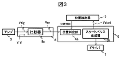
- FIG. 3 is a first configuration example showing details of the light reception state detector 8 and the controller 6.
- the light receiving state detection unit 8 includes a comparator 8a
- the controller 6 includes a position determination unit 6a and a start pulse generator 6b.
- Vref is set to a level higher than the noise level.
- FIG. 4 is a second configuration example showing details of the light reception state detector 8 and the controller 6.
- the light receiving state detection unit 8 includes a level converter 8b and an A / D converter 8c.
- the controller 6 is the same as the first configuration example of FIG.
- the level converter 8b converts the level of the output signal Vsig from the amplifier 3 and outputs it to the A / D converter 8c.
- the A / D converter 8c outputs digital data corresponding to the input signal level to the position determination unit 6a.
- the position determination unit 6a compares the digital data of the A / D converter 8c with a threshold level to determine whether the light reception state or the non-light reception state, and determines whether the position information calculated by the position detector 5 is correct.
- the data communication between the A / D converter 8c and the controller 6 may use either a parallel interface or a serial interface depending on the processing speed and the substrate size. Further, the functions of the A / D converter 8c and the controller 6 may be provided by a single microcomputer.
- the second configuration example uses the level converter 8b, the A / D converter 8c, and the IC having the functions of the controller 6 and has an advantage that no additional components are required for realizing the function of the light receiving state detector 8.
- FIG. 5 is an explanatory diagram of a third configuration example showing details of the light reception state detector 8 and the controller 6.
- FIG. 5A is a first configuration example showing details of the light receiving state detector 8 and the controller 6, and the other configurations are the same as those in FIG.
- FIG. 5B is a diagram showing the relationship between the output signal Vstart of the controller 6, the output signal Vsig of the amplifier 3, and the output signal Ven3 of the light receiving state detector 8.
- the light receiving state detector 8 includes a buffer 8d and a low-pass filter 8e.
- the buffer 8d is provided so as not to affect the preceding light receiving circuit.
- the controller 6 is the same as the first configuration example of FIG.
- the low-pass filter 8e has a function of acquiring an average value of Vsig that is a pulse waveform, and outputs the average value Ven3 to the position determination unit 6a.
- the position determination unit 6a compares the average value Ven3 with a threshold value to determine whether the light reception state or the non-light reception state, and determines whether the position information calculated by the position detector 5 is correct.
- the light reception state detector described in this example is very effective for time measurement using zero cross detection.
- zero cross detection will be described, and problems in the non-light-receiving state and the effectiveness of the light-receiving state detector will be described.
- signal processing in the light receiving state will be described.
- FIG. 6 is an explanatory diagram showing the circuit configuration and principle of zero-cross detection.
- FIG. 6A is a diagram showing a circuit configuration of zero cross detection.
- the circuit configuration includes AC coupling using the capacitance 3 a in the configuration of the amplifier 3, and 0 V is used as the reference voltage of the pulse generator 4.
- a plurality of operational amplifiers are used as a configuration example of the amplifier 3. However, if a sufficient signal level is obtained by the sensor 2, the amplifier may be used alone.
- FIG. 6B shows the principle of zero cross detection.
- the horizontal axis indicates time
- the vertical axis indicates the intensity of the output Vsig of the amplifier 3
- two waveforms when the signal of the amplifier 3 is strong and weak are shown. If the intensity of the output Vsig of the amplifier 3 is different, a deviation occurs in the timing of pulsing when the capacitance 3a is not used.
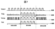
- FIG. 7 is a diagram showing the relationship among the output signal Vstart of the controller 6, the output signal Vsig of the amplifier 3, the output signal Vstop of the pulse generator 4, and the output signal Ven of the light receiving state detector 8.
- the pulse generator 4 compares the noise level of the output signal Vsig of the amplifier 3 with 0V and outputs a random pulse to Vstop. Therefore, there is a problem that the position detector 5 calculates an incorrect position from the Vstop signal in the non-light-receiving state, resulting in erroneous detection.
- the zero cross detection has a problem in that the light receiving state and the non-light receiving state are separated, the Vsig signal in the light receiving state is extracted, and highly accurate position detection is realized.
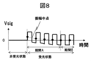
- FIG. 8 is a diagram showing the output Vsig of the amplifier 3 in the light receiving state when zero cross detection is used.
- the dotted line shows the transition of the midpoint of the amplitude of Vsig.
- FIG. 9 is a diagram showing an example of the relationship between the required time from the light receiving state transition to the position detection and the measurement error.
- the light source 1 was driven at a frequency of 1 MHz
- the capacitance 3a was 0.01 uF
- the wiring resistance was 0.5 ⁇ .
- the required time increases, the measurement error decreases, but the measurement cycle increases accordingly.
- the required time must be 39 nsec or more.
- the required time may be determined from the measurement error, or the capacitance 3a may be determined so as to be within an allowable required time.
- FIG. 10 is a diagram showing a method for shortening the time required for position detection.
- FIG. 10A is a diagram showing a configuration in which a signal obtained by passing a low-pass filter as an output Vsig of the amplifier 3 is used as a reference voltage Vref, and is input to the pulse generator 4.
- FIG. FIG. 6 is a diagram illustrating a time transition between a midpoint potential and a reference voltage Vref. As shown in FIG.
- Vref approaches the Vsig intermediate potential from 0 V, and when the period A elapses, the waveform transition is similar to the Vsig midpoint. That is, the configuration shown in FIG. 10A can shorten the time required for position detection as compared with the circuit configuration shown in FIG.
- correct position information may be extracted by signal processing of the position determination unit 6 a in the controller 6.
- FIG. 11 is an explanatory diagram showing a configuration in the position determination unit 6a of the controller 6 and time transition of position information.
- FIG. 11A is a diagram illustrating the configuration of the position determination unit 6a
- FIG. 11B is a diagram illustrating time transition of the position information.
- the position determination unit 6a includes a position information memory 60a and a position information extraction unit 61a.
- the position information memory 60a stores the position information of the position detector 5, and the position information extraction unit 61a extracts correct position information from the signal of the light receiving state detector 8 and the position information transition of the position information memory.
- a method for extracting correct information will be described.
- FIG. 11B immediately after the transition from the non-light-receiving state to the light-receiving state, the target position and the position information are shifted as described above. However, the amount of deviation from the target position decreases with the passage of time, and the position information becomes the target position after the elapse of time t and can be detected. The transition of the position information is monitored, and the position information at the time when the fluctuation of the position information becomes small is extracted. Note that correct position information may be extracted using signal processing in the controller 6.
- a plurality of position information may be used and averaged to calculate correct position information.
- a process of invalidating the first measurement after transition to the light receiving state may be included. For example, when eight pieces of position information are averaged to calculate one measurement data, the measurement data obtained by averaging from the first eight pieces of position information after the light receiving state transition is invalidated, and the next eight pieces of position information are obtained. The measurement data obtained by averaging from is valid. By performing such processing, it is possible to detect a correct position by suppressing a shift in position information due to a time constant.
- FIG. 12 is a diagram showing a configuration for detecting a position using edges of both polarities.
- the position detector 5 includes a positive edge detector 5a, a negative edge detector 5b, and a position calculator 5c.
- the output signal Vstop of the pulse generator 4 is output to the positive edge detector 5a and the negative edge detector 5b.
- the positive edge detector 5a calculates the measurement time from the positive edge of the Vstop signal of the pulse generator 4 and the Vstart signal of the controller 6, and outputs the time measurement value to the position calculator 5c.
- the negative edge detection unit 5b calculates a measurement time from the negative edge of the Vstop signal of the pulse generator 4 and the Vstart signal of the controller 6, and outputs a time measurement value.
- the position calculator 5 c calculates an average value of the measurement results of both edges and outputs position information to the controller 6.
- this embodiment is an optical distance measuring device, which is a light source, a sensor that receives reflected light from an object, and a light receiving state detector that outputs a trigger signal corresponding to the light receiving signal level of the sensor. And a position detector that detects the position of the object from the light reception signal of the sensor, and the light reception state detector is configured to output different signals depending on the light reception state and the non-light reception state of the sensor.
- a method of controlling an optical distance measuring device that detects a position of an object by a time difference or a phase difference between light from a light source and reflected light from the object, and receives the reflected light from the object. And a non-light receiving state in which the reflected light from the object is not received, and the position detection of the object in the light receiving state is made effective based on the detection result.
- the optical distance measuring device As an application example of the optical distance measuring device, a method for realizing low power consumption of the optical distance measuring device, which is used in an image projection apparatus such as a projector and presumes an apparatus for detecting a gesture, will be described. .
- FIG. 13 is a diagram for explaining the appearance of the image projection apparatus 13 according to the present embodiment.
- FIG. 13 shows a side view of the state in which the image projection device 13 is installed on the desk 17.
- the image projection device 13 includes an optical distance measuring device 12, a projection lens 404, a reflection mirror 405, and a focus ring 103.
- the image projection device 13 enlarges the image light generated inside the image projection device with the projection lens 404, reflects the image light with the reflection mirror 405, and projects the image display screen 14 onto the desk 17.
- the desk 17 is a projection plane. The focus of the projected image is adjusted by the focus ring 103.
- the reflection mirror 405 is configured to be foldable, and is stored so that the reflection surface faces the image projection device 13 when not in use.
- the video projection device 13 includes an optical distance measuring device 12 that emits light and detects reflected light of an object.
- the optical distance measuring device 12 may be separate from the image projection device 13.
- the optical distance measuring device 12 detects, for example, the position of the operator's finger and the movement of the finger across the detection boundary 104.
- the image projection device 13 refers to the position and movement of the finger detected by the optical distance measuring device 12, which is called so-called gesture detection, on the screen of a smartphone, tablet, etc. such as tap, flick, swipe, pinch in, and pinch out.
- the video display screen 14 is projected according to the recognized operation.
- FIG. 14 is a block diagram illustrating a functional configuration of the image projection unit 400 of the image projection apparatus 13 according to the present embodiment.
- the image projection unit 400 includes an image control unit 401, a light source 402, a light control unit 403, a projection lens 404, and a reflection mirror 405.
- the video control unit 401 outputs a control signal to the light source 402 and the light control unit 403 according to the video signal supplied from the video signal generator 18.
- the light source 402 is a light source such as a halogen lamp, an LED (Light Emitting Diode), or a laser, and adjusts the amount of light according to a control signal input from the video control unit 401.
- the light control unit 403 includes optical system components such as a mirror, a lens, a prism, and an imager (for example, a display device such as a liquid crystal panel), and uses the light emitted from the light source 402 to output from the video signal generator 18. An optical image based on the supplied image signal is generated.
- the projection lens 404 enlarges the image output from the light control unit 403.
- the reflection mirror 405 reflects the light emitted from the projection lens 404 and projects the image display screen 14 on the desk 17.
- the reflection mirror 405 uses an aspherical mirror, and when projecting an image screen of the same size, the projection distance can be shortened compared to a general image projection apparatus.
- the video signal generator 18 is a general information processing device such as a PC (Personal Computer) connected to the video projection device 13 and a mobile terminal device such as a smartphone.
- the video signal generator 18 sends video signals to the video projection device 13.
- the video signal generator 18 is a device that supplies a video signal to the video projection device 13 such as a card-like storage medium inserted into a card interface provided in the video projection device 13 as well as a PC and a portable terminal device. If it is.
- FIG. 15 is a block diagram showing the configuration of the optical distance measuring device 12 in the present embodiment.
- the optical distance measuring device 12 includes a light source 1, a sensor 2, an amplifier 3, a pulse generator 4, a position detector 5, a controller 6, a driver 7, a light receiving state detector 8, and a scanner 9.
- the controller 6 includes a position detector 6a, a start pulse generator 6b, and a scan signal generator 6c.
- the driver 8 includes a light source driver 7a and a scan driver 7b.
- the light emitted from the light source 1 is scanned (scanned) in a direction corresponding to the angle of the scanner 9 driven by the scan driver 7b, and scanned in a one-dimensional direction or a two-dimensional direction.
- the reflected light of the object 10 is received by the sensor 2 and output to the position determination unit 6 a as position information via the amplifier 3, the pulse generator 4, and the position detector 5.
- the position determination unit 6 a detects correct position information from the position information and the trigger signal of the light receiving state detector 8.
- the signal from the amplifier 3 is output to the position determination unit 6a, the start pulse generator 6b, and the scan signal generator 6c via the light receiving state detector 8.
- the start pulse generator 6b controls the drive timing and supply current of the light source driver 7a from the trigger signal.
- the scan signal generator 6c controls the drive timing and supply current of the scan driver 7b from the trigger signal.
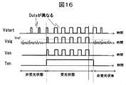
- FIG. 16 shows the output signal Vstart of the start pulse generator 6b, the output signal Vsig of the amplifier 3, the output signal Ven of the light reception state detector 8, and the signal in the position determination unit 6a, which is turned on when Ven continues for a certain period. It is the figure which showed the relationship with the light reception state signal Ten which recognizes a state.
- Vstart which is a driving signal of the light source 1
- Vstart is driven in a low duty state.
- the output Vsig of the amplifier 3 exceeds the reference voltage Vref of the light receiving state detector, so that the light receiving state detector 8 outputs Ven.
- Vref the reference voltage
- the start pulse generator 6b controls a signal for driving the light source driver 7a to control Duty.
- Vstart is driven at a fixed duty in the period when Ten is high, that is, in the light receiving state.
- the power consumption can be reduced by changing the driving method of the light source between the light receiving state and the non-light receiving state.
- the power consumption may be reduced by changing the frequency of the light source 1.
- the frequency of the light source 1 is increased, the number of pulses per unit time increases, and high resolution can be realized when the scanner 9 is driven.
- the power consumption of the driver increases, the light source 1 may be driven at a low frequency in the non-light-receiving state.
- this embodiment is effective for a mobile device driven by a battery.
- the required torque for operating the motor generally increases with a low rotational speed. At low speeds, a larger torque is required, so power is increased. Therefore, it is rotated at high speed in the non-light-receiving state to suppress power consumption, and is rotated at low speed in the light-receiving state. By operating at a low speed in the light receiving state, the scanning speed is slowed down, and high resolution can be realized. For this reason, it is also effective to change the scanner frequency.
- the light source 1 and the scanner 9 are individually operated. However, it goes without saying that a further effect can be obtained by using them in combination.
- FIG. 17 is a diagram for explaining the operation of the scanner 9 when operating the effective area on the video.
- FIG. 17A is a diagram illustrating the operation of the scanner 9 in the non-light receiving state
- FIG. 17B is a diagram illustrating the operation of the scanner 9 in the light receiving state.
- FIG. 17 is a view of the image projection device 13, the optical distance measuring device 12, the image display screen 14, and the screen 15 as viewed from above.
- the scanner 9 is stopped.
- the scanner 9 By stopping the scanner 9, it becomes possible to stop the scan driver 7b, and power consumption can be reduced. Further, since the operation of the scanner 9 is completely stopped, it contributes to a longer life. For example, when a motor is used for the scanner 9, it is possible to prevent the bearings from being worn.
- the hinge part is not stressed, so a long life can be realized.
- the signal generator 6c causes the light reception state detector by blocking light with the finger.
- the scan driver 7b is driven using the 8 Ven signal as a trigger to operate the scanner 9.
- FIG. 18 is a setting flow diagram when the light reception state and the non-light reception state of the scan signal generator 6c are switched in that case.
- the timeout time is TIMEOUT.
- the scan signal generator 6 c determines the state transition based on the Ven signal from the light receiving state detector 8.
- a counter representing the period of the non-light receiving state is incremented.
- the counter value and the TIMEOUT value are compared, and if the counter value is larger than the TIMEOUT value, the state transits to the non-light-receiving state, and the scan driver 7b is driven under conditions according to the non-light-receiving state. If the counter value is smaller than the TIMEOUT value, the current state is maintained.
- the counter In the light receiving state, the counter is only 0, and the time after the transition to the non-light receiving state can be counted. Therefore, by continuing the operation of the scanner 9 for a predetermined time even after the transition to the non-light-receiving state, it is possible to improve the user-friendliness associated with the re-operation of the scanner 9.
- the above is the method for reducing power consumption by controlling the scanner 9.
- FIG. 19 is a diagram showing the positional relationship between the image projection device 13, the optical distance measuring device 12, and the operator 16, and the control block configuration of the optical distance measuring device 12.
- FIG. 19A is a top view of the positional relationship between the image projection device 13 placed on the desk and the operator 16, and FIG. 19B shows the operator 16 in front of the image projection device 13. It is the figure which showed a part of control block structure of the optical distance measuring device 12 assumed the case.
- FIG. 19A is a top view of the positional relationship between the image projection device 13 placed on the desk and the operator 16
- FIG. 19B shows the operator 16 in front of the image projection device 13. It is the figure which showed a part of control block structure of the optical distance measuring device 12 assumed the case.
- FIG. 19A is a top view of the positional relationship between the image projection device 13 placed on the desk and the operator 16
- FIG. 19B shows the operator 16 in front of the image projection device 13. It is the figure which showed a part of control block structure of the optical distance measuring device 12 assumed the case
- reference numeral 17 denotes a desk, which is effective when the operator 16 is outside the effective area, which is the operable area of the display screen 14, although it is in front of the image projection device 13 placed on the desk.
- the sensor 2 receives the reflected light
- the light reception state detection unit 8 determines that the light reception state. For this reason, there is a problem that a sufficient power reduction effect cannot be obtained because the light does not shift to the non-light receiving state even though the reflected light from outside the effective region is received. Therefore, as shown in FIG.
- the optical distance measuring device 12 in the present embodiment is different from that shown in FIG. 15 in that the controller 6 has a light reception state switching unit 6d and an effective area storage unit 6e.
- FIG. 20 is a flow chart for setting the light receiving state and the non-light receiving state of the start pulse generator 6b and the scan signal generator 6c.
- the setting of the light receiving state and the non-light receiving state of the start pulse generator 6b and the scan signal generator 6c may be changed according to the required power reduction effect and application. Only the start pulse generator 6b may be controlled, or both may be controlled. As described with reference to FIG. 18, a timeout may be provided at the time of state transition, and the light receiving state and the non-light receiving state may be switched at an arbitrary timing. According to the present embodiment, if it is not position information of the effective region, it is effective for power reduction by controlling the transition to the non-light-receiving state even in the light-receiving state.
- low power consumption can be realized by devising laser control and scanner control according to the light receiving state and the non-light receiving state.
Landscapes
- Physics & Mathematics (AREA)
- Electromagnetism (AREA)
- Engineering & Computer Science (AREA)
- Computer Networks & Wireless Communication (AREA)
- General Physics & Mathematics (AREA)
- Radar, Positioning & Navigation (AREA)
- Remote Sensing (AREA)
- Optical Radar Systems And Details Thereof (AREA)
Abstract
対象物の位置検出において、非受光状態の誤計測を抑制し高精度な光測距装置を提供することを目的とする。 そのために、光測距装置であって、光源と、対象物からの反射光を受光するセンサと、センサの受光信号レベルに応じたトリガ信号を出力する受光状態検出器と、センサの受光信号から対象物の位置を検出する位置検出器を有し、受光状態検出器はセンサの受光状態と非受光状態で異なる信号を出力するように構成する。
Description
本発明は光を用いた距離測定装置に係り、特に光源とセンサを用いた光測距装置に関する。
物体の位置を検出する方法として一般的に知られているものとして、視差を用い対象物からの反射光の受光位置に応じ距離を算出する三角測量や、投光信号と受光信号の時間差(位相差)により距離を算出するTime-Of-Flight(以下、TOFと記載)がある。いずれの方法においても、対象物からの反射光受光時(以下、受光状態)の信号から位置を計測する必要があるが、対象物からの反射光を受光していない時(以下、非受光状態と記載)のノイズレベルにより対象物の位置を誤検出する場合がある。そのため、従来受光状態と非受光状態を分離し、誤検出のない高精度な計測を行うという課題がある。
この課題に対し、特開2012-26853号公報(特許文献1)では、「時間計測部は、コンパレータから出力される2種類の信号の時間的出現頻度の計測結果に基づいて、その出現頻度が安定した時点における候補ストップ信号をストップ信号に採用する安定化処理を行って光の往復時間を求める」と記載している。
特許文献1では、2種類の信号であるHigh、Low信号のうちHigh信号の時間的出現頻度から正しいストップ信号を決定しているが、時間的出現頻度の設定によっては、非受光状態で誤ったストップ信号を検出し対象物の位置計測に誤りを生じる場合がある。そのため、特許文献1においても誤検出のない高精度な計測を行うべく、受光状態と非受光状態を正確に分離することが課題である。
上記課題を解決するため、本発明は例えば請求の範囲に記載の構成を採用する。本願は上記課題を解決する手段を複数含んでいるが、その一例を挙げるならば、光測距装置であって、光源と、対象物からの反射光を受光するセンサと、センサの受光信号レベルに応じたトリガ信号を出力する受光状態検出器と、センサの受光信号から対象物の位置を検出する位置検出器を有し、受光状態検出器はセンサの受光状態と非受光状態で異なる信号を出力するように構成する。
本発明により測定対象物の位置を高精度に検出可能な光測距装置及びその制御方法を提供できる。
以下、本発明の実施例について図面を用いて説明する。
本実施例では、光測距装置の距離測定原理、構成及び時間計測動作を説明した後、本実施例における受光状態検出器について詳細に説明する。
まず、距離測定原理を説明する。本実施例ではTOFを用いた距離測定を例に説明する。図1は本実施例における距離測定原理の一例を示した図である。図1(a)は光源1、センサ2と対象物10の位置関係を示した図であり、図1(b)は光源1の出射光とセンサ2の受光信号の時間的関係を示した図である。光源1の出射光は対象物10で反射し、センサ2で受光する。光源1の出射光とセンサ2の時間差をt[s]とすると距離L[m]は、光速3.0x10⁸[m]から、下記式(1)
L[m]=光速3.0x10⁸[m]x t[s]/2 (1)
と表される。上記式(1)を用い距離を算出する。
L[m]=光速3.0x10⁸[m]x t[s]/2 (1)
と表される。上記式(1)を用い距離を算出する。
次に、光測距装置の構成を説明する。図2は本実施例における光測距装置12の構成を示したブロック図である。図2において、光測距装置12は、光源1、センサ2、アンプ3、パルス生成器4、位置検出器5、コントローラ6、ドライバ7、受光状態検出器8で構成される。また、11は外部機器、10は対象物である。なお、図2では光源1の光を直線方向に出射する例を示しているが、反射ミラー等を用い1次元方向や2次元方向に走査可能な構成としてもよい。
次に、時間計測動作を説明する。図2において、コントローラ6はドライバ7を駆動するタイミング信号を出力し、ドライバ7はコントローラ6のタイミング信号に応じ光源1を駆動する電流を供給する。光源1はドライバ7の供給電流に応じた強度、タイミングで対象物10に光を出射する。センサ2は対象物10の反射光を受光し、その強度に応じた受光信号をアンプ3に出力する。アンプ3はセンサ2の受光信号を増幅した信号をパルス生成器4、受光状態検出器8に出力する。パルス生成器4はアンプ3の出力信号と参照信号レベルを比較しアナログ信号をパルスに変換し位置検出器5に出力する。位置検出器5はコントローラ6で生成したスタートパルスとパルス生成器4で生成したストップパルスから時間差を算出し対象物の位置を検出した後、位置情報をコントローラ6に出力する。また受光状態検出器8はアンプ3の出力信号レベルに応じ、受光状態もしくは非受光状態を表すトリガ信号をコントローラ6に出力する。コントローラ6は位置検出器5の位置情報と受光状態検出器8の出力信号により対象物の正しい位置を判定する。このように受光状態検出器8により受光状態と非受光状態を分離し、高精度な計測を実現する。また、コントローラ6は、算出した正しい位置情報に応じた制御信号を外部機器11に送信する。外部機器11はPCやスマートフォンやタブレット等の汎用機器、または、USBメモリやSDカード等の外部記録媒体でも良い。また、個別用途として、映像投射装置でも良い。光測距装置12と外部機器11との接続は、例えば、PC等と有線で接続したり、スマートフォンやタブレットなどと無線で接続してもよい。またUSBメモリやSDカード等の外部記録媒体と接続し操作可能としてもよい。以上が光測距装置の時間計測動作である。
次に、図2における受光状態検出器8及びコントローラ6の詳細について説明する。
図3は、受光状態検出器8及びコントローラ6の詳細を示した第1の構成例である。その他の構成は、図2と同様であるので省略する。図3において、受光状態検出部8は比較器8aから構成され、コントローラ6は位置判定部6a、スタートパルス生成器6bから構成される。比較器8aはアンプ3の出力信号Vsigと参照電圧Vrefのレベルを比較し、Vsig≧Vrefの場合Ven=High信号を出力し、Vsig<Vrefの場合Ven=Low信号を位置判定部6aに出力する。このときVrefをノイズレベルより高いレベルに設定する。位置判定部6aは比較器8aの出力信号Venから、位置検出器5で算出した位置情報が正しいか判定を行う。具体的な例を挙げると、Ven=High時は受光状態を示すため、その間位置検出器5から出力される位置情報は正しく、有効なデータであると判定する。このように比較器8aを用い受光状態と非受光状態を分離することで、非受光状態での誤検出をなくし高精度な計測を実現できる。
図3は、受光状態検出器8及びコントローラ6の詳細を示した第1の構成例である。その他の構成は、図2と同様であるので省略する。図3において、受光状態検出部8は比較器8aから構成され、コントローラ6は位置判定部6a、スタートパルス生成器6bから構成される。比較器8aはアンプ3の出力信号Vsigと参照電圧Vrefのレベルを比較し、Vsig≧Vrefの場合Ven=High信号を出力し、Vsig<Vrefの場合Ven=Low信号を位置判定部6aに出力する。このときVrefをノイズレベルより高いレベルに設定する。位置判定部6aは比較器8aの出力信号Venから、位置検出器5で算出した位置情報が正しいか判定を行う。具体的な例を挙げると、Ven=High時は受光状態を示すため、その間位置検出器5から出力される位置情報は正しく、有効なデータであると判定する。このように比較器8aを用い受光状態と非受光状態を分離することで、非受光状態での誤検出をなくし高精度な計測を実現できる。
図4は、受光状態検出器8及びコントローラ6の詳細を示した第2の構成例である。その他の構成は、図2と同様であるので省略する。図4において、受光状態検出部8はレベル変換器8b、A/D変換器8cから構成される。コントローラ6は図3の第1の構成例と同じである。レベル変換器8bはアンプ3の出力信号Vsigをレベル変換しA/D変換器8cに出力する。A/D変換器8cは入力信号レベルに応じたデジタルデータを位置判定部6aに出力する。位置判定部6aはA/D変換器8cのデジタルデータと閾値レベルを比較し受光状態か非受光状態かを判定し、位置検出器5で算出した位置情報が正しいか判定を行う。また、A/D変換器8cとコントローラ6のデータ通信は、処理速度や基板サイズに応じパラレルインターフェース、シリアルインターフェースどちらを用いてもよい。またマイコン1つでA/D変換器8cとコントローラ6の機能を持たせてもよい。第2の構成例はレベル変換器8b、A/D変換器8cとコントローラ6の機能を持つICを用いることで、受光状態検出器8の機能実現に部品の追加が不要となるメリットがある。
図5は、受光状態検出器8及びコントローラ6の詳細を示した第3の構成例の説明図である。図5(a)は受光状態検出器8及びコントローラ6の詳細を示した第1の構成例であり、その他の構成は、図2と同様であるので省略する。図5(b)はコントローラ6の出力信号Vstart、アンプ3の出力信号Vsigと受光状態検出器8の出力信号Ven3の関係を示した図である。
図5(a)において、受光状態検出器8はバッファ8dとローパスフィルタ8eから構成される。バッファ8dは前段の受光回路に影響を及ぼさないよう設けている。コントローラ6は図3の第1の構成例と同じである。図5(b)に示すように、ローパスフィルタ8eはパルス波形であるVsigの平均値を取得する機能を有し、その平均値であるVen3を位置判定部6aに出力する。位置判定部6aは平均値であるVen3と閾値を比較し受光状態か非受光状態かを判定し、位置検出器5で算出した位置情報が正しいか判定を行う。第3の構成例は平均化を行っているため、アンプ3の出力Vsigが安定するまで時間を要するが、比較器やA/D変換器といったICが不要となりコストを低減できるメリットがある。
以上が本実施例の受光状態検出器8の構成、動作詳細である。
以上が本実施例の受光状態検出器8の構成、動作詳細である。
本実施例に記載の受光状態検出器はゼロクロス検出を用いた時間計測に対し非常に有効である。以下ゼロクロス検出を説明し、非受光状態における問題点と受光状態検出器の有効性を説明する。その後受光状態における信号処理を説明する。
まず、ゼロクロス検出を説明する。図6は、ゼロクロス検出の回路構成及び原理を示した説明図である。図6(a)はゼロクロス検出の回路構成を示した図である。回路構成はアンプ3の構成に静電容量3aを用いたAC結合を含み、さらにパルス生成器4の参照電圧に0Vを用いる。図6(a)ではアンプ3の構成例として複数のオペアンプを使用しているが、センサ2で十分な信号レベルが得られれば、アンプを単体で用いてもよい。
次にゼロクロス検出の原理を説明する。図6(b)はゼロクロス検出の原理を示した図である。図6(b)左側の図は静電容量3aを用いず参照電圧Vref>0でパルス化を行う場合を示した図であり、右側の図は静電容量3aを用い参照電圧Vref=0Vでパルス化を行う場合を示した図である。各々、横軸が時間、縦軸がアンプ3の出力Vsigの強度を示し、アンプ3の信号が強い場合と弱い場合の2つの波形を示している。アンプ3の出力Vsigの強度が異なると、静電容量3aを用いない場合はパルス化のタイミングにずれを生じる。つまり対象物の位置が同じでも反射光の強度が異なると計測時間にずれを生じ、位置検出に誤差を生じる。一方静電容量3aを用いた場合、信号強度の強弱によらず信号波形Vsigの振幅中点が0Vとなるため、Vsigの信号強度によらず正確な時間計測を行うことが可能である。つまりゼロクロス検出は受光強度によらず高精度な時間計測が可能な検出方法である。またAC結合の静電容量3aにより定常的に照射される外光による影響を抑制可能である。
次に、ゼロクロス検出の非受光状態における問題点と受光状態検出器の有効性を説明する。図7は、コントローラ6の出力信号Vstart、アンプ3の出力信号Vsig、パルス生成器4の出力信号Vstopと、受光状態検出器8の出力信号Venの関係を示した図である。非受光状態において、パルス生成器4はアンプ3の出力信号Vsigのノイズレベルと0Vを比較しランダムなパルスをVstopに出力する。そのため、位置検出器5が非受光状態のVstop信号から誤った位置を算出し、誤検出となる問題がある。そのため、ゼロクロス検出では、受光状態と非受光状態を分離し、受光状態のVsig信号を抽出し精度の高い位置検出を実現するという課題があった。このような課題に対し、本実施例に記載の受光状態検出器8は受光状態のみVen信号をHighとするため、受光状態と非受光状態を分離できる。これにより、Ven=High期間、つまり受光状態の計測を有効とすることで精度の高い位置検出を行うことができる。
次に、ゼロクロス検出での受光状態における信号処理を説明する。図8はゼロクロス検出を用いた場合の受光状態のアンプ3の出力Vsigを示した図である。点線はVsigの振幅中点の遷移を示している。非受光状態から受光状態に遷移すると、図6(a)に示したように静電容量3aを含む影響でVsigの振幅中点にずれを生じる。遷移後期間Aでは静電容量3aの時定数に応じ時間経過とともに振幅中点と0Vのずれ量が小さくなり、十分時間経過後の期間BではVsigの中点が0Vと一致する。そのため、精度の高い位置検出を行うためには、受光状態遷移後十分時間経過後位置検出を行う。位置検出までの経過時間は静電容量3aの時定数、測定誤差から決定する。
図9は受光状態遷移後から位置検出までの所要時間と測定誤差の関係の一例を示した図である。例では光源1を周波数1MHzで駆動し、静電容量3aを0.01uF、配線抵抗0.5Ωとし算出した。所要時間が増えると測定誤差は小さくなるが、その分測定周期が長くなる。例えば許容誤差1cm以下を目標とする場合、所要時間は39nsec以上設ける必要がある。上述したように所要時間を測定誤差から決定してもよいし、許容可能な所要時間に収まるよう静電容量3aを決定してもよい。
また、パルス生成器4の参照電圧にローパスフィルタを接続し中点に近い電位を入力することで位置検出までの所要時間を短くすることが可能である。これについて以下説明する。図10は位置検出までの所要時間を短縮する方法を示した図である。図10(a)はアンプ3の出力Vsigにローパスフィルタを通した信号を参照電圧Vrefとし、パルス生成器4に入力した構成を示した図であり、図10(b)は受光状態のVsigの中点の電位と参照電圧Vrefの時間遷移を示した図である。図10(b)に示すように、非受光状態から受光状態遷移後、Vrefは0VからVsig中間電位に近づき、期間Aを経過するとVsig中点と同様の波形遷移となる。つまり図10(a)の構成は図6(a)の回路構成と比較し位置検出までの所要時間を短縮可能とできる。
また上記では静電容量3aの時定数を考慮し位置検出する方法を記載したが、コントローラ6内の位置判定部6aの信号処理により正しい位置情報を抽出してもよい。
図11はコントローラ6の位置判定部6a内の構成と位置情報の時間遷移を示した説明図である。図11(a)は位置判定部6aの構成を示した図であり、図11(b)は位置情報の時間遷移を示した図である。
図11(a)に示すように、位置判定部6aは位置情報メモリ60a、位置情報抽出部61aで構成する。位置情報メモリ60aは位置検出器5の位置情報を格納し、位置情報抽出部61aは受光状態検出器8の信号と位置情報メモリの位置情報遷移から正しい位置情報を抽出する。以下、正しい情報の抽出方法を説明する。図11(b)に示すように、非受光状態から受光状態に遷移した直後、前述した通り目標位置と位置情報にずれを生じる。しかし、時間経過とともに目標位置とのずれ量が小さくなり、時間t経過後位置情報が目標位置となるため検出可能となる。この位置情報の遷移を監視し、位置情報の変動が小さくなった時点における位置情報を抽出する。なお、コントローラ6内の信号処理を用い正しい位置情報を抽出してもよい。
また、精度のよい測定を行う場合、位置情報を複数用い、平均化を行い正しい位置情報を算出してもよい。その場合、受光状態に遷移した最初の測定は無効とする処理を入れてもよい。例えば8個の位置情報を平均化し一つの測定データを算出する場合、受光状態遷移後の最初の8個の位置情報から平均化により得られた測定データを無効とし、次の8個の位置情報から平均化により得られた測定データを有効とする。このような処理を行うことで時定数による位置情報のずれを抑制し正しい位置検出が可能となる。
次に、上記と異なり受光状態遷移直後に位置情報を検出可能な方法について説明する。すなわち、パルス生成器4の出力のポジティブエッジ(立上りエッジ)、ネガティブエッジ(立下りエッジ)両方を用い時間計測を行う。以下詳細に説明する。図12は両極性のエッジを用い位置を検出する構成を示した図である。図12に示すように、位置検出器5は、ポジティブエッジ検出部5a、ネガティブエッジ検出部5b、位置計算器5cで構成する。パルス生成器4の出力信号Vstopは、ポジティブエッジ検出部5a、ネガティブエッジ検出部5bに出力される。ポジティブエッジ検出部5aは、パルス生成器4のVstop信号のポジティブエッジとコントローラ6のVstart信号から計測時間を算出し位置計算器5cに時間計測値を出力する。ネガティブエッジ検出部5bは、パルス生成器4のVstop信号のネガティブエッジとコントローラ6のVstart信号から計測時間を算出し時間計測値を出力する。位置計算器5cは、両エッジの計測結果の平均値を計算し位置情報をコントローラ6に出力する。以上の処理を行うことで受光状態遷移から一定時間経過後に取得する処理は不要となる。ただし検出部が多くなりコストが高くなるため、コスト低減を優先する場合は前述した片側エッジを用いた方法を用いた方が好ましい。以上がゼロクロス検出での受光状態における信号処理である。
以上のように、本実施例は、光測距装置であって、光源と、対象物からの反射光を受光するセンサと、センサの受光信号レベルに応じたトリガ信号を出力する受光状態検出器と、センサの受光信号から対象物の位置を検出する位置検出器を有し、受光状態検出器はセンサの受光状態と非受光状態で異なる信号を出力するように構成する。
また、光源の光と該光の対象物からの反射光との時間差または位相差により対象物の位置を検出する光測距装置の制御方法であって、対象物からの反射光を受光している受光状態と、対象物からの反射光を受光していない非受光状態を検出し、該検出結果に基づき受光状態での対象物の位置検出を有効とするように構成する。
これにより、測定対象物の位置を高精度に検出可能な光測距装置及びその制御方法を提供できる。
本実施例は、光測距装置の適用例として、プロジェクタのような映像投写装置に用い、ジェスチャ検出を行う装置を前提とした、光測距装置の低消費電力化を実現する方法について説明する。
図13は、本実施例に係る映像投写装置13の外観を説明する図である。図13は、映像投写装置13を机17上に設置した状態を横から見た図を示している。図13に示すように、映像投写装置13は、光測距装置12、投写レンズ404、反射ミラー405、フォーカスリング103から構成される。映像投写装置13は、映像投写装置内部で生成した映像光を投写レンズ404で拡大した後、反射ミラー405で反射して机17に映像表示画面14を投写する。図13においては、机17が投写面である。投射映像のフォーカスは、フォーカスリング103で調整される。反射ミラー405は、折り畳み可能に構成されており、不使用時には反射面が映像投写装置13と対向するように収納される。また、映像投写装置13は、光を出射し物体の反射光を検知する光測距装置12を有している。なお、光測距装置12は映像投写装置13と別体でもよい。光測距装置12は、例えば、検出境界104を横切った操作者の指の位置及び指の動きを検知する。これにより、映像投写装置13は、いわゆる、ジェスチャ検出と呼ばれる、光測距装置12が検知した指の位置及び動きを、タップ、フリック、スワイプ、ピンチイン、ピンチアウト等のスマートフォン、タブレット等の画面上で行われる操作と同様の操作として認識し、認識した操作に応じた映像表示画面14を投写する。
図14は本実施例に係る映像投写装置13の映像投写部400の機能構成を示すブロック図である。図14に示すように、映像投写部400は、映像制御部401、光源402、光制御部403、投写レンズ404及び反射ミラー405を含む。まず映像投写部400の機能を説明する。映像制御部401は、映像信号発生器18から供給された映像信号に応じて、光源402、光制御部403に対して制御信号を出力する。光源402は、ハロゲンランプ、LED(Light Emitting Diode)、レーザ等の光源であり、映像制御部401から入力された制御信号に応じて光量を調整する。なお、光源402は、R(Red)、G(Green)、B(Blue)の3色を含む場合、映像信号に応じて各々独立して光量を制御してもよい。光制御部403は、ミラー、レンズ、プリズム、イメージャ(例えば液晶パネルのような表示デバイス)等の光学系構成要素を有し、光源402から出射された光を用いて、映像信号発生器18から供給された映像信号に基づく光学的な映像を生成する。投写レンズ404は、光制御部403から出力された映像を拡大する。反射ミラー405は、投写レンズ404から放射された光を反射し、机17に映像表示画面14を投写する。反射ミラー405は、非球面ミラーを用いており、同サイズの映像画面を投写する場合、一般的な映像投写装置と比較して投写距離を短くすることができる。
本実施例においては、反射ミラー405を用いた映像投写部400を例として説明したが、映像投写を実現できる構成であれば他の構成でもよい。また、映像信号発生器18は、映像投写装置13と接続されたPC(Personal Computer)等の一般的な情報処理装置及びスマートフォン等の携帯端末装置であり、映像投写装置13に対して映像信号を供給する。なお、映像信号発生器18は、PC及び携帯端末装置に限らず、映像投写装置13に備えられたカードインタフェースに挿入されるカード状の記憶媒体等、映像投写装置13に映像信号を供給する装置であればよい。
図15は本実施例における光測距装置12の構成を示したブロック図である。図15において、光測距装置12は、光源1、センサ2、アンプ3、パルス生成器4、位置検出器5、コントローラ6、ドライバ7、受光状態検出器8、スキャナ9から構成される。コントローラ6は位置検出部6a、スタートパルス生成器6b、スキャン信号生成器6cで構成する。ドライバ8は、光源ドライバ7a、スキャンドライバ7bで構成する。
次に動作を説明する。なお本実施例における構成の実施例1の図2と重複する機能に関しては説明を省略する。光源1の出射光は、スキャンドライバ7bにより駆動されたスキャナ9の角度に応じた向きにスキャン(走査)され、1次元方向もしくは2次元方向にスキャンされる。対象物10の反射光はセンサ2で受光され、アンプ3、パルス生成器4、位置検出器5を介し位置情報として位置判定部6aに出力される。位置判定部6aは位置情報と受光状態検出器8のトリガ信号から正しい位置情報を検出する。またアンプ3の信号は受光状態検出器8を介し、トリガ信号を位置判定部6a、スタートパルス生成器6b、スキャン信号生成器6cに出力される。スタートパルス生成器6bはトリガ信号から光源ドライバ7aの駆動タイミング、供給電流を制御する。スキャン信号生成器6cはトリガ信号からスキャンドライバ7bの駆動タイミング、供給電流を制御する。以上が本実施例の光測距装置の構成、動作である。
次に、スタートパルス生成器6b及びスキャン信号生成器6cの動作詳細を説明する。図16はスタートパルス生成器6bの出力信号Vstart、アンプ3の出力信号Vsig、受光状態検出器8の出力信号Ven、及び位置判定部6a内の信号であってVenが一定周期続くとONする受光状態を認識する受光状態信号Ten、との関係を示した図である。
ここでは、非受光状態においては光源1を駆動するDutyを低くし低消費電力を実現する例を示している。この動作について以下説明する。
図16において、非受光状態においては、光源1の駆動信号であるVstartをDutyの低い状態で駆動する。対象物からの反射光を検出するとアンプ3の出力Vsigが受光状態検出器の参照電圧Vrefを超えるため受光状態検出器8からVenが出力される。Venが出力されると受光状態に遷移し受光状態信号TenがHighとなる。スタートパルス生成器6bはVenがHighになると光源ドライバ7aを駆動する信号を制御しDutyを制御する。VstartはTenがHighの期間、すなわち受光状態では一定のDutyで駆動する。そして、非受光状態となりVenがLowとなると非受光状態に遷移しTenがLowとなり、VstartをDutyの低い状態に切替える。このように受光状態と非受光状態で光源の駆動方法を変更することで低消費電力化を可能とする。
なお、上記でDutyを制御する例を示したが、Vrefを超えるレベルの強度を確保すれば振幅を制御してもよい。また光源1の周波数を変更することで低消費電力化を図ってもよい。光源1の周波数を高くすると単位時間当たりのパルス回数が多くなり、スキャナ9を駆動している際は高解像度化を実現できる。しかしドライバの電力消費が大きくなるため、非受光状態では光源1を低い周波で駆動してもよい。特に本実施例は電池で駆動するモバイル機器に有効である。
またスキャナ9の周波数を変更し走査速度を切り替えることも有効である。例えばスキャナ9にポリゴンモータを用いた場合について説明する。モータを動作させる必要トルクは一般的に回転数が低いと高くなる。低速ではより大きなトルクが必要となるため電力が大きくなる。そのため非受光状態では高速で回転させ電力消費を抑え、受光状態では低速で回転させる。受光状態では低速で動作させることで走査速度が遅くなり高解像度化を実現できる。このような理由でスキャナの周波数を変更することも有効である。なお、本実施例では光源1とスキャナ9を個々に動作させる記述をしたが、組合せで使用することでさらに効果が得られることは言うまでもない。
次に、映像投写装置を用い、表示画面上の限られた領域を有効領域とする場合に有効な低消費電力化の方法を説明する。図17は映像上の有効領域を操作する場合のスキャナ9の動作を説明する図である。図17(a)は非受光状態のスキャナ9の動作を説明する図であり、図17(b)は受光状態のスキャナ9の動作を示した図である。
図17は映像投写装置13、光測距装置12、映像表示画面14、スクリーン15を上面から見た図である。図17(a)のように、対象物10が映像表示画面14内にない場合、つまり非受光状態ではスキャナ9を停止する。スキャナ9を停止することでスキャンドライバ7bを停止することが可能となり低消費電力化を図れる。またスキャナ9の動作を完全に停止するため、長寿命化にも寄与する。例えばスキャナ9にモータを用いる場合、軸受けの磨耗を防ぐことが可能となる。またMEMSミラーを用いた場合はヒンジ部に応力がかからないため長寿命化を実現できる。
図17(b)のように、例えば対象物10として操作者の指である場合、指が映像表示画面14内にある場合、指により光を遮ることによって、信号生成器6cは受光状態検出器8のVen信号をトリガとしスキャンドライバ7bを駆動しスキャナ9を動作させる。動作後は、指が光源のスキャン範囲外に移動した場合に対応して、スキャナ9は受光状態検出部8のVen=Lowによって受光状態から非受光状態へ遷移してもよいし、一定時間スキャンしタイムアウトしてもよい。また、例えば画面上の指を検出し、画面をタッチした後に指が光源のスキャン範囲外に移動した場合、非受光状態に遷移しスキャナ9を停止させるようにしてもよい。
なお、一旦停止するとスキャナ9を再度動作させるため、映像投写装置13正面にある光を遮ることがスキャンのトリガとなっている場合、映像投写装置13正面にある光を反射する必要がありユーザとして使いにくい場合がある。そのため用途に応じて非受光状態に遷移してもタイムアウト時間を設けスキャナ9の動作制御を行ってもよい。図18は、その場合の、スキャン信号生成器6cの受光状態、非受光状態切替時の設定フロー図である。ここでタイムアウト時間をTIMEOUTとする。スキャン信号生成器6cは受光状態検出器8のVen信号により状態遷移の判定を行う。Ven=Lowの場合、まず非受光状態の期間を表すcounterをインクリメントする。次にcounter値とTIMEOUT値を比較し、counter値がTIMEOUT値より大きければ非受光状態に遷移し、非受光状態に応じた条件でスキャンドライバ7bを駆動する。counter値がTIMEOUT値より小さければ現在の状態を維持する。Ven=Highの場合、受光状態に遷移し受光状態に応じた条件でスキャンドライバ7bを駆動する。このとき非受光状態の期間を表すcounterに0を入力する。受光状態ではcounterは0の状態のみとし、非受光状態に遷移してからの時間をカウント可能な構成とする。よって非受光状態に遷移してからも所定時間スキャナ9の動作を続けることで、スキャナ9の再動作に伴うユーザの使い勝手を向上することができる。以上がスキャナ9の制御による低消費電力化の方法である。
次に、有効領域の位置情報でなければ受光状態でも非受光状態に遷移する制御とすることも電力低減に有効である。以下、その場合の受光状態から非受光状態に遷移する方法を説明する。図19は映像投写装置13と光測距装置12、操作者16の位置関係と、光測距装置12の制御ブロック構成を示した図である。図19(a)は机上に置かれた映像投写装置13と操作者16の位置関係を上から見た図であり、図19(b)は映像投写装置13の正面に操作者16が存在する場合を想定した光測距装置12の制御ブロック構成の一部を示した図である。図19(a)において、17は机であって、机上に置かれた映像投写装置13の正面ではあるが表示画面14の操作可能な領域である有効領域外に操作者16がいる場合、有効領域に例えば指で操作するような行動をとっていない場合でも、光測距装置12から出射した光は操作者16で反射し、その反射光をセンサ2で受光する。センサ2が反射光を受光すると受光状態検出部8が受光状態と判定する。そのため有効領域外からの反射光を受光したにも関わらず非受光状態に移行せず、十分な電力低減効果が得られないという問題がある。そこで、図19(b)に示すように、本実施例における光測距装置12は、図15と異なり、コントローラ6は受光状態切替部6d、有効領域格納部6eを有する。受光状態切替部6dは位置判定部6aの位置情報と有効領域格納部6eのデータを比較し、位置情報が有効領域内のデータであるか判断する。その後スタートパルス生成器6b、スキャン信号生成器6cに切替信号Vstateを出力する。もし有効領域の位置情報でなければ、Vstate = Lowを出力し、受光状態切替部を受けたスタートパルス生成器6b、スキャン信号生成器6cは非受光状態に遷移する。
図20はスタートパルス生成器6bとスキャン信号生成器6cの受光状態、非受光状態の設定フロー図である。図20において、まずスタートパルス生成器6bとスキャン信号生成器6cは、受光状態切替部6dのVstate信号により条件分岐を行う。Vstate=Lowであれば非受光状態に遷移し非受光状態に応じた条件でドライバ7を駆動する。Vstate=Highであれば受光状態検出器8のVen信号により条件分岐を行う。Ven=Lowであれば非受光状態に応じた条件でドライバ7を駆動する。Ven=Highであれば受光状態に応じた条件でドライバ7を駆動する。前述したがスタートパルス生成器6bとスキャン信号生成器6cの受光状態、非受光状態の設定は必要な電力低減効果、用途に応じて変更してよい。スタートパルス生成器6bのみ制御を行ってもよいし、両方制御してもよい。また図18で説明したように、状態遷移時にタイムアウトを設け、任意のタイミングで受光状態、非受光状態を切替えても良い。本実施例によれば、有効領域の位置情報でなければ受光状態でも非受光状態に遷移する制御とすることで電力低減に有効となる。
以上のように、本実施例によれば受光状態、非受光状態に応じてレーザ制御、スキャナ制御を工夫することで低消費電力化を実現できる。
なお、上記した実施例は本発明を分かりやすく説明するために詳細に説明したものであり、必ずしも説明した全ての構成を備えるものに限定されるものではない。また、ある実施例の構成の一部を他の実施例の構成に置き換えることが可能であり、また、ある実施例の構成に他の実施例の構成を加えることも可能である。また、各実施例の構成の一部について、他の構成の追加・削除・置換をすることが可能である。
1:光源、2:センサ、3:アンプ、3a:静電容量、4:パルス生成器、5:位置検出器、5a:ポジティブエッジ検出部、5b:ネガティブエッジ検出部 、5c:位置計算器 、6:コントローラ 、6a:位置判定部 、6b:スタートパルス生成器、6c:スキャン信号生成器、6d:受光状態切替部、6e:有効領域格納部、60a:位置情報メモリ 、61a:位置情報抽出部 、7:ドライバ 、7a:光源ドライバ、7b:スキャンドライバ、8:受光状態検出器 、8a:比較器 、8b:レベル変換器 、8c:A/D変換器 、8d:バッファ 、8e:ローパスフィルタ 、10:対象物、11:外部機器、12:光測距装置、13:映像投写装置、14:映像表示画面、15:スクリーン、16:操作者、17:机、18:映像信号発生器
Claims (15)
- 光源と、
対象物からの反射光を受光するセンサと、
前記センサの受光信号レベルに応じたトリガ信号を出力する受光状態検出器と、
前記センサの受光信号から前記対象物の位置を検出する位置検出器を有し、
前記受光状態検出器は前記センサの受光状態と非受光状態で異なる信号を出力することを特徴とする光測距装置。 - 請求項1に記載の光測距装置であって、
前記受光状態検出器は信号レベルと参照電圧を比較しパルスを出力する比較器であることを特徴とする光測距装置。 - 請求項1に記載の光測距装置であって、
前記受光状態検出器はA/D変換器であることを特徴とする光測距装置。 - 請求項1に記載の光測距装置であって、
前記受光状態検出器はバッファとローパスフィルタで構成することを特徴とする光測距装置。 - 請求項1に記載の光測距装置であって、
前記光源からの光を1次元方向、もしくは2次元方向に走査することを特徴とする光測距装置。 - 請求項5に記載の光測距装置であって、
前記光源からの光は、前記受光状態検出器のトリガ信号に応じて受光状態、非受光状態で発光Duty及び/または振幅及び/または周波数を切替えることを特徴とする光測距装置。 - 請求項5に記載の光測距装置であって、
前記光源からの光は、前記受光状態検出器のトリガ信号に応じて受光状態、非受光状態で走査速度を切替えることを特徴とする光測距装置。 - 請求項5に記載の光測距装置であって、
前記光源からの光は、前記受光状態検出器のトリガ信号に応じて非受光状態で走査を停止することを特徴とする光測距装置。 - 請求項5に記載の光測距装置であって、
前記光源からの光を、前記受光状態検出器のトリガ信号入力後から所定期間後に該トリガ信号に応じた受光状態と非受光状態での動作に切替えることを特徴とする光測距装置。 - 請求項1に記載の光測距装置であって、
さらに前記センサの受光信号をパルス化するパルス生成器を備え、
前記位置検出器は前記光源の出射光と前記パルス生成器から出力するパルスの時間差から対象物までの距離を計測することを特徴とする光測距装置。 - 請求項10に記載の光測距装置であって、
前記パルス生成器は前記センサの受光信号をACカップリングした信号とGNDレベルの基準電圧を比較しパルス生成することを特徴とする光測距装置。 - 請求項10に記載の光測距装置であって、
前記受光状態検出器のトリガ信号入力後から所定期間後に前記位置検出器から出力する位置情報を有効とすることを特徴とする光測距装置。 - 請求項11に記載の光測距装置であって、
前記位置検出器は前記パルス生成器の出力パルスの立上り、立下り両エッジを検出し時間計測することを特徴とする光測距装置。 - 光源の光と該光の対象物からの反射光との時間差または位相差により該対象物の位置を検出する光測距装置の制御方法であって、
前記対象物からの反射光を受光している受光状態と、前記対象物からの反射光を受光していない非受光状態を検出し、
該検出結果に基づき前記受光状態での前記対象物の位置検出を有効とすることを特徴とする光測距装置の制御方法。 - 映像投写装置と光測距装置を有するジェスチャ検出装置であって、
前記光測距装置は、光源と、対象物からの反射光を受光するセンサと、前記センサの受光状態と非受光状態で異なる信号を出力する受光状態検出器と、前記受光状態検出器からの信号と前記センサの受光信号から前記受光状態での前記対象物の位置検出信号を出力する位置検出器を有し、
前記位置検出信号により、対象物の操作を認識し、該認識した操作に応じた映像表示を前記映像投写装置により投写することを特徴とするジェスチャ検出装置。
Priority Applications (1)
| Application Number | Priority Date | Filing Date | Title |
|---|---|---|---|
| PCT/JP2015/066852 WO2016199267A1 (ja) | 2015-06-11 | 2015-06-11 | 光測距装置及びその制御方法、及びそれを用いたジェスチャ検出装置 |
Applications Claiming Priority (1)
| Application Number | Priority Date | Filing Date | Title |
|---|---|---|---|
| PCT/JP2015/066852 WO2016199267A1 (ja) | 2015-06-11 | 2015-06-11 | 光測距装置及びその制御方法、及びそれを用いたジェスチャ検出装置 |
Publications (1)
| Publication Number | Publication Date |
|---|---|
| WO2016199267A1 true WO2016199267A1 (ja) | 2016-12-15 |
Family
ID=57504864
Family Applications (1)
| Application Number | Title | Priority Date | Filing Date |
|---|---|---|---|
| PCT/JP2015/066852 Ceased WO2016199267A1 (ja) | 2015-06-11 | 2015-06-11 | 光測距装置及びその制御方法、及びそれを用いたジェスチャ検出装置 |
Country Status (1)
| Country | Link |
|---|---|
| WO (1) | WO2016199267A1 (ja) |
Citations (12)
| Publication number | Priority date | Publication date | Assignee | Title |
|---|---|---|---|---|
| JPS57180234A (en) * | 1981-04-30 | 1982-11-06 | Tokyo Juki Ind Co Ltd | Malfunction preventing circuit for photodetector |
| JPH10253767A (ja) * | 1997-03-07 | 1998-09-25 | Atsumi Electron Corp Ltd | 熱線センサ |
| JP2001298353A (ja) * | 2000-04-17 | 2001-10-26 | Atsumi Electric Co Ltd | 開閉検知センサ |
| JP2002347580A (ja) * | 2001-05-25 | 2002-12-04 | Denso Corp | 車両用侵入検出装置 |
| JP2007334515A (ja) * | 2006-06-13 | 2007-12-27 | Sharp Corp | 防犯装置 |
| JP2012026853A (ja) * | 2010-07-22 | 2012-02-09 | Panasonic Electric Works Co Ltd | 距離センサ |
| JP2012211845A (ja) * | 2011-03-31 | 2012-11-01 | Secom Co Ltd | 赤外線センサ |
| JP2014164205A (ja) * | 2013-02-27 | 2014-09-08 | Hitachi Consumer Electronics Co Ltd | ビーム走査型表示装置 |
| JP2014202610A (ja) * | 2013-04-05 | 2014-10-27 | 日立コンシューマエレクトロニクス株式会社 | 光測距装置 |
| WO2015045125A1 (ja) * | 2013-09-27 | 2015-04-02 | 日立マクセル株式会社 | 映像投射装置 |
| WO2015092905A1 (ja) * | 2013-12-19 | 2015-06-25 | 日立マクセル株式会社 | 投写型映像表示装置及び投写型映像表示方法 |
| JP2015125670A (ja) * | 2013-12-27 | 2015-07-06 | 日立マクセル株式会社 | 画像投射装置 |
-
2015
- 2015-06-11 WO PCT/JP2015/066852 patent/WO2016199267A1/ja not_active Ceased
Patent Citations (12)
| Publication number | Priority date | Publication date | Assignee | Title |
|---|---|---|---|---|
| JPS57180234A (en) * | 1981-04-30 | 1982-11-06 | Tokyo Juki Ind Co Ltd | Malfunction preventing circuit for photodetector |
| JPH10253767A (ja) * | 1997-03-07 | 1998-09-25 | Atsumi Electron Corp Ltd | 熱線センサ |
| JP2001298353A (ja) * | 2000-04-17 | 2001-10-26 | Atsumi Electric Co Ltd | 開閉検知センサ |
| JP2002347580A (ja) * | 2001-05-25 | 2002-12-04 | Denso Corp | 車両用侵入検出装置 |
| JP2007334515A (ja) * | 2006-06-13 | 2007-12-27 | Sharp Corp | 防犯装置 |
| JP2012026853A (ja) * | 2010-07-22 | 2012-02-09 | Panasonic Electric Works Co Ltd | 距離センサ |
| JP2012211845A (ja) * | 2011-03-31 | 2012-11-01 | Secom Co Ltd | 赤外線センサ |
| JP2014164205A (ja) * | 2013-02-27 | 2014-09-08 | Hitachi Consumer Electronics Co Ltd | ビーム走査型表示装置 |
| JP2014202610A (ja) * | 2013-04-05 | 2014-10-27 | 日立コンシューマエレクトロニクス株式会社 | 光測距装置 |
| WO2015045125A1 (ja) * | 2013-09-27 | 2015-04-02 | 日立マクセル株式会社 | 映像投射装置 |
| WO2015092905A1 (ja) * | 2013-12-19 | 2015-06-25 | 日立マクセル株式会社 | 投写型映像表示装置及び投写型映像表示方法 |
| JP2015125670A (ja) * | 2013-12-27 | 2015-07-06 | 日立マクセル株式会社 | 画像投射装置 |
Similar Documents
| Publication | Publication Date | Title |
|---|---|---|
| EP2120455B1 (en) | Electronics device having projector module | |
| CN109643045B (zh) | 投影仪的非接触式控制 | |
| US8873069B2 (en) | Motion sensing method for determining whether to perform motion sensing according to distance detection result and related apparatus thereof | |
| EP2239650A2 (en) | Image display apparatus, image display method, and recording medium having image display program stored therein | |
| US8830210B2 (en) | Optical touch apparatus and drive method to control an average brightness of LEDs | |
| US8582118B2 (en) | Optical detecting device, display device, and electronic equipment | |
| US10216331B2 (en) | Touch projection system and touch sensitivity adjusting method thereof | |
| EP3051345B1 (en) | Video projection device | |
| US8791925B2 (en) | Coordinate input apparatus, control method therefor and program | |
| US20190028659A1 (en) | Image processing device | |
| US10345937B2 (en) | Electronic device with a backlight and capacitive touch panel and method for controlling electronic device so as to suppress error detection of a touch operation | |
| KR102219981B1 (ko) | 레이저 프로젝션 디스플레이 및 그의 컬러 얼라인먼트 방법 | |
| US20150116276A1 (en) | Projector | |
| US20100060567A1 (en) | Controlling device operation relative to a surface | |
| US20200240815A1 (en) | Distance measuring device and method thereof for seeking distance measuring starting point | |
| JP2017017420A (ja) | 光電センサ | |
| WO2017212601A1 (ja) | 光測距装置、及びこれを備えた映像投写装置 | |
| JP2011099994A (ja) | 位置検出機能付き投射型表示装置 | |
| JP6359763B2 (ja) | 光検出装置および電子機器 | |
| US10331273B2 (en) | Touch display system, touch device and touch display method for avoiding misjudging of touch position | |
| CN103809351B (zh) | 具检测投影画面变形的光学投影系统及其检测方法 | |
| JP2013003997A (ja) | 光学式位置検出装置および入力機能付き表示システム | |
| JP6246011B2 (ja) | 位置検出装置及びタッチパネル装置 | |
| WO2017064787A1 (ja) | 光測距装置、光測距方法、及び、それを備えた映像投写装置 | |
| WO2017038025A1 (en) | Imaging apparatus |
Legal Events
| Date | Code | Title | Description |
|---|---|---|---|
| 121 | Ep: the epo has been informed by wipo that ep was designated in this application |
Ref document number: 15894952 Country of ref document: EP Kind code of ref document: A1 |
|
| NENP | Non-entry into the national phase |
Ref country code: DE |
|
| NENP | Non-entry into the national phase |
Ref country code: JP |
|
| 122 | Ep: pct application non-entry in european phase |
Ref document number: 15894952 Country of ref document: EP Kind code of ref document: A1 |