WO2016194876A1 - 発光装置およびその製造方法 - Google Patents
発光装置およびその製造方法 Download PDFInfo
- Publication number
- WO2016194876A1 WO2016194876A1 PCT/JP2016/065931 JP2016065931W WO2016194876A1 WO 2016194876 A1 WO2016194876 A1 WO 2016194876A1 JP 2016065931 W JP2016065931 W JP 2016065931W WO 2016194876 A1 WO2016194876 A1 WO 2016194876A1
- Authority
- WO
- WIPO (PCT)
- Prior art keywords
- light emitting
- light
- emitting device
- phosphor
- emitting elements
- Prior art date
- Legal status (The legal status is an assumption and is not a legal conclusion. Google has not performed a legal analysis and makes no representation as to the accuracy of the status listed.)
- Ceased
Links
Images








Classifications
-
- H—ELECTRICITY
- H10—SEMICONDUCTOR DEVICES; ELECTRIC SOLID-STATE DEVICES NOT OTHERWISE PROVIDED FOR
- H10H—INORGANIC LIGHT-EMITTING SEMICONDUCTOR DEVICES HAVING POTENTIAL BARRIERS
- H10H20/00—Individual inorganic light-emitting semiconductor devices having potential barriers, e.g. light-emitting diodes [LED]
- H10H20/80—Constructional details
- H10H20/85—Packages
-
- H—ELECTRICITY
- H10—SEMICONDUCTOR DEVICES; ELECTRIC SOLID-STATE DEVICES NOT OTHERWISE PROVIDED FOR
- H10H—INORGANIC LIGHT-EMITTING SEMICONDUCTOR DEVICES HAVING POTENTIAL BARRIERS
- H10H20/00—Individual inorganic light-emitting semiconductor devices having potential barriers, e.g. light-emitting diodes [LED]
- H10H20/80—Constructional details
- H10H20/85—Packages
- H10H20/851—Wavelength conversion means
-
- H—ELECTRICITY
- H10—SEMICONDUCTOR DEVICES; ELECTRIC SOLID-STATE DEVICES NOT OTHERWISE PROVIDED FOR
- H10W—GENERIC PACKAGES, INTERCONNECTIONS, CONNECTORS OR OTHER CONSTRUCTIONAL DETAILS OF DEVICES COVERED BY CLASS H10
- H10W90/00—Package configurations
- H10W90/701—Package configurations characterised by the relative positions of pads or connectors relative to package parts
- H10W90/751—Package configurations characterised by the relative positions of pads or connectors relative to package parts of bond wires
- H10W90/753—Package configurations characterised by the relative positions of pads or connectors relative to package parts of bond wires between laterally-adjacent chips
Definitions
- the present invention relates to a light emitting device and a method for manufacturing the same.
- a COB (Chip On Board) light emitting device in which a light emitting element such as an LED (light emitting diode) element is mounted on a general-purpose substrate such as a ceramic substrate or a metal substrate is known.
- a light emitting element such as an LED (light emitting diode) element
- a general-purpose substrate such as a ceramic substrate or a metal substrate
- an LED element that emits blue light is sealed with a resin containing a phosphor, and light obtained by exciting the phosphor with light from the LED element is mixed, depending on the application. White light is obtained.
- Patent Document 1 discloses a highly heat-conductive heat radiation base having a mounting surface for die bonding, a hole that is placed on the heat radiation base and exposes a part of the mounting surface, and an outside of the heat radiation base.
- a circuit board having a projecting portion projecting outward from the periphery, a light emitting element mounted on the mounting surface through the hole, and a translucent resin body that seals the upper side of the light emitting element;
- a light emitting diode in which a through hole that is electrically connected to a light emitting element is formed on the outer peripheral edge of the protruding portion, and an external connection electrode is provided on the upper and lower surfaces of the through hole.
- Patent Document 2 discloses a cavity in which a recess is formed, a convex heat slug (pedestal) attached to the cavity so as to penetrate the bottom of the recess, and a submount substrate mounted on the heat slug. And a plurality of LED chips arranged on the submount substrate, a lead frame electrically connected to each LED chip, a phosphor layer enclosing each LED chip, and a silicone resin sealed in the recess. An LED package having a lens is described.
- Patent Document 3 includes a step of forming a liquid repellent pattern on a substrate, a step of mounting an LED chip inside the liquid repellent pattern on the substrate, and a sealing resin in which a phosphor is kneaded inside the liquid repellent pattern.
- a method for manufacturing a light emitting device package is described which includes a step of applying and a step of precipitating the phosphor in the sealing resin in a windless state.
- the actual color of the emitted light may be different from the color of the target light.
- the light emitting elements are mounted with a certain distance between them to prevent a short circuit. Therefore, any part of the light emitting element is included in the portion of the sealing resin that fills the space between the light emitting elements. This is because the light passing distance in the phosphor layer is different depending on whether light is emitted from the phosphor layer.
- the light transmission distance in the phosphor layer changes depending on the emission position and emission direction from the light emitting element, and the intensity of the light of the color corresponding to the phosphor also changes accordingly. It becomes difficult to match.
- the present invention provides the actual light color obtained by mixing the light emitted from a plurality of light-emitting elements mounted at high density and the excitation light from the phosphor contained in the resin that seals the light-emitting elements. It is an object of the present invention to provide a light emitting device and a method for manufacturing the same, in which deviation from a design value is suppressed as much as possible.
- a light-emitting device which is mounted on a substrate so that the distance between elements is 5 ⁇ m or more and 120% or less of the average particle diameter of the phosphor.
- a plurality of light emitting elements densely mounted on the substrate with the light emitting surface facing away from the substrate, and a plurality of types of phosphors excited by light from the plurality of light emitting elements And a sealing resin that seals the whole of the plurality of light emitting elements, the interval between adjacent light emitting elements is 5 ⁇ m or more, and a plurality of types of fluorescent light
- a light emitting device characterized in that the length is 120% or less of the median diameter D50 of the phosphor having the largest average particle diameter among the bodies.
- the median diameter D50 is preferably 20 ⁇ m or more and 25 ⁇ m or less.
- the light emitting device preferably further includes an optical element placed on the substrate so as to cover the sealing resin.
- the method includes a step of mounting a plurality of light emitting elements densely on a substrate and a step of sealing the whole of the plurality of light emitting elements with a sealing resin containing a phosphor, and the mounting step is adjacent.
- a method for manufacturing a light-emitting device wherein a plurality of light-emitting elements are mounted on a substrate so that the distance between the light-emitting elements is 5 ⁇ m or more and 120% or less of the average particle diameter of the phosphor. .
- a process of mounting a plurality of light emitting elements densely on the substrate with the light emitting surface facing away from the substrate, and a seal containing a plurality of types of phosphors excited by light from the plurality of light emitting elements A step of sealing the whole of the plurality of light emitting elements with a stop resin, a step of allowing a plurality of types of phosphors to naturally settle in the sealing resin, and depositing on the upper surfaces of the plurality of light emitting elements, In the mounting step, the distance between adjacent light emitting elements is 5 ⁇ m or more, and the length is 120% or less of the median diameter D50 of the phosphor having the largest average particle diameter among the plurality of types of phosphors.
- a method for manufacturing a light-emitting device characterized by mounting a plurality of light-emitting elements, is provided.
- the light-emitting device and the manufacturing method thereof the light obtained from a plurality of light-emitting elements mounted at high density and the excitation light generated by the phosphor contained in the resin that seals the light-emitting elements are actually mixed. It is possible to suppress the deviation between the light color and the design value as much as possible.
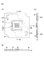
- FIGS. 7A to 7C are a top view and a cross-sectional view of the light emitting device 1.
- FIG. 2 is an enlarged cross-sectional view of the light emitting device 1.
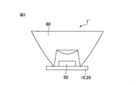
- FIG. 2 is a side view of a light emitting device 1 ′ with a lens 80.
- FIG. It is a graph which shows the relationship between the mounting space
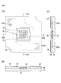
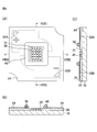
- FIGS. 7A to 7C are a top view and a cross-sectional view showing a manufacturing process of the light emitting device 1.
- FIGS. 7A to 7C are a top view and a cross-sectional view showing a manufacturing process of the light emitting device 1.
- FIGS. 7A to 7C are a top view and a cross-sectional view showing a manufacturing process of the light emitting device 1.
- FIGS. 7A to 7C are a top view and a cross-sectional view showing a manufacturing process of the light emitting device 1.
- (A) to (C) are a top view and a cross-sectional view of the light emitting device 2.
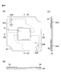
- FIGS. 4A to 4C are a top view and a cross-sectional view showing a manufacturing process of the light emitting device 2.
- FIGS. 4A to 4C are a top view and a cross-sectional view showing a manufacturing process of the light emitting device 2.
- FIGS. 4A to 4C are a top view and a cross-sectional view showing a manufacturing process of the light emitting device 2.
- FIGS. 4A to 4C are a top view and a cross-sectional view showing a manufacturing process of the light emitting device 2.
- FIGS. 4A to 4C are a top view and
- 1A to 1C are a top view and a cross-sectional view of the light-emitting device 1.
- 1A is a top view of the light-emitting device 1 as a finished product
- FIG. 1B is a cross-sectional view taken along line IB-IB in FIG. 1A
- FIG. 1C is FIG. It is sectional drawing along the IC-IC line of A).
- the light emitting device 1 includes an LED element as a light emitting element, and is used as various lighting devices such as an illumination LED and an LED bulb.
- the light emitting device 1 includes a mounting substrate 10, a circuit substrate 20, an LED element 30, a resin frame 40, a sealing resin 50, and a Zener diode 70 as main components.
- the mounting substrate 10 is a metal substrate having a substantially square shape as an example, and having a mounting region in which the LED element 30 is mounted at the center of the upper surface thereof. Since the mounting substrate 10 also functions as a heat dissipation substrate that dissipates heat generated by the LED elements 30 and phosphor particles described later, the mounting substrate 10 is made of aluminum having excellent heat resistance and heat dissipation, for example. However, as long as the material of the mounting substrate 10 is excellent in heat resistance and heat dissipation, another metal such as copper may be used.
- the circuit board 20 has a substantially square shape having the same size as the mounting board 10 and has a rectangular opening 21 at the center thereof.
- the lower surface of the circuit board 20 is fixed on the mounting board 10 by an adhesive sheet, for example.
- connection electrodes 23A and 23B for connecting the light emitting device 1 to an external power source are formed at two corners located diagonally on the upper surface of the circuit board 20.
- the connection electrode 23A is a positive electrode
- the connection electrode 23B is a negative electrode. When these are connected to an external power source and a voltage is applied, the light emitting device 1 emits light.
- a white resist 24 is formed on the upper surface of the circuit board 20 to cover the wiring patterns 22A and 22B except for the outer peripheral portion of the opening 21 and the portions of the connection electrodes 23A and 23B (FIG. 5A described later). See).
- the LED element 30 is an example of a light emitting element, and is, for example, a blue LED that emits blue light having an emission wavelength band of about 450 to 460 nm.
- the lateral width of the LED element 30 is, for example, about 500 to 600 ⁇ m.
- a plurality of LED elements 30 are mounted in a lattice pattern at the center of the mounting substrate 10 exposed in the opening 21 of the circuit board 20.
- FIG. 1A shows an example where 16 LED elements 30 are mounted.
- the LED element 30 is fixed to the upper surface of the mounting substrate 10 with, for example, a transparent insulating adhesive so that the light emitting surface is on the upper side (the side opposite to the mounting substrate 10).
- the LED element 30 has a pair of element electrodes on the upper surface, and the element electrodes of the adjacent LED elements 30 are electrically connected to each other by wires 31 as shown in FIG.
- the wires 31 coming out of the LED elements 30 located on the outer peripheral side of the opening 21 are connected to the wiring patterns 22 ⁇ / b> A and 22 ⁇ / b> B of the circuit board 20. Thereby, a current is supplied to each LED element 30 via the wire 31.
- the resin frame 40 is a substantially rectangular frame made of, for example, white resin in accordance with the size of the opening 21 of the circuit board 20, and is fixed to the outer peripheral portion of the opening 21 on the upper surface of the circuit board 20. .
- the resin frame 40 is a dam material for preventing the sealing resin 50 from flowing out, and the light emitted from the LED element 30 to the side is mounted above the light emitting device 1 (as viewed from the LED element 30). The light is reflected toward the opposite side of the substrate 10.
- the mounting area on the mounting substrate 10, the opening 21 of the circuit board 20, and the resin frame 40 are rectangular, but these may be other shapes such as a circle.
- the sealing resin 50 is injected into the opening 21 to expose the exposed portions of the plurality of LED elements 30 (for example, the upper surface of the LED elements 30 or the side surface of the LED element 30 mounted on the outermost side on the resin frame 40 side). ) Thereby, the sealing resin 50 integrally covers and protects (seals) the plurality of LED elements 30 and the wires 31.
- a colorless and transparent resin such as an epoxy resin or a silicone resin, particularly a resin having a heat resistance of about 250 ° C. may be used.
- a phosphor such as a yellow phosphor (a phosphor 51 in FIG. 2 described later) is dispersed and mixed in the sealing resin 50.
- the yellow phosphor is a particulate phosphor material such as YAG (yttrium aluminum garnet) that absorbs blue light emitted from the LED element 30 and converts the wavelength into yellow light.
- the light emitting device 1 emits white light obtained by mixing blue light from the LED element 30 which is a blue LED and yellow light obtained by exciting the yellow phosphor thereby.
- the sealing resin 50 may contain a plurality of types of phosphors such as a green phosphor and a red phosphor.
- the green phosphor is a particulate phosphor material such as (BaSr) 2 SiO 4 : Eu 2+ that absorbs blue light emitted from the LED element 30 and converts the wavelength into green light.
- the red phosphor is a particulate phosphor material such as CaAlSiN 3 : Eu 2+ that absorbs blue light emitted from the LED element 30 and converts the wavelength into red light.
- the light emitting device 1 is obtained by mixing blue light from the LED element 30 that is a blue LED and green light and red light obtained by exciting the green phosphor and the red phosphor thereby. Emits light.
- the phosphor in the sealing resin 50 is deposited on the upper surface of the LED element 30 and the upper surface of the mounting substrate 10 around the LED element 30 by natural sedimentation. That is, the sealing resin 50 contains the phosphor excited by the light from the LED element 30 at a higher concentration as it goes downward in the layer of the sealing resin 50.
- the heat generated in the LED element 30 and the phosphor easily escapes outside the device via the mounting substrate 10. Become. Accordingly, it is possible to prevent a decrease in the light emission intensity of the LED element 30 due to heat, which is advantageous in improving the light emission intensity.
- the zener diode 70 is provided on the circuit board 20 to prevent the LED element 30 from being destroyed by static electricity or the like.
- the Zener diode 70 is connected to the wiring patterns 22A and 22B in parallel with the plurality of LED elements 30 (see FIG. 7A described later), and bypasses current when a voltage is applied to the LED elements 30 in the reverse direction. Thus, the LED element 30 is protected.
- the plurality of LED elements 30 are densely arranged on the mounting substrate 10 so that the distance between adjacent LED elements 30 is 5 ⁇ m or more and 120% or less of the average particle diameter of the phosphor.
- An average particle diameter here is a median diameter, for example, refers to the median diameter D50.
- the particle diameter of the phosphor particles has a distribution over a certain range, and the median diameter D50 is a diameter in which the number of particles on the larger and smaller sides is equal when the particle size distribution of a certain particle is divided into two. That is.
- the phosphor those having an average particle diameter of 20 ⁇ m to 25 ⁇ m are widely used.
- a phosphor within this range may be used as the phosphor contained in the sealing resin 50.
- 120% of the average particle diameter is about 25 to 30 ⁇ m.
- a phosphor having a median diameter D50 of 25 ⁇ m is used, and a plurality of LED elements 30 are mounted at intervals of 30 ⁇ m.
- the sealing resin 50 contains a plurality of types of phosphors
- the plurality of LED elements 30 have an interval between adjacent LED elements 30 of 5 ⁇ m or more, and an average particle diameter among the plurality of types of phosphors. It is mounted so that the length is 120% or less of the median diameter D50 of the phosphor having the largest (median diameter D50).
- the spacing between the LED elements 30 may be 30 ⁇ m or more, but preferably at most 60 ⁇ m.
- the sealing resin 50 may contain a yellow phosphor having an average particle diameter of 25 ⁇ m, a green phosphor having an average particle diameter of 25 ⁇ m, and a red phosphor having an average particle diameter of 15 ⁇ m.
- FIG. 2 is an enlarged cross-sectional view of the light emitting device 1.
- the phosphor 51 contained in the sealing resin 50 is also illustrated.
- Reference numeral 60 denotes a space from the lower end to the upper end of each LED element 30 between the plurality of LED elements 30. Hereinafter, this space is referred to as “inter-element region 60”.
- the phosphor 51 is deposited on the upper surface of the mounting substrate 10 in the upper surface of the LED element 30, just above the inter-element region 60, and in the outer peripheral portion 52 between the inner wall of the opening 21 and the LED element 30 positioned on the outer peripheral side. Yes.
- the interval between the LED elements 30 is slightly larger than the average particle diameter of the phosphor 51, small phosphor particles have entered the inter-element region 60 to some extent.
- the interval between the LED elements 30 is set to 120% or less of the average particle diameter of the phosphor 51, the upper end of the inter-element region 60 is blocked with large phosphor particles as indicated by reference numeral 61 in FIG. Clogged.
- the sealing resin 50 may enter the inter-element region 60 or air bubbles may remain, but the phosphor 51 substantially does not enter when the upper end is blocked. For this reason, the phosphor 51 exists above the upper surface of the LED element 30.
- the phosphor 51 which is a yellow phosphor, longer than the emitted light, and is emitted to the outside of the light emitting device, so that the intensity of the yellow light is increased. That is, since the intensity of the yellow light varies depending on the position and direction of emission from the LED element 30, the color of the emitted light deviates from the design value.
- the concentration of the phosphor 51 in the inter-element region 60 is sealed on the upper side of the LED element 30. It is lower than the concentration of the phosphor 51 in the resin 50. For this reason, the light emission of the phosphor 51 in the inter-element region 60 is much weaker than the light emission of the phosphor 51 on the upper side of the LED element 30. The color change hardly occurs until the LED element 30 is passed through the upper side of the LED element 30.
- the emitted light from the upper surface of the LED element 30 and the emitted light from the side surface are emitted to the outside through the phosphor 51 layer by the same distance on the upper side of the LED element 30.
- the distance through which the emitted light passes through the phosphor layer is constant regardless of the emission position from 30 and the emission direction. Therefore, in the light emitting device 1, the light emitted from the LED element 30 to the side does not cause a variation in color, and a shift between the actual color of the emitted light and the color of the target light is less likely to occur. Therefore, outgoing light with uniform chromaticity can be obtained.
- each LED element 30 is mounted so that the light emitting surface of each LED element 30 is on the upper side. Therefore, even if a part of the phosphor is deposited in the inter-element region 60, The body is relatively far from the light emitting surface of each LED element 30. For this reason, even if the phosphor entering the inter-element region 60 is excited, it does not affect the variation in color of the emitted light (color unevenness).
- FIG. 2 shows a state where a large number of particles of the phosphor 51 have entered the outer peripheral portion 52 between the inner wall of the opening 21 and the LED element 30 located on the outer peripheral side. If the phosphor 51 is precipitated and the phosphor 51 can be disposed in the outer peripheral portion 52 with a thickness substantially equal to the upper side of the LED element 30, the particles of the phosphor 51 are present in the outer peripheral portion 52 unlike the inter-element region 60. There may be many. However, the width of the outer peripheral portion 52 is preferably narrower than the lateral width of the LED element 30, and preferably wider than the height of the circuit board 20.
- the width of the outer peripheral portion 52 is preferably about 200 to 400 ⁇ m.
- the height of the circuit board 20 is preferably the same as the height of the LED elements 30 or about 10% lower than that.
- the outer peripheral portion 52 may be closed by filling with a transparent resin or white resin not containing the phosphor.
- FIG. 3 is a side view of the light emitting device 1 ′ with the lens 80.
- the lens 80 is placed on the upper surface of the circuit board 20 so as to cover the sealing resin 50, for example.
- the lens 80 is an example of an optical element, condenses the light emitted from the plurality of LED elements 30 in the light emitting device 1, and emits the light above the light emitting device 1 '.
- a plurality of LED elements 30 are densely mounted and the light emitting portion (light emitting area) can be narrowed without reducing the number of elements, so that the light emitted from the LED elements 30 can be efficiently applied to the lens 80. It becomes possible to make it enter.
- an optical element other than the lens 80 such as a filter, may be placed on the circuit board 20.
- the light from the plurality of LED elements 30 in the light emitting device 1 may be emitted through a plate-shaped optical element instead of the lens 80.
- FIG. 4 is a graph showing the relationship between the mounting interval between the LED elements 30 and the illuminance of the light emitting device 1 ′.
- the horizontal axis of the graph is the mounting interval d ( ⁇ m) between the LED elements 30, and the vertical axis is the relative illuminance I based on the illuminance of the emitted light from the light emitting device 1 ′ when the mounting interval d is 0 mm.
- Each LED element 30 is a 1 mm square rectangle, and the incident end of the lens 80 is a circle having a diameter of 10 mm.
- the minimum value of the relative intensity I is 20 when the mounting distance d is 30 ⁇ m and when the mounting distance d is 50 ⁇ m, compared to when the mounting distance d is 0 ⁇ m, due to the variation in incorporation of the lens 80. It has decreased by about%.
- the maximum value and the average value of the relative strength I are almost constant regardless of the mounting interval d in the illustrated range.
- the mounting distance d between the LED elements 30 is so narrow that the light emitting point becomes smaller in order to collect light with the lens 80.
- a mounting interval d of at least about 5 ⁇ m so that a short circuit does not occur between adjacent LED elements 30, for example.
- the mounting interval d is excessively widened, the light emission diameter of the plurality of LED elements 30 with respect to the diameter of the incident end of the lens 80 is increased, resulting in light loss. Therefore, the illuminance of light emitted from the light emitting device 1 ′ is descend.
- the upper limit of the mounting interval d is preferably about 50 ⁇ m.
- the mounting interval of the LED elements 30 is not necessarily narrower than the particle diameter of the phosphor, and may be any length that is 120% or less of the average particle diameter of the phosphor.
- the LED elements 30 are densely packed as the mounting interval between the adjacent LED elements 30 is 5 ⁇ m or more and the phosphor (when the plural kinds of phosphors are used, the average particle diameter is the largest).
- the length is 120% or less of the median diameter D50.
- the mounting interval of the LED elements 30 is 30 ⁇ m corresponding to 120% of the average particle diameter of the phosphor particles. It has been confirmed that there is substantially no variation in the color of the emitted light if it is below.
- FIGS. 5A to 8C are a top view and a cross-sectional view showing a manufacturing process of the light emitting device 1.
- the mounting substrate 10 and the circuit substrate 20 having the opening 21 are overlaid and bonded together.
- 6 (A) to 6 (C) the light emitting surface is directed to the upper surface of the mounting board 10 exposed in the opening 21 of the circuit board 20 and the side opposite to the mounting board 10.
- a plurality of LED elements 30 are mounted.
- the interval between adjacent LED elements 30 is 5 ⁇ m or more, and the median diameter D50 of the phosphor used (the average particle diameter is the maximum when a plurality of types of phosphors are used) is used.
- the length should be 120% or less.
- the Zener diode 70 is also mounted between the wiring pattern 22A and the wiring pattern 22B on the upper surface of the circuit board 20.
- the adjacent LED elements 30 are electrically connected to each other by the wire 31, and the wire coming out of the LED element 30 on the outer peripheral side of the opening portion 21 is connected.
- 31 is connected to the wiring patterns 22A and 22B.
- the Zener diode 70 is also connected to the wiring patterns 22A and 22B by the wire 71.
- the resin frame 40 is fixed to the outer peripheral portion of the opening 21 on the upper surface of the circuit board 20.
- the whole of the plurality of LED elements 30 is sealed with a sealing resin 50 containing a phosphor.
- the phosphor is naturally settled in the sealing resin 50 while keeping the sealing resin 50 in an uncured state and is deposited on the upper surface of the LED element 30, and then the sealing resin 50 is cured.
- the light-emitting device 1 shown in FIGS. 1A to 1C is completed.
- FIG. 9A to 9C are a top view and a cross-sectional view of the light-emitting device 2.
- FIG. 9A is a top view of the light-emitting device 2 as a finished product
- FIG. 9B is a cross-sectional view taken along line IXB-IXB in FIG. 9A
- FIG. 9C is FIG.
- FIG. 6 is a cross-sectional view taken along line IXC-IXC of A).
- the light emitting device 2 includes a mounting substrate 10 ′, an LED element 30, a resin frame 40, a sealing resin 50, and a Zener diode 70 as main components.
- the light emitting device 2 is different from the light emitting device 1 in that there is no circuit board 20 having the opening 21 that is in the light emitting device 1.
- the mounting substrate 10 ′ is an insulating substrate made of ceramics, for example, and has a mounting region in which the LED element 30 is mounted at the center of the upper surface thereof.
- the same plurality of LED elements 30 as in the light emitting device 1 are mounted in a grid pattern at the center of the mounting substrate 10 ′.
- the + electrode side wiring pattern 22A and the ⁇ electrode side wiring pattern 22B are formed on the upper surface of the mounting substrate 10 ′.
- Connection electrodes 23A and 23B are formed at the two corners located at.
- a white resist 24 covering the wiring patterns 22A and 22B is formed on the upper surface of the mounting substrate 10 ′ except for the outer peripheral portion of the mounting region of the LED element 30 and the connection electrodes 23A and 23B (described later). (See FIG. 10A).
- the resin frame 40 is a substantially rectangular frame similar to that of the light-emitting device 1 made of, for example, white resin in accordance with the size of the mounting area of the mounting substrate 10 ′. However, the resin frame 40 may have another shape such as a circle.
- the sealing resin 50 is injected into a portion surrounded by the resin frame 40 on the mounting substrate 10 ′ to integrally cover and protect (seal) the whole of the plurality of LED elements 30.
- the sealing resin 50 is a resin having heat resistance, such as a silicone resin, in which a phosphor is dispersed and mixed, as in the light emitting device 1.
- the Zener diode 70 is connected to the wiring patterns 22A and 22B in parallel with the plurality of LED elements 30 on the mounting substrate 10 ′ (see FIG. 12A described later), and a voltage is applied to the LED element 30 in the reverse direction. The LED element 30 is protected when it is received.
- the plurality of LED elements 30 have a median diameter of a phosphor (the average particle diameter is the maximum when a plurality of kinds of phosphors are used) with an interval between adjacent LED elements 30 of 5 ⁇ m or more. It is mounted densely on the mounting substrate 10 so as to have a length of 120% or less of D50. Thereby, since the phosphor in the sealing resin 50 does not substantially enter the inter-element region 60, the distance that the emitted light passes through the phosphor layer is constant regardless of the emission position and the emission direction from the LED element 30. become. For this reason, also in the light-emitting device 2, the shift
- the inter-element region 60 may be provided as long as the phosphor can be arranged with a thickness substantially equal to the upper side of the LED element 30 in the outer peripheral portion between the resin frame 40 and the LED element 30 positioned on the outer peripheral side. Unlike the case, many particles of the phosphor 51 may enter. However, the width of the outer peripheral portion is preferably narrower than the lateral width of the LED element 30. Alternatively, the outer peripheral portion may be filled with a transparent resin or a white resin.
- an optical element such as the lens 80 similar to the light emitting device 1 ′ may be placed on the upper surface of the mounting substrate 10 ′ so as to cover the sealing resin 50.
- FIGS. 10A to 13C are a top view and a cross-sectional view showing a manufacturing process of the light emitting device 2.
- a mounting substrate 10 ′ on which wiring patterns 22A and 22B, connection electrodes 23A and 23B, and a white resist 24 are formed as shown in FIGS. 10A to 10C is prepared. Is done. Then, as shown in FIGS. 11A to 11C, a plurality of LED elements 30 are mounted in the center of the mounting substrate 10 ′ with the light emitting surface facing away from the mounting substrate 10. At this time, the interval between adjacent LED elements 30 is 5 ⁇ m or more, and the median diameter D50 of the phosphor used (the average particle diameter is the maximum when a plurality of types of phosphors are used) is used. The length should be 120% or less. At this time, the Zener diode 70 is also mounted between the wiring pattern 22A and the wiring pattern 22B on the upper surface of the mounting substrate 10 '.
- the adjacent LED elements 30 are electrically connected to each other by the wire 31, and the wire 31 coming out from the LED element 30 on the outer peripheral side of the mounting region is used.
- the wire 31 coming out from the LED element 30 on the outer peripheral side of the mounting region is used.
- the Zener diode 70 is also connected to the wiring patterns 22A and 22B by the wire 71.
- the resin frame 40 is fixed to the outer peripheral portion of the mounting region of the mounting substrate 10 '. Then, the whole of the plurality of LED elements 30 is sealed with a sealing resin 50 containing a phosphor. At that time, the phosphor is naturally settled in the sealing resin 50 while keeping the sealing resin 50 in an uncured state and is deposited on the upper surface of the LED element 30, and then the sealing resin 50 is cured.
- the light-emitting device 2 shown in FIGS. 9A to 9C is completed.
- the LED elements 30 are mounted by wire bonding, but the above configuration can be similarly applied to a light emitting device in which the LED elements are flip-chip mounted.
- the interval between a plurality of LED elements densely mounted on a mounting substrate and flip-chip mounted is set to the median of the phosphor used (the average particle diameter is the maximum when a plurality of types of phosphors are used).
- the length may be 120% or less of the diameter D50.
Landscapes
- Led Device Packages (AREA)
Abstract
Description
Claims (4)
- 基板と、
発光面を前記基板とは反対側に向けて、前記基板上に密集して実装された複数の発光素子と、
前記複数の発光素子からの光により励起される複数種類の蛍光体を前記複数の発光素子の上面に堆積した状態で含有し、前記複数の発光素子の全体を封止する封止樹脂と、を有し、
隣接する前記発光素子同士の間隔は、5μm以上であり、かつ前記複数種類の蛍光体のうちで平均粒径が最大である蛍光体のメジアン径D50の120%以下の長さである、
ことを特徴とする発光装置。 - 前記メジアン径D50は20μm以上かつ25μm以下である、請求項1に記載の発光装置。
- 前記封止樹脂を覆うように前記基板上に載置された光学素子をさらに有する、請求項1または2に記載の発光装置。
- 発光面を基板とは反対側に向けて、前記基板上に密集して複数の発光素子を実装する工程と、
前記複数の発光素子からの光により励起される複数種類の蛍光体を含有する封止樹脂で前記複数の発光素子の全体を封止する工程と、
前記複数種類の蛍光体を前記封止樹脂内で自然沈降させ、前記複数の発光素子の上面に堆積させてから前記封止樹脂を硬化させる工程と、を有し、
前記実装する工程では、隣接する発光素子同士の間隔が5μm以上でありかつ前記複数種類の蛍光体のうちで平均粒径が最大である蛍光体のメジアン径D50の120%以下の長さになるように、前記複数の発光素子を実装する、
ことを特徴とする発光装置の製造方法。
Priority Applications (3)
| Application Number | Priority Date | Filing Date | Title |
|---|---|---|---|
| CN201680031129.6A CN107615496A (zh) | 2015-05-29 | 2016-05-30 | 发光装置及其制造方法 |
| US15/577,714 US10629786B2 (en) | 2015-05-29 | 2016-05-30 | Light emitting device and manufacturing method thereof |
| JP2017521938A JP6700265B2 (ja) | 2015-05-29 | 2016-05-30 | 発光装置およびその製造方法 |
Applications Claiming Priority (4)
| Application Number | Priority Date | Filing Date | Title |
|---|---|---|---|
| JP2015110489 | 2015-05-29 | ||
| JP2015-110489 | 2015-05-29 | ||
| JPPCT/JP2016/053839 | 2016-02-09 | ||
| PCT/JP2016/053839 WO2016194405A1 (ja) | 2015-05-29 | 2016-02-09 | 発光装置およびその製造方法 |
Publications (1)
| Publication Number | Publication Date |
|---|---|
| WO2016194876A1 true WO2016194876A1 (ja) | 2016-12-08 |
Family
ID=57440235
Family Applications (1)
| Application Number | Title | Priority Date | Filing Date |
|---|---|---|---|
| PCT/JP2016/065931 Ceased WO2016194876A1 (ja) | 2015-05-29 | 2016-05-30 | 発光装置およびその製造方法 |
Country Status (1)
| Country | Link |
|---|---|
| WO (1) | WO2016194876A1 (ja) |
Cited By (1)
| Publication number | Priority date | Publication date | Assignee | Title |
|---|---|---|---|---|
| JP2020188044A (ja) * | 2019-05-10 | 2020-11-19 | 国立研究開発法人物質・材料研究機構 | 発光装置 |
Citations (3)
| Publication number | Priority date | Publication date | Assignee | Title |
|---|---|---|---|---|
| WO2012091008A1 (ja) * | 2010-12-28 | 2012-07-05 | 日亜化学工業株式会社 | 半導体発光装置 |
| JP2013153134A (ja) * | 2011-12-26 | 2013-08-08 | Nichia Chem Ind Ltd | 発光装置の製造方法 |
| JP2014027156A (ja) * | 2012-07-27 | 2014-02-06 | Citizen Holdings Co Ltd | Ledパッケージ |
-
2016
- 2016-05-30 WO PCT/JP2016/065931 patent/WO2016194876A1/ja not_active Ceased
Patent Citations (3)
| Publication number | Priority date | Publication date | Assignee | Title |
|---|---|---|---|---|
| WO2012091008A1 (ja) * | 2010-12-28 | 2012-07-05 | 日亜化学工業株式会社 | 半導体発光装置 |
| JP2013153134A (ja) * | 2011-12-26 | 2013-08-08 | Nichia Chem Ind Ltd | 発光装置の製造方法 |
| JP2014027156A (ja) * | 2012-07-27 | 2014-02-06 | Citizen Holdings Co Ltd | Ledパッケージ |
Cited By (4)
| Publication number | Priority date | Publication date | Assignee | Title |
|---|---|---|---|---|
| JP2020188044A (ja) * | 2019-05-10 | 2020-11-19 | 国立研究開発法人物質・材料研究機構 | 発光装置 |
| JP7226789B2 (ja) | 2019-05-10 | 2023-02-21 | 国立研究開発法人物質・材料研究機構 | 発光装置 |
| JP2024022662A (ja) * | 2019-05-10 | 2024-02-16 | 国立研究開発法人物質・材料研究機構 | 近赤外発光蛍光体および発光装置 |
| JP7773231B2 (ja) | 2019-05-10 | 2025-11-19 | 国立研究開発法人物質・材料研究機構 | 近赤外発光蛍光体および発光装置 |
Similar Documents
| Publication | Publication Date | Title |
|---|---|---|
| US10043954B2 (en) | Lighting device with a phosphor layer on a peripheral side surface of a light-emitting element and a reflecting layer on an upper surface of the light-emitting element and on an upper surface of the phosphor layer | |
| JP6567050B2 (ja) | 発光装置およびその製造方法 | |
| JP6387954B2 (ja) | 波長変換部材を用いた発光装置の製造方法 | |
| US10361344B2 (en) | Light emitting device | |
| JP6813599B2 (ja) | Ledパッケージおよびその製造方法 | |
| JP6700265B2 (ja) | 発光装置およびその製造方法 | |
| US10429050B2 (en) | Light-emitting apparatus having different packaging densities | |
| JP6643910B2 (ja) | 発光装置 | |
| TW201429005A (zh) | 具有齊納(zener)二極體上之整合式反射遮罩的發光二極體封裝 | |
| US20160079217A1 (en) | Semiconductor light emitting device and lead frame | |
| CN103797596A (zh) | 发光模块 | |
| JP6653119B2 (ja) | 半導体発光装置及びリードフレーム | |
| JP6566791B2 (ja) | 発光装置 | |
| JPWO2017134994A1 (ja) | 発光装置およびその製造方法 | |
| KR101518459B1 (ko) | Led 패키지 | |
| JP7161990B2 (ja) | 発光装置 | |
| JP2018022859A (ja) | 発光装置及びその製造方法 | |
| JP7444718B2 (ja) | 発光装置 | |
| JP2022015703A (ja) | 発光装置 | |
| JP7476002B2 (ja) | 発光装置 | |
| JP2019087695A (ja) | 発光装置 | |
| JP2015060995A (ja) | 発光装置 | |
| JP2020119994A (ja) | 発光装置及び発光装置の製造方法 |
Legal Events
| Date | Code | Title | Description |
|---|---|---|---|
| 121 | Ep: the epo has been informed by wipo that ep was designated in this application |
Ref document number: 16803311 Country of ref document: EP Kind code of ref document: A1 |
|
| ENP | Entry into the national phase |
Ref document number: 2017521938 Country of ref document: JP Kind code of ref document: A |
|
| WWE | Wipo information: entry into national phase |
Ref document number: 15577714 Country of ref document: US |
|
| NENP | Non-entry into the national phase |
Ref country code: DE |
|
| 122 | Ep: pct application non-entry in european phase |
Ref document number: 16803311 Country of ref document: EP Kind code of ref document: A1 |