WO2016190115A1 - 固体撮像素子およびその駆動方法、並びに電子機器 - Google Patents
固体撮像素子およびその駆動方法、並びに電子機器 Download PDFInfo
- Publication number
- WO2016190115A1 WO2016190115A1 PCT/JP2016/064085 JP2016064085W WO2016190115A1 WO 2016190115 A1 WO2016190115 A1 WO 2016190115A1 JP 2016064085 W JP2016064085 W JP 2016064085W WO 2016190115 A1 WO2016190115 A1 WO 2016190115A1
- Authority
- WO
- WIPO (PCT)
- Prior art keywords
- shutter
- pixel array
- electronic shutter
- pixel
- signal
- Prior art date
- Legal status (The legal status is an assumption and is not a legal conclusion. Google has not performed a legal analysis and makes no representation as to the accuracy of the status listed.)
- Ceased
Links
Images






Classifications
-
- H—ELECTRICITY
- H04—ELECTRIC COMMUNICATION TECHNIQUE
- H04N—PICTORIAL COMMUNICATION, e.g. TELEVISION
- H04N25/00—Circuitry of solid-state image sensors [SSIS]; Control thereof
- H04N25/50—Control of the SSIS exposure
- H04N25/53—Control of the integration time
- H04N25/532—Control of the integration time by controlling global shutters in CMOS SSIS
-
- H—ELECTRICITY
- H04—ELECTRIC COMMUNICATION TECHNIQUE
- H04N—PICTORIAL COMMUNICATION, e.g. TELEVISION
- H04N25/00—Circuitry of solid-state image sensors [SSIS]; Control thereof
- H04N25/70—SSIS architectures; Circuits associated therewith
- H04N25/76—Addressed sensors, e.g. MOS or CMOS sensors
-
- H—ELECTRICITY
- H04—ELECTRIC COMMUNICATION TECHNIQUE
- H04N—PICTORIAL COMMUNICATION, e.g. TELEVISION
- H04N25/00—Circuitry of solid-state image sensors [SSIS]; Control thereof
- H04N25/70—SSIS architectures; Circuits associated therewith
- H04N25/76—Addressed sensors, e.g. MOS or CMOS sensors
- H04N25/779—Circuitry for scanning or addressing the pixel array
Definitions
- the present technology relates to a solid-state imaging device, a driving method thereof, and an electronic device, and more particularly, to a solid-state imaging device capable of performing an electronic shutter at a higher speed, a driving method thereof, and an electronic device.
- shutters of imaging devices represented by digital still cameras and the like, there are a mechanical shutter (hereinafter referred to as a mechanical shutter) and a shutter controlled by turning on and off an image sensor (hereinafter referred to as an electronic shutter).
- a mechanical shutter hereinafter referred to as a mechanical shutter
- an electronic shutter a shutter controlled by turning on and off an image sensor
- the front curtain is an electronic shutter and the rear curtain is a mechanical shutter.
- the mechanical shutter is physically driven by a spring because it is driven by a spring, and its operation has a high-order curve characteristic.
- the electronic shutter drives the shutter by sequentially specifying addresses (rolling shutter), its operation has a linear characteristic.
- both the front curtain and the rear curtain are mechanical shutters
- the characteristics of the front curtain and the rear curtain are equal.
- the front curtain is an electronic shutter
- the rear curtain is a mechanical shutter
- the respective characteristics are different as described above, so that a phenomenon occurs in which the exposure time varies depending on the row.
- Patent Document 1 proposes a method for approximating the characteristics of an electronic shutter to the characteristics of a mechanical shutter.
- the technique disclosed in Patent Document 1 since a plurality of lines are simultaneously shuttered, the difference from the mechanical shutter characteristics becomes large.
- Patent Document 2 proposes control using a latch.
- Patent Document 2 has a limit in speeding up the electronic shutter.
- the present technology has been made in view of such a situation, and makes it possible to perform an electronic shutter at a higher speed.
- the solid-state imaging device controls a pixel array unit in which a plurality of pixels are arranged in a matrix and accumulation of signal charges in the pixels provided in row units of the pixel array unit.
- a drive circuit for outputting a drive signal for driving the pixel transistor; and a plurality of shutter control signals for decoding the address information and outputting a shutter control signal for controlling the electronic shutter to the drive circuit in the row of the pixel array unit corresponding to the decoded result A plurality of decoders, wherein the plurality of decoders output the shutter control signal in a time-sharing manner to the drive circuits provided in units of rows of the pixel array unit.
- the solid-state imaging device driving method includes a pixel array unit in which a plurality of pixels are arranged in a matrix, and accumulation of signal charges in the pixels provided in row units of the pixel array unit.
- a drive circuit that outputs a drive signal that drives a pixel transistor that controls the pixel, and decodes address information, and outputs a shutter control signal that controls the electronic shutter to the drive circuit in the row of the pixel array unit corresponding to the decoding result
- the plurality of decoders of the solid-state imaging device including a plurality of decoders that output the shutter control signal in a time-division manner to the drive circuit provided for each row of the pixel array unit.
- An electronic device includes a pixel array unit in which a plurality of pixels are arranged in a matrix, and a pixel that is provided in a row unit of the pixel array unit and controls accumulation of signal charges in the pixel
- a driving circuit for outputting a driving signal for driving a transistor
- a plurality of decoders for decoding address information and outputting a shutter control signal for controlling an electronic shutter to the driving circuit in the row of the pixel array unit corresponding to the decoding result
- the plurality of decoders include a solid-state imaging device that outputs the shutter control signal in a time-sharing manner to the drive circuit provided in a row unit of the pixel array unit.
- a shutter control signal is output in a time-sharing manner from a plurality of decoders to a drive circuit provided for each row of the pixel array unit.
- the solid-state imaging device and the electronic device may be independent devices or modules incorporated in other devices.
- the electronic shutter can be performed at higher speed.
- FIG. 7 is a block diagram illustrating a detailed configuration example of the driver in FIG. 6. It is a figure explaining operation
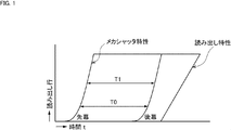
- FIG. 1 shows operating characteristics when both the front curtain and the rear curtain are configured with mechanical shutters.
- the mechanical shutter Since the mechanical shutter is driven by a spring, it is physically accelerating, and its operation is a high-order curve operation as shown in FIG.
- the characteristics of both are equal, and therefore the exposure time is equal in every row. That is, the exposure time T0 for a certain row is the same as the exposure time T1 for the other rows.
- the read operation of the signal charge accumulated by exposure has a linear characteristic as shown in FIG.
- FIG. 2 shows operating characteristics when the front curtain is an electronic shutter and the rear curtain is a mechanical shutter.
- the electronic shutter sequentially drives addresses by specifying addresses (rolling shutter)
- its characteristics are linear as in the read operation. Therefore, when the front curtain is an electronic shutter and the rear curtain is a mechanical shutter, the exposure time varies depending on the line as shown in FIG. That is, the exposure time T0 of a certain row is different from the exposure time T1 of another row.
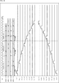
- the exposure time is equal for each row. Therefore, in order to eliminate the exposure time difference between the rows when the electronic shutter is used for the front curtain and the mechanical shutter is used for the rear curtain, the electronic shutter is combined with a plurality of linear characteristics as shown in FIG. There is a control method that operates by approximating the polygonal line.
- the mechanical shutter is not a type in which one plate is operated from one direction but an up-and-down type in which two plates are operated in the vertical direction.
- the electronic front curtain shutter is also shown in FIG.
- a non-linear operation is performed by approximating the polygonal line so as to be vertically symmetrical.
- the CMOS image sensor described below performs a driving operation to drive the electronic front curtain shutter by approximating the operating characteristics of the mechanical shutter with a broken line as shown in FIGS.
- the electronic front curtain shutter is also simply referred to as an electronic shutter.
- FIG. 5 is a diagram illustrating a schematic configuration example of a CMOS image sensor as a solid-state imaging device to which the present technology is applied.
- the CMOS image sensor 1 shown in FIG. 5 includes a pixel array unit 2, a vertical scanning circuit 3, a column CDS circuit 4, a horizontal scanning circuit 5, an output circuit 6, a timing generation circuit 7, and a control circuit 8.
- a plurality of pixels 20 are arranged in a matrix along the horizontal direction and the vertical direction.
- predetermined four adjacent rows in the pixel array unit 2 are shown as n rows, n + 1 rows, n + 2 rows, n + 3 rows (n> 0).
- the pixel array unit 2 has a photoelectric conversion unit 21 made of a photodiode and a transfer transistor 22 for each pixel, and a reset transistor 23, an amplification transistor 24, a selection transistor 25, and an FD (floating diffusion) 26 are vertically connected. It has the structure shared by the two pixels 20 adjacent in the direction.
- one pixel 20 is indicated by a pixel 20A
- the other pixel 20 is indicated by a pixel 20B.
- the photoelectric conversion unit 21 and the transfer transistor 22 of the pixel 20A are represented by a photoelectric conversion unit 21A and a transfer transistor 22A
- the photoelectric conversion unit 21 and the transfer transistor 22 of the pixel 20B are represented by a photoelectric conversion unit 21B and a transfer transistor 22B.
- the transfer transistors 22A and 22B, the reset transistor 23, the amplification transistor 24, and the selection transistor 25 are collectively referred to as pixel transistors.
- the present technology can be applied even when a pixel transistor independent for each pixel is used, or when three or more pixels share each pixel transistor except the transfer transistor.
- the transfer transistor 22A reads the signal charge of the photoelectric conversion unit 21A to the FD 26.
- the transfer transistor 22B reads the signal charge of the photoelectric conversion unit 21B to the FD 26.
- the reset transistor 23 resets the signal charge accumulated in the FD 26.
- the amplification transistor 24 generates a pixel signal corresponding to the potential of the FD 26.
- the selection transistor 25 selects a pixel that outputs a pixel signal.
- the sources of the corresponding transfer transistors 22A and 22B are connected to the output ends (cathodes) of the photoelectric conversion units 21A and 21B, respectively.
- Transfer lines 31A and 31B are connected to the gates of the transfer transistors 22A and 22B, respectively.
- the drains of the transfer transistors 22A and 22B are connected in common and connected to the reset transistor 23.
- the FD 26 between the drains of the transfer transistors 22 A and 22 B and the source of the reset transistor 23 is connected to the gate of the amplification transistor 24.
- the drain of the reset transistor 23 and the drain of the amplification transistor 24 are connected to the power line 32.
- the gate of the reset transistor 23 is connected to the reset line 33.
- the source of the amplification transistor 24 is connected to the drain of the selection transistor 25.
- the gate of the selection transistor 25 is connected to the selection line 34, and the source of the selection transistor 25 is connected to the vertical signal line 35.
- the vertical scanning circuit 3 selects each pixel 20 of the pixel array unit 2 in units of rows and reads out signal charges from the pixels 20 in units of rows. In other words, the vertical scanning circuit 3 controls each pixel 20 by selecting each pixel 20 of the pixel array unit 2 in units of rows.
- the column CDS circuit 4 takes in each pixel signal of the pixel array unit 2 in units of rows and performs CDS processing and other signal processing.
- the horizontal scanning circuit 5 scans the column CDS circuit 4 in the horizontal direction. In other words, the horizontal scanning circuit 5 performs signal processing for each column on the pixel signals read out by the vertical scanning circuit 3 in units of rows.
- the output circuit 6 performs necessary signal processing on the pixel signal transferred from the column CDS circuit 4 and outputs it as an image signal.
- the timing generation circuit 7 generates a control signal that synchronizes the operation timings of the vertical scanning circuit 3, the column CDS circuit 4, and the horizontal scanning circuit 5, and supplies the control signal to each circuit.
- the control circuit 8 receives an input clock and data for instructing an operation mode and outputs data such as internal information of the CMOS image sensor 1.
- the CMOS image sensor 1 configured as described above operates in a non-linear manner by controlling the electronic shutter (electronic front curtain shutter) as shown in FIGS. 3 and 4 by approximating the operating characteristics of the mechanical shutter with a broken line. be able to.
- the drive control of the electronic shutter performed by the CMOS image sensor 1 will be described in detail.
- FIG. 6 is a diagram illustrating a detailed configuration example of the vertical scanning circuit 3 together with the pixel array unit 2 and the timing generation circuit 7.
- the vertical scanning circuit 3 includes four decoders 41 and a driver 42, and controls an electronic shutter for the pixels 20 in each row of the pixel array unit 2.
- decoder 41 In FIG. 6, four decoders 41 are shown separately from the decoder 41A, the decoder 41B, the decoder 41C, and the decoder 41D. For four rows of n rows, n + 1 rows, n + 2 rows, and n + 3 rows. A case where the electronic shutter is controlled will be described. The description common to the decoders 41A to 41D will be described as the decoder 41.
- the timing generation circuit 7 starts counting with the timing pulse signal as a trigger, and generates address information ADR of the pixel 20 that performs the operation of the electronic shutter with m bits. Specifically, the timing generation circuit 7 uses ADR0 ⁇ 11: 0>, ADR1 ⁇ 11: 0>, ADR2 ⁇ 11: 0>, ADR3 ⁇ 11: 0 as address information ADR supplied to each of the decoders 41A to 41D. Generate>.
- the timing generation circuit 7 supplies the address information ADR0 ⁇ 11: 0> for n rows to the decoder 41A together with the shutter control signal I_txn for n rows. Further, the timing generation circuit 7 supplies the address information ADR1 ⁇ 11: 0> for the n + 1 row to the decoder 41B together with the shutter control signal I_txn + 1 for the n + 1 row. Similarly, the timing generation circuit 7 supplies the address information ADR2 ⁇ 11: 0> and the shutter control signal I_txn + 2 for the n + 2 row to the decoder 41C, and the address information ADR3 ⁇ 11: 0> and the shutter control signal I_txn for the n + 3 row. +3 is supplied to the decoder 41D.
- timing generation circuit 7 generates a latch set signal Sn and a latch reset signal Rn and supplies them to the driver 42 of the vertical scanning circuit 3.
- the decoder 41 decodes the address information ADR supplied from the timing generation circuit 7 and identifies the row of the pixel array unit 2 from the decoding result.
- the decoder 41 outputs the shutter control signal I_tx to the transfer signal generation circuit 60 (FIG. 8) in the driver 42 corresponding to the control target row obtained as a result of decoding.
- the decoder 41A since the address information ADR0 ⁇ 11: 0> specifies n rows, the decoder 41A outputs the shutter control signal I_txn to the transfer signal generation circuit 60 in the n rows in the driver 42.
- the decoder 41B outputs a shutter control signal I_txn + 1 to the transfer signal generation circuit 60 in the (n + 1) th row in the driver 42.
- the decoder 41C outputs the shutter control signal I_txn + 2 to the n + 2 row transfer signal generation circuit 60 in the driver 42
- the decoder 41D outputs the shutter control signal to the n + 3 row transfer signal generation circuit 60 in the driver 42.
- the four decoders 41A to 41D are switched in a time division manner and output the shutter control signal I_tx to the transfer signal generation circuit 60 in the driver 42.
- the driver 42 generates the transfer signal Tx based on the latch set signal Sn and latch reset signal Rn supplied from the timing generation circuit 7 and the shutter control signal I_tx supplied from the decoder 41, and the pixel array unit The transfer transistor 22 of each of the two pixels 20 is driven.
- the generation of the transfer signal Tx will be described later with reference to FIGS.
- the driver 42 also generates a reset signal RET for driving the reset transistor 23 of the pixel array unit 2 and a selection signal SEL for driving the selection transistor 25 and supplies the generated signal to each pixel 20 of the pixel array unit 2.
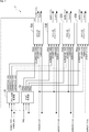
- FIG. 7 shows a detailed configuration example of a part of the timing generation circuit 7, specifically, a part related to generation of the address information ADR ⁇ 11: 0> and the shutter control signal I_tx.
- the timing generation circuit 7 includes an address width generation unit 51, a trigger generation unit 52, and four counters 53.
- the four counters 53 correspond to the decoders 41A to 41D of FIG. 6, and will be described as being distinguished as counters 53A to 53D as necessary.
- the counter 53A is a master counter
- the counters 53B to 53D are slave counters.
- the address width generation unit 51 uses the counters 53A through 53A based on the electronic shutter speed setting SPEED ⁇ 14: 0> supplied from the control circuit 8 and the parallel number setting PARA ⁇ 2: 0> indicating the address count-up number. Address widths ADRWDTH0 ⁇ 14: 0>, ADRWDTH1 ⁇ 14: 0>, ADRWDTH2 ⁇ 14: 0>, and ADRWDTH3 ⁇ 14: 0> to be supplied to 53D are generated. ⁇ 14: 0> indicates that the address width ADRWDTH is expressed by 15 bits from 0 to 14. Similarly, the parallel number setting PARA is represented by 3 bits from 0 to 2.
- a start address STADR ⁇ 11: 0>, offset values ADROF1 ⁇ 11: 0>, ADROF2 ⁇ 11: 0>, and ADROF3 ⁇ 11: 0>, which will be described later, are represented by 12 bits from 0 to 11. It shows that.
- the address width generator 51 carries out a polygonal line approximation of the electronic shutter based on the address width ADRWDTH0 ⁇ 14: 0> of the counter 53A, which is a master counter, so that the carry signal CO (Carry Out supplied from the counter 53A is used. ) To retiming.
- the trigger generation unit 52 generates trigger signals TRG0 to TRG3 based on the timing signal TRG, the electronic shutter speed setting SPEED ⁇ 14: 0>, and the parallel number setting PARA ⁇ 2: 0> supplied from the control circuit 8. Generated and supplied to the counters 53A to 53D.
- the counter 53A which is a master counter, generates address information ADR0 based on the address generation start signal TRG0, the address width ADRWDTH0 ⁇ 14: 0>, the start address STADR ⁇ 11: 0>, and the parallel number setting PARA ⁇ 2: 0>. ⁇ 11: 0> and a shutter control signal I_txn are generated.
- the generated address information ADR0 ⁇ 11: 0> and shutter control signal I_txn are supplied to the decoder 41A of the vertical scanning circuit 3 as described with reference to FIG.
- the start address STADR ⁇ 11: 0> is an address serving as a reference for the counters 53A to 53D.
- the counter 53B which is a slave counter, has an address generation start signal TRG1, an address width ADRWDTH1 ⁇ 14: 0>, a start address STADR ⁇ 11: 0>, a parallel number setting PARA ⁇ 2: 0>, and an offset value ADROF1 ⁇ 11: Based on 0>, address information ADR1 ⁇ 11: 0> and a shutter control signal I_txn + 1 are generated.
- the offset value ADROF1 ⁇ 11: 0> represents an offset value with respect to the address generated by the master counter.
- the generated address information ADR1 ⁇ 11: 0> and shutter control signal I_txn + 1 are supplied to the decoder 41B of the vertical scanning circuit 3.
- the counter 53C has an address generation start signal TRG2, an address width ADRWDTH2 ⁇ 14: 0>, a start address STADR ⁇ 11: 0>, a parallel number setting PARA ⁇ 2: 0>, and an offset value ADROF2 ⁇ 11: 0>. Based on this, address information ADR2 ⁇ 11: 0> and a shutter control signal I_txn + 2 are generated. The generated address information ADR2 ⁇ 11: 0> and shutter control signal I_txn + 2 are supplied to the decoder 41C of the vertical scanning circuit 3.
- the counter 53D has an address generation start signal TRG3, an address width ADRWDTH3 ⁇ 14: 0>, a start address STADR ⁇ 11: 0>, a parallel number setting PARA ⁇ 2: 0>, and an offset value ADROF3 ⁇ 11: 0>.
- address information ADR3 ⁇ 11: 0> and a shutter control signal I_txn + 3 are generated.
- the generated address information ADR3 ⁇ 11: 0> and shutter control signal I_txn + 3 are supplied to the decoder 41D of the vertical scanning circuit 3.
- the start address STADR ⁇ 11: 0>, offset value ADROF1 ⁇ 11: 0>, offset value ADROF2 ⁇ 11: 0>, and offset value ADROF3 ⁇ 11: 0> are supplied from the control circuit 8.
- FIG. 8 is a block diagram showing a detailed configuration example of the driver 42 shown in FIG.
- the driver 42 includes a transfer signal generation circuit 60 in units of transfer lines 31, in other words, in units of rows. In FIG. 8, a transfer signal generation circuit 60 corresponding to n rows is shown.
- the transfer signal generation circuit 60 is a drive circuit that drives a pixel transistor that controls accumulation of signal charges in each pixel 20 in a corresponding row in the pixel array unit 2, and generates and outputs a transfer signal Tx as a drive signal. To do.
- the transfer signal generation circuit 60 includes a latch 62, a first OR gate 64, and a second OR gate 66.
- the latch 62 has a positive logic set input terminal 62A, a positive logic reset input terminal 62B, and a negative logic output terminal 62C.
- FIG. 9 is an explanatory diagram showing the relationship between the set signal S input to the set input terminal 62A, the reset signal R input to the reset input terminal 62B, and the output signal Q bar of the output terminal 62C.
- the latch 62 holds the output signal Q bar at “0” when the set signal S becomes “1”, and sets the output signal Q bar at “1” when the reset signal R becomes “1”. ”.
- the latch 62 holds the output signal Q bar at “Low” when the set signal S is supplied, and holds the output signal Q bar at “Hi” when the reset signal R is supplied.
- Such a latch 62 corresponds to a memory that holds 1-bit data.
- a positive logic shutter control signal I_txn and a positive logic latch set signal Sn are input from the timing generation circuit 7 to the first OR gate 64.
- the output terminal of the first OR gate 64 is connected to the set input terminal 62A of the latch 62. Therefore, the logical sum of the shutter control signal I_txn and the latch set signal Sn is supplied to the set input terminal 62A of the latch 62.
- the second OR gate 66 receives the shutter control signal I_txn and the output signal Q bar of the output terminal 62C of the latch 62.
- the output signal Q bar is referred to as a latch output signal M_txn.
- the second OR gate 66 outputs the logical sum of the shutter control signal I_txn and the latch output signal M_txn as the transfer signal Txn.
- the transfer signal generation circuit 60 of FIG. 8 has a latch 62 that is set by the logical sum of the shutter control signal I_txn and the latch set signal Sn, and reset by the latch reset signal Rn.
- the signal M_txn is output.
- the transfer signal Txn output from the transfer signal generation circuit 60 is configured by a logical sum of the shutter control signal I_txn and the latch output signal M_txn.
- the reset signal RST supplied to each reset transistor 23 of the pixel array unit 2 is fixed to “Hi” as shown in FIG.
- the timing generation circuit 7 fixes the latch set signal Sn to “Low” as shown in FIG. 10 and outputs the shutter control signals I_txn, I_txn + 1, I_txn + 2, I_txn + 3,.
- a “Hi” pulse signal is simultaneously supplied to each transfer signal generation circuit 60 as the latch reset signal Rn.
- the transfer signal generation circuit 60 supplies each pixel 20 with the reset signal RST set to the valid state and the transfer signals Txn, Txn + 1, Txn + 2, Txn + 3,. As a result, all the pixels in the pixel array unit 2 are reset simultaneously.
- the decoder 41 outputs the shutter control signal I_tx to the transfer signal generation circuit 60 in the driver 42 corresponding to the control target row obtained as a result of decoding the address information ADR. Specifically, as shown in FIG. 10, the decoder 41 generates “Hi” pulse signals as respective transfer control signals as respective shutter control signals I_txn, I_txn + 1, I_txn + 2, I_txn + 3,. The signals are sequentially output to the circuit 60.
- the pulse width ⁇ X of each shutter control signal I_txn, I_txn + 1, I_txn + 2, I_txn + 3,... Is the same, and the time point when the shutter control signal that precedes in time falls This coincides with the time when the shutter control signal rises.
- the shutter control signals I_txn, I_txn + 1, I_txn are performed. +2, I_txn + 3, ... are fixed to "Low”. Then, by setting the latch set signal Sn to “Hi” at a predetermined timing, each transfer signal Txn, Txn + 1, Txn + 2, Txn + 3,... A global shutter operation can be realized.
- each shutter control signal I_tx is set to one clock width of the operation clock CK of the vertical scanning circuit 3, and each row of the pixel array unit 2 is sequentially set at one clock interval.
- the linear characteristics of the electronic shutter can be changed between when the signal charge accumulation period is started and when the signal charge accumulation period is sequentially started at intervals of two clocks.
- a parameter for setting the linear characteristic of the electronic shutter is the electronic shutter speed setting SPEED ⁇ 14: 0>.
- the electronic shutter speed setting SPEED ⁇ 14: 0> is set in two adjacent rows in the pixel array unit 2. This corresponds to the timing difference (time difference) at which the shutter control signal I_tx is supplied to the transfer signal generation circuit 60.
- the electronic shutter speed setting SPEED ⁇ 14: 0> is “1”
- the control circuit 8 of the CMOS image sensor 1 makes the pixel array unit 2 like a first pixel region 71, a second pixel region 72, and a third pixel region 73, for example.
- a different electronic shutter speed setting SPEED is set for each pixel area.
- control circuit 8 combines the plurality of linear characteristics by setting different electronic shutter speed settings SPEED for the plurality of pixel regions, and performs nonlinear operation by approximating the polygonal line, thereby operating the mechanical shutter.
- the electronic front curtain shutter can be operated in accordance with the characteristics.
- the pixel array unit 2 is divided into three pixel areas, but the number of divisions of the pixel areas is not limited to “3”.
- FIG. 13 shows a timing chart when the electronic shutter speed setting SPEED ⁇ 14: 0> is set to “1” and the electronic shutter operation is performed in four parallels using the four decoders 41.
- the decoder 41 of the vertical scanning circuit 3 takes a predetermined time until the address information ADR supplied from the timing generation circuit 7 is decoded and the pixel row of the pixel array unit 2 is specified.
- the frequency of the operation clock CK of the vertical scanning circuit 3 is determined based on one decoding processing time by the decoder 41.
- the frequency of the operation clock CK of the vertical scanning circuit 3 is set to be one decoding processing time in the decoder 41 when the same number as the number of the decoders 41 is counted.
- the frequency of the operation clock CK is set so that one decoding process time is equal to four clock times of the operation clock CK.
- the speed setting SPEED ⁇ 14: 0> of the electronic shutter is the fastest speed setting, that is, when the speed setting SPEED ⁇ 14: 0> of the electronic shutter is 1, equal time intervals (every clock time)
- the four decoders 41 can be processed in parallel.
- the address width generation unit 51 sets the multiplication result of the electronic shutter speed setting SPEED ⁇ 14: 0> and the parallel number setting PARA ⁇ 2: 0> to the address width ADRWDTH ⁇ 14: 0>.
- the address width ADRWDTH ⁇ 14: 0> that is, ADRWDTH0 ⁇ 14: 0>, ADRWDTH1 ⁇ 14: 0>, ADRWDTH2 ⁇ 14: 0>, and ADRWDTH3 ⁇ 14: 0> are as follows.
- TRG0 to TRG3 output by the trigger generation unit 52 are determined as follows using the timing signal TRG and the electronic shutter speed setting SPEED ⁇ 14: 0>.
- ⁇ i> is set as address information ADR0 ⁇ 11: 0> in the counter 53A which is a master counter.
- the address information ADR0 ⁇ 11: 0> ADR0 ⁇ i> in which ⁇ i> is set is output from the counter 53A to the decoder 41A together with the shutter control signal I_tx ⁇ i>.
- the counter 53B which is a slave counter, is supplied with “1” as the offset value ADROF1 ⁇ 11: 0>, and is offset into the address information ADR0 ⁇ i> of the counter 53A, which is the master counter, as address information ADR1 ⁇ 11: 0>.
- ⁇ I + 1> obtained by adding the value ADROF1 ⁇ 11: 0> is set.
- the address information ADR1 ⁇ 11: 0> ADR1 ⁇ i + 1> in which ⁇ i + 1> is set is output from the counter 53B to the decoder 41B together with the shutter control signal I_tx ⁇ i + 1>.
- “2” is supplied as the offset value ADROF1 ⁇ 11: 0> to the counter 53C, and the offset value is added to the address information ADR0 ⁇ i> of the counter 53A as the master counter as the address information ADR2 ⁇ 11: 0>.
- ⁇ I + 2> obtained by adding ADROF2 ⁇ 11: 0> is set.
- the address information ADR2 ⁇ 11: 0> ADR2 ⁇ i + 2> in which ⁇ i + 2> is set is output from the counter 53C to the decoder 41C together with the shutter control signal I_tx ⁇ i + 2>.
- FIG. 14 shows a timing chart in the case where the electronic shutter speed setting SPEED ⁇ 14: 0> is set to “2” and the electronic shutter operation is performed in four parallels using the four decoders 41.
- the address width ADRWDTH ⁇ 14: 0> generated by the address width generation unit 51 is determined as follows.
- TRG0 to TRG3 generated by the trigger generation unit 52 are determined as follows.
- ADR1 ⁇ i + 5> is output to the decoder 41B together with the shutter control signal I_tx ⁇ i + 5>.
- FIG. 15 shows a timing chart in the case where the speed setting SPEED ⁇ 14: 0> of the electronic shutter is changed to 3, 2, 1.
- the address width generation unit 51 sets the address width ADRWDTH ⁇ 14: 0> as follows.
- the electronic shutter speed setting SPEED ⁇ 14: 0> is changed from the first electronic shutter speed (“3” in the above example) to the second.
- the time interval for outputting the shutter control signal I_tx can be changed step by step in units of rows.
- the electronic shutter speed setting SPEED ⁇ 14: 0> can be switched smoothly.
- the mechanical shutter includes a vertical type that operates in the vertical direction using two plates.
- FIG. 16 is a timing chart showing an electronic shutter operation corresponding to such an up / down type mechanical shutter operation.
- the pixel array unit 2 (pixel region) is divided into two in the vertical direction, and two of the four decoders 41 are divided. The remaining two decoders 41 are used to control the other divided lower pixel region.
- the timing generation circuit 7 receives the address ⁇ j> input to the two decoders 41. Are controlled to be decremented one address at a time.
- the timing generation circuit 7 receives the address ⁇ i input to the two decoders 41 > Is controlled to be incremented by one address.
- FIG. 16 shows a timing chart in which the electronic shutter speed setting SPEED ⁇ 14: 0> is changed to 4, 3, and 2 in each of the divided upper pixel region and lower pixel region.
- the electronic shutter is controlled so that the upper pixel region and the lower pixel region obtained by dividing the pixel array unit 2 (pixel region) in the vertical direction are vertically symmetric. .
- the CMOS image sensor 1 includes an electronic shutter drive in which a single plate is operated from one direction as shown in FIG. 15 and approximated by a broken line to a one-side type mechanical shutter, and two plates as shown in FIG. It is possible to switch between an electronic shutter drive that approximates a polygonal line with an up-and-down type mechanical shutter that operates in a vertical direction by an operation setting mode.
- a control signal for controlling which electronic shutter drive is performed can be input from the outside of the CMOS image sensor 1.
- the CMOS image sensor 1 has the four decoders 41 in the vertical scanning circuit 3.
- the four decoders 41 operate in parallel, decode the address information ADR supplied from the timing generation circuit 7 (within the corresponding counter 53), and a transfer signal generation circuit provided for each row in the driver 42.
- the shutter control signal I_tx is output in a time-sharing manner.
- a predetermined time is required for the decoder 41 to decode the input address information ADR. Therefore, when the vertical scanning circuit 3 has only one decoder 41, the driver 42 is connected to the pixel array unit 2. The time from driving a certain row until the next row can be driven depends on the decoding processing time of the decoder 41.
- the vertical scanning circuit 3 has four decoders 41 and the four decoders 41 operate in parallel and output the shutter control signal I_tx in a time division manner as in the CMOS image sensor 1.
- the shutter control signal I_tx can be output to the driver 42 at a time interval of 1/4.
- each pixel 20 of the pixel array unit 2 can be driven at a higher speed than when only one decoder 41 is provided.
- the electronic shutter can be performed at higher speed, and an image with less distortion of the subject can be generated.
- the CMOS image sensor 1 divides the pixel array unit 2 into a plurality of pixel regions in the vertical direction, and sets the speed setting speed SPEED of the electronic shutter for each pixel region.
- the speed setting speed SPEED of the electronic shutter for each pixel region.
- the vertical scanning circuit 3 includes the four decoders 41
- the four decoders 41 operate in parallel, and outputs the shutter control signal I_tx in a time division manner. It is also possible to operate in parallel using only two of the four decoders 41.
- the number of decoders 41 provided in the vertical scanning circuit 3 is not limited to the above-described four, but may be other numbers, for example, two, eight, sixteen or the like.
- the CMOS image sensor 1 includes a plurality of decoders 41 in the vertical scanning circuit 3, a plurality of counters 53 corresponding to the plurality of decoders 41 in the timing generation circuit 7, and two of the plurality of decoders 41.
- the above decoder 41 can be operated in parallel, and the shutter control signal I_tx can be output to the driver 42 in a time division manner.
- the present technology is not limited to application to a solid-state imaging device. That is, the present technology is applied to an image capturing unit (photoelectric conversion unit) such as an imaging device such as a digital still camera or a video camera, a portable terminal device having an imaging function, or a copying machine using a solid-state imaging device as an image reading unit.
- the present invention can be applied to all electronic devices using a solid-state image sensor.
- the solid-state imaging device may be formed as a one-chip, or may be in a module shape having an imaging function in which an imaging unit and a signal processing unit or an optical system are packaged together.
- FIG. 17 is a block diagram illustrating a configuration example of an imaging apparatus as an electronic apparatus to which the present technology is applied.
- An imaging apparatus 100 in FIG. 17 includes an optical unit 101 including a lens group, a solid-state imaging device (imaging device) 102 in which the configuration of the solid-state imaging device 1 in FIG. 5 is employed, and a DSP (Digital Signal) that is a camera signal processing circuit. Processor) circuit 103 is provided.
- the imaging apparatus 100 also includes a frame memory 104, a display unit 105, a recording unit 106, an operation unit 107, and a power supply unit 108.
- the DSP circuit 103, the frame memory 104, the display unit 105, the recording unit 106, the operation unit 107, and the power supply unit 108 are connected to each other via a bus line 109.
- the optical unit 101 takes in incident light (image light) from a subject and forms an image on the imaging surface of the solid-state imaging device 102.
- the solid-state imaging device 102 converts the amount of incident light imaged on the imaging surface by the optical unit 101 into an electrical signal in units of pixels and outputs the electrical signal.
- the solid-state imaging device 102 the solid-state imaging device 1 of FIG. 5, that is, a solid-state that can drive an electronic shutter at high speed and can perform an electronic shutter operation having a characteristic approximated by a broken line to the operating characteristics of a mechanical shutter.
- An image sensor can be used.
- the display unit 105 includes a panel type display device such as a liquid crystal panel or an organic EL (Electro Luminescence) panel, and displays a moving image or a still image captured by the solid-state image sensor 102.
- the recording unit 106 records a moving image or a still image captured by the solid-state imaging device 102 on a recording medium such as a hard disk or a semiconductor memory.
- the operation unit 107 issues operation commands for various functions of the imaging apparatus 100 under the operation of the user.
- the power supply unit 108 appropriately supplies various power sources serving as operation power sources for the DSP circuit 103, the frame memory 104, the display unit 105, the recording unit 106, and the operation unit 107 to these supply targets.
- the electronic shutter can be operated at high speed by using the solid-state imaging device 1 according to the above-described embodiment as the solid-state imaging device 102, an image with less distortion of the subject can be generated. . Accordingly, even in the imaging apparatus 100 such as a video camera, a digital still camera, or a camera module for a mobile device such as a mobile phone, it is possible to improve the image quality of the captured image.
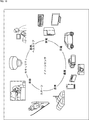
- FIG. 18 is a diagram showing a usage example in which the above CMOS image sensor 1 is used.
- CMOS image sensor 1 can be used in various cases for sensing light such as visible light, infrared light, ultraviolet light, and X-ray as follows.
- Devices for taking images for viewing such as digital cameras and mobile devices with camera functions
- Devices used for traffic such as in-vehicle sensors that capture the back, surroundings, and interiors of vehicles, surveillance cameras that monitor traveling vehicles and roads, and ranging sensors that measure distances between vehicles, etc.
- Equipment used for home appliances such as TVs, refrigerators, air conditioners, etc. to take pictures and operate the equipment according to the gestures ⁇ Endoscopes, equipment that performs blood vessel photography by receiving infrared light, etc.
- Equipment used for medical and health care ⁇ Security equipment such as security surveillance cameras and personal authentication cameras ⁇ Skin measuring instrument for photographing skin and scalp photography Such as a microscope to do beauty Equipment used for sports-Equipment used for sports such as action cameras and wearable cameras for sports applications-Used for agriculture such as cameras for monitoring the condition of fields and crops apparatus
- Embodiments of the present technology are not limited to the above-described embodiments, and various modifications can be made without departing from the gist of the present technology.
- this technique can also take the following structures.
- a pixel array section in which a plurality of pixels are arranged in a matrix;
- a driving circuit that outputs a driving signal for driving a pixel transistor that controls accumulation of signal charges in the pixel, provided in a row unit of the pixel array unit;
- a plurality of decoders for decoding address information and outputting a shutter control signal for controlling an electronic shutter to the drive circuit in the row of the pixel array unit corresponding to the decoding result;
- the plurality of decoders output the shutter control signal in a time-sharing manner to the drive circuit provided for each row of the pixel array unit.
- the solid-state imaging according to (1) further including a control circuit that sets an electronic shutter speed corresponding to a difference in timing when the shutter control signal is supplied to the drive circuits in two adjacent rows of the pixel array unit. element.
- the control circuit sets different electronic shutter speeds for each of a plurality of pixel regions obtained by dividing the pixel array unit in a vertical direction.
- the control circuit sets the electronic shutter speed for each of the plurality of pixel regions so as to have a characteristic approximated by a polygonal line to an operation characteristic of the mechanical shutter.
- the solid-state imaging device according to (3) or (4), wherein the control circuit sets the electronic shutter speed so as to be vertically symmetric with respect to the plurality of pixel regions with a vertical direction as a vertical direction.
- the control circuit changes an electronic shutter speed between the first electronic shutter speed and the second electronic shutter speed when the electronic shutter speed is switched from the first electronic shutter speed to the second electronic shutter speed.
- the solid-state imaging device according to any one of (3) to (5), wherein the first electronic shutter speed is switched to the second electronic shutter speed via the first electronic shutter speed.
- a pixel array section in which a plurality of pixels are arranged in a matrix;
- a driving circuit that outputs a driving signal for driving a pixel transistor that controls accumulation of signal charges in the pixel, provided in a row unit of the pixel array unit;
- a solid-state imaging device comprising: a plurality of decoders for decoding address information and outputting a shutter control signal for controlling an electronic shutter to the drive circuit in the row of the pixel array unit corresponding to the decoding result;
- a pixel array section in which a plurality of pixels are arranged in a matrix;
- a driving circuit that outputs a driving signal for driving a pixel transistor that controls accumulation of signal charges in the pixel, provided in a row unit of the pixel array unit;
- a plurality of decoders for decoding address information and outputting a shutter control signal for controlling an electronic shutter to the drive circuit in the row of the pixel array unit corresponding to the decoding result;
- the plurality of decoders is an electronic apparatus including a solid-state imaging device that outputs the shutter control signal in a time-sharing manner to the drive circuit provided for each row of the pixel array unit.
- 1 solid-state imaging device 2 pixel array unit, 3 vertical scanning circuit, 7 timing generation circuit, 8 control circuit, 20 pixels, 21 photoelectric conversion unit, 22 transfer transistor, 23 reset transistor, 41 decoder, 42 driver, 51 address width generation , 52 trigger generation unit, 53 counter, 60 transfer signal generation circuit, 100 imaging device, 102 solid-state imaging device
Landscapes
- Engineering & Computer Science (AREA)
- Multimedia (AREA)
- Signal Processing (AREA)
- Transforming Light Signals Into Electric Signals (AREA)
Abstract
本技術は、電子シャッタをより高速に行うことができるようにする固体撮像素子およびその駆動方法、並びに電子機器に関する。 固体撮像素子は、複数の画素が行列状に配置された画素アレイ部と、画素アレイ部の行単位に設けられた、画素における信号電荷の蓄積を制御する画素トランジスタを駆動する駆動信号を出力する駆動回路と、アドレス情報をデコードし、デコード結果に対応する画素アレイ部の行の駆動回路に、電子シャッタを制御するシャッタ制御信号を出力する複数のデコーダとを備える。複数のデコーダは、画素アレイ部の行単位に設けられた駆動回路に、シャッタ制御信号を時分割で出力する。本技術は、例えば、固体撮像素子等に適用できる。
Description
本技術は、固体撮像素子およびその駆動方法、並びに電子機器に関し、特に、電子シャッタをより高速に行うことができるようにする固体撮像素子およびその駆動方法、並びに電子機器に関する。
デジタルスチルカメラなどに代表される撮像装置のシャッタには、機械式のシャッタ(以下、メカシャッタと記述する)と、イメージセンサのオンオフで制御するシャッタ(以下、電子シャッタと記述する)がある。
また、近年の撮像装置では、先幕と後幕の2枚のシャッタ幕のうち、先幕を電子シャッタとし、後幕をメカシャッタとしたものがある。
メカシャッタは、バネによる駆動のため、物理的に加速度運動をしており、その動作は高次曲線的な特性となる。一方、電子シャッタは、順次アドレスを指定してシャッタを駆動していくため(ローリングシャッタ)、その動作は直線的な特性となる。
したがって、先幕と後幕のどちらもメカシャッタである場合には、先幕と後幕の特性が等しくなる。しかし、先幕を電子シャッタとし、後幕をメカシャッタとした場合には、上述したようにそれぞれの特性が異なるため、露光時間が行によって異なる現象が発生する。
そのため、例えば、特許文献1では、電子シャッタの特性を、メカシャッタの特性に近似させる方法が提案されている。しかし、特許文献1に開示されている技術では、複数行を同時にシャッタするため、メカシャッタ特性との差分が大きくなってしまう。
近年、高画素化に伴い、電子シャッタも高速化が求められている。電子シャッタの高速化を実現させるため、特許文献2に記載されている技術では、ラッチを用いた制御が提案されている。
しかしながら、特許文献2で提案されている技術では、電子シャッタの高速化に限界がある。
本技術は、このような状況に鑑みてなされたものであり、電子シャッタをより高速に行うことができるようにするものである。
本技術の第1の側面の固体撮像素子は、複数の画素が行列状に配置された画素アレイ部と、前記画素アレイ部の行単位に設けられた、前記画素における信号電荷の蓄積を制御する画素トランジスタを駆動する駆動信号を出力する駆動回路と、アドレス情報をデコードし、デコード結果に対応する前記画素アレイ部の行の前記駆動回路に、電子シャッタを制御するシャッタ制御信号を出力する複数のデコーダとを備え、前記複数のデコーダは、前記画素アレイ部の行単位に設けられた前記駆動回路に、前記シャッタ制御信号を時分割で出力する。
本技術の第2の側面の固体撮像素子の駆動方法は、複数の画素が行列状に配置された画素アレイ部と、前記画素アレイ部の行単位に設けられた、前記画素における信号電荷の蓄積を制御する画素トランジスタを駆動する駆動信号を出力する駆動回路と、アドレス情報をデコードし、デコード結果に対応する前記画素アレイ部の行の前記駆動回路に、電子シャッタを制御するシャッタ制御信号を出力する複数のデコーダとを備える固体撮像素子の、前記複数のデコーダが、前記画素アレイ部の行単位に設けられた前記駆動回路に、前記シャッタ制御信号を時分割で出力する。
本技術の第3の側面の電子機器は、複数の画素が行列状に配置された画素アレイ部と、前記画素アレイ部の行単位に設けられた、前記画素における信号電荷の蓄積を制御する画素トランジスタを駆動する駆動信号を出力する駆動回路と、アドレス情報をデコードし、デコード結果に対応する前記画素アレイ部の行の前記駆動回路に、電子シャッタを制御するシャッタ制御信号を出力する複数のデコーダとを備え、前記複数のデコーダは、前記画素アレイ部の行単位に設けられた前記駆動回路に、前記シャッタ制御信号を時分割で出力する固体撮像素子を備える。
本技術の第1乃至第3の側面においては、複数のデコーダから、画素アレイ部の行単位に設けられた駆動回路に、シャッタ制御信号が時分割で出力される。
固体撮像素子及び電子機器は、独立した装置であっても良いし、他の装置に組み込まれるモジュールであっても良い。
本技術の第1乃至第3の側面によれば、電子シャッタをより高速に行うことができる。
なお、ここに記載された効果は必ずしも限定されるものではなく、本開示中に記載されたいずれかの効果であってもよい。
以下、本技術を実施するための形態(以下、実施の形態という)について説明する。なお、説明は以下の順序で行う。
1.メカシャッタと電子シャッタの特性について
2.CMOSイメージセンサの構成説明
3.電子シャッタ動作説明
4.電子機器への適用例
1.メカシャッタと電子シャッタの特性について
2.CMOSイメージセンサの構成説明
3.電子シャッタ動作説明
4.電子機器への適用例
<1.メカシャッタと電子シャッタの特性について>
初めに、図1乃至図4を参照して、メカシャッタと電子シャッタの特性について説明する。
初めに、図1乃至図4を参照して、メカシャッタと電子シャッタの特性について説明する。
図1は、先幕と後幕の両方を、メカシャッタで構成した場合の動作特性を示している。
メカシャッタは、バネによる駆動のため、物理的に加速度運動をしており、その動作は、図1に示されるように高次曲線的な動作となる。先幕と後幕のどちらもメカシャッタとした場合には、両者の特性が等しくなるため、露光時間は、どの行においても等しくなる。すなわち、ある行の露光時間T0と、他の行の露光時間T1は同じになる。露光により蓄積された信号電荷の読み出し動作は、図1に示されるように、直線的な特性となる。
図2は、先幕を電子シャッタとし、後幕をメカシャッタとした場合の動作特性を示している。
電子シャッタは順次アドレスを指定してシャッタを駆動していくため(ローリングシャッタ)、その特性は、読み出し動作と同様に直線的な特性となる。したがって、先幕を電子シャッタとし、後幕をメカシャッタとした場合には、図2に示されるように、露光時間が行によって異なることになる。すなわち、ある行の露光時間T0と、他の行の露光時間T1が異なる。
露光時間は、行毎に等しいことが望ましい。そこで、先幕に電子シャッタを用いて、後幕にメカシャッタを用いた場合の各行の露光時間差をなくすため、電子シャッタを、図3で示すように、複数の線形特性を組み合わせ、メカシャッタの動作特性に折れ線近似させて動作させる制御方法がある。
なお、メカシャッタは、1枚の板を片方向から動作させるタイプではなく、2枚の板を上下方向に動作させる上下タイプもあり、この場合は、電子先幕シャッタも、図4に示されるように、上下対称となるように、折れ線近似させて非線形的に動作させる。
以下で説明するCMOSイメージセンサは、電子先幕シャッタの駆動制御を、図3及び図4に示したように、メカシャッタの動作特性に折れ線近似させて動作させる駆動を行う。なお、以下の説明では、電子先幕シャッタを、単に、電子シャッタともいう。
<2.CMOSイメージセンサの構成説明>
<2.1 概略構成例>
図5は、本技術を適用した固体撮像素子としてのCMOSイメージセンサの概略構成例を示す図である。
<2.1 概略構成例>
図5は、本技術を適用した固体撮像素子としてのCMOSイメージセンサの概略構成例を示す図である。
図5に示されるCMOSイメージセンサ1は、画素アレイ部2、垂直走査回路3、カラムCDS回路4、水平走査回路5、出力回路6、タイミング生成回路7、及び、制御回路8を有する。
画素アレイ部2には、複数の画素20が水平方向および垂直方向に沿って行列状に配置されている。
図5では、画素アレイ部2内の隣接する所定の4行を、n行、n+1行、n+2行、n+3行(n>0)として示している。
画素アレイ部2は、フォトダイオードからなる光電変換部21と転送トランジスタ22を画素単位に個別に有し、リセットトランジスタ23、増幅トランジスタ24、選択トランジスタ25、及び、FD(フローティングディフュージョン)26を、垂直方向において隣り合う2つの画素20で共有する構成を有している。
図5では、リセットトランジスタ23、増幅トランジスタ24、選択トランジスタ25、及び、FD26を共有する2つの画素20のうち、一方の画素20を画素20Aで示し、他方の画素20を画素20Bで示している。また、画素20Aの光電変換部21と転送トランジスタ22を、光電変換部21Aと転送トランジスタ22Aで表し、画素20Bの光電変換部21と転送トランジスタ22を、光電変換部21Bと転送トランジスタ22Bで表している。
なお、以下では、転送トランジスタ22A及び22B、リセットトランジスタ23、増幅トランジスタ24、並びに、選択トランジスタ25のそれぞれを、総称して画素トランジスタという。
本実施の形態では、上述したように、隣り合う2つの画素が、転送トランジスタを除く各画素トランジスタを共用する場合について説明する。しかしながら、本技術は、画素毎に独立した画素トランジスタを用いる場合であっても、あるいは、3個以上の画素が転送トランジスタを除く各画素トランジスタを共用する場合であっても適用可能である。
転送トランジスタ22Aは、光電変換部21Aの信号電荷をFD26に読み出す。転送トランジスタ22Bは、光電変換部21Bの信号電荷をFD26に読み出す。
リセットトランジスタ23は、FD26に蓄積された信号電荷をリセットする。増幅トランジスタ24は、FD26の電位に応じた画素信号を生成する。選択トランジスタ25は、画素信号を出力する画素を選択する。
光電変換部21A及び21Bの出力端(カソード)に対して、それぞれ対応する転送トランジスタ22A及び22Bのソースが接続されている。転送トランジスタ22A及び22Bのゲートには、転送線31A及び31Bが、それぞれ接続されている。
転送トランジスタ22A及び22Bのドレインは、共通接続されてリセットトランジスタ23に接続されている。転送トランジスタ22A及び22Bのドレインとリセットトランジスタ23のソースとの間のFD26は、増幅トランジスタ24のゲートに接続されている。
リセットトランジスタ23のドレイン及び増幅トランジスタ24のドレインは、電源線32に接続されている。リセットトランジスタ23のゲートは、リセット線33に接続されている。
増幅トランジスタ24のソースは、選択トランジスタ25のドレインに接続されている。選択トランジスタ25のゲートは、選択線34に接続され、選択トランジスタ25のソースが、垂直信号線35に接続されている。
垂直走査回路3は、画素アレイ部2の各画素20を行単位で選択して各画素20から行単位で信号電荷を読み出す。言い換えると、垂直走査回路3は、画素アレイ部2の各画素20を行単位で選択して各画素20の制御を行う。
カラムCDS回路4は、画素アレイ部2の各画素信号を行単位で取り込んでCDS処理やその他の信号処理を行う。
水平走査回路5は、カラムCDS回路4を水平方向に走査するものであり、言い換えると、垂直走査回路3によって行単位で読み出された画素信号に対して列ごとに信号処理を行う。
出力回路6は、カラムCDS回路4から転送される画素信号に必要な信号処理を施して画像信号として出力する。
タイミング生成回路7は、垂直走査回路3、カラムCDS回路4、水平走査回路5の動作タイミングを同期させる制御信号を生成し、各回路へ供給する。
制御回路8は、入力クロックと、動作モードなどを指令するデータを受け取り、またCMOSイメージセンサ1の内部情報などのデータを出力する。
以上のように構成されるCMOSイメージセンサ1は、電子シャッタ(電子先幕シャッタ)の制御を、図3及び図4に示したように、メカシャッタの動作特性に折れ線近似させて非線形的に動作させることができる。以下、CMOSイメージセンサ1が行う電子シャッタの駆動制御について詳細に説明する。
<2.2 垂直走査回路の詳細構成例>
図6は、画素アレイ部2とタイミング生成回路7とともに、垂直走査回路3の詳細構成例を示す図である。
図6は、画素アレイ部2とタイミング生成回路7とともに、垂直走査回路3の詳細構成例を示す図である。
垂直走査回路3は、4つのデコーダ41とドライバ42を含んで構成され、画素アレイ部2の各行の画素20に対して、電子シャッタの制御を行う。
図6では、4つのデコーダ41が、デコーダ41A、デコーダ41B、デコーダ41C、及び、デコーダ41Dと区別して示されており、n行、n+1行、n+2行、及び、n+3行の4行に対して電子シャッタの制御を行う場合について説明する。デコーダ41A乃至41Dに共通する説明については、デコーダ41として説明する。
タイミング生成回路7は、タイミングパルス信号をトリガにカウントを開始し、電子シャッタの動作を行う画素20のアドレス情報ADRをmビットで生成する。具体的には、タイミング生成回路7は、デコーダ41A乃至41Dそれぞれに供給するアドレス情報ADRとして、ADR0<11:0>, ADR1<11:0>, ADR2<11:0>, ADR3<11:0>を生成する。ここで、<11:0>は、アドレス情報ADRが、0乃至11までの12ビットで表されていることを示している。したがって、本実施の形態では、m=12であり、画素アレイ部2の行数が4096行まで対応可能となる。
タイミング生成回路7は、n行に対するアドレス情報ADR0<11:0>を、n行に対するシャッタ制御信号I_txnとともに、デコーダ41Aに供給する。また、タイミング生成回路7は、n+1行に対するアドレス情報ADR1<11:0>を、n+1行に対するシャッタ制御信号I_txn+1とともに、デコーダ41Bに供給する。同様に、タイミング生成回路7は、n+2行に対するアドレス情報ADR2<11:0>とシャッタ制御信号I_txn+2をデコーダ41Cに供給し、n+3行に対するアドレス情報ADR3<11:0>とシャッタ制御信号I_txn+3をデコーダ41Dに供給する。
また、タイミング生成回路7は、ラッチ用セット信号Snとラッチ用リセット信号Rnを生成し、垂直走査回路3のドライバ42へ供給する。
デコーダ41は、タイミング生成回路7から供給されるアドレス情報ADRをデコードし、デコード結果から、画素アレイ部2の行を特定する。デコーダ41は、デコードの結果得られた制御対象の行に対応する、ドライバ42内の転送信号生成回路60(図8)へ、シャッタ制御信号I_txを出力する。いまの場合、アドレス情報ADR0<11:0>はn行を特定しているので、デコーダ41Aは、ドライバ42内のn行の転送信号生成回路60へ、シャッタ制御信号I_txnを出力する。同様に、デコーダ41Bは、ドライバ42内のn+1行の転送信号生成回路60へ、シャッタ制御信号I_txn+1を出力する。同様に、デコーダ41Cは、ドライバ42内のn+2行の転送信号生成回路60へシャッタ制御信号I_txn+2を出力し、デコーダ41Dは、ドライバ42内のn+3行の転送信号生成回路60へシャッタ制御信号I_txn+3を出力する。換言すれば、4つのデコーダ41A乃至41Dは、時分割で切り替えて、ドライバ42内の転送信号生成回路60へシャッタ制御信号I_txを出力する。
ドライバ42は、タイミング生成回路7から供給されるラッチ用セット信号Snとラッチ用リセット信号Rn、及び、デコーダ41から供給されるシャッタ制御信号I_txに基づいて、転送信号Txを生成し、画素アレイ部2の各画素20の転送トランジスタ22を駆動する。転送信号Txの生成については、図8及び図9を参照して後述する。
また、ドライバ42は、画素アレイ部2のリセットトランジスタ23を駆動するリセット信号RET、及び、選択トランジスタ25を駆動する選択信号SELも生成し、画素アレイ部2の各画素20に供給する。
<2.3 タイミング生成回路の詳細構成例>
図7は、タイミング生成回路7の一部、具体的には、アドレス情報ADR<11:0>とシャッタ制御信号I_txの生成に関する部分の詳細構成例を示している。
図7は、タイミング生成回路7の一部、具体的には、アドレス情報ADR<11:0>とシャッタ制御信号I_txの生成に関する部分の詳細構成例を示している。
タイミング生成回路7は、アドレス幅生成部51及びトリガ生成部52と、4つのカウンタ53を含んで構成される。
4つのカウンタ53は、図6のデコーダ41A乃至41Dに対応するものであり、必要に応じてカウンタ53A乃至53Dとして区別して説明する。また、カウンタ53A乃至53Dのうち、カウンタ53Aがマスタカウンタであり、カウンタ53B乃至53Dがスレーブカウンタとなる。
アドレス幅生成部51は、制御回路8から供給される電子シャッタの速度設定SPEED<14:0>と、アドレスのカウントアップ数を示す並列数設定PARA<2:0>に基づいて、カウンタ53A乃至53Dに供給するアドレス幅ADRWDTH0<14:0>, ADRWDTH1<14:0>, ADRWDTH2<14:0>、及び、ADRWDTH3<14:0>を生成する。<14:0>は、アドレス幅ADRWDTHが0から14までの15ビットで表されていることを示している。同様に、並列数設定PARAは、0から2までの3ビットで表されている。後述する開始アドレスSTADR<11:0>やオフセット値ADROF1<11:0>,ADROF2<11:0>,ADROF3<11:0>も同様に、それらが0から11までの12ビットで表されていることを示している。
また、アドレス幅生成部51は、マスタカウンタであるカウンタ53Aのアドレス幅ADRWDTH0<14:0>を基準に、電子シャッタの折れ線近似を行うため、カウンタ53Aから供給される桁上げ信号CO(Carry Out)でリタイミングを行う。
トリガ生成部52は、制御回路8から供給されるタイミング信号TRG、電子シャッタの速度設定SPEED<14:0>、及び、並列数設定PARA<2:0>を基に、トリガ信号TRG0乃至TRG3を生成し、カウンタ53A乃至53Dに供給する。
マスタカウンタであるカウンタ53Aは、アドレス生成開始信号TRG0、アドレス幅ADRWDTH0<14:0>、開始アドレスSTADR<11:0>、及び、並列数設定PARA<2:0>を基に、アドレス情報ADR0<11:0>とシャッタ制御信号I_txnを生成する。生成されたアドレス情報ADR0<11:0>とシャッタ制御信号I_txnは、図6を参照して説明したように、垂直走査回路3のデコーダ41Aに供給される。開始アドレスSTADR<11:0>は、カウンタ53A乃至53Dの基準となるアドレスである。
スレーブカウンタであるカウンタ53Bは、アドレス生成開始信号TRG1、アドレス幅ADRWDTH1<14:0>、開始アドレスSTADR<11:0>、並列数設定PARA<2:0>、及び、オフセット値ADROF1<11:0>を基に、アドレス情報ADR1<11:0>とシャッタ制御信号I_txn+1を生成する。オフセット値ADROF1<11:0>は、マスタカウンタが生成するアドレスとのオフセット値を表す。生成されたアドレス情報ADR1<11:0>とシャッタ制御信号I_txn+1は、垂直走査回路3のデコーダ41Bに供給される。
カウンタ53Cも同様に、アドレス生成開始信号TRG2、アドレス幅ADRWDTH2<14:0>、開始アドレスSTADR<11:0>、並列数設定PARA<2:0>、及び、オフセット値ADROF2<11:0>を基に、アドレス情報ADR2<11:0>とシャッタ制御信号I_txn+2を生成する。生成されたアドレス情報ADR2<11:0>とシャッタ制御信号I_txn+2は、垂直走査回路3のデコーダ41Cに供給される。
カウンタ53Dも同様に、アドレス生成開始信号TRG3、アドレス幅ADRWDTH3<14:0>、開始アドレスSTADR<11:0>、並列数設定PARA<2:0>、及び、オフセット値ADROF3<11:0>を基に、アドレス情報ADR3<11:0>とシャッタ制御信号I_txn+3を生成する。生成されたアドレス情報ADR3<11:0>とシャッタ制御信号I_txn+3は、垂直走査回路3のデコーダ41Dに供給される。
開始アドレスSTADR<11:0>、オフセット値ADROF1<11:0>、オフセット値ADROF2<11:0>、及び、オフセット値ADROF3<11:0>は、制御回路8から供給される。
<2.4 ドライバの詳細構成例>
図8は、図6に示したドライバ42の詳細構成例を示すブロック図である。
図8は、図6に示したドライバ42の詳細構成例を示すブロック図である。
ドライバ42は、転送線31単位に、言い換えると、行単位に、転送信号生成回路60を備える。図8では、n行に対応する転送信号生成回路60が図示されている。
転送信号生成回路60は、画素アレイ部2内の対応する行の各画素20における信号電荷の蓄積を制御する画素トランジスタを駆動する駆動回路であり、駆動信号としての転送信号Txを生成して出力する。転送信号生成回路60は、ラッチ62、第1ORゲート64、及び、第2ORゲート66を含んで構成されている。
ラッチ62は、正論理のセット入力端子62Aと、正論理のリセット入力端子62Bと、負論理の出力端子62Cとを有している。
図9は、セット入力端子62Aに入力されるセット信号Sと、リセット入力端子62Bに入力されるリセット信号Rと、出力端子62Cの出力信号Qバーとの関係を示す説明図である。
図9に示すように、ラッチ62は、セット信号Sが「1」になると、出力信号Qバーを「0」に保持し、リセット信号Rが「1」になると、出力信号Qバーを「1」に保持する。
言い換えると、ラッチ62は、セット信号Sが供給されると出力信号Qバーを「Low」に保持し、リセット信号Rが供給されると出力信号Qバーを「Hi」に保持する。なお、このようなラッチ62は、1ビットのデータを保持するメモリに相当している。
言い換えると、ラッチ62は、セット信号Sが供給されると出力信号Qバーを「Low」に保持し、リセット信号Rが供給されると出力信号Qバーを「Hi」に保持する。なお、このようなラッチ62は、1ビットのデータを保持するメモリに相当している。
図8に戻り、第1ORゲート64には、タイミング生成回路7から、正論理のシャッタ制御信号I_txnと正論理のラッチ用セット信号Snとが入力される。
第1ORゲート64の出力端子は、ラッチ62のセット入力端子62Aに接続されている。したがって、ラッチ62のセット入力端子62Aには、シャッタ制御信号I_txnとラッチ用セット信号Snの論理和が供給される。
第2ORゲート66は、シャッタ制御信号I_txnと、ラッチ62の出力端子62Cの出力信号Qバーとが入力される。以下、説明の便宜上、出力信号Qバーをラッチ出力信号M_txnという。
第2ORゲート66は、シャッタ制御信号I_txnとラッチ出力信号M_txnとの論理和を転送信号Txnとして出力する。
したがって、図8の転送信号生成回路60は、シャッタ制御信号I_txnとラッチ用セット信号Snとの論理和によってセットされ、ラッチ用リセット信号Rnによってリセットされるラッチ62を有し、ラッチ62は、出力信号M_txnを出力する。転送信号生成回路60が出力する転送信号Txnは、シャッタ制御信号I_txnとラッチ出力信号M_txnとの論理和で構成される。
<3.電子シャッタ動作説明>
<3.1 ローリング電子シャッタ動作の説明>
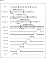
次に、図10を参照して、CMOSイメージセンサ1のローリング電子シャッタ動作について説明する。
<3.1 ローリング電子シャッタ動作の説明>
次に、図10を参照して、CMOSイメージセンサ1のローリング電子シャッタ動作について説明する。
なお、以下の説明では、信号レベルを正論理で説明するものとし、したがって、「Low」は「0」に対応し、「Hi」は「1」に対応している。
ローリング電子シャッタ動作では、画素アレイ部2の各リセットトランジスタ23に供給されるリセット信号RSTは、図10に示されるように、「Hi」に固定される。
タイミング生成回路7は、ラッチ用セット信号Snを、図10に示すように、「Low」に固定し、かつ、各シャッタ制御信号I_txn、I_txn+1、I_txn+2、I_txn+3、……を「Low」にした状態で、ラッチ用リセット信号Rnとして「Hi」のパルス信号を、各転送信号生成回路60に同時に供給する。
「Hi」のラッチ用リセット信号Rnにより、各転送信号生成回路60のラッチ出力信号M_txn、M_txn+1、M_txn+2、M_txn+3、……は、同時に「Hi」となり、さらに、各転送信号Txn、Txn+1、Txn+2、Txn+3、……も、同時に「Hi」となる。
これにより、画素アレイ部2の各行の各画素20の全てが同時にリセットされ、言い換えると、電子シャッタが掛けられたシャッタ期間が開始される。
すなわち、転送信号生成回路60は、有効状態としたリセット信号RSTと、有効状態とした転送信号Txn、Txn+1、Txn+2、Txn+3、……とを行単位で各画素20に供給することで画素アレイ部2の全画素を同時にリセットする。
次いで、デコーダ41は、アドレス情報ADRをデコードした結果得られた制御対象の行に対応する、ドライバ42内の転送信号生成回路60へ、シャッタ制御信号I_txを出力する。具体的には、デコーダ41は、図10に示すように、各シャッタ制御信号I_txn、I_txn+1、I_txn+2、I_txn+3、……として、「Hi」のパルス信号を、各転送信号生成回路60に順次出力する。
ここで、各シャッタ制御信号I_txn、I_txn+1、I_txn+2、I_txn+3、……のパルス幅△Xは同一であり、かつ、時間的に先行するシャッタ制御信号が立ち下る時点と、次のシャッタ制御信号が立ち上がる時点とは一致している。
図10に示すように、各シャッタ制御信号I_txn、I_txn+1、I_txn+2、I_txn+3、……が「Hi」に順次遷移することに応じて、各ラッチ出力信号M_txn、M_txn+1、M_txn+2、M_txn+3、……は、「Hi」から「Low」に順次遷移する。
さらに、各シャッタ制御信号I_txn、I_txn+1、I_txn+2、I_txn+3、……が「Low」に順次遷移することに応じて、転送信号Txn、Txn+1、Txn+2、Txn+3、……が、「Low」に順次遷移する。
これにより、各画素20のリセットが行単位で順次解除され、各画素20の光電変換部21における信号電荷の蓄積が開始される。言い換えると、「Hi」の転送信号Txが転送トランジスタ22に供給されていたシャッタ期間が終了し、信号電荷の蓄積期間が開始される。
なお、行単位に順次電子シャッタを行うローリング電子シャッタ動作ではなく、画素アレイ部2の全画素で同時に電子シャッタを行うグローバルシャッタ動作を行う場合には、各シャッタ制御信号I_txn、I_txn+1、I_txn+2、I_txn+3、……が、「Low」に固定設定される。そして、ラッチ用セット信号Snを所定のタイミングで「Hi」に設定することで、各転送信号Txn、Txn+1、Txn+2、Txn+3、……が一斉に「Low」に遷移し、グローバルシャッタ動作を実現することができる。
<3.2 折れ線近似制御の説明>
例えば、図11に示されるように、各シャッタ制御信号I_txのパルス幅△Xを、垂直走査回路3の動作クロックCKの1クロック幅として、画素アレイ部2の各行を、1クロック間隔で、順次、信号電荷の蓄積期間を開始させた場合と、2クロック間隔で、順次、信号電荷の蓄積期間を開始させた場合とで、電子シャッタの線形特性を変えることができる。
例えば、図11に示されるように、各シャッタ制御信号I_txのパルス幅△Xを、垂直走査回路3の動作クロックCKの1クロック幅として、画素アレイ部2の各行を、1クロック間隔で、順次、信号電荷の蓄積期間を開始させた場合と、2クロック間隔で、順次、信号電荷の蓄積期間を開始させた場合とで、電子シャッタの線形特性を変えることができる。
この電子シャッタの線形特性を設定するパラメータが、電子シャッタの速度設定SPEED<14:0>であり、電子シャッタの速度設定SPEED<14:0>は、画素アレイ部2内の隣接する2行の転送信号生成回路60にシャッタ制御信号I_txが供給されるタイミングの差分(時間差)に相当する。1クロック間隔で電子シャッタを順次動作させる場合、電子シャッタの速度設定SPEED<14:0>は「1」となり、2クロック間隔で電子シャッタを順次動作させる場合、電子シャッタの速度設定SPEED<14:0>は「2」となる。したがって、電子シャッタの速度設定SPEED<14:0>=1が、最速の電子シャッタ速度となる。
CMOSイメージセンサ1の制御回路8は、画素アレイ部2を、図12に示されるように、例えば、第1の画素領域71、第2の画素領域72、及び第3の画素領域73のように垂直方向に3分割し、各画素領域に対して、異なる電子シャッタの速度設定SPEEDを設定する。例えば、制御回路8は、第1の画素領域71を電子シャッタの速度設定SPEED<14:0>=3、第2の画素領域72を電子シャッタの速度設定SPEED<14:0>=2、第3の画素領域73を電子シャッタの速度設定SPEED<14:0>=1に設定する。
このように、制御回路8は、複数の画素領域に対して異なる電子シャッタの速度設定SPEEDを設定することにより複数の線形特性を組み合わせ、折れ線近似させて非線形的に動作させることにより、メカシャッタの動作特性に合わせた電子先幕シャッタの動作を行わせることができる。なお、図12の例では、画素アレイ部2を、3つの画素領域に分割したが、画素領域の分割数は、「3」に限定されるものではない。
<3.3 並列数設定PARA=4、電子シャッタ速度SPEED=1の例>
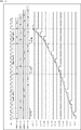
図13は、電子シャッタの速度設定SPEED<14:0>を「1」にして、4つのデコーダ41を用いて4並列で、電子シャッタ動作を行う場合のタイミングチャートを示している。
図13は、電子シャッタの速度設定SPEED<14:0>を「1」にして、4つのデコーダ41を用いて4並列で、電子シャッタ動作を行う場合のタイミングチャートを示している。
垂直走査回路3のデコーダ41は、タイミング生成回路7から供給されるアドレス情報ADRをデコードし、画素アレイ部2の画素行を特定するまで、所定の時間を要する。このデコーダ41による1回のデコード処理時間を基準として、垂直走査回路3の動作クロックCKの周波数が決定される。
具体的には、垂直走査回路3の動作クロックCKの周波数は、デコーダ41の個数と同じ数だけカウントされたとき、デコーダ41における1回のデコード処理時間となるように設定される。
本実施の形態では、デコーダ41の個数は4個であるので、1回のデコード処理時間が、動作クロックCKの4クロック時間と等しくなるように、動作クロックCKの周波数が設定される。
これにより、電子シャッタの速度設定SPEED<14:0>が最速の速度設定、即ち、電子シャッタの速度設定SPEED<14:0>=1のとき、等間隔時間で(1クロック時間ごとに)、各デコーダ41の開始タイミングをずらして、4つのデコーダ41を並列処理させることができる。
アドレス幅生成部51は、電子シャッタの速度設定SPEED<14:0>と並列数設定PARA<2:0>の乗算結果を、アドレス幅ADRWDTH<14:0>に設定する。アドレス幅ADRWDTH<14:0>、即ち、ADRWDTH0<14:0>, ADRWDTH1<14:0>, ADRWDTH2<14:0>, ADRWDTH3<14:0>のそれぞれは、以下のようになる。
ADRWDTH<14:0> = SPEED<14:0> x PARA<2:0>=1x4=4
ADRWDTH<14:0> = SPEED<14:0> x PARA<2:0>=1x4=4
トリガ生成部52が出力するトリガ信号TRG0乃至TRG3は、タイミング信号TRGと電子シャッタの速度設定SPEED<14:0>とを用いて、以下のように決定される。
TRG0=TRG
TRG1=TRG0 + SPEED<14:0>=TRG0 + 1
TRG2=TRG1 + SPEED<14:0>=TRG1 + 1
TRG3=TRG2 + SPEED<14:0>=TRG2 + 1
TRG0=TRG
TRG1=TRG0 + SPEED<14:0>=TRG0 + 1
TRG2=TRG1 + SPEED<14:0>=TRG1 + 1
TRG3=TRG2 + SPEED<14:0>=TRG2 + 1
開始アドレスSTADR<11:0>を<i>としたとき、マスタカウンタであるカウンタ53Aには、アドレス情報ADR0<11:0>として<i>がセットされる。そして、<i>がセットされたアドレス情報ADR0<11:0>=ADR0<i>が、シャッタ制御信号I_tx<i>とともに、カウンタ53Aからデコーダ41Aに出力される。カウンタ53Aは、アドレス幅ADRWDTH0<14:0>=4clock分カウントした後に、アドレス情報ADR0<i>を、PARA<2:0>=4だけカウントアップし、カウントアップ後のアドレス情報ADR0<i+4>を、次のアドレス情報ADR0<11:0>として、シャッタ制御信号I_tx<i+4>とともに出力する。
スレーブカウンタであるカウンタ53Bには、オフセット値ADROF1<11:0>として「1」が供給され、アドレス情報ADR1<11:0>として、マスタカウンタであるカウンタ53Aのアドレス情報ADR0<i>にオフセット値ADROF1<11:0>を加算した<i+1>がセットされる。そして、<i+1>がセットされたアドレス情報ADR1<11:0>=ADR1<i+1>が、シャッタ制御信号I_tx<i+1>とともに、カウンタ53Bからデコーダ41Bに出力される。カウンタ53Bは、アドレス幅ADRWDTH1<14:0>=4clock分カウントした後に、アドレス情報ADR1<i+1>を、PARA<2:0>=4だけカウントアップし、カウントアップ後のアドレス情報ADR1<i+5>を、次のアドレス情報ADR1<11:0>として、シャッタ制御信号I_tx<i+5>とともに出力する。
同様に、カウンタ53Cには、オフセット値ADROF1<11:0>として「2」が供給され、アドレス情報ADR2<11:0>として、マスタカウンタであるカウンタ53Aのアドレス情報ADR0<i>にオフセット値ADROF2<11:0>を加算した<i+2>がセットされる。そして、<i+2>がセットされたアドレス情報ADR2<11:0>=ADR2<i+2>が、シャッタ制御信号I_tx<i+2>とともに、カウンタ53Cからデコーダ41Cに出力される。カウンタ53Cは、アドレス幅ADRWDTH2<14:0>=4clock分カウントした後に、アドレス情報ADR2<i+2>を、PARA<2:0>=4だけカウントアップし、カウントアップ後のアドレス情報ADR2<i+6>を、次のアドレス情報ADR2<11:0>として、シャッタ制御信号I_tx<i+6>とともに出力する。
カウンタ53Dには、オフセット値ADROF2<11:0>として「3」が供給され、アドレス情報ADR3<11:0>として、マスタカウンタであるカウンタ53Aのアドレス情報ADR0<i>にオフセット値ADROF3<11:0>を加算した<i+3>がセットされる。そして、<i+3>がセットされたアドレス情報ADR3<11:0>=ADR3<i+3>が、シャッタ制御信号I_tx<i+3>とともに、カウンタ53Dからデコーダ41Dに出力される。カウンタ53Dは、アドレス幅ADRWDTH3<14:0>=4clock分カウントした後に、アドレス情報ADR3<i+3>を、PARA<2:0>=4だけカウントアップし、カウントアップ後のアドレス情報ADR3<i+7>を、次のアドレス情報ADR3<11:0>として、シャッタ制御信号I_tx<i+7>とともに出力する。
以上のようにカウンタ53A乃至53Dから出力されたシャッタ制御信号I_txn、I_txn+1、I_txn+2、I_txn+3、……を、開始アドレスSTADR<11:0>である<i>から順にみると、図13に示されるように、画素アレイ部2の各行を1クロック時間ごとに順次、信号電荷の蓄積を開始させる電子シャッタ動作となっている。
<3.4 並列数設定PARA=4、電子シャッタ速度SPEED=2の例>
図14は、電子シャッタの速度設定SPEED<14:0>を「2」にして、4つのデコーダ41を用いて4並列で、電子シャッタ動作を行う場合のタイミングチャートを示している。
図14は、電子シャッタの速度設定SPEED<14:0>を「2」にして、4つのデコーダ41を用いて4並列で、電子シャッタ動作を行う場合のタイミングチャートを示している。
アドレス幅生成部51が生成するアドレス幅ADRWDTH<14:0>は、以下のように決定される。
ADRWDTH<14:0> = SPEED<14:0> x PARA<2:0>=2x4=8
ADRWDTH<14:0> = SPEED<14:0> x PARA<2:0>=2x4=8
また、トリガ生成部52が生成するトリガ信号TRG0乃至TRG3は、以下のように決定される。
TRG0=TRG
TRG1=TRG0 + SPEED<14:0>=TRG0 + 2
TRG2=TRG1 + SPEED<14:0>=TRG1 + 2
TRG3=TRG2 + SPEED<14:0>=TRG2 + 2
TRG0=TRG
TRG1=TRG0 + SPEED<14:0>=TRG0 + 2
TRG2=TRG1 + SPEED<14:0>=TRG1 + 2
TRG3=TRG2 + SPEED<14:0>=TRG2 + 2
開始アドレスSTADR<11:0> を<i>としたとき、マスタカウンタであるカウンタ53Aは、アドレス情報ADR0<11:0>=ADR0<i>を、シャッタ制御信号I_tx<i>とともに、デコーダ41Aに出力する。
カウンタ53Aのアドレス情報ADR0<i>及びシャッタ制御信号I_tx<i>の出力から、TRG1= TRG0 + 2 経過後、カウンタ53Bは、アドレス情報ADR1<11:0>=ADR1<i+1>を、シャッタ制御信号I_tx<i+1>とともに、デコーダ41Bに出力する。
カウンタ53Aのアドレス情報ADR0<i>及びシャッタ制御信号I_tx<i>の出力から、TRG2= =TRG1 + 2 経過後、カウンタ53Cは、アドレス情報ADR2<11:0>=ADR2<i+2>を、シャッタ制御信号I_tx<i+2>とともに、デコーダ41Cに出力する。
カウンタ53Aのアドレス情報ADR0<i>及びシャッタ制御信号I_tx<i>の出力から、TRG3= TRG2 + 2 経過後、カウンタ53Dは、アドレス情報ADR3<11:0>=ADR3<i+3>を、シャッタ制御信号I_tx<i+3>とともに、デコーダ41Dに出力する。
カウンタ53Aのアドレス情報ADR0<i>及びシャッタ制御信号I_tx<i>の出力から、アドレス幅ADRWDTH0<14:0>=8clock経過後、カウンタ53Aは、アドレス情報ADR0<11:0>=ADR0<i+4>を、シャッタ制御信号I_tx<i+4>とともに、デコーダ41Aに出力する。
カウンタ53Bのアドレス情報ADR1<i+1>及びシャッタ制御信号I_tx<i+1>の出力から、アドレス幅ADRWDTH1<14:0>=8clock経過後、カウンタ53Bは、アドレス情報ADR1<11:0>=ADR1<i+5>を、シャッタ制御信号I_tx<i+5>とともに、デコーダ41Bに出力する。
カウンタ53Cのアドレス情報ADR2<i+2>及びシャッタ制御信号I_tx<i+2>の出力から、アドレス幅ADRWDTH2<14:0>=8clock経過後、カウンタ53Cは、アドレス情報ADR2<11:0>=ADR2<i+6>を、シャッタ制御信号I_tx<i+6>とともに、デコーダ41Cに出力する。
カウンタ53Dのアドレス情報ADR3<i+3>及びシャッタ制御信号I_tx<i+3>の出力から、アドレス幅ADRWDTH3<14:0>=8clock経過後、カウンタ53Dは、アドレス情報ADR3<11:0>=ADR3<i+7>を、シャッタ制御信号I_tx<i+7>とともに、デコーダ41Dに出力する。
以上のようにカウンタ53A乃至53Dから出力されたシャッタ制御信号I_txn、I_txn+1、I_txn+2、I_txn+3、……を、開始アドレスSTADR<11:0>である<i>から順にみると、図13に示されるように、画素アレイ部2の各行を2クロック時間ごとに順次、信号電荷の蓄積を開始させる電子シャッタ動作となっている。
<3.5 電子シャッタ速度SPEEDの切替え例>
図15は、電子シャッタの速度設定SPEED<14:0>を、3,2,1と変化させる場合のタイミングチャートを示している。
図15は、電子シャッタの速度設定SPEED<14:0>を、3,2,1と変化させる場合のタイミングチャートを示している。
切替え前の電子シャッタの速度設定SPEED<14:0>をSPEED_BFR<14:0>、切替え後の電子シャッタの速度設定SPEED<14:0>をSPEED_AFT<14:0>とすると、電子シャッタの速度設定SPEED<14:0>を切替える際、アドレス幅生成部51は、以下のように、アドレス幅ADRWDTH<14:0>を設定する。
(切替え前)
ADRWDTH0<14:0> =SPEED_BFR<14:0> x PARA<2:0>
ADRWDTH1<14:0> =SPEED_BFR<14:0> x PARA<2:0>
ADRWDTH2<14:0> =SPEED_BFR<14:0> x PARA<2:0>
ADRWDTH3<14:0> =SPEED_BFR<14:0> x PARA<2:0>
(切替え中)
ADRWDTH0<14:0> =
SPEED_BFR<14:0> x PARA<2:0>
ADRWDTH1<14:0> =
SPEED_BFR<14:0> x PARA<2:0>-{(SPEED_BFR<14:0>-SPEED_AFT<14:0>) x 1}
ADRWDTH2<14:0> =
SPEED_BFR<14:0> x PARA<2:0>-{(SPEED_BFR<14:0>-SPEED_AFT<14:0>) x 2}
ADRWDTH3<14:0> =
SPEED_BFR<14:0> x PARA<2:0>-{(SPEED_BFR<14:0>-SPEED_AFT<14:0>) x 3}
(切替え後)
ADRWDTH0<14:0> =SPEED_AFT<14:0> x PARA<2:0>
ADRWDTH1<14:0> =SPEED_AFT<14:0> x PARA<2:0>
ADRWDTH2<14:0> =SPEED_AFT<14:0> x PARA<2:0>
ADRWDTH3<14:0> =SPEED_AFT<14:0> x PARA<2:0>
ADRWDTH0<14:0> =SPEED_BFR<14:0> x PARA<2:0>
ADRWDTH1<14:0> =SPEED_BFR<14:0> x PARA<2:0>
ADRWDTH2<14:0> =SPEED_BFR<14:0> x PARA<2:0>
ADRWDTH3<14:0> =SPEED_BFR<14:0> x PARA<2:0>
(切替え中)
ADRWDTH0<14:0> =
SPEED_BFR<14:0> x PARA<2:0>
ADRWDTH1<14:0> =
SPEED_BFR<14:0> x PARA<2:0>-{(SPEED_BFR<14:0>-SPEED_AFT<14:0>) x 1}
ADRWDTH2<14:0> =
SPEED_BFR<14:0> x PARA<2:0>-{(SPEED_BFR<14:0>-SPEED_AFT<14:0>) x 2}
ADRWDTH3<14:0> =
SPEED_BFR<14:0> x PARA<2:0>-{(SPEED_BFR<14:0>-SPEED_AFT<14:0>) x 3}
(切替え後)
ADRWDTH0<14:0> =SPEED_AFT<14:0> x PARA<2:0>
ADRWDTH1<14:0> =SPEED_AFT<14:0> x PARA<2:0>
ADRWDTH2<14:0> =SPEED_AFT<14:0> x PARA<2:0>
ADRWDTH3<14:0> =SPEED_AFT<14:0> x PARA<2:0>
例えば、電子シャッタの速度設定SPEED<14:0>を「3」から「2」へ切り替える場合、アドレス幅ADRWDTH<14:0>は、以下のようになる。
(切替え前)
ADRWDTH0<14:0> = 3x4=12
ADRWDTH1<14:0> = 3x4=12
ADRWDTH2<14:0> = 3x4=12
ADRWDTH3<14:0> = 3x4=12
(切替え中)
ADRWDTH0<14:0> = 3x4=12
ADRWDTH1<14:0> = 3x4-{(3-2) x 1} =11
ADRWDTH2<14:0> = 3x4-{(3-2) x 2} =10
ADRWDTH3<14:0> = 3x4-{(3-2) x 3} = 9
(切替え後)
ADRWDTH0<14:0> = 2x4=8
ADRWDTH1<14:0> = 2x4=8
ADRWDTH2<14:0> = 2x4=8
ADRWDTH3<14:0> = 2x4=8
(切替え前)
ADRWDTH0<14:0> = 3x4=12
ADRWDTH1<14:0> = 3x4=12
ADRWDTH2<14:0> = 3x4=12
ADRWDTH3<14:0> = 3x4=12
(切替え中)
ADRWDTH0<14:0> = 3x4=12
ADRWDTH1<14:0> = 3x4-{(3-2) x 1} =11
ADRWDTH2<14:0> = 3x4-{(3-2) x 2} =10
ADRWDTH3<14:0> = 3x4-{(3-2) x 3} = 9
(切替え後)
ADRWDTH0<14:0> = 2x4=8
ADRWDTH1<14:0> = 2x4=8
ADRWDTH2<14:0> = 2x4=8
ADRWDTH3<14:0> = 2x4=8
以上のようにアドレス幅ADRWDTH<14:0>を設定することにより、電子シャッタの速度設定SPEED<14:0>を、第1の電子シャッタ速度(上記の例では「3」)から第2の電子シャッタ速度(上記の例では「2」)に切り替える場合に、シャッタ制御信号I_txを出力する時間間隔を行単位に段階的に変化させることができる。これにより、図15に示されるように、電子シャッタの速度設定SPEED<14:0>をスムーズに切り替えることができる。
<3.6 上下メカシャッタに対応した電子シャッタ動作例>
図4を参照して説明したように、メカシャッタには、2枚の板を用いて上下方向に動作させる上下タイプもある。
図4を参照して説明したように、メカシャッタには、2枚の板を用いて上下方向に動作させる上下タイプもある。
図16は、そのような上下タイプのメカシャッタ動作に対応した電子シャッタ動作を示すタイミングチャートである。
電子シャッタを、図16に示されるように動作させる場合には、画素アレイ部2(画素領域)を上下方向に2分割し、4つのデコーダ41のうちの2つのデコーダ41を、分割された一方の上側画素領域の制御に用い、残りの2つのデコーダ41を、分割された他方の下側画素領域の制御に用いる。並列数設定PARA<2:0>は、分割された上側画素領域と下側画素領域ごとの設定となり、並列数設定PARA<2:0>=2となる。
上側画素領域を担当する2つのデコーダ41(例えば、デコーダ41A及び41B)では、制御対象のアドレスを<j>とすると、タイミング生成回路7は、その2つのデコーダ41に入力されるアドレス<j>が、1アドレスずつデクリメントされるように制御する。
下側画素領域を担当する2つのデコーダ41(例えば、デコーダ41C及び41D)では、制御対象のアドレスを<i>とすると、タイミング生成回路7は、その2つのデコーダ41に入力されるアドレス<i>が、1アドレスずつインクリメントされるように制御する。
図16は、分割された上側画素領域と下側画素領域のそれぞれにおいて、電子シャッタの速度設定SPEED<14:0>を、4,3,2と変化させたタイミングチャートを示している。
上下タイプのメカシャッタ動作に対応した電子シャッタ動作では、画素アレイ部2(画素領域)を上下方向に2分割した上側画素領域と下側画素領域が上下対称となるように、電子シャッタが制御される。
CMOSイメージセンサ1は、図15に示したような、1枚の板を片方向から動作させる片側タイプのメカシャッタに折れ線近似させた電子シャッタ駆動と、図16に示したような、2枚の板を上下方向に動作させる上下タイプのメカシャッタに折れ線近似させた電子シャッタ駆動とを、動作設定モードにより切り替えて動作可能である。どちらの電子シャッタ駆動を行うかを制御する制御信号は、CMOSイメージセンサ1の外部から入力されるようにすることができる。
以上説明したように、CMOSイメージセンサ1は、垂直走査回路3内に4つのデコーダ41を有する。4つのデコーダ41は、並列的に動作し、タイミング生成回路7(内の対応するカウンタ53)から供給されたアドレス情報ADRをデコードし、ドライバ42内の行毎に設けられている転送信号生成回路60へ、シャッタ制御信号I_txを時分割出力する。
デコーダ41が、入力されたアドレス情報ADRをデコードするのには、所定の時間を要するため、垂直走査回路3が1つのデコーダ41しか有していない場合には、ドライバ42が、画素アレイ部2のある行を駆動してから、次の行を駆動できるようになるまでの時間は、デコーダ41のデコード処理時間に依存する。
これに対して、CMOSイメージセンサ1のように、垂直走査回路3が4つのデコーダ41を有し、4つのデコーダ41が並列的に動作し、時分割でシャッタ制御信号I_txを出力する場合には、1つのデコーダ41しかない場合と比較して、1/4の時間間隔で、ドライバ42にシャッタ制御信号I_txを出力することができる。これにより、デコーダ41を1つしか持っていない場合と比較して、画素アレイ部2の各画素20を高速に駆動することができる。
従って、CMOSイメージセンサ1によれば、電子シャッタをより高速に行うことができ、被写体の歪みが少ない画像を生成することができる。
また、CMOSイメージセンサ1は、例えば、図12を参照して説明したように、画素アレイ部2を、垂直方向に対して複数の画素領域に分割し、電子シャッタの速度設定SPEEDを画素領域ごとに異なる設定値とすることにより複数の線形特性の組み合わせ、メカシャッタの動作特性に近い電子シャッタ動作を行うことができる。
なお、上述した実施の形態では、垂直走査回路3が4つのデコーダ41を有し、その4つのデコーダ41が並列的に動作し、時分割でシャッタ制御信号I_txを出力する例について説明したが、4つのデコーダ41のうちの2つのデコーダ41のみを使用して並列的に動作させることも可能である。
また、垂直走査回路3が備えるデコーダ41の個数は、上述した4個に限らず、その他の個数、例えば、2個や8個、16個などでもよい。
即ち、CMOSイメージセンサ1は、垂直走査回路3に複数のデコーダ41を備え、その複数数のデコーダ41に対応する複数のカウンタ53をタイミング生成回路7に備え、複数のデコーダ41のなかの2つ以上のデコーダ41を並列的に動作させ、ドライバ42へ時分割でシャッタ制御信号I_txを出力する構成とすることができる。
<4.電子機器への適用例>
本技術は、固体撮像素子への適用に限られるものではない。即ち、本技術は、デジタルスチルカメラやビデオカメラ等の撮像装置や、撮像機能を有する携帯端末装置や、画像読取部に固体撮像素子を用いる複写機など、画像取込部(光電変換部)に固体撮像素子を用いる電子機器全般に対して適用可能である。固体撮像素子は、ワンチップとして形成された形態であってもよいし、撮像部と信号処理部または光学系とがまとめてパッケージングされた撮像機能を有するモジュール状の形態であってもよい。
本技術は、固体撮像素子への適用に限られるものではない。即ち、本技術は、デジタルスチルカメラやビデオカメラ等の撮像装置や、撮像機能を有する携帯端末装置や、画像読取部に固体撮像素子を用いる複写機など、画像取込部(光電変換部)に固体撮像素子を用いる電子機器全般に対して適用可能である。固体撮像素子は、ワンチップとして形成された形態であってもよいし、撮像部と信号処理部または光学系とがまとめてパッケージングされた撮像機能を有するモジュール状の形態であってもよい。
図17は、本技術を適用した電子機器としての、撮像装置の構成例を示すブロック図である。
図17の撮像装置100は、レンズ群などからなる光学部101、図5の固体撮像素子1の構成が採用される固体撮像素子(撮像デバイス)102、およびカメラ信号処理回路であるDSP(Digital Signal Processor)回路103を備える。また、撮像装置100は、フレームメモリ104、表示部105、記録部106、操作部107、および電源部108も備える。DSP回路103、フレームメモリ104、表示部105、記録部106、操作部107および電源部108は、バスライン109を介して相互に接続されている。
光学部101は、被写体からの入射光(像光)を取り込んで固体撮像素子102の撮像面上に結像する。固体撮像素子102は、光学部101によって撮像面上に結像された入射光の光量を画素単位で電気信号に変換して画素信号として出力する。この固体撮像素子102として、図5の固体撮像素子1、即ち、電子シャッタを高速駆動させることができ、かつ、メカシャッタの動作特性に折れ線近似させた特性を有する電子シャッタ動作を行うことができる固体撮像素子を用いることができる。
表示部105は、例えば、液晶パネルや有機EL(Electro Luminescence)パネル等のパネル型表示装置からなり、固体撮像素子102で撮像された動画または静止画を表示する。記録部106は、固体撮像素子102で撮像された動画または静止画を、ハードディスクや半導体メモリ等の記録媒体に記録する。
操作部107は、ユーザによる操作の下に、撮像装置100が持つ様々な機能について操作指令を発する。電源部108は、DSP回路103、フレームメモリ104、表示部105、記録部106および操作部107の動作電源となる各種の電源を、これら供給対象に対して適宜供給する。
上述したように、固体撮像素子102として、上述した実施の形態に係る固体撮像素子1を用いることで、電子シャッタを高速動作させることができるので、被写体の歪みが少ない画像を生成することができる。従って、ビデオカメラやデジタルスチルカメラ、さらには携帯電話機等のモバイル機器向けカメラモジュールなどの撮像装置100においても、撮像画像の高画質化を図ることができる。
<イメージセンサの使用例>
図18は、上述のCMOSイメージセンサ1を使用する使用例を示す図である。
図18は、上述のCMOSイメージセンサ1を使用する使用例を示す図である。
上述したCMOSイメージセンサ1は、例えば、以下のように、可視光や、赤外光、紫外光、X線等の光をセンシングする様々なケースに使用することができる。
・ディジタルカメラや、カメラ機能付きの携帯機器等の、鑑賞の用に供される画像を撮影する装置
・自動停止等の安全運転や、運転者の状態の認識等のために、自動車の前方や後方、周囲、車内等を撮影する車載用センサ、走行車両や道路を監視する監視カメラ、車両間等の測距を行う測距センサ等の、交通の用に供される装置
・ユーザのジェスチャを撮影して、そのジェスチャに従った機器操作を行うために、TVや、冷蔵庫、エアーコンディショナ等の家電に供される装置
・内視鏡や、赤外光の受光による血管撮影を行う装置等の、医療やヘルスケアの用に供される装置
・防犯用途の監視カメラや、人物認証用途のカメラ等の、セキュリティの用に供される装置
・肌を撮影する肌測定器や、頭皮を撮影するマイクロスコープ等の、美容の用に供される装置
・スポーツ用途等向けのアクションカメラやウェアラブルカメラ等の、スポーツの用に供される装置
・畑や作物の状態を監視するためのカメラ等の、農業の用に供される装置
・自動停止等の安全運転や、運転者の状態の認識等のために、自動車の前方や後方、周囲、車内等を撮影する車載用センサ、走行車両や道路を監視する監視カメラ、車両間等の測距を行う測距センサ等の、交通の用に供される装置
・ユーザのジェスチャを撮影して、そのジェスチャに従った機器操作を行うために、TVや、冷蔵庫、エアーコンディショナ等の家電に供される装置
・内視鏡や、赤外光の受光による血管撮影を行う装置等の、医療やヘルスケアの用に供される装置
・防犯用途の監視カメラや、人物認証用途のカメラ等の、セキュリティの用に供される装置
・肌を撮影する肌測定器や、頭皮を撮影するマイクロスコープ等の、美容の用に供される装置
・スポーツ用途等向けのアクションカメラやウェアラブルカメラ等の、スポーツの用に供される装置
・畑や作物の状態を監視するためのカメラ等の、農業の用に供される装置
本技術の実施の形態は、上述した実施の形態に限定されるものではなく、本技術の要旨を逸脱しない範囲において種々の変更が可能である。
例えば、上述した複数の実施の形態の全てまたは一部を組み合わせた形態を採用することができる。
なお、本明細書に記載された効果はあくまで例示であって限定されるものではなく、本明細書に記載されたもの以外の効果があってもよい。
なお、本技術は以下のような構成も取ることができる。
(1)
複数の画素が行列状に配置された画素アレイ部と、
前記画素アレイ部の行単位に設けられた、前記画素における信号電荷の蓄積を制御する画素トランジスタを駆動する駆動信号を出力する駆動回路と、
アドレス情報をデコードし、デコード結果に対応する前記画素アレイ部の行の前記駆動回路に、電子シャッタを制御するシャッタ制御信号を出力する複数のデコーダと
を備え、
前記複数のデコーダは、前記画素アレイ部の行単位に設けられた前記駆動回路に、前記シャッタ制御信号を時分割で出力する
固体撮像素子。
(2)
前記画素アレイ部の隣接する2行の前記駆動回路に対して前記シャッタ制御信号が供給されるタイミングの差分に相当する電子シャッタ速度を設定する制御回路をさらに備える
前記(1)に記載の固体撮像素子。
(3)
前記制御回路は、前記画素アレイ部を垂直方向に分割した複数の画素領域それぞれに対して異なる前記電子シャッタ速度を設定する
前記(2)に記載の固体撮像素子。
(4)
前記制御回路は、メカシャッタの動作特性に折れ線近似させた特性となるように、前記複数の画素領域それぞれに対して前記電子シャッタ速度を設定する
前記(3)に記載の固体撮像素子。
(5)
前記制御回路は、前記複数の画素領域に対して、垂直方向を上下方向として上下対称となるように、前記電子シャッタ速度を設定する
前記(3)または(4)に記載の固体撮像素子。
(6)
前記制御回路は、前記電子シャッタ速度を、第1の電子シャッタ速度から第2の電子シャッタ速度に切り替える場合、前記第1の電子シャッタ速度と前記第2の電子シャッタ速度の間の電子シャッタ速度を介して前記第1の電子シャッタ速度から前記第2の電子シャッタ速度に切り替える
前記(3)乃至(5)のいずれかに記載の固体撮像素子。
(7)
複数の画素が行列状に配置された画素アレイ部と、
前記画素アレイ部の行単位に設けられた、前記画素における信号電荷の蓄積を制御する画素トランジスタを駆動する駆動信号を出力する駆動回路と、
アドレス情報をデコードし、デコード結果に対応する前記画素アレイ部の行の前記駆動回路に、電子シャッタを制御するシャッタ制御信号を出力する複数のデコーダと
を備える固体撮像素子の、
前記複数のデコーダが、前記画素アレイ部の行単位に設けられた前記駆動回路に、前記シャッタ制御信号を時分割で出力する
固体撮像素子の駆動方法。
(8)
複数の画素が行列状に配置された画素アレイ部と、
前記画素アレイ部の行単位に設けられた、前記画素における信号電荷の蓄積を制御する画素トランジスタを駆動する駆動信号を出力する駆動回路と、
アドレス情報をデコードし、デコード結果に対応する前記画素アレイ部の行の前記駆動回路に、電子シャッタを制御するシャッタ制御信号を出力する複数のデコーダと
を備え、
前記複数のデコーダは、前記画素アレイ部の行単位に設けられた前記駆動回路に、前記シャッタ制御信号を時分割で出力する
固体撮像素子
を備える電子機器。
(1)
複数の画素が行列状に配置された画素アレイ部と、
前記画素アレイ部の行単位に設けられた、前記画素における信号電荷の蓄積を制御する画素トランジスタを駆動する駆動信号を出力する駆動回路と、
アドレス情報をデコードし、デコード結果に対応する前記画素アレイ部の行の前記駆動回路に、電子シャッタを制御するシャッタ制御信号を出力する複数のデコーダと
を備え、
前記複数のデコーダは、前記画素アレイ部の行単位に設けられた前記駆動回路に、前記シャッタ制御信号を時分割で出力する
固体撮像素子。
(2)
前記画素アレイ部の隣接する2行の前記駆動回路に対して前記シャッタ制御信号が供給されるタイミングの差分に相当する電子シャッタ速度を設定する制御回路をさらに備える
前記(1)に記載の固体撮像素子。
(3)
前記制御回路は、前記画素アレイ部を垂直方向に分割した複数の画素領域それぞれに対して異なる前記電子シャッタ速度を設定する
前記(2)に記載の固体撮像素子。
(4)
前記制御回路は、メカシャッタの動作特性に折れ線近似させた特性となるように、前記複数の画素領域それぞれに対して前記電子シャッタ速度を設定する
前記(3)に記載の固体撮像素子。
(5)
前記制御回路は、前記複数の画素領域に対して、垂直方向を上下方向として上下対称となるように、前記電子シャッタ速度を設定する
前記(3)または(4)に記載の固体撮像素子。
(6)
前記制御回路は、前記電子シャッタ速度を、第1の電子シャッタ速度から第2の電子シャッタ速度に切り替える場合、前記第1の電子シャッタ速度と前記第2の電子シャッタ速度の間の電子シャッタ速度を介して前記第1の電子シャッタ速度から前記第2の電子シャッタ速度に切り替える
前記(3)乃至(5)のいずれかに記載の固体撮像素子。
(7)
複数の画素が行列状に配置された画素アレイ部と、
前記画素アレイ部の行単位に設けられた、前記画素における信号電荷の蓄積を制御する画素トランジスタを駆動する駆動信号を出力する駆動回路と、
アドレス情報をデコードし、デコード結果に対応する前記画素アレイ部の行の前記駆動回路に、電子シャッタを制御するシャッタ制御信号を出力する複数のデコーダと
を備える固体撮像素子の、
前記複数のデコーダが、前記画素アレイ部の行単位に設けられた前記駆動回路に、前記シャッタ制御信号を時分割で出力する
固体撮像素子の駆動方法。
(8)
複数の画素が行列状に配置された画素アレイ部と、
前記画素アレイ部の行単位に設けられた、前記画素における信号電荷の蓄積を制御する画素トランジスタを駆動する駆動信号を出力する駆動回路と、
アドレス情報をデコードし、デコード結果に対応する前記画素アレイ部の行の前記駆動回路に、電子シャッタを制御するシャッタ制御信号を出力する複数のデコーダと
を備え、
前記複数のデコーダは、前記画素アレイ部の行単位に設けられた前記駆動回路に、前記シャッタ制御信号を時分割で出力する
固体撮像素子
を備える電子機器。
1 固体撮像素子, 2 画素アレイ部, 3 垂直走査回路, 7 タイミング生成回路, 8 制御回路, 20 画素, 21 光電変換部, 22 転送トランジスタ, 23 リセットトランジスタ, 41 デコーダ, 42 ドライバ, 51 アドレス幅生成, 52 トリガ生成部, 53 カウンタ, 60 転送信号生成回路, 100 撮像装置, 102 固体撮像素子
Claims (8)
- 複数の画素が行列状に配置された画素アレイ部と、
前記画素アレイ部の行単位に設けられた、前記画素における信号電荷の蓄積を制御する画素トランジスタを駆動する駆動信号を出力する駆動回路と、
アドレス情報をデコードし、デコード結果に対応する前記画素アレイ部の行の前記駆動回路に、電子シャッタを制御するシャッタ制御信号を出力する複数のデコーダと
を備え、
前記複数のデコーダは、前記画素アレイ部の行単位に設けられた前記駆動回路に、前記シャッタ制御信号を時分割で出力する
固体撮像素子。 - 前記画素アレイ部の隣接する2行の前記駆動回路に対して前記シャッタ制御信号が供給されるタイミングの差分に相当する電子シャッタ速度を設定する制御回路をさらに備える
請求項1に記載の固体撮像素子。 - 前記制御回路は、前記画素アレイ部を垂直方向に分割した複数の画素領域それぞれに対して異なる前記電子シャッタ速度を設定する
請求項2に記載の固体撮像素子。 - 前記制御回路は、メカシャッタの動作特性に折れ線近似させた特性となるように、前記複数の画素領域それぞれに対して前記電子シャッタ速度を設定する
請求項3に記載の固体撮像素子。 - 前記制御回路は、前記複数の画素領域に対して、垂直方向を上下方向として上下対称となるように、前記電子シャッタ速度を設定する
請求項3に記載の固体撮像素子。 - 前記制御回路は、前記電子シャッタ速度を、第1の電子シャッタ速度から第2の電子シャッタ速度に切り替える場合、前記シャッタ制御信号を出力する時間間隔を行単位に段階的に変化させて、前記第1の電子シャッタ速度から前記第2の電子シャッタ速度に切り替える
請求項3に記載の固体撮像素子。 - 複数の画素が行列状に配置された画素アレイ部と、
前記画素アレイ部の行単位に設けられた、前記画素における信号電荷の蓄積を制御する画素トランジスタを駆動する駆動信号を出力する駆動回路と、
アドレス情報をデコードし、デコード結果に対応する前記画素アレイ部の行の前記駆動回路に、電子シャッタを制御するシャッタ制御信号を出力する複数のデコーダと
を備える固体撮像素子の、
前記複数のデコーダが、前記画素アレイ部の行単位に設けられた前記駆動回路に、前記シャッタ制御信号を時分割で出力する
固体撮像素子の駆動方法。 - 複数の画素が行列状に配置された画素アレイ部と、
前記画素アレイ部の行単位に設けられた、前記画素における信号電荷の蓄積を制御する画素トランジスタを駆動する駆動信号を出力する駆動回路と、
アドレス情報をデコードし、デコード結果に対応する前記画素アレイ部の行の前記駆動回路に、電子シャッタを制御するシャッタ制御信号を出力する複数のデコーダと
を備え、
前記複数のデコーダは、前記画素アレイ部の行単位に設けられた前記駆動回路に、前記シャッタ制御信号を時分割で出力する
固体撮像素子
を備える電子機器。
Applications Claiming Priority (2)
| Application Number | Priority Date | Filing Date | Title |
|---|---|---|---|
| JP2015-106055 | 2015-05-26 | ||
| JP2015106055 | 2015-05-26 |
Publications (1)
| Publication Number | Publication Date |
|---|---|
| WO2016190115A1 true WO2016190115A1 (ja) | 2016-12-01 |
Family
ID=57392742
Family Applications (1)
| Application Number | Title | Priority Date | Filing Date |
|---|---|---|---|
| PCT/JP2016/064085 Ceased WO2016190115A1 (ja) | 2015-05-26 | 2016-05-12 | 固体撮像素子およびその駆動方法、並びに電子機器 |
Country Status (1)
| Country | Link |
|---|---|
| WO (1) | WO2016190115A1 (ja) |
Citations (3)
| Publication number | Priority date | Publication date | Assignee | Title |
|---|---|---|---|---|
| JP2008312170A (ja) * | 2007-06-18 | 2008-12-25 | Canon Inc | 撮像システム、撮像センサ、及び撮像システムの制御方法 |
| JP2011101273A (ja) * | 2009-11-09 | 2011-05-19 | Sony Corp | 画像処理装置および方法、並びにプログラム |
| JP2012029005A (ja) * | 2010-07-22 | 2012-02-09 | Panasonic Corp | 固体撮像装置及び撮像装置 |
-
2016
- 2016-05-12 WO PCT/JP2016/064085 patent/WO2016190115A1/ja not_active Ceased
Patent Citations (3)
| Publication number | Priority date | Publication date | Assignee | Title |
|---|---|---|---|---|
| JP2008312170A (ja) * | 2007-06-18 | 2008-12-25 | Canon Inc | 撮像システム、撮像センサ、及び撮像システムの制御方法 |
| JP2011101273A (ja) * | 2009-11-09 | 2011-05-19 | Sony Corp | 画像処理装置および方法、並びにプログラム |
| JP2012029005A (ja) * | 2010-07-22 | 2012-02-09 | Panasonic Corp | 固体撮像装置及び撮像装置 |
Similar Documents
| Publication | Publication Date | Title |
|---|---|---|
| US11050955B2 (en) | Solid-state imaging device, method for driving solid-state imaging device, and electronic apparatus | |
| WO2017018188A1 (ja) | イメージセンサ、及び、電子機器 | |
| WO2016152635A1 (ja) | イメージセンサ、処理方法、及び、電子機器 | |
| CN103404126A (zh) | 摄像装置、摄像方法 | |
| US8970754B2 (en) | Image capturing apparatus and method for controlling the image capturing apparatus | |
| JP2016092662A (ja) | 処理装置、処理方法、イメージセンサ、及び、電子機器 | |
| JPWO2016152510A1 (ja) | イメージセンサ、処理方法、及び、電子機器 | |
| US9363440B2 (en) | Imaging device and imaging method that sets a phase difference between first and second synchronization signals | |
| US7821571B2 (en) | Solid-state imaging device, method of driving solid-state imaging device, and imaging apparatus | |
| JP2016187071A (ja) | 撮像素子、データ出力方法、および電子機器 | |
| WO2020071104A1 (ja) | 固体撮像装置と駆動方法および電子機器 | |
| JP2021019287A (ja) | 撮像装置およびその制御方法 | |
| JP6954268B2 (ja) | 固体撮像装置、信号処理方法、および電子機器 | |
| JP2006166135A (ja) | 撮像装置、駆動装置、デジタルカメラ、及び、撮像方法 | |
| US8634672B2 (en) | Digital image signal processing apparatus and method | |
| JP6530598B2 (ja) | 撮像装置、撮像システム、および撮像装置の駆動方法 | |
| WO2016190115A1 (ja) | 固体撮像素子およびその駆動方法、並びに電子機器 | |
| WO2016208416A1 (ja) | 固体撮像装置および電子機器 | |
| US20260129320A1 (en) | Solid-state imaging device and driving method thereof, and electronic apparatus | |
| JP2017216617A (ja) | 撮像素子制御装置、その制御方法、および制御プログラム、並びに撮像装置 | |
| US9736387B2 (en) | Irradiation device, irradiation method, and program for switching irradiation regions | |
| WO2020039909A1 (ja) | 固体撮像素子および電子機器 | |
| JP6202982B2 (ja) | 画像処理装置、その制御方法、および制御プログラム | |
| JP2015064500A (ja) | 撮像装置及びその制御方法 | |
| JP5874473B2 (ja) | 電子カメラ |
Legal Events
| Date | Code | Title | Description |
|---|---|---|---|
| 121 | Ep: the epo has been informed by wipo that ep was designated in this application |
Ref document number: 16799823 Country of ref document: EP Kind code of ref document: A1 |
|
| NENP | Non-entry into the national phase |
Ref country code: DE |
|
| 122 | Ep: pct application non-entry in european phase |
Ref document number: 16799823 Country of ref document: EP Kind code of ref document: A1 |
|
| NENP | Non-entry into the national phase |
Ref country code: JP |