WO2016189979A1 - 発光素子駆動装置 - Google Patents
発光素子駆動装置 Download PDFInfo
- Publication number
- WO2016189979A1 WO2016189979A1 PCT/JP2016/061335 JP2016061335W WO2016189979A1 WO 2016189979 A1 WO2016189979 A1 WO 2016189979A1 JP 2016061335 W JP2016061335 W JP 2016061335W WO 2016189979 A1 WO2016189979 A1 WO 2016189979A1
- Authority
- WO
- WIPO (PCT)
- Prior art keywords
- light
- voltage
- light emitting
- rank
- current
- Prior art date
- Legal status (The legal status is an assumption and is not a legal conclusion. Google has not performed a legal analysis and makes no representation as to the accuracy of the status listed.)
- Ceased
Links
Images







Classifications
-
- H—ELECTRICITY
- H05—ELECTRIC TECHNIQUES NOT OTHERWISE PROVIDED FOR
- H05B—ELECTRIC HEATING; ELECTRIC LIGHT SOURCES NOT OTHERWISE PROVIDED FOR; CIRCUIT ARRANGEMENTS FOR ELECTRIC LIGHT SOURCES, IN GENERAL
- H05B47/00—Circuit arrangements for operating light sources in general, i.e. where the type of light source is not relevant
- H05B47/10—Controlling the light source
Definitions
- the present invention relates to a light emitting element driving device.
- Patent Document 1 and Patent Document 2 can be cited as examples of conventional techniques related to the above.
- the simplest method for reducing the luminance variation of each light emitting element is to arrange all the light emitting elements with desired same rank products.
- such conventional methods are disadvantageous in terms of distribution and cost, while facilitating the design of the light emitting device.
- the invention disclosed in this specification provides a light-emitting element driving device capable of causing a light-emitting element to emit light with a desired luminance. Objective.
- a light-emitting element driving device disclosed in the present specification includes a drive unit that supplies a drive current to a light-emitting component that includes a light-emitting element and a rank resistor built in parallel; A rank adjustment unit that detects a rank and adjusts a set value of the drive current according to the detection result.
- a light emitting element driving device capable of causing a light emitting element to emit light with a desired luminance.
- Block diagram showing an example of the overall configuration of a light emitting device Circuit diagram showing one configuration example of drive unit The circuit diagram which shows 1st Embodiment of a rank adjustment part The flowchart which shows an example of the rank adjustment operation
- the circuit diagram which shows 2nd Embodiment of a rank adjustment part The flowchart which shows an example of the rank adjustment operation
- Block diagram showing a first example of a stage number recognition technique Block diagram showing a second example of the stage number recognition technique Block diagram showing a third example of the stage number recognition technique Circuit diagram showing a third embodiment of the rank adjustment unit The flowchart which shows an example of the rank adjustment operation
- External view of the vehicle equipped with the light emitting device front
- External view of vehicle equipped with light emitting device back
- FIG. 1 is a block diagram illustrating an example of the overall configuration of the light emitting device 1.
- the light emitting device 1 of this configuration example includes a light emitting element driving device 10, a light emitting string 20, and a sense resistor 30.
- the light-emitting element driving device 10 is a semiconductor device (so-called LED [light emitting diode] driver IC) that drives the light-emitting string 20, and includes a driving unit 100 and a rank adjusting unit 200 integrated.
- the light emitting element driving device 10 includes external terminals T11 to T14 as means for establishing an electrical connection with the outside of the device.
- the external terminal T11 is an input terminal for the input voltage Vin.
- the external terminal T12 is an output terminal for the output voltage Vout.
- the external terminal T13 is a feedback control terminal for the drive current Iout.
- the external terminal T14 is a ground terminal connected to the ground.
- the driving unit 100 generates the output voltage Vout from the input voltage Vin and supplies it to the light emitting string 20. At this time, the drive unit 100 performs negative feedback control (constant current control) so that the drive current Iout supplied to the light emitting string 20 becomes a target current value corresponding to the set value Dset.
- the light-emitting string 20 is a light-emitting component row formed by connecting light-emitting components 21 to 23 in series. Note that the number m of series stages of light-emitting components is not limited to three, but can be set to any number of series stages m (where m ⁇ 1) depending on the application.
- the light emitting element L * for example, a light emitting diode element can be suitably used.
- the rank resistance R * has a resistance value corresponding to the rank of the light emitting element L *.
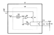
- FIG. 2 is a circuit diagram illustrating a configuration example of the drive unit 100.
- the drive unit 100 of this configuration example is a linear regulator (a so-called LDO [low drop out] regulator) including an output transistor 101, a differential amplifier 102, a digital / analog conversion unit 103, and an operational amplifier 104.
- LDO [low drop out] regulator a so-called LDO [low drop out] regulator
- a voltage Vfb is generated.
- the feedback voltage Vfb increases as the drive current Iout increases, and decreases as the drive current Iout decreases.
- the digital / analog conversion unit 103 converts the digital set value Dset input from the rank adjustment unit 200 into an analog reference voltage Vref.
- the reference voltage Vref increases as the set value Dset increases, and the reference voltage Vref decreases as the set value Dset decreases.
- the reference voltage Vref is variably controlled according to the set value Dset.
- the operational amplifier 104 controls the gate of the output transistor 101 so that the reference voltage Vref input to the non-inverting input terminal (+) matches the feedback voltage Vfb input to the inverting input terminal ( ⁇ ) (imaginary short). I do. With such a configuration, negative feedback control (constant current control) for maintaining the drive current Iout at the target current value corresponding to the set value Dset is realized.
- the drive unit 100 is not limited to a linear regulator, and for example, a switching regulator that generates a desired output voltage Vout from the input voltage Vin by controlling the on-duty of the output transistor may be used.
- FIG. 3 is a circuit diagram illustrating the first embodiment of the rank adjustment unit 200.
- the rank adjustment unit 200 according to the present embodiment includes a current source 211, a switch 212, a voltmeter 213, and a control unit 214.
- the current source 211 is connected between the power supply end and the external terminal T13, and applies the first current I1 to the light emitting string 20.
- the current value of the first current I1 is appropriately set in a range in which the voltage between both ends of each rank resistor R * does not become higher than the forward drop voltage Vf of each light emitting element L *.
- the current value of the first current I1 may be set to less than 33 ⁇ A.
- the switch 212 is connected between the current source 211 and the external terminal T13, and is turned on / off according to an instruction from the control unit 214.
- the switch 212 is turned on only during the rank adjustment period of the light emitting element L *. Therefore, there is no possibility that the rank adjusting unit 200 adversely affects the normal lighting operation of the light emitting string 20.
- the voltmeter 213 is connected between the external terminal T13 and the external terminal T14, and the first voltage V1 that appears across the light emitting string 20 when the first current I1 is applied to the light emitting string 20. , And the measurement result is output to the control unit 214.
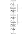
- FIG. 4 is a flowchart showing an example of the rank adjustment operation in the first embodiment. Note that the supply operation of the drive current Iout by the drive unit 100 is stopped while this flow is being executed.
- step S11 the switch 212 is turned on to apply the first current I1 from the current source 211 to the light emitting string 20.
- the rank resistors R1 to R3 have resistance values according to the ranks of the light emitting elements L1 to L3, respectively. Accordingly, the ranks of the light emitting elements L1 to L3 can be detected by calculating the average resistance value Rave of the rank resistances R1 to R3.
- the adjustment process for the set value Dset in step S15 may be performed by referring to a table in which the average resistance value Rave and the set value Dset are associated with each other, for example.
- the drive current Iout is automatically optimized according to the ranks of the light emitting elements L1 to L3, the light emitting element driving device 10 and the light emitting string 20 can be individually designed. That is, since it is not necessary to manually adjust the drive current setting parameters (such as the resistance value of the sense resistor 30) for each lot of the light emitting components 21 to 23, it is possible to reduce work errors. Further, it is not necessary to prepare the same rank products as the light emitting components 21 to 23, and it is sufficient to manage them for each lot, which is advantageous in terms of physical distribution and cost.
- the drive current setting parameters such as the resistance value of the sense resistor 30
- FIG. 5 is a circuit diagram showing a second embodiment of the rank adjustment unit 200.
- the rank adjustment unit 200 of the present embodiment includes a voltage source 221, a switch 222, an ammeter 223, and a control unit 224.
- the voltage source 221 is connected between the external terminal T13 and the external terminal T14, and applies the second voltage V2 to the light emitting string 20.
- the voltage value of the second voltage V2 is appropriately set in a range in which the voltage between both ends of each rank resistor R * does not become higher than the forward voltage drop Vf of each light emitting element L *.
- the voltage value of the second voltage V2 may be set to less than 9.9V.
- the switch 222 is connected between the voltage source 221 and the external terminal T13 (or the external terminal T14), and is turned on / off according to an instruction from the control unit 224.
- the switch 222 is turned on only during the rank adjustment period of the light emitting element L *. Therefore, there is no possibility that the rank adjusting unit 200 adversely affects the normal lighting operation of the light emitting string 20.
- the ammeter 223 is connected between the voltage source 221 and the external terminal T13 (or the external terminal T14), and flows through the light emitting string 20 when the second voltage V2 is applied to the light emitting string 20. Two currents I2 are measured, and the measurement results are output to the control unit 224.
- FIG. 6 is a flowchart showing an example of the rank adjustment operation in the second embodiment. Note that the supply operation of the drive current Iout by the drive unit 100 is stopped while this flow is being executed.
- step S21 the switch 222 is turned on to apply the second voltage V2 from the voltage source 221 to the light emitting string 20.
- the second current I2 is measured using the ammeter 223.
- the rank of the light emitting elements L1 to L3 can be detected from the calculated values, as in the first embodiment.
- the drive current Iout is automatically optimized according to the ranks of the light emitting elements L1 to L3, as in the first embodiment. Therefore, the light emitting element driving device 10 and the light emitting string 20 can be individually designed, and as a result, the same merit as in the first embodiment can be enjoyed.
- FIGS. 7 to 9 are block diagrams showing examples of techniques for causing the rank adjustment unit 200 to recognize the number m of serial stages of light emitting components.
- the light emitting element driving apparatus 10 of the first example further includes external terminals T15a to T15c for receiving information on the number m of series stages.
- information relating to the number m of series stages can be given to the rank adjustment unit 200 by a combination of analog voltages (for example, VCC or GND) applied to the external terminals T15a to T15c.
- the light emitting element driving apparatus 10 of the second example includes a communication interface unit 300 for receiving information on the number m of series stages, an external terminal T16a for receiving an input of a clock signal SCK, and an input of a data signal SDA. And an external terminal T16b. With such a configuration, it is possible to give information on the number m of series stages to the rank adjusting unit 200 without unnecessarily increasing the number of external terminals.
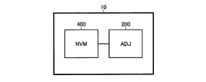
- the light emitting element driving apparatus 10 of the third example further includes a nonvolatile storage unit 400 for storing information regarding the number m of series stages. With such a configuration, information regarding the number m of series stages can be given to the rank adjustment unit 200 without requiring external input.
- a nonvolatile storage unit 400 an EEPROM [electrically erasable programmable read-only memory], an OTPROM [one time programmable ROM], or a flash memory can be suitably used.
- FIG. 10 is a circuit diagram illustrating a third embodiment of the rank adjustment unit 200.
- the rank adjustment unit 200 includes a current source 231, a switch 232, a voltmeter 233, and a control unit 234.
- the current source 231 is connected between the power supply terminal and the external terminal T13, and applies the first current I1 or the third current I3 to the light emitting string 20.
- the current value of the first current I1 is appropriately set within a range in which the voltage across the rank resistors R * does not become higher than the forward voltage drop Vf of each light emitting element L *.
- the current value of the third current I3 is appropriately set within a range in which the voltage between both ends of each rank resistor R * is higher than the forward drop voltage Vf of each light emitting element L *.
- the current source 231 has a first phase in which the third current I3 is applied to the light emitting string 20 and a second phase in which the first current I1 is applied to the light emitting string 20 in accordance with an instruction from the control unit 234. It has a function to switch.
- the switch 232 is connected between the current source 231 and the external terminal T13, and is turned on / off according to an instruction from the control unit 234.
- the switch 232 is turned on only during the rank adjustment period of the light emitting element L *. Therefore, there is no possibility that the rank adjusting unit 200 adversely affects the normal lighting operation of the light emitting string 20.
- the voltmeter 223 is connected between the external terminal T13 and the external terminal T14.
- the third current I3 is applied to the light emitting string 20
- the third voltage V3 that appears across the light emitting string 20 is measured by the voltmeter 223, and the measurement result is output to the control unit 234.
- the first current I ⁇ b> 1 is applied to the light emitting string 20
- the first voltage V ⁇ b> 1 appearing across the light emitting string 20 is measured by the voltmeter 223 and the measurement result is output to the control unit 234.
- FIG. 11 is a flowchart showing an example of the rank adjustment operation in the third embodiment. Note that the supply operation of the drive current Iout by the drive unit 100 is stopped while this flow is being executed. In the following description, it is assumed that the forward drop voltage Vf of each light emitting element L * is a known same value (for example, 3.3 V).
- step S31 the switch 232 is turned on, and the third current I3 is applied from the current source 231 to the light emitting string 20.
- the third voltage V3 is measured using the voltmeter 233.
- the current value of the third current I3 is appropriately set in a range in which the voltage across each rank resistor R * is higher than the forward voltage drop Vf of each light emitting element L *. That is, the third current I1 flows mainly in a current path through the light emitting element L *.
- the above steps S31 to S33 correspond to the first phase described above. That is, the rank adjusting unit 200 of the present embodiment applies a sufficiently large third current I3 (> I1) to the light emitting string 20 in the first phase, and applies the third voltage V3 appearing across the light emitting string 20 at this time.
- I3 third current
- V3 third voltage
- step S11 the first current I1 is applied to the light emitting string 20
- step S12 the first voltage V1 is measured in step S12
- step S15 the set value Dset is adjusted in accordance with the average resistance value Rave.
- the drive current Iout is automatically optimized according to the ranks of the light emitting elements L1 to L3, as in the first embodiment. Therefore, the light emitting element driving device 10 and the light emitting string 20 can be individually designed, and as a result, the same merit as in the first embodiment can be enjoyed.
- FIG. 12 is a circuit diagram illustrating a fourth embodiment of the rank adjustment unit 200.
- the rank adjustment unit 200 of this embodiment includes a current source 241, a voltage source 242, switches 243 to 245, a voltmeter 246, an ammeter 247, and a control unit 248.
- the current source 241 is connected between the power supply terminal and the external terminal T13, and applies the third current I3 to the light emitting string 20 in the first phase.
- the current value of the third current I1 is appropriately set in a range in which the voltage between both ends of each rank resistor R * is higher than the forward voltage drop Vf of each light emitting element L *.
- the voltage source 242 is connected between the external terminal T13 and the external terminal T14, and applies the second voltage V2 to the light emitting string 20 in the second phase.
- the voltage value of the second voltage V2 is appropriately set in a range in which the voltage across the rank resistors R * does not become higher than the forward voltage drop Vf of each light emitting element L *.
- the switch 243 is connected between the current source 241 and the external terminal T13, and is turned on / off according to an instruction from the control unit 248.
- the switch 243 is turned on in the first phase and turned off in the second phase.
- the switch 244 is connected between the voltmeter 246 and the external terminal T13 (or the external terminal T14), and is turned on / off according to an instruction from the control unit 248.
- the switch 244 is turned on in the first phase and turned off in the second phase.
- the switch 245 is connected between the voltage source 242 and the external terminal T13 (or the external terminal T14), and is turned on / off according to an instruction from the control unit 248.
- the switch 245 is turned off in the first phase and turned on in the second phase.
- the switches 243 to 245 are all turned off except during the rank adjustment period of the light emitting element L *. Therefore, there is no possibility that the rank adjusting unit 200 adversely affects the normal lighting operation of the light emitting string 20.
- the voltmeter 246 is connected between the external terminal T13 and the external terminal T14, and a third voltage that appears between both ends of the light emitting string 20 when the third current I3 is applied to the light emitting string 20 in the first phase.
- the voltage V3 is measured and the measurement result is output to the control unit 248.
- the ammeter 247 is connected between the voltage source 242 and the external terminal T13 (or the external terminal T14), and is connected to the light emitting string 20 when the second voltage V2 is applied to the light emitting string 20 in the second phase.
- the flowing second current I2 is measured, and the measurement result is output to the control unit 248.
- FIG. 13 is a flowchart showing an example of the rank adjustment operation in the fourth embodiment. Note that the supply operation of the drive current Iout by the drive unit 100 is stopped while this flow is being executed. In the following description, it is assumed that the forward drop voltage Vf of each light emitting element L * is a known same value (for example, 3.3 V).
- steps S31 to S33 correspond to the first phase described above, and the operation content of each step is basically the same as that of the third embodiment (FIG. 11).
- step S25 the set value Dset is adjusted according to the average resistance value Rave.
- the drive current Iout is automatically optimized according to the ranks of the light emitting elements L1 to L3 as in the second embodiment. Therefore, the light emitting element driving device 10 and the light emitting string 20 can be individually designed, and as a result, the same advantages as those of the second embodiment can be obtained.
- the light-emitting device 1 includes a headlight (including a high beam / low beam / small lamp / fog lamp, etc.) X11, a light source X12 for day / night driving (DRL), a tail lamp (small), as shown in FIGS. (Including lamps and back lamps as appropriate) X13, stop lamp X14, turn lamp X15, and the like.
- a headlight including a high beam / low beam / small lamp / fog lamp, etc.
- DRL day / night driving
- tail lamp small
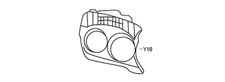
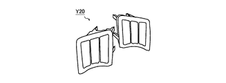
- the light emitting element driving device 10 is provided as a module (LED headlight module Y10 in FIG. 16, LED turn lamp module Y20 in FIG. 17, LED rear lamp module Y30 in FIG. 18, etc.) together with the light emitting string 20 to be driven. It may be provided, or may be provided as a single IC independently of the light-emitting string 20.
- the configuration using a light emitting diode element as a light emitting element has been described as an example.
- the configuration of the present invention is not limited to this, and for example, an organic EL as a light emitting element. It is also possible to use an [electro-luminescence] element.
- the invention disclosed in the present specification can be used for, for example, an in-vehicle exterior lamp, an illumination lamp, and the like (particularly, a light emitting device whose luminance is strictly determined by law or the like).
Landscapes
- Circuit Arrangement For Electric Light Sources In General (AREA)
Abstract
発光素子駆動装置は、発光素子とランク抵抗を並列に内蔵した発光部品に駆動電流を供給する駆動部と;ランク抵抗の抵抗値を読み取って発光素子のランクを検出し、その検出結果に応じて駆動電流の設定値を調整するランク調整部と;を有する。発光素子駆動装置は、同一ロットの発光部品を複数直列に接続して成る発光ストリングを駆動対象とする。なお、発光素子は、例えば、発光ダイオード素子、または、有機EL素子である。また、上記の発光部品と発光素子駆動装置とを有する発光装置が提供される。この発光装置は、例えば、ヘッドライトモジュール、ターンランプモジュール、または、リアランプモジュールとして車両に装着される。
Description
本発明は、発光素子駆動装置に関する。
従来より、発光ダイオード素子や有機EL素子などの発光素子は、その輝度特性(=所定の駆動電流を供給したときに得られる輝度の大きさ)に応じてランク分けされている。
なお、上記に関連する従来技術の一例としては、特許文献1や特許文献2を挙げることができる。
ところで、複数の発光素子を同時駆動する必要のあるアプリケーションにおいて、各発光素子の輝度ばらつきを低減する最も単純な手法は、全ての発光素子を所望の同一ランク品で揃えることである。しかしながら、このような従来手法では、発光装置の設計が容易となる半面、物流面やコスト面で不利であった。
また、別の手法として、全ての発光素子を同一ロット品で揃えることも考えられる。同一ロット品ならば、所望のランク品であるかどうかはさておき、各発光素子毎のランク不揃いが生じるおそれは小さい。従って、ロット毎に駆動電流設定用パラメータ(センス抵抗値など)を適宜調整してやれば、全ての発光素子を所望の輝度で均一に駆動することが可能となる。しかしながら、このような従来手法では、発光素子のロット毎にディスクリート部品の付け替えなどを行う必要があるので、作業ミスの増大を招くおそれがあった。
なお、単一の発光素子を駆動する場合であっても、これを所望の輝度で発光させるためには、発光素子として所望のランク品を用いるか、若しくは、発光素子のランクに応じて駆動電流設定用パラメータを手作業で調整しなければならなかった。
本明細書中に開示されている発明は、本願の発明者らにより見出された上記の問題点に鑑み、発光素子を所望の輝度で発光させることのできる発光素子駆動装置を提供することを目的とする。
本明細書中に開示されている発光素子駆動装置は、発光素子とランク抵抗を並列に内蔵した発光部品に駆動電流を供給する駆動部と;前記ランク抵抗の抵抗値を読み取って前記発光素子のランクを検出し、その検出結果に応じて前記駆動電流の設定値を調整するランク調整部と;を有する構成とされている。
なお、本発明のその他の特徴、要素、ステップ、利点、及び、特性については、以下に続く実施形態の詳細な説明やこれに関する添付の図面によって、さらに明らかとなる。
本明細書中に開示されている発明によれば、発光素子を所望の輝度で発光させることのできる発光素子駆動装置を提供することが可能となる。
<発光装置>
図1は、発光装置1の全体構成例を示すブロック図である。本構成例の発光装置1は、発光素子駆動装置10と、発光ストリング20と、センス抵抗30と、を有する。
図1は、発光装置1の全体構成例を示すブロック図である。本構成例の発光装置1は、発光素子駆動装置10と、発光ストリング20と、センス抵抗30と、を有する。
発光素子駆動装置10は、発光ストリング20を駆動対象とする半導体装置(いわゆるLED[light emitting diode]ドライバIC)であり、駆動部100と、ランク調整部200と、を集積化して成る。
また、発光素子駆動装置10は、装置外部との電気的な接続を確立するための手段として、外部端子T11~T14を備えている。外部端子T11は、入力電圧Vinの入力端子である。外部端子T12は、出力電圧Voutの出力端子である。外部端子T13は、駆動電流Ioutの帰還制御端子である。外部端子T14は、グランドに接続される接地端子である。
駆動部100は、入力電圧Vinから出力電圧Voutを生成して発光ストリング20に供給する。その際、駆動部100は、発光ストリング20に供給される駆動電流Ioutが設定値Dsetに応じた目標電流値となるように負帰還制御(定電流制御)を行う。
ランク調整部200は、発光部品21~23にそれぞれ内蔵されているランク抵抗R1~R3の抵抗値(本実施形態では平均抵抗値Rave(=(R1+R2+R3)/3))を読み取って発光素子L1~L3のランクを検出し、その検出結果に応じて駆動電流Ioutの設定値Dsetを調整する。
発光ストリング20は、発光部品21~23を直列に接続して成る発光部品列である。なお、発光部品の直列段数mは3段に限るものではなく、その用途に応じて任意の直列段数m(ただしm≧1)に設定することが可能である。
発光部品2*(ただし*=1、2、3、以下も同様)は、外部端子T2*a及びT2*bを備え、両外部端子間に発光素子L*とランク抵抗R*を並列に内蔵している。発光素子L*としては、例えば、発光ダイオード素子を好適に用いることができる。ランク抵抗R*は、発光素子L*のランクに応じた抵抗値を持つ。
センス抵抗30(抵抗値:Rs)は、駆動電流Ioutの流れる電流経路上に設けられており、駆動電流Ioutに応じたセンス電圧Vs(=Iout×Rs)を生成する。
なお、以下では、発光部品21~23として同一ロット品が用いられており、ランク抵抗R1~R3の各抵抗値はいずれも同一値(R1=R2=R3=Rave)であることを前提として詳細な説明を行う。
<駆動部>
図2は、駆動部100の一構成例を示す回路図である。本構成例の駆動部100は、出力トランジスタ101と、差動アンプ102と、デジタル/アナログ変換部103と、オペアンプ104と、を含むリニアレギュレータ(いわゆるLDO[low drop out]レギュレータ)である。
図2は、駆動部100の一構成例を示す回路図である。本構成例の駆動部100は、出力トランジスタ101と、差動アンプ102と、デジタル/アナログ変換部103と、オペアンプ104と、を含むリニアレギュレータ(いわゆるLDO[low drop out]レギュレータ)である。
出力トランジスタ101は、外部端子T11(=入力電圧Vinの入力端)と外部端子T12(=出力電圧Voutの出力端)との間に接続されており、オペアンプ104を用いてゲート駆動されるPチャネル型MOS[metal oxide semiconductor]電界効果トランジスタである。
差動アンプ102の非反転入力端(+)は、外部端子T12(=センス抵抗30の高電位端)に接続されている。差動アンプ102の反転入力端(-)は、外部端子T13(=センス抵抗30の低電位端)に接続されている。このように接続された差動アンプ102は、非反転入力端(+)と反転入力端(-)との間に印加されるセンス電圧Vs(=センス抵抗30の両端間電圧)に応じた帰還電圧Vfbを生成する。帰還電圧Vfbは、駆動電流Ioutが大きいほど高くなり、駆動電流Ioutが小さいほど低くなる。
デジタル/アナログ変換部103は、ランク調整部200から入力されるデジタルの設定値Dsetをアナログの基準電圧Vrefに変換する。例えば、設定値Dsetが大きいほど基準電圧Vrefが高くなり、設定値Dsetが小さいほど基準電圧Vrefが低くなる。このように、基準電圧Vrefは、設定値Dsetに応じて可変制御される。
オペアンプ104は、非反転入力端(+)に入力される基準電圧Vrefと、反転入力端(-)に入力される帰還電圧Vfbとが一致(イマジナリショート)するように、出力トランジスタ101のゲート制御を行う。このような構成とすることにより、駆動電流Ioutを設定値Dsetに応じた目標電流値に維持するための負帰還制御(定電流制御)が実現される。
ただし、駆動部100としては、リニアレギュレータに限らず、例えば、出力トランジスタのオンデューティを制御することにより入力電圧Vinから所望の出力電圧Voutを生成するスイッチングレギュレータを用いてもよい。
<ランク調整部(第1実施形態)>
図3は、ランク調整部200の第1実施形態を示す回路図である。本実施形態のランク調整部200は、電流源211と、スイッチ212と、電圧計213と、制御部214とを含む。
図3は、ランク調整部200の第1実施形態を示す回路図である。本実施形態のランク調整部200は、電流源211と、スイッチ212と、電圧計213と、制御部214とを含む。
電流源211は、電源端と外部端子T13との間に接続されており、発光ストリング20に第1電流I1を印加する。第1電流I1の電流値は、各ランク抵抗R*の両端間電圧が各発光素子L*の順方向降下電圧Vfよりも高くならない範囲で適宜設定されている。例えば、ランク抵抗R*の抵抗値が最高100kΩであり、発光素子L*の順方向降下電圧Vfが3.3Vである場合、第1電流I1の電流値は33μA未満に設定するとよい。
スイッチ212は、電流源211と外部端子T13との間に接続されており、制御部214からの指示に応じてオン/オフされる。なお、スイッチ212は、発光素子L*のランク調整期間にのみオンされる。従って、ランク調整部200が発光ストリング20の通常点灯動作に悪影響を及ぼすおそれはない。
電圧計213は、外部端子T13と外部端子T14との間に接続されており、発光ストリング20に対して第1電流I1が印加されているときに発光ストリング20の両端間に現れる第1電圧V1を測定し、その測定結果を制御部214に出力する。
制御部214は、第1電流I1と第1電圧V1から算出されるランク抵抗R1~R3の合成抵抗値Rtotal(=V1/I1=R1+R2+R3)を発光部品21~23の直列段数m(=3)で除算し、その演算結果(=発光素子L1~L3のランク検出結果)に応じて駆動電流Ioutの設定値Dsetを調整する。
以下では、制御部214によるランク調整動作について、フローチャートを参照しながら詳細に説明する。
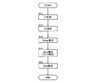
図4は、第1実施形態におけるランク調整動作の一例を示すフローチャートである。なお、本フローが実行されている間、駆動部100による駆動電流Ioutの供給動作は停止されているものとする。
本フローが開始されると、まず、ステップS11では、スイッチ212をオンすることにより、電流源211から発光ストリング20に対して第1電流I1の印加が行われる。
続くステップS12では、電圧計213を用いて、第1電圧V1の測定が行われる。先にも述べたように、第1電流I1を印加しても各ランク抵抗R*の両端間電圧が各発光素子L*の順方向降下電圧Vfを上回ることはない。すなわち、第1電流I1は、発光素子L*を介する電流経路には流れず、ランク抵抗R*を介する電流経路にのみ流れる。従って、第1電圧V1は、ランク抵抗R1~R3の合成抵抗値Rtotal(=R1+R2+R3)に第1電流I1を乗じた電圧値(=Rtotal×I1)となる。
続くステップS13では、制御部214により、第1電流I1と第1電圧V1からランク抵抗R1~R3の合成抵抗値Rtotal(=V1/I1)が算出される。
続くステップS14では、制御部214により、ランク抵抗R1~R3の合成抵抗値Rtotalと、発光部品21~23の直列段数m(=3)から、ランク抵抗R1~R3の平均抵抗値Rave(=Rtotal/m)が算出される。なお、先にも述べたように、発光部品21~23としては、いずれも同一ロット品が用いられており、ランク抵抗R1~R3の各抵抗値は、いずれも同一値(R1=R2=R3)である。従って、ステップS14で算出される平均抵抗値Raveは、ランク抵抗R1~R3の各抵抗値と一致する。
また、先にも述べたように、ランク抵抗R1~R3は、それぞれ、発光素子L1~L3のランクに応じた抵抗値を持っている。従って、ランク抵抗R1~R3の平均抵抗値Raveを算出することにより、発光素子L1~L3のランクを検出することができる。
続くステップS15では、制御部214により、ランク抵抗R1~R3の平均抵抗値Rave(=発光素子L1~L3のランク検出結果)に応じた設定値Dsetの調整が行われた後、一連のフローが終了される。なお、ステップS15における設定値Dsetの調整処理については、例えば、平均抵抗値Raveと設定値Dsetとを対応付けたテーブルを参照することにより実施すればよい。
このような構成であれば、発光素子L1~L3のランクに応じて駆動電流Ioutが自動的に最適化されるので、発光素子駆動装置10と発光ストリング20とを個別に設計することができる。すなわち、発光部品21~23のロット毎に駆動電流設定用パラメータ(センス抵抗30の抵抗値など)を手作業で調整する必要がないので、作業ミスを減らすことが可能となる。また、発光部品21~23として、所望の同一ランク品を揃える必要はなく、ロット毎に管理すれば足りるので、物流面やコスト面でも有利となる。
<ランク調整部(第2実施形態)>
図5は、ランク調整部200の第2実施形態を示す回路図である。本実施形態のランク調整部200は、電圧源221と、スイッチ222と、電流計223と、制御部224とを含む。
図5は、ランク調整部200の第2実施形態を示す回路図である。本実施形態のランク調整部200は、電圧源221と、スイッチ222と、電流計223と、制御部224とを含む。
電圧源221は、外部端子T13と外部端子T14との間に接続されており、発光ストリング20に第2電圧V2を印加する。第2電圧V2の電圧値は、各ランク抵抗R*の両端間電圧が各発光素子L*の順方向降下電圧Vfよりも高くならない範囲で適宜設定されている。例えば、発光素子L*の順方向降下電圧Vfが3.3Vであり、直列段数mが3である場合、第2電圧V2の電圧値は9.9V未満に設定するとよい。
スイッチ222は、電圧源221と外部端子T13(または外部端子T14)との間に接続されており、制御部224からの指示に応じてオン/オフされる。なお、スイッチ222は、発光素子L*のランク調整期間にのみオンされる。従って、ランク調整部200が発光ストリング20の通常点灯動作に悪影響を及ぼすおそれはない。
電流計223は、電圧源221と外部端子T13(または外部端子T14)との間に接続されており、発光ストリング20に対して第2電圧V2が印加されているときに発光ストリング20に流れる第2電流I2を測定し、その測定結果を制御部224に出力する。
制御部224は、第2電流I2と第2電圧V2から算出されるランク抵抗R1~R3の合成抵抗値Rtotal(=V2/I2=R1+R2+R3)を発光部品21~23の直列段数m(=3)で除算し、その演算結果(=発光素子L1~L3のランク検出結果)に応じて駆動電流Ioutの設定値Dsetを調整する。
以下では、制御部224によるランク調整動作について、フローチャートを参照しながら詳細に説明する。
図6は、第2実施形態におけるランク調整動作の一例を示すフローチャートである。なお、本フローが実行されている間、駆動部100による駆動電流Ioutの供給動作は停止されているものとする。
本フローが開始されると、まず、ステップS21では、スイッチ222をオンすることにより、電圧源221から発光ストリング20に対して第2電圧V2の印加が行われる。
続くステップS22では、電流計223を用いて、第2電流I2の測定が行われる。先にも述べたように、第2電圧V2を印加しても、各ランク抵抗R*の両端間電圧が各発光素子L*の順方向降下電圧Vfを上回ることはない。すなわち、第2電流I2は、発光素子L*を介する電流経路には流れず、ランク抵抗R*を介する電流経路にのみ流れる。従って、第2電流I2は、第2電圧V2をランク抵抗R1~R3の合成抵抗値Rtotal(=R1+R2+R3)で除した電流値(=V2/Rtotal)となる。
続くステップS23では、制御部224により、第2電流I2と第2電圧V2からランク抵抗R1~R3の合成抵抗値Rtotal(=V2/I2)が算出される。
続くステップS24では、制御部224により、ランク抵抗R1~R3の合成抵抗値Rtotalと、発光部品21~23の直列段数m(=3)から、ランク抵抗R1~R3の平均抵抗値Rave(=Rtotal/m)が算出される。この算出値から発光素子L1~L3のランクを検出することができる点については、先の第1実施形態と同様である。
続くステップS25では、制御部224により、ランク抵抗R1~R3の平均抵抗値Rave(=発光素子L1~L3のランク検出結果)に応じた設定値Dsetの調整が行われた後、一連のフローが終了される。なお、ステップS25における設定値Dsetの調整処理については、例えば、平均抵抗値Raveと設定値Dsetとを対応付けたテーブルを参照することにより実施すればよい。
このような構成であれば、先の第1実施形態と同じく、発光素子L1~L3のランクに応じて駆動電流Ioutが自動的に最適化される。従って、発光素子駆動装置10と発光ストリング20とを個別に設計することが可能となり、延いては、先の第1実施形態と同様のメリットを享受することが可能となる。
<段数認識手法>
図7~図9は、それぞれ、ランク調整部200に発光部品の直列段数mを認識させる手法の一例を示すブロック図である。
図7~図9は、それぞれ、ランク調整部200に発光部品の直列段数mを認識させる手法の一例を示すブロック図である。
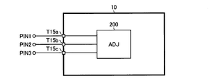
第1例(図7)の発光素子駆動装置10は、直列段数mに関する情報を受け付けるための外部端子T15a~T15cをさらに有する。このような構成であれば、外部端子T15a~T15cにそれぞれ印加されるアナログ電圧(例えばVCCまたはGND)の組み合わせにより、直列段数mに関する情報をランク調整部200に与えることができる。
第2例(図8)の発光素子駆動装置10は、直列段数mに関する情報を受け付けるための通信インタフェイス部300と、クロック信号SCKの入力を受け付けるための外部端子T16aと、データ信号SDAの入力を受け付けるための外部端子T16bと、をさらに有する。このような構成とすることにより、外部端子の本数を不必要に増大することなく、直列段数mに関する情報をランク調整部200に与えることが可能となる。
第3例(図9)の発光素子駆動装置10は、直列段数mに関する情報を格納するための不揮発性記憶部400をさらに有する。このような構成であれば、外部入力を要することなく、直列段数mに関する情報をランク調整部200に与えることができる。なお、不揮発性記憶部400としては、EEPROM[electrically erasable programmable read-only memory]やOTPROM[one time programmable ROM]、ないしは、フラッシュメモリなどを好適に用いることができる。
<ランク調整部(第3実施形態)>
図10は、ランク調整部200の第3実施形態を示す回路図である。本実施形態のランク調整部200は、電流源231と、スイッチ232と、電圧計233と、制御部234とを含む。
図10は、ランク調整部200の第3実施形態を示す回路図である。本実施形態のランク調整部200は、電流源231と、スイッチ232と、電圧計233と、制御部234とを含む。
電流源231は、電源端と外部端子T13との間に接続されており、発光ストリング20に第1電流I1または第3電流I3を印加する。第1電流I1の電流値は、先にも述べたように、各ランク抵抗R*の両端間電圧が各発光素子L*の順方向降下電圧Vfよりも高くならない範囲で適宜設定されている。一方、第3電流I3の電流値は、各ランク抵抗R*の両端間電圧が各発光素子L*の順方向降下電圧Vfよりも高くなる範囲で適宜設定されている。なお、電流源231は、制御部234からの指示に応じて、発光ストリング20に第3電流I3を印加する第1フェイズと、発光ストリング20に第1電流I1を印加する第2フェイズと、を切り替える機能を備えている。
スイッチ232は、電流源231と外部端子T13との間に接続されており、制御部234からの指示に応じてオン/オフされる。なお、スイッチ232は、発光素子L*のランク調整期間にのみオンされる。従って、ランク調整部200が発光ストリング20の通常点灯動作に悪影響を及ぼすおそれはない。
電圧計223は、外部端子T13と外部端子T14との間に接続されている。発光ストリング20に第3電流I3が印加される第1フェイズでは、発光ストリング20の両端間に現れる第3電圧V3が電圧計223で測定され、その測定結果が制御部234に出力される。一方、発光ストリング20に第1電流I1が印加される第2フェイズでは、発光ストリング20の両端間に現れる第1電圧V1が電圧計223で測定され、その測定結果が制御部234に出力される。
制御部234は、第1フェイズにおいて、第3電圧V3から発光部品21~23の直列段数m(=3)を求める。その後、制御部234は、第2フェイズにおいて、第1電流I1と第1電圧V1から算出されるランク抵抗R1~R3の合成抵抗値Rtotal(=V1/I1=R1+R2+R3)を発光部品21~23の直列段数mで除算し、その演算結果(=発光素子L1~L3のランク検出結果)に応じて、駆動電流Ioutの設定値Dsetを調整する。
以下では、制御部234によるランク調整動作について、フローチャートを参照しながら詳細に説明する。
図11は、第3実施形態におけるランク調整動作の一例を示すフローチャートである。なお、本フローが実行されている間、駆動部100による駆動電流Ioutの供給動作は停止されているものとする。また、以下では、各発光素子L*の順方向降下電圧Vfがいずれも既知の同一値(例えば3.3V)であるものとして説明する。
本フローが開始されると、まず、ステップS31では、スイッチ232をオンするとともに、電流源231から発光ストリング20に対して第3電流I3の印加が行われる。
続くステップS32では、電圧計233を用いて、第3電圧V3の測定が行われる。先にも述べた通り、第3電流I3の電流値は、各ランク抵抗R*の両端間電圧が各発光素子L*の順方向降下電圧Vfよりも高くなる範囲で適宜設定されている。すなわち、第3電流I1は、主として発光素子L*を介する電流経路に流れる。従って、第3電圧V3は、各発光素子L*の順方向降下電圧Vfに発光部品21~23の直列段数mを乗じた電圧値(=Vf×m)となる。
続くステップS33では、制御部234により、第3電圧V3を各発光素子L*の順方向降下電圧Vfで除すことにより、発光部品21~23の直列段数m(=V3/Vf)が算出される。
上記のステップS31~S33は、先述の第1フェイズに相当する。すなわち、本実施形態のランク調整部200は、第1フェイズにおいて、発光ストリング20に十分大きな第3電流I3(>I1)を印加し、このとき発光ストリング20の両端間に現れる第3電圧V3を測定することにより、発光部品21~23の直列段数mを自ら求めることができる。従って、直列段数mに関する情報をランク調整部200に与えるための構成要素(図7~図9を参照)が不要となるので、外部端子数の削減や回路規模の縮小が可能となる。
なお、続くステップS11~S15は、先述の第2フェイズに相当するものであり、各ステップの動作内容は、第1実施形態(図4)のそれと基本的に同一である。ごく簡単に説明すると、ステップS11では、発光ストリング20に第1電流I1が印加され、ステップS12では、第1電圧V1が測定され、ステップS13では、合成抵抗値Rtotal(=I1/V1)が算出され、ステップS14では、平均抵抗値Rave(=Rtotal/m)が算出され、ステップS15では、平均抵抗値Raveに応じて設定値Dsetが調整される。
このような構成であれば、先の第1実施形態と同じく、発光素子L1~L3のランクに応じて駆動電流Ioutが自動的に最適化される。従って、発光素子駆動装置10と発光ストリング20とを個別に設計することが可能となり、延いては、先の第1実施形態と同様のメリットを享受することが可能となる。
<ランク調整部(第4実施形態)>
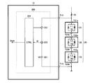
図12は、ランク調整部200の第4実施形態を示す回路図である。本実施形態のランク調整部200は、電流源241と、電圧源242と、スイッチ243~245と、電圧計246と、電流計247と、制御部248と、を含む。
図12は、ランク調整部200の第4実施形態を示す回路図である。本実施形態のランク調整部200は、電流源241と、電圧源242と、スイッチ243~245と、電圧計246と、電流計247と、制御部248と、を含む。
電流源241は、電源端と外部端子T13との間に接続されており、第1フェイズにおいて発光ストリング20に第3電流I3を印加する。第3電流I1の電流値は、先にも述べたように、各ランク抵抗R*の両端間電圧が各発光素子L*の順方向降下電圧Vfよりも高くなる範囲で適宜設定されている。
電圧源242は、外部端子T13と外部端子T14との間に接続されており、第2フェイズにおいて発光ストリング20に第2電圧V2を印加する。第2電圧V2の電圧値は、先にも述べたように、各ランク抵抗R*の両端間電圧が各発光素子L*の順方向降下電圧Vfよりも高くならない範囲で適宜設定されている。
スイッチ243は、電流源241と外部端子T13との間に接続されており、制御部248からの指示に応じてオン/オフされる。なお、スイッチ243は、第1フェイズでオンされ、第2フェイズでオフされる。
スイッチ244は、電圧計246と外部端子T13(または外部端子T14)との間に接続されており、制御部248からの指示に応じてオン/オフされる。なお、スイッチ244は、第1フェイズでオンされ、第2フェイズでオフされる。
スイッチ245は、電圧源242と外部端子T13(または外部端子T14)との間に接続されており、制御部248からの指示に応じてオン/オフされる。なお、スイッチ245は、第1フェイズでオフされ、第2フェイズでオンされる。
また、発光素子L*のランク調整期間以外では、スイッチ243~245がいずれもオフされる。従って、ランク調整部200が発光ストリング20の通常点灯動作に悪影響を及ぼすおそれはない。
電圧計246は、外部端子T13と外部端子T14との間に接続されており、第1フェイズにおいて発光ストリング20に第3電流I3が印加されているときに発光ストリング20の両端間に現れる第3電圧V3を測定し、その測定結果を制御部248に出力する。
電流計247は、電圧源242と外部端子T13(または外部端子T14)との間に接続されており、第2フェイズにおいて発光ストリング20に第2電圧V2が印加されているときに発光ストリング20に流れる第2電流I2を測定し、その測定結果を制御部248に出力する。
制御部248は、第1フェイズにおいて、第3電圧V3から発光部品21~23の直列段数m(=3)を求める。その後、制御部234は、第2フェイズにおいて、第2電流I2と第2電圧V2から算出されるランク抵抗R1~R3の合成抵抗値Rtotal(=V2/I2=R1+R2+R3)を発光部品21~23の直列段数mで除算し、その演算結果(=発光素子L1~L3のランク検出結果)に応じて、駆動電流Ioutの設定値Dsetを調整する。
以下では、制御部248によるランク調整動作について、フローチャートを参照しながら詳細に説明する。
図13は、第4実施形態におけるランク調整動作の一例を示すフローチャートである。なお、本フローが実行されている間、駆動部100による駆動電流Ioutの供給動作は停止されているものとする。また、以下では、各発光素子L*の順方向降下電圧Vfがいずれも既知の同一値(例えば3.3V)であるものとして説明する。
本フローにおいて、ステップS31~S33は、先述の第1フェイズに相当するものであり、各ステップの動作内容は、第3実施形態(図11)のそれと基本的に同一である。ごく簡単に説明すると、ステップS31では、発光ストリング20に第3電流I3が印加され、ステップS32では、第3電圧V3が測定され、ステップS33では、直列段数m(=V3/Vf)が算出される。
このように、直列段数mを自ら求める構成であれば、先の第3実施形態と同様、直列段数mに関する情報をランク調整部200に与えるための構成要素(図7~図9を参照)が不要となるので、外部端子数の削減や回路規模の縮小が可能となる。
また、続くステップS21~S25は、先述の第2フェイズに相当するものであり、各ステップの動作内容は、第2実施形態(図6)のそれと基本的に同一である。ごく簡単に説明すると、ステップS21では、発光ストリング20に第2電圧V2が印加され、ステップS22では、第2電流I2が測定され、ステップS23では、合成抵抗値Rtotal(=I2/V2)が算出され、ステップS24では、平均抵抗値Rave(=Rtotal/m)が算出され、ステップS25では、平均抵抗値Raveに応じて設定値Dsetが調整される。
このような構成であれば、先の第2実施形態と同じく、発光素子L1~L3のランクに応じて駆動電流Ioutが自動的に最適化される。従って、発光素子駆動装置10と発光ストリング20とを個別に設計することが可能となり、延いては、先の第2実施形態と同様のメリットを享受することが可能となる。
<車両への適用>
発光装置1は、例えば、図14及び図15で示す通り、車両X10のヘッドライト(ハイビーム/ロービーム/スモールランプ/フォグランプなどを適宜含む)X11、白昼夜走行(DRL)用光源X12、テールランプ(スモールランプやバックランプなどを適宜含む)X13、ストップランプX14、及び、ターンランプX15などとして好適に用いることができる。
発光装置1は、例えば、図14及び図15で示す通り、車両X10のヘッドライト(ハイビーム/ロービーム/スモールランプ/フォグランプなどを適宜含む)X11、白昼夜走行(DRL)用光源X12、テールランプ(スモールランプやバックランプなどを適宜含む)X13、ストップランプX14、及び、ターンランプX15などとして好適に用いることができる。
なお、発光素子駆動装置10は、駆動対象となる発光ストリング20と共にモジュール(図16のLEDヘッドライトモジュールY10、図17のLEDターンランプモジュールY20、及び、図18のLEDリアランプモジュールY30など)として提供されるものであってもよいし、発光ストリング20とは独立にIC単体として提供されるものであってもよい。
<その他の変形例>
なお、上記の実施形態では、発光素子として発光ダイオード素子を用いた構成を例に挙げて説明を行ったが、本発明の構成はこれに限定されるものではなく、例えば、発光素子として有機EL[electro-luminescence]素子を用いることも可能である。
なお、上記の実施形態では、発光素子として発光ダイオード素子を用いた構成を例に挙げて説明を行ったが、本発明の構成はこれに限定されるものではなく、例えば、発光素子として有機EL[electro-luminescence]素子を用いることも可能である。
このように、本明細書中に開示されている種々の技術的特徴は、上記実施形態のほか、その技術的創作の主旨を逸脱しない範囲で種々の変更を加えることが可能である。すなわち、上記実施形態は、全ての点で例示であって、制限的なものではないと考えられるべきであり、本発明の技術的範囲は、上記実施形態の説明ではなく、特許請求の範囲によって示されるものであり、特許請求の範囲と均等の意味及び範囲内に属する全ての変更が含まれると理解されるべきである。
本明細書中に開示されている発明は、例えば、車載用エクステリアランプやイルミネーションランプなど(特に、法律などにより輝度が厳格に定められている発光装置)に利用することが可能である。
1 発光装置
10 発光素子駆動装置
20 発光ストリング
21、22、23 発光部品
30 センス抵抗
40 スイッチ駆動装置
50 マイコン
100 駆動部
101 出力トランジスタ(Pチャネル型MOS電界効果トランジスタ)
102 差動アンプ
103 デジタル/アナログ変換部
104 オペアンプ
200 ランク調整部
211、231、241 電流源
221、242 電圧源
212、222、232、243~245 スイッチ
213、233、246 電圧計
223、247 電流計
214、224、234、248 制御部
300 通信インタフェイス部
400 不揮発性記憶部
L1、L2、L3 発光素子(発光ダイオード)
R1、R2、R3 ランク抵抗
P1~P6 Pチャネル型MOS電界効果トランジスタ
T11~T14、T21~T23 外部端子
X10 車両
X11 ヘッドライト
X12 白昼夜走行(DRL)用光源
X13 テールランプ
X14 ストップランプ
X15 ターンランプ
Y10 LEDヘッドライトモジュール
Y20 LEDターンランプモジュール
Y30 LEDリアランプモジュール
10 発光素子駆動装置
20 発光ストリング
21、22、23 発光部品
30 センス抵抗
40 スイッチ駆動装置
50 マイコン
100 駆動部
101 出力トランジスタ(Pチャネル型MOS電界効果トランジスタ)
102 差動アンプ
103 デジタル/アナログ変換部
104 オペアンプ
200 ランク調整部
211、231、241 電流源
221、242 電圧源
212、222、232、243~245 スイッチ
213、233、246 電圧計
223、247 電流計
214、224、234、248 制御部
300 通信インタフェイス部
400 不揮発性記憶部
L1、L2、L3 発光素子(発光ダイオード)
R1、R2、R3 ランク抵抗
P1~P6 Pチャネル型MOS電界効果トランジスタ
T11~T14、T21~T23 外部端子
X10 車両
X11 ヘッドライト
X12 白昼夜走行(DRL)用光源
X13 テールランプ
X14 ストップランプ
X15 ターンランプ
Y10 LEDヘッドライトモジュール
Y20 LEDターンランプモジュール
Y30 LEDリアランプモジュール
Claims (14)
- 発光素子とランク抵抗を並列に内蔵した発光部品に駆動電流を供給する駆動部と;
前記ランク抵抗の抵抗値を読み取って前記発光素子のランクを検出し、その検出結果に応じて前記駆動電流の設定値を調整するランク調整部と;
を有することを特徴とする発光素子駆動装置。 - 同一ロットの前記発光部品を複数直列に接続して成る発光ストリングを駆動対象とすることを特徴とする請求項1に記載の発光素子駆動装置。
- 前記ランク調整部は、
各ランク抵抗の両端間電圧が各発光素子の順方向降下電圧よりも高くならない範囲で前記発光ストリングに所定の第1電流を印加する電流源と;
前記第1電流が印加されているときに前記発光ストリングの両端間に現れる第1電圧を測定する電圧計と;
前記第1電流と前記第1電圧から算出される全ランク抵抗の合成抵抗値を前記発光部品の直列段数で除算し、その演算結果に応じて前記駆動電流の設定値を調整する制御部と;
を含むことを特徴とする請求項2に記載の発光素子駆動装置。 - 前記ランク調整部は、
各ランク抵抗の両端間電圧が各発光素子の順方向降下電圧よりも高くならない範囲で前記発光ストリングに所定の第2電圧を印加する電圧源と;
前記第2電圧が印加されているときに前記発光ストリングに流れる第2電流を測定する電流計と;
前記第2電流と前記第2電圧から算出される全ランク抵抗の合成抵抗値を前記発光部品の直列段数で除算し、その演算結果に応じて前記駆動電流の設定値を調整する制御部と;
を含むことを特徴とする請求項2に記載の発光素子駆動装置。 - 前記直列段数に関する情報を受け付けるための外部端子をさらに有することを特徴とする請求項3または請求項4に記載の発光素子駆動装置。
- 前記直列段数に関する情報を受け付けるための通信インタフェイス部をさらに有することを特徴とする請求項3または請求項4に記載の発光素子駆動装置。
- 前記直列段数に関する情報を格納するための不揮発性記憶部をさらに有することを特徴とする請求項3または請求項4に記載の発光素子駆動装置。
- 前記ランク調整部は、
各ランク抵抗の両端間電圧が各発光素子の順方向降下電圧よりも高くなる範囲で前記発光ストリングに所定の第3電流を印加する第1フェイズと、各ランク抵抗の両端間電圧が各発光素子の順方向降下電圧よりも高くならない範囲で前記発光ストリングに所定の第1電流を印加する第2フェイズとを切り替えることのできる電流源と;
前記第1フェイズにおいて前記第3電流が印加されているときに前記発光ストリングの両端間に現れる第3電圧、及び、前記第2フェイズにおいて前記第1電流が印加されているときに前記発光ストリングの両端間に現れる第1電圧をそれぞれ測定する電圧計と;
前記第1フェイズにおいて前記第3電圧から前記発光部品の直列段数を求めた上で、前記第2フェイズにおいて前記第1電流と前記第1電圧から算出される全ランク抵抗の合成抵抗値を前記直列段数で除算し、その演算結果に応じて前記駆動電流の設定値を調整する制御部と;
を含むことを特徴とする請求項2に記載の発光素子駆動装置。 - 前記ランク調整部は、
第1フェイズにおいて各ランク抵抗の両端間電圧が各発光素子の順方向降下電圧よりも高くなる範囲で前記発光ストリングに所定の第3電流を印加する電流源と;
前記第1フェイズにおいて前記第3電流が印加されているときに前記発光ストリングの両端間に現れる第3電圧を測定する電圧計と;
第2フェイズにおいて各ランク抵抗の両端間電圧が各発光素子の順方向降下電圧よりも高くならない範囲で前記発光ストリングに所定の第2電圧を印加する電圧源と;
前記第2フェイズにおいて前記第2電圧が印加されているときに前記発光ストリングに流れる第2電流を測定する電流計と;
前記第1フェイズにおいて前記第3電圧から前記発光部品の直列段数を求めた上で、前記第2フェイズにおいて前記第2電流と前記第2電圧から算出される全ランク抵抗の合成抵抗値を前記直列段数で除算し、その演算結果に応じて前記駆動電流の設定値を調整する制御部と;
を含むことを特徴とする請求項2に記載の発光素子駆動装置。 - 発光素子とランク抵抗を並列に内蔵した発光部品と、
請求項1~請求項9のいずれか一項に記載の発光素子駆動装置と、
を有することを特徴とする発光装置。 - 前記発光素子は、発光ダイオード素子、または、有機EL素子であることを特徴とする請求項10に記載の発光装置。
- ヘッドライトモジュール、ターンランプモジュール、または、リアランプモジュールとして車両に装着されることを特徴とする請求項10または請求項11に記載の発光装置。
- 請求項10~請求項12のいずれか一項に記載の発光装置を有する車両。
- 前記発光装置は、ヘッドライト、白昼夜走行用光源、テールランプ、ストップランプ、及び、ターンランプの少なくとも一つとして用いられることを特徴とする請求項13に記載の車両。
Applications Claiming Priority (2)
| Application Number | Priority Date | Filing Date | Title |
|---|---|---|---|
| JP2015107373A JP2016225026A (ja) | 2015-05-27 | 2015-05-27 | 発光素子駆動装置 |
| JP2015-107373 | 2015-05-27 |
Publications (1)
| Publication Number | Publication Date |
|---|---|
| WO2016189979A1 true WO2016189979A1 (ja) | 2016-12-01 |
Family
ID=57392717
Family Applications (1)
| Application Number | Title | Priority Date | Filing Date |
|---|---|---|---|
| PCT/JP2016/061335 Ceased WO2016189979A1 (ja) | 2015-05-27 | 2016-04-07 | 発光素子駆動装置 |
Country Status (2)
| Country | Link |
|---|---|
| JP (1) | JP2016225026A (ja) |
| WO (1) | WO2016189979A1 (ja) |
Cited By (1)
| Publication number | Priority date | Publication date | Assignee | Title |
|---|---|---|---|---|
| TWI651221B (zh) * | 2017-05-17 | 2019-02-21 | 誠益光電科技股份有限公司 | 車燈裝置及其遮板驅動模組 |
Families Citing this family (1)
| Publication number | Priority date | Publication date | Assignee | Title |
|---|---|---|---|---|
| JP7341603B2 (ja) * | 2019-05-29 | 2023-09-11 | Idec株式会社 | 発光装置及び発光装置の製造方法 |
Citations (5)
| Publication number | Priority date | Publication date | Assignee | Title |
|---|---|---|---|---|
| JP2004158840A (ja) * | 2002-10-16 | 2004-06-03 | Ccs Inc | Led照明装置用電源システム |
| JP2012216862A (ja) * | 2007-12-05 | 2012-11-08 | Toshiba Lighting & Technology Corp | 発光ユニット及び発光装置 |
| JP2013026024A (ja) * | 2011-07-21 | 2013-02-04 | Mitsubishi Electric Corp | 光源点灯システム及び照明システム |
| JP2013522819A (ja) * | 2010-03-10 | 2013-06-13 | コーニンクレッカ フィリップス エレクトロニクス エヌ ヴィ | 異なるled種類を有するled照明装置における色の一致の維持 |
| JP2014159248A (ja) * | 2013-02-20 | 2014-09-04 | Stanley Electric Co Ltd | 車両用灯具 |
-
2015
- 2015-05-27 JP JP2015107373A patent/JP2016225026A/ja active Pending
-
2016
- 2016-04-07 WO PCT/JP2016/061335 patent/WO2016189979A1/ja not_active Ceased
Patent Citations (5)
| Publication number | Priority date | Publication date | Assignee | Title |
|---|---|---|---|---|
| JP2004158840A (ja) * | 2002-10-16 | 2004-06-03 | Ccs Inc | Led照明装置用電源システム |
| JP2012216862A (ja) * | 2007-12-05 | 2012-11-08 | Toshiba Lighting & Technology Corp | 発光ユニット及び発光装置 |
| JP2013522819A (ja) * | 2010-03-10 | 2013-06-13 | コーニンクレッカ フィリップス エレクトロニクス エヌ ヴィ | 異なるled種類を有するled照明装置における色の一致の維持 |
| JP2013026024A (ja) * | 2011-07-21 | 2013-02-04 | Mitsubishi Electric Corp | 光源点灯システム及び照明システム |
| JP2014159248A (ja) * | 2013-02-20 | 2014-09-04 | Stanley Electric Co Ltd | 車両用灯具 |
Cited By (1)
| Publication number | Priority date | Publication date | Assignee | Title |
|---|---|---|---|---|
| TWI651221B (zh) * | 2017-05-17 | 2019-02-21 | 誠益光電科技股份有限公司 | 車燈裝置及其遮板驅動模組 |
Also Published As
| Publication number | Publication date |
|---|---|
| JP2016225026A (ja) | 2016-12-28 |
Similar Documents
| Publication | Publication Date | Title |
|---|---|---|
| JP6510921B2 (ja) | チャージポンプ、スイッチ駆動装置、発光装置、車両 | |
| JP6641080B2 (ja) | 発光素子駆動装置、発光装置、車両 | |
| JP5591848B2 (ja) | 適応スイッチモードledシステム | |
| US8981667B2 (en) | Current controlling circuit for a light-emitting diode driver and producing method therefor | |
| JP6899695B2 (ja) | 発光素子駆動装置及びその駆動方法 | |
| JP6502054B2 (ja) | 発光素子駆動装置、発光素子駆動回路、発光装置、車両 | |
| US9807837B2 (en) | Light-emitting apparatus, luminaire, and method of adjusting light-emitting apparatus | |
| TWI790306B (zh) | Led陣列之驅動器 | |
| US9980331B2 (en) | Oscillation circuit | |
| JP5230004B2 (ja) | 車両用灯具の点灯制御装置 | |
| TW202324890A (zh) | 恆流驅動裝置及其電流調整方法和led驅動裝置 | |
| WO2016189979A1 (ja) | 発光素子駆動装置 | |
| JP7345360B2 (ja) | 半導体発光素子の点灯制御方法並びに点灯制御装置、発光装置 | |
| WO2016194469A1 (ja) | 発光素子駆動装置、スイッチ駆動装置 | |
| JP2005110356A (ja) | 負荷駆動装置及び携帯機器 | |
| JP7736488B2 (ja) | 発光素子駆動用半導体集積回路、発光素子駆動装置、発光装置、車両 | |
| JP2007299827A (ja) | 半導体集積回路 | |
| CN112369124B (zh) | 光源驱动装置及其方法 | |
| JP6859022B2 (ja) | Led照明用調光装置 | |
| CN112992051B (zh) | Led显示器的恒流源校正装置及其方法 | |
| US10491115B2 (en) | Arrangement and method for delivering a current-controlled voltage | |
| KR20160114464A (ko) | 차량 램프의 전류 제어 장치 | |
| JP2016076315A (ja) | 発光素子駆動装置、発光装置、車両 | |
| KR20170054126A (ko) | Led 램프용 디밍 장치 |
Legal Events
| Date | Code | Title | Description |
|---|---|---|---|
| 121 | Ep: the epo has been informed by wipo that ep was designated in this application |
Ref document number: 16799687 Country of ref document: EP Kind code of ref document: A1 |
|
| NENP | Non-entry into the national phase |
Ref country code: DE |
|
| 122 | Ep: pct application non-entry in european phase |
Ref document number: 16799687 Country of ref document: EP Kind code of ref document: A1 |