WO2016178266A1 - 撮像装置 - Google Patents
撮像装置 Download PDFInfo
- Publication number
- WO2016178266A1 WO2016178266A1 PCT/JP2015/063073 JP2015063073W WO2016178266A1 WO 2016178266 A1 WO2016178266 A1 WO 2016178266A1 JP 2015063073 W JP2015063073 W JP 2015063073W WO 2016178266 A1 WO2016178266 A1 WO 2016178266A1
- Authority
- WO
- WIPO (PCT)
- Prior art keywords
- pixel
- signal
- pixels
- substrate
- light
- Prior art date
- Legal status (The legal status is an assumption and is not a legal conclusion. Google has not performed a legal analysis and makes no representation as to the accuracy of the status listed.)
- Ceased
Links
Images







Classifications
-
- H—ELECTRICITY
- H04—ELECTRIC COMMUNICATION TECHNIQUE
- H04N—PICTORIAL COMMUNICATION, e.g. TELEVISION
- H04N25/00—Circuitry of solid-state image sensors [SSIS]; Control thereof
- H04N25/10—Circuitry of solid-state image sensors [SSIS]; Control thereof for transforming different wavelengths into image signals
- H04N25/11—Arrangement of colour filter arrays [CFA]; Filter mosaics
- H04N25/13—Arrangement of colour filter arrays [CFA]; Filter mosaics characterised by the spectral characteristics of the filter elements
- H04N25/134—Arrangement of colour filter arrays [CFA]; Filter mosaics characterised by the spectral characteristics of the filter elements based on three different wavelength filter elements
-
- A—HUMAN NECESSITIES
- A61—MEDICAL OR VETERINARY SCIENCE; HYGIENE
- A61B—DIAGNOSIS; SURGERY; IDENTIFICATION
- A61B1/00—Instruments for performing medical examinations of the interior of cavities or tubes of the body by visual or photographical inspection, e.g. endoscopes; Illuminating arrangements therefor
- A61B1/04—Instruments for performing medical examinations of the interior of cavities or tubes of the body by visual or photographical inspection, e.g. endoscopes; Illuminating arrangements therefor combined with photographic or television appliances
- A61B1/044—Instruments for performing medical examinations of the interior of cavities or tubes of the body by visual or photographical inspection, e.g. endoscopes; Illuminating arrangements therefor combined with photographic or television appliances for absorption imaging
-
- A—HUMAN NECESSITIES
- A61—MEDICAL OR VETERINARY SCIENCE; HYGIENE
- A61B—DIAGNOSIS; SURGERY; IDENTIFICATION
- A61B1/00—Instruments for performing medical examinations of the interior of cavities or tubes of the body by visual or photographical inspection, e.g. endoscopes; Illuminating arrangements therefor
- A61B1/06—Instruments for performing medical examinations of the interior of cavities or tubes of the body by visual or photographical inspection, e.g. endoscopes; Illuminating arrangements therefor with illuminating arrangements
- A61B1/0638—Instruments for performing medical examinations of the interior of cavities or tubes of the body by visual or photographical inspection, e.g. endoscopes; Illuminating arrangements therefor with illuminating arrangements providing two or more wavelengths
-
- A—HUMAN NECESSITIES
- A61—MEDICAL OR VETERINARY SCIENCE; HYGIENE
- A61B—DIAGNOSIS; SURGERY; IDENTIFICATION
- A61B5/00—Measuring for diagnostic purposes; Identification of persons
- A61B5/02—Detecting, measuring or recording for evaluating the cardiovascular system, e.g. pulse, heart rate, blood pressure or blood flow
-
- H—ELECTRICITY
- H04—ELECTRIC COMMUNICATION TECHNIQUE
- H04N—PICTORIAL COMMUNICATION, e.g. TELEVISION
- H04N23/00—Cameras or camera modules comprising electronic image sensors; Control thereof
- H04N23/50—Constructional details
- H04N23/555—Constructional details for picking-up images in sites, inaccessible due to their dimensions or hazardous conditions, e.g. endoscopes or borescopes
-
- H—ELECTRICITY
- H04—ELECTRIC COMMUNICATION TECHNIQUE
- H04N—PICTORIAL COMMUNICATION, e.g. TELEVISION
- H04N23/00—Cameras or camera modules comprising electronic image sensors; Control thereof
- H04N23/56—Cameras or camera modules comprising electronic image sensors; Control thereof provided with illuminating means
-
- H—ELECTRICITY
- H04—ELECTRIC COMMUNICATION TECHNIQUE
- H04N—PICTORIAL COMMUNICATION, e.g. TELEVISION
- H04N23/00—Cameras or camera modules comprising electronic image sensors; Control thereof
- H04N23/80—Camera processing pipelines; Components thereof
- H04N23/84—Camera processing pipelines; Components thereof for processing colour signals
-
- H—ELECTRICITY
- H04—ELECTRIC COMMUNICATION TECHNIQUE
- H04N—PICTORIAL COMMUNICATION, e.g. TELEVISION
- H04N25/00—Circuitry of solid-state image sensors [SSIS]; Control thereof
- H04N25/10—Circuitry of solid-state image sensors [SSIS]; Control thereof for transforming different wavelengths into image signals
- H04N25/11—Arrangement of colour filter arrays [CFA]; Filter mosaics
- H04N25/13—Arrangement of colour filter arrays [CFA]; Filter mosaics characterised by the spectral characteristics of the filter elements
- H04N25/133—Arrangement of colour filter arrays [CFA]; Filter mosaics characterised by the spectral characteristics of the filter elements including elements passing panchromatic light, e.g. filters passing white light
-
- H—ELECTRICITY
- H10—SEMICONDUCTOR DEVICES; ELECTRIC SOLID-STATE DEVICES NOT OTHERWISE PROVIDED FOR
- H10F—INORGANIC SEMICONDUCTOR DEVICES SENSITIVE TO INFRARED RADIATION, LIGHT, ELECTROMAGNETIC RADIATION OF SHORTER WAVELENGTH OR CORPUSCULAR RADIATION
- H10F39/00—Integrated devices, or assemblies of multiple devices, comprising at least one element covered by group H10F30/00, e.g. radiation detectors comprising photodiode arrays
- H10F39/10—Integrated devices
- H10F39/12—Image sensors
- H10F39/18—Complementary metal-oxide-semiconductor [CMOS] image sensors; Photodiode array image sensors
- H10F39/182—Colour image sensors
-
- H—ELECTRICITY
- H10—SEMICONDUCTOR DEVICES; ELECTRIC SOLID-STATE DEVICES NOT OTHERWISE PROVIDED FOR
- H10F—INORGANIC SEMICONDUCTOR DEVICES SENSITIVE TO INFRARED RADIATION, LIGHT, ELECTROMAGNETIC RADIATION OF SHORTER WAVELENGTH OR CORPUSCULAR RADIATION
- H10F39/00—Integrated devices, or assemblies of multiple devices, comprising at least one element covered by group H10F30/00, e.g. radiation detectors comprising photodiode arrays
- H10F39/10—Integrated devices
- H10F39/12—Image sensors
- H10F39/18—Complementary metal-oxide-semiconductor [CMOS] image sensors; Photodiode array image sensors
- H10F39/182—Colour image sensors
- H10F39/1825—Multicolour image sensors having stacked structure, e.g. NPN, NPNPN or multiple quantum well [MQW] structures
-
- H—ELECTRICITY
- H10—SEMICONDUCTOR DEVICES; ELECTRIC SOLID-STATE DEVICES NOT OTHERWISE PROVIDED FOR
- H10F—INORGANIC SEMICONDUCTOR DEVICES SENSITIVE TO INFRARED RADIATION, LIGHT, ELECTROMAGNETIC RADIATION OF SHORTER WAVELENGTH OR CORPUSCULAR RADIATION
- H10F39/00—Integrated devices, or assemblies of multiple devices, comprising at least one element covered by group H10F30/00, e.g. radiation detectors comprising photodiode arrays
- H10F39/80—Constructional details of image sensors
- H10F39/805—Coatings
- H10F39/8053—Colour filters
-
- H—ELECTRICITY
- H10—SEMICONDUCTOR DEVICES; ELECTRIC SOLID-STATE DEVICES NOT OTHERWISE PROVIDED FOR
- H10F—INORGANIC SEMICONDUCTOR DEVICES SENSITIVE TO INFRARED RADIATION, LIGHT, ELECTROMAGNETIC RADIATION OF SHORTER WAVELENGTH OR CORPUSCULAR RADIATION
- H10F39/00—Integrated devices, or assemblies of multiple devices, comprising at least one element covered by group H10F30/00, e.g. radiation detectors comprising photodiode arrays
- H10F39/80—Constructional details of image sensors
- H10F39/809—Constructional details of image sensors of hybrid image sensors
-
- H—ELECTRICITY
- H04—ELECTRIC COMMUNICATION TECHNIQUE
- H04N—PICTORIAL COMMUNICATION, e.g. TELEVISION
- H04N2209/00—Details of colour television systems
- H04N2209/04—Picture signal generators
- H04N2209/041—Picture signal generators using solid-state devices
- H04N2209/042—Picture signal generators using solid-state devices having a single pick-up sensor
- H04N2209/047—Picture signal generators using solid-state devices having a single pick-up sensor using multispectral pick-up elements
-
- H—ELECTRICITY
- H10—SEMICONDUCTOR DEVICES; ELECTRIC SOLID-STATE DEVICES NOT OTHERWISE PROVIDED FOR
- H10F—INORGANIC SEMICONDUCTOR DEVICES SENSITIVE TO INFRARED RADIATION, LIGHT, ELECTROMAGNETIC RADIATION OF SHORTER WAVELENGTH OR CORPUSCULAR RADIATION
- H10F39/00—Integrated devices, or assemblies of multiple devices, comprising at least one element covered by group H10F30/00, e.g. radiation detectors comprising photodiode arrays
- H10F39/80—Constructional details of image sensors
- H10F39/811—Interconnections
Definitions
- the present invention relates to an imaging apparatus.
- NBI Near Band Imaging, narrow band light observation
- B pixels pixels that detect blue light
- RGB Bayer array image sensor which is common for NBI imaging
- B pixels have only one pixel per four pixels, and sufficient resolution cannot be ensured. Therefore, among the pixels included in the RGB Bayer array image sensor, there is an image sensor having a pixel array different from the RGB Bayer array in which the ratio of G pixels is 1 in 4 pixels and the ratio of B pixels is 2 in 4 pixels. It is known (see, for example, Patent Document 1).
- FIG. 15 shows a pixel of an image sensor in which the ratio of G pixels is 1 in 4 pixels and the ratio of B pixels is 2 in 4 pixels among the pixels included in an RGB Bayer array image sensor known in the art. It is the schematic which showed the arrangement
- G pixels 2001 and B pixels 2002 are alternately arranged in odd rows of the image sensor 2000.
- B pixels 2002 and R pixels 2003 are alternately arranged in the even-numbered rows of the image sensor 2000.
- some aspects of the present invention provide an imaging apparatus that improves the resolution of an NBI image while suppressing degradation of the resolution of the RGB image.
- the imaging device includes a first substrate having a plurality of first pixels and a plurality of second pixels, a plurality of third pixels, and facing the first substrate.
- a plurality of third pixels receiving light transmitted through the plurality of first pixels, and the plurality of first pixels having a wavelength of green light.
- a signal corresponding to a wavelength band including the light is output, and a wavelength band including a wavelength of red light is transmitted.
- the plurality of second pixels include a wavelength of blue light, and include a wavelength of red light and a wavelength of green light.
- the processing unit outputs at least outputs of the plurality of first pixels and outputs of the plurality of third pixels.
- a plurality of circuit regions are arranged in a region corresponding to the plurality of second pixels, and the plurality of circuit regions include at least the plurality of third regions. Pixel reading may be performed.
- the plurality of circuit regions may read the plurality of first pixels and the plurality of second pixels.
- the plurality of first pixels output a signal corresponding to a wavelength band including a wavelength of green light and a wavelength of blue light, and the red exposure You may make it permeate
- the plurality of first pixels output a signal corresponding to a wavelength band including a wavelength of green light and not including a wavelength of blue light, and a red color. You may make it permeate
- an imaging apparatus that highlights and observes the capillary blood vessels on the mucosal surface layer by irradiating narrowband light, the first substrate having A first image is generated from signals output from the plurality of first pixels and the plurality of second pixels, and a second image is generated from the signals output from the plurality of thirds included in the second substrate. May be.
- FIG. 1 is a block diagram illustrating a configuration of an imaging device according to a first embodiment of the present invention.
- 3 is a timing chart showing the drive timing of the image sensor in the first embodiment of the present invention.
- FIG. 1 It is the block diagram which showed the structure of the imaging device in the 7th Embodiment of this invention.
- FIG. 1 The pixel arrangement of the image sensor in which the ratio of the G pixel is 1 pixel per 4 pixels and the ratio of the B pixel is 2 pixels per 4 pixels among the pixels included in the image sensor of the RGB Bayer array that is conventionally known is shown.
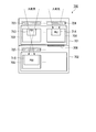
- FIG. 1 is a cross-sectional view showing a cross section of the image sensor 100 according to the first embodiment of the present invention.
- the imaging device 100 includes a first substrate 101, a second substrate 102, a plurality of first pixels 103, a plurality of second pixels 104, and a plurality of third pixels 105.
- the side irradiated with the incident light is the light receiving surface.
- the first substrate 101 and the second substrate 102 are laminated.
- the first substrate 101 and the second substrate 102 are silicon substrates.
- the first substrate 101 transmits a part of the incident light.
- the first pixel 103 is disposed in the first substrate 101.
- the first pixel 103 includes a first photodiode 113 that detects light.
- the first pixel 103 outputs a first signal (W signal, white signal) corresponding to the exposure amount of incident light.
- W signal white signal
- the first pixel 103 is also referred to as a W pixel.
- the second pixel 104 is disposed in the first substrate 101.
- the second pixel 104 includes a second photodiode 114 that detects blue light. Thereby, the second pixel 104 outputs a second signal (B signal, blue signal) corresponding to the exposure amount of the blue light of the incident light.
- B signal blue signal
- the second pixel 104 is also referred to as a B pixel.
- the third pixel 105 is disposed in the second substrate 102.
- the third pixel 105 includes a third photodiode 115 that detects red light. Accordingly, the third pixel 105 outputs a third signal (R signal, red signal) corresponding to the exposure amount of the red light among the incident light transmitted through the first substrate 101.
- the third pixel 105 is also referred to as an R pixel.
- the first photodiode 113 is deeper than the second photodiode. Therefore, the types of light detected by the first photodiode 113 and the second photodiode 114 are different. Further, the depth of the first photodiode 113 is the same as the depth of the third photodiode 115, but the incident light is different, so the light detected by the first photodiode 113 and the third photodiode 115 is different. In the illustrated example, incident light is directly incident on the first photodiode 113. On the other hand, incident light transmitted through the first substrate 101 enters the third photodiode 115.
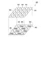
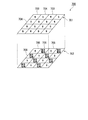
- FIG. 2 is a schematic diagram illustrating an arrangement of the first pixel 103, the second pixel 104, and the third pixel 105 in the present embodiment.
- the first substrate 101 includes eight first pixels 103 and eight second pixels 104 that are regularly arranged in a two-dimensional manner of four rows and four columns. Yes.
- the second substrate 102 includes a total of sixteen third pixels 105 regularly arranged in a two-dimensional manner with 4 rows and 4 columns.
- the first pixels 103 and the second pixels 104 are alternately arranged on the first substrate 101. Further, incident light is directly incident on the first pixel 103 and the second pixel 104. Therefore, the first substrate 101 can output the first signal (W signal) corresponding to the exposure amount of the incident light and the second signal (B signal) corresponding to the exposure amount of the blue light of the incident light. it can.
- the third pixel 105 is arranged on the second substrate 102.
- light that has passed through the first substrate 101 out of incident light is incident on the third pixel 105.
- the first substrate 101 is a silicon substrate and transmits light in a wavelength band including the wavelength of red light. Therefore, the second substrate 102 can output the third signal (R signal) corresponding to the exposure amount of the red light of the incident light.
- the first signal (W signal), the second signal (B signal), and the third signal (R signal) are arranged by the arrangement of the first pixel 103, the second pixel 104, and the third pixel 105. ) Can be output simultaneously.
- the number and arrangement of the first pixels 103 and the second pixels 104 included in the first substrate 101 and the third pixels 105 included in the second substrate 102 are not limited to the example illustrated in FIG. Numbers and sequences may be used.
- the third pixel 105 is disposed below the first pixel 103 and the second pixel 104, but the present invention is not limited thereto.
- the pixel size of the third pixel 105 may be different from the pixel sizes of the first pixel 103 and the second pixel 104 (for example, an integer multiple of the first pixel 103).
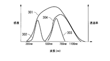
- FIG. 3 is a graph showing the sensitivity of the first pixel 103, the second pixel 104, and the third pixel 105 and the transmittance of the silicon substrate in the present embodiment.
- the horizontal axis of the graph indicates the wavelength (nm).
- the left vertical axis of the graph indicates the sensitivity of the first pixel 103, the second pixel 104, and the third pixel 105.
- the right vertical axis of the graph represents the transmittance of the silicon substrate.
- a line 301 is a line indicating the sensitivity of the first pixel 103 (W pixel).
- the first pixel 103 has a sensitivity corresponding to a wavelength band of 380 nm to 1400 nm.
- the first pixel 103 has a sensitivity corresponding to a wavelength band including the wavelength of red light, the wavelength of green light, and the wavelength of blue light.
- a line 302 is a line indicating the sensitivity of the second pixel 104 (B pixel).
- the second pixel 104 has a sensitivity corresponding to a wavelength band from 380 nm to 500 nm.
- the second pixel 104 has sensitivity according to the wavelength band including the wavelength of blue light.
- a line 303 is a line indicating the sensitivity of the third pixel 105 (R pixel). As shown in the figure, the third pixel 105 has a sensitivity corresponding to a wavelength band of 550 nm to 800 nm. As described above, the third pixel 105 has sensitivity according to the wavelength band including the wavelength of red light.
- the line 304 is a line indicating the transmittance of the silicon substrate.
- the silicon substrate transmits light having a wavelength band of 500 nm to 1500 nm.
- the silicon substrate transmits light in a wavelength band including the wavelength of red light. Therefore, red light out of the incident light passes through the first substrate 101 and enters the second substrate 102. Therefore, even if the first substrate 101 and the second substrate 102 are stacked, the third pixel 105 of the second substrate 102 outputs a third signal (R signal) corresponding to the exposure amount of the red light of the incident light. Can be output. Accordingly, a pixel (for example, the third pixel 105) that detects light having a long wavelength can be used for the second substrate 102.
- the silicon substrate does not transmit light in the wavelength band of blue light. Therefore, even if the second pixel 104 is arranged on the second substrate 102, it is not possible to output the second signal corresponding to the blue light exposure amount of the incident light. Thereby, the pixel (for example, the 2nd pixel 104) which detects light with a short wavelength cannot be used for the 2nd substrate 102.
- FIG. 4 is a block diagram illustrating a configuration of the imaging apparatus 1 in the present embodiment.
- the imaging device 1 includes an imaging element 100 and a signal processing unit 106.
- the image sensor 100 includes a first substrate 101 and a second substrate 102.
- the first substrate 101 includes a first substrate pixel unit 1011.
- the first substrate pixel unit 1011 includes a first substrate pixel 1012 and a first substrate pixel readout circuit 1013.
- the first substrate pixel 1012 includes the plurality of first pixels 103 and the plurality of second pixels 104 described above.
- the second substrate 102 includes a second substrate pixel unit 1021, a driving unit 1024, and a signal reading unit 1025.
- the second substrate pixel unit 1021 includes a second substrate pixel 1022 and a second substrate pixel readout circuit 1023.
- the second substrate pixel 1022 includes the plurality of third pixels 103 described above.
- the driving unit 1024 transmits a control signal to drive the first substrate pixel unit 1011 and the second substrate pixel unit 1021.
- the signal reading unit 1025 includes a circuit that removes signal noise, a circuit that performs A / D conversion, and a scanning circuit.
- the signal readout unit 1025 controls the first substrate pixel readout circuit 1013 to read out the first signal and the second signal from the first substrate pixel 1012.
- the signal readout unit 1025 controls the second substrate pixel readout circuit 1023 to read out the third signal from the second substrate pixel 1022.
- the signal processing unit 106 generates an image using the first signal, the second signal, and the third signal read by the signal reading unit 1025. Specifically, the signal processing unit 106 performs an operation using the first signal (W signal), the second signal (B signal), and the third signal (R signal) to obtain a green light signal (G signal). ) Is generated. Then, the signal processing unit 106 generates an RGB image using the second signal (B signal), the third signal (R signal), and the generated green light signal (G signal). In addition, the signal processing unit 106 generates an NBI image using the second signal (B signal).
- signal transmission between the first substrate 101 and the second substrate 102 may be performed in any manner.
- a through electrode may be provided between the first substrate 101 and the second substrate 102 to transmit a signal between the first substrate 101 and the second substrate 102.
- a transmission path may be provided outside the first substrate 101 and the second substrate 102 to transmit signals between the first substrate 101 and the second substrate 102.
- FIG. 5 is a timing chart showing the drive timing of the image sensor 100 in the present embodiment.
- a timing chart 501 showing driving timings of the first pixel 103 and the second pixel 104 provided on the first substrate 101 and a timing chart showing driving timing of the third pixel 105 provided on the second substrate 102 are shown.
- the horizontal axis of the timing chart is time.
- the charge accumulation time (exposure time) of the third pixel 105 is longer than the charge accumulation time (exposure time) of the first pixel 103 and the second pixel 104.
- the third pixel 105 is irradiated only with the light transmitted through the first substrate 101, and thus the first pixel 103 and the second pixel 104 are irradiated with the amount of light irradiated on the third pixel 105. This is because it is smaller than the amount of light.
- readout is a time for reading out signals from each pixel so that the exposure start timings of the first pixel 103, the second pixel 104, and the third pixel 105 are the same frame start timing. The time is set.
- the first substrate 101 and the second substrate 102 are laminated. Further, the second substrate 102 is disposed at a position overlapping the first substrate 101 and on the side opposite to the light receiving surface side of the first substrate 101 when viewed from the light receiving surface side of the first substrate 101.
- the first substrate 101 transmits light. Further, the light transmitted through the first substrate 101 is irradiated to the second substrate 102.
- the first pixel 103 and the second pixel 104 of the first substrate 101 and the third pixel 105 of the second substrate 102 can be exposed simultaneously. That is, the generation of the first signal by the first pixel 103, the generation of the second signal by the second pixel 104, and the generation of the third signal by the third pixel 105 can be performed simultaneously. Therefore, the signal processing unit 106 is based on the RGB image based on the first signal (W signal), the second signal (B signal), and the third signal (R signal), and the second signal (B signal). Thus, it is possible to simultaneously generate the NBI image subjected to the enhancement process.
- the ratio of the second pixels 104 is a ratio of two pixels to four pixels among the pixels provided in the first substrate 101. Therefore, since more second signals (B signals) can be acquired, the resolution of the NBI image can be improved.
- the green light signal (G signal) is generated using the first signal (W signal), the second signal (B signal), and the third signal (R signal).
- the ratio of the first pixel 103 is a ratio of two pixels to four pixels among the pixels included in the first substrate 101.
- the ratio of the second pixels 104 is a ratio of two pixels to four pixels among the pixels included in the first substrate 101.
- the ratio of the third pixel 105 is all the pixels included in the second substrate 102. Therefore, the resolution of the green light signal (G signal) can be improved, and the resolution of the RGB image can also be improved.
- the first pixel 103, the second pixel 104, and the third pixel 105 generate different types of signals by changing the thickness of the photodiodes 113 to 115 and the incident light.
- the first pixel, the second pixel, and the third pixel may be provided with different color filters to generate different types of signals.
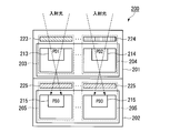
- FIG. 6 is a cross-sectional view showing a cross section of the image sensor 200 including a color filter in which the first pixel 203, the second pixel 204, and the third pixel 205 are different in the present embodiment.
- the imaging device 200 includes a first substrate 201, a second substrate 102, a plurality of first pixels 203, a plurality of second pixels 204, and a plurality of third pixels 205.
- the side irradiated with the incident light is the light receiving surface.
- the first substrate 201 and the second substrate 202 are laminated.
- the first substrate 201 and the second substrate 202 are silicon substrates.
- the first substrate 201 transmits a part of the incident light.
- the first pixel 203 is disposed in the first substrate 201.
- the first pixel 203 includes a first photodiode 213 that detects light and a color filter 223 that transmits light of all wavelengths. Accordingly, the first pixel 203 outputs a first signal (W signal, white signal) corresponding to the exposure amount of incident light.
- the color filter 223 may be one that does not transmit only infrared light.
- the second pixel 204 is disposed in the first substrate 201.
- the second pixel 204 includes a second photodiode 214 that detects light and a color filter 224 that transmits only blue light. Thereby, the second pixel 204 outputs a second signal (B signal, blue signal) corresponding to the exposure amount of the blue light of the incident light.
- the third pixel 205 is disposed in the second substrate 202.
- the third pixel 205 includes a third photodiode 215 that detects light and a color filter 225 that transmits only red light. As a result, the third pixel 205 outputs a third signal (R signal, red signal) corresponding to the exposure amount of the red light out of the incident light transmitted through the first substrate 201.
- the arrangement of the first pixel 203, the second pixel 204, and the third pixel 205 is the same as the arrangement of the first pixel 103, the second pixel 104, and the third pixel 105 shown in FIG. is there. Further, the configuration and operation of the imaging apparatus including the imaging element 200 are the same as the configuration and operation of the imaging apparatus 1 illustrated in FIG.
- the imaging apparatus including the imaging element 200 can simultaneously generate an RGB image and an NBI image that has been enhanced based on the second signal (B signal), as in the imaging apparatus 1 described above. .
- the image pickup apparatus including the image pickup element 200 can improve the resolution of the NBI image, similarly to the image pickup apparatus 1 described above.
- the image pickup apparatus including the image pickup element 200 can improve the resolution of the RGB image similarly to the image pickup apparatus 1 described above.
- the difference between the imaging apparatus in the present embodiment and the imaging apparatus 1 in the first embodiment is the configuration of the imaging element.
- the difference between the image sensor 100 in the first embodiment and the image sensor 400 in the present embodiment is that a circuit unit 406 is provided on the second substrate 402.
- Other configurations and operations are the same as those in the first embodiment.
- FIG. 7 is a cross-sectional view showing a cross section of the image sensor 400 according to the second embodiment of the present invention.
- the imaging device 400 includes a first substrate 401, a second substrate 402, a plurality of first pixels 403, a plurality of second pixels 404, a plurality of third pixels 405, and a circuit unit 406. It has.
- the side irradiated with the incident light is the light receiving surface.
- the first pixel 403 is disposed in the first substrate 401.
- the first pixel 403 includes a first photodiode 413 that detects light and a color filter 423 that transmits light of all wavelengths. Accordingly, the first pixel 403 outputs a first signal (W signal, white signal) corresponding to the exposure amount of incident light.
- the color filter 423 may be one that does not transmit only infrared light.
- the second pixel 404 is disposed in the first substrate 401.
- the second pixel 404 includes a second photodiode 414 that detects light and a color filter 424 that transmits only blue light. Accordingly, the second pixel 404 outputs a second signal (B signal, blue signal) corresponding to the exposure amount of blue light of the incident light.
- the third pixel 405 is disposed in the second substrate 402.
- the third pixel 405 includes a third photodiode 415 that detects light and a color filter 425 that transmits only red light.
- the third pixel 405 outputs a third signal (R signal, red signal) corresponding to the exposure amount of red light out of the incident light transmitted through the first substrate 401.
- the circuit unit 406 includes circuits such as a driving unit 1024 and a signal reading unit 1025. Accordingly, circuits such as the driving unit 1024 and the signal reading unit 1025 can be arranged in the circuit unit 406.
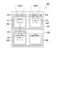
- FIG. 8 is a schematic diagram illustrating an arrangement of the first pixel 403, the second pixel 404, the third pixel 405, and the circuit unit 406 in the present embodiment.
- the first substrate 401 includes eight first pixels 403 and eight second pixels 404 regularly arranged in a two-dimensional manner of 4 rows and 4 columns. Yes.
- the second substrate 402 includes eight third pixels 405 regularly arranged in a two-dimensional manner of 4 rows and 4 columns, and eight circuit units 406.
- the first substrate 401 can output the first signal (W signal) corresponding to the exposure amount of the incident light and the second signal (B signal) corresponding to the exposure amount of the blue light of the incident light. it can.
- the third pixels 405 and the circuit units 406 are alternately arranged on the second substrate 402. Further, the third pixel 405 is disposed at a position where the light transmitted through the first pixel 403 is incident. That is, the third pixel 405 is disposed below the first pixel 403. The circuit unit 406 is disposed below the second pixel 404.
- the color filter 423 included in the first pixel 403 transmits all light.
- the first substrate 401 is a silicon substrate and transmits light in a wavelength band including the wavelength of red light. Therefore, the third pixel 405 of the second substrate 402 can output the third signal (R signal) corresponding to the exposure amount of the red light of the incident light.
- the color filter 424 included in the second pixel 404 transmits only blue light. That is, it does not transmit red light. Accordingly, red light is not included in the light transmitted through the second pixel 404. Therefore, even if the third pixel 405 is disposed under the second pixel 404, it is difficult to detect red light with high accuracy. Further, for example, when a circuit such as the driving unit 1024, the signal reading unit 1025, or the second substrate pixel reading circuit 1023 is arranged around the third pixel 405, the aperture ratio of the third pixel 405 is decreased, and the third signal It is conceivable that the S / N ratio decreases.
- the driving unit 1024, the signal readout unit 1025, the second substrate pixel readout circuit 1023, and the like are arranged as the circuit unit 406 under the second pixel 404 that does not transmit red light.
- the aperture ratio of the three pixels 405 can be increased. Therefore, the S / N ratio of the third signal output from the third pixel 405 can be increased.
- the number and arrangement of the first pixels 403 and the second pixels 404 included in the first substrate 401 and the third pixels 405 and the circuit units 406 included in the second substrate 402 are not limited to the example illustrated in FIG. Any number and arrangement.
- the third pixel 405 is disposed below the first pixel 403, but the present invention is not limited to this.
- the pixel size of the third pixel 405 may be different from the pixel size of the first pixel 403 (for example, an integer multiple of the first pixel 403).
- the configuration and operation of the imaging apparatus including the imaging element 400 are the same as those of the imaging apparatus 1 in the first embodiment.
- the RGB image generation method and the NBI image generation method by the signal processing unit 106 are the same as those in the first embodiment.
- the difference between the imaging device in the present embodiment and the imaging device in the second embodiment is the configuration of the imaging device.
- the difference between the image sensor 400 in the second embodiment and the image sensor 600 in the present embodiment is the number and arrangement of the circuit units 606 provided on the second substrate 602. Other configurations are the same as those of the second embodiment.
- FIG. 9 is a schematic diagram showing an arrangement of the first pixel 603, the second pixel 604, the third pixel 605, and the circuit unit 606 in the present embodiment.
- the first substrate 601 includes eight first pixels 603 and eight second pixels 604 that are regularly arranged in a two-dimensional manner in four rows and four columns. Yes.
- the second substrate 602 includes four third pixels 605 regularly arranged in a two-dimensional form of 4 rows and 4 columns, and 12 circuit units 606.
- first pixels 603 and second pixels 604 are alternately arranged. Further, incident light is directly incident on the first pixel 603 and the second pixel 604. Therefore, the first substrate 601 can output the first signal (W signal) corresponding to the exposure amount of incident light and the second signal (B signal) corresponding to the exposure amount of blue light of the incident light. it can.
- the third pixels 605 and the circuit portions 606 are alternately arranged on the odd-numbered rows of the second substrate 602.
- a circuit portion 606 is arranged on even-numbered rows of the second substrate 602.
- the third pixel 605 is disposed at a position where the light transmitted through the first pixel 603 is incident. That is, the third pixel 605 is disposed below the first pixel 603.
- the color filter included in the first pixel 603 (same as the color filter 423 of the second embodiment) transmits all light.
- the first substrate 601 is a silicon substrate and transmits light in a wavelength band including the wavelength of red light. Therefore, the third pixel 605 of the second substrate 602 can output the third signal (R signal) corresponding to the exposure amount of the red light of the incident light.
- the first substrate pixel readout circuit 1013 arranged on the first substrate 601 is replaced with the circuit unit 606. Can be arranged. Accordingly, it is not necessary to arrange the first substrate pixel readout circuit 1013 on the first substrate 601, and the aperture ratio between the first pixel 603 and the second pixel 604 can be increased. Therefore, the S / N between the first signal output from the first pixel 603 and the second signal output from the second pixel 604 can be increased.
- the number and arrangement of the first pixels 603 and the second pixels 604 included in the first substrate 601 and the third pixels 605 and the circuit units 606 included in the second substrate 602 are not limited to the example illustrated in FIG. Any number and arrangement.
- the third pixel 605 is disposed below the first pixel 603, but this is not restrictive.
- the pixel size of the third pixel 605 may be different from the pixel size of the first pixel 603 (for example, an integer multiple of the first pixel 603).
- the configuration and operation of the imaging apparatus including the imaging element 600 are the same as those of the imaging apparatus in the second embodiment.
- the RGB image generation method and the NBI image generation method by the signal processing unit 106 are the same as those in the second embodiment.
- the difference between the imaging apparatus in the present embodiment and the imaging apparatus 1 in the first embodiment is the configuration of the imaging element.
- the difference between the image sensor 100 in the first embodiment and the image sensor 700 in the present embodiment is that a bonding electrode 706 is provided between the first substrate 701 and the second substrate 702, and the bonding of the second substrate 702 is performed.
- the third pixel 705 is not provided at a place where the electrode 706 is provided.
- Other configurations and operations are the same as those in the first embodiment.
- FIG. 10 is a cross-sectional view showing a cross section of an image sensor 700 according to the fourth embodiment of the present invention.
- the image sensor 700 includes a first substrate 701, a second substrate 702, a plurality of first pixels 703, a plurality of second pixels 704, a plurality of third pixels 705, and a bonding electrode 706. It has.
- the side irradiated with the incident light is the light receiving surface.
- the first pixel 703 is disposed in the first substrate 701.
- the first pixel 703 includes a first photodiode 713 that detects light and a color filter 723 that transmits light of all wavelengths. Accordingly, the first pixel 703 outputs a first signal (W signal, white signal) corresponding to the exposure amount of incident light.
- the color filter 423 may be one that does not transmit only infrared light.
- the second pixel 704 is disposed in the first substrate 701.
- the second pixel 704 includes a second photodiode 714 that detects light and a color filter 724 that transmits only blue light. As a result, the second pixel 704 outputs a second signal (B signal, blue signal) corresponding to the exposure amount of the blue light of the incident light.
- the third pixel 705 is disposed in the second substrate 702.
- the third pixel 705 includes a third photodiode 715 that detects light and a color filter 725 that transmits only red light.
- the third pixel 705 outputs a third signal (R signal, red signal) corresponding to the exposure amount of the red light out of the incident light transmitted through the first substrate 701.
- the bonding electrode 706 transmits a signal between the first substrate 701 and the second substrate 702. Accordingly, signal transmission can be performed between the first substrate 701 and the second substrate 702.
- FIG. 11 is a schematic diagram illustrating an arrangement of the first pixel 703, the second pixel 704, the third pixel 705, and the bonding electrode 706 in the present embodiment.
- the first substrate 701 includes eight first pixels 703 and eight second pixels 704 regularly arranged in a two-dimensional manner of 4 rows and 4 columns. Yes.
- the second substrate 702 includes eight third pixels 705 regularly arranged in a two-dimensional manner with 4 rows and 4 columns, and eight junction electrodes 706.
- first pixels 703 and second pixels 704 are alternately arranged. Further, incident light is directly incident on the first pixel 703 and the second pixel 704. Therefore, the first substrate 701 can output the first signal (W signal) corresponding to the exposure amount of incident light and the second signal (B signal) corresponding to the exposure amount of blue light of the incident light. it can.
- the third pixels 705 and the bonding electrodes 706 are alternately arranged.
- the third pixel 705 is arranged at a position where light transmitted through the first pixel 703 is incident. That is, the third pixel 705 is disposed below the first pixel 703.
- the bonding electrode 706 is disposed below the second pixel 704.
- the first substrate 701 is a silicon substrate and transmits light in a wavelength band including the wavelength of red light. Therefore, the third pixel 705 of the second substrate 702 can output a third signal (R signal) corresponding to the exposure amount of red light of incident light.
- the color filter 724 included in the second pixel 704 transmits only blue light. That is, it does not transmit red light. Therefore, red light is not included in the light transmitted through the second pixel 704. Therefore, even if the third pixel 705 is disposed under the second pixel 704, it is difficult to detect red light with high accuracy.
- the opening of the third pixel 705 is opened. It is conceivable that the rate decreases. Further, when the aperture ratio of the third pixel 705 decreases, it is conceivable that the S / N of the third signal output from the third pixel 705 decreases.
- the aperture ratio of the third pixel 705 can be increased by disposing the bonding electrode 706 under the second pixel 704 that does not transmit red light. Therefore, the S / N ratio of the third signal output from the third pixel 705 can be increased.
- the number and arrangement of the first pixel 703 and the second pixel 704 included in the first substrate 701 and the third pixel 705 and the bonding electrode 706 included in the second substrate 702 are not limited to the example illustrated in FIG. Any number and arrangement.
- the third pixel 705 is disposed below the first pixel 703.
- the present invention is not limited to this.
- the pixel size of the third pixel 705 may be different from the pixel size of the first pixel 703 (for example, an integer multiple of the first pixel 703).
- the configuration and operation of the imaging apparatus including the imaging element 700 are the same as those of the imaging apparatus 1 in the first embodiment.
- the RGB image generation method and the NBI image generation method by the signal processing unit 106 are the same as those in the first embodiment.
- the difference between the imaging apparatus in the present embodiment and the imaging apparatus 1 in the first embodiment is the configuration of the imaging element.
- the difference between the image sensor 100 according to the first embodiment and the image sensor 800 according to the present embodiment is that a fourth signal (G signal, green signal) corresponding to the exposure amount of green light of incident light is applied to the first substrate 801. ) Is provided, the fourth pixel 806 is provided.
- Other configurations are the same as those of the first embodiment.
- the fourth pixel 806 may include a photodiode that detects green light, so that a fourth signal corresponding to the exposure amount of the green light in the incident light may be output.
- the fourth pixel 806 includes a photodiode that detects light and a color filter that transmits only green light, so that a fourth signal corresponding to the exposure amount of green light in incident light is output. May be.
- FIG. 12 is a schematic diagram showing an arrangement of the first pixel 803, the second pixel 804, the third pixel 805, and the fourth pixel 806 in the present embodiment.
- the first substrate 801 has four first pixels 803, eight second pixels 804, and four pieces arranged regularly in a two-dimensional manner in four rows and four columns.
- a third pixel 806 is included.
- the second substrate 802 includes 16 third pixels 405 regularly arranged in a two-dimensional manner of 4 rows and 4 columns.
- the first pixels 803 and the second pixels 804 are alternately arranged in the odd-numbered rows of the first substrate 801. Further, the second pixels 804 and the fourth pixels 806 are alternately arranged on the even-numbered rows of the first substrate 802. Further, incident light is directly incident on the first pixel 803, the second pixel 804, and the fourth pixel 805. Therefore, in the first substrate 801, the first signal (W signal) corresponding to the exposure amount of the incident light, the second signal (B signal) corresponding to the exposure amount of the blue light of the incident light, and the incident light A fourth signal (G signal) corresponding to the amount of green light exposure can be output.
- the third pixel 805 is disposed on the second substrate 802.
- light transmitted through the first substrate 801 is incident on the third pixel 805.
- the first substrate 801 is a silicon substrate and transmits light in a wavelength band including the wavelength of red light. Therefore, the second substrate 802 can output the third signal (R signal) corresponding to the exposure amount of the red light of the incident light.
- the arrangement of the first pixel 803, the second pixel 804, the third pixel 805, and the fourth pixel 806, the first signal (W signal), the second signal (B signal), The third signal (R signal) and the fourth signal (G signal) can be output simultaneously.
- the number and arrangement of the first pixel 803, the second pixel 804, the fourth pixel 806, and the third pixel 805 included in the second substrate 802 included in the first substrate 801 are the examples illustrated in FIG. The number and arrangement are not limited to these.
- the third pixel 805 is disposed below the first pixel 803, the second pixel 804, and the fourth pixel 806.
- the present invention is not limited to this.
- the pixel size of the third pixel 805 is set to a size different from the pixel sizes of the first pixel 803, the second pixel 804, and the fourth pixel 806 (for example, an integer multiple of the first pixel 803). Can also be devised.
- the signal processing unit 106 generates an image using the second signal, the third signal, and the fourth signal read by the signal reading unit 1025. Specifically, the signal processing unit 106 generates an RGB image using the second signal (B signal), the third signal (R signal), and the fourth signal (G signal). In addition, the signal processing unit 106 generates an NBI image using the second signal (B signal).
- a green light signal (G signal) may be generated by calculating using the first signal (W signal), the second signal (B signal), and the third signal (R signal). Then, both the generated green light signal (G signal) and the fourth signal (G signal) may be used to generate an RGB image.
- the G signal (fourth signal) can be obtained without performing signal processing. Further, since the G signal can be obtained without performing signal processing, an RGB image with higher color reproducibility can be obtained.
- the difference between the imaging apparatus in the present embodiment and the imaging apparatus 1 in the first embodiment is the configuration of the imaging element.
- the difference between the image sensor 100 in the first embodiment and the image sensor 900 in the present embodiment is that a fifth signal (Y signal, yellow signal) corresponding to the exposure amount of yellow light of incident light is applied to the first substrate 901. ) Is provided in place of the first pixel 103.
- Other configurations are the same as those of the first embodiment.
- the fifth pixel 906 may include a photodiode that detects yellow light, and may output a fifth signal corresponding to the exposure amount of yellow light in the incident light.
- the fifth pixel 906 includes a photodiode that detects light and a color filter that transmits only yellow light, so that a fifth signal corresponding to the exposure amount of yellow light in incident light is output. May be.
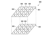
- FIG. 13 is a schematic diagram showing an arrangement of the second pixel 904, the third pixel 905, and the fifth pixel 906 in the present embodiment.
- the first substrate 901 includes eight fourth pixels 906 and eight second pixels 904 regularly arranged in a two-dimensional manner of 4 rows and 4 columns. Yes.
- the second substrate 902 includes 16 third pixels 905 regularly arranged in a two-dimensional manner of 4 rows and 4 columns.
- the fifth pixels 906 and the second pixels 904 are alternately arranged. Further, incident light is directly incident on the fifth pixel 906 and the second pixel 904. Therefore, in the first substrate 901, the fifth signal (Y signal) corresponding to the yellow light exposure amount of the incident light and the second signal (B signal) corresponding to the blue light exposure amount of the incident light are generated. Can be output.
- the third pixel 905 is disposed on the second substrate 902.
- light transmitted through the first substrate 901 out of incident light is incident on the third pixel 905.
- the first substrate 901 is a silicon substrate and transmits light in a wavelength band including the wavelength of red light. Therefore, the second substrate 902 can output the third signal (R signal) corresponding to the exposure amount of the red light of the incident light.
- the second signal (B signal), the third signal (R signal), and the fifth signal (Y signal) are arranged by the arrangement of the second pixel 904, the third pixel 905, and the fifth pixel 906. ) Can be output simultaneously.
- the number and arrangement of the fifth pixels 906 and the second pixels 904 included in the first substrate 901 and the third pixels 905 included in the second substrate 902 are not limited to the example illustrated in FIG. Numbers and sequences may be used.
- the third pixel 905 is disposed below the fifth pixel 906 and the second pixel 904, but the present invention is not limited thereto.
- the pixel size of the third pixel 905 may be different from the pixel sizes of the fifth pixel 906 and the second pixel 904 (for example, an integer multiple of the fifth pixel 906).
- the signal processing unit 106 generates an image using the second signal, the third signal, and the fifth signal read by the signal reading unit 1025. Specifically, the signal processing unit 106 performs an operation using the third signal (R signal) and the fifth signal (Y signal) to generate a green light signal (G signal). Then, the signal processing unit 106 generates an RGB image using the second signal (B signal), the third signal (R signal), and the generated green light signal (G signal). In addition, the signal processing unit 106 generates an NBI image using the second signal (B signal).
- both the RGB image and the NBI image can be generated simultaneously.
- an imaging device 3000 (endoscope type) incorporating any one of the imaging devices 100, 200, 400, 600, 700, 800, 900 described in the first to sixth embodiments.
- An imaging device and an endoscope device will be described.
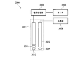
- FIG. 14 is a block diagram illustrating a configuration of the imaging apparatus 3000 according to the present embodiment.
- the imaging device 3000 includes an endoscope scope 3001, a signal processing unit 3002, a monitor 3003, and a light source unit 3004.
- the signal processing unit 3002 generates an RGB image and an NBI image.
- the signal processing unit 3002 controls each unit of the imaging apparatus 3000.
- the monitor 3003 is a liquid crystal display, for example, and displays an image.
- the light source unit 3004 is an LED, for example, and emits light.
- the endoscope scope 3001 includes an imaging element 3011, an imaging lens 3012, a light guide 3013, and an illumination lens 3014.
- the image sensor 3011 is one of the image sensors 100, 200, 400, 600, 700, 800, and 900 described in the first to fourth embodiments.
- the image sensor 3011 is disposed at the distal end portion of the endoscope scope 3001.
- the imaging lens 3012 is disposed on the light receiving surface side of the imaging element 3011.
- the illumination lens 3014 is disposed at the distal end portion of the endoscope scope 3001.
- the light guide 3013 irradiates the illumination lens 3014 with light emitted from the light source unit 3004.
- the illumination lens 3014 collects the light emitted from the light guide 3013 and irradiates the subject.
- the imaging lens 3012 collects light from the subject and irradiates the imaging element 3011.
- the imaging element 3011 outputs a signal based on the light irradiated by the imaging lens 3012.
- the signal processing unit 3002 generates an RGB image and an NBI image based on the signal generated by the image sensor 3011.
- the RGB image and NBI image generation methods are the same as the methods described in the first to sixth embodiments.
- a monitor 3003 displays an RGB image, an NBI image, or the like generated by the signal processing unit 3002.
- the image sensor 100, 200, 400, 600, 700, 800, 900 described in the first to sixth embodiments can simultaneously capture a highly accurate RGB image and an NBI image. Therefore, by using any of the imaging devices 100, 200, 400, 600, 700, 800, and 900 described in the first to sixth embodiments for the imaging device 3000, a highly accurate RGB image and NBI can be obtained. Images can be taken simultaneously. For example, highly accurate RGB images and NBI images can be used for cancer observation and the like.
- the state of the capillary can be observed more clearly.
Landscapes
- Health & Medical Sciences (AREA)
- Engineering & Computer Science (AREA)
- Life Sciences & Earth Sciences (AREA)
- Signal Processing (AREA)
- Multimedia (AREA)
- Physics & Mathematics (AREA)
- Surgery (AREA)
- Spectroscopy & Molecular Physics (AREA)
- Public Health (AREA)
- Biomedical Technology (AREA)
- Medical Informatics (AREA)
- Molecular Biology (AREA)
- Biophysics (AREA)
- Animal Behavior & Ethology (AREA)
- General Health & Medical Sciences (AREA)
- Pathology (AREA)
- Heart & Thoracic Surgery (AREA)
- Veterinary Medicine (AREA)
- Optics & Photonics (AREA)
- Nuclear Medicine, Radiotherapy & Molecular Imaging (AREA)
- Radiology & Medical Imaging (AREA)
- Cardiology (AREA)
- Physiology (AREA)
- Color Television Image Signal Generators (AREA)
- Transforming Light Signals Into Electric Signals (AREA)
- Solid State Image Pick-Up Elements (AREA)
Abstract
Description
図1は、本発明の第1の実施形態における撮像素子100の断面を示した断面図である。図示する例では、撮像素子100は、第1基板101と、第2基板102と、複数の第1画素103と、複数の第2画素104と、複数の第3画素105とを備えている。また、入射光が照射される側を受光面とする。
次に、本発明の第2の実施形態について説明する。本実施形態における撮像装置と、第1の実施形態における撮像装置1とで異なる点は、撮像素子の構成である。第1の実施形態における撮像素子100と本実施形態における撮像素子400とで異なる点は、第2基板402に回路部406が設けられている点である。その他の構成および動作は、第1の実施形態と同様である。
次に、本発明の第3の実施形態について説明する。本実施形態における撮像装置と、第2の実施形態における撮像装置とで異なる点は、撮像素子の構成である。第2の実施形態における撮像素子400と本実施形態における撮像素子600とで異なる点は、第2基板602に設けられる回路部606の数および配列である。なお、その他の構成は、第2の実施形態と同様である。
次に、本発明の第4の実施形態について説明する。本実施形態における撮像装置と、第1の実施形態における撮像装置1とで異なる点は、撮像素子の構成である。第1の実施形態における撮像素子100と本実施形態における撮像素子700とで異なる点は、第1基板701と第2基板702との間に接合電極706が設けられ、第2基板702のうち接合電極706が設けられている箇所には第3画素705が設けられていない点である。その他の構成および動作は、第1の実施形態と同様である。
次に、本発明の第5の実施形態について説明する。本実施形態における撮像装置と、第1の実施形態における撮像装置1とで異なる点は、撮像素子の構成である。第1の実施形態における撮像素子100と本実施形態における撮像素子800とで異なる点は、第1基板801に、入射光のうち緑色光の露光量に応じた第4信号(G信号、グリーン信号)を出力する第4画素806が設けられている点である。その他の構成は、第1の実施形態と同様である。
次に、本発明の第6の実施形態について説明する。本実施形態における撮像装置と、第1の実施形態における撮像装置1とで異なる点は、撮像素子の構成である。第1の実施形態における撮像素子100と本実施形態における撮像素子900とで異なる点は、第1基板901に、入射光のうち黄色光の露光量に応じた第5信号(Y信号、イエロー信号)を出力する第5画素906が、第1画素103の代わりに設けられている点である。その他の構成は、第1の実施形態と同様である。
次に、本発明の第7の実施形態について説明する。本実施形態では、第1の実施形態~第6の実施形態に記載した撮像素子100,200,400,600,700,800,900のうち、いずれかを内蔵した撮像装置3000(内視鏡型撮像装置、内視鏡装置)について説明する。
また、本発明は前述した説明によって限定されることはなく、添付のクレームの範囲によってのみ限定される。
Claims (6)
- 複数の第1画素と複数の第2画素とを有する第1基板と、
複数の第3画素を有し、前記第1基板に対向する第2基板と、
信号を生成する処理部と、
を備え、
前記複数の第3画素は、前記複数の第1画素の透過光を受光し、
前記複数の第1画素は、緑色光の波長を含む波長帯域に応じた信号を出力し、赤色光の波長を含む波長帯域を透過し、
前記複数の第2画素は、青色光の波長を含み、赤色光の波長と緑色光の波長とを含まない波長帯域に応じた信号を出力し、
前記複数の第3画素は、赤色光の波長を含む波長帯域に応じた信号を出力し、
前記複数の第1の画素と前記複数の第2の画素とは互いに対応しており、
前記処理部は、少なくとも前記複数の第1画素の出力と前記複数の第3画素の出力から、緑色光の波長を含み、青色光の波長と赤色光の波長とを含まない波長帯域に応じた信号を生成する
撮像装置。 - 前記複数の第2画素に対応する領域には複数の回路領域が配置され、
前記複数の回路領域は、少なくとも前記複数の第3画素の読出しを行う
請求項1に記載の撮像装置。 - 前記複数の回路領域は、前記複数の第1画素および前記複数の第2画素の読出しを行う
請求項2に記載の撮像装置。 - 前記複数の第1画素は、緑色光の波長および青色光の波長とを含む波長帯域に応じた信号を出力し、赤い露光の波長を含む波長帯域を透過する
請求項1に記載の撮像装置。 - 前記複数の第1画素は、緑色光の波長を含み、青色光の波長を含まない波長帯域に応じた信号を出力し、赤色光の波長を含む波長帯域を透過する
請求項1に記載の撮像装置。 - 狭帯域光を照射することにより、粘膜表層の毛細血管を強調表示して観察する撮像装置であって、
前記第1基板が有する前記複数の第1画素と前記複数の第2画素とが出力した信号から第1画像を作成し、
前記第2基板が有する前記複数の第3が出力した信号から第2画像を作成する
請求項1に記載の撮像装置。
Priority Applications (5)
| Application Number | Priority Date | Filing Date | Title |
|---|---|---|---|
| CN201580079231.9A CN107534760B (zh) | 2015-05-01 | 2015-05-01 | 摄像装置 |
| PCT/JP2015/063073 WO2016178266A1 (ja) | 2015-05-01 | 2015-05-01 | 撮像装置 |
| JP2017516232A JPWO2016178266A1 (ja) | 2015-05-01 | 2015-05-01 | 撮像装置 |
| DE112015006389.7T DE112015006389T5 (de) | 2015-05-01 | 2015-05-01 | Bildgebungsvorrichtung |
| US15/797,469 US10602919B2 (en) | 2015-05-01 | 2017-10-30 | Imaging device |
Applications Claiming Priority (1)
| Application Number | Priority Date | Filing Date | Title |
|---|---|---|---|
| PCT/JP2015/063073 WO2016178266A1 (ja) | 2015-05-01 | 2015-05-01 | 撮像装置 |
Related Child Applications (1)
| Application Number | Title | Priority Date | Filing Date |
|---|---|---|---|
| US15/797,469 Continuation US10602919B2 (en) | 2015-05-01 | 2017-10-30 | Imaging device |
Publications (1)
| Publication Number | Publication Date |
|---|---|
| WO2016178266A1 true WO2016178266A1 (ja) | 2016-11-10 |
Family
ID=57218540
Family Applications (1)
| Application Number | Title | Priority Date | Filing Date |
|---|---|---|---|
| PCT/JP2015/063073 Ceased WO2016178266A1 (ja) | 2015-05-01 | 2015-05-01 | 撮像装置 |
Country Status (5)
| Country | Link |
|---|---|
| US (1) | US10602919B2 (ja) |
| JP (1) | JPWO2016178266A1 (ja) |
| CN (1) | CN107534760B (ja) |
| DE (1) | DE112015006389T5 (ja) |
| WO (1) | WO2016178266A1 (ja) |
Cited By (2)
| Publication number | Priority date | Publication date | Assignee | Title |
|---|---|---|---|---|
| JP2018085645A (ja) * | 2016-11-24 | 2018-05-31 | キヤノン株式会社 | 撮像装置、撮像システム、および、移動体 |
| WO2024075253A1 (ja) * | 2022-10-06 | 2024-04-11 | ソニーセミコンダクタソリューションズ株式会社 | 光検出装置および電子機器 |
Families Citing this family (4)
| Publication number | Priority date | Publication date | Assignee | Title |
|---|---|---|---|---|
| JP6561571B2 (ja) * | 2015-05-12 | 2019-08-21 | ソニー株式会社 | 医療用撮像装置、撮像方法及び撮像装置 |
| WO2018225122A1 (ja) * | 2017-06-05 | 2018-12-13 | オリンパス株式会社 | 内視鏡装置 |
| CN110246858A (zh) * | 2019-06-21 | 2019-09-17 | 芯盟科技有限公司 | 图像传感器及其形成方法 |
| US12148775B2 (en) * | 2020-10-13 | 2024-11-19 | Samsung Electronics Co., Ltd. | Hyperspectral element, hyperspectral sensor including the same, and hyperspectral image generating apparatus |
Citations (3)
| Publication number | Priority date | Publication date | Assignee | Title |
|---|---|---|---|---|
| JP2009272620A (ja) * | 2008-05-09 | 2009-11-19 | Samsung Electronics Co Ltd | 積層型イメージセンサー |
| JP2014064196A (ja) * | 2012-09-21 | 2014-04-10 | Olympus Corp | 撮像装置 |
| JP2014135535A (ja) * | 2013-01-08 | 2014-07-24 | Olympus Corp | 撮像装置 |
Family Cites Families (3)
| Publication number | Priority date | Publication date | Assignee | Title |
|---|---|---|---|---|
| US20060232668A1 (en) | 2005-04-18 | 2006-10-19 | Given Imaging Ltd. | Color filter array with blue elements |
| CA2835870A1 (en) * | 2011-05-12 | 2012-11-15 | Olive Medical Corporation | Pixel array area optimization using stacking scheme for hybrid image sensor with minimal vertical interconnects |
| JP5715602B2 (ja) * | 2012-09-07 | 2015-05-07 | 富士フイルム株式会社 | 内視鏡システム及び内視鏡システムの作動方法 |
-
2015
- 2015-05-01 JP JP2017516232A patent/JPWO2016178266A1/ja not_active Ceased
- 2015-05-01 CN CN201580079231.9A patent/CN107534760B/zh not_active Expired - Fee Related
- 2015-05-01 WO PCT/JP2015/063073 patent/WO2016178266A1/ja not_active Ceased
- 2015-05-01 DE DE112015006389.7T patent/DE112015006389T5/de not_active Withdrawn
-
2017
- 2017-10-30 US US15/797,469 patent/US10602919B2/en active Active
Patent Citations (3)
| Publication number | Priority date | Publication date | Assignee | Title |
|---|---|---|---|---|
| JP2009272620A (ja) * | 2008-05-09 | 2009-11-19 | Samsung Electronics Co Ltd | 積層型イメージセンサー |
| JP2014064196A (ja) * | 2012-09-21 | 2014-04-10 | Olympus Corp | 撮像装置 |
| JP2014135535A (ja) * | 2013-01-08 | 2014-07-24 | Olympus Corp | 撮像装置 |
Cited By (2)
| Publication number | Priority date | Publication date | Assignee | Title |
|---|---|---|---|---|
| JP2018085645A (ja) * | 2016-11-24 | 2018-05-31 | キヤノン株式会社 | 撮像装置、撮像システム、および、移動体 |
| WO2024075253A1 (ja) * | 2022-10-06 | 2024-04-11 | ソニーセミコンダクタソリューションズ株式会社 | 光検出装置および電子機器 |
Also Published As
| Publication number | Publication date |
|---|---|
| JPWO2016178266A1 (ja) | 2018-02-22 |
| CN107534760B (zh) | 2019-06-07 |
| DE112015006389T5 (de) | 2017-12-28 |
| CN107534760A (zh) | 2018-01-02 |
| US10602919B2 (en) | 2020-03-31 |
| US20180049633A1 (en) | 2018-02-22 |
Similar Documents
| Publication | Publication Date | Title |
|---|---|---|
| US10602919B2 (en) | Imaging device | |
| JP7314976B2 (ja) | 撮像装置及び撮像方法 | |
| US10335019B2 (en) | Image pickup element and endoscope device | |
| JP6027832B2 (ja) | 撮像装置 | |
| JP6076093B2 (ja) | 撮像装置 | |
| CN102547109B (zh) | 成像装置和成像设备 | |
| JP4957413B2 (ja) | 固体撮像素子及びこれを用いた撮像装置 | |
| JPWO2018008062A1 (ja) | 蛍光観察装置および蛍光観察内視鏡装置 | |
| JP2013045917A (ja) | 撮像素子、撮像装置及び生体撮像装置 | |
| WO2016129062A1 (ja) | 画像処理装置、内視鏡システム、撮像装置、画像処理方法およびプログラム | |
| JP5698874B2 (ja) | カラー撮像素子及び撮像装置 | |
| JPWO2017064760A1 (ja) | 積層型撮像素子、画像処理装置、画像処理方法およびプログラム | |
| US10516866B2 (en) | Imaging device and endoscope device | |
| WO2016051594A1 (ja) | 固体撮像装置および撮像装置 | |
| JP4694310B2 (ja) | 電子内視鏡、内視鏡光源装置、内視鏡プロセッサ、および内視鏡システム | |
| US20150077600A1 (en) | Color filter array and solid-state image sensor | |
| JP6153689B1 (ja) | 撮像素子及び撮像装置 | |
| JP2008283057A (ja) | 固体撮像素子およびそれを用いる撮像装置 | |
| WO2016163242A1 (ja) | 固体撮像素子および電子機器 | |
| JP6277138B2 (ja) | 内視鏡システム及びその作動方法 | |
| JP6589071B2 (ja) | 撮像装置、内視鏡および内視鏡システム | |
| JP2013178341A (ja) | 撮像装置およびデジタルカメラ |
Legal Events
| Date | Code | Title | Description |
|---|---|---|---|
| 121 | Ep: the epo has been informed by wipo that ep was designated in this application |
Ref document number: 15891273 Country of ref document: EP Kind code of ref document: A1 |
|
| ENP | Entry into the national phase |
Ref document number: 2017516232 Country of ref document: JP Kind code of ref document: A |
|
| WWE | Wipo information: entry into national phase |
Ref document number: 112015006389 Country of ref document: DE |
|
| 122 | Ep: pct application non-entry in european phase |
Ref document number: 15891273 Country of ref document: EP Kind code of ref document: A1 |