WO2016175195A1 - グラフェンおよび電子素子ならびにこれらの製造方法 - Google Patents
グラフェンおよび電子素子ならびにこれらの製造方法 Download PDFInfo
- Publication number
- WO2016175195A1 WO2016175195A1 PCT/JP2016/063014 JP2016063014W WO2016175195A1 WO 2016175195 A1 WO2016175195 A1 WO 2016175195A1 JP 2016063014 W JP2016063014 W JP 2016063014W WO 2016175195 A1 WO2016175195 A1 WO 2016175195A1
- Authority
- WO
- WIPO (PCT)
- Prior art keywords
- graphene
- substrate
- metal
- carbon
- main surface
- Prior art date
- Legal status (The legal status is an assumption and is not a legal conclusion. Google has not performed a legal analysis and makes no representation as to the accuracy of the status listed.)
- Ceased
Links
Images




Classifications
-
- H—ELECTRICITY
- H10—SEMICONDUCTOR DEVICES; ELECTRIC SOLID-STATE DEVICES NOT OTHERWISE PROVIDED FOR
- H10K—ORGANIC ELECTRIC SOLID-STATE DEVICES
- H10K10/00—Organic devices specially adapted for rectifying, amplifying, oscillating or switching; Organic capacitors or resistors having potential barriers
- H10K10/40—Organic transistors
- H10K10/46—Field-effect transistors, e.g. organic thin-film transistors [OTFT]
-
- C—CHEMISTRY; METALLURGY
- C01—INORGANIC CHEMISTRY
- C01B—NON-METALLIC ELEMENTS; COMPOUNDS THEREOF; METALLOIDS OR COMPOUNDS THEREOF NOT COVERED BY SUBCLASS C01C
- C01B32/00—Carbon; Compounds thereof
- C01B32/05—Preparation or purification of carbon not covered by groups C01B32/15, C01B32/20, C01B32/25, C01B32/30
Definitions
- the present invention relates to a graphene production technique, and more particularly to a technique for producing large-area and high-quality single-layer graphene at low temperatures and a technique for applying such graphene to an electronic device.
- Graphene has various specific properties due to its ideal two-dimensional structure, such as good conductivity and high electron / hole mobility.
- inelastic electron conductivity, spin conductivity, mechanical strength, light absorption and emission, heat conduction, and other properties have attracted attention, and are expected to be industrially applied in various fields. It is.
- the first discovery of graphene was by Novoselov et al. This graphene was obtained by peeling pyrolytic graphite crystals with a scotch tape and transferring them to a Si substrate. Although the size of the graphene crystal is about several microns, it is characterized in that a graphene film can be easily obtained with relatively high reproducibility (Non-Patent Documents 1 and 2).
- the silicon carbide crystal is vacuum-heated at about 2000 ° C. to evaporate the Si element on the surface (silicon sublimation), thereby forming a graphene crystal layer on the silicon carbide surface (Non-Patent Documents 3 to 7). ).
- a graphene film is formed by growing a hydrocarbon gas as a raw material on the surface of a metal crystal such as nickel or iron by a thermal CVD method (Non-Patent Documents 8 and 9).
- Non-patent Document 10 Non-patent Document 10
- Non-Patent Document 11 Single-layer graphene can be obtained even at a relatively low substrate temperature of about 600 ° C.
- the Raman scattering spectrum of the obtained graphene is 1300 cm ⁇ . A very strong D peak due to defects appearing in the vicinity of 1 is observed.
- the substrate temperature decreases, a large amount of fine graphene nuclei are generated, and as a result, when the synthesized graphene film is viewed microscopically, grain boundaries exist at high density, which significantly reduces electron mobility. I will let you.
- Patent Document 1 a method for producing a graphene film that can produce large-area graphene without requiring high temperature.
- an amorphous carbon film having a diameter of, for example, several millimeters to several centimeters and a thickness of several nanometers is first synthesized as a raw material for the target graphene film.
- an organic film such as a collodion film or a Forvar film is formed as a raw material for the amorphous carbon film, and the organic film is scooped with a ceramic ring such as alumina, and the organic film is stretched on the ceramic ring.
- the organic film is carbonized in an amorphous state by vacuum heat treatment to synthesize an amorphous carbon film.
- a ceramic ring with an organic film is vacuum-heated at 500 ° C. for 30 minutes, the organic film is decomposed and denatured into carbon.
- the amorphous carbon film thus obtained is transferred to the surface of liquid gallium and transferred, and heat treatment is performed in a vacuum. Due to the very strong surface tension of liquid gallium, the liquid level rises in a convex shape, and the amorphous carbon film is transferred onto the convex liquid surface of the liquid gallium.
- the amorphous carbon film is heat-treated at 1000 ° C. in a vacuum for about 10 to 30 minutes, for example, so that graphene is formed at the contact interface between the liquid gallium and the amorphous carbon film.
- Patent Document 1 The technique of Patent Document 1 is intended to synthesize graphene at a low temperature.
- the inventors of the present invention “from the study of the reaction process between gallium and carbon, graphitization reaction at the interface between liquid gallium and amorphous carbon. Is induced at a relatively low temperature of about 1000 ° C., and a large area of graphene can be formed. Therefore, the low temperature is not sufficient.
- the present invention has been made in view of such problems of the conventional method, and its purpose is to produce large-area and high-quality graphene at a low temperature that could not be achieved by the conventional method. It is to provide technology to do.
- the graphene production method made in view of the above-described problems includes a first step of forming a carbon six-membered ring production nucleus on the main surface of the substrate, and 2 around the production nucleus.
- a second step of dimensionally forming a carbon six-membered ring to form a graphene film is provided, and the formation of the carbon six-membered ring in the second step is performed at a temperature of 300 ° C. or lower.
- a gas containing a hydrocarbon is supplied in a state where a metal droplet having a melting point of 400 ° C. or lower is in contact with the main surface of the substrate, and the main surface of the substrate and the The production nuclei are formed on the contact surface with the metal.
- the metal having a melting point of 400 ° C. or lower is at least one selected from the group consisting of gallium, indium, and gallium-indium alloy.
- the formation nuclei in the first step are formed by previously forming amorphous carbon nuclei arranged on the main surface of the substrate by a photolithography method, and a liquid is formed on the main surface of the substrate.
- the heat treatment is performed with gallium in contact.
- the product nucleus formed in the first step is a carbon six-membered ring formed by a peeling method.
- the hydrocarbon is formed in a state in which a metal having a catalytic action for graphene synthesis and having a melting point of 400 ° C. or lower is in contact with the main surface region of the substrate on which the generation nuclei are formed.
- a gas to be contained is supplied, and the carbon six-membered ring is formed from the contact interface between the main surface of the substrate and the metal to form a graphene film.
- a metal having a melting point lower than the formation temperature of the carbon six-membered ring is selected as the catalytic metal, and the metal droplet is in contact with the main surface region of the substrate.
- a six-membered carbon ring is formed.
- the metal having a melting point of 400 ° C. or lower is at least one selected from the group consisting of gallium, indium, and gallium-indium alloy.
- the gas containing the hydrocarbon is supplied in the form of plasma.
- the graphene production method includes a first step of forming a carbon 6-membered ring formation nucleus on the main surface of the substrate, and a graphene synthesis on the main surface of the substrate on which the generation nucleus is formed.
- a metal having a melting point of 400 ° C. or less is brought into contact with the metal, and a gas containing hydrocarbon is supplied in a state where the metal is maintained at a temperature exceeding the melting point.
- a second step of growing graphene on the contact interface includes a first step of forming a carbon 6-membered ring formation nucleus on the main surface of the substrate, and a graphene synthesis on the main surface of the substrate on which the generation nucleus is formed.
- the metal having a melting point of 400 ° C. or lower is at least one selected from the group consisting of gallium, indium, and gallium-indium alloy.
- the first step is performed by supplying a gas containing hydrocarbon in a state where the substrate is held at a temperature of 1000 ° C. or higher.
- the gas containing the hydrocarbon in a state where a metal having a catalytic action for graphene synthesis and having a melting point of less than 1000 ° C. is in contact with the main surface of the substrate.
- a metal having a catalytic action for graphene synthesis and having a melting point of less than 1000 ° C. is in contact with the main surface of the substrate.
- the metal having a melting point of less than 1000 ° C. is at least one selected from the group of gallium, indium, antimony and alloys thereof.
- the first step is performed by transferring graphite or graphene to the main surface of the substrate by a peeling method.
- the first step is performed by patterning graphite or graphene on the main surface of the substrate by a photolithographic method.
- the second step is performed by increasing the decomposition efficiency of the hydrocarbon gas by a plasma assist method.
- the second step is performed at a temperature of 300 ° C. or lower, selecting gallium as the metal having a melting point of 400 ° C. or lower.
- a third step of separating the graphene from the substrate is provided.
- the substrate is a sapphire whose principal surface is a (0001) plane (C plane) having an absolute value of an off angle within 30 °.
- a metal having a catalytic action for synthesizing graphene and having a melting point of 400 ° C. or lower is brought into contact with a resist pattern formed on the main surface of the substrate, and the metal exceeds the melting point.
- the metal having a melting point of 400 ° C. or lower is at least one selected from the group of gallium, indium, and alloys thereof.
- the graphene according to the present invention is composed of a plurality of domains composed of an assembly of carbon six-membered rings, and each of the plurality of domains has a nucleus for forming the carbon six-membered ring in the domain, and the density thereof is 1 ⁇ 10 6 cm -2 or less
- the orientation of the carbon six-membered ring in the domain is substantially the same in the range of at least 10 ⁇ 7 cm 2 of the graphene film, and the continuous film has an area of 1 ⁇ 10 ⁇ 7 cm 2 or more.
- a substantially monolayer film is preferably used.
- the intensity of the peak of the D band peak and 1300 cm -1 near the G band of 1590 cm -1 vicinity found in the Raman scattering spectrum obtained from graphene ratio (G / D ratio I G / I D ) Is 3 or more.
- the electronic device according to the present invention is an electronic device provided with the above graphene.
- it has a channel region made of the graphene.
- a six-membered carbon nucleus is formed in advance on the substrate, and a two-dimensional carbon six-membered ring is formed around this nucleus. This provides a low-temperature synthesis technique for large-area and high-quality single-layer graphene.
- FIG. 1 is a diagram for explaining an example of a technique for synthesizing (manufacturing) graphene according to the present invention, in which FIG. 1 (a) is a diagram showing a configuration example of a reaction system, and FIG. 1 (b) is a process temperature sequence; It is a figure which shows the example of. SEM image (FIG. 2 (a)) of the formed nuclei formed after the first step (1050 ° C. for 5 minutes), SEM image of graphene grown after the second step (6 minutes at 400 ° C.) (FIG. 2 ( b)), SEM image of graphene grown after the second step (7 minutes at 400 ° C.) (FIG.
- FIG. 5 is an example of an optical micrograph (FIG. 5A) of an FET experimentally produced by the present inventors using the graphene of the present invention, and its CV curve (FIG. 5B).
- 2 is an SEM image of graphene obtained at a synthesis temperature of 200 ° C. It is a Raman scattering spectrum from graphene obtained at a synthesis temperature of 200 ° C. It is a Raman scattering spectrum from graphene obtained at a synthesis temperature of 100 ° C.
- the metal acting as a catalyst is described as gallium.
- the present invention does not exclude a metal having a catalytic action similar to that of gallium.
- examples of such a metal include indium and antimony. Can be illustrated.
- an alloy of gallium, indium, and antimony may be used as one having such a catalytic action.
- FIG. 1 is a diagram for explaining an example of a method for synthesizing (manufacturing) graphene according to the present invention.
- FIG. 1 (a) is a diagram showing a configuration example of a reaction system
- FIG. FIG. 4 is a diagram showing an example of a process temperature sequence.
- a metal having a catalytic action for synthesizing graphene and having a melting point of 1000 on the main surface of the substrate 10 inside the quartz tube 100 capable of high-frequency heating As a first step, a metal having a catalytic action for synthesizing graphene and having a melting point of 1000 on the main surface of the substrate 10 inside the quartz tube 100 capable of high-frequency heating.
- a gas containing hydrocarbon is supplied in a state in which the metal 20 having a temperature lower than 0 ° C. is in contact, and a carbon six-membered ring production nucleus is formed on the main surface of the substrate 10 by a CVD method.
- the generation nuclei of the carbon six-membered ring are, for example, hexagonal graphite or multilayer graphene, and the carbon that is the source of such generation nuclei is supplied to the contact interface between the substrate 10 and the metal 20 and enters the interface region. Generation nuclei will be formed.
- the reason why the melting point of the metal 20 is less than 1000 ° C. is that the metal 20 needs to be in a liquid state in order to exert a catalytic action for the synthesis of graphene, and the formation nucleus of the carbon six-membered ring is efficiently This is because a temperature of 1000 ° C. or higher is required to form the film.
- the generated nuclei are formed by the CVD method. Formation is performed.
- examples of the metal having a melting point of less than 1000 ° C. include gallium (melting point 29.78 ° C.), indium (melting point 156.61 ° C.), antimony (melting point 630.74 ° C.), and the like. At least one of these metals is selected. Further, instead of these metals, an alloy of gallium, indium and antimony may be used. That is, at least one selected from the group of gallium, indium, antimony, and alloys thereof may be selected as the above-mentioned “metal having a melting point lower than 1000 ° C.”.
- a metal having a catalytic action of rafen synthesis and having a melting point of less than 1000 ° C. is contacted with the main surface of the substrate.
- a gas containing hydrocarbons is supplied.
- carbon 6-membered ring nuclei may be formed on the main surface of the substrate as follows.
- a hydrocarbon-containing gas is supplied with a metal droplet having a melting point of 400 ° C. or less in contact with the main surface of the substrate, and a carbon six-membered ring is formed on the contact surface between the main surface of the substrate and the metal. Nuclei can also be formed.
- examples of the metal having a melting point of 400 ° C. or lower include at least one selected from the group of gallium, indium, and gallium-indium alloy.
- amorphous carbon nuclei arranged in advance on the main surface of the substrate are formed by photolithography, and heat treatment is performed with liquid gallium in contact with the main surface of the substrate, so that the main surface of the substrate and the metal It is also possible to form a carbon 6-membered ring production nucleus on the contact surface with the.
- a carbon six-membered ring may be formed on the main surface of the substrate by a peeling method, and this may be used as a production nucleus.
- a carbon six-membered ring is formed two-dimensionally around the generation nuclei to form a graphene film.
- a metal 25 having a catalytic action for synthesizing graphene and having a melting point of 400 ° C. or lower is brought into contact with the main surface of the substrate 10 after formation of the formation nucleus.
- graphene is grown by supplying a gas containing hydrocarbon as in the first step.
- a gas containing hydrocarbon in a state where a metal having a catalytic action for graphene synthesis and a metal having a melting point of 400 ° C. or lower is in contact with the main surface region of the substrate on which the formation nucleus is formed. And a carbon six-membered ring is formed from the contact interface between the main surface of the substrate and the metal to form a graphene film.
- a metal having a melting point lower than the formation temperature of the carbon six-membered ring is selected as the metal having catalytic action, and the carbon six-membered ring is formed in a state where the metal droplet is in contact with the main surface region of the substrate.
- the metal having a melting point of 400 ° C. or lower is at least one selected from the group consisting of gallium, indium, and gallium-indium alloy.
- the gas containing hydrocarbons may be supplied in plasma form.
- the carbon atoms constituting the graphene are supplied to the contact interface between the substrate 10 and the metal 25, and the graphene is CVD-grown around the generation nucleus in the interface region.
- the reason for setting the melting point of the metal 25 to 400 ° C. or lower is that the metal 25 needs to be in a liquid state in order to exhibit the catalytic action of the graphene synthesis, and the purpose of the present invention is to lower the graphene synthesis temperature.
- it is intended to synthesize graphene at a low temperature of about 400 ° C. assuming hybridization with an existing silicon device.
- the graphene according to the present invention can be manufactured even if the processing temperature in the second step is set to a temperature exceeding 400 ° C.
- the metal having a melting point of 400 ° C. or lower can be exemplified by gallium (melting point 29.78 ° C.) or indium (melting point 156.61 ° C.), and may be an alloy thereof.
- the first aspect of the method for producing graphene of the present invention includes a first step of forming a carbon-membered ring production nucleus on the main surface of the substrate, and a two-dimensional carbon around the production nucleus.
- a second step of forming a six-membered ring to form a graphene film is provided, and the formation of the carbon six-membered ring in the second step is performed at a temperature of 300 ° C. or lower.
- a gas containing a hydrocarbon is supplied in a state where a metal droplet having a melting point of 400 ° C. or less is in contact with the main surface of the substrate, and the main surface of the substrate
- the nuclei are formed on the contact surface between the metal and the metal.
- the second aspect of the graphene production method of the present invention includes a first step of forming a carbon 6-membered ring formation nucleus on the main surface of the substrate, and a graphene on the main surface of the substrate on which the generation nucleus is formed.
- a metal having a catalytic action of synthesis a metal having a melting point of 400 ° C. or less is brought into contact, and a gas containing hydrocarbon is supplied in a state where the metal is maintained at a temperature exceeding the melting point; And a second step of growing graphene on the contact interface.
- the CVD conditions are appropriately optimized including the selection of the hydrocarbon gas species as the carbon source.
- 5% methane (CH 4 ) gas is used as the source gas in the quartz tube 100 with 1 sccm and a purity of 6N.
- Argon (Ar) gas is supplied at 250 sccm, and the pressure during the CVD reaction is maintained at approximately 0.5 atm. Under this condition, the partial pressure of methane is approximately 10 Pa.
- a sapphire whose principal surface is a (0001) plane (C plane) having an absolute value of an off angle within 30 ° can be used.
- the off-angle may be appropriately selected in consideration of the density (and terrace width) of steps that become kinks when forming nuclei.
- the absolute value of the off angle is preferably within 30 °.
- the inventors mainly used a C-plane sapphire substrate having an absolute off angle of 0.2 °.
- Liquid gallium as the metal 20 (25) acting as a catalyst has low wettability with the main surface of the sapphire substrate 10. Therefore, the liquid gallium is close to the state of being “dropped on the substrate”, and the contact interface with the main surface of the substrate also maintains the “surface” property. As a result, the contact angle is in contact with the main surface of the substrate in a state where the contact angle greatly rises beyond 90 °.
- the methane gas decomposes into hydrogen (H or H 2 ) and carbon (C) on the surface of the liquid gallium even at a very low temperature of about 100 ° C., for example.
- hydrogen H or H 2
- C carbon
- gallium and carbon are totally non-solid solution, gallium atoms and carbon atoms can be bonded, so that some of the carbon atoms generated by the decomposition of methane gas are on the surface of liquid gallium. Bond with an atom.
- the supply of carbon atoms to the contact interface with the main surface of the substrate is from the surface of the liquid gallium (including the contact interface with the main surface of the substrate). Will be made only. That is, in the method of the present invention, the supply of carbon atoms to the main surface of the substrate is substantially limited to a two-dimensional one, and the supply of three-dimensional carbon atoms is suppressed. Very advantageous for synthesis.
- the temperature is raised to 1050 ° C. in an Ar atmosphere, methane gas is supplied, and the first step (1st step) is performed. Formation of product nuclei in the first step starts immediately after the supply of methane gas, and product nuclei with sufficient density are formed in a short time of about 5 minutes.
- the temperature was 1050 ° C. for 5 minutes. After the reaction, formation nuclei having a hexagonal spiral structure were obtained at a density of the order of 10 5 cm ⁇ 2 .
- the substrate 10 is rapidly cooled in the quartz tube 100, the temperature is raised again to 400 ° C., and the methane gas is supplied. Then, the second step (2nd step) is performed, and a carbon six-membered ring is grown around the graphene formation nucleus formed in the first step.
- graphene grows even at a temperature lower than 400 ° C. (for example, 100 ° C.).
- a temperature lower than 400 ° C. for example, 100 ° C.
- gallium is selected as a metal having a melting point of 400 ° C. or lower
- a high-quality monolayer is formed even at a temperature of 300 ° C. or lower.
- Graphene can be obtained in the second area.
- the rate at which carbon atoms diffuse on the surface of liquid gallium decreases and, as a result, the supply rate to the product nuclei decreases, so the reaction time for obtaining single-layer graphene of a given area Becomes longer. That is, the reaction time of the second step is appropriately set according to the reaction temperature and the film area of the graphene that is finally desired.
- a technique for increasing the decomposition efficiency of hydrocarbon gas by the plasma assist method is effective for the problem that the growth rate is lowered because the graphene growth temperature is lowered. If the plasma assist method is applied, a desired growth rate can be secured even when the growth temperature is lowered.
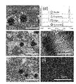
- FIG. 2 shows an SEM image (FIG. 2 (a)) of nuclei formed after the first step (1050 ° C. for 5 minutes) and an SEM image of graphene grown after the second step (6 minutes at 400 ° C.).
- FIG. 2B SEM image (FIG. 2C) of graphene grown after the second step (7 minutes at 400 ° C.), sapphire substrate, production nucleus, graphene, and ⁇ from the graphene edge Raman scattering spectrum (FIG. 2 (d)), AFM image (FIG. 2 (e)) showing that the production nucleus shown in FIG. 2 (a) has a hexagonal spiral structure, and the second It is an AFM image (FIG.2 (f)) which shows the surface state of the graphene obtained after the process.
- the black contrast portion appearing in the SEM image shown in FIG. 2A is a production nucleus formed in the first step.
- Each of the generated nuclei has a substantially hexagonal outline with a diameter of about 2 to 3 ⁇ m, and has a weak contrast region around it. Such generated nuclei are formed at intervals of several ⁇ m.
- graphene grows around the individual nuclei and combines with the graphene grown from the adjacent nuclei to form a single film. You can see how it becomes. Then, as shown in FIG. 2C, it can be confirmed that graphene covers most of the substrate surface 7 minutes after the start of the second step.
- the four ⁇ -Raman scattering spectra shown in FIG. 2D are measured points (sapphire substrate portions) indicated by rhombus marks in FIG. 2A, and square marks (graphene end portions) in FIG. 2B. , Obtained from the measurement points indicated by the triangular mark (graphene part) and the round mark (generated nucleus part).
- the 2D / G ratio of two layers of graphene is about 1, and the 2D / G ratio of four layers of graphene is about 0.5. Therefore, if the 2D / G ratio is 2 or more, it may be determined that the layer is almost complete.
- the present inventors judge the height of “single layer property” by this 2D / G ratio, and evaluate a graphene having a 2D / G ratio of 1 or more as graphene having a high single layer property.
- the product nuclei formed in the first step may already be graphene with extremely high monolayer properties. High nature. And since the 2D / G ratio of the Raman scattering spectrum from the graphene grown in the second configuration also maintains a value close to 2, the above-mentioned graphene having a very single layer property is used as a production nucleus, and a single layer is formed around this. It is thought that graphene with extremely high properties is growing.
- the intensity of the D band due to the defect structure is very low, and the G / D ratio exceeds 10. Accordingly, it is considered that graphene having high crystallinity has already been formed at the stage of formation nuclei, and that graphene is growing around the formation nuclei having high crystallinity while maintaining the crystallinity.
- the area of the graphene obtained depends on the area of the formation region of the product nucleus on the substrate, a large-area high-quality single-layer graphene can be obtained by widening the area.
- nuclei have a hexagonal spiral structure as shown in the AFM image shown in FIG.
- a carbon six-membered ring grows two-dimensionally around this product nucleus and merges with the carbon six-membered ring grown around the adjacent product nucleus to form a graphene film.
- the white linear contrast observed in the AFM image shown in FIG. 2 (f) is a trace that the carbon six-membered rings that have grown from adjacent product nuclei merged into one graphene film.
- this nuclei can be a single-layer graphene or a multilayer graphene. It can also be a production nucleus.
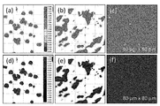
- FIG. 3 shows 2D / G ratio Raman mapping (FIGS. 3 (a) to (c)) and G / D ratio corresponding to each sample whose SEM images are shown in FIGS. 2 (a) to 2 (c). It is a Raman mapping (FIGS. 3D to 3F).
- 3A to 3C are regions that show a 2D / G ratio of 1.5 or more.
- 3 (d) to 3 (f) is a region showing a G / D ratio of 1.5 or more.
- graphene grows two-dimensionally around the production nucleus and eventually becomes a single graphene film.
- the graphene thus obtained is composed of a plurality of domains composed of a set of carbon six-membered rings, and each of the plurality of domains has a carbon six-membered ring nucleus in the domain.
- the orientation of the carbon six-membered ring in the domain is substantially the same over the entire surface of the graphene film, and is substantially the same in a range of at least 10 ⁇ 7 cm 2 .
- substantially the same means that the deviation of the orientation of the carbon six-membered ring in the region of interest is 15 ° or less.
- the density of the production nuclei of the carbon six-membered ring is preferably 1 ⁇ 10 6 pieces / cm 2 or less. If the density of the nuclei is too high, it will be difficult to make the orientation of the carbon six-membered ring in the domain substantially the same over the entire surface of the graphene film.
- the area of one continuous graphene film depends on the area of the formation nucleus formation region on the substrate and is, for example, 1 ⁇ 10 ⁇ 7 cm 2 or more (generally corresponding to 3 ⁇ m ⁇ 3 ⁇ m). In particular, it may be a single layer continuous film.
- FIG. 4 is a TEM image obtained from graphene after completion of the second step. This graphene is grown by setting the CVD reaction temperature in the second step to 500 ° C., but a similar TEM image can be obtained from graphene grown at a temperature of 400 ° C. or lower.
- FIGS. 4 (a) is a dark field image
- FIG. 4 (b) is a bright field image
- FIGS. 4 (c) and 4 (d) are high magnification images.
- the difference in the orientation of the carbon six-membered ring in the film was less than 5%. That is, it can be confirmed that the single-layer graphene obtained by the present invention is composed of an assembly of carbon six-membered rings whose orientations are substantially aligned in the same direction over the entire surface of the film.
- the generated nuclei in the first step are not required to be formed by the CVD method as described above, and may be performed, for example, by transferring graphite or graphene to the main surface of the substrate by a peeling method.
- the first step may be performed by patterning graphite or graphene on the main surface of the substrate by a photolithographic method.
- a step of separating graphene from the substrate may be provided following the second step.
- Graphene has a unique conical band structure with a smooth side surface in which the conduction band and the valence band are in contact at one point (Dirac point). Since it has such a specific band structure, electrons in graphene are in a kind of free state, and the mobility of carriers shows a very large value. Taking advantage of this characteristic, carrier density (conductivity) can be continuously controlled by providing graphene in the gate region and changing the voltage applied to the graphene.
- graphene is applied to electronic devices, its good conductivity, high electron / hole mobility, inelastic electron conductivity and spin conductivity, mechanical strength, light absorption and emission, heat conduction, etc. High performance electronic devices can be realized due to superior characteristics.
- an electronic element for example, a field effect transistor having a channel region made of such graphene can be exemplified.
- the electronic device is, for example, a metal having a catalytic action for graphene synthesis and having a melting point of 400 ° C. or lower (for example, at least one of gallium and indium, or gallium- Indium alloy) is brought into contact, a gas containing hydrocarbon is supplied in a state where the metal is maintained at a temperature exceeding the melting point, graphene is grown at the contact interface with the metal on the substrate main surface, and the resist pattern is graphene It can be manufactured by a process including a step of forming a circuit by forming a circuit.
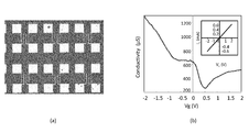
- FIG. 5 is an example of an optical micrograph (FIG. 5 (a)) of an FET experimentally produced by the present inventors using the graphene described above, and its CV curve (FIG. 5 (b)).
- the hole mobility is estimated at about 600 cm 2 / V s .
- a sapphire substrate (1 cm ⁇ 1 cm) having an off angle of 0.2 ° was used as the substrate.
- a cleaning process by oxygen plasma ashing is performed, gallium metal is placed on the main surface of the sapphire substrate, and as shown in FIG. Inserted into.
- RF heating was performed while flowing Ar gas as a carrier gas to raise the substrate temperature to 850 ° C., and this temperature was maintained to melt gallium.
- RF heating is performed while flowing Ar gas as a carrier gas to raise the substrate temperature to 200 ° C.
- Ar gas is flowed at 200 sccm and CH 4 gas at a flow rate (0.5 atm), and the substrate temperature is 200 ° C. Hold at 10 ° C. for 10 minutes. Thereafter, the supply of CH 4 gas was stopped and cooled to room temperature in an Ar gas atmosphere.
- FIG. 6 is an SEM image of graphene thus obtained.
- the obtained graphene is composed of a plurality of domains composed of a set of carbon six-membered rings, and each of the plurality of domains has a generation nucleus of the carbon six-membered ring in the domain. Are connected neatly to form a single film.
- a sapphire substrate (1 cm ⁇ 1 cm) having an off angle of 0.2 ° was used as the substrate.
- a cleaning process by oxygen plasma ashing is performed, gallium metal is placed on the main surface of the sapphire substrate, and as shown in FIG. Inserted into.
- RF heating was performed while flowing Ar gas as a carrier gas to raise the substrate temperature to 850 ° C., and this temperature was maintained to melt gallium.
- RF heating is performed while flowing Ar gas as a carrier gas to raise the substrate temperature to 200 ° C.
- Ar gas is flowed at 200 sccm and CH 4 gas at a flow rate (0.5 atm), and the substrate temperature is 200 ° C. Hold at 20 ° C. for 20 minutes. Thereafter, the supply of CH 4 gas was stopped and cooled to room temperature in an Ar gas atmosphere.
- a sapphire substrate (1 cm ⁇ 1 cm) having an off angle of 0.2 ° was used as the substrate.
- a cleaning process by oxygen plasma ashing is performed, gallium metal is placed on the main surface of the sapphire substrate, and as shown in FIG. Inserted into.
- RF heating was performed while flowing Ar gas as a carrier gas to raise the substrate temperature to 850 ° C., and this temperature was maintained to melt gallium.
- RF heating is performed while flowing Ar gas as a carrier gas to raise the substrate temperature to 100 ° C.
- Ar gas is flowed at 200 sccm and CH 4 gas at a flow rate (0.5 atm), and the substrate temperature is set to 100 ° C. Hold at 60 ° C. for 60 minutes. Thereafter, the supply of CH 4 gas was stopped and cooled to room temperature in an Ar gas atmosphere.
Landscapes
- Chemical & Material Sciences (AREA)
- Organic Chemistry (AREA)
- Inorganic Chemistry (AREA)
- Carbon And Carbon Compounds (AREA)
- Thin Film Transistor (AREA)
Abstract
本発明では、第1の工程において、基板の主面に炭素六員環の生成核を形成し、これに続き、第2の工程において、生成核を形成した基板の主面に、グラフェン合成の触媒作用を有する金属であって融点が400℃以下のガリウム等の金属を接触させ、該金属を融点を超える温度に保持した状態で炭化水素を含有するガスを供給し、前記基板主面の金属との接触界面にグラフェンを成長させる。原料ガスは、100℃程度の極めて低い温度でも、上記液体金属の表面で水素と炭素に分解し、液体金属の表面にあるガリウム等の原子と結合する。炭素原子は、このガリウム等の原子に導かれるかたちで液体金属の表面を容易に拡散し、基板主面との接触界面への炭素の供給が速やかになされる。
Description
本発明はグラフェンの製造技術に関し、より詳細には、大面積かつ高品質の単層グラフェンを低温で製造する技術ならびに斯かるグラフェンを電子素子に応用する技術に関する。
グラフェンは、その理想的な2次元構造に起因して様々な特異的性質を有しており、例えば、良伝導性、高い電子・正孔移動度を有している。これに加えて、非弾性的な電子伝導性やスピン伝導性、力学的強度、光吸収および発光、熱伝導等の特性も注目されており、各種分野への工業的応用が期待されている物質である。
グラフェンの製造方法としては、現在、熱分解黒鉛結晶からの剥離方法、固相反応法、化学気相成長法等が知られている。
グラフェンの最初の発見はNovoselov等によるものであり、このグラフェンは、熱分解黒鉛結晶をスコッチテープで剥離し、Si基板へ転写させたものである。グラフェン結晶のサイズは数ミクロン程度のものであるが、比較的再現性良く容易にグラフェン膜が得られることが特徴である(非特許文献1、2)。
固相反応法では、炭化ケイ素結晶を2000℃度程度で真空熱処理することで表面のSi元素を蒸発(シリコンサブリメーション)させ、炭化ケイ素表面にグラフェン結晶層を形成する(非特許文献3~7)。
気相成長法では、ニッケルや鉄等の金属結晶表面に炭化水素ガスを原料として熱CVD法により成長させることでグラフェン膜を形成する(非特許文献8、9)。
また、銅箔を触媒とするプラズマCVD法によれば、300~400℃の低い基板温度でグラフェンの合成が可能とされるが(非特許文献10)、得られるグラフェンは単層ではなく多層である。
さらに、プラズマアシスト法によれば、600℃程度の比較的低い基板温度でも単層のグラフェンが得られるとされるが(非特許文献11)、得られたグラフェンのラマン散乱スペクトルには、1300cm-1近傍に現れる欠陥起因の非常に強いDピークが観察される。加えて、基板温度の低温化に伴い微小なグラフェン核が多量に生成し、その結果、合成されたグラフェン膜をミクロに見ると粒界が高密度で存在し、これが電子移動度を顕著に低下させてしまう。また、プラズマイオンによる衝撃により膜の表面や内部に欠陥が形成され、電気特性を劣化させるという問題もある。
このように、従来の方法では、単層のグラフェンを比較的低温で得ることは非常に困難であり、例えば熱CVDによる気相成長法では数十層が積層したグラファイト膜に近いものとなっている。
しかも、合成されたグラフェンを母材から単離し、Si等の電子素子基板上に転写等することも非常に困難であるため、電子素子への応用という観点からの問題もある。
電子デバイスやセンサ、配線等の部品の一部としてグラフェンを利用する場合、所望の位置に所望の方向でグラフェンを配置することが重要な技術的課題となるが、上記した従来の方法ではこのような技術的課題に有効に対処できないという問題点がある。
これらの問題点の主要因は、既存のグラフェン素子報告例にあるように熱分解黒鉛結晶をスコッチテープで剥離し、偶然に再転写されたグラフェン膜を見つけ出して素子形成に利用されているという事実が示すように、大面積のグラフェン膜を得ることが非常に困難であるという事情に由来する。剥離されたグラフェン自体のサイズや均一性には大きなばらつきがあり、その転写位置を任意に制御できないこと等も大きな要因である。さらにグラフェンは本来、炭素六員環で構成される1原子層の究極的な厚さの膜であるため、大面積での取り扱いには根本的・原理的な困難が伴う。
加えて、グラフェンの特長を生かした電子素子等への応用の観点からは、大面積かつ高品位の単層のグラフェンの合成温度の更なる低温化を可能とする技術が望まれる。
低温でのグラフェンの合成という課題につき、本発明者らは、大面積のグラフェンを、高温を必要とすることなく製造することができるグラフェン膜の製造方法を提案した(特許文献1)。
特許文献1において本発明者らが報告した手法では、まず目的のグラフェン膜の原料として、例えば直径数ミリから数センチの径を有し、厚さが数ナノメートルのアモルファスカーボン膜を合成する。
具体的には、アモルファスカーボン膜の原料として、コロジオン膜やフォルンバール膜等の有機膜を形成し、この有機膜をアルミナ等のセラミックスリングですくい取り、セラミックスリングの上に有機膜を張る。
次いで、この有機膜を真空熱処理することによりアモルファス状に炭化させてアモルファスカーボン膜を合成する。例えば、有機膜を張ったセラミックスリングを500℃で30分真空熱処理すると有機膜が分解し、炭素に変性する。
さらに、このようにして得られたアモルファスカーボン膜を液体ガリウムの表面に接触させて転写し、真空中で熱処理を行う。液体ガリウムの非常に強い表面張力のために液面は凸状に盛り上がり、この液体ガリウムの凸状液面にアモルファスカーボン膜が転写される。
そして、このアモルファスカーボン膜を、例えば、真空中1000℃で10~30分程度熱処理を行うことで、液体ガリウムとアモルファスカーボン膜との接触界面にグラフェンが形成される。
Novoselov, K. S. et al. "Electric field effect in atomically thin carbon films" Science 306 (2004) 666-669.
Meyer JC, et al, "The structure of suspended graphene sheets" Nature. 446(7131) (2007) 60-63.
A. J. van Bommel, et al. "A. LEED and Auger electron observations of the SiC(0001) surface" Surf. Sci. 48 (1975) 463-472.
I. Forbeaux et al. "Heteroepitaxial graphite on 6H-SiC(0001): Interface formation through conduction-band electronic structure" Phys. Rev. B 58 (1998) 16396-16406.
Berger, C. et al. "Ultrathin epitaxial graphite: 2D electron gas properties and a route toward graphene-based nanoelectronics" J. Phys. Chem. B, 108, (2004) 19912-19916.
Berger, C. et al. "Electronic confinement and coherence in patterned epitaxial grapheme", Science 312, (2006) 1191-1196.
Ohta, T. et al. "Controlling the electronic structure of bilayer grapheme",Science 313 (2006) 951 - 954.
T. A. Land, et al. "STM investigation of single layer graphite structures produced on Pt(111) by hydrocarbon decomposition", Sur. Sci. 264 (1992) 261-270.
A. Nagashima et al. "Electronic states of monolayer graphite formed on TiC(111) surface", Surf. Sci. 291 (1993) 93-98.
J. Kim et al. "Low-temperature synthesis of large-area graphite-based transparent conductive films using surface wave plasma chemical vapor deposition" Appl. Phys. Lett., 98, 091502 (2011).
S. Chan et al. "Low-temperature synthesis of graphite on Cu using plasma-assisted thermal chemical vapor deposition" Nanoscale Res. Lett., 8, 285 (2013).
特許文献1の手法は低温でのグラフェンの合成を課題とするものであるが、本発明者らの、「ガリウムと炭素との反応過程の研究から液体ガリウムとアモルファス炭素との界面でグラファイト化反応が約1000℃程度の比較的低温で誘起され、大面積のグラフェンの形成が可能である」との知見に基づくものであるため、その低温化は充分とは言えない。
上述のとおり、グラフェンの特長を生かした電子素子等への応用の観点からは、大面積かつ高品質の単層グラフェンの低温合成技術が望まれるところであり、特に、既存のシリコンデバイスとのハイブリッド化を想定した場合には、400℃程度での低温でも上記グラフェンを製造可能とする技術が望まれる。
本発明は、このような従来法の抱える問題に鑑みてなされたもので、その目的とするところは、大面積かつ高品位のグラフェンを、従来法では到底成し得なかったほどの低温で製造する技術を提供することにある。
上記課題に鑑みてなされた本発明に係る第1の態様のグラフェンの製造方法は、基板の主面に炭素六員環の生成核を形成する第1の工程と、前記生成核の周りで2次元的に炭素六員環を形成してグラフェン膜とする第2の工程を備え、前記第2の工程における炭素六員環の形成を300℃以下の温度で実行する、ことを特徴とする。
ある態様では、前記第1の工程において、前記基板の主面に融点が400℃以下の金属の液滴を接触させた状態で炭化水素を含有するガスを供給し、前記基板の主面と前記金属との接触面に前記生成核を形成する。
例えば、前記融点が400℃以下の金属は、ガリウム、インジウム、ガリウム-インジウム合金の群から選択される少なくとも1種である。
また、他の態様では、前記第1の工程における生成核の形成を、フォトリソグラフィ法により予め前記基板の主面に配列されたアモルファス炭素の核を形成しておき、該基板の主面に液体ガリウムを接触させた状態で熱処理して実行する。
さらに、他の態様では、前記第1の工程で形成される生成核は、剥離法により形成された炭素六員環である。
好ましくは、前記第2の工程において、前記生成核が形成された基板の主面領域にグラフェン合成の触媒作用を有する金属であって融点が400℃以下の金属を接触させた状態で炭化水素を含有するガスを供給し、前記基板の主面と前記金属との接触界面から前記炭素六員環を形成させてグラフェン膜とする。
また、好ましくは、前記触媒作用を有する金属として前記炭素六員環の形成温度よりも低い融点を有する金属を選択し、該金属の液滴を前記基板の主面領域に接触させた状態で前記炭素六員環を形成させる。
例えば、前記融点が400℃以下の金属は、ガリウム、インジウム、ガリウム-インジウム合金の群から選択される少なくとも1種である。
好ましくは、前記炭化水素を含有するガスをプラズマ化して供給する。
本発明に係る第2の態様のグラフェンの製造方法は、基板の主面に炭素六員環の生成核を形成する第1の工程と、前記生成核を形成した基板の主面に、グラフェン合成の触媒作用を有する金属であって融点が400℃以下の金属を接触させ、該金属を融点を超える温度に保持した状態で炭化水素を含有するガスを供給し、前記基板主面の金属との接触界面にグラフェンを成長させる第2の工程と、を備えている。
例えば、前記融点が400℃以下の金属は、ガリウム、インジウム、ガリウム-インジウム合金の群から選択される少なくとも1種である。
好ましくは、前記第1の工程は、前記基板を1000℃以上の温度に保持した状態で炭化水素を含有するガスを供給して実行される。
また、好ましくは、前記第1の工程は、前記基板の主面に、グラフェン合成の触媒作用を有する金属であって融点が1000℃未満の金属を接触させた状態で前記炭化水素を含有するガスを供給して実行される。
例えば、前記融点が1000℃未満の金属は、ガリウム、インジウム、アンチモンおよびそれらの合金の群から選択される少なくとも1種である。
ある態様では、前記第1の工程は、剥離法により前記基板の主面にグラファイト若しくはグラフェンを転写して実行される。
また、他の態様では、前記第1の工程は、フォトリソグラフ法により前記基板の主面にグラファイト若しくはグラフェンをパターニングして実行される。
さらに、他の態様では、前記第2の工程は、プラズマアシスト法により前記炭化水素ガスの分解効率を高めて実行される。
好ましくは、前記第2の工程は、融点が400℃以下の金属としてガリウムを選択し、300℃以下の温度で実行される。
また、好ましくは、前記第2の工程に続き、前記基板から前記グラフェンを分離する第3の工程を備えている。
例えば、前記基板はオフ角の絶対値が30°以内の(0001)面(C面)を主面とするサファイヤである。
本発明に係る電子素子の製造方法は、基板主面に形成されたレジストパターンに、グラフェン合成の触媒作用を有する金属であって融点が400℃以下の金属を接触させ、該金属を融点を超える温度に保持した状態で炭化水素を含有するガスを供給し、前記基板主面の金属との接触界面にグラフェンを成長させ、前記レジストパターンをグラフェン化して回路を形成する工程を含むことを特徴とする。
例えば、前記融点が400℃以下の金属は、ガリウム、インジウム、およびそれらの合金の群から選択される少なくとも1種である。
本発明に係るグラフェンは、炭素六員環の集合からなる複数のドメインから構成され、前記複数のドメインのそれぞれは、該ドメイン内に前記炭素六員環の生成核を有し、その密度が1×106cm-2以下であることを特徴とする。
好ましくは、前記ドメイン内の炭素六員環の方位がグラフェン膜の少なくとも10-7cm2の範囲内で実質的に同一であり、1×10⁻⁷cm2以上の面積を有する連続膜であり、実質的に単層の膜である。
また、好ましくは、前記グラフェンから得られるラマン散乱スペクトル中に認められる2700cm-1近傍の2Dバンドのピークと1590cm-1近傍のGバンドのピークの強度比(2D/G比=I2D/IG)が1以上である。
さらに、好ましくは、前記グラフェンから得られるラマン散乱スペクトル中に認められる1590cm-1近傍のGバンドのピークと1300cm-1近傍のDバンドのピークの強度比(G/D比=IG/ID)が3以上である。
本発明に係る電子素子は、上述のグラフェンを備えた電子素子である。
好ましい態様では、前記グラフェンから成るチャネル領域を有する。
本発明では、基板上に予め炭素六員環の生成核を形成し、この生成核の周りで、2次元的な炭素六員環の形成を行うこととした。これにより、大面積かつ高品質の単層グラフェンの低温合成技術が提供される。
このようなグラフェンを電子素子に応用することにより、その良伝導性、高い電子・正孔移動度、非弾性的な電子伝導性やスピン伝導性、力学的強度、光吸収および発光、熱伝導等の優位な特性により、高性能の電子素子を実現できる。
以下に、図面を参照して、本発明に係るグラフェンおよびその製造方法ならびに電子素子への応用例につき、説明する。
本発明は、ガリウム等の金属を触媒として用い、メタン等の炭化水素ガスを炭素源としてグラフェンを合成させることとすると、予め炭素六員環の生成核を形成させておいた基板上には、従来の手法でグラフェンを合成する温度よりも遥かに低い100℃程度の極めて低い温度でも、実質的に単層のグラフェンが大面積かつ高品質で得られるという、本発明者らの新たな知見に基づくものである。
上述の特許文献1にも記載があるように、冶金学的にみれば、ガリウムと炭素とは全律非固溶である。しかし、X線吸収端スペクトル(NEXAFS)のデータから、ガリウム原子と炭素原子との結合が形成されることが示されている。本発明者らは更に検討を進めた結果、基板上に予め炭素六員環の生成核を形成させておけば、この生成核の周りで、2次元的な炭素六員環の形成が、100℃程度の極めて低い温度でも進行するという知見を得るに至った。
なお、以下の説明では、触媒として作用する金属をガリウムとして説明するが、本発明は、ガリウムと同様の触媒作用を有する金属を排除するものではなく、斯かる金属としては、例えば、インジウムおよびアンチモンを例示することができる。また、このような触媒作用を有するものとして、ガリウム、インジウム、アンチモンの合金を用いてもよい。
図1は、本発明に係るグラフェンを合成(製造)するための手法の一例を説明するための図で、図1(a)は反応系の構成例を示す図であり、図1(b)はプロセス温度シーケンスの例を示す図である。
この図に示した反応系の例では、第1の工程として、高周波加熱が可能な石英管100の内部に、基板10の主面に、グラフェン合成の触媒作用を有する金属であって融点が1000℃未満の金属20を接触させた状態で、炭化水素を含有するガスを供給して、CVD法により基板10の主面に炭素六員環の生成核を形成する。
炭素六員環の生成核は、例えば6角形状のグラファイトや多層のグラフェンであり、そのような生成核の源となる炭素は基板10と金属20との接触界面に供給され、当該界面領域に生成核が形成されることになる。
上記金属20の融点を1000℃未満とするのは、グラフェン合成の触媒作用を奏するためには金属20が液体の状態にある必要があること、そして、炭素六員環の生成核を効率的に形成するためには1000℃以上の温度が必要となることによる。
つまり、図1(a)に示した例では、第1の工程において、基板10を1000℃以上の温度に保持した状態で炭化水素を含有するガスを供給することにより、CVD法により生成核の形成が実行される。
ここで、上述の融点が1000℃未満の金属は、ガリウム(融点29.78℃)はもとより、インジウム(融点156.61℃)、アンチモン(融点630.74℃)などを例示することができ、これらの金属のうちの少なくとも1種が選択される。また、これらの金属に代えて、ガリウム、インジウム、アンチモンの合金を用いてもよい。つまり、上述した「融点が1000℃未満の金属」として、ガリウム、インジウム、アンチモンおよびそれらの合金の群から選択される少なくとも1種を選択するようにして良い。
後述のとおり、本発明の方法によれば、300℃以下といった低温でのグラフェンの成膜も可能となるが、その前提となるのが、基板の主面への炭素六員環の生成核の形成である。
図1に示した例では、基板の主面に炭素六員環の生成核を形成するに際し、基板の主面にラフェン合成の触媒作用を有する金属であって融点が1000℃未満の金属を接触させた状態で、炭化水素を含有するガスを供給している。しかし、このような方法の他に、以下のようにして、基板の主面に炭素六員環の生成核を形成してもよい。
例えば、基板の主面に融点が400℃以下の金属の液滴を接触させた状態で炭化水素を含有するガスを供給し、基板の主面と金属との接触面に炭素六員環の生成核を形成することもできる。
この場合、融点が400℃以下の金属としては、ガリウム、インジウム、ガリウム-インジウム合金の群から選択される少なくとも1種を例示することができる。
また、フォトリソグラフィ法により予め基板の主面に配列されたアモルファス炭素の核を形成しておき、該基板の主面に液体ガリウムを接触させた状態で熱処理することで、基板の主面と金属との接触面に炭素六員環の生成核を形成することもできる。
さらに、剥離法により基板の主面に炭素六員環を形成して、これを生成核としてもよい。
このような生成核を予め設けておくことにより、後述のグラフェンの成長工程において、当該生成核の周りで2次元的に炭素六員環が形成されてグラフェン膜となる。
この第1の工程に続く第2の工程では、生成核形成後の基板10の主面に、例えば、グラフェン合成の触媒作用を有する金属であって融点が400℃以下の金属25を接触させた状態で、第1の工程と同様に炭化水素を含有するガスを供給してグラフェンを成長させる。
つまり、第2の工程において、生成核が形成された基板の主面領域にグラフェン合成の触媒作用を有する金属であって融点が400℃以下の金属を接触させた状態で炭化水素を含有するガスを供給し、基板の主面と金属との接触界面から前記炭素六員環を形成させてグラフェン膜とする。
例えば、触媒作用を有する金属として炭素六員環の形成温度よりも低い融点を有する金属を選択し、該金属の液滴を基板の主面領域に接触させた状態で炭素六員環を形成させる。
例えば、前記融点が400℃以下の金属は、ガリウム、インジウム、ガリウム-インジウム合金の群から選択される少なくとも1種である。
また、炭化水素を含有するガスを供給してグラフェンを成長させる際に、当該炭化水素を含有するガスをプラズマ化して供給するようにしてもよい。
グラフェンを構成することとなる炭素原子は、基板10と金属25との接触界面に供給され、当該界面領域にある生成核の周りにグラフェンがCVD成長することになる。
上記金属25の融点を400℃以下とするのは、グラフェン合成の触媒作用を奏するためには金属25が液体の状態にある必要があること、そして、本発明ではグラフェン合成温度の低温化を目的としており、特に、既存のシリコンデバイスとのハイブリッド化を想定して400℃程度での低温でのグラフェンの合成を目的としていることによる。勿論、第2の工程の処理温度を400℃を超える温度としても、本発明に係るグラフェンの製造が可能であることは言うまでもない。
ここで、上述のとおり、融点が400℃以下の金属は、ガリウム(融点29.78℃)やインジウム(融点156.61℃)を例示することができ、これらの合金であってもよい。
このように、本発明のグラフェンの製造方法の第1の態様は、基板の主面に炭素六員環の生成核を形成する第1の工程と、前記生成核の周りで2次元的に炭素六員環を形成してグラフェン膜とする第2の工程を備え、前記第2の工程における炭素六員環の形成を300℃以下の温度で実行する。この場合、好ましくは、前記第1の工程において、前記基板の主面に融点が400℃以下の金属の液滴を接触させた状態で炭化水素を含有するガスを供給し、前記基板の主面と前記金属との接触面に前記生成核を形成する。
また、本発明のグラフェンの製造方法の第2の態様は、基板の主面に炭素六員環の生成核を形成する第1の工程と、前記生成核を形成した基板の主面に、グラフェン合成の触媒作用を有する金属であって融点が400℃以下の金属を接触させ、該金属を融点を超える温度に保持した状態で炭化水素を含有するガスを供給し、前記基板主面の金属との接触界面にグラフェンを成長させる第2の工程と、を備えている。
炭素源となる炭化水素ガス種の選定を含め、CVD条件は適宜最適化されるが、例えば、石英管100内に、ソースガスとして、5%のメタン(CH4)ガスを1sccmと純度6Nのアルゴン(Ar)ガスを250sccm供給し、CVD反応中の圧力を概ね0.5気圧に維持する。この条件では、メタンの分圧は概ね10Paとなる。
基板10としては、例えば、オフ角の絶対値が30°以内の(0001)面(C面)を主面とするサファイヤを用いることができる。これは、C面内での原子配列が6回対称性を有しているため、炭素六員環の原子配列の対称性と一致するという利点が期待できるためである。また、オフ角は生成核形成の際のキンクとなるステップの密度(およびテラス幅)を考慮して、適宜選択すればよい。なお、グラフェンの成長のためには、ベンゼン環が2個繋がることのできるテラス幅は必要であると考えられるため、オフ角の絶対値は30°以内であることが好ましい。本発明者らは、主として、オフ角の絶対値が0.2°のC面サファイヤ基板を用いた。
触媒として作用する金属20(25)としての液体ガリウムは、サファイヤの基板10の主面との濡れ性が低い。そのため、液体ガリウムは基板上に「液滴状で乗っている」状態に近く、基板主面との接触界面もまた、「表面」としての性質を維持している。その結果、接触角は90°を超えて大きく盛り上がった状態で基板主面に接触している。
石英管100内に原料ガスが供給されると、例えば100℃程度の極めて低い温度でも、液体ガリウムの表面でメタンガスが水素(HまたはH2)と炭素(C)に分解する。上述のとおり、ガリウムと炭素とは全律非固溶であるものの、ガリウム原子と炭素原子との結合が起こり得るため、メタンガスの分解により生じた炭素原子の一部が液体ガリウムの表面にあるガリウム原子と結合する。
そしてガリウムは液体状態にあるため、表面(基板主面との接触界面も含む)近傍での原子の拡散が容易に生じる。従って、表面にあるガリウム原子と結合した炭素原子は、このガリウム原子に導かれるかたちで液体ガリウムの表面を容易に拡散し、基板主面との接触界面への炭素の供給が速やかになされる。一方、液体ガリウムの「液滴」内部には炭素原子は殆ど供給されないから、基板主面との接触界面への炭素原子の供給は液体ガリウムの表面(基板主面との接触界面も含む)からのみなされることとなる。つまり、本発明の手法では、基板主面への炭素原子の供給は、実質的に2次元的なものに限られ、3次元的な炭素原子の供給が抑制されるため、単層のグラフェンの合成に極めて有利である。
図1(b)に示したシーケンス例では、Ar雰囲気中で1050℃まで昇温し、メタンガスを供給して第1の工程(1st step)を実行している。この第1の工程における生成核形成はメタンガス供給直後から始まり、5分程度の短時間で充分な密度の生成核が形成される。本発明者らが、ガリウムを触媒金属として、オフ角が0.2°のC面サファイヤ基板(1cm2)の基板上への生成核形成実験を行った例では、1050℃の温度で5分間の反応後、6角形のスパイラル構造を有する生成核が105cm-2オーダーの密度で得られていた。
図1(b)に示した例では、上述の第1の工程後、メタンガスの供給を停止して石英管100内で基板10を急冷し、再度、400℃まで昇温し、メタンガスを供給して第2の工程(2nd step)を実行し、第1の工程で形成させたグラフェンの生成核を中心として、炭素六員環を成長させる。
なお、400℃よりも低い温度(例えば100℃)でもグラフェンは成長し、特に、融点が400℃以下の金属としてガリウムを選択した場合には、300℃以下の温度でも、高品質な単層のグラフェンを第面積で得ることができる。但し、温度の低下に伴い、炭素原子が液体ガリウムの表面を拡散する速度は低下し、その結果、生成核への供給速度が低下するから、所定の面積の単層グラフェンを得るための反応時間は長くなる。つまり、第2の工程の反応時間は、反応温度と、最終的に得たいグラフェンの膜面積に応じて、適宜設定されることとなる。
なお、グラフェンの成長温度を低くしたために成長速度が低下する問題に対しては、プラズマアシスト法により炭化水素ガスの分解効率を高める手法が効果的である。プラズマアシスト法を応用すれば、成長温度を低くした場合でも、所望の成長速度を確保し得る。
図2は、第1の工程(1050℃で5分)後に形成された生成核のSEM像(図2(a))、第2の工程(400℃で6分)後に成長したグラフェンのSEM像(図2(b))、同じく第2の工程(400℃で7分)後に成長したグラフェンのSEM像(図2(c))、サファイヤ基板、生成核、グラフェン、およびグラフェン端部からのμラマン散乱スペクトル(図2(d))、図2(a)に示した生成核が6角形のスパイラル構造を有している様子を示すAFM像(図2(e))、そして、第2の工程後に得られたグラフェンの表面状態を示すAFM像(図2(f))である。
図2(a)に示したSEM像に表れている黒いコントラスト部分が、第1の工程で形成された生成核である。この生成核のそれぞれは、直径が2~3μm程度の略6角形の輪郭を呈しており、その周りに、弱いコントラストの領域を有している。そして、このような生成核が、数μm間隔で形成されている。
図2(b)をみると、第2の工程を開始した6分後には、個々の生成核の周りにグラフェンが成長し、隣接した生成核から成長してきたグラフェンと結合してひとつの膜になってゆく様子が確認できる。そして、図2(c)に示されているように、第2の工程を開始した7分後には、基板表面のほとんどをグラフェンが覆っている様子を確認することができる。
図2(d)に示した4つのμラマン散乱スペクトルは、図2(a)中に菱形マークで示した測定ポイント(サファイヤ基板部)、図2(b)中に四角マーク(グラフェン端部)、三角マーク(グラフェン部)、丸マーク(生成核部)で示した測定ポイントから得られたものである。
これらのスペクトル中に認められる1550cm-1近傍のピークと2320cm-1近傍のピークは何れも、サファイヤ基板に起因のものである。
生成核から得られたラマン散乱スペクトルをみると、2700cm-1近傍の2Dバンドのピークと1590cm-1近傍のGバンドのピークが明瞭に認められる。また、1300cm-1近傍のDバンドの弱いピークも認められる。
単層カーボンナノチューブの発見当初から、炭素素材のラマン散乱スペクトルについては多くの研究報告がなされてきた。グラフェンから得られるラマン散乱スペクトルには、格子振動に由来する特徴的なピークが現れ、上記Gバンドはグラファイトにおける炭素原子の6員環構造の面内伸縮振動に起因するバンドである。また、上記Dバンドはその欠陥構造による非弾性散乱を伴う二重共鳴効果によって現れるピークであることが知られており、これらのバンドの強度比(G/D比=IG/ID)は、グラフェンの結晶性の高さの指標となる。本発明者らは、「結晶性」の高さをこのG/D比で判定することとし、G/D比が3以上のものを、結晶性の高いグラフェンと評価している。
また、上記2Dバンドはグラフェンシート層間における相互作用の影響を受けるため、Gバンドとの強度比(2D/G比=I2D/IG)はグラフェンの層数(単層性)の評価の指標となる。例えば、2層のグラフェンの2D/G比は1程度であり、4層のグラフェンの2D/G比は0.5程度である。従って、2D/G比が2以上あれば、ほぼ完全な単層と判断してよい。本発明者らは、「単層性」の高さをこの2D/G比で判定することとし、2D/G比が1以上のものを、単層性の高いグラフェンと評価している。
生成核から得られたラマン散乱スペクトルの2D/G比は2に近い値を示しているから、第1の工程で形成される生成核は既に、単層性の極めて高いグラフェンとなっている可能性が高い。そして、第2の構成で成長したグラフェンからのラマン散乱スペクトルの2D/G比も2に近い値を維持しているから、上記単層性の極めて高いグラフェンを生成核として、この周りに単層性の極めて高いグラフェンが成長しているものと考えられる。
また、生成核とグラフェンの何れのスペクトルにおいても、欠陥構造に起因するDバンドの強度は非常に低く、G/D比は10を超えている。従って、生成核の段階で既に結晶性の高いグラフェンが形成されており、この結晶性の高い生成核の周りにその結晶性を維持しつつグラフェンが成長しているものと考えられる。
このように、本発明によれば、2700cm-1近傍の2Dバンドのピークと1590cm-1近傍のGバンドのピークの強度比(2D/G比=I2D/IG)が1以上である単層性の高いグラフェンを、極めて低温で合成することが可能である。
また、本発明によれば、1590cm-1近傍のGバンドのピークと1300cm-1近傍のDバンドのピークの強度比(G/D比=IG/ID)が3以上である高品質なグラフェンを、極めて低温で合成することが可能である。
そして、得られるグラフェンの面積は、基板上の生成核の形成領域の面積に依存するから、当該面積を広くすることで、大面積の高品質な単層グラフェンを得ることができる。
上述の生成核の殆どは、図2(e)に示したAFM像に示されているように、6角形のスパイラル構造を有している。そして、第2の工程において、この生成核の周りに炭素六員環が2次元的に成長し、隣接する生成核の周りに成長してきた炭素六員環と合体し、グラフェンの膜が形成される。図2(f)に示したAFM像中に観察される白い線状のコントラストは、隣接する生成核から成長してきた炭素六員環同士が合体してひとつのグラフェン膜となった痕跡である。
この生成核がどのような炭素生成物となるかは第1の工程の処理温度および時間にも依存するが、単層のグラフェンとすることもできるし多層のグラフェンとすることもでき、グラファイトの生成核とすることもできる。
図3は、図2(a)~(c)にSEM像を示した各試料に対応する、2D/G比のラマン・マッピング(図3(a)~(c))およびG/D比のラマン・マッピング(図3(d)~(f))である。
図3(a)~(c)で濃く示されている領域は、1.5以上の2D/G比を示した領域である。また、図3(d)~(f)で濃く示されている領域は、1.5以上のG/D比を示した領域である。第2の工程において、生成核の周りでグラフェンが2次元的に成長し、やがてひとつのグラフェン膜となる様子が見て取れる。
このようにして得られたグラフェンは、炭素六員環の集合からなる複数のドメインから構成され、複数のドメインのそれぞれは、該ドメイン内に炭素六員環の生成核を有する。
そして、ドメイン内の炭素六員環の方位は、グラフェン膜の全面に渡り実質的に同一であり、少なくとも10-7cm2の範囲内で実質的に同一である。ここで、「実質的に同一」とは、着目する領域内における炭素六員環の方位のズレが15°以下であることを意味している。
炭素六員環の生成核の密度は1×10⁶個/cm2以下であることが好ましい。生成核の密度が高すぎると、ドメイン内の炭素六員環の方位を、グラフェン膜の全面に渡り実質的に同一にすることが難しくなる。
上述のとおり、連続する1枚のグラフェン膜の面積は、基板上の生成核の形成領域の面積に依存し、例えば1×10⁻⁷cm2以上(概ね3μm×3μmに相当する)の、実質的に単層の連続膜とすることもできる。
図4は、第2の工程終了後のグラフェンから得られたTEM像である。なお、このグラフェンは第2の工程のCVD反応温度を500℃に設定して成長させたものであるが、400℃以下の温度で成長させたグラフェンからも同様のTEM像が得られる。
図4(a)は暗視野像、図4(b)は明視野像であり、図4(c)および(d)は高倍率像である。図4(c)および(d)に示した格子像を解析した結果、膜内での炭素六員環の方位の差は5%未満であった。つまり、本発明で得られる単層のグラフェンは、膜の全面に渡り、その方位が実質的に同一方向に揃った炭素六員環の集合からなることが確認できる。
なお、第1の工程での生成核は、上述のようなCVD法による必要はなく、例えば、剥離法により、基板の主面にグラファイト若しくはグラフェンを転写して実行してもよい。
また、第1の工程は、フォトリソグラフ法により、基板の主面にグラファイト若しくはグラフェンをパターニングして実行してもよい。
さらに、第2の工程に続き、基板からグラフェンを分離する工程(第3の工程)を設けるようにしてもよい。
グラフェンは、伝導帯と価電子帯が1点(ディラックポイント)で接している滑らかな側面を有する円錐形状の特異なバンド構造を有している。このような特異的なバンド構造を有するため、グラフェン中の電子は一種の自由状態にあり、キャリアの移動度は極めて大きい値を示す。この特性を生かし、ゲート領域にグラフェンを設けてこのグラフェンに印加する電圧を変化させれば、キャリア密度(伝導度)を連続的に制御することができる。
このようなグラフェンを電子素子に応用すれば、その良伝導性、高い電子・正孔移動度、非弾性的な電子伝導性やスピン伝導性、力学的強度、光吸収および発光、熱伝導等の優位な特性により、高性能の電子素子を実現できる。そのような電子素子としては、例えば、斯かるグラフェンから成るチャネル領域を有する電界効果トランジスタを例示することができる。
上記電子素子は、例えば、基板主面に形成されたレジストパターンに、グラフェン合成の触媒作用を有する金属であって融点が400℃以下の金属(例えば、ガリウムおよびインジウムの少なくとも1種、もしくはガリウム-インジウム合金)を接触させ、該金属を融点を超える温度に保持した状態で炭化水素を含有するガスを供給し、前記基板主面の金属との接触界面にグラフェンを成長させ、前記レジストパターンをグラフェン化して回路を形成する工程を含むプロセスにより製造することができる。
図5は、上述のグラフェンを用いて本発明者らが試作したFETの光学顕微鏡写真(図5(a))、および、そのC-Vカーブ(図5(b))の一例である。ホール移動度は約600cm2/Vsと見積もられる。
本実施例では、従来技術では成し得なかった程度の低温でのグラフェン合成例について説明する。
[単一膜の低温合成]
基板として、0.2°のオフ角を有するサファイヤ基板(1cm×1cm)を用いた。事前に表面の不純物を除去すべく、酸素プラズマアッシングによる清浄化処理を施し、このサファイヤ基板の主面にガリウム金属を載置して、図1(a)に図示したように、石英管の内部に挿入した。そして、Arガスをキャリアガスとして流しながらRF加熱して基板温度を850℃まで昇温し、この温度で保持してガリウムを融解させた。
基板として、0.2°のオフ角を有するサファイヤ基板(1cm×1cm)を用いた。事前に表面の不純物を除去すべく、酸素プラズマアッシングによる清浄化処理を施し、このサファイヤ基板の主面にガリウム金属を載置して、図1(a)に図示したように、石英管の内部に挿入した。そして、Arガスをキャリアガスとして流しながらRF加熱して基板温度を850℃まで昇温し、この温度で保持してガリウムを融解させた。
次いで、Arガスを200sccmとCH4ガスを1sccmの流量(0.5気圧)で流し、基板を1050℃まで急加熱して5分間保持した。その後、CH4ガスの供給を停止し、Arガス雰囲気中で室温まで冷却した。この条件では、103個/cm2の密度で生成核が形成されていた。
これに続き、Arガスをキャリアガスとして流しながらRF加熱して基板温度を200℃まで昇温し、Arガスを200sccmとCH4ガスを1sccmの流量(0.5気圧)で流し、基板温度200℃で10分間保持した。その後、CH4ガスの供給を停止し、Arガス雰囲気中で室温まで冷却した。
図6は、このようにして得られたグラフェンのSEM像である。得られたグラフェンは、炭素六員環の集合からなる複数のドメインから構成されており、複数のドメインのそれぞれは、該ドメイン内に前記炭素六員環の生成核を有しており、これらドメインがきれいに繋がって、単一膜となっている。
[200℃で合成されたグラフェンのラマンスペクトル]
基板として、0.2°のオフ角を有するサファイヤ基板(1cm×1cm)を用いた。事前に表面の不純物を除去すべく、酸素プラズマアッシングによる清浄化処理を施し、このサファイヤ基板の主面にガリウム金属を載置して、図1(a)に図示したように、石英管の内部に挿入した。そして、Arガスをキャリアガスとして流しながらRF加熱して基板温度を850℃まで昇温し、この温度で保持してガリウムを融解させた。
基板として、0.2°のオフ角を有するサファイヤ基板(1cm×1cm)を用いた。事前に表面の不純物を除去すべく、酸素プラズマアッシングによる清浄化処理を施し、このサファイヤ基板の主面にガリウム金属を載置して、図1(a)に図示したように、石英管の内部に挿入した。そして、Arガスをキャリアガスとして流しながらRF加熱して基板温度を850℃まで昇温し、この温度で保持してガリウムを融解させた。
次いで、Arガスを200sccmとCH4ガスを1sccmの流量(0.5気圧)で流し、基板を1050℃まで急加熱して2分間保持した。その後、CH4ガスの供給を停止し、Arガス雰囲気中で室温まで冷却した。
これに続き、Arガスをキャリアガスとして流しながらRF加熱して基板温度を200℃まで昇温し、Arガスを200sccmとCH4ガスを1sccmの流量(0.5気圧)で流し、基板温度200℃で20分間保持した。その後、CH4ガスの供給を停止し、Arガス雰囲気中で室温まで冷却した。
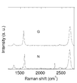
図7は、このようにして得られたグラフェンからのラマン散乱スペクトルである。生成核からのスペクトル(N)の2700cm-1近傍の2Dバンドのピークと1590cm-1近傍のGバンドのピークの強度比(2D/G比=I2D/IG)は1を下回っており、多層のグラフェンとなっているものと思われる。一方、生成核の周りに成長したグラフェン領域からのスペクトル(G)の2D/G比は2.5を超えており、極めて高い単層性のグラフェンであることが確認できる。
また、生成核の周りに成長したグラフェン領域からのスペクトルの1590cm-1近傍のGバンドのピークと1300cm-1近傍のDバンドのピークの強度比(G/D比=IG/ID)は3程度であった。
なお、膜の全面から、これと同様のラマンスペクトルが得られている。
[100℃で合成されたグラフェンのラマンスペクトル]
基板として、0.2°のオフ角を有するサファイヤ基板(1cm×1cm)を用いた。事前に表面の不純物を除去すべく、酸素プラズマアッシングによる清浄化処理を施し、このサファイヤ基板の主面にガリウム金属を載置して、図1(a)に図示したように、石英管の内部に挿入した。そして、Arガスをキャリアガスとして流しながらRF加熱して基板温度を850℃まで昇温し、この温度で保持してガリウムを融解させた。
基板として、0.2°のオフ角を有するサファイヤ基板(1cm×1cm)を用いた。事前に表面の不純物を除去すべく、酸素プラズマアッシングによる清浄化処理を施し、このサファイヤ基板の主面にガリウム金属を載置して、図1(a)に図示したように、石英管の内部に挿入した。そして、Arガスをキャリアガスとして流しながらRF加熱して基板温度を850℃まで昇温し、この温度で保持してガリウムを融解させた。
次いで、Arガスを200sccmとCH4ガスを1sccmの流量(0.5気圧)で流し、基板を1050℃まで急加熱して5分間保持した。その後、CH4ガスの供給を停止し、Arガス雰囲気中で室温まで冷却した。
これに続き、Arガスをキャリアガスとして流しながらRF加熱して基板温度を100℃まで昇温し、Arガスを200sccmとCH4ガスを1sccmの流量(0.5気圧)で流し、基板温度100℃で60分間保持した。その後、CH4ガスの供給を停止し、Arガス雰囲気中で室温まで冷却した。
図8は、このようにして得られたグラフェンからのラマン散乱スペクトルである。生成核の周りに成長したグラフェン領域からのスペクトル(G)の2700cm-1近傍の2Dバンドのピークと1590cm-1近傍のGバンドのピークの強度比(2D/G比=I2D/IG)は1を上回っており、1~2層のグラフェンが形成されているものと推測される。
また、生成核の周りに成長したグラフェン領域からのスペクトルの1590cm-1近傍のGバンドのピークと1300cm-1近傍のDバンドのピークの強度比(G/D比=IG/ID)は10程度であり、欠陥の少ない膜であると評価してよい。
なお、膜の全面から、これと同様のラマンスペクトルが得られている。
上述のとおり、本発明によれば、大面積かつ高品質の単層グラフェンの低温合成技術が提供される。
Claims (28)
- 基板の主面に炭素六員環の生成核を形成する第1の工程と、
前記生成核の周りで2次元的に炭素六員環を形成してグラフェン膜とする第2の工程を備え、
前記第2の工程における炭素六員環の形成を300℃以下の温度で実行する、グラフェンの製造方法。 - 前記第1の工程において、前記基板の主面に融点が400℃以下の金属の液滴を接触させた状態で炭化水素を含有するガスを供給し、前記基板の主面と前記金属との接触面に前記生成核を形成する、請求項1に記載のグラフェンの製造方法。
- 前記融点が400℃以下の金属は、ガリウム、インジウム、ガリウム-インジウム合金の群から選択される少なくとも1種である、請求項2に記載のグラフェンの製造方法。
- 前記第1の工程における生成核の形成を、フォトリソグラフィ法により予め前記基板の主面に配列されたアモルファス炭素の核を形成しておき、該基板の主面に液体ガリウムを接触させた状態で熱処理して実行する、請求項1に記載のグラフェンの製造方法。
- 前記第1の工程で形成される生成核は、剥離法により形成された炭素六員環である、請求項1に記載のグラフェンの製造方法。
- 前記第2の工程において、前記生成核が形成された基板の主面領域にグラフェン合成の触媒作用を有する金属であって融点が400℃以下の金属を接触させた状態で炭化水素を含有するガスを供給し、前記基板の主面と前記金属との接触界面から前記炭素六員環を形成させてグラフェン膜とする、請求項1~5の何れか1項に記載のグラフェンの製造方法。
- 前記触媒作用を有する金属として前記炭素六員環の形成温度よりも低い融点を有する金属を選択し、該金属の液滴を前記基板の主面領域に接触させた状態で前記炭素六員環を形成させる、請求項6に記載のグラフェンの製造方法。
- 前記融点が400℃以下の金属は、ガリウム、インジウム、ガリウム-インジウム合金の群から選択される少なくとも1種である、請求項6または7に記載のグラフェンの製造方法。
- 前記炭化水素を含有するガスをプラズマ化して供給する、請求項2~8の何れか1項に記載のグラフェンの製造方法。
- 基板の主面に炭素六員環の生成核を形成する第1の工程と、
前記生成核を形成した基板の主面に、グラフェン合成の触媒作用を有する金属であって融点が400℃以下の金属を接触させ、該金属を融点を超える温度に保持した状態で炭化水素を含有するガスを供給し、前記基板主面の金属との接触界面にグラフェンを成長させる第2の工程と、
を備えているグラフェンの製造方法。 - 前記融点が400℃以下の金属は、ガリウム、インジウム、ガリウム-インジウム合金の群から選択される少なくとも1種である、請求項10に記載のグラフェンの製造方法。
- 前記第1の工程は、前記基板を1000℃以上の温度に保持した状態で炭化水素を含有するガスを供給して実行される、請求項10または11に記載のグラフェンの製造方法。
- 前記第1の工程は、前記基板の主面に、グラフェン合成の触媒作用を有する金属であって融点が1000℃未満の金属を接触させた状態で前記炭化水素を含有するガスを供給して実行される、請求項10に記載のグラフェンの製造方法。
- 前記融点が1000℃未満の金属は、ガリウム、インジウム、アンチモンおよびそれらの合金の群から選択される少なくとも1種である、請求項13に記載のグラフェンの製造方法。
- 前記第1の工程は、剥離法により前記基板の主面にグラファイト若しくはグラフェンを転写して実行される、請求項10または11に記載のグラフェンの製造方法。
- 前記第1の工程は、フォトリソグラフ法により前記基板の主面にグラファイト若しくはグラフェンをパターニングして実行される、請求項10または11に記載のグラフェンの製造方法。
- 前記第2の工程は、プラズマアシスト法により前記炭化水素ガスの分解効率を高めて実行される、請求項10~16の何れか1項に記載のグラフェンの製造方法。
- 前記第2の工程は、融点が400℃以下の金属としてガリウムを選択し、300℃以下の温度で実行される、請求項10~17の何れか1項に記載のグラフェンの製造方法。
- 前記第2の工程に続き、前記基板から前記グラフェンを分離する第3の工程を備えている、請求項10~18の何れか1項に記載のグラフェンの製造方法。
- 前記基板はオフ角の絶対値が30°以内の(0001)面(C面)を主面とするサファイヤである、請求項10~19の何れか1項に記載のグラフェンの製造方法。
- 基板主面に形成されたレジストパターンに、グラフェン合成の触媒作用を有する金属であって融点が400℃以下の金属を接触させ、該金属を融点を超える温度に保持した状態で炭化水素を含有するガスを供給し、前記基板主面の金属との接触界面にグラフェンを成長させ、前記レジストパターンをグラフェン化して回路を形成する工程を含むことを特徴とする電子素子の製造方法。
- 前記融点が400℃以下の金属は、ガリウム、インジウム、およびそれらの合金の群から選択される少なくとも1種である、請求項21に記載の電子素子の製造方法。
- 炭素六員環の集合からなる複数のドメインから構成され、前記複数のドメインのそれぞれは、該ドメイン内に前記炭素六員環の生成核を有し、その密度が1×106cm-2以下である、グラフェン。
- 前記ドメイン内の炭素六員環の方位がグラフェン膜の少なくとも10-7cm2の範囲内で実質的に同一であり、1×10⁻⁷cm2以上の面積を有する連続膜であり、実質的に単層の膜である、請求項23に記載のグラフェン。
- 前記グラフェンから得られるラマン散乱スペクトル中に認められる2700cm-1近傍の2Dバンドのピークと1590cm-1近傍のGバンドのピークの強度比(2D/G比=I2D/IG)が1以上である、請求項23または24に記載のグラフェン。
- 前記グラフェンから得られるラマン散乱スペクトル中に認められる1590cm-1近傍のGバンドのピークと1300cm-1近傍のDバンドのピークの強度比(G/D比=IG/ID)が3以上である、請求項23~25の何れか1項に記載のグラフェン。
- 請求項23~26の何れか1項に記載のグラフェンを備えた電子素子。
- 前記グラフェンから成るチャネル領域を有する、請求項27に記載の電子素子。
Priority Applications (1)
| Application Number | Priority Date | Filing Date | Title |
|---|---|---|---|
| JP2017515549A JP6754355B2 (ja) | 2015-04-28 | 2016-04-26 | グラフェンおよび電子素子ならびにこれらの製造方法 |
Applications Claiming Priority (2)
| Application Number | Priority Date | Filing Date | Title |
|---|---|---|---|
| JP2015-091999 | 2015-04-28 | ||
| JP2015091999 | 2015-04-28 |
Publications (1)
| Publication Number | Publication Date |
|---|---|
| WO2016175195A1 true WO2016175195A1 (ja) | 2016-11-03 |
Family
ID=57198472
Family Applications (1)
| Application Number | Title | Priority Date | Filing Date |
|---|---|---|---|
| PCT/JP2016/063014 Ceased WO2016175195A1 (ja) | 2015-04-28 | 2016-04-26 | グラフェンおよび電子素子ならびにこれらの製造方法 |
Country Status (2)
| Country | Link |
|---|---|
| JP (1) | JP6754355B2 (ja) |
| WO (1) | WO2016175195A1 (ja) |
Cited By (9)
| Publication number | Priority date | Publication date | Assignee | Title |
|---|---|---|---|---|
| WO2017034018A1 (ja) * | 2015-08-26 | 2017-03-02 | 並木精密宝石株式会社 | グラフェン膜、複合体、それらの製造方法、及び単結晶サファイア基板 |
| JP2018188329A (ja) * | 2017-05-02 | 2018-11-29 | 学校法人 名城大学 | 構造体 |
| WO2019070872A1 (en) * | 2017-10-03 | 2019-04-11 | Northwestern University | INTERFACIAL BARRIERS IN GRAPHIC CONDUCTOR FOR ELECTRONIC DEVICES BASED ON LIQUID METAL |
| KR20200044072A (ko) * | 2017-08-22 | 2020-04-28 | 테르마 코퍼레이션 | 그래핀 나노리본, 그래핀 나노 플레이틀렛 및 이들의 혼합물 그리고 합성 방법 |
| CN112730558A (zh) * | 2020-12-24 | 2021-04-30 | 宁波材料所杭州湾研究院 | 一种基于金刚石/石墨烯异质结的耐超声电极及其制备方法 |
| JP2022521587A (ja) * | 2019-02-20 | 2022-04-11 | ピーピージー・インダストリーズ・オハイオ・インコーポレイテッド | グラフェン炭素ナノ粒子及び分散剤樹脂を含有する分散液 |
| JP2023086331A (ja) * | 2021-12-10 | 2023-06-22 | 日本碍子株式会社 | ガス反応方法およびガス反応装置 |
| US12371326B2 (en) | 2021-12-22 | 2025-07-29 | Nabors Energy Transition Solutions Llc | Sulfur doped carbon-based nanomaterial and methods of forming the same |
| US12606441B2 (en) | 2022-03-04 | 2026-04-21 | Nabors Energy Transition Solutions Llc | Boron doped carbon-based nanomaterial and methods of forming the same |
Families Citing this family (1)
| Publication number | Priority date | Publication date | Assignee | Title |
|---|---|---|---|---|
| CN114921676B (zh) * | 2022-05-27 | 2023-03-24 | 江阴镓力材料科技有限公司 | 一种液态金属原位复合石墨烯热界面材料及其制备方法 |
Citations (2)
| Publication number | Priority date | Publication date | Assignee | Title |
|---|---|---|---|---|
| JP2013177273A (ja) * | 2012-02-28 | 2013-09-09 | Kyushu Univ | グラフェン薄膜の製造方法及びグラフェン薄膜 |
| JP2015024937A (ja) * | 2013-07-26 | 2015-02-05 | 住友電気工業株式会社 | グラファイト膜の製造方法およびグラファイト構造体 |
Family Cites Families (1)
| Publication number | Priority date | Publication date | Assignee | Title |
|---|---|---|---|---|
| WO2014110170A1 (en) * | 2013-01-09 | 2014-07-17 | The Regents Of The University Of California | Chemical vapor deposition growth of graphene |
-
2016
- 2016-04-26 JP JP2017515549A patent/JP6754355B2/ja active Active
- 2016-04-26 WO PCT/JP2016/063014 patent/WO2016175195A1/ja not_active Ceased
Patent Citations (2)
| Publication number | Priority date | Publication date | Assignee | Title |
|---|---|---|---|---|
| JP2013177273A (ja) * | 2012-02-28 | 2013-09-09 | Kyushu Univ | グラフェン薄膜の製造方法及びグラフェン薄膜 |
| JP2015024937A (ja) * | 2013-07-26 | 2015-02-05 | 住友電気工業株式会社 | グラファイト膜の製造方法およびグラファイト構造体 |
Non-Patent Citations (6)
| Title |
|---|
| CHAN, SHIH-HAO ET AL.: "Low-temperature synthesis of graphene on Cu using plasma- assisted thermal chemical vapor deposition", NANOSCALE RESEARCH LETTERS, vol. 8, no. 285, 12 July 2013 (2013-07-12), pages 1 - 5, XP055326857 * |
| DING, GUQIAO ET AL.: "Chemical vapor deposition of graphene on liquid metal catalysts", CARBON, vol. 53, 17 November 2012 (2012-11-17), pages 321 - 326, XP055104265 * |
| TAKAKI HIYAMA ET AL.: "CVD-ho o Mochiita Ekitai Gallium Shokubai Kaimen ni Okeru Graphene Gosei", THE 62ND JSAP SPRING MEETING KOEN YOKOSHU, 26 February 2015 (2015-02-26), pages 12P-D7 - 9 * |
| WANG, JIAO ET AL.: "High-mobility graphene on liquid p-block elements by ultra-low-loss CVD growth", SCIENTIFIC REPORTS, vol. 3, no. 2670, 16 September 2013 (2013-09-16), pages 1 - 7, XP055234692 * |
| WANG, S.M. ET AL.: "A novel semiconductor compatible path for nano-graphene synthesis using CBr4 precursor and Ga catalyst", SCIENTIFIC REPORTS, vol. 4, no. 4653, pages 1 - 7, XP055326716 * |
| YOSUKE MIYAZAWA ET AL.: "Ekitai Gallium o Mochiita Resist Pattern kara no Graphene FET Keisei", 2010 NEN AUTUMN THE 71ST EXTENDED ABSTRACTS, THE JAPAN SOCIETY OF APPLIED PHYSICS, 30 August 2010 (2010-08-30) * |
Cited By (14)
| Publication number | Priority date | Publication date | Assignee | Title |
|---|---|---|---|---|
| WO2017034018A1 (ja) * | 2015-08-26 | 2017-03-02 | 並木精密宝石株式会社 | グラフェン膜、複合体、それらの製造方法、及び単結晶サファイア基板 |
| JP2018188329A (ja) * | 2017-05-02 | 2018-11-29 | 学校法人 名城大学 | 構造体 |
| KR102369636B1 (ko) | 2017-08-22 | 2022-03-03 | 테르마 코퍼레이션 | 그래핀 나노리본, 그래핀 나노 플레이틀렛 및 이들의 혼합물 그리고 합성 방법 |
| KR20200044072A (ko) * | 2017-08-22 | 2020-04-28 | 테르마 코퍼레이션 | 그래핀 나노리본, 그래핀 나노 플레이틀렛 및 이들의 혼합물 그리고 합성 방법 |
| US11057994B2 (en) | 2017-10-03 | 2021-07-06 | Northwestern University | Conductive graphene interfacial barriers for liquid metal electronics |
| WO2019070872A1 (en) * | 2017-10-03 | 2019-04-11 | Northwestern University | INTERFACIAL BARRIERS IN GRAPHIC CONDUCTOR FOR ELECTRONIC DEVICES BASED ON LIQUID METAL |
| JP2022521587A (ja) * | 2019-02-20 | 2022-04-11 | ピーピージー・インダストリーズ・オハイオ・インコーポレイテッド | グラフェン炭素ナノ粒子及び分散剤樹脂を含有する分散液 |
| JP7447135B2 (ja) | 2019-02-20 | 2024-03-11 | ピーピージー・インダストリーズ・オハイオ・インコーポレイテッド | グラフェン炭素ナノ粒子及び分散剤樹脂を含有する分散液 |
| CN112730558A (zh) * | 2020-12-24 | 2021-04-30 | 宁波材料所杭州湾研究院 | 一种基于金刚石/石墨烯异质结的耐超声电极及其制备方法 |
| CN112730558B (zh) * | 2020-12-24 | 2023-10-31 | 宁波材料所杭州湾研究院 | 一种基于金刚石/石墨烯异质结的耐超声电极及其制备方法 |
| JP2023086331A (ja) * | 2021-12-10 | 2023-06-22 | 日本碍子株式会社 | ガス反応方法およびガス反応装置 |
| JP7719708B2 (ja) | 2021-12-10 | 2025-08-06 | 日本碍子株式会社 | ガス反応方法およびガス反応装置 |
| US12371326B2 (en) | 2021-12-22 | 2025-07-29 | Nabors Energy Transition Solutions Llc | Sulfur doped carbon-based nanomaterial and methods of forming the same |
| US12606441B2 (en) | 2022-03-04 | 2026-04-21 | Nabors Energy Transition Solutions Llc | Boron doped carbon-based nanomaterial and methods of forming the same |
Also Published As
| Publication number | Publication date |
|---|---|
| JPWO2016175195A1 (ja) | 2018-02-22 |
| JP6754355B2 (ja) | 2020-09-09 |
Similar Documents
| Publication | Publication Date | Title |
|---|---|---|
| JP6754355B2 (ja) | グラフェンおよび電子素子ならびにこれらの製造方法 | |
| EP2412670B1 (en) | Method for producing graphene film, method for manufacturing electronic element, and method for transferring graphene film to substrate | |
| Khan et al. | Direct CVD growth of graphene on technologically important dielectric and semiconducting substrates | |
| Bayer et al. | Atomic-scale in situ observations of crystallization and restructuring processes in two-dimensional MoS2 films | |
| KR101611410B1 (ko) | 그래핀의 제조 방법 | |
| Huang et al. | Epitaxial growth of graphene on silicon carbide (SiC) | |
| Pan et al. | Transfer-free growth of graphene on SiO2 insulator substrate from sputtered carbon and nickel films | |
| Galbiati et al. | Group-IV 2D materials beyond graphene on nonmetal substrates: Challenges, recent progress, and future perspectives | |
| US20100021708A1 (en) | Large-Area Single- and Few-Layer Graphene on Arbitrary Substrates | |
| US20120021224A1 (en) | Graphene/graphene oxide platelet composite membranes and methods and devices thereof | |
| Saito et al. | Direct growth of graphene films on sapphire (0001) and (1120) surfaces by self-catalytic chemical vapor deposition | |
| CN102849961A (zh) | 在基板上成长碳薄膜或无机材料薄膜的方法 | |
| US20190139762A1 (en) | Epitaxial growth of defect-free, wafer-scale single-layer graphene on thin films of cobalt | |
| Kitaura et al. | Chemical vapor deposition growth of graphene and related materials | |
| Yang et al. | Recent advances in preparation, properties and device applications of two-dimensional h-BN and its vertical heterostructures | |
| Puybaret et al. | Nanoselective area growth of GaN by metalorganic vapor phase epitaxy on 4H-SiC using epitaxial graphene as a mask | |
| Hiura et al. | Liquid phase growth of graphene on silicon carbide | |
| Rafique et al. | Synthesis and characterization of Ga2O3 nanosheets on 3C-SiC-on-Si by low pressure chemical vapor deposition | |
| Niu et al. | Atomic mechanism for the growth of wafer-scale single-crystal graphene: theoretical perspective and scanning tunneling microscopy investigations | |
| Kwieciñski et al. | Chemical vapor deposition growth of bilayer graphene in between molybdenum disulfide sheets | |
| Ago et al. | Step-templated CVD growth of aligned graphene nanoribbons supported by a single-layer graphene film | |
| Olson et al. | Low-temperature chemical vapor deposition growth of graphene films enabled by ultrathin alloy catalysts | |
| CN117684130A (zh) | 多孔石墨烯半导体的制备方法 | |
| Berger et al. | Epitaxial Graphene on SiC: 2D Sheets, Selective Growth, and Nanoribbons | |
| Jiao et al. | High quality graphene formation on 3C-SiC/4H-AlN/Si heterostructure |
Legal Events
| Date | Code | Title | Description |
|---|---|---|---|
| 121 | Ep: the epo has been informed by wipo that ep was designated in this application |
Ref document number: 16786472 Country of ref document: EP Kind code of ref document: A1 |
|
| ENP | Entry into the national phase |
Ref document number: 2017515549 Country of ref document: JP Kind code of ref document: A |
|
| NENP | Non-entry into the national phase |
Ref country code: DE |
|
| 122 | Ep: pct application non-entry in european phase |
Ref document number: 16786472 Country of ref document: EP Kind code of ref document: A1 |