WO2016171262A1 - イオンビーム照射装置およびイオンビーム照射方法 - Google Patents
イオンビーム照射装置およびイオンビーム照射方法 Download PDFInfo
- Publication number
- WO2016171262A1 WO2016171262A1 PCT/JP2016/062798 JP2016062798W WO2016171262A1 WO 2016171262 A1 WO2016171262 A1 WO 2016171262A1 JP 2016062798 W JP2016062798 W JP 2016062798W WO 2016171262 A1 WO2016171262 A1 WO 2016171262A1
- Authority
- WO
- WIPO (PCT)
- Prior art keywords
- substrate
- ion beam
- scan
- beam irradiation
- current density
- Prior art date
- Legal status (The legal status is an assumption and is not a legal conclusion. Google has not performed a legal analysis and makes no representation as to the accuracy of the status listed.)
- Ceased
Links
Images







Classifications
-
- H—ELECTRICITY
- H01—ELECTRIC ELEMENTS
- H01J—ELECTRIC DISCHARGE TUBES OR DISCHARGE LAMPS
- H01J37/00—Discharge tubes with provision for introducing objects or material to be exposed to the discharge, e.g. for the purpose of examination or processing thereof
- H01J37/30—Electron-beam or ion-beam tubes for localised treatment of objects
-
- H—ELECTRICITY
- H01—ELECTRIC ELEMENTS
- H01J—ELECTRIC DISCHARGE TUBES OR DISCHARGE LAMPS
- H01J37/00—Discharge tubes with provision for introducing objects or material to be exposed to the discharge, e.g. for the purpose of examination or processing thereof
- H01J37/30—Electron-beam or ion-beam tubes for localised treatment of objects
- H01J37/305—Electron-beam or ion-beam tubes for localised treatment of objects for casting, melting, evaporating, or etching
-
- H—ELECTRICITY
- H01—ELECTRIC ELEMENTS
- H01J—ELECTRIC DISCHARGE TUBES OR DISCHARGE LAMPS
- H01J37/00—Discharge tubes with provision for introducing objects or material to be exposed to the discharge, e.g. for the purpose of examination or processing thereof
- H01J37/30—Electron-beam or ion-beam tubes for localised treatment of objects
- H01J37/317—Electron-beam or ion-beam tubes for localised treatment of objects for changing properties of the objects or for applying thin layers thereon, e.g. for ion implantation
Definitions
- the present invention relates to an ion beam irradiation apparatus and an ion beam irradiation method for processing a substrate by irradiating the substrate with an ion beam in a vacuum atmosphere, such as an ion milling apparatus and an ion implantation apparatus.
- An ion source that extracts an ion beam having a rectangular cross section whose long side is larger than that of the substrate and whose short side is smaller than that of the substrate, and the substrate is placed on the ion beam so that the substrate is positioned inside and outside the ion beam irradiation region. It has a translation mechanism that translates in the short side direction and a rotation mechanism that rotates the substrate around its center when the substrate is outside the ion beam irradiation area.
- a processing apparatus and a processing method for performing processing are described in Patent Document 1, for example.
- the present invention provides an ion beam irradiation apparatus that can irradiate the entire surface of an ion beam with an ion beam and that can reduce the time required for substrate processing even when the substrate is mechanically scanned and rotated.
- an ion beam irradiation apparatus that can irradiate the entire surface of an ion beam with an ion beam and that can reduce the time required for substrate processing even when the substrate is mechanically scanned and rotated.
- Another object is to provide an ion beam irradiation method capable of performing the above-described processing.
- An ion beam irradiation apparatus is an apparatus that irradiates a substrate with an ion beam in a vacuum atmosphere, and a vacuum container that is evacuated to a vacuum, a holder that is accommodated in the vacuum container and holds the substrate, A rotation mechanism for rotating the holder and the substrate held by the holder around a center portion of the substrate, a scanning mechanism for mechanically reciprocatingly scanning the holder, the substrate held by the substrate and the rotation mechanism, and the holder.
- An ion beam supply unit that irradiates an ion beam having a size larger than a size including a region where the substrate and the substrate are scanned with respect to the held substrate, the rotation mechanism, The scanning mechanism is controlled to rotate and scan the substrate within the ion beam irradiation area, thereby And a control unit which has a function of irradiating an ion beam, and characterized in that.
- the ion beam irradiation apparatus irradiates the substrate held by the holder with an ion beam having a size larger than the size of the substrate and the region including the region where the substrate is scanned.
- the ion beam supply unit, the rotation mechanism, and the scanning mechanism are controlled to rotate and scan the substrate within the ion beam irradiation region, thereby irradiating the entire surface of the substrate with the ion beam.
- a controller that scans the substrate within the ion beam irradiation region, and it is not necessary to move the substrate outside the ion beam irradiation region for each substrate scan as in the prior art.
- the processing time of the substrate can be improved by shortening the time required for the substrate processing.
- the substrate is also rotated in the ion beam irradiation area, and it is not necessary to move the substrate outside the ion beam irradiation area every time the substrate is rotated as in the prior art. Also from this point of view, it is possible to shorten the time required for the substrate processing and improve the substrate processing efficiency.
- the ion beam supply unit is an ion source having a plasma generation unit that generates plasma and an extraction electrode system that extracts an ion beam from the plasma by the action of an electric field, and the extraction electrode system includes the substrate and the ion source
- a configuration in which an ion beam extraction region having a size larger than a size including a region to be scanned by the substrate may be employed. Moreover, you may employ
- the ion beam supply unit includes a plasma generation unit that generates plasma and an extraction electrode system that extracts an ion beam from the plasma by the action of an electric field, and the extraction electrode system is not extracted from a region from which the ion beam is extracted.
- the areas are arranged at a predetermined cycle, and the direction of scanning by the scanning mechanism is parallel or oblique to the arrangement direction of the two kinds of areas of the extraction electrode system. You may employ
- the control device may further have a function of controlling the scan width of the substrate to be equal to or less than the cycle (not including 0) based on the cycle of the extraction electrode system.
- the control device further has a function of obtaining a scan width that minimizes a difference between a maximum value and a minimum value of the ion beam irradiation amount on the substrate and setting the scan width of the substrate to the obtained scan width. May be.
- a beam measuring device that measures the current density distribution of the ion beam in the scan direction of the substrate may be provided, and the current density distribution measured by the beam measuring device may be used for controlling the scan width of the substrate.
- An ion beam irradiation method is a method of irradiating a substrate with an ion beam in a vacuum atmosphere, a vacuum container that is evacuated to a vacuum, a holder that is accommodated in the vacuum container and holds the substrate, A rotation mechanism for rotating the holder and the substrate held by the holder around a center portion of the substrate, a scanning mechanism for mechanically reciprocatingly scanning the holder, the substrate held by the substrate and the rotation mechanism, and the holder.
- An ion beam supply unit that irradiates an ion beam having a size larger than a size including a region where the substrate and the substrate are scanned with respect to the held substrate.
- the substrate is rotated and scanned within the ion beam irradiation region, and the entire surface of the substrate is It is characterized by irradiating the ion beam.
- An ion beam irradiation method is a method of irradiating a substrate with an ion beam in a vacuum atmosphere, a vacuum container that is evacuated to a vacuum, a holder that is accommodated in the vacuum container and holds the substrate, An ion source that irradiates a substrate held by the holder with a plasma generation unit that generates plasma and an extraction electrode system that extracts an ion beam from the plasma by the action of an electric field,
- the extraction electrode system includes an ion source in which an ion beam extraction region and an ion beam extraction region are alternately arranged in a predetermined direction at a predetermined cycle, the holder, and a substrate held by the holder.
- a scanning mechanism that mechanically reciprocates in a direction parallel or oblique to the arrangement direction of the two types of regions of the extraction electrode system; And the ion source has an ion beam having a size larger than a size of the substrate and a region where the substrate is scanned with respect to the substrate held by the holder.
- the substrate is scanned in accordance with a scan waveform in which a scan position continuously changes with time using an ion beam irradiation apparatus configured to irradiate the ion beam. It is characterized by irradiating the entire surface with an ion beam.
- the entire surface of the substrate can be irradiated with an ion beam, and the time required for substrate processing can be reduced even if the substrate is mechanically scanned and rotated.
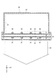
- FIG. 1 shows an embodiment of an ion beam irradiation apparatus according to the present invention.
- the X direction, the Y direction, and the Z direction that are orthogonal to each other at one point are illustrated in each drawing.
- the Y direction and the Z direction are horizontal directions
- the X direction is a vertical direction.
- the ion beam 28 travels in the Z direction in this example.
- This ion beam irradiation apparatus is an apparatus that irradiates a substrate 6 with an ion beam 28 in a vacuum atmosphere, and is accommodated in a vacuum container 4 that is evacuated to vacuum by a vacuum evacuation apparatus (not shown).
- An example of the rotation direction C is shown in the figure, but it may be in the opposite direction. Further, the rotation of the holder 8 and the substrate 6 by the rotation mechanism 10 may be continuous rotation or step rotation for each predetermined angle.
- the substrate 6 is, for example, a semiconductor substrate such as a silicon wafer, or a substrate in which a film such as a magnetic film is formed on the surface of the semiconductor substrate, but is not limited thereto.
- the shape of the substrate 6 is, for example, a circle (including an orientation flat or a notch in a part of the circumference), but is not limited thereto.
- the ion beam irradiation apparatus further includes a tilt mechanism 12 that tilts the holder 8 and the substrate 6 held by the holder 8 to change the tilt angle (tilt angle) ⁇ of the substrate 6 with respect to the ion beam 28.
- the change of the tilt angle ⁇ by the tilt mechanism 12 may be performed within the irradiation region of the ion beam 28 or may be performed outside the irradiation region.
- the tilt mechanism 12 is not essential to the present invention.
- the ion beam irradiation apparatus further includes a plasma generation unit 22 that generates the plasma 23 and an extraction electrode system 24 that extracts the ion beam 28 from the plasma 23 by the action of an electric field.
- the ion beam 28 is extracted from the holder 8.
- An ion source 20 for irradiating the substrate 6 held on the substrate is provided.
- the ion source 20 may be disposed inside the vacuum container 4 together with the extraction electrode system 24 or may be disposed outside the vacuum container 4.
- the extraction electrode system 24 has a predetermined direction (in this embodiment, X 1) a region A 1 from which the ion beam 28 is extracted and a region B 1 from which the ion beam 28 is not extracted. It has a structure obtained by alternately arranged at a predetermined period P 1 in the direction).
- the extraction electrode system 24 will be further described later.
- This ion beam irradiation apparatus further includes a scanning mechanism for mechanically reciprocatingly scanning the holder 8, the substrate 6 held thereon, the rotation mechanism 10 and the tilt mechanism 12 via the shaft 16 (that is, mechanical reciprocating scanning). 14 is provided.
- the scan by the scan mechanism 14 is, for example, linear.
- An example of the scanning direction D in that case is shown in the drawing.
- the scanning mechanism 14 is provided outside the vacuum container 4 in this example, but is not limited thereto.
- the scanning direction D of the holder 8 and the substrate 6 by the scanning mechanism 14 is a direction parallel to the arrangement direction (X direction) of the two types of regions A 1 and B 1 of the extraction electrode system 24.
- the direction may be oblique with respect to the arrangement direction of the two types of regions A 1 and B 1 of the extraction electrode system 24.
- the size at the position of the substrate 6 includes the substrate 6 and a region where the substrate 6 is scanned, as in the example shown in FIG. 2.
- Figure 2 also shows an example of a scan direction D and the scan width W S of the substrate 6. That is, an example in which the substrate 6 indicated by a broken line in FIG. 2 is located at one end of the scan and the substrate 6 indicated by a two-dot chain line is located at the other end of the scan is shown.
- the type of the ion source 20 is not limited to a specific type.
- the ion source 20 may be a so-called bucket type ion source (also called a multipole magnetic field type ion source) that performs confinement of the plasma 23 using a multipolar magnetic field (cusp magnetic field), or
- a high-frequency ion source that generates plasma 23 by high-frequency discharge may be used.
- An ion source may be used.
- the number of electrodes constituting the extraction electrode system 24 is not limited to a specific one.
- the bucket ion source (a) has an advantage that, for example, the plasma 23 having a large area and good uniformity can be generated, and the ion beam 28 having a large area and good uniformity can be easily extracted. ing.
- the high-frequency ion source (b) has an advantage that, for example, heat input to the electrodes constituting the extraction electrode system 24 is small.
- the extraction direction of the ion beam 28 from the ion source 20 is a direction that intersects the gravity direction G (for example, a direction that is substantially orthogonal or oblique as in the example shown in FIG. 1). .
- the substrate 6 it is not necessary to place the substrate 6 directly under the ion source 20, and even if foreign matter (dust) such as a peeling piece of a deposit inside the ion source 20 falls from the ion source 20, it is mixed into the substrate 6. It becomes difficult. As a result, it is possible to suppress the occurrence of processing defects of the substrate 6 due to foreign matter contamination.
- the plasma generation unit 22 that generates the plasma 23 is a known plasma generation unit that constitutes, for example, the above-described bucket ion source, high-frequency ion source, or Bernas ion source, and is simplified in FIG. .
- the ion source 20 in the example shown in FIG. 3 has a plurality of (three in this example) electrodes 31 to 33 as a component of the extraction electrode system 24.
- the electrode closest to the plasma 23 is referred to as the plasma electrode 31, and the electrode on the downstream side (downstream in the traveling direction of the ion beam 28, hereinafter the same) is referred to as the extraction electrode 32.
- the downstream electrode is called a ground electrode 33.
- a positive acceleration voltage is applied to the plasma electrode 31 from a DC power source (not shown).
- a positive extraction voltage lower than the potential of the plasma electrode 31 is applied to the extraction electrode 32 from a DC power source (not shown).
- the ground electrode 33 is electrically grounded.
- the extraction electrode system 24, more specifically, each of the electrodes 31 to 33, in this embodiment, has an ion beam extraction region 26 (with a size larger than the size including the substrate 6 and the region in which the substrate 6 is scanned). 4 and FIG. 5).
- the ion beam extraction region 26 is a region having a number of openings (ion extraction openings) such as holes and slits through which the ion beam 28 is extracted.
- the ion beam extraction region 26 shown in FIG. 4 has a large number of holes 34
- the ion beam extraction region 26 shown in FIG. 5 has a large number of slits 37.
- the scan width W S is 80 mm
- height and width of the ion beam extraction region 26 is 400 mm ⁇ 400 mm. However, it is not limited to this.
- the three electrodes 31 to 33 have substantially the same configuration except for the cooling pipes 40 and 41. Therefore, the ion electrode extraction region 26 portion is represented by the plasma electrode 31.
- the plan view is shown in FIG. 4 or FIG.
- Each of the electrodes 31 to 33 may have a large number of holes 34 for extracting the ion beam 28 as in the examples shown in FIGS. 3 and 4, or the ion beam 28 as in the example shown in FIG. You may have many slits 37 for drawer
- the plasma electrode 31 may be provided with a cooling pipe for cooling the electrode in the electrode constituting the extraction electrode system 24.
- a plurality of cooling pipes 40 are arranged on the plasma electrode 31 at a constant pitch in the X direction.
- a coolant such as cooling water flows. Since the ion beam 28 is not extracted from the portion where the cooling pipe 40 is provided, the extraction electrode system 24 includes a plurality of holes 34 (see FIG. 4) or a plurality of slits 37 (see FIG. 4).
- a cooling pipe for cooling the electrode may be provided on the electrode downstream of the plasma electrode 31 as necessary.
- the extraction electrode 32 is also provided with a plurality of cooling pipes 41.
- Each cooling pipe 41 is arranged corresponding to the position of each cooling pipe 40 in this example.
- a coolant such as cooling water flows.
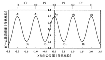
- FIG. 1 An example of the current density distribution at the position of the substrate 6 of the ion beam 28 extracted from the ion source 20 including the extraction electrode system 24 having the two types of regions A 1 and B 1 as described above is shown in FIG.
- the current density distribution is pulsating at a constant period P 2.
- the peak portion A 2 is a portion corresponding to the region A 1 where the ion beam of the extraction electrode system 24 is extracted, and the valley portion B 2 is a portion corresponding to the region B 1 where the ion beam of the extraction electrode system 24 is not extracted.
- the relationship between the period P 2 and the period P 1 of the extraction electrode system 24 is a special case except (for example, dispersion of the ion beam 28 is large), can often be considered as P 1 ⁇ P 2 .
- the current density distribution shown in FIG. 6 is only an example, and the width relationship between the two regions A 1 and B 1 of the extraction electrode system 24 and the ion beam extracted from each hole and slit in each region A 1 .
- a current density distribution with smaller pulsation, a current density distribution with larger pulsation, and other current density distributions can be realized depending on the divergence angle. For example, see FIG.
- the plasma electrode 31 Since the plasma electrode 31 has the largest heat input from the plasma generation unit 22, in order to further increase the cooling capacity thereof, the plasma electrode 31 is cooled in parallel with the cooling pipe 40 in the middle of the region A 1 from which each ion beam is extracted. A cooling pipe thinner than the pipe 40 may be further arranged. Even in such a case, it can be said that the basic period of the region A 1 taken large is still P 1 . If the additional cooling pipe is arranged, the ion beam is not drawn out from the cooling pipe portion. Therefore, each peak portion of the current density distribution of the ion beam 28, for example, each peak of the current density distribution shown in FIG. Although the portion A 2 has two peaks, it can be said that the basic (ie, greatly regarded) period of the beam current density distribution is still P 2 .
- the extraction electrode system 24 of the ion source 20 may have a split structure electrode on at least one of the electrodes constituting the extraction electrode system 24.
- the electrode having a divided structure here refers to a plurality of electrode pieces each having a number of ion extraction openings (for example, openings corresponding to the holes 34 or the slits 37) in a predetermined direction (for example, FIG. 4). It has a connecting portion extending in the (Y direction), and is arranged in a predetermined cycle (for example, the X direction) with a predetermined period to be connected to form one electrode. Since each connection portion does not have an ion extraction opening, the ion beam is not extracted from the connection portion.
- the extraction electrode system 24 (corresponding to the region A 1) area the ion beam 28 is drawn out and pull out the ion beam 28 and which are not region (corresponding to the region B 1) which has a structure arranged alternately at a predetermined cycle in a predetermined direction (corresponding to the period P 1).
- the ion beam irradiation apparatus further controls the rotation mechanism 10 and the scanning mechanism 14 to rotate and scan the substrate 6 within the irradiation region of the ion beam 28.
- a control device 50 having a function of irradiating the entire surface with the ion beam 28.
- the control device 50 may further have a function of controlling the tilt angle ⁇ by controlling the tilt mechanism 12.
- the substrate 6 can be processed by irradiating the entire surface of the substrate 6 with the ion beam 28.
- the substrate 6 can be subjected to ion milling such as cutting its surface.
- ion implantation can be performed on the substrate 6.
- the type of the ion beam 28 may be selected according to the processing content to be applied to the substrate 6.
- an inert gas ion beam such as an argon ion beam may be used as the ion beam 28.
- an ion beam containing a desired dopant may be used as the ion beam 28.
- this ion beam irradiation apparatus has an ion beam having a size larger than the size of the substrate 6 held by the holder 8 at the position of the substrate 6 including the substrate 6 and a region where the substrate 6 is scanned.
- the ion beam supply unit 18 that irradiates 28, the rotating mechanism 10, and the scanning mechanism 14 are controlled to rotate and scan the substrate 6 within the irradiation region of the ion beam 28, so that the ion beam 28 is applied to the entire surface of the substrate 6.
- a control device 50 having a function of irradiating, and is configured to scan the substrate 6 within the irradiation region of the ion beam 28.
- the substrate is scanned with the ion beam. Since it is not necessary to move outside the irradiation region, the time required for processing the substrate 6 can be shortened and the processing efficiency of the substrate 6 can be improved.
- the rotation of the substrate 6 is also a configuration in which the substrate 6 is rotated within the irradiation region of the ion beam 28, and it is necessary to move the substrate outside the irradiation region of the ion beam each time the substrate is rotated as in the prior art. Therefore, also from this viewpoint, the time required for processing the substrate 6 can be shortened and the processing efficiency of the substrate 6 can be improved.
- the above scanning of the substrate 6 or the like by the scanning mechanism 14 may be linear as in this embodiment, or may be other than linear. If it is linear, scanning control becomes easy.
- a holder for holding a substrate is supported by one end of an arm, and a reversible rotational drive is provided at the other end of the arm.
- the substrate 6 and the like may be scanned by a method in which a source is connected and the arm (also referred to as a swing arm) is reciprocally swung (swinged) within a predetermined angle range.
- control device 50 of the present embodiment further controls the scanning mechanism 14 to scan the substrate 6 within the irradiation region of the ion beam 28 according to a scanning waveform in which the scanning position changes continuously with time.
- the entire surface of the substrate 6 is irradiated with the ion beam 28.
- the scan waveform in which the scan position continuously changes with time is, in other words, a waveform that does not include a portion where the scan stops during the scan.
- the trapezoidal wave includes a time zone in which the waveform becomes flat and the scan stops during the scan, and thus is not included in the scan waveform referred to here.
- the size of the substrate 6 at the position of the substrate 6 held by the holder 8 is larger than the size including the substrate 6 and the region where the substrate 6 is scanned. Since the ion source 20 for irradiating the ion beam 28 is provided, the substrate 6 can be processed by irradiating the entire surface of the substrate 6 with the ion beam 28.
- ion milling such as cutting the surface of the substrate 6 can be performed.
- ion implantation can be performed on the substrate 6.
- the type of the ion beam 28 may be selected according to the processing content to be applied to the substrate 6.
- an inert gas ion beam such as an argon ion beam may be used as the ion beam 28.
- an ion beam containing a desired dopant may be used as the ion beam 28.
- extraction electrode system 24 of the ion source 20 has a configuration in which alternately arranged at a predetermined period P 1 and a region B1 in which the area A1 and the ion beam ion beam 28 is drawn out is not drawn out in a predetermined direction Therefore, although the ion beam 28 extracted from the ion source 20 has a pulsating current density distribution, the ion beam irradiation apparatus uses the substrate 6 and the ion source 20 within the irradiation region of the ion beam 28. In addition to scanning in the direction parallel or oblique to the arrangement direction of the two types of regions A 1 and B 1 of the extraction electrode system 24, the scanning position of the substrate 6 changes continuously with time.
- the scanning direction D of the substrate 6 and the like is preferably a direction parallel to the arrangement direction of the two types of regions A 1 and B 1 , but may be a direction oblique to the arrangement direction. By the same action, the effect of eliminating the influence of the beam density on the substrate 6 can be obtained.
- the scanning direction D is inclined as described above, the period P 1 of the arrangement of the two types of regions A 1 and B 1 of the extraction electrode system 24 and the period P of the beam current density distribution on the substrate 6 are used. 2 may use the period in the oblique direction. The same applies to other embodiments described below.
- the scan waveform in which the scan position continuously changes with time is simpler than the scan waveform including the time zone in which the scan stops in the scan waveform like the trapezoidal wave described above. Therefore, there is an advantage that the scan control by the control device 50 becomes easy.
- the scan waveform of the substrate 6 may be substantially a triangular wave.
- a substantially triangular wave is meant to include a triangular wave and a blunted triangular wave in which the triangular wave is somewhat dull. If such a scan waveform is used, the uniformity of the beam irradiation amount on the substrate 6 can be improved with a relatively simple scan waveform.
- the blunted triangular wave will be described in more detail below.
- the scan waveform of the substrate 6 may be substantially a sine wave.
- Substantially sine wave is meant to include sine waves and distorted sine waves that are somewhat distorted. If such a scan waveform is used, the uniformity of the beam irradiation amount on the substrate 6 can be improved with a relatively simple scan waveform.
- the scan waveform is substantially sinusoidal, it becomes possible to reduce the scan width W S of the substrate 6 as compared with the case of the substantially triangular wave, to reduce the size of the ion beam irradiation device Is possible. For that to reduce the scan width W S is possible, described in further detail below.
- the beam current density distribution f (x) on the substrate 6 of the entire ion beam having the five peak portions can be expressed by the following equation.
- FIG. 7 shows the beam current density distribution f (x) expressed by the above equation 2 in a graph for each 1 / e width.
- the amplitude of these blunt triangular waves is somewhat smaller than the amplitude of the triangular wave because the top of the waveform is blunt.
- blunting rate This ratio is referred to as a blunting rate
- these blunted triangular waves are referred to as a blunted triangular wave 1, a blunted triangular wave 2, and a blunted triangular wave 3, respectively.
- the blunting rate can be said to be the ratio of the amplitude when the triangular wave is represented by a Fourier series of a finite term to the amplitude when it is represented by a Fourier series of an infinite term.
- the uniformity U of the beam irradiation amount on the substrate 6 is expressed by the following equation.
- W max is the maximum value of the beam irradiation amount
- W min is the minimum value of the beam irradiation amount.
- the coefficient k has a very good uniformity U is obtained at 1 or 0.99, can be said that this is a factor that gives the optimal scan width W S.
- the scan waveform is a sine wave
- the coefficient k has a very good uniformity U is obtained at 0.77 to 0.79, it can be said that this is a factor that gives the optimal scan width W S . That is, the scan waveform in the case of a sine wave, as compared with a triangular wave or slowing triangular wave, it is possible to reduce the scan width W S of the substrate 6.
- the scan waveform may be a distorted sine wave in which the sine wave is somewhat distorted (for example, several percent or less). It is considered that a good uniformity U can be obtained with a coefficient k that is about the coefficient k in the case of the sine wave.
- a small scanning width W S it is possible to improve the uniformity of the beam irradiation amount on the substrate 6.
- only a small scanning width W S is, it is possible to reduce the size of the ion beam irradiation apparatus.
- minute scan width W S is large, the ion beam irradiation apparatus is large.
- control device 50 as explained in the second embodiment has a function of controlling the scanning width W S of the substrate 6 below said periodic P 1 of the extraction electrode system 24 (not including 0),
- the control device 50 may further have the following functions (a) and (b).
- (A) A function of storing the current density distribution of the ion beam 28 at the position of the substrate 6 in the scanning direction of the substrate 6 and used for controlling the scanning mechanism 14.
- (B) Assuming that the period of the current density distribution of the stored ion beam is P 2 and the scan width of the substrate 6 is kP 2 (k is a coefficient of 0 ⁇ k ⁇ 1), the coefficient k changes in a predetermined step. The scan width kP 2 of the substrate 6 is changed, and the ions at a plurality of points on the substrate 6 are used for each scan width kP 2 by using the stored current density distribution of the ion beam and the scan waveform of the substrate. The beam irradiation amount is calculated, the difference between the maximum value and the minimum value is calculated, the coefficient k that minimizes the difference is determined, and the scan width of the substrate 6 is set to kP using the determined coefficient k. 2 function.
- the beam current density distribution on the substrate 6 stored by the function (a) of the control device 50 is, for example, by using an ion beam irradiation apparatus equivalent to the present ion beam irradiation apparatus. Then, the beam current density distribution may be measured experimentally in advance and stored. In addition, when the ion beam irradiation process is performed on the substrate 6 by changing various conditions (this is called a recipe) such as the energy, current value, and ion type of the ion beam 28, the beam current density distribution is changed depending on the recipe. In this case, the beam current density distribution is experimentally measured and stored in advance for each recipe, and the beam current density corresponding to the recipe is calculated when calculating the scan width of the substrate 6. A distribution may be used. By doing so, it is not necessary to provide a beam measuring device for measuring the beam current density distribution in the actual ion beam irradiation apparatus, so that the configuration of the ion beam irradiation apparatus can be simplified.
- the function (b) of the control device 50 will be described in more detail using mathematical formulas and the like.
- a case where the scanning direction of the substrate 6 is a direction parallel to the X direction (hereinafter simply referred to as the X direction) will be described as an example.
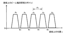
- FIG. 9 shows a schematic example of the beam current density distribution on the substrate 6 stored by the function (a) of the control device 50. This figure for easy understanding of the following description, and the zero current density of the valley portions B 2 together greatly simplifies the distribution waveform.
- the actual beam current density distribution usually has a distribution that smoothly pulsates as in the examples shown in FIGS. 6 and 7, for example.
- the period in the X direction of the beam current density distribution is set to P 2 as described above, and the function of the beam current density distribution is set to f (x).
- x is a position in the X direction on the substrate 6.
- g (t) is a periodic function of time when the amplitude of kP 2/2.
- Trajectory of the point X 0 is the same as the scan waveform shown in FIG. 10.
- Beam current density on the trajectory of the point X 0 is expressed by the following equation. This corresponds to the outline indicated by the bold line in FIG. In FIG. 11, the reason why the beam current density is 0 is because the beam current density distribution shown in FIG. 9 is used in this example, and as described above, the beam current density distribution. If is a different distribution, it will be in accordance with it.
- the ion beam dose W (X 0 , k) for the point X 0 on the substrate 6 during one cycle T S is expressed by the following equation. This integration corresponds to the area of the hatched portion in FIG.
- the coefficient k is changed in predetermined increments to change the scan width kP 2 of the substrate 6, and a plurality of points on the substrate 6 (for example, a plurality of points of 0 ⁇ X 0 ⁇ P 2) for each scan width kP 2 , That is, the ion beam irradiation dose W (X 0 , k) at a plurality of points in the period P 2 is calculated, and its maximum value W (X 0 ′, k) max and minimum value W (X 0 ′′, k) are calculated.
- a difference ⁇ W (refer to the following equation) with respect to min is calculated, and a coefficient k that minimizes the difference ⁇ W is determined, where X 0 ′ is the position of the point where the beam irradiation amount is maximum, and X 0 ′′. Is the position of the point where the beam irradiation amount becomes the minimum value.
- the ion beam irradiation apparatus may further include a beam measuring device that measures the current density distribution of the ion beam 28 in the scanning direction of the substrate 6.
- the beam measuring device may be, for example, a multi-point beam measuring device in which a large number of beam current detectors (for example, a Faraday cup; the same applies hereinafter) are arranged in the scanning direction of the substrate 6, or one beam current detector may be a substrate.
- a movable beam measuring device that moves in the scan direction 6 may be used.
- the beam measuring device 52 shown in FIG. 1 is an example of the former case.
- the beam measuring device may be a movable type that moves to the position of the substrate 6 so as not to interfere with the substrate 6, and is provided at a position upstream or downstream of the substrate 6. Things can be used. 1 shows an example in which the beam measuring device 52 is provided on the downstream side of the substrate 6. When provided on the upstream side of the substrate 6, the substrate 6 may be moved to a position that does not interfere with the irradiation of the ion beam 28 on the substrate 6.
- the control device 50 instead of the function of controlling the scanning width W S of the substrate 6 below the period P 1 of the extraction electrode system 24 as in the embodiment 2 described above Further, based on the current density distribution measured by the beam measuring device, the period P 2 of the current density distribution in the scanning direction of the substrate 6 of the ion beam 28 at the position of the substrate 6 is obtained, and the scan width of the substrate 6 is determined.
- the W S, the calculated period P 2 less (0 is not included) may have a function of controlling the.
- the period P 2 of the beam current density distribution at the position of the substrate 6 is obtained based on the beam current density distribution measured by the beam measuring device, and the obtained period P 2 or less (0 is not included). Since the scan width of the substrate 6 is controlled, the scan width of the substrate 6 can be controlled more accurately. As a result, the same effect as that of the second embodiment can be more reliably achieved. That is, a small scanning width W S, it is possible to improve the uniformity of the beam irradiation amount on the substrate 6. Moreover, since only a small scanning width W S is, it is possible to reduce the size of the ion beam irradiation apparatus. Such an effect can be produced more reliably.
- Embodiment 5 of ion beam irradiation apparatus When the beam measuring instrument as described above is provided, the control device 50 has the following functions (c) and (d) instead of the functions (a) and (b) of the third embodiment described above. You may do it.
- (C) A function for obtaining the current density distribution and its period in the scanning direction of the substrate 6 of the ion beam 28 at the position of the substrate 6 based on the current density distribution measured by the beam measuring device.
- D Assuming that the period of the obtained current density distribution of the ion beam is P 2 and the scan width of the substrate 6 is kP 2 (k is a coefficient of 0 ⁇ k ⁇ 1), the coefficient k is changed in a predetermined step. The scan width kP 2 of the substrate 6 is changed, and the ion beam dose at a plurality of points on the substrate 6 is used for each scan width kP 2 using the obtained current density distribution of the ion beam and the scan waveform of the substrate. Is calculated, the difference between the maximum value and the minimum value is calculated, the coefficient k that minimizes the difference is determined, and the scan width of the substrate 6 is set to kP 2 by using the determined coefficient k. .
- the difference from the functions of (a) and (b) of the third embodiment will be mainly described.
- the function of (c) of this embodiment is based on the beam current density distribution measured by the beam measuring device. The current density distribution of the ion beam at the position 6 and its period are obtained.
- the beam current density distribution and its period at the position of the substrate 6 are obtained based on the beam current density distribution measured by the beam measuring instrument, and the obtained beam current density distribution and its period are used.
- the size of the substrate 6 at the position of the substrate 6 is larger than the size including the substrate 6 and the region where the substrate 6 is scanned.
- the substrate 6 is rotated and scanned in the irradiation region of the ion beam 28 by using an ion beam irradiation apparatus having an ion beam supply unit 18 (for example, the ion source 20) that irradiates the beam 28.
- an ion beam irradiation apparatus having an ion beam supply unit 18 (for example, the ion source 20) that irradiates the beam 28.
- the time required for processing the substrate 6 is shortened and the processing efficiency of the substrate 6 is improved with respect to both scanning and rotation of the substrate 6. be able to.
- the substrate 6 within the irradiation region of the ion beam 28 is scanned with a scan waveform in which the scan position continuously changes with time.
- the method of irradiating the entire surface of the substrate 6 with the ion beam 28 may be employed.
- the size of the substrate 6 at the position of the substrate 6 is larger than the size including the substrate 6 and the region where the substrate 6 is scanned.
- the substrate 6 is placed in the irradiation region of the ion beam 28, and the two types of regions A 1 and B of the extraction electrode system of the ion source 20 are used.
- the substrate 6 is scanned according to a scan waveform in which the scan position changes continuously with time.
- the entire surface of the substrate 6 can be irradiated with an ion beam, and the beam current density distribution on the substrate 6 can be effectively reduced. It is possible to disproportionation. As a result, the uniformity of the beam irradiation amount on the substrate 6 can be further improved.
- an ion beam irradiation apparatus capable of irradiating an entire surface of an substrate with an ion beam and reducing the time required for substrate processing even when the substrate is mechanically scanned and rotated. Can do.
- the ion beam having a size larger than the size including the substrate and the region to be scanned is measured at the position of the substrate.
- An ion beam supply unit that irradiates the substrate, and a rotation mechanism and a scanning mechanism are controlled to rotate and scan the substrate within the ion beam irradiation region, thereby irradiating the entire surface of the substrate with the ion beam.
- the substrate is also rotated in the ion beam irradiation area, and it is not necessary to move the substrate outside the ion beam irradiation area every time the substrate is rotated as in the prior art. Also from this point of view, it is possible to shorten the time required for the substrate processing and improve the substrate processing efficiency.
- the invention according to claim 2 has the following further effects. That is, since the scanning by the scanning mechanism is linear, scanning control is facilitated.
- the ion beam supply unit is an ion source having a plasma generation unit that generates plasma and an extraction electrode system that extracts an ion beam from the plasma by the action of an electric field
- the extraction electrode system includes a substrate and a substrate. Since the ion beam extraction region has a size larger than the size including the region to be scanned, the substrate and the substrate are scanned by spreading a relatively small ion beam extracted from a relatively small ion source. Compared to the case where the substrate is irradiated with an ion beam having a size larger than the size including the region, the current density of the ion beam applied to the substrate can be increased, and thus the processing speed of the substrate can be improved.
- the following further effects are obtained. That is, since the ion beam extraction direction from the ion source is a direction that intersects the direction of gravity, it is not necessary to arrange a substrate directly under the ion source, and foreign matter such as exfoliation pieces of deposits inside the ion source may be generated. Even if it falls from the bottom, it becomes difficult to mix into the substrate. As a result, it is possible to suppress the occurrence of substrate processing defects due to contamination.
- the following further effect is obtained. That is, at least the plasma electrode of the electrode constituting the extraction electrode system of the ion source is provided with a cooling pipe for cooling the electrode, and the plasma electrode has the largest heat input from the plasma generation unit among the electrodes.
- a cooling pipe on at least the plasma electrode, even if the extraction electrode system including the plasma electrode is enlarged, thermal distortion of the plasma electrode can be suppressed. As a result, it is possible to suppress the deterioration of the current density distribution of the ion beam due to the thermal strain of the electrode and the resulting decrease in the uniformity of the substrate processing.
- the region where the ion beam is extracted and the region where the ion beam is not extracted are alternately arranged in a predetermined direction at a predetermined cycle. Therefore, although the ion beam extracted from the ion source has a pulsating current density distribution, this ion beam irradiation apparatus uses the substrate within the irradiation region of the ion beam and the 2 of the extraction electrode system of the ion source. In addition to scanning in a direction parallel to or oblique to the arrangement direction of the types of regions, the substrate is configured to scan according to a scan waveform in which the scan position continuously changes with time. Compared with the prior art, the beam current density distribution on the substrate can be averaged more effectively. As a result, the uniformity of the beam irradiation amount on the substrate can be further improved.
- the scan waveform of the substrate is substantially a triangular wave, the uniformity of the beam irradiation amount on the substrate can be improved with a relatively simple scan waveform.
- the invention according to claim 8 has the following further effect. That is, since the scan waveform of the substrate is substantially a sine wave, the uniformity of the beam irradiation amount on the substrate can be improved with a relatively simple scan waveform. In addition, when the scan waveform is substantially a sine wave, the scan width of the substrate can be made smaller than when the scan waveform is substantially a triangular wave, so that the ion beam irradiation apparatus can be downsized. Become.
- control device further has a function of controlling the scan width of the substrate to be equal to or less than the cycle (not including 0) based on the cycle of the extraction electrode system.
- the uniformity of the beam irradiation amount can be improved.
- the ion beam irradiation apparatus can be downsized.
- control device further has a function of obtaining a scan width that minimizes a difference between the maximum value and the minimum value of the ion beam irradiation amount on the substrate, and setting the scan width of the substrate to the obtained scan width. Therefore, the uniformity of the beam irradiation amount on the substrate can be further improved.
- the invention according to claim 11 has the following further effect. That is, a configuration in which the period of the beam current density distribution at the position of the substrate is obtained based on the beam current density distribution measured by the beam measuring device, and the scan width of the substrate is controlled to be equal to or less than the obtained period (not including 0) Therefore, the scan width of the substrate can be controlled more accurately. As a result, the same effect as the effect of the invention of claim 9 can be achieved more reliably.
- the beam current density distribution at the position of the substrate and the period thereof are obtained based on the beam current density distribution measured by the beam measuring device, and the ion beam on the substrate is obtained using the obtained beam current density distribution and the period. Since the scan width that minimizes the difference between the maximum value and the minimum value of the dose is obtained and the scan width of the substrate is set to the obtained scan width, the beam dose on the substrate is Uniformity can be further improved.
- the ion beam having a size larger than the size of the substrate held by the holder at the position of the substrate is larger than the size including the substrate and the region where the substrate is scanned. Since the substrate is rotated and scanned in the irradiation region of the ion beam using an ion beam irradiation apparatus configured to include an ion beam supply unit that irradiates the ion beam, the entire surface of the substrate is irradiated with the ion beam.
- an ion beam irradiation apparatus configured to include an ion beam supply unit that irradiates the ion beam, the entire surface of the substrate is irradiated with the ion beam.
- the ion beam having a size larger than the size including the substrate and the region to be scanned is measured at the position of the substrate.
- an ion beam irradiation apparatus including an ion source that irradiates the substrate, a substrate is placed in the ion beam irradiation region in parallel or obliquely to the arrangement direction of the two types of regions of the extraction electrode system of the ion source.
- the substrate is scanned in accordance with a scan waveform in which the scan position changes continuously with time, so that the ion is irradiated on the entire surface of the substrate as in the case of the ion beam irradiation apparatus according to claim 6.
- the beam can be irradiated and the beam current density distribution on the substrate can be effectively averaged. As a result, the uniformity of the beam irradiation amount on the substrate can be further improved.
Landscapes
- Chemical & Material Sciences (AREA)
- Analytical Chemistry (AREA)
- Physics & Mathematics (AREA)
- Engineering & Computer Science (AREA)
- Plasma & Fusion (AREA)
- Physical Vapour Deposition (AREA)
Abstract
本発明は、基板の全面にイオンビームを照射することができ、しかも基板をスキャンおよび回転させても基板処理に要する時間を短縮することを目的としており、このイオンビーム照射装置は、真空容器(4)内に収納されたホルダ(8)およびそれに保持された基板(6)をその中心部周りに回転させる回転機構(10)と、ホルダ(8)、基板(6)および回転機構(10)を機械的にスキャンするスキャン機構(14)とを備えている。更に、ホルダ(8)上の基板(6)に対して、基板(6)の位置における寸法が、基板(6)および基板(6)がスキャンされる領域を包含する大きさよりも大きい寸法のイオンビーム(28)を照射するイオンビーム供給部(18)と、回転機構(10)およびスキャン機構(14)を制御して、イオンビーム(28)の照射領域内で基板(6)を回転およびスキャンさせて、基板(6)の全面にイオンビーム(28)を照射する機能を有している制御装置(50)とを備えている。
Description
この発明は、例えばイオンミリング装置、イオン注入装置等のように、真空雰囲気中で基板にイオンビームを照射することによって基板に処理を施すイオンビーム照射装置およびイオンビーム照射方法に関する。
長辺の寸法が基板よりも大きく短辺の寸法が基板よりも小さい断面長方形のイオンビームを引き出すイオン源と、基板が上記イオンビームの照射領域の内外に位置するように、基板をイオンビームの短辺方向に並進させる並進機構と、基板がイオンビームの照射領域外にある時に基板をその中心部周りに回転させる回転機構とを備えていて、基板の全面にイオンビームを照射して基板に処理を施す処理装置および処理方法が、例えば特許文献1に記載されている。
上記従来の技術においては、基板の並進毎に、基板をイオンビームの照射領域外に移動させるので、基板の処理効率が低下し、基板処理に要する時間が長くなるという課題がある。
また、基板をイオンビームの照射領域外で回転させるために、基板を回転させる度に基板をイオンビームの照射領域外へ移動(並進)させる必要があり、それによって並進回数が多くなるので、この観点からも、基板処理に要する時間が長くなるという課題がある。基板を少しずつ幾度もステップ回転させる場合は、特に基板処理に要する時間が長くなる。
そこでこの発明は、基板の全面にイオンビームを照射することができ、しかも基板を機械的にスキャンおよび回転させても基板処理に要する時間を短縮することができるイオンビーム照射装置を提供することを一つの目的としている。
また、上記のような処理を行うことができるイオンビーム照射方法を提供することを他の目的としている。
この発明に係るイオンビーム照射装置は、真空雰囲気中で基板にイオンビームを照射する装置であって、真空に排気される真空容器と、前記真空容器内に収納されていて基板を保持するホルダと、前記ホルダおよびそれに保持された基板を当該基板の中心部周りに回転させる回転機構と、前記ホルダ、それに保持された基板および前記回転機構を機械的に往復でスキャンするスキャン機構と、前記ホルダに保持された基板に対して、当該基板の位置における寸法が、当該基板および当該基板がスキャンされる領域を包含する大きさよりも大きい寸法のイオンビームを照射するイオンビーム供給部と、前記回転機構および前記スキャン機構を制御して、前記イオンビームの照射領域内で前記基板を回転およびスキャンさせて、前記基板の全面にイオンビームを照射する機能を有している制御装置とを備えている、ことを特徴としている。
このイオンビーム照射装置は、前記ホルダに保持された基板に対して、当該基板の位置における寸法が、当該基板および当該基板がスキャンされる領域を包含する大きさよりも大きい寸法のイオンビームを照射するイオンビーム供給部と、前記回転機構および前記スキャン機構を制御して、前記イオンビームの照射領域内で前記基板を回転およびスキャンさせて、前記基板の全面にイオンビームを照射する機能を有している制御装置とを備えていて、イオンビームの照射領域内で基板をスキャンする構成であり、前記従来技術のように基板のスキャン毎に基板をイオンビームの照射領域外に移動させる必要はないので、基板処理に要する時間を短縮して基板の処理効率を向上させることができる。
また、基板の回転に関しても、イオンビームの照射領域内で基板を回転させる構成であり、前記従来技術のように基板を回転させる度に基板をイオンビームの照射領域外へ移動させる必要はないので、この観点からも、基板処理に要する時間を短縮して基板の処理効率を向上させることができる。
前記イオンビーム供給部は、プラズマを生成するプラズマ生成部および当該プラズマから電界の作用でイオンビームを引き出す引出し電極系を有しているイオン源であり、しかも当該引出し電極系は、前記基板および前記基板がスキャンされる領域を包含する大きさよりも大きい寸法のイオンビーム引出し領域を有している、という構成を採用しても良い。また、その他の変形例を採用しても良い。
前記イオンビーム供給部は、プラズマを生成するプラズマ生成部と、前記プラズマから電界の作用でイオンビームを引き出す引出し電極系を備え、前記引出し電極系には、前記イオンビームが引き出される領域と引出されない領域が、所定周期で配列されていて、前記スキャン機構によるスキャンの方向は、前記引出電極系の前記2種類の領域の配列方向に対して平行または斜めであり、更に、前記制御装置は、スキャン位置が時間によって連続的に変化するスキャン波形に従って、前記スキャン機構を制御する、という構成を採用しても良い。
前記制御装置は、前記基板のスキャン幅を、引出し電極系の前記周期に基づいて当該周期以下(0を含まない)に制御する機能を更に有していても良い。
前記制御装置は、基板上におけるイオンビーム照射量の最大値と最小値との差を最小とするスキャン幅を求めて、前記基板のスキャン幅を当該求めたスキャン幅にする機能を更に有していても良い。
前記基板のスキャン方向におけるイオンビームの電流密度分布を測定するビーム測定器を設けて、当該ビーム測定器で測定した電流密度分布を、前記基板のスキャン幅の制御に用いても良い。
この発明に係るイオンビーム照射方法は、真空雰囲気中で基板にイオンビームを照射する方法であって、真空に排気される真空容器と、前記真空容器内に収納されていて基板を保持するホルダと、前記ホルダおよびそれに保持された基板を当該基板の中心部周りに回転させる回転機構と、前記ホルダ、それに保持された基板および前記回転機構を機械的に往復でスキャンするスキャン機構と、前記ホルダに保持された基板に対して、当該基板の位置における寸法が、当該基板および当該基板がスキャンされる領域を包含する大きさよりも大きい寸法のイオンビームを照射するイオンビーム供給部とを備えている構成のイオンビーム照射装置を用いて、前記イオンビームの照射領域内で前記基板を回転およびスキャンさせて、前記基板の全面にイオンビームを照射することを特徴としている。
この発明に係るイオンビーム照射方法は、真空雰囲気中で基板にイオンビームを照射する方法であって、真空に排気される真空容器と、前記真空容器内に収納されていて基板を保持するホルダと、プラズマを生成するプラズマ生成部および当該プラズマから電界の作用でイオンビームを引き出す引出し電極系を有していて、引き出したイオンビームを前記ホルダに保持された基板に照射するイオン源であって、前記引出し電極系は、イオンビームが引き出される領域とイオンビームが引き出されない領域とを所定の方向に所定の周期で交互に配列しているイオン源と、前記ホルダおよびそれに保持された基板を、前記引出し電極系の前記2種類の領域の配列方向に対して平行または斜めの方向に機械的に往復でスキャンするスキャン機構とを備えており、かつ前記イオン源は、前記ホルダに保持された基板に対して、当該基板の位置における寸法が、当該基板および当該基板がスキャンされる領域を包含する大きさよりも大きい寸法のイオンビームを照射するものである、という構成のイオンビーム照射装置を用いて、前記イオンビームの照射領域内で前記基板を、スキャン位置が時間によって連続的に変化するスキャン波形に従ってスキャンして、前記基板の全面にイオンビームを照射することを特徴としている。
本発明によれば、基板の全面にイオンビームを照射することができ、しかも基板を機械的にスキャンおよび回転させても基板処理に要する時間を短縮することができる。
4・・・真空容器
6・・・基板
8・・・ホルダ
10・・・回転機構
14・・・スキャン機構
18・・・イオンビーム供給部
20・・・イオン源
22・・・プラズマ生成部
23・・・プラズマ
24・・・引出し電極系
26・・・イオンビーム引出し領域
28・・・イオンビーム
31・・・プラズマ電極
32・・・引出し電極
33・・・接地電極
40、41・・・冷却パイプ
50・・・制御装置
52・・・ビーム測定器
A1・・・イオンビームが引き出される領域
B1・・・イオンビームが引き出されない領域
6・・・基板
8・・・ホルダ
10・・・回転機構
14・・・スキャン機構
18・・・イオンビーム供給部
20・・・イオン源
22・・・プラズマ生成部
23・・・プラズマ
24・・・引出し電極系
26・・・イオンビーム引出し領域
28・・・イオンビーム
31・・・プラズマ電極
32・・・引出し電極
33・・・接地電極
40、41・・・冷却パイプ
50・・・制御装置
52・・・ビーム測定器
A1・・・イオンビームが引き出される領域
B1・・・イオンビームが引き出されない領域
(1)イオンビーム照射装置の実施形態1
図1に、この発明に係るイオンビーム照射装置の一実施形態を示す。方向の理解を容易にするために、各図中に、1点で互いに直交するX方向、Y方向およびZ方向を図示している。例えば、Y方向およびZ方向は水平方向であり、X方向は垂直方向である。イオンビーム28は、この例ではZ方向に進行する。
図1に、この発明に係るイオンビーム照射装置の一実施形態を示す。方向の理解を容易にするために、各図中に、1点で互いに直交するX方向、Y方向およびZ方向を図示している。例えば、Y方向およびZ方向は水平方向であり、X方向は垂直方向である。イオンビーム28は、この例ではZ方向に進行する。
このイオンビーム照射装置は、真空雰囲気中で基板6にイオンビーム28を照射する装置であって、図示しない真空排気装置によって真空に排気される真空容器4と、この真空容器4内に収納されていて処理しようとする基板6を保持するホルダ8と、このホルダ8およびそれに保持された基板6を当該基板6の中心部6a周りに回転させる回転機構10とを備えている。その回転方向Cの一例を図中に示すが、これと逆方向でも良い。また、回転機構10によるホルダ8および基板6の回転は、連続回転でも良いし、所定の角度ごとのステップ回転でも良い。
基板6は、例えばシリコンウェーハ等の半導体基板、半導体基板の表面に磁性体膜等の膜が形成された基板等であるが、これに限られるものではない。
基板6の形状は、例えば円形(円周の一部分にオリエンテーションフラットやノッチを有するものもこれに含むものとする)であるが、これに限られるものではない。
このイオンビーム照射装置は、更に、ホルダ8、それに保持された基板6等を傾けて、イオンビーム28に対する基板6のチルト角(傾き角)φを変更するチルト機構12を備えている。このチルト機構12によるチルト角φの変更は、イオンビーム28の照射領域内で行っても良いし、照射領域外で行っても良い。但し、このチルト機構12は本発明に必須のものではない。
このイオンビーム照射装置は、更に、プラズマ23を生成するプラズマ生成部22および当該プラズマ23から電界の作用でイオンビーム28を引き出す引出し電極系24を有していて、引き出したイオンビーム28をホルダ8に保持された基板6に照射するイオン源20を備えている。イオン源20は、その引出し電極系24と共に、真空容器4の内部に配置しても良いし、真空容器4の外部に配置しても良い。引出し電極系24は、例えば図4、図5に示す例のように、イオンビーム28が引き出される領域A1とイオンビーム28が引き出されない領域B1とを所定の方向(この実施形態ではX方向)に所定の周期P1で交互に配列した構成を有している。この引出し電極系24については後で更に説明する。
このイオンビーム照射装置は、更に、軸16を介して、ホルダ8、それに保持された基板6、回転機構10およびチルト機構12を機械的に往復でスキャン(即ち、機械的往復走査)するスキャン機構14を備えている。このスキャン機構14による上記スキャンは、例えば直線状である。その場合のスキャン方向Dの一例を図中に示している。スキャン機構14は、この例では真空容器4外に設けているが、これに限られるものではない。
スキャン機構14によるホルダ8、基板6等のスキャン方向Dは、この実施形態では引出し電極系24の前記2種類の領域A1、B1の配列方向(X方向)に平行な方向であるが、引出し電極系24の上記2種類の領域A1、B1の配列方向に対して斜めの方向でも良い。
イオン源20は、ホルダ8に保持された基板6に対して、図2に示す例のように、当該基板6の位置における寸法が、基板6および当該基板6がスキャンされる領域を包含する大きさよりも大きい寸法のイオンビーム28を照射するものである。図2中に、基板6のスキャン方向Dおよびスキャン幅WSの例も示している。即ち、図2中に破線で示す基板6はスキャンの一方端に位置し、2点鎖線で示す基板6はスキャンの他方端に位置している場合の例を示している。
イオン源20の種類は特定のものに限定されない。例えば、イオン源20は、(a)多極磁界(カスプ磁界)を用いてプラズマ23の閉じ込め等を行う、いわゆるバケット型イオン源(多極磁界型イオン源とも呼ばれる)でも良いし、(b)高周波放電によってプラズマ23を生成する高周波イオン源でも良いし、(c)陰極と反射電極とを対向させ、かつ両者を結ぶ軸に沿う方向に磁界を印加してプラズマ23を生成する、いわゆるバーナス型イオン源でも良い。引出し電極系24を構成する電極の数も、特定のものに限定されない。
上記(a)のバケット型イオン源の場合は、例えば、大面積で均一性の良いプラズマ23を生成して、大面積で均一性の良いイオンビーム28の引き出しが容易になるという利点を有している。上記(b)の高周波イオン源は、例えば、引出し電極系24を構成する電極への熱入力が小さいという利点を有している。
なお、イオン源20からのイオンビーム28の引き出し方向は、重力方向Gと交差する方向(例えば、図1に示す例のように実質的に直交する方向、または斜めの方向)にするのが好ましい。そのようにすると、イオン源20の真下に基板6を配置せずに済み、イオン源20内部の堆積物の剥離片等の異物(ゴミ)がイオン源20から落下しても基板6に混入しにくくなる。その結果、異物混入による基板6の処理不良の発生を抑制することができる。
図1に示す例のイオン源20のより詳細例を、図3等を参照して更に説明する。プラズマ23を生成するプラズマ生成部22は、例えば、前述したバケット型イオン源、高周波イオン源、バーナス型イオン源等を構成する公知のプラズマ生成部であり、図3では簡略化して図示している。
図3に示す例のイオン源20は、上記引出し電極系24を構成するものとして複数枚(この例では3枚)の電極31~33を有している。この出願では、当該3枚の電極の内、最もプラズマ23側の電極をプラズマ電極31と呼び、その下流側(イオンビーム28の進行方向における下流側。以下同様)の電極を引出し電極32と呼び、その下流側の電極を接地電極33と呼ぶ。例えば、プラズマ電極31には、図示しない直流電源から、正の加速電圧が印加される。引出し電極32には、図示しない直流電源から、プラズマ電極31の電位よりも低い正の引出し電圧が印加される。接地電極33は電気的に接地される。
引出し電極系24は、より具体的にはその各電極31~33は、この実施形態では、基板6および当該基板6がスキャンされる領域を包含する大きさよりも大きい寸法のイオンビーム引出し領域26(図4、図5参照)を有している。イオンビーム引出し領域26は、イオンビーム28を引き出す孔、スリット等の多数の開口(イオン引出し開口)を有している領域である。例えば、図4に示すイオンビーム引出し領域26は、多数の孔34を有しており、図5に示すイオンビーム引出し領域26は、多数のスリット37を有している。寸法の一例を挙げると、基板6の直径が300mm、そのスキャン幅WSが80mmの場合、イオンビーム引出し領域26の縦横の寸法は400mm×400mmである。但しこれに限られるものではない。
上記3枚の電極31~33は、この例では、冷却パイプ40、41の部分を除いて、ほぼ同様の構成をしているので、プラズマ電極31で代表して、そのイオンビーム引出し領域26部分の平面図を図4または図5に示している。
各電極31~33は、図3、図4に示す例のように、イオンビーム28引き出し用の多数の孔34を有していても良いし、図5に示す例のように、イオンビーム28引き出し用の多数のスリット37を有していても良い。
引出し電極系24を構成する電極に、例えば少なくともプラズマ電極31に、当該電極を冷却する冷却パイプを設けておいても良い。この例では、プラズマ電極31に複数の冷却パイプ40をX方向に一定のピッチで配置している。冷却パイプ40内には、例えば冷却水等の冷媒が流される。冷却パイプ40を設けた部分からイオンビーム28は引き出されないので、図4、図5に示す例のように、引出し電極系24は、複数の孔34(図4参照)または複数のスリット37(図5参照)を有していてイオンビーム28が引き出される領域A1と、冷却パイプ40が設けられていてイオンビーム28が引き出されない領域B1とが、所定方向(この例ではX方向)に所定の周期P1で交互に配列された構造を有している。
プラズマ電極31よりも下流側の電極にも、必要に応じて、当該電極を冷却する冷却パイプを設けても良い。図3に示す例では、引出し電極32にも複数の冷却パイプ41を設けている。各冷却パイプ41は、この例では各冷却パイプ40の位置に対応させて配置している。冷却パイプ41内には、例えば冷却水等の冷媒が流される。
上記のような2種類の領域A1、B1を有する引出し電極系24を備えているイオン源20から引き出されるイオンビーム28の、基板6の位置における電流密度分布の一例を図6に示す。この電流密度分布は、一定の周期P2で脈動している。山部分A2は引出し電極系24のイオンビームが引き出される領域A1に対応する部分であり、谷部分B2は引出し電極系24のイオンビームが引き出されない領域B1に対応する部分である。この周期P2と引出し電極系24の上記周期P1との関係は、特別な場合(例えばイオンビーム28の発散が大きい場合)を除いて、P1≒P2と考えることができる場合が多い。
上記図6に示す電流密度分布はほんの一例であり、引出し電極系24の上記二つの領域A1、B1の幅の大小関係や、各領域A1の各孔やスリットから引き出されるイオンビームの発散角の大小等によって、より脈動の小さい電流密度分布、より脈動の大きい電流密度分布、更にはその他の電流密度分布を実現することもできる。例えば後述する図7参照。
プラズマ電極31はプラズマ生成部22からの熱入力が最も大きいので、それの冷却能力をより高めるために、上記各イオンビームが引き出される領域A1の中間部に、冷却パイプ40と平行に、冷却パイプ40よりも細い冷却パイプを更に配置しても良い。そのようにしても、大きくとらえた上記領域A1の基本となる周期は依然としてP1であると言うことができる。また、上記の付加的な冷却パイプを配置すると、当該冷却パイプ部分からイオンビームが引き出されなくなるので、イオンビーム28の電流密度分布の各山部分、例えば図6に示した電流密度分布の各山部分A2が二山になるけれども、ビーム電流密度分布の基本となる(即ち大きくとらえた)周期は依然としてP2であると言うことができる。
イオン源20の引出し電極系24は、それを構成する電極の内の少なくとも1枚に、分割構造の電極を有していても良い。ここで言う分割構造の電極は、多数のイオン引出し開口(例えば前記孔34またはスリット37に相当する開口)をそれぞれ有している複数枚の電極片を、所定の方向(例えば図4等に示すY方向)に伸びる接続部を有していて、所定の方向(例えばX方向)に所定の周期で並べて接続して1枚の電極を構成したものである。各接続部はイオン引出し開口を有していないので、当該接続部からイオンビームは引き出されない。従って引出し電極系24がこのような分割構造の電極を有している場合も、当該引出し電極系24は、イオンビーム28が引き出される領域(上記領域A1に相当)とイオンビーム28が引き出されない領域(上記領域B1に相当)とが所定の方向に所定の周期(上記周期P1に相当)で交互に配列された構造を有している。
再び図1を参照して、このイオンビーム照射装置は、更に、上記回転機構10およびスキャン機構14を制御して、上記イオンビーム28の照射領域内で基板6を回転およびスキャンさせて、基板6の全面にイオンビーム28を照射する機能を有している制御装置50を備えている。上記チルト機構12を備えている場合は、制御装置50は、当該チルト機構12を制御して上記チルト角φを制御する機能を更に有していても良い。
このイオンビーム照射装置によれば、基板6の全面にイオンビーム28を照射して、当該基板6に処理を施すことができる。例えば、基板6にその表面を削る等のイオンミリング加工を施すことができる。また、基板6にイオン注入を行うこともできる。イオンビーム28の種類は、基板6に施す処理内容に応じて選定すれば良い。例えば、イオンミリングを行う場合は、イオンビーム28として、例えばアルゴンイオンビームのような不活性ガスイオンビーム等を用いれば良い。イオン注入を行う場合は、イオンビーム28として、所望のドーパントを含むイオンビームを用いれば良い。
しかもこのイオンビーム照射装置は、ホルダ8に保持された基板6に対して、基板6の位置における寸法が、基板6および当該基板6がスキャンされる領域を包含する大きさよりも大きい寸法のイオンビーム28を照射するイオンビーム供給部18と、回転機構10およびスキャン機構14を制御して、前記イオンビーム28の照射領域内で基板6を回転およびスキャンさせて、基板6の全面にイオンビーム28を照射する機能を有している制御装置50とを備えていて、イオンビーム28の照射領域内で基板6をスキャンする構成であり、前記従来技術のように基板のスキャン毎に基板をイオンビームの照射領域外に移動させる必要はないので、基板6の処理に要する時間を短縮して基板6の処理効率を向上させることができる。
また、基板6の回転に関しても、イオンビーム28の照射領域内で基板6を回転させる構成であり、前記従来技術のように基板を回転させる度に基板をイオンビームの照射領域外へ移動させる必要はないので、この観点からも、基板6の処理に要する時間を短縮して基板6の処理効率を向上させることができる。
スキャン機構14による基板6等の上記スキャンは、この実施形態のように直線状でも良いし、直線状以外でも良い。直線状にすれば、スキャンの制御が容易になる。直線状以外では、例えば、特開平3-74040号公報等に記載されているように、基板を保持するホルダをアームの一端部で支持し、当該アームの他端部に可逆転式の回転駆動源を連結して、当該アーム(スイングアームとも呼ばれる)を所定角度範囲内において往復で旋回させる(スイングさせる)方式によって基板6等をスキャンしても良い。
また、本実施形態の制御装置50は、更に、前記スキャン機構14を制御して、前記イオンビーム28の照射領域内で基板6を、スキャン位置が時間によって連続的に変化するスキャン波形に従ってスキャンして、基板6の全面にイオンビーム28を照射する機能を有している。
スキャン位置が時間によって連続的に変化するスキャン波形は、換言すればスキャン中にスキャンが停止する部分を含まない波形であり、例えば、三角波、三角波が幾分鈍化している鈍化三角波、正弦波、正弦波が幾分歪んでいる歪み正弦波等である。台形波は、波形が平坦になってスキャン中にスキャンが停止する時間帯を含んでいるので、ここで言うスキャン波形には含まない。
このイオンビーム照射装置によれば、ホルダ8に保持された基板6に対して、当該基板6の位置における寸法が、基板6および当該基板6がスキャンされる領域を包含する大きさよりも大きい寸法のイオンビーム28を照射するイオン源20を備えているので、基板6の全面にイオンビーム28を照射して、当該基板6に処理を施すことができる。
例えば、基板6にその表面を削る等のイオンミリング加工を施すことができる。また、基板6にイオン注入を行うこともできる。イオンビーム28の種類は、基板6に施す処理内容に応じて選定すれば良い。例えば、イオンミリングを行う場合は、イオンビーム28として、例えばアルゴンイオンビームのような不活性ガスイオンビーム等を用いれば良い。イオン注入を行う場合は、イオンビーム28として、所望のドーパントを含むイオンビームを用いれば良い。
また、上記イオン源20の引出し電極系24は、イオンビーム28が引き出される領域A1とイオンビームが引き出されない領域B1とを所定の方向に所定の周期P1で交互に配列した構成を有しているので、当該イオン源20から引き出されるイオンビーム28は脈動する電流密度分布を有することになるけれども、このイオンビーム照射装置は、当該イオンビーム28の照射領域内で基板6を、イオン源20の引出し電極系24の前記2種類の領域A1、B1の配列方向に対して平行または斜めの方向にスキャンすることに加えて、当該基板6を、スキャン位置が時間によって連続的に変化するスキャン波形に従ってスキャンする構成(スキャン機構14および制御装置50)を有していて、当該スキャンによって、基板6上におけるイオンビーム28の脈動する電流密度分布によるビーム濃淡の影響をうまく解消することができるので、前記従来技術の場合に比べて基板6上におけるビーム電流密度分布をより効果的に平均化することができる。その結果、基板6上でのビーム照射量の均一性を更に向上させることができる。
なお、基板6等のスキャン方向Dは、上記2種類の領域A1、B1の配列方向に平行な方向が好ましいけれども、当該配列方向に対して斜めの方向でも良く、その場合でも上記とほぼ同様の作用によって、上記基板6上におけるビーム濃淡の影響を解消する効果を奏することができる。スキャン方向Dを上記のように斜めの方向にする場合は、引出し電極系24の上記2種類の領域A1、B1の配列の周期P1および基板6上でのビーム電流密度分布の周期P2は、当該斜めの方向の周期を用いれば良い。以下に述べる他の実施形態においても同様である。
また、スキャン位置が時間によって連続的に変化する上記スキャン波形は、前述した台形波のようにスキャン波形中にスキャンが停止する時間帯を含んでいるスキャン波形に比べて、スキャン波形が単純であるので、制御装置50によるスキャン制御が容易になるという利点もある。
ちなみに、前述した台形波のように、スキャン波形中にスキャンが停止する時間帯を含んでいるスキャン波形の場合は、基板6上に、イオンビーム28の脈動する電流密度分布によるビーム濃淡の影響が色濃く残り、しかもこの影響は基板6の停止時間が長くなるほど大きくなるので、基板6上でのビーム照射量の均一性を向上させることが困難になる。従ってこのようなスキャン波形は好ましくない。
次に、基板6のスキャン波形およびスキャン幅WSの例について説明する。
上記基板6のスキャン波形は、実質的に三角波としても良い。実質的に三角波とは、三角波、および三角波が幾分鈍っている鈍化三角波を含む意味である。このようなスキャン波形を用いれば、比較的単純なスキャン波形で基板6上でのビーム照射量の均一性を向上させることができる。鈍化三角波については、以下において更に詳しく説明する。
あるいは基板6のスキャン波形は、実質的に正弦波としても良い。実質的に正弦波とは、正弦波、および正弦波が幾分歪んでいる歪み正弦波を含む意味である。このようなスキャン波形を用いれば、比較的単純なスキャン波形で基板6上でのビーム照射量の均一性を向上させることができる。しかもスキャン波形が実質的に正弦波の場合は、実質的に三角波の場合に比べて基板6のスキャン幅WSを小さくすることが可能になるので、当該イオンビーム照射装置の小型化を図ることが可能になる。このスキャン幅WSを小さくすることが可能になることについては、以下において更に詳しく説明する。
基板6のスキャン波形が三角波、鈍化三角波および正弦波の場合について、基板6上でのビーム照射量の均一性についてシミュレーションを行った結果の例を説明する。
イオンビーム28の分布としては、ここでは、図7に示す例のように、基板6上におけるビーム電流密度分布の各山部分(図6中の各山部分A2に対応)がガウス分布をしていて、そのピーク強度が1/eとなる幅(これを1/e幅と呼ぶことにする。eは自然対数の底であり、e≒2.718である)が異なる場合について検討した。
(A)イオンビームの分布
基板6上のスキャン方向(この例ではX方向)における各山部分の電流密度分布I(x)は、次式で表されるガウス分布であるとする。ここで、xは基板6上のX方向の位置、I0はピーク強度、dは上記1/e幅である。
基板6上のスキャン方向(この例ではX方向)における各山部分の電流密度分布I(x)は、次式で表されるガウス分布であるとする。ここで、xは基板6上のX方向の位置、I0はピーク強度、dは上記1/e幅である。

なお、以下では、計算を単純化する等のために、上記式のビーム電流密度分布をI0で規格化した(即ちI0=1とした)規格化ビーム電流密度分布を用いる。図7はそれを用いて図示している。
基板6上のスキャン方向におけるビーム電流密度分布の周期をP2とし、距離の単位をP2/2とする。図7に示すビーム電流密度分布は、基板6上における山部分が五つで、上記距離の単位での各中心がx=-4,-2,0,2,4にそれぞれある場合の例である。
各山部分の1/e幅(=d)は、d=1/3,2/3,1の3条件でシミュレーションを行った。
上記五つの山部分を有するイオンビーム全体の基板6上でのビーム電流密度分布f(x)は次式で表すことができる。

上記数2で表されるビーム電流密度分布f(x)を、上記各1/e幅についてグラフ化したものを図7にまとめて示している。
(B)基板6のスキャン波形
基板6のスキャン波形として、ここでは三角波を取り上げ、それをフーリエ級数で表すことにするが、無限フーリエ級数を用いるのは実用的ではなく、有限フーリエ級数でも項数をある程度大きくすれば無限フーリエ級数と実質的に同じとみなせるので、ここでは次式に示すように有限項(33項)のフーリエ級数f(t)で三角波を表すことにした。nは1以上の整数であり、ここでは1から33までの整数である。
基板6のスキャン波形として、ここでは三角波を取り上げ、それをフーリエ級数で表すことにするが、無限フーリエ級数を用いるのは実用的ではなく、有限フーリエ級数でも項数をある程度大きくすれば無限フーリエ級数と実質的に同じとみなせるので、ここでは次式に示すように有限項(33項)のフーリエ級数f(t)で三角波を表すことにした。nは1以上の整数であり、ここでは1から33までの整数である。

また、前述した三角波が鈍化した鈍化三角波には、上記数3におけるn=33の代わりに、n=9,5,3をそれぞれ使用した。これらの鈍化三角波の振幅は、波形の頂部が鈍化しているために、三角波の振幅よりも幾分小さくなる。三角波の振幅を1としたとき、上記n=9,5,3の場合の鈍化三角波の振幅は、それぞれ、0.96(96%)、0.93(93%)、0.90(90%)になる。この割合を鈍化率と呼ぶことにし、これらの鈍化三角波を、それぞれ、鈍化三角波1、鈍化三角波2、鈍化三角波3と呼ぶことにする。なお、鈍化率は、三角波を有限項のフーリエ級数で表したときの振幅の、無限項のフーリエ級数で表したときの振幅に対する割合と言うこともできる。
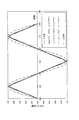
上記三角波、鈍化三角波1~3およびこれらと同じ周期の正弦波から成るスキャン波形の例を図8にまとめて示す。
(C)基板6のスキャン波形、スキャン幅およびビーム電流密度分布の均一性
基板6上におけるビーム電流密度分布が図7を参照して説明した3種類の場合について、基板6上の上記5種類のスキャン波形について、基板6のスキャン幅WSおよびその時の基板6上でのビーム照射量の均一性Uを求めた結果を表1にまとめて示す。
基板6上におけるビーム電流密度分布が図7を参照して説明した3種類の場合について、基板6上の上記5種類のスキャン波形について、基板6のスキャン幅WSおよびその時の基板6上でのビーム照射量の均一性Uを求めた結果を表1にまとめて示す。
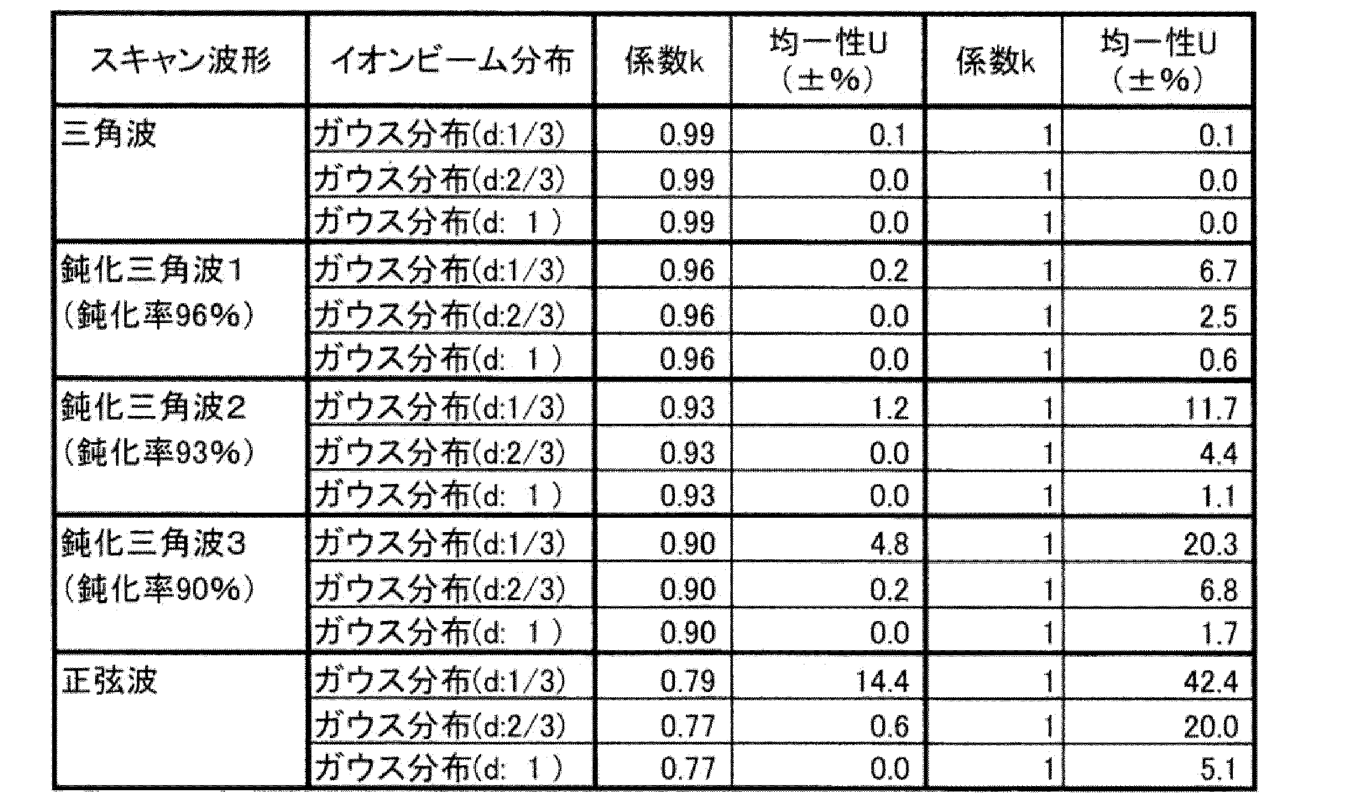
ここでは、基板6のスキャン幅WSは、前述した基板6上のスキャン方向におけるビーム電流密度分布の周期P2に対する比率を表す係数k(>0)を用いて、次式の関係で表しており、表1中にはこの係数kを記入している。

また、基板6上でのビーム照射量の均一性Uは、次式で表されるものである。ここで、Wmaxはビーム照射量の最大値、Wminはビーム照射量の最小値である。

上記表1から分るように、どのスキャン波形の場合も、係数kを1以下(0を含まない)にすることで良好な均一性Uが得られている。
特に、スキャン波形が三角波の場合は、係数kが1または0.99で非常に良好な均一性Uが得られており、これが最適なスキャン幅WSを与える係数であると言うことができる。
スキャン波形が鈍化三角波の場合は、係数kを上記鈍化率と同じ値にすることで、非常に良好な均一性Uが得られており、これが最適なスキャン幅WSを与える係数であると言うことができる。
スキャン波形が正弦波の場合は、係数kが0.77~0.79で非常に良好な均一性Uが得られており、これが最適なスキャン幅WSを与える係数であると言うことができる。即ち、スキャン波形が正弦波の場合は、三角波や鈍化三角波に比べて、基板6のスキャン幅WSを小さくすることが可能になる。
なお、表1に示すように、スキャン波形が鈍化三角波でも良好な均一性Uが得られることから、スキャン波形が、正弦波が幾分(例えば数%以下)歪んでいる歪み正弦波の場合も、上記正弦波の場合の係数k程度の係数kで良好な均一性Uが得られるものと考えられる。
次に、制御装置50が他の機能を有している等の場合のイオンビーム照射装置の他の実施形態について幾つか説明する。以下においては、上述した実施形態との相違点を主に説明する。
(2)イオンビーム照射装置の実施形態2
図6の所で説明したように、引出し電極系24の2種類の領域A1、B1の周期P1と、基板6上でのビーム電流密度分布の周期P2とは、特別な場合を除いて、P1≒P2と考えることができる場合が多いので、上記周期P2を用いる代わりに上記周期P1を用いて、上記係数kを周期P1に掛けてスキャン幅WSを決定しても良い。即ちWS=kP1(kは0<k≦1)としても良い。引出し電極系24の上記周期P1は引出し電極系24の構造から容易に分かるので、この周期P1を用いる方が簡単である。
図6の所で説明したように、引出し電極系24の2種類の領域A1、B1の周期P1と、基板6上でのビーム電流密度分布の周期P2とは、特別な場合を除いて、P1≒P2と考えることができる場合が多いので、上記周期P2を用いる代わりに上記周期P1を用いて、上記係数kを周期P1に掛けてスキャン幅WSを決定しても良い。即ちWS=kP1(kは0<k≦1)としても良い。引出し電極系24の上記周期P1は引出し電極系24の構造から容易に分かるので、この周期P1を用いる方が簡単である。
即ち、前記制御装置50は、基板6のスキャン幅WSを、引出し電極系24の前記周期P1に基づいて当該周期P1以下(0を含まない)に制御する機能を更に有していても良い。そのようにすると、小さいスキャン幅WSで、基板6上でのビーム照射量の均一性を向上させることができる。また、スキャン幅WSが小さくて済むので、当該イオンビーム照射装置の小型化を図ることができる。逆に、基板6のスキャン幅WSを引出し電極系24の上記周期P1よりも大きくすると、スキャン幅WSが大きくなった分、当該イオンビーム照射装置が大型になる。
(3)イオンビーム照射装置の実施形態3
制御装置50が、上記実施形態2で説明したように、基板6のスキャン幅WSを引出し電極系24の上記周期P1以下(0を含まない)に制御する機能を有している場合、制御装置50は、次の(a)および(b)の機能を更に有していても良い。
制御装置50が、上記実施形態2で説明したように、基板6のスキャン幅WSを引出し電極系24の上記周期P1以下(0を含まない)に制御する機能を有している場合、制御装置50は、次の(a)および(b)の機能を更に有していても良い。
(a)基板6の位置でのイオンビーム28の、基板6のスキャン方向における電流密度分布であってスキャン機構14の制御に用いるものを記憶しておく機能。
(b)前記記憶しているイオンビームの電流密度分布の周期をP2、基板6のスキャン幅をkP2(kは0<k≦1の係数)とすると、係数kを所定の刻みで変化させて基板6のスキャン幅kP2を変化させ、各スキャン幅kP2ごとに、前記記憶しているイオンビームの電流密度分布および前記基板のスキャン波形を用いて、基板6上の複数点におけるイオンビームの照射量を計算してその最大値と最小値との差を計算し、かつ当該差を最小とする係数kを決定し、当該決定した係数kを用いて、基板6のスキャン幅をkP2とする機能。
(b)前記記憶しているイオンビームの電流密度分布の周期をP2、基板6のスキャン幅をkP2(kは0<k≦1の係数)とすると、係数kを所定の刻みで変化させて基板6のスキャン幅kP2を変化させ、各スキャン幅kP2ごとに、前記記憶しているイオンビームの電流密度分布および前記基板のスキャン波形を用いて、基板6上の複数点におけるイオンビームの照射量を計算してその最大値と最小値との差を計算し、かつ当該差を最小とする係数kを決定し、当該決定した係数kを用いて、基板6のスキャン幅をkP2とする機能。
これについて更に説明すると、制御装置50の上記(a)の機能で記憶しておく基板6上でのビーム電流密度分布は、例えば、本イオンビーム照射装置と同等のイオンビーム照射装置を用いる等して、予め実験的に上記ビーム電流密度分布を測定して、それを記憶しておけば良い。また、イオンビーム28のエネルギー、電流値、イオン種等の各種条件(これはレシピと呼ばれる)を変化させて基板6へのイオンビーム照射処理が行われる場合は、レシピによって上記ビーム電流密度分布が変化することもあり得るので、その場合は、各レシピについて予め実験的に上記ビーム電流密度分布を測定して記憶しておいて、基板6のスキャン幅の計算時には、レシピに応じたビーム電流密度分布を使用すれば良い。このようにすることによって、ビーム電流密度分布を測定するビーム測定器を実際のイオンビーム照射装置に設けなくて済むので、イオンビーム照射装置の構成の簡素化を図ることができる。
制御装置50の上記(b)の機能について、数式等を用いてより詳しく説明する。ここでは、基板6のスキャン方向はX方向に平行な方向(以下、これを簡単にX方向と呼ぶ)である場合を例に説明する。
制御装置50の上記(a)の機能で記憶しておく基板6上でのビーム電流密度分布の概略例を図9に示す。この図は、以下の説明を分かりやすくするため、分布波形を非常に単純化すると共に谷部分B2の電流密度を0にしている。実際のビーム電流密度分布は、通常は、例えば先に図6、図7に示した例のように滑らかに脈動する分布を有している場合が多い。
このビーム電流密度分布のX方向の周期を前記と同様にP2とし、当該ビーム電流密度分布の関数をf(x)とする。xは、基板6上のX方向の位置である。
基板6のスキャン幅WSをkP2(kは0<k≦1の係数)、即ちWS=kP2とする。これは前記数4と同じである。基板6のスキャン波形は、この例では図10に示すような正弦波とし、その時間周期をTSとする。
例えば時間t=0のときの基板6上の点X0の時間変化x(t)を次式とする。ここで、g(t)は、振幅がkP2/2の場合の時間についての周期関数である。

上記点X0の軌道は、図10に示すスキャン波形と同じになる。この点X0の軌道上のビーム電流密度は次式で表される。これは図11中に太線で示す輪郭線に相当する。なお、図11において、ビーム電流密度が0になる箇所があるのは、この例では図9に示したビーム電流密度分布を用いて説明しているからであり、前述したようにビーム電流密度分布が他の分布の場合は、それに応じたものになる。

従って、上記係数kの場合の、1周期TSの間の基板6上の点X0に対するイオンビームの照射量W(X0,k)は次式で表される。この積分は、図11中にハッチングを付した部分の面積に相当する。

そこで、係数kを所定の刻みで変化させて基板6のスキャン幅kP2を変化させ、各スキャン幅kP2ごとに、基板6上の複数点(例えば0≦X0≦P2の複数点、即ち上記周期P2内の複数点)におけるイオンビーム照射量W(X0,k)を計算して、その最大値W(X0′,k)maxと最小値W(X0″,k)minとの差ΔW(次式参照)を計算し、かつ当該差ΔWを最小とする係数kを決定する。ここで、X0′はビーム照射量が最大値となる点の位置、X0″はビーム照射量が最小値となる点の位置である。

そして、上記のようにして決定した係数kを用いて、基板6のスキャン幅WSをkP2とする。これが制御装置50の上記(b)の機能である。
制御装置50が上記(a)および(b)の機能を有していることによって、基板6上でのビーム照射量の最大値と最小値との差ΔWを最小とする(即ち最適の)スキャン幅WS(=kP2)を求めてスキャン幅をそれにすることができるので、基板6上でのビーム照射量の均一性をより向上させることができる。また、このような制御装置50を用いれば、基板6のスキャンが定速でない場合(例えばスキャン波形が実質的に正弦波の場合)においても、基板6上でのビーム照射量の均一性を良くする最適のスキャン幅WSを求めてスキャン幅をそれにすることができる。
(4)イオンビーム照射装置の実施形態4
イオンビーム照射装置は、基板6のスキャン方向におけるイオンビーム28の電流密度分布を測定するビーム測定器を更に備えていても良い。当該ビーム測定器は、例えば、多数のビーム電流検出器(例えばファラデーカップ。以下同様)を基板6のスキャン方向に配列した多点式のビーム測定器でも良いし、一つのビーム電流検出器を基板6のスキャン方向に移動させる移動式のビーム測定器でも良い。図1中に示すビーム測定器52は、前者の場合の例である。
イオンビーム照射装置は、基板6のスキャン方向におけるイオンビーム28の電流密度分布を測定するビーム測定器を更に備えていても良い。当該ビーム測定器は、例えば、多数のビーム電流検出器(例えばファラデーカップ。以下同様)を基板6のスキャン方向に配列した多点式のビーム測定器でも良いし、一つのビーム電流検出器を基板6のスキャン方向に移動させる移動式のビーム測定器でも良い。図1中に示すビーム測定器52は、前者の場合の例である。
また、上記ビーム測定器は、基板6の位置に、基板6と干渉しないように基板6と入れ替わりに移動させる移動式のものでも良いし、基板6の上流側または下流側の位置に設けられたものでも良い。図1中のビーム測定器52は、基板6の下流側に設けた例を示す。基板6の上流側に設ける場合は、基板6へのイオンビーム28の照射時は、それの邪魔にならない位置に移動させれば良い。
上記のようなビーム測定器を備えている場合、制御装置50は、前述した実施形態2のように基板6のスキャン幅WSを引出し電極系24の上記周期P1以下に制御する機能の代わりに、上記ビーム測定器で測定した上記電流密度分布に基づいて、基板6の位置でのイオンビーム28の、基板6のスキャン方向における電流密度分布の周期P2を求めて、基板6のスキャン幅WSを、当該求めた周期P2以下(0は含まない)に制御する機能を有していても良い。
なお、上記ビーム測定器を基板6の位置に設けない場合は、当該ビーム測定器の位置と基板6の位置との幾何学的配置関係およびイオンビーム28の発散状況等を用いた計算を制御装置50内で行うことによって、基板6の位置での上記ビーム電流密度分布の周期P2を求めることができる。
この実施形態によれば、ビーム測定器で測定したビーム電流密度分布に基づいて基板6の位置でのビーム電流密度分布の周期P2を求めて、当該求めた周期P2以下(0は含まない)に基板6のスキャン幅を制御するので、基板6のスキャン幅の制御をより正確に行うことができる。その結果、前記実施形態2が奏する効果と同様の効果をより確実に奏することができる。即ち、小さいスキャン幅WSで、基板6上でのビーム照射量の均一性を向上させることができる。また、スキャン幅WSが小さくて済むので、当該イオンビーム照射装置の小型化を図ることができる。このような効果をより確実に奏することができる。
(5)イオンビーム照射装置の実施形態5
上記のようなビーム測定器を備えている場合、制御装置50は、前述した実施形態3の(a)および(b)の機能の代わりに、次の(c)および(d)の機能を有していても良い。
上記のようなビーム測定器を備えている場合、制御装置50は、前述した実施形態3の(a)および(b)の機能の代わりに、次の(c)および(d)の機能を有していても良い。
(c)前記ビーム測定器で測定した電流密度分布に基づいて、基板6の位置でのイオンビーム28の、基板6のスキャン方向における電流密度分布およびその周期を求める機能。
(d)前記求めたイオンビームの電流密度分布の周期をP2、基板6のスキャン幅をkP2(kは0<k≦1の係数)とすると、係数kを所定の刻みで変化させて基板6のスキャン幅kP2を変化させ、各スキャン幅kP2ごとに、前記求めたイオンビームの電流密度分布および前記基板のスキャン波形を用いて、基板6上の複数点におけるイオンビームの照射量を計算してその最大値と最小値との差を計算し、かつ当該差を最小とする係数kを決定し、当該決定した係数kを用いて、基板6のスキャン幅をkP2とする機能。
(d)前記求めたイオンビームの電流密度分布の周期をP2、基板6のスキャン幅をkP2(kは0<k≦1の係数)とすると、係数kを所定の刻みで変化させて基板6のスキャン幅kP2を変化させ、各スキャン幅kP2ごとに、前記求めたイオンビームの電流密度分布および前記基板のスキャン波形を用いて、基板6上の複数点におけるイオンビームの照射量を計算してその最大値と最小値との差を計算し、かつ当該差を最小とする係数kを決定し、当該決定した係数kを用いて、基板6のスキャン幅をkP2とする機能。
上記実施形態3の(a)および(b)の機能との相違点を主に説明すると、この実施形態の(c)の機能では、ビーム測定器で測定したビーム電流密度分布に基づいて、基板6の位置でのイオンビームの電流密度分布およびその周期を求める。
この実施形態の(d)の機能では、上記(c)の機能で求めたイオンビームの電流密度分布およびその周期を用いて、当該周期をP2とし、それ以外は上記(b)の機能の場合と同様にして、係数kを決定して基板6のスキャン幅をkP2とする。この係数k、スキャン幅kP2等を計算する詳細例は前記(b)の機能の場合と同じであるので、ここでは重複説明を省略する。
この実施形態によれば、ビーム測定器で測定したビーム電流密度分布に基づいて基板6の位置でのビーム電流密度分布およびその周期を求めて、当該求めたビーム電流密度分布およびその周期を用いて、基板6上におけるイオンビーム照射量の最大値と最小値との差ΔWを最小とする(即ち最適の)スキャン幅WS(=kP2)を求めて、基板6のスキャン幅を当該求めたスキャン幅にするので、基板6上でのビーム照射量の均一性をより向上させることができる。
(6)イオンビーム照射方法の実施形態
次に、この発明に係るイオンビーム照射方法の実施形態を説明すると、上記のようなイオンビーム照射装置を用いて(但し、この方法の場合は、上記制御装置50を用いる必要はないので、それを備えている必要はない)、イオンビーム28の上記照射領域内で基板6を上記のように回転およびスキャンさせて、基板6の全面にイオンビーム28を照射する方法を採用しても良い。
次に、この発明に係るイオンビーム照射方法の実施形態を説明すると、上記のようなイオンビーム照射装置を用いて(但し、この方法の場合は、上記制御装置50を用いる必要はないので、それを備えている必要はない)、イオンビーム28の上記照射領域内で基板6を上記のように回転およびスキャンさせて、基板6の全面にイオンビーム28を照射する方法を採用しても良い。
このイオンビーム照射方法の場合も、ホルダ8に保持された基板6に対して、基板6の位置における寸法が、基板6および当該基板6がスキャンされる領域を包含する大きさよりも大きい寸法のイオンビーム28を照射するイオンビーム供給部18(例えばイオン源20)を備えている構成のイオンビーム照射装置を用いて、当該イオンビーム28の照射領域内で基板6を回転およびスキャンさせて、基板6の全面にイオンビームを照射するので、上記イオンビーム照射装置の場合と同様に、基板6のスキャンおよび回転の両方に関して、基板6の処理に要する時間を短縮して基板6の処理効率を向上させることができる。
また、図1等を参照して上記実施形態1で説明したようなイオンビーム照射装置を用いて、イオンビーム28の照射領域内で基板6を、スキャン位置が時間によって連続的に変化するスキャン波形に従ってスキャンして、基板6の全面にイオンビーム28を照射する方法を採用しても良い。
このイオンビーム照射方法の場合も、ホルダ8に保持された基板6に対して、基板6の位置における寸法が、基板6および当該基板6がスキャンされる領域を包含する大きさよりも大きい寸法のイオンビーム28を照射するイオン源20を備えているイオンビーム照射装置を用いて、当該イオンビーム28の照射領域内で基板6を、イオン源20の引出し電極系の前記2種類の領域A1、B1の配列方向に対して平行または斜めの方向にスキャンすることに加えて、当該基板6を、スキャン位置が時間によって連続的に変化するスキャン波形に従ってスキャンするので、上記実施形態1のイオンビーム照射装置の場合と同様に、基板6の全面にイオンビームを照射することができると共に、基板6上におけるビーム電流密度分布を効果的に平均化することができる。その結果、基板6上でのビーム照射量の均一性を更に向上させることができる。
本発明によれば、基板の全面にイオンビームを照射することができ、しかも基板を機械的にスキャンおよび回転させても基板処理に要する時間を短縮することができるイオンビーム照射装置を提供することができる。
請求項1に記載の発明によれば、ホルダに保持された基板に対して、当該基板の位置における寸法が、当該基板および当該基板がスキャンされる領域を包含する大きさよりも大きい寸法のイオンビームを照射するイオンビーム供給部と、回転機構およびスキャン機構を制御して、前記イオンビームの照射領域内で前記基板を回転およびスキャンさせて、前記基板の全面にイオンビームを照射する機能を有している制御装置とを備えていて、イオンビームの照射領域内で基板をスキャンする構成であり、前記従来技術のように基板のスキャン毎に基板をイオンビームの照射領域外に移動させる必要はないので、基板処理に要する時間を短縮して基板の処理効率を向上させることができる。
また、基板の回転に関しても、イオンビームの照射領域内で基板を回転させる構成であり、前記従来技術のように基板を回転させる度に基板をイオンビームの照射領域外へ移動させる必要はないので、この観点からも、基板処理に要する時間を短縮して基板の処理効率を向上させることができる。
請求項2に記載の発明によれば次の更なる効果を奏する。即ち、前記スキャン機構による前記スキャンは直線状であるので、スキャンの制御が容易になる。
請求項3に記載の発明によれば次の更なる効果を奏する。即ち、イオンビーム供給部は、プラズマを生成するプラズマ生成部および当該プラズマから電界の作用でイオンビームを引き出す引出し電極系を有しているイオン源であり、しかも当該引出し電極系は、基板および基板がスキャンされる領域を包含する大きさよりも大きい寸法のイオンビーム引出し領域を有しているので、比較的小さいイオン源から引き出した比較的小さいイオンビームを広げることによって基板および当該基板がスキャンされる領域を包含する大きさよりも大きい寸法のイオンビームを基板に照射する場合に比べて、基板に照射するイオンビームの電流密度を大きくすることができ、従って基板の処理速度を向上させることができる。
請求項4に記載の発明によれば次の更なる効果を奏する。即ち、イオン源からのイオンビーム引き出し方向は、重力方向と交差する方向であるので、イオン源の真下に基板を配置せずに済み、イオン源内部の堆積物の剥離片等の異物がイオン源から落下しても基板に混入しにくくなる。その結果、異物混入による基板の処理不良の発生を抑制することができる。
請求項5に記載の発明によれば次の更なる効果を奏する。即ち、イオン源の引出し電極系を構成する電極の内の少なくともプラズマ電極に、当該電極を冷却する冷却パイプを設けており、プラズマ電極は電極の内でプラズマ生成部からの熱入力が最も大きいので、少なくともこのプラズマ電極に冷却パイプを設けることによって、プラズマ電極を含む引出し電極系を大面積化しても、プラズマ電極の熱歪を抑制することができる。その結果、電極の熱歪に起因するイオンビームの電流密度分布の悪化およびそれによる基板処理の均一性低下を抑制することができる。
請求項6に記載の発明によれば、前記イオン源の引出し電極系は、イオンビームが引き出される領域とイオンビームが引き出されない領域とを所定の方向に所定の周期で交互に配列しているので、当該イオン源から引き出されるイオンビームは脈動する電流密度分布を有することになるけれども、このイオンビーム照射装置は、前記イオンビームの照射領域内で基板を、イオン源の引出し電極系の前記2種類の領域の配列方向に対して平行または斜めの方向にスキャンすることに加えて、当該基板を、スキャン位置が時間によって連続的に変化するスキャン波形に従ってスキャンする構成を有しているので、前記従来技術の場合に比べて基板上におけるビーム電流密度分布をより効果的に平均化することができる。その結果、基板上でのビーム照射量の均一性を更に向上させることができる。
請求項7に記載の発明によれば次の更なる効果を奏する。即ち、前記基板のスキャン波形は実質的に三角波であるので、比較的単純なスキャン波形で基板上でのビーム照射量の
均一性を向上させることができる。
均一性を向上させることができる。
請求項8に記載の発明によれば次の更なる効果を奏する。即ち、前記基板のスキャン波形は実質的に正弦波であるので、比較的単純なスキャン波形で基板上でのビーム照射量の均一性を向上させることができる。しかもスキャン波形が実質的に正弦波の場合は、実質的に三角波の場合に比べて基板のスキャン幅を小さくすることが可能になるので、当該イオンビーム照射装置の小型化を図ることが可能になる。
請求項9に記載の発明によれば次の更なる効果を奏する。即ち、前記制御装置は、基板のスキャン幅を引出し電極系の前記周期に基づいて当該周期以下(0を含まない)に制御する機能を更に有しているので、小さいスキャン幅で、基板上でのビーム照射量の均一性を向上させることができる。また、スキャン幅が小さくて済むので、当該イオンビーム照射装置の小型化を図ることができる。
請求項10に記載の発明によれば次の更なる効果を奏する。即ち、前記制御装置は、基板上におけるイオンビーム照射量の最大値と最小値との差を最小とするスキャン幅を求めて、前記基板のスキャン幅を当該求めたスキャン幅にする機能を更に有しているので、基板上でのビーム照射量の均一性をより向上させることができる。
請求項11に記載の発明によれば次の更なる効果を奏する。即ち、ビーム測定器で測定したビーム電流密度分布に基づいて基板の位置でのビーム電流密度分布の周期を求めて、当該求めた周期以下(0は含まない)に基板のスキャン幅を制御する構成を有しているので、基板のスキャン幅の制御をより正確に行うことができる。その結果、請求項9記載の発明が奏する効果と同様の効果をより確実に奏することができる。
請求項12に記載の発明によれば次の更なる効果を奏する。即ち、ビーム測定器で測定したビーム電流密度分布に基づいて基板の位置でのビーム電流密度分布およびその周期を求めて、当該求めたビーム電流密度分布およびその周期を用いて、基板上におけるイオンビーム照射量の最大値と最小値との差を最小とするスキャン幅を求めて、前記基板のスキャン幅を当該求めたスキャン幅にする構成を有しているので、基板上でのビーム照射量の均一性をより向上させることができる。
請求項13に記載の発明によれば、ホルダに保持された基板に対して、当該基板の位置における寸法が、当該基板および当該基板がスキャンされる領域を包含する大きさよりも大きい寸法のイオンビームを照射するイオンビーム供給部を備えている構成のイオンビーム照射装置を用いて、前記イオンビームの照射領域内で前記基板を回転およびスキャンさせて、前記基板の全面にイオンビームを照射するので、請求項1に記載のイオンビーム照射装置の場合と同様に、基板のスキャンおよび回転の両方に関して、基板の処理に要する時間を短縮して基板の処理効率を向上させることができる。
請求項14に記載の発明によれば、ホルダに保持された基板に対して、当該基板の位置における寸法が、当該基板および当該基板がスキャンされる領域を包含する大きさよりも大きい寸法のイオンビームを照射するイオン源を備えているイオンビーム照射装置を用いて、前記イオンビームの照射領域内で基板を、イオン源の引出し電極系の前記2種類の領域の配列方向に対して平行または斜めの方向にスキャンすることに加えて、当該基板を、スキャン位置が時間によって連続的に変化するスキャン波形に従ってスキャンするので、請求項6記載のイオンビーム照射装置の場合と同様に、基板の全面にイオンビームを照射することができると共に、基板上におけるビーム電流密度分布を効果的に平均化することができる。その結果、基板上でのビーム照射量の均一性を更に向上させることができる。
Claims (14)
- 真空雰囲気中で基板にイオンビームを照射する装置であって、
真空に排気される真空容器と、前記真空容器内に収納されていて基板を保持するホルダと、
前記ホルダおよびそれに保持された基板を当該基板の中心部周りに回転させる回転機構と、
前記ホルダ、それに保持された基板および前記回転機構を機械的に往復でスキャンするスキャン機構と、
前記ホルダに保持された基板に対して、当該基板の位置における寸法が、当該基板および当該基板がスキャンされる領域を包含する大きさよりも大きい寸法のイオンビームを照射するイオンビーム供給部と、
前記回転機構および前記スキャン機構を制御して、前記イオンビームの照射領域内で前記基板を回転およびスキャンさせて、前記基板の全面にイオンビームを照射する機能を有している制御装置とを備えている、ことを特徴とするイオンビーム照射装置。 - 前記スキャン機構による前記スキャンは直線状である請求項1記載のイオンビーム照射装置。
- 前記イオンビーム供給部は、プラズマを生成するプラズマ生成部および当該プラズマから電界の作用でイオンビームを引き出す引出し電極系を有しているイオン源であり、しかも当該引出し電極系は、前記基板および前記基板がスキャンされる領域を包含する大きさよりも大きい寸法のイオンビーム引出し領域を有している請求項1または2記載のイオンビーム照射装置。
- 前記イオン源からのイオンビーム引き出し方向は、重力方向と交差する方向である請求項3記載のイオンビーム照射装置。
- 前記イオン源の引出し電極系を構成する電極の内の最もプラズマ側の電極をプラズマ電極と呼ぶと、少なくともこのプラズマ電極に、当該電極を冷却する冷却パイプを設けている請求項3または4記載のイオンビーム照射装置。
- 前記イオンビーム供給部は、
プラズマを生成するプラズマ生成部と、
前記プラズマから電界の作用でイオンビームを引き出す引出し電極系を備え、
前記引出し電極系には、前記イオンビームが引き出される領域と引出されない領域が、所定周期で配列されていて、
前記スキャン機構によるスキャンの方向は、前記引出電極系の前記2種類の領域の配列方向に対して平行または斜めであり、
更に、前記制御装置は、スキャン位置が時間によって連続的に変化するスキャン波形に従って、前記スキャン機構を制御する請求項1記載のイオンビーム照射装置。 - 前記基板のスキャン波形は実質的に三角波である請求項6記載のイオンビーム照射装置。
- 前記基板のスキャン波形は実質的に正弦波である請求項6記載のイオンビーム照射装置。
- 前記制御装置は、前記基板のスキャン幅を、前記引出し電極系の前記周期に基づいて当該周期以下(0を含まない)に制御する機能を更に有している請求項6、7または8記載のイオンビーム照射装置。
- 前記制御装置は、
(a)前記基板の位置での前記イオンビームの、前記基板のスキャン方向における電流密度分布であって前記スキャン機構の制御に用いるものを記憶しておく機能と、
(b)前記記憶しているイオンビームの電流密度分布の周期をP2、前記基板のスキャン幅をkP2(kは0<k≦1の係数)とすると、係数kを所定の刻みで変化させて前記基板のスキャン幅kP2を変化させ、各スキャン幅kP2ごとに、前記記憶しているイオンビームの電流密度分布および前記基板のスキャン波形を用いて、前記基板上の複数点におけるイオンビームの照射量を計算してその最大値と最小値との差を計算し、かつ当該差を最小とする係数kを決定し、当該決定した係数kを用いて、前記基板のスキャン幅をkP2とする機能とを更に有している請求項9記載のイオンビーム照射装置。 - 前記基板のスキャン方向における前記イオンビームの電流密度分布を測定するビーム測定器を更に備えており、
前記制御装置は、前記ビーム測定器で測定した前記電流密度分布に基づいて、前記基板の位置での前記イオンビームの、前記基板のスキャン方向における電流密度分布の周期を求めて、前記基板のスキャン幅を、当該求めた周期以下(0は含まない)に制御する機能を更に有している請求項6、7または8記載のイオンビーム照射装置。 - 前記基板のスキャン方向における前記イオンビームの電流密度分布を測定するビーム測定器を更に備えており、かつ前記制御装置は、
(c)前記ビーム測定器で測定した前記電流密度分布に基づいて、前記基板の位置での前記イオンビームの、前記基板のスキャン方向における電流密度分布およびその周期を求める機能と、
(d)前記求めたイオンビームの電流密度分布の周期をP2、前記基板のスキャン幅をkP2(kは0<k≦1の係数)とすると、係数kを所定の刻みで変化させて前記基板のスキャン幅kP2を変化させ、各スキャン幅kP2ごとに、前記求めたイオンビームの電流密度分布および前記基板のスキャン波形を用いて、前記基板上の複数点におけるイオンビームの照射量を計算してその最大値と最小値との差を計算し、かつ当該差を最小とする係数kを決定し、当該決定した係数kを用いて、前記基板のスキャン幅をkP2とする機能とを更に有している請求項6、7または8記載のイオンビーム照射装置。 - 真空雰囲気中で基板にイオンビームを照射する方法であって、真空に排気される真空容器と、前記真空容器内に収納されていて基板を保持するホルダと、前記ホルダおよびそれに保持された基板を当該基板の中心部周りに回転させる回転機構と、前記ホルダ、それに保持された基板および前記回転機構を機械的に往復でスキャンするスキャン機構と、前記ホルダに保持された基板に対して、当該基板の位置における寸法が、当該基板および当該基板がスキャンされる領域を包含する大きさよりも大きい寸法のイオンビームを照射するイオンビーム供給部とを備えている構成のイオンビーム照射装置を用いて、前記イオンビームの照射領域内で前記基板を回転およびスキャンさせて、前記基板の全面にイオンビームを照射することを特徴とするイオンビーム照射方法。
- 前記イオンビーム供給部は、
プラズマを生成するプラズマ生成部と、
前記プラズマから電界の作用でイオンビームを引き出す引出し電極系を備え、
前記引出し電極系には、前記イオンビームが引き出される領域と引出されない領域が、所定周期で配列されていて、
前記スキャン機構によるスキャンの方向は、前記引出電極系の前記2種類の領域の配列方向に対して平行または斜めであり、
前記スキャンが、時間によって連続的に変化するスキャン波形に従って制御される請求項13記載のイオンビーム照射方法。
Applications Claiming Priority (4)
| Application Number | Priority Date | Filing Date | Title |
|---|---|---|---|
| JP2015088973A JP2016207520A (ja) | 2015-04-24 | 2015-04-24 | イオンビーム照射装置およびイオンビーム照射方法 |
| JP2015-088974 | 2015-04-24 | ||
| JP2015-088973 | 2015-04-24 | ||
| JP2015088974A JP6503859B2 (ja) | 2015-04-24 | 2015-04-24 | イオンビーム照射装置およびイオンビーム照射方法 |
Publications (1)
| Publication Number | Publication Date |
|---|---|
| WO2016171262A1 true WO2016171262A1 (ja) | 2016-10-27 |
Family
ID=57143962
Family Applications (1)
| Application Number | Title | Priority Date | Filing Date |
|---|---|---|---|
| PCT/JP2016/062798 Ceased WO2016171262A1 (ja) | 2015-04-24 | 2016-04-22 | イオンビーム照射装置およびイオンビーム照射方法 |
Country Status (1)
| Country | Link |
|---|---|
| WO (1) | WO2016171262A1 (ja) |
Cited By (1)
| Publication number | Priority date | Publication date | Assignee | Title |
|---|---|---|---|---|
| CN110890264A (zh) * | 2018-09-10 | 2020-03-17 | 日新离子机器株式会社 | 离子束照射装置 |
Citations (4)
| Publication number | Priority date | Publication date | Assignee | Title |
|---|---|---|---|---|
| JPH08227685A (ja) * | 1995-02-22 | 1996-09-03 | Ishikawajima Harima Heavy Ind Co Ltd | イオンシャワードーピング装置 |
| JP2007207715A (ja) * | 2006-02-06 | 2007-08-16 | Toshiba Matsushita Display Technology Co Ltd | イオンドーピング装置およびイオンドーピング方法 |
| JP2010086824A (ja) * | 2008-09-30 | 2010-04-15 | Nissin Ion Equipment Co Ltd | イオン注入方法及びイオン注入装置 |
| JP2010109345A (ja) * | 2008-10-03 | 2010-05-13 | Semiconductor Energy Lab Co Ltd | Soi基板の作製方法 |
-
2016
- 2016-04-22 WO PCT/JP2016/062798 patent/WO2016171262A1/ja not_active Ceased
Patent Citations (4)
| Publication number | Priority date | Publication date | Assignee | Title |
|---|---|---|---|---|
| JPH08227685A (ja) * | 1995-02-22 | 1996-09-03 | Ishikawajima Harima Heavy Ind Co Ltd | イオンシャワードーピング装置 |
| JP2007207715A (ja) * | 2006-02-06 | 2007-08-16 | Toshiba Matsushita Display Technology Co Ltd | イオンドーピング装置およびイオンドーピング方法 |
| JP2010086824A (ja) * | 2008-09-30 | 2010-04-15 | Nissin Ion Equipment Co Ltd | イオン注入方法及びイオン注入装置 |
| JP2010109345A (ja) * | 2008-10-03 | 2010-05-13 | Semiconductor Energy Lab Co Ltd | Soi基板の作製方法 |
Cited By (1)
| Publication number | Priority date | Publication date | Assignee | Title |
|---|---|---|---|---|
| CN110890264A (zh) * | 2018-09-10 | 2020-03-17 | 日新离子机器株式会社 | 离子束照射装置 |
Similar Documents
| Publication | Publication Date | Title |
|---|---|---|
| US6908836B2 (en) | Method of implanting a substrate and an ion implanter for performing the method | |
| JP5047463B2 (ja) | 基板をイオン注入する方法及びこの方法を実施する為のイオン注入装置 | |
| CN105580113B (zh) | 用于处理衬底的系统以及处理衬底的方法 | |
| TWI706431B (zh) | 離子植入裝置及掃描波形作成方法 | |
| JP2018026369A (ja) | 特殊な絞り板を備える荷電粒子顕微鏡 | |
| CN101197241A (zh) | 衬底注入方法以及实施该方法的离子注入器 | |
| CN103383913B (zh) | 离子注入工艺和装置的离子束尺寸控制以及先进工艺控制 | |
| KR20180050209A (ko) | 개선된 속도, 자동화, 및 신뢰성을 갖는 단층 촬영 샘플 준비 시스템 및 방법 | |
| CN101189696B (zh) | 离子束角度扩散控制的技术 | |
| CN101189699B (zh) | 离子束角度处理控制的技术 | |
| CN102623289B (zh) | 决定用以控制工件离子植入的相对扫描速度 | |
| CN107548514A (zh) | 控制植入工艺的裝置及方法 | |
| CN1860381A (zh) | 离子束测量方法和离子注入装置 | |
| TW202107544A (zh) | 離子植入裝置及離子植入方法 | |
| JP6638479B2 (ja) | イオンビーム照射方法およびイオンビーム照射装置 | |
| JP6503859B2 (ja) | イオンビーム照射装置およびイオンビーム照射方法 | |
| JP2017199554A (ja) | イオンビーム照射装置及びイオンビーム照射方法 | |
| JP6489322B2 (ja) | イオンビームエッチング装置 | |
| US7282427B1 (en) | Method of implanting a substrate and an ion implanter for performing the method | |
| TWI466178B (zh) | 離子植入系統 | |
| US10553395B2 (en) | Ion beam irradiation device and ion beam irradiation method | |
| JP4347068B2 (ja) | 基板をイオン注入する方法及びこの方法を実施する為のイオン注入装置 | |
| JP2016207520A (ja) | イオンビーム照射装置およびイオンビーム照射方法 | |
| JP2019021440A (ja) | イオンビーム照射装置 | |
| TW202609846A (zh) | 藉由樣本偏壓來控制離子束之入射角 |
Legal Events
| Date | Code | Title | Description |
|---|---|---|---|
| 121 | Ep: the epo has been informed by wipo that ep was designated in this application |
Ref document number: 16783283 Country of ref document: EP Kind code of ref document: A1 |
|
| NENP | Non-entry into the national phase |
Ref country code: DE |
|
| 122 | Ep: pct application non-entry in european phase |
Ref document number: 16783283 Country of ref document: EP Kind code of ref document: A1 |