WO2016170988A1 - パッシベーション処理方法、半導体構造の形成方法及び半導体構造 - Google Patents
パッシベーション処理方法、半導体構造の形成方法及び半導体構造 Download PDFInfo
- Publication number
- WO2016170988A1 WO2016170988A1 PCT/JP2016/061322 JP2016061322W WO2016170988A1 WO 2016170988 A1 WO2016170988 A1 WO 2016170988A1 JP 2016061322 W JP2016061322 W JP 2016061322W WO 2016170988 A1 WO2016170988 A1 WO 2016170988A1
- Authority
- WO
- WIPO (PCT)
- Prior art keywords
- gas
- substrate
- germanium
- passivation
- film
- Prior art date
- Legal status (The legal status is an assumption and is not a legal conclusion. Google has not performed a legal analysis and makes no representation as to the accuracy of the status listed.)
- Ceased
Links
Images













Classifications
-
- H—ELECTRICITY
- H10—SEMICONDUCTOR DEVICES; ELECTRIC SOLID-STATE DEVICES NOT OTHERWISE PROVIDED FOR
- H10D—INORGANIC ELECTRIC SEMICONDUCTOR DEVICES
- H10D64/00—Electrodes of devices having potential barriers
- H10D64/01—Manufacture or treatment
- H10D64/013—Manufacture or treatment of electrodes having a conductor capacitively coupled to a semiconductor by an insulator
- H10D64/01302—Manufacture or treatment of electrodes having a conductor capacitively coupled to a semiconductor by an insulator the insulator being formed after the semiconductor body, the semiconductor being silicon
- H10D64/01354—Manufacture or treatment of electrodes having a conductor capacitively coupled to a semiconductor by an insulator the insulator being formed after the semiconductor body, the semiconductor being silicon passivation or protection of the electrode, e.g. using re-oxidation
-
- H—ELECTRICITY
- H10—SEMICONDUCTOR DEVICES; ELECTRIC SOLID-STATE DEVICES NOT OTHERWISE PROVIDED FOR
- H10D—INORGANIC ELECTRIC SEMICONDUCTOR DEVICES
- H10D30/00—Field-effect transistors [FET]
- H10D30/60—Insulated-gate field-effect transistors [IGFET]
-
- H—ELECTRICITY
- H10—SEMICONDUCTOR DEVICES; ELECTRIC SOLID-STATE DEVICES NOT OTHERWISE PROVIDED FOR
- H10D—INORGANIC ELECTRIC SEMICONDUCTOR DEVICES
- H10D64/00—Electrodes of devices having potential barriers
- H10D64/01—Manufacture or treatment
- H10D64/013—Manufacture or treatment of electrodes having a conductor capacitively coupled to a semiconductor by an insulator
- H10D64/01302—Manufacture or treatment of electrodes having a conductor capacitively coupled to a semiconductor by an insulator the insulator being formed after the semiconductor body, the semiconductor being silicon
- H10D64/01332—Making the insulator
- H10D64/01336—Making the insulator on single crystalline silicon, e.g. chemical oxidation using a liquid
- H10D64/01344—Making the insulator on single crystalline silicon, e.g. chemical oxidation using a liquid in a nitrogen-containing ambient, e.g. N2O oxidation
-
- H—ELECTRICITY
- H10—SEMICONDUCTOR DEVICES; ELECTRIC SOLID-STATE DEVICES NOT OTHERWISE PROVIDED FOR
- H10D—INORGANIC ELECTRIC SEMICONDUCTOR DEVICES
- H10D64/00—Electrodes of devices having potential barriers
- H10D64/01—Manufacture or treatment
- H10D64/013—Manufacture or treatment of electrodes having a conductor capacitively coupled to a semiconductor by an insulator
- H10D64/01358—Manufacture or treatment of electrodes having a conductor capacitively coupled to a semiconductor by an insulator the insulator being formed after the semiconductor body, the semiconductor being a Group III-V material
-
- H—ELECTRICITY
- H10—SEMICONDUCTOR DEVICES; ELECTRIC SOLID-STATE DEVICES NOT OTHERWISE PROVIDED FOR
- H10P—GENERIC PROCESSES OR APPARATUS FOR THE MANUFACTURE OR TREATMENT OF DEVICES COVERED BY CLASS H10
- H10P14/00—Formation of materials, e.g. in the shape of layers or pillars
- H10P14/20—Formation of materials, e.g. in the shape of layers or pillars of semiconductor materials
- H10P14/34—Deposited materials, e.g. layers
- H10P14/3402—Deposited materials, e.g. layers characterised by the chemical composition
- H10P14/3424—Deposited materials, e.g. layers characterised by the chemical composition being Group IIB-VIA materials
- H10P14/3431—Selenides
-
- H—ELECTRICITY
- H10—SEMICONDUCTOR DEVICES; ELECTRIC SOLID-STATE DEVICES NOT OTHERWISE PROVIDED FOR
- H10P—GENERIC PROCESSES OR APPARATUS FOR THE MANUFACTURE OR TREATMENT OF DEVICES COVERED BY CLASS H10
- H10P14/00—Formation of materials, e.g. in the shape of layers or pillars
- H10P14/60—Formation of materials, e.g. in the shape of layers or pillars of insulating materials
- H10P14/63—Formation of materials, e.g. in the shape of layers or pillars of insulating materials characterised by the formation processes
- H10P14/6326—Deposition processes
-
- H—ELECTRICITY
- H10—SEMICONDUCTOR DEVICES; ELECTRIC SOLID-STATE DEVICES NOT OTHERWISE PROVIDED FOR
- H10P—GENERIC PROCESSES OR APPARATUS FOR THE MANUFACTURE OR TREATMENT OF DEVICES COVERED BY CLASS H10
- H10P95/00—Generic processes or apparatus for manufacture or treatments not covered by the other groups of this subclass
- H10P95/90—Thermal treatments, e.g. annealing or sintering
Definitions
- the present invention relates to a passivation processing method, a semiconductor structure forming method, and a semiconductor structure.
- Group III-V materials such as germanium (Ge) and indium gallium arsenide (InGaAs) have higher mobility than a silicon (Si) material. Therefore, it is expected to use germanium or the like instead of silicon as a substrate for the next generation integrated circuit.
- germanium or the like instead of silicon as a substrate for the next generation integrated circuit.
- a high defect density at the interface between a substrate such as germanium and a dielectric film formed on the substrate is one of the factors that reduce the mobility of the manufactured semiconductor structure.
- the above-described method for forming a passivation film requires a substrate temperature of 300 ° C. to 400 ° C. and a long deposition time for the passivation film, resulting in poor production efficiency.
- the present invention aims to reduce the surface defect density of germanium or III-V materials.
- H 2 S hydrogen sulfide
- NH 3 ammonia
- the defect density on the surface of germanium or III-V material can be reduced.
- substrate and an oxide. 6 is a flowchart showing an example of a manufacturing process of a semiconductor structure according to an embodiment.
- the figure which shows the treatment (passivation film formation) result concerning one Embodiment.
- the figure which shows the treatment (passivation film formation) result concerning one Embodiment.
- the figure which shows the presence or absence of the treatment concerning one Embodiment, and the composition of a substrate surface The figure which shows the presence or absence of the treatment concerning one Embodiment, and the state of a board
- the figure which shows the temperature and pressure dependence of the treatment concerning one Embodiment The figure which shows the temperature and pressure dependence of the treatment concerning one Embodiment. The figure which shows the temperature and pressure dependence of the treatment concerning one Embodiment.
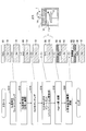
- FIG. 1 shows an example of a semiconductor structure of a MOS transistor.
- germanium Ge
- P-type n-type source and drain layers are formed.
- p-type source and drain layers are formed.
- a gate layer is formed between the source and drain layers.
- a High-k film high dielectric constant gate insulating film
- a passivation film is formed at the interface between the germanium substrate and the high-k film.
- the germanium (Ge) material has higher mobility than the silicon (Si) material.
- electron mobility (unit: cm 2 / V ⁇ s) is 1400 for silicon, and 3900 for germanium.
- III-V materials such as gallium arsenide (GaAs), indium gallium arsenide (InGaAs), indium arsenide (InAs), gallium antimonide (GaSb), and indium antimonide (InSb) are also more mobile than silicon materials. Is expensive.
- the mobility of electrons is 8500 for gallium arsenide, 12000 for indium gallium arsenide, 40000 for indium arsenide, 3000 for gallium antimonide, and 77000 for indium antimonide.
- the group III-V material is a compound of a group III (group 13) element and a group V (group 15) element of the periodic table, and is not limited to the above-described materials such as gallium arsenide.
- a silicon oxide film SiO 2
- a germanium substrate for example, alumina (Al 2 O 3 ) is used for the gate insulating film.
- the defect density at the interface 100 a between the silicon substrate 100 and the silicon oxide film 200 shown in FIG. 2A is on the order of 10 10 .
- the defect density at the interface 10a between the germanium substrate 10 shown in FIG. 2 (b) and germanium oxide film 20, 10 13 of the order of has three orders of magnitude higher than in the case of a silicon substrate .
- the surface of the germanium substrate 10 is treated with hydrogen sulfide (H 2 S) gas and ammonia (NH 3 ) gas, and germanium sulfide (GeS x ) passivation is performed on the surface of the germanium substrate 10.
- a film 30 is formed.
- the defect density on the surface of the germanium substrate 10 is on the order of 10 11 .
- the mobility of the manufactured semiconductor structure can be increased, and a high-performance transistor or other semiconductor structure can be manufactured.
- the germanium substrate 10 is transferred to the film forming apparatus 1 (step S12).
- the germanium substrate 10 is exposed to air for a predetermined time.
- the surface of the germanium substrate 10 is reoxidized, and a natural oxide film (GeO) 40 is formed on the germanium substrate 10. Due to the natural oxide film 40, the surface of the germanium substrate 10 has a high defect density.
- the germanium substrate 10 is etched in an NH 3 gas atmosphere using the same or different apparatus as the film forming apparatus 1 (step S14). By this step, the natural oxide film 40 on the surface of the germanium substrate 10 is substantially removed.
- the High-k film 50 includes alumina (Al 2 O 3 ), hafnium oxide (HfO 2 ), hafnium aluminate (HfAlO), zirconia oxide (ZrO 2 ), praseodymium oxide (PrO x ), and lanthanum oxide (LaO x ). Gadolinium oxide (Gd 2 O 3 ) may be used.
- a metal film 60 functioning as an upper electrode is formed (step S20), and this process is terminated.
- the metal film 60 tantalum (Ta), tantalum nitride (TaN), or titanium nitride (TiN) may be used.
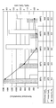
- FIG. 4 shows an example of the relationship between the time of exposure to air (ie, the time for which the germanium substrate is left) and the thickness of the native oxide on the germanium substrate.
- the horizontal axis in FIG. 4 indicates the standing time, and the vertical axis indicates the thickness of the natural oxide film.
- the thicknesses of the natural oxide films of the n-type germanium substrate (n-Ge) and the p-type germanium substrate (p-Ge) are the same as the natural thickness of the n-type silicon substrate (n-Si). It is 4 to 5 times the thickness of the oxide film. That is, the germanium substrate is more easily oxidized than the silicon substrate.
- the longer the standing time the more GeO x bonds are increased on the germanium substrate 10 and the GeS x bonds are decreased. Therefore, the longer the standing time, the lower the concentration of S on the germanium substrate 10 and the higher the O concentration. .
- the defect density at the interface between the germanium substrate 10 and the High-k film increases. That is, it can be seen that the germanium substrate 10 is more likely to be naturally oxidized than the silicon substrate, which increases the surface defect density and tends to decrease mobility.
- the germanium oxide (GeO 2 ) film 20 on the germanium substrate 10 can be almost removed by wet etching in step S10 of FIG. However, it is difficult to remove all the natural oxide film on the germanium substrate 10 by the wet etching. For this reason, it is preferable to make it difficult to form the natural oxide film 40 by shortening the time for which the germanium substrate 10 is left in step S ⁇ b> 12 (the transfer time or the like).
- the germanium substrate 10 is treated in step S16 of FIG. 3 to form and protect a passivation film on the surface of the germanium substrate 10, thereby preventing the surface of the germanium substrate 10 from being oxidized. To do. As a result, it is possible to prevent the defect density on the surface of the germanium substrate 10 from being increased and the device characteristics of the manufactured semiconductor structure from being deteriorated. For the above reason, it is more preferable that the processes after step S16 in FIG. 3 are performed in-situ in the film forming apparatus 1, for example. However, since a passivation film is formed on the surface of the germanium substrate 10 in step S16, steps S18 and S20 may be performed ex-situ.
- the film forming apparatus 1 has a cylindrical processing chamber C made of aluminum whose surface is anodized (anodized).
- a mounting table 12 is provided inside the processing chamber C.
- the mounting table 12 mounts the germanium substrate 10.
- a gas shower head 11 is provided on the ceiling of the processing chamber C. Hydrogen sulfide gas and ammonia gas are introduced from the gas introduction port 14 of the gas shower head 11 and supplied into the processing chamber C through the gas buffer space 11b and from a large number of gas vent holes 11a. A passivation film 30 is formed on the germanium substrate 10 by the action of hydrogen sulfide gas and ammonia gas supplied into the processing chamber C.
- step S16 in FIG. 3 the germanium substrate 10 is treated, and hydrogen sulfide (H 2 S) gas and ammonia (NH 3 ) gas are used to form a passivation film on the surface of the germanium substrate 10.
- H 2 S hydrogen sulfide
- NH 3 ammonia
- Treatment condition A is an ammonia / hydrogen sulfide gas ratio of 0/100.
- Treatment condition B is an ammonia / hydrogen sulfide gas ratio of 60/140.
- Treatment condition C is an ammonia / hydrogen sulfide gas ratio of 100/100.
- Treatment condition D is a ratio of ammonia / hydrogen sulfide gas of 140/60.
- Treatment condition E has an ammonia / hydrogen sulfide gas ratio of 0/100.
- Treatment condition F is an ammonia / hydrogen sulfide gas ratio of 100/100.
- the treatment conditions A and E differ from the other conditions B to D and F in that ammonia gas is not added.
- the treatment conditions A to D are different from the treatment conditions E and F in which the treatment time is 2 minutes and the treatment time is 20 minutes.
- the common points of treatment conditions A to F are as follows. Hydrochloric acid (HCL) wet etching (10% solution, 10 minutes) is performed before treatment. The pressure in the processing chamber is controlled to 100 Torr (13332 Pa), and the temperature is controlled to 100 ° C.
- HCL Hydrochloric acid
- FIG. 5B shows sulfur S observed as S2p orbital electrons by XPS (X-ray photoelectron spectroscopy) measurement of a passivation film (ie, the surface of a germanium substrate) formed under five treatment conditions. Indicates the percentage. For example, the treatment condition A indicates that 4% sulfur is present near the surface of the germanium substrate 10 on which the passivation film is formed.
- XPS X-ray photoelectron spectroscopy
- conditions B, C, D, and F in which ammonia gas is added to hydrogen sulfide gas for treatment are conditions A and A that are treated without adding ammonia gas to hydrogen sulfide gas.
- the ratio of sulfur S contained in the material of the passivation film is higher than that of E.
- the ratio of sulfur S contained in the passivation film is 6%.
- the ratio of sulfur S contained in the passivation film is about 10%.
- the sulfur S contained in the passivation film shown in FIG. 5B includes sulfur S that is not bonded to germanium Ge in the film. Therefore, next, the component of sulfur S bonded to Ge in the germanium substrate 10 will be considered.
- 6A to 6C show an example of the result of XPS measurement from the surface of the germanium substrate 10 on which the passivation film is formed. The horizontal axis represents the binding energy, and the vertical axis represents the composition state of the germanium substrate 10 surface.
- FIG. 6A shows a case where no treatment is performed (when a passivation film is not formed).
- FIG. 6B shows a case where treatment is performed without adding ammonia gas to hydrogen sulfide gas.
- FIG. 6C shows a case where treatment is performed by adding ammonia gas to hydrogen sulfide gas.
- the peak of GeS or GeS 2 contained in the passivation film is the case where the treatment without adding the ammonia gas in FIG. 6B is performed. which is significantly higher than the peak of GeS and GeS 2. That is, the passivation film when ammonia gas is added contains more sulfur S components bonded to Ge than when ammonia gas is not added.
- the passivation film when ammonia gas is added contains more sulfur S components bonded to Ge than when ammonia gas is not added.
- the GeS and GeS 2 peaks on the surface of the germanium substrate 10 are even lower than when the treatment is performed using hydrogen sulfide gas without adding the ammonia gas of FIG. 6B. It has become.
- the content of sulfur S is high, and it is found that GeS and GeS 2 bonded to germanium are stably present in the film. It was. Thereby, the defect density in the surface of a germanium substrate can be reduced and the mobility of the manufactured semiconductor can be improved.
- treatment time can be shortened by adding ammonia gas to hydrogen sulfide gas.
- the passivation film is usually formed using H 2 S gas at a high temperature of 300 ° C. to 400 ° C.
- ammonia gas is added to the hydrogen sulfide gas to lower the temperature of 100 ° C.
- a passivation film is formed at ° C.
- the upper and lower SEM (scanning electron microscope) images in FIG. 7A show the surface and cross section of the germanium substrate that has not been treated.
- the upper and lower SEM images in FIG. 7B show the surface and cross section of a germanium substrate treated with hydrogen sulfide gas and ammonia gas. 7A and 7B, it is proved that the surface roughness (roughness) of the germanium substrate treated with hydrogen sulfide gas and ammonia gas is equal to the surface roughness of the germanium substrate not treated. . In other words, it can be confirmed that even if treatment is performed with hydrogen sulfide gas and ammonia gas, the surface condition is not worse than the surface roughness of the germanium substrate before treatment.
- FIGS. 8A to 11 show the results of analyzing the surface state of a germanium substrate on which a passivation film is formed by TOF-SIMS (Time-of-Flight Secondary Mass Spectrometry).
- the temperature of the mounting table is shown as the temperature of the processing chamber.
- FIG. 8A shows the number of GeO 2 and the number of GeS in the passivation film when the pressure in the processing chamber is 3 Torr (400 Pa) and the temperature in the processing chamber is 25 ° C., 50 ° C., and 100 ° C. It is a graph.
- the horizontal axis indicates the temperature during the treatment, and the vertical axis indicates the ratio of GeO 2 to GeS. According to this result, the ratio of GeO 2 to GeS in the film is smaller at 50 ° C. and 100 ° C. than at 25 ° C.
- FIG. 8B shows the number of GeO 2 and the number of GeS in the passivation film when the pressure in the processing chamber is 50 Torr (6667 Pa) and the temperature in the processing chamber is 25 ° C., 50 ° C., and 100 ° C. It is a graph. As shown in FIG. 8C, the ratio of GeO 2 to GeS in the film is smaller at 50 ° C. and 100 ° C. than at 25 ° C.
- the ratio of GeO 2 to GeS decreases as the temperature increases in both cases where the pressure in the processing chamber is 3 Torr and 50 Torr, and as a result, the defect density decreases. From the above, when treatment is performed with hydrogen sulfide gas and ammonia gas, it is preferable to control the processing chamber to 50 ° C. or higher.
- the pressure in the processing chamber is preferably controlled to 3 Torr or more, and more preferably 50 Torr or more.
- FIG. 9 shows the number of GeO 2 and the number of GeS in the passivation film when the pressure in the processing chamber is controlled to 50 Torr and the temperature in the processing chamber is 25 ° C., 50 ° C., 100 ° C., 150 ° C., 200 ° C. 4 is a graph showing a ratio of GeO 2 to GeS.
- the temperature in the processing chamber is preferably 50 ° C. or higher because the O concentration on the surface of the germanium substrate can be reduced by controlling the temperature in the processing chamber to 50 ° C. or higher.
- the ratio of GeO 2 to GeS in the passivation film is in a saturated state and hardly changes.
- FIG. 10 shows the number of GeO x and the number of GeS x in the passivation film when the pressure in the processing chamber is controlled to 50 Torr and the temperature in the processing chamber is 25 ° C., 50 ° C., 100 ° C., 150 ° C., and 200 ° C. And a ratio of GeO x to GeS x .
- the number of GeO x is the total number of GeO and GeO 2
- the number of GeS x is the total number of GeS and GeS 2 .
- the temperature in the processing chamber is set to 50 ° C.
- the concentration of O on the surface of the germanium substrate can be reduced.
- the above is preferable. Further, in the range of 100 ° C. to 200 ° C., the ratio of GeO x to GeS x in the passivation film is in a saturated state and hardly changes.
- FIG. 11 is a graph showing the number of GeO 2 in the passivation film, the number of GeS, and the ratio of GeO 2 to GeS when the pressure and temperature in the processing chamber are controlled as described above.
- the pressure in the processing chamber is controlled to 100 Torr (13332 Pa) or higher, and the temperature is controlled to 100 ° C. or higher. Therefore, it is preferable to control as described above.
- the temperature of the mounting table may be controlled to 50 ° C. to 250 ° C.
- the pressure in the processing chamber may be controlled to 3 Torr or more.
- the upper limit of the pressure is preferably about 200 Torr (26664 Pa).
- the upper limit value of the practical range of APC is about 200 Torr, so that the pressure in the processing chamber is preferably controlled to 3 Torr to 200 Torr. Further, the upper limit is considered to be about 200 Torr in reducing the amount of processing gas used.
- FIG. 12 shows the result of analyzing the surface state of an indium gallium arsenide substrate on which a passivation film is formed by TOF-SIMS.
- an indium gallium arsenide substrate is wet-etched for 10 minutes with a liquid containing dilute hydrofluoric acid (DHF).
- DHF dilute hydrofluoric acid
- the treatment chamber temperature is controlled to 50 ° C.
- the pressure is controlled to 50 Torr (6666 Pa)
- treatment for 2 minutes is performed with hydrogen sulfide gas and ammonia gas.
- a passivation film is formed.
- FIG. 12 shows a case without treatment and a case with treatment.
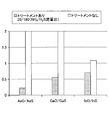
- FIG. 12 shows the ratio of AsO and AsS, the ratio of GaO and GaS, and the ratio of InO and InS in the passivation film thus formed.
- the ratio of AsO and AsS, the ratio of GaO and GaS, and the ratio of InO and InS are all higher in the concentration of S on the surface of the InGaAs substrate than in the case without treatment. It can be seen that the concentration is higher than the O concentration.
- a passivation film having a high sulfur S content is formed on the surface layer of a substrate such as germanium by a treatment in which ammonia gas is added to hydrogen sulfide gas. .
- the defect density on the surface of the substrate such as germanium that is, the interface between the substrate and the High-k film
- the treatment speed of treatment is increased by about 10 times faster by adding ammonia gas to hydrogen sulfide gas than in the case of performing treatment with only hydrogen sulfide gas without adding ammonia. it can.
- the passivation film can be formed at a low temperature of about 100 ° C. As a result, production efficiency can be improved.
- the passivation treatment method of this embodiment hydrogen sulfide gas and ammonia gas are used.
- hydrogen selenide (H 2 Se) gas may be used instead of hydrogen sulfide gas.
- a passivation film having a high selenium Se content is formed on a germanium or III-V substrate by a treatment in which ammonia gas is added to hydrogen selenide gas. The As a result, the defect density at the interface of the germanium or III-V substrate can be reduced.
- the passivation processing method according to the above embodiment is applied to the manufacture of a transistor.
- the passivation processing method according to the above embodiment can also be applied to capacitors including germanium and III-V groups.
- the defect density at the interface between germanium or a group III-V semiconductor and an oxide film formed thereon can be reduced.
- FIGS. 13A and 13B show the presence or absence of a treatment (passivation film) according to the present embodiment and the CV characteristics of the capacitor.
- FIG. 13A shows the characteristic (CV characteristic) of the capacitance C with respect to the voltage V of the capacitor when no treatment is performed on the germanium substrate according to the present embodiment.
- FIG. 13B shows the CV characteristics of the capacitor when the treatment according to this embodiment is performed.
- Each frequency is a frequency of power applied to the capacitor in the IC chip.
- the CV characteristics of the capacitor vary as shown by an ellipse U in FIG. 13A. That is, in this case, the defect density at the interface of the capacitor is high, and good characteristics are not obtained.
- a passivation film having a high sulfur S content is formed on a germanium or III-V substrate by a treatment in which ammonia gas is added to hydrogen sulfide gas. .
- the defect density at the interface of the germanium or III-V group substrate can be reduced and the mobility can be increased.
- a passivation film having a high selenium Se content is formed on a germanium or III-V substrate by a treatment in which ammonia gas is added to hydrogen selenide gas. .
- ammonia gas is added to hydrogen selenide gas.
- the passivation processing method, the semiconductor structure forming method, and the semiconductor structure have been described in the above embodiments.
- the passivation processing method, the semiconductor structure forming method, and the semiconductor structure according to the present invention are not limited to the above embodiments.
- Various modifications and improvements are possible within the scope of the present invention.
- the matters described in the plurality of embodiments can be combined within a consistent range.
- the passivation film may be formed by adding an inert gas such as N 2 in addition to hydrogen sulfide (H 2 S) gas or hydrogen selenide (H 2 Se) gas and ammonia (NH 3 ) gas.
- an inert gas such as N 2
- hydrogen sulfide (H 2 S) gas or hydrogen selenide (H 2 Se) gas and ammonia (NH 3 ) gas Good.
- the substrate to be processed according to the present invention is not limited to a wafer, and may be, for example, a large substrate for a flat panel display, an EL element, or a substrate for a solar cell.
- a thin film of a power generation layer such as CIGS (CuInGaSe2) or CZTS (Cu2ZnSnS4) is in an atmosphere of hydrogen sulfide gas to which ammonia is added or hydrogen selenide gas to which ammonia is added, and 100 ° C. to 500 ° C. It is formed at a temperature of ° C.
- the power generation layer formed at this time has a crystal structure in which the band gap is adjusted.
- Film forming apparatus 10 Germanium substrate 11: Gas shower head 12: Mounting table 20: Germanium oxide film 30: Passivation film 40: Natural oxide film 50: High-k film 60: Metal film C: Processing chamber
Landscapes
- Formation Of Insulating Films (AREA)
- Insulated Gate Type Field-Effect Transistor (AREA)
- Thin Film Transistor (AREA)
Abstract
【課題】ゲルマニウム又はIII-V族の材料の表面の欠陥密度を低くすることを目的とする。 【解決手段】ゲルマニウム(Ge)又はIII-V族の基板を処理室内の載置台に載置する工程と、硫化水素(H2S)ガス又はセレン化水素(H2Se)ガスと、アンモニア(NH3)ガスとを前記処理室内に供給し、前記基板の上に硫黄(S)又はセレン(Se)を含有するパッシベーション膜を成膜する工程と、を有するパッシベーション処理方法が提供される。
Description
本発明は、パッシベーション処理方法、半導体構造の形成方法及び半導体構造に関する。
ゲルマニウム(Ge)やインジウムガリウム砒素(InGaAs)等のIII-V族の材料は、シリコン(Si)材料と比較してモビリティ(移動度)が高い。そのため、次世代の集積回路の基板としてシリコンの替わりにゲルマニウム等を使用することが期待されている。しかしながら、ゲルマニウム等の基板と基板上に成膜する誘電体膜との界面の欠陥密度が高いことが、製造された半導体構造のモビリティを低下させる要因の一つとなっている。
そこで、欠陥密度を低くするために、ゲルマニウム等の基板の上に誘電体膜を成膜する前に、硫化水素(H2S)ガスで基板の上にパッシベーション膜を形成する方法が提案されている(例えば、特許文献1、2を参照)。
しかしながら、上記パッシベーション膜を形成する方法では、基板の温度を300℃~400℃の高温にする必要があり、かつ、パッシベーション膜の成膜時間が長いため、生産効率が悪くなるという課題がある。
これに対して、硫化アンモニウム(NH4)2Sを用いたウェットエッチングによりゲルマニウム基板の表面の欠陥密度を低くする方法が考えられる。しかし、この方法ではウェットエッチング後、ゲルマニウム基板が空気に暴露される。このため、ゲルマニウム基板の表面が再酸化され、ゲルマニウム基板の表面に欠陥密度の高い自然酸化膜が形成されてしまう。
上記課題に対して、一側面では、本発明は、ゲルマニウム又はIII-V族の材料の表面の欠陥密度を低くすることを目的とする。
上記課題を解決するために、一の態様によれば、ゲルマニウム(Ge)又はIII-V族の基板を処理室内の載置台に載置する工程と、硫化水素(H2S)ガス又はセレン化水素(H2Se)ガスと、アンモニア(NH3)ガスとを前記処理室内に供給し、前記基板の上に硫黄(S)又はセレン(Se)を含有するパッシベーション膜を成膜する工程と、を有するパッシベーション処理方法が提供される。
一の側面によれば、ゲルマニウム又はIII-V族の材料の表面の欠陥密度を低くすることができる。
以下、本発明を実施するための形態について図面を参照して説明する。なお、本明細書及び図面において、実質的に同一の構成については、同一の符号を付することにより重複した説明を省く。
[半導体構造例]
まず、本発明の一実施形態にかかる半導体構造の一例について、図1を参照しながら説明する。図1は、MOSトランジスタの半導体構造の一例を示す。本実施形態では、基板にゲルマニウム(Ge)を使用する。ゲルマニウム基板がP形の場合、n形のソース及びドレイン層が形成される。なお、ゲルマニウム基板がn形の場合、p形のソース及びドレイン層が形成される。ソース及びドレイン層間には、ゲート層が形成される。ゲート層及びゲルマニウム基板間には、High-k膜(高誘電率ゲート絶縁膜)が形成される。本実施形態では、ゲルマニウム基板とHigh-k膜との界面にパッシベーション膜が形成される。
まず、本発明の一実施形態にかかる半導体構造の一例について、図1を参照しながら説明する。図1は、MOSトランジスタの半導体構造の一例を示す。本実施形態では、基板にゲルマニウム(Ge)を使用する。ゲルマニウム基板がP形の場合、n形のソース及びドレイン層が形成される。なお、ゲルマニウム基板がn形の場合、p形のソース及びドレイン層が形成される。ソース及びドレイン層間には、ゲート層が形成される。ゲート層及びゲルマニウム基板間には、High-k膜(高誘電率ゲート絶縁膜)が形成される。本実施形態では、ゲルマニウム基板とHigh-k膜との界面にパッシベーション膜が形成される。
ゲルマニウム(Ge)材料は、シリコン(Si)材料と比較してモビリティ(移動度)が高い。例えば、電子のモビリティ(単位:cm2/V・s)は、シリコンが1400であるのに対して、ゲルマニウムは3900である。ガリウム砒素(GaAs)、インジウムガリウム砒素(InGaAs)、インジウム砒素(InAs)、アンチモン化ガリウム(GaSb)、アンチモン化インジウム(InSb)等のIII-V族の材料もまた、シリコン材料と比較してモビリティが高い。例えば、電子のモビリティは、ガリウム砒素が8500、インジウムガリウム砒素が12000、インジウム砒素が40000、アンチモン化ガリウムが3000、アンチモン化インジウムが77000である。なお、III-V族の材料は、周期表III族(13族)元素とV族(15族)元素との化合物であり、上記に示したガリウム砒素等の材料に限らない。
次世代の集積回路の基板としてシリコンの替わりにゲルマニウムやIII-V族の材料を使用し、高性能な半導体構造を製造することが期待される。しかしながら、ゲルマニウム基板とHigh-k膜等の誘電体膜(ゲート絶縁膜)との界面の欠陥密度が高いことが、製造された半導体構造のモビリティを低下させる要因の一つとなっている。
シリコン基板の場合、例えばゲート絶縁膜にはシリコン酸化膜(SiO2)が使われる。ゲルマニウム基板の場合、例えばゲート絶縁膜にはアルミナ(Al2O3)が使われる。
図2の(a)に示すシリコン基板100とシリコン酸化膜200との界面100aの欠陥密度は、1010のオーダである。これに対して、図2の(b)に示すゲルマニウム基板10と酸化ゲルマニウム膜20との界面10aの欠陥密度は、1013のオーダであり、シリコン基板の場合と比べて3桁高くなっている。
そこで、以下に説明する本実施形態では、ゲルマニウム基板10の表面を硫化水素(H2S)ガス及びアンモニア(NH3)ガスでトリートメントし、ゲルマニウム基板10の表面に硫化ゲルマニウム(GeSx)のパッシベーション膜30を形成する。これにより、図2の(c)に示すように、ゲルマニウム基板10の表面の欠陥密度は、1011のオーダになる。このようにして、本実施形態ではゲルマニウムの表面の欠陥密度を低くすることにより、製造された半導体構造のモビリティを高め、高性能なトランジスタやその他の半導体構造を製造することができる。
[半導体構造例:パッシベーション処理方法]
次に、本実施形態にかかるパッシベーション処理方法を用いた半導体構造の製造工程の一例について、図3のフローチャートを参照しながら説明する。本実施形態にかかる半導体構造では、まず、塩酸(HCL)又はDHF(Diluted Hydrofluoric acid:希フッ酸(HFとH2Oの混合液))の液体によりゲルマニウム基板10をウェットエッチングする(ステップS10)。この工程により、ゲルマニウム基板10上の酸化ゲルマニウム(GeO2)膜20が除去される。
次に、本実施形態にかかるパッシベーション処理方法を用いた半導体構造の製造工程の一例について、図3のフローチャートを参照しながら説明する。本実施形態にかかる半導体構造では、まず、塩酸(HCL)又はDHF(Diluted Hydrofluoric acid:希フッ酸(HFとH2Oの混合液))の液体によりゲルマニウム基板10をウェットエッチングする(ステップS10)。この工程により、ゲルマニウム基板10上の酸化ゲルマニウム(GeO2)膜20が除去される。
次に、ゲルマニウム基板10上にHigh-k膜を成膜するために、ゲルマニウム基板10を成膜装置1に搬送する(ステップS12)。この工程により、ゲルマニウム基板10は所定の時間だけ空気に暴露される。この放置時間にゲルマニウム基板10の表面が再酸化され、ゲルマニウム基板10に自然酸化膜(GeO)40が形成される。自然酸化膜40により、ゲルマニウム基板10の表面は欠陥密度が高い状態になる。
そこで、成膜装置1と同一又は異なる装置にてゲルマニウム基板10をNH3ガスの雰囲気にてエッチングする(ステップS14)。この工程により、ゲルマニウム基板10の表面の自然酸化膜40が概ね除去される。
次に、成膜装置1内に硫化水素(H2S)ガス及びアンモニア(NH3)ガスを供給し、ゲルマニウム基板10のトリートメントを行う(ステップS16)。この工程により、ゲルマニウム基板10の表面にGeSxのパッシベーション膜30が形成される。次に、High-k膜50を成膜する(ステップS18)。High-k膜50としては、アルミナ(Al2O3)、酸化ハフニウム(HfO2)、ハフニウムアルミネート(HfAlO)、酸化ジルコニア(ZrO2)、酸化プラセオジム(PrOx)、酸化ランタン(LaOx)、酸化ガドリニウム(Gd2O3)が使用されてもよい。
最後に、上部電極として機能する金属膜60を成膜し(ステップS20)、本処理を終了する。金属膜60としては、タンタル(Ta)、窒化タンタル(TaN),窒化チタン(TiN)が使用されてもよい。
(自然酸化膜)
なお、ステップS16以降の工程をin-situで行う環境が好ましい。ex-situで行う環境では、ステップS16のパッシベーション膜を成膜する前やステップS18のHigh-k膜50を成膜する前に、ゲルマニウム基板10の表面が空気に暴露されてしまい、その間にゲルマニウム基板10の表面に自然酸化膜40が形成されてしまう。例えば、図4は、空気に暴露する時間(すなわち、ゲルマニウム基板の放置時間)とゲルマニウム基板上の自然酸化物の厚さとの関係の一例を示す。図4の横軸は、放置時間を示し、縦軸は自然酸化膜の厚さを示す。なお、図4は、論文「Native Oxidation Growth on Ge(111) and (100) Surfaces」,Siti Kudnie Sahari, Hideki Murakami, Tomohiro Fujioka, Tatsuya Bando, Akio Ohta, Katsunori Makihara, Seiichiro Higashi, and Seiichi Miyazaki ,Japanese Journal of Applied Physics 50 (2011) 04DA12 のFig.6を引用する。
なお、ステップS16以降の工程をin-situで行う環境が好ましい。ex-situで行う環境では、ステップS16のパッシベーション膜を成膜する前やステップS18のHigh-k膜50を成膜する前に、ゲルマニウム基板10の表面が空気に暴露されてしまい、その間にゲルマニウム基板10の表面に自然酸化膜40が形成されてしまう。例えば、図4は、空気に暴露する時間(すなわち、ゲルマニウム基板の放置時間)とゲルマニウム基板上の自然酸化物の厚さとの関係の一例を示す。図4の横軸は、放置時間を示し、縦軸は自然酸化膜の厚さを示す。なお、図4は、論文「Native Oxidation Growth on Ge(111) and (100) Surfaces」,Siti Kudnie Sahari, Hideki Murakami, Tomohiro Fujioka, Tatsuya Bando, Akio Ohta, Katsunori Makihara, Seiichiro Higashi, and Seiichi Miyazaki ,Japanese Journal of Applied Physics 50 (2011) 04DA12 のFig.6を引用する。
これによれば、放置時間が同じ場合、n形ゲルマニウム基板(n-Ge)及びp形ゲルマニウム基板(p-Ge)の自然酸化膜の厚さは、n形シリコン基板(n-Si)の自然酸化膜の厚さに対して4~5倍になっている。つまり、ゲルマニウム基板は、シリコン基板よりも酸化しやすい。
よって、放置時間が長くなるほどゲルマニウム基板10上にGeOxの結合が増え、GeSxの結合が減るため、放置時間が長くなるほどゲルマニウム基板10上のSの濃度が低くなり、Oの濃度が高くなる。
ゲルマニウム基板10上のOの濃度が高くなると、ゲルマニウム基板10とHigh-k膜との界面における欠陥密度が高くなる。つまり、ゲルマニウム基板10は、シリコン基板よりも自然酸化され易く、これによって表面の欠陥密度が高くなり、モビリティが下がる傾向があることがわかる。
ゲルマニウム基板10上の酸化ゲルマニウム(GeO2)膜20は、図3のステップS10のウェットエッチングでほぼ除去できる。しかし、ゲルマニウム基板10上の自然酸化膜は上記のウェットエッチングですべて除去することは難しい。このため、ステップS12のゲルマニウム基板10の放置時間(搬送時間等)を短縮することで、自然酸化膜40が形成され難いようにすることが好ましい。
したがって、前記放置時間の管理は重要である。本実施形態では、図3のステップS16において、ゲルマニウム基板10のトリートメントを行い、ゲルマニウム基板10の表面にパッシベーション膜を形成し、保護し、これにより、ゲルマニウム基板10の表面が酸化されることを防止する。この結果、ゲルマニウム基板10の表面の欠陥密度が高くなり、製造された半導体構造のデバイス特性が悪くなることを防ぐことができる。なお、以上の理由から図3のステップS16以降の工程は、例えば成膜装置1においてin-situで行うことがより好ましい。ただし、ステップS16にてゲルマニウム基板10の表面にパッシベーション膜が形成されているため、ステップS18及びステップS20はex-situで行ってもよい。
(成膜装置の構成例)
なお、成膜装置の構成例について簡単に説明する。成膜装置1は、表面がアルマイト処理(陽極酸化処理)されたアルミニウムからなる円筒形の処理室Cを有している。処理室Cの内部には載置台12が設けられている。載置台12は、ゲルマニウム基板10を載置する。
なお、成膜装置の構成例について簡単に説明する。成膜装置1は、表面がアルマイト処理(陽極酸化処理)されたアルミニウムからなる円筒形の処理室Cを有している。処理室Cの内部には載置台12が設けられている。載置台12は、ゲルマニウム基板10を載置する。
処理室Cの天井部には、ガスシャワーヘッド11が設けられている。硫化水素ガス及びアンモニアガスは、ガスシャワーヘッド11のガス導入口14から導入され、ガスバッファ空間11bを通って多数のガス通気孔11aから処理室C内に供給される。処理室C内へ供給された硫化水素ガス及びアンモニアガスの作用によりゲルマニウム基板10上にパッシベーション膜30が成膜される。
(NH3添加)
図3のステップS16では、ゲルマニウム基板10のトリートメントを行い、ゲルマニウム基板10の表面にパッシベーション膜を形成するために硫化水素(H2S)ガス及びアンモニア(NH3)ガスを用いた。次に、5つのトリートメント条件に対して成膜されたパッシベーション膜について、図5Aおよび図5Bを参照しながら説明する。図5Aは、5つのトリートメント条件を示す。
図3のステップS16では、ゲルマニウム基板10のトリートメントを行い、ゲルマニウム基板10の表面にパッシベーション膜を形成するために硫化水素(H2S)ガス及びアンモニア(NH3)ガスを用いた。次に、5つのトリートメント条件に対して成膜されたパッシベーション膜について、図5Aおよび図5Bを参照しながら説明する。図5Aは、5つのトリートメント条件を示す。
トリートメント条件Aは、アンモニア/硫化水素ガスの比が、0/100である。
トリートメント条件Bは、アンモニア/硫化水素ガスの比が、60/140である。
トリートメント条件Cは、アンモニア/硫化水素ガスの比が、100/100である。
トリートメント条件Dは、アンモニア/硫化水素ガスの比が、140/60である。
トリートメント条件Eは、アンモニア/硫化水素ガスの比が、0/100である。
トリートメント条件Fは、アンモニア/硫化水素ガスの比が、100/100である。
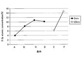
つまり、トリートメント条件A、Eは、アンモニアガスが添加されていない点が他の条件B~D,Fと異なる。また、トリートメント条件A~Dは、トリートメント時間が2分であり、トリートメント時間が20分のトリートメント条件E、Fと異なる。
トリートメント条件A~Fの共通点は以下である。
・塩酸(HCL)のウェットエッチング(10%の溶液、10分)がトリートメント前に実行されている。
・処理室内の圧力は100Torr(13332Pa)、温度は100℃に制御されている。
・塩酸(HCL)のウェットエッチング(10%の溶液、10分)がトリートメント前に実行されている。
・処理室内の圧力は100Torr(13332Pa)、温度は100℃に制御されている。
図5Bは、5つのトリートメント条件下で成膜されたパッシベーション膜(つまり、ゲルマニウム基板の表面)のXPS(X線光電子分光:X-ray Photoelectron Spectroscopy)測定によるS2p軌道電子として観測された硫黄Sの割合を示す。例えば、トリートメント条件Aでは、パッシベーション膜が形成されたゲルマニウム基板10の表面付近に4%の硫黄が存在していることを示す。
図5Aおよび図5Bによれば、硫化水素ガスにアンモニアガスを添加してトリートメントを行った条件B、C、D、Fは、硫化水素ガスにアンモニアガスを添加せずにトリートメントを行った条件A、Eよりもパッシベーション膜の物質に含まれる硫黄Sの割合が多いことがわかる。特に、硫化水素ガスにアンモニアガスを添加せずに20分間トリートメントを行った条件Eの場合、パッシベーション膜に含まれる硫黄Sの割合は6%である。これに対して、硫化水素ガスにアンモニアガスを添加して2分間トリートメントを行った条件B~Dの場合、パッシベーション膜に含まれる硫黄Sの割合は10%程度である。つまり、硫化水素ガスにアンモニアガスを添加してトリートメントを行うと、トリートメント時間を1/10に短縮してもパッシベーション膜に含まれるSの割合は高くなり、ゲルマニウム基板10の表面の欠陥密度を低くすることができることがわかる。
ただし、図5Bに示されるパッシベーション膜に含まれる硫黄Sには、膜中のゲルマニウムGeと結合していない硫黄Sも含まれる。よって、次に、ゲルマニウム基板10中のGeと結合している硫黄Sの成分について考察する。図6A乃至図6Cは、パッシベーション膜が形成されたゲルマニウム基板10を表面からXPS測定した結果の一例を示す。横軸は結合エネルギーであり、縦軸はゲルマニウム基板10表面の組成の状態を示す。図6Aは、トリートメントを行っていない場合(パッシベーション膜が形成されていない場合)を示す。図6Bは、硫化水素ガスにアンモニアガスを添加せずにトリートメントを行った場合を示す。図6Cは、硫化水素ガスにアンモニアガスを添加してトリートメントを行った場合を示す。
図6A乃至図6Cの測定結果によれば、図6Cのアンモニアガスを添加したトリートメントでは、パッシベーション膜に含まれるGeSやGeS2のピークが、図6Bのアンモニアガスを添加しないトリートメントを行った場合のGeSやGeS2のピークよりも顕著に高くなっている。つまり、アンモニアガスを添加した場合のパッシベーション膜には、アンモニアガスを添加しない場合よりもGeと結合した硫黄Sの成分が多く含まれる。このように、アンモニアガスを添加した硫化水素ガスを用いてトリートメントを行うことで、GeSxを形成する際の活性化エネルギーが下がると推測される。
以上から、アンモニアガスを添加した硫化水素ガスを用いてトリートメントを行うことで、ゲルマニウムと結合しているSがパッシベーション膜中に含まれる割合が高くなり、ゲルマニウム基板10表面の欠陥密度が低下することがわかる。これにより、ゲルマニウム基板10とHigh-k膜50との界面の状態がよくなって、モビリティが高くなると予想される。
なお、図6Aのトリートメントを行っていない場合、ゲルマニウム基板10表面のGeSやGeS2のピークは、図6Bのアンモニアガスを添加せずに硫化水素ガスを用いてトリートメントを行った場合よりも更に低くなっている。
以上に説明したように、本実施形態によるパッシベーション処理方法により形成したパッシベーション膜では、硫黄Sの含有率が高くなり、ゲルマニウムと結合したGeSやGeS2として安定して膜中に存在することがわかった。これにより、ゲルマニウム基板の表面における欠陥密度を低下させ、製造された半導体のモビリティを向上させることができる。
また、硫化水素ガスにアンモニアガスを添加することでトリートメント時間を短縮することができる。また、通常300℃~400℃の高温にてH2Sガスを用いてパッシベーション膜が成膜されるのに対し、本実施形態では、硫化水素ガスにアンモニアガスを添加して、より低温の100℃でパッシベーション膜を形成する。この結果、トリートメント時間を約1/10に短縮でき、かつ低温処理にてパッシベーション膜を形成することができ、生産効率を向上させることができる。
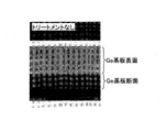
なお、図7Aの上段及び下段のSEM(走査型電子顕微鏡)画像には、トリートメントを行っていないゲルマニウム基板の表面及び断面を示す。図7Bの上段及び下段のSEM画像には、硫化水素ガスとアンモニアガスによりトリートメントを行ったゲルマニウム基板の表面及び断面を示す。図7Aおよび図7Bによれば、硫化水素ガスとアンモニアガスによりトリートメントを行ったゲルマニウム基板の表面粗さ(roughness)が、トリートメントを行っていないゲルマニウム基板の表面粗さと同等であることが証明される。つまり、硫化水素ガスとアンモニアガスによりトリートメントを行っても、トリートメント前のゲルマニウム基板の表面粗さよりも表面状態が悪くならないことが確認できる。
[温度及び圧力依存]
次に、本実施形態にかかるパッシベーション処理方法を適用する処理室の温度及び圧力依存性について、図8A~図11を参照しながら説明する。図8A~図11は、TOF-SIMS(Time-of-Flight Secondary Mass Spectrometry:二次イオン質量分析法)によりパッシベーション膜が形成されたゲルマニウム基板の表面状態を分析した結果を示す。
次に、本実施形態にかかるパッシベーション処理方法を適用する処理室の温度及び圧力依存性について、図8A~図11を参照しながら説明する。図8A~図11は、TOF-SIMS(Time-of-Flight Secondary Mass Spectrometry:二次イオン質量分析法)によりパッシベーション膜が形成されたゲルマニウム基板の表面状態を分析した結果を示す。
本実施形態では、処理室の温度として載置台の温度が示されている。
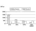
ここでは、まず、塩酸(HCL)を含む液体でゲルマニウム基板10を10分間ウェットエッチングする。次に、ウェットエッチング後のゲルマニウム基板に、硫化水素ガス及びアンモニアガスによりトリートメントを行った結果の一例を示す。図8Aは、処理室内の圧力が3Torr(400Pa)の場合であって、処理室内の温度が25℃、50℃、100℃のときのパッシベーション膜中のGeO2の個数とGeSの個数とを示したグラフである。図8Cは、横軸がトリートメント時の温度を示し、縦軸がGeSに対するGeO2の比率を示す。この結果によれば、膜中のGeSに対するGeO2の比率は、25℃よりも50℃及び100℃の方が少なくなっている。
図8Bは、処理室内の圧力が50Torr(6667Pa)の場合であって、処理室内の温度が25℃、50℃、100℃のときのパッシベーション膜中のGeO2の個数とGeSの個数とを示したグラフである。図8Cに示すように、膜中のGeSに対するGeO2の比率は、25℃よりも50℃及び100℃の方が少なくなっている。
このように、処理室内の圧力が3Torr及び50Torrのいずれの場合も温度が高くなるほどGeSに対するGeO2の比率は低くなり、この結果、欠陥密度が低下する。以上から、硫化水素ガスとアンモニアガスによりトリートメントを行う際、処理室内を50℃以上に制御することが好ましい。
また、硫化水素ガスとアンモニアガスによりトリートメントを行う際、処理室内の圧力は3Torr以上に制御することが好ましく、50Torr以上の高圧にするとより好ましい。
図9は、処理室内の圧力を50Torrに制御し、処理室内の温度を25℃、50℃、100℃、150℃、200℃にしたときのパッシベーション膜中のGeO2の個数、GeSの個数、およびGeSに対するGeO2の比率を示したグラフである。これによれば、硫化水素ガスとアンモニアガスによりトリートメントを行う際、処理室内の温度を50℃以上に制御するとゲルマニウム基板の表面のOの濃度を低下できるため処理室内の温度は50℃以上が好ましい。また、処理室内の温度が100℃~200℃の範囲では、パッシベーション膜中のGeSに対するGeO2の割合が飽和状態にあり、ほぼ変化していない。
図10は、処理室内の圧力を50Torrに制御し、処理室内の温度を25℃、50℃、100℃、150℃、200℃にしたときのパッシベーション膜中のGeOxの個数、GeSxの個数、およびGeSxに対するGeOxの比率を示したグラフである。本例では、GeOxの個数は、GeOとGeO2の個数の合計であり、GeSxの個数は、GeSとGeS2の個数の合計である。図10に示されるように、硫化水素ガスとアンモニアガスによりトリートメントを行う際、処理室内の温度を50℃以上にするとゲルマニウム基板の表面のOの濃度を低下できるため、処理室内の温度は50℃以上が好ましい。また、100℃~200℃の範囲ではパッシベーション膜中のGeSxに対するGeOxの割合が飽和状態にあり、ほぼ変化していない。
図11の実験では、処理室内の圧力を50Torr(6667Pa)、100Torr(13332Pa)、300Torr(39996Pa)、500Torr(66670Pa)に制御し、処理室内の温度を100℃、200℃、250℃に制御する。図11は、処理室内の圧力および温度を上述のように制御したときのパッシベーション膜中のGeO2の個数とGeSの個数とGeSに対するGeO2の比率とを示したグラフである。図11に示されるように、硫化水素ガスとアンモニアガスによりトリートメントを行う際、処理室内の圧力を100Torr(13332Pa)以上に制御し、温度を100℃以上に制御すると、概ねゲルマニウム基板の表面のOの濃度を低下できるため、上述のように制御することが好ましい。
また、Tにて差し示す枠内の結果によれば、同じ圧力で温度を上げるとパッシベーション膜に含まれるOの数が増えている。また、Pにて差し示す枠内の結果によれば、同じ温度で圧力を上げるとパッシベーション膜に含まれるOの数が減っている。ただし、GeSに対するGeO2の比率を考慮すると、載置台の温度は50℃~250℃に制御すればよい。また、処理室の圧力は3Torr以上に制御すればよい。また、圧力の上限値は、200Torr(26664Pa)程度が好ましい。APC(自動圧力制御器)を動作させて処理室内を調圧する場合、APCの実用範囲の上限値が200Torr程度であるため、処理室の圧力は、3Torr~200Torrに制御することが好ましい。また、処理ガスの使用量を少なくする上でも、上限値は200Torr程度になると思われる。
[インジウムガリウム砒素基板と流量依存]
次に、本実施形態にかかるパッシベーション処理方法におけるガスの流量依存性について、図12を参照しながら説明する。ここでは、ゲルマニウム基板の替わりにインジウムガリウム砒素(InGaAs)の基板が使用される。インジウムガリウム砒素の基板は、本実施形態にかかるパッシベーション処理方法を適用するIII-V族の基板の一例である。III-V族の他の材料としては、ガリウム砒素(GaAs)、インジウム砒素(InAs)、アンチモン化ガリウム(GaSb)及びアンチモン化インジウム(InSb)等を使用することができる。なお、図12は、TOF-SIMSによりパッシベーション膜が形成されたインジウムガリウム砒素の基板の表面状態を分析した結果を示す。
次に、本実施形態にかかるパッシベーション処理方法におけるガスの流量依存性について、図12を参照しながら説明する。ここでは、ゲルマニウム基板の替わりにインジウムガリウム砒素(InGaAs)の基板が使用される。インジウムガリウム砒素の基板は、本実施形態にかかるパッシベーション処理方法を適用するIII-V族の基板の一例である。III-V族の他の材料としては、ガリウム砒素(GaAs)、インジウム砒素(InAs)、アンチモン化ガリウム(GaSb)及びアンチモン化インジウム(InSb)等を使用することができる。なお、図12は、TOF-SIMSによりパッシベーション膜が形成されたインジウムガリウム砒素の基板の表面状態を分析した結果を示す。
ここでは、まず、希フッ酸(DHF)を含む液体でインジウムガリウム砒素の基板を10分間ウェットエッチングする。次に、処理室の温度を50℃、圧力を50Torr(6666Pa)に制御し、硫化水素ガスとアンモニアガスとにより2分間のトリートメントが行われる。この工程により、パッシベーション膜が成膜される。
ゲルマニウム基板の場合、ゲルマニウム基板の表面のGeOx及びGeSxの個数を測定することでそれらの比率からパッシベーション膜の特性を考察した。これに対して、インジウムガリウム砒素(InGaAs)の基板の場合、InGaAsの基板の表面のInOx、InSx、GaOx、GaSx、AsOx及びAsSxの個数を測定する。そして、インジウム(In)、ガリウム(Ga)、砒素(As)のそれぞれについて、Sに対するOの比率を考察する。図12には、トリートメントなしの場合と、トリートメントありの場合が示されている。ここで「トリートメントあり」とは、アンモニアガスと硫化水素ガスの流量比が20/180の場合にアンモニアガスと硫化水素ガスのトリートメントである。図12には、これにより形成されたパッシベーション膜中のAsO及びAsSの比率、GaO及びGaSの比率、InO及びInSの比率が示されている。図12によれば、AsO及びAsSの比率、GaO及びGaSの比率、InO及びInSの比率のいずれも、トリートメントありの場合には、トリートメントなしの場合よりもInGaAsの基板の表面のSの濃度がOの濃度よりも高くなっていることがわかる。この結果、硫化水素ガスに対するアンモニアガスの流量比を10%(=20/(20+180)×100)以上に制御することが好ましい。なお、図12の結果ではAsO/AsS < GaO/GaS < InO/InSとなっている。
以上に説明したように、本実施形態のパッシベーション処理方法によれば、硫化水素ガスにアンモニアガスを添加したトリートメントにより硫黄Sの含有率が高いパッシベーション膜がゲルマニウム等の基板の表層に成膜される。これにより、ゲルマニウム等の基板の表面(つまり、基板とHigh-k膜との界面)における欠陥密度を低下させることができる。
また、本実施形態によれば、硫化水素ガスにアンモニアガスを添加することでトリートメントの処理スピードを、アンモニアを添加せずに硫化水素ガスのみによりトリートメントを行う場合と比較して10倍程高速にできる。また、通常、トリートメントが300℃程度の高温で行われるのに対し、本実施形態によれば、100℃程度の低温にてパッシベーション膜を形成することができる。この結果、生産効率を向上させることができる。
なお、本実施形態のパッシベーション処理方法では、硫化水素ガスとアンモニアガスとを使用した。しかしながら、硫化水素ガスの替わりにセレン化水素(H2Se)ガスを使用してもよい。この場合、本実施形態のパッシベーション処理方法によれば、セレン化水素ガスにアンモニアガスを添加したトリートメントによりセレンSeの含有率が高いパッシベーション膜がゲルマニウムやIII-V族の基板の上に成膜される。これにより、ゲルマニウムやIII-V族の基板の界面における欠陥密度を低下させることができる。
[キャパシタへの応用]
上記実施形態にかかるパッシベーション処理方法は、トランジスタの製造に適用される。しかしながら、上記実施形態にかかるパッシベーション処理方法は、ゲルマニウムやIII-V族を含むキャパシタにも適用可能である。上記実施形態にかかるパッシベーション処理方法により、ゲルマニウムやIII-V族半導体とその上に形成される酸化膜との界面の欠陥密度を低下させることができる。
上記実施形態にかかるパッシベーション処理方法は、トランジスタの製造に適用される。しかしながら、上記実施形態にかかるパッシベーション処理方法は、ゲルマニウムやIII-V族を含むキャパシタにも適用可能である。上記実施形態にかかるパッシベーション処理方法により、ゲルマニウムやIII-V族半導体とその上に形成される酸化膜との界面の欠陥密度を低下させることができる。
図13Aおよび図13Bは、本実施形態にかかるトリートメント(パッシベーション膜)の有無とキャパシタのC-V特性を示す。図13Aは、本実施形態にかかるゲルマニウム基板に対してトリートメントを行わなかった場合のキャパシタの電圧Vに対する容量Cの特性(C-V特性)を示す。図13Bは、本実施形態にかかるトリートメントを行なった場合のキャパシタのC-V特性を示す。各周波数は、ICチップ内のキャパシタに印加する電力の周波数である。
図13Aおよび図13Bによれば、硫化水素ガスにアンモニアガスを添加してパッシベーション膜を成膜した場合、パッシベーション膜によりキャパシタのC-V特性が良好になっている。特に、図13Bの楕円Wに示すように、曲線F1(1MHz)、曲線F2(500kHz)、曲線F3(200kHz)、曲線F4(100kHz)において良好なC-V特性が得られている。つまり、キャパシタの界面の欠陥密度が低い場合、周波数が高くても(例えば、100kHz、200kHz、500kHz)、良好な特性が得られている。
これに対して、本実施形態にかかるトリートメントを行なっていない場合、図13Aの楕円Uに示すように、キャパシタのC-V特性にバラツキがある。つまり、この場合、キャパシタの界面の欠陥密度が高く、良好な特性が得られていない。
以上から、本実施形態のパッシベーション処理方法によれば、硫化水素ガスにアンモニアガスを添加したトリートメントにより硫黄Sの含有率が高いパッシベーション膜がゲルマニウムやIII-V族の基板の上に成膜される。これにより、ゲルマニウムやIII-V族の基板の界面における欠陥密度を低下させ、モビリティを高めることができる。
また、本実施形態のパッシベーション処理方法によれば、セレン化水素ガスにアンモニアガスを添加したトリートメントによりセレンSeの含有率が高いパッシベーション膜がゲルマニウムやIII-V族の基板の上に成膜される。これにより、ゲルマニウムやIII-V族の基板の界面における欠陥密度を低下させ、モビリティを高めることができる。
以上、パッシベーション処理方法、半導体構造の形成方法及び半導体構造を上記実施形態により説明したが、本発明にかかるパッシベーション処理方法、半導体構造の形成方法及び半導体構造は上記実施形態に限定されるものではなく、本発明の範囲内で種々の変形及び改良が可能である。また、上記複数の実施形態に記載された事項は、矛盾しない範囲で組み合わせることができる。
例えば、パッシベーション膜を成膜する工程は、硫化水素(H2S)ガス又はセレン化水素(H2Se)ガスと、アンモニア(NH3)ガスに加えてN2等の不活性ガスを加えてもよい。ただし、硫化水素ガス又はセレン化水素ガスの分圧は他のガスの分圧よりも高く制御することが好ましい。
また、本発明により処理される基板は、ウェハに限られず、例えば、フラットパネルディスプレイ(Flat Panel Display)用の大型基板、EL素子又は太陽電池用の基板であってもよい。太陽電池用の基板の場合、CIGS(CuInGaSe2)、CZTS(Cu2ZnSnS4)等の発電層の薄膜が、アンモニアを添加した硫化水素ガス又はアンモニアを添加したセレン化水素ガスの雰囲気で、かつ100℃~500℃の温度で形成される。このとき形成される発電層は、バンドギャップが調整された結晶構造を有する。
本国際特許出願は2015年4月20日に出願した日本国特許出願第2015-086251号に基づきその優先権を主張するものであり、日本国特許出願第2015-086251号の全内容を本願に援用する。
1:成膜装置
10:ゲルマニウム基板
11:ガスシャワーヘッド
12:載置台
20:酸化ゲルマニウム膜
30:パッシベーション膜
40:自然酸化膜
50:High-k膜
60:金属膜
C:処理室
10:ゲルマニウム基板
11:ガスシャワーヘッド
12:載置台
20:酸化ゲルマニウム膜
30:パッシベーション膜
40:自然酸化膜
50:High-k膜
60:金属膜
C:処理室
Claims (7)
- ゲルマニウム(Ge)又はIII-V族の基板を処理室内の載置台に載置する工程と、
硫化水素(H2S)ガス又はセレン化水素(H2Se)ガスと、アンモニア(NH3)ガスとを前記処理室内に供給し、前記基板の上に硫黄(S)又はセレン(Se)を含有するパッシベーション膜を成膜する工程と、
を有するパッシベーション処理方法。 - 前記載置台の温度を50℃~250℃に制御する、
請求項1に記載のパッシベーション処理方法。 - 前記処理室の圧力を3Torr~200Torrに制御する、
請求項1に記載のパッシベーション処理方法。 - 硫化水素(H2S)ガスに対するアンモニア(NH3)ガスの流量比を10%以上に制御する、
請求項1に記載のパッシベーション処理方法。 - 硫化水素(H2S)ガス又はセレン化水素(H2Se)ガスと、アンモニア(NH3)ガスとともに不活性ガスを供給する、
請求項1に記載のパッシベーション処理方法。 - 半導体構造の形成方法であって、
ゲルマニウム(Ge)又はIII-V族の基板を処理室内の載置台に載置する工程と、
硫化水素(H2S)ガス又はセレン化水素(H2Se)ガスと、アンモニア(NH3)ガスとを前記処理室内に供給し、前記基板の上に硫黄(S)又はセレン(Se)を含有するパッシベーション膜を成膜する工程と、
前記パッシベーション膜の上に誘電体膜を形成する工程と、
前記誘電体膜の上に金属膜を形成する工程と、
を有する、半導体構造の形成方法。 - ゲルマニウム(Ge)又はIII-V族の基板と、
硫化水素(H2S)ガス又はセレン化水素(H2Se)ガスと、アンモニア(NH3)ガスとにより、前記基板の上に形成された硫黄(S)又はセレン(Se)を含有するパッシベーション膜と、
前記パッシベーション膜の上に形成された誘電体膜と、
前記誘電体膜の上に形成された金属膜と、
を有する半導体構造。
Priority Applications (1)
| Application Number | Priority Date | Filing Date | Title |
|---|---|---|---|
| KR1020177030094A KR20170127567A (ko) | 2015-04-20 | 2016-04-06 | 패시베이션 처리 방법, 반도체 구조의 형성 방법 및 반도체 구조 |
Applications Claiming Priority (2)
| Application Number | Priority Date | Filing Date | Title |
|---|---|---|---|
| JP2015086251A JP2016207789A (ja) | 2015-04-20 | 2015-04-20 | パッシベーション処理方法、半導体構造の形成方法及び半導体構造 |
| JP2015-086251 | 2015-04-20 |
Publications (1)
| Publication Number | Publication Date |
|---|---|
| WO2016170988A1 true WO2016170988A1 (ja) | 2016-10-27 |
Family
ID=57143890
Family Applications (1)
| Application Number | Title | Priority Date | Filing Date |
|---|---|---|---|
| PCT/JP2016/061322 Ceased WO2016170988A1 (ja) | 2015-04-20 | 2016-04-06 | パッシベーション処理方法、半導体構造の形成方法及び半導体構造 |
Country Status (4)
| Country | Link |
|---|---|
| JP (1) | JP2016207789A (ja) |
| KR (1) | KR20170127567A (ja) |
| TW (1) | TW201642344A (ja) |
| WO (1) | WO2016170988A1 (ja) |
Cited By (7)
| Publication number | Priority date | Publication date | Assignee | Title |
|---|---|---|---|---|
| JP2018022715A (ja) * | 2016-08-01 | 2018-02-08 | 株式会社Screenホールディングス | ドーパント導入方法 |
| CN113228235A (zh) * | 2018-12-18 | 2021-08-06 | 昭和电工株式会社 | 附着物除去方法和成膜方法 |
| CN113261082A (zh) * | 2018-12-25 | 2021-08-13 | 昭和电工株式会社 | 附着物除去方法和成膜方法 |
| CN113261081A (zh) * | 2018-12-25 | 2021-08-13 | 昭和电工株式会社 | 附着物除去方法和成膜方法 |
| CN113840941A (zh) * | 2019-12-17 | 2021-12-24 | 昭和电工株式会社 | 钝化膜的制造方法 |
| CN113874547A (zh) * | 2019-11-12 | 2021-12-31 | 昭和电工株式会社 | 附着物除去方法及成膜方法 |
| CN113906155A (zh) * | 2019-11-19 | 2022-01-07 | 昭和电工株式会社 | 附着物除去方法和成膜方法 |
Citations (6)
| Publication number | Priority date | Publication date | Assignee | Title |
|---|---|---|---|---|
| JPS58141576A (ja) * | 1982-02-17 | 1983-08-22 | Nec Corp | 電界効果型トランジスタ |
| JPH04236424A (ja) * | 1991-01-18 | 1992-08-25 | Hitachi Cable Ltd | 絶縁膜付き半導体ウェハ及びその製造方法 |
| JP2007123895A (ja) * | 2005-10-26 | 2007-05-17 | Internatl Business Mach Corp <Ibm> | 方法および半導体構造(非酸素カルコゲン不活性化ステップを用いて製作されたGe系半導体構造) |
| US20100163937A1 (en) * | 2008-12-31 | 2010-07-01 | Scott Bruce Clendenning | Methods of forming nickel sulfide film on a semiconductor device |
| JP2011091394A (ja) * | 2009-10-02 | 2011-05-06 | Imec | 誘電体とiii/v化合物との間の低欠陥界面の製造方法 |
| WO2016007733A1 (en) * | 2014-07-10 | 2016-01-14 | Tokyo Electron Limited | Gas phase oxide removal and passivation of germainium-containing semiconductors and compound semiconductors |
-
2015
- 2015-04-20 JP JP2015086251A patent/JP2016207789A/ja active Pending
-
2016
- 2016-04-06 KR KR1020177030094A patent/KR20170127567A/ko not_active Ceased
- 2016-04-06 WO PCT/JP2016/061322 patent/WO2016170988A1/ja not_active Ceased
- 2016-04-18 TW TW105111968A patent/TW201642344A/zh unknown
Patent Citations (6)
| Publication number | Priority date | Publication date | Assignee | Title |
|---|---|---|---|---|
| JPS58141576A (ja) * | 1982-02-17 | 1983-08-22 | Nec Corp | 電界効果型トランジスタ |
| JPH04236424A (ja) * | 1991-01-18 | 1992-08-25 | Hitachi Cable Ltd | 絶縁膜付き半導体ウェハ及びその製造方法 |
| JP2007123895A (ja) * | 2005-10-26 | 2007-05-17 | Internatl Business Mach Corp <Ibm> | 方法および半導体構造(非酸素カルコゲン不活性化ステップを用いて製作されたGe系半導体構造) |
| US20100163937A1 (en) * | 2008-12-31 | 2010-07-01 | Scott Bruce Clendenning | Methods of forming nickel sulfide film on a semiconductor device |
| JP2011091394A (ja) * | 2009-10-02 | 2011-05-06 | Imec | 誘電体とiii/v化合物との間の低欠陥界面の製造方法 |
| WO2016007733A1 (en) * | 2014-07-10 | 2016-01-14 | Tokyo Electron Limited | Gas phase oxide removal and passivation of germainium-containing semiconductors and compound semiconductors |
Cited By (13)
| Publication number | Priority date | Publication date | Assignee | Title |
|---|---|---|---|---|
| JP2018022715A (ja) * | 2016-08-01 | 2018-02-08 | 株式会社Screenホールディングス | ドーパント導入方法 |
| CN113228235A (zh) * | 2018-12-18 | 2021-08-06 | 昭和电工株式会社 | 附着物除去方法和成膜方法 |
| CN113228235B (zh) * | 2018-12-18 | 2024-03-19 | 株式会社力森诺科 | 附着物除去方法和成膜方法 |
| CN113261081A (zh) * | 2018-12-25 | 2021-08-13 | 昭和电工株式会社 | 附着物除去方法和成膜方法 |
| EP3905309A4 (en) * | 2018-12-25 | 2022-03-16 | Showa Denko K.K. | DEPOSIT REMOVAL METHODS AND FILM FORMING METHODS |
| CN113261082A (zh) * | 2018-12-25 | 2021-08-13 | 昭和电工株式会社 | 附着物除去方法和成膜方法 |
| CN113261081B (zh) * | 2018-12-25 | 2024-04-12 | 株式会社力森诺科 | 附着物除去方法和成膜方法 |
| US12116675B2 (en) | 2018-12-25 | 2024-10-15 | Resonac Corporation | Adhesion removal method and film-forming method |
| CN113874547A (zh) * | 2019-11-12 | 2021-12-31 | 昭和电工株式会社 | 附着物除去方法及成膜方法 |
| CN113874547B (zh) * | 2019-11-12 | 2024-06-18 | 株式会社力森诺科 | 附着物除去方法及成膜方法 |
| CN113906155A (zh) * | 2019-11-19 | 2022-01-07 | 昭和电工株式会社 | 附着物除去方法和成膜方法 |
| CN113840941A (zh) * | 2019-12-17 | 2021-12-24 | 昭和电工株式会社 | 钝化膜的制造方法 |
| TWI804787B (zh) * | 2019-12-17 | 2023-06-11 | 日商昭和電工股份有限公司 | 鈍化膜之製造方法 |
Also Published As
| Publication number | Publication date |
|---|---|
| TW201642344A (zh) | 2016-12-01 |
| JP2016207789A (ja) | 2016-12-08 |
| KR20170127567A (ko) | 2017-11-21 |
Similar Documents
| Publication | Publication Date | Title |
|---|---|---|
| WO2016170988A1 (ja) | パッシベーション処理方法、半導体構造の形成方法及び半導体構造 | |
| US9911676B2 (en) | System and method for gas-phase passivation of a semiconductor surface | |
| US20250241055A1 (en) | Gate stack treatment | |
| US9905492B2 (en) | System and method for gas-phase passivation of a semiconductor surface | |
| US10134585B2 (en) | Low temperature atomic layer deposition of oxides on compound semiconductors | |
| US20140035001A1 (en) | Compound semiconductor structure | |
| Ruan et al. | Improved electrical characteristics of Ge FinFET CMOS by plasma-enhanced oxidation and partial nitridation with supercritical fluid treatment | |
| US10541131B2 (en) | Indium gallium arsenide surface passivation by sulfur vapor treatment | |
| US7341960B2 (en) | Method for making a metal oxide semiconductor device | |
| CN108122745A (zh) | 制造半导体装置的方法 | |
| US8691636B2 (en) | Method for removing germanium suboxide | |
| Misra | High k dielectrics on high-mobility substrates: The interface! | |
| US11222959B1 (en) | Metal oxide semiconductor field effect transistor and method of manufacturing same | |
| Yuge et al. | Influence of post-deposition annealing on interface characteristics at Al 2 O 3/n-GaN | |
| TWI754684B (zh) | 用於半導體表面之氣相鈍化的系統及方法 | |
| Liu et al. | In situ Surface Passivation of Gallium Nitride for Metal–Organic Chemical Vapor Deposition of High-Permittivity Gate Dielectric | |
| US20200176245A1 (en) | Thiourea organic compound for gallium arsenide based optoelectronics surface passivation | |
| Liu et al. | Effect of O 2 plasma surface treatment on gate leakage current in AlGaN/GaN HEMT | |
| CN105679661A (zh) | 一种减小氧化铪栅介质漏电流的方法 | |
| US7989363B2 (en) | Method for rapid thermal treatment using high energy electromagnetic radiation of a semiconductor substrate for formation of dielectric films | |
| Wee et al. | Interfacial X-ray photospectrometry study of In^ sub 0.53^ Ga^ sub 0.47^ As under different passivation treatments for metal oxide semiconductor field effect transistor devices | |
| Lee et al. | Improvement in the property of field effect transistor having the HfO2/Ge structure fabricated by photoassisted metal organic chemical vapor deposition with fluorine treatment | |
| TWI247392B (en) | Fabrication of titanium oxide on InP by liquid phase deposition | |
| Contreras et al. | Chemical passivation of In0. 53Ga0. 47As (100) using ammonium sulfide and thiols | |
| CN105810588B (zh) | 一种后栅工艺mos器件的制备方法 |
Legal Events
| Date | Code | Title | Description |
|---|---|---|---|
| 121 | Ep: the epo has been informed by wipo that ep was designated in this application |
Ref document number: 16783009 Country of ref document: EP Kind code of ref document: A1 |
|
| ENP | Entry into the national phase |
Ref document number: 20177030094 Country of ref document: KR Kind code of ref document: A |
|
| NENP | Non-entry into the national phase |
Ref country code: DE |
|
| 122 | Ep: pct application non-entry in european phase |
Ref document number: 16783009 Country of ref document: EP Kind code of ref document: A1 |