WO2016170985A1 - インピーダンス整合回路、高周波溶着装置および連続充填装置 - Google Patents
インピーダンス整合回路、高周波溶着装置および連続充填装置 Download PDFInfo
- Publication number
- WO2016170985A1 WO2016170985A1 PCT/JP2016/061282 JP2016061282W WO2016170985A1 WO 2016170985 A1 WO2016170985 A1 WO 2016170985A1 JP 2016061282 W JP2016061282 W JP 2016061282W WO 2016170985 A1 WO2016170985 A1 WO 2016170985A1
- Authority
- WO
- WIPO (PCT)
- Prior art keywords
- frequency
- impedance matching
- matching circuit
- welding
- electrode
- Prior art date
- Legal status (The legal status is an assumption and is not a legal conclusion. Google has not performed a legal analysis and makes no representation as to the accuracy of the status listed.)
- Ceased
Links
Images



Classifications
-
- A—HUMAN NECESSITIES
- A22—BUTCHERING; MEAT TREATMENT; PROCESSING POULTRY OR FISH
- A22C—PROCESSING MEAT, POULTRY, OR FISH
- A22C11/00—Sausage making ; Apparatus for handling or conveying sausage products during manufacture
-
- A—HUMAN NECESSITIES
- A22—BUTCHERING; MEAT TREATMENT; PROCESSING POULTRY OR FISH
- A22C—PROCESSING MEAT, POULTRY, OR FISH
- A22C13/00—Sausage casings
-
- B—PERFORMING OPERATIONS; TRANSPORTING
- B29—WORKING OF PLASTICS; WORKING OF SUBSTANCES IN A PLASTIC STATE IN GENERAL
- B29C—SHAPING OR JOINING OF PLASTICS; SHAPING OF MATERIAL IN A PLASTIC STATE, NOT OTHERWISE PROVIDED FOR; AFTER-TREATMENT OF THE SHAPED PRODUCTS, e.g. REPAIRING
- B29C65/00—Joining or sealing of preformed parts, e.g. welding of plastics materials; Apparatus therefor
- B29C65/02—Joining or sealing of preformed parts, e.g. welding of plastics materials; Apparatus therefor by heating, with or without pressure
- B29C65/04—Dielectric heating, e.g. high-frequency welding, i.e. radio frequency welding of plastic materials having dielectric properties, e.g. PVC
-
- B—PERFORMING OPERATIONS; TRANSPORTING
- B65—CONVEYING; PACKING; STORING; HANDLING THIN OR FILAMENTARY MATERIAL
- B65B—MACHINES, APPARATUS OR DEVICES FOR, OR METHODS OF, PACKAGING ARTICLES OR MATERIALS; UNPACKING
- B65B51/00—Devices for, or methods of, sealing or securing package folds or closures; Devices for gathering or twisting wrappers, or necks of bags
- B65B51/10—Applying or generating heat or pressure or combinations thereof
-
- B—PERFORMING OPERATIONS; TRANSPORTING
- B65—CONVEYING; PACKING; STORING; HANDLING THIN OR FILAMENTARY MATERIAL
- B65B—MACHINES, APPARATUS OR DEVICES FOR, OR METHODS OF, PACKAGING ARTICLES OR MATERIALS; UNPACKING
- B65B51/00—Devices for, or methods of, sealing or securing package folds or closures; Devices for gathering or twisting wrappers, or necks of bags
- B65B51/10—Applying or generating heat or pressure or combinations thereof
- B65B51/26—Devices specially adapted for producing transverse or longitudinal seams in webs or tubes
Definitions
- the present invention relates to an impedance matching circuit connected between a high-frequency electrode for high-frequency welding of an object to be welded and a high-frequency output unit that supplies high-frequency power to the high-frequency electrode, a high-frequency welding apparatus including the impedance matching circuit, The present invention also relates to a continuous filling apparatus including the high-frequency welding apparatus.
- a package body filled with contents such as sausage or stick cheese is manufactured by filling a cylindrical body formed with the contents and ligating both ends.
- This cylindrical body is formed by winding a single belt-like film into a cylindrical shape, and superimposing and welding the both end portions of the film.
- Patent Document 1 high frequency power is supplied from a high frequency output portion via a impedance matching circuit between a pair of high frequency electrodes, and a high frequency dielectric is used to weld a superposed portion of a film sandwiched between the high frequency electrodes.
- a welding apparatus is disclosed.
- the high-frequency welding apparatus includes a detection circuit having a coupling portion that is capacitively coupled to the high-voltage side electrodes of a pair of high-frequency electrodes and a rectifier circuit that rectifies a signal obtained from the coupling portion. And the said detection circuit detects the high frequency voltage given to the high frequency electrode of a high frequency welding apparatus.
- Patent Document 1 describes that the high-frequency welding apparatus can obtain a high-quality film package by performing impedance matching adjustment while monitoring the high-frequency voltage detected by the detection circuit.
- JP-A-6-238754 (published on August 30, 1994)
- the present invention has been made in view of the above problems, and an object of the present invention is to provide a technique in which the welding strength is stabilized as compared with the prior art in high-frequency welding.
- an impedance matching circuit includes a high-frequency electrode for high-frequency welding an object to be welded and a high-frequency output unit that supplies high-frequency power to the high-frequency electrode.
- the impedance matching circuit is connected between a high-frequency electrode for high-frequency welding of an object to be welded and a high-frequency output unit that supplies high-frequency power to the high-frequency electrode.
- winding is provided with the coil which is pipe shape.
- FIG. 1 It is a block diagram which shows the high frequency welding apparatus in Embodiment 1 of this invention. It is a block diagram of the cylindrical body manufacturing apparatus provided with the seal electrode and ground electrode in Embodiment 1 of this invention. It is an external view of the inductance element and impedance matching circuit part in Embodiment 1 of this invention. It is a figure which shows the measurement result in Example 1.
- FIG. 2 It is the photograph of the cross section of the welding part of the cylindrical body manufactured in Example 2, and the photograph of the surface. It is a figure which shows the measurement result in Example 3.
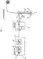
- FIG. 1 is a block diagram showing a high-frequency welding apparatus 100 according to Embodiment 1 of the present invention.
- the high-frequency welding device (continuous filling device) 100 includes a high-frequency output unit A, an impedance matching circuit unit E, and a cylindrical body manufacturing apparatus 1.
- the high frequency power output from the high frequency output unit A is supplied to the cylindrical body manufacturing apparatus 1 through the impedance matching circuit unit E.
- the to-be-welded material is high-frequency welded, and the welded cylindrical body is continuously filled with the contents.
- Each part which comprises the high frequency welding apparatus 100 is demonstrated in detail.
- the signal level of the high-frequency power has a peak at a frequency fc corresponding to the design frequency in the high-frequency output unit A described later, and the half-value width is 0.15 of the frequency fc. It is possible to realize an impedance matching circuit having a pass characteristic that is twice or more.
- the upper limit value of the half-value width of the pass characteristic does not define the invention described in the present specification, but the half-value width is 0.15 times or more and 0.26 times or less of the frequency fc as described later.
- a pass characteristic is realized. It will also be apparent to those skilled in the art who have come into contact with the present specification that a pass characteristic can be realized in which the upper limit value of the half width is about 0.30 times the frequency fc.
- FIG. 2 is a configuration diagram of the cylindrical body manufacturing apparatus 1 including the seal electrode 8a and the ground electrode 8b according to the first embodiment of the present invention.
- the cylindrical body manufacturing apparatus 1 is an apparatus that manufactures a cylindrical body for filling contents such as sausage or stick cheese. The cylindrical body manufacturing apparatus 1 will be described with reference to FIG.
- the top and bottom on the paper surface of FIG. 2 correspond to the top and bottom of the actual vertical direction, and the cylindrical body is sent so as to flow from top to bottom in the figure. That is, the upper side in the figure corresponds to the upstream side in the feeding direction of the cylindrical body in the filling operation, and the lower side in the figure corresponds to the downstream side in the feeding direction.
- a strip-shaped film (a material to be welded) F is supplied by the original film 2, the guide roller 3A, and the guide roller 3B.
- the film F is drawn out from the roll film 2 and guided by the guide roller 3 ⁇ / b> A and the guide roller 3 ⁇ / b> B and guided to the forming plate 6.
- the film F is preferably composed of a vinylidene chloride copolymer resin.
- the forming plate 6 has a cylindrical shape that opens up and down, and has a circumferential gap extending in the longitudinal direction at one place in the circumferential direction. Further, the upper end edge of the forming plate 6 is curved and inclined, and the film F is guided along the inner surface of the forming plate 6 to form a continuous cylindrical film F1 having an overlapping portion in which the side edges are overlapped. Is done.
- the guide tube 7 is suspended from the downstream side of the forming plate 6, and the continuous tubular film F1 is sent to the guide tube 7 while maintaining the tubular shape.
- the continuous tubular film F1 guided by the guide tube 7 is welded at the overlapping portion by a seal electrode 8a and a ground electrode 8b which are high-frequency electrodes for high-frequency welding.
- a pump 4 and a nozzle 5 for filling the formed continuous cylindrical film F1 with the contents C are provided on the upstream side of the forming plate 6, a pump 4 and a nozzle 5 for filling the formed continuous cylindrical film F1 with the contents C are provided.
- One end of the nozzle 5 is introduced into the guide tube 7, and the other end is connected to the pump 4.
- the tip of the nozzle 5 introduced into the guide tube 7 is opened downstream of the seal electrode 8a and the ground electrode 8b.
- the position of the pump 4 is not limited to the position above the forming plate 6, but may be disposed at another position where the contents C are easily replenished as appropriate, and connected to the nozzle 5 by piping.
- a feed roller 9a and a roller 9b as feed devices are provided on the downstream side of the guide tube 7 and the nozzle 5.
- the cylindrical body F2 filled with the contents C in the continuous cylindrical film F1 is continuously moved downward with the cylindrical bodies F2 being pressed downward with the pair of cylindrical feed rollers 9a and 9b pressing the contents C. Narrow pressure transport.
- cylindrical body F2 that has been transported under pressure is flattened by a squeezing device to form an absent portion where no content C is present.
- the cylindrical body F2 is closed by sealing or ligating the absent portion and cut into pieces by cutting with a cutter or the like.
- a high frequency power supply path that is a path for supplying high frequency power between the seal electrode 8a and the ground electrode 8b of the cylindrical body manufacturing apparatus 1 will be described.
- the high frequency power supply path is provided with a high frequency output section A and an impedance matching circuit section E.
- the high-frequency output unit A includes a crystal oscillation circuit A1 as a high-frequency oscillation circuit and a power amplification circuit A2 at the subsequent stage.
- the crystal oscillation circuit A1 is a circuit that transmits in synchronization with the natural frequency of the crystal resonator 11.
- an industrial scientific medical band (ISM band) frequency such as 13.56 MHz, 27.12 MHz, or 40.68 MHz is generally selected as a design frequency.
- a vibration element capable of generating a vibration having a natural frequency a SAW element using a surface acoustic wave, for example, is used in addition to the crystal resonator 11.
- the power amplification circuit A2 amplifies the high frequency output signal from the crystal oscillation circuit A1 to the power required for high frequency welding.
- the high frequency output signal amplified by the power amplifier circuit A2 is supplied to the impedance matching circuit E.
- the power amplifier circuit A2 a push-pull amplifier circuit using a known FET is preferably used.
- the impedance matching circuit portion E is a load (more precisely, the seal electrode 8a and the ground) that are formed by sandwiching the overlapping portion of the continuous tubular film F1 between the pair of welding seal electrodes 8a and the ground electrode 8b.
- the impedance matching is performed between the high frequency output unit A and a load circuit including the electrode 8b and the single wire feeder 16).
- the impedance matching circuit unit E is an L-type impedance matching circuit having an inductance element (coil) L and a variable capacitor Vc.
- the distance between the impedance matching circuit portion E, the seal electrode 8a, and the ground electrode 8b is the shortest distance allowed for device placement.
- the impedance matching circuit unit E since the installation position of the impedance matching circuit unit E is limited, the impedance matching circuit unit E must be of a size that can be installed at the position. Further, the impedance matching circuit portion E and the seal electrode 8a are connected by a single wire feeder 16. In this impedance matching circuit unit E, impedance matching adjustment is performed by adjusting the capacitance of the variable capacitor Vc.
- This impedance matching circuit section E has the following calculation formula according to the relationship between the Q value of the impedance matching circuit section E and the frequency f, where Zo is the output impedance of the power amplifier circuit A2 and Zi is the impedance due to the addition on the electrode side.
- the setting adjustment is performed as shown in FIG.
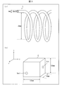
- FIG. 3 is an external view of the inductance element L and the impedance matching circuit unit E according to the first embodiment of the present invention
- (a) is an external view of the inductance element L.
- winding is pipe shape (the inside is a cavity).
- the winding is made of copper having an inner diameter of 2 mm and an outer diameter of 4 mm.
- the inner diameter of the inductance element L is 28 mm.
- the impedance matching circuit portion E according to the present invention includes a pipe-like coil.
- the impedance matching circuit unit E has a peak signal level of the high frequency power at a frequency (hereinafter also referred to as fc) corresponding to the design frequency in the high frequency output unit A, and a predetermined signal level (for example, a peak signal level). 12), an impedance matching circuit having a wider band than that of the conventional impedance matching circuit can be realized.
- FIG. 3B is an external view of the impedance matching circuit unit E.
- the impedance matching circuit section E is 80 mm in the direction perpendicular to the paper surface (hereinafter referred to as the x-axis direction) and the left-right direction of the paper surface (hereinafter referred to as the y-axis direction).
- a rectangular parallelepiped having a size of 120 mm in the vertical direction of the paper (hereinafter referred to as the z-axis direction).
- the impedance matching circuit unit E shown in FIG. 3B has an inductance element L and a variable capacitor Vc therein.
- the inductance element L according to the present invention has a pipe-like winding, so that the inside of the impedance matching circuit portion E can be easily formed by using an insulator (plastic) as a core. Can be fixed.
- the two windings must be fixed so as not to contact each other.
- the impedance matching circuit unit E may also vibrate when the vibration of the cylindrical body manufacturing apparatus 1 is transmitted, the two windings are fixed to the extent that they do not contact even when the impedance matching circuit unit E vibrates. Need to be done.
- the inductance element L according to the present invention can be installed inside the impedance matching circuit portion E having a limited size because the winding has a pipe shape.
- variable capacitor Vc of the impedance matching circuit unit E matches the output impedance Zo of the high-frequency output unit A and the impedance Zi on the electrode side, so that the cylindrical body manufacturing apparatus 1 can stack the continuous cylindrical film F1 most efficiently.
- the mating part can be welded.
- the impedance matching circuit unit E has a wider band at a predetermined signal level (for example, 1 ⁇ 2 of the peak signal level) than the pass characteristic of the conventional impedance matching circuit. Therefore, even when the speed of the continuous tubular film F1 changes and the impedance on the seal electrode 8a side fluctuates, signal level attenuation in the impedance matching circuit portion E is small, so control during operation is unnecessary. In other words, the impedance matching circuit portion E can stabilize the welding strength regardless of the speed of the continuous tubular film F1.
- a predetermined signal level for example, 1 ⁇ 2 of the peak signal level
- a vinylidene chloride resin film (Kurehalon, thickness 40 ⁇ m, width 80mm, manufactured by Kureha) is sandwiched between the electrodes, and the pass characteristics are measured using a network analyzer (Handheld RF combination analyzer Fieldfox N9914A) of Keysight Technologies. did. The measurement results are shown in FIG.
- FIG. 4 is a diagram showing measurement results in this example, (a) is a graph showing measurement results, and (b) is a table showing peak signals and half-value widths.
- the peak signal was higher when “TA26” was used than when “14T (4-2 pipe)” was used.
- “14T (4-2 pipe)” is wider than “TA26”. More specifically, when “TA26” is used, the full width at half maximum of 3.9 MHz is less than 0.15 times (about 0.14 times) the frequency 27.35 MHz at which the signal peaks.
- the half-value width of 5.8 MHz is 0.15 times or more (about 0.21 times) of 27.25 MHz where the signal peaks. For this reason, the impedance matching circuit unit using “14T (4-2 pipe)” can suppress the attenuation of the signal level even when the impedance on the seal electrode side fluctuates. It was possible to stabilize.
- an impedance matching circuit unit using an inductance element “14T (4-2 pipe)” and an impedance matching circuit unit using a conventional inductance element “TA26” are respectively provided. And welding was performed.
- 14T (4-2 pipe) is a copper coil in which a pipe-like winding having an inner diameter of 2 mm and an outer diameter of 4 mm is wound 14 times.
- TA26 is a copper coil in which a winding having a diameter of 2.6 mm is wound 15 times.
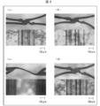
- FIG. 5 shows a photograph of a cross section and a photograph of the surface of the welded portion of the cylindrical body manufactured in this example.
- the upper side is a photograph of the cross section of the welded portion
- the lower side is a photograph of the surface of the welded portion.
- (A) to (d) of FIG. 5 are photographs of a cylindrical body manufactured under the following conditions.
- the surface and the cross section of the welded portion were the same as when “14T (4-2 pipe)” was used when the speed of the welded object was 36 m / min.
- the speed of the object to be welded is 15 m / min, the cross section of the welded portion is thin and the width of the weld on the surface is wide.
- the impedance matching circuit unit using “14T (4-2 pipe)” is a welded part even when the impedance on the seal electrode side fluctuates due to a change in the speed of the package body to be welded. Since the cross section and the surface of the steel plate did not change, the welding strength could be stabilized as compared with the conventional case.
- the pass characteristics of the impedance matching circuit section using the inductance elements “13T”, “14T”, and “15T” were measured with an automatic filling and packaging apparatus (KAP) manufactured by Kureha Co., Ltd.
- KAP automatic filling and packaging apparatus
- 13T is a copper coil in which a pipe-shaped winding having an inner diameter of 2 mm and an outer diameter of 4 mm is wound 13 times.
- 14T is a copper coil in which a pipe-like winding having an inner diameter of 2 mm and an outer diameter of 4 mm is wound 14 times.
- “15T” is a copper coil in which a pipe-like winding having an inner diameter of 2 mm and an outer diameter of 4 mm is wound 15 times.
- the welded material is moved at a speed of 20 m / min, 30 m / min, and 40 m / min while being cylindrical.
- the body was manufactured.
- the passage characteristics were measured in the same manner as in Example 1.
- the T-type peel strength of the welded portion of the welded material manufactured under each condition was measured according to JISJZ 0238: 1995, with the width of the test piece being 10 mm and the tensile speed being 200 mm / min. The measurement results are shown in FIG.
- FIG. 6 is a diagram showing the measurement results in this example, (a) is a graph showing the measurement results, and (b) is a table showing the T-type peel strength, the peak signal, and the half width. .
- the signal level is ⁇ 20 dB or more at 27.12 MHz that is the frequency of the ISM band, and in particular, ⁇ 18 dB at “14T”. It was the above signal level.
- the T-type peel strength of the welded portion was 1.80 kg / 10 mm or more regardless of the film speed in any of “13T”, “14T”, and “15T”.
- the T-type peel strength of the welded portion of the package filled with contents such as sausage or stick cheese is required to be 1.50 kg / 10 mm or more, sufficient T in any case. It can be said that it has mold release strength.
- “14T” produced a more stable welding strength because the T-type peel strength at the welded portion was 2.00 kg / 10 mm or more regardless of the film speed.
- the impedance matching circuit having a pipe-shaped coil with an inner diameter of 2 mm and an outer diameter of 4 mm has a full width at half maximum of 0.15 times the frequency fc at which the signal level is a peak. 0.30 times or less (more specifically, 0.26 times or less).
- the full width at half maximum was 0.21 or more times fc.
- the signal level was -18 dB or more at the ISM band frequency of 27.12 MHz.
- the impedance matching circuit had a T-type peel strength of 1.80 kg / 10 mm or more.
- the T-type peel strength was 2.00 kg / 10 mm or more. That is, the impedance matching circuit has produced a welding strength that is more stable than the conventional one.
- an impedance matching circuit includes a high-frequency electrode for high-frequency welding an object to be welded and a high-frequency output unit that supplies high-frequency power to the high-frequency electrode.
- the half width of the impedance matching circuit is not less than 0.15 times the frequency fc at which the signal level reaches its peak, the attenuation of the signal level is small with respect to the impedance variation at the high frequency electrode. Therefore, the welding strength in high frequency welding can be stabilized as compared with the conventional case.
- the impedance matching circuit may have a pass characteristic in which the half-value width is 0.21 or more times the frequency fc.
- the impedance matching circuit further suppresses the attenuation of the signal level with respect to the impedance variation in the high frequency electrode, the welding strength can be further stabilized.
- the signal level of the high frequency power may be ⁇ 18 dB or more at the design frequency in the high frequency output unit.
- the impedance matching circuit since the impedance matching circuit has little attenuation of the signal level at the design frequency in the high frequency output section, the high frequency power supplied from the high frequency output section can be reduced.
- the impedance matching circuit may include a coil whose winding is a pipe shape.
- the above-described impedance matching circuit can be easily realized.
- the impedance matching circuit is connected between a high-frequency electrode for high-frequency welding of an object to be welded and a high-frequency output unit that supplies high-frequency power to the high-frequency electrode.
- winding is provided with the coil which is pipe shape.
- the impedance matching circuit can reduce the attenuation of the signal level with respect to the impedance fluctuation in the high-frequency electrode, so that the welding strength can be stabilized.
- the impedance matching circuit can easily fix the coil, so that an impedance matching circuit strong against vibration can be realized. Can do.
- the said impedance matching circuit does not require the complicated structure for fixing a coil, it can suppress that the magnitude
- the winding of the coil may have an inner diameter of 2 mm and an outer diameter of 4 mm.
- the impedance matching circuit can further stabilize the welding strength.
- the number of turns of the coil may be 13 to 15 times.
- the impedance matching circuit can further stabilize the welding strength.
- a continuous filling device includes any one of the impedance matching circuits described above.
- a high-frequency welding apparatus includes any one of the impedance matching circuits described above.
- a continuous filling apparatus includes the above-described high-frequency welding apparatus, and the high-frequency welding apparatus winds one strip-shaped film into a cylindrical shape, and superimposes both side ends of the film to perform high-frequency welding. To do.
- the impedance matching circuit is a continuous filling device that continuously fills a cylindrical body that is welded by superimposing both side ends of a belt-like film by the high-frequency welding device. It is possible to realize a continuous filling device that produces the same effect as the above.
- the film may be a vinylidene chloride resin film.
- a cylindrical body for filling sausage or cheese can be provided.
- the present invention can be used for an impedance matching circuit connected between a high-frequency electrode for high-frequency welding of an object to be welded and a high-frequency output unit that supplies high-frequency power to the high-frequency electrode.
Landscapes
- Engineering & Computer Science (AREA)
- Life Sciences & Earth Sciences (AREA)
- Mechanical Engineering (AREA)
- Wood Science & Technology (AREA)
- Zoology (AREA)
- Food Science & Technology (AREA)
- Package Closures (AREA)
- Lining Or Joining Of Plastics Or The Like (AREA)
Abstract
高周波溶着において、溶着強度が安定する技術を提供する。筒状体(F2)を高周波溶着するためのシール電極(8a)と、シール電極およびアース電極(8b)の間に高周波電力を供給する高周波出力部(A)との間に接続され、高周波出力部における設計周波数に対応する周波数fcにおいて高周波電力の信号レベルがピークであり、半値幅が上記周波数fcの0.15倍以上となるような通過特性を有するインピーダンス整合回路(E)。
Description
本発明は、被溶着物を高周波溶着するための高周波電極と、当該高周波電極に高周波電力を供給する高周波出力部との間に接続されるインピーダンス整合回路、当該インピーダンス整合回路を備える高周波溶着装置、および当該高周波溶着装置を備える連続充填装置に関する。
ソーセージまたはスティックチーズ等の内容物が充填された包装体は、筒状に形成された筒状体に内容物を充填し、両端を結紮することによって製造されている。この筒状体は、1つの帯状のフィルムを筒状に巻き、当該フィルムの両側端部を重ね合わせて溶着することによって形成される。このようにフィルムを溶着する方法の一つである高周波溶着に関する技術が開発されている。
例えば、特許文献1には、高周波出力部からインピーダンス整合回路を介して一対の高周波電極間に高周波電力を供給し、この高周波電極に挟持されたフィルムの重畳部を高周波誘電加熱して溶着する高周波溶着装置が開示されている。当該高周波溶着装置は、一対の高周波電極の高圧側電極に容量的に結合される結合部と、この結合部から得られた信号を整流する整流回路とを有する検出回路を備えている。そして、当該検出回路は、高周波溶着装置の高周波電極に与えられる高周波電圧を検出する。特許文献1には、当該高周波溶着装置では、当該検出回路が検出した高周波電圧を監視しながらインピーダンス整合調整を行うことにより、高品質なフィルム包装体が得られると記載されている。
被溶着物を送りながら高周波溶着する高周波溶着装置の場合、当該高周波溶着装置が始動した直後は、被溶着物が送られる速度は遅く、そこから徐々に速度が上がり所定の速度に達する。しかしながら、従来技術では、被溶着物が送られる速度が遅い場合と速い場合とで溶着強度の変化が大きいため、溶着強度が安定しづらいという問題がある。
本発明は上記の課題に鑑みてなられたものであり、その目的は、高周波溶着において、従来に比べて溶着強度が安定する技術を提供することにある。
上記の課題を解決するために、本発明の一態様に係るインピーダンス整合回路は、被溶着物を高周波溶着するための高周波電極と、当該高周波電極に高周波電力を供給する高周波出力部との間に接続されるインピーダンス整合回路であって、上記高周波出力部における設計周波数に対応する周波数fcにおいて高周波電力の信号レベルがピークであり、半値幅が上記周波数fcの0.15倍以上となるような通過特性を有する。
さらに、本発明の一態様に係るインピーダンス整合回路においては、被溶着物を高周波溶着するための高周波電極と、当該高周波電極に高周波電力を供給する高周波出力部との間に接続されるインピーダンス整合回路であって、巻線がパイプ状であるコイルを備える。
本発明の一態様によれば、高周波溶着において、従来に比べて溶着強度が安定する技術を提供することができる。
以下、本発明の実施の形態について、詳細に説明する。
(高周波溶着装置100の構成)
図1は、本発明の実施形態1における高周波溶着装置100を示すブロック図である。高周波溶着装置(連続充填装置)100は、図1に示すように、高周波出力部A、インピーダンス整合回路部E、および筒状体製造装置1によって構成されている。高周波溶着装置100では、高周波出力部Aから出力される高周波電力がインピーダンス整合回路部Eを介して筒状体製造装置1に供給される。そして、筒状体製造装置1において、被溶着物が高周波溶着され、溶着された筒状体に内容物が連続充填される。高周波溶着装置100を構成する各部について、詳しく説明する。
図1は、本発明の実施形態1における高周波溶着装置100を示すブロック図である。高周波溶着装置(連続充填装置)100は、図1に示すように、高周波出力部A、インピーダンス整合回路部E、および筒状体製造装置1によって構成されている。高周波溶着装置100では、高周波出力部Aから出力される高周波電力がインピーダンス整合回路部Eを介して筒状体製造装置1に供給される。そして、筒状体製造装置1において、被溶着物が高周波溶着され、溶着された筒状体に内容物が連続充填される。高周波溶着装置100を構成する各部について、詳しく説明する。
以下のような構成を有する高周波溶着装置100によれば、後述する高周波出力部Aにおける設計周波数に対応する周波数fcにおいて高周波電力の信号レベルがピークであり、半値幅が上記周波数fcの0.15倍以上となるような通過特性を有するインピーダンス整合回路を実現することができる。
なお、通過特性の半値幅の上限値は、本明細書に記載の発明を規定するものではないが、後述するように、半値幅が上記周波数fcの0.15倍以上、0.26倍以下となるような通過特性が実現されている。また、本明細書に接した当業者であれば、半値幅の上限値が上記周波数fcの0.30倍程度となるような通過特性が実現できることも明らかであろう。
(筒状体製造装置1の構成)
図2は、本発明の実施形態1におけるシール電極8aおよびアース電極8bを備える筒状体製造装置1の構成図である。筒状体製造装置1は、ソーセージまたはスティックチーズ等の内容物を充填するための筒状体を製造する装置である。図2を参照して、筒状体製造装置1について説明する。
図2は、本発明の実施形態1におけるシール電極8aおよびアース電極8bを備える筒状体製造装置1の構成図である。筒状体製造装置1は、ソーセージまたはスティックチーズ等の内容物を充填するための筒状体を製造する装置である。図2を参照して、筒状体製造装置1について説明する。
図2の紙面上の上下は実際の鉛直方向の上下に対応し、筒状体は図中において上から下に流れるように送られる。すなわち、図中の上が充填作業における筒状体の送り方向の上流側に相当し、図中の下が送り方向の下流側に相当する。
筒状体製造装置1では、フィルム原反2、ガイドローラ3A、およびガイドローラ3Bにより、帯状のフィルム(被溶着物)Fが供給される。フィルムFは、ロール状にまかれたフィルム原反2から引き出され、ガイドローラ3Aおよびガイドローラ3Bに案内されて送られ、フォーミングプレート6に導かれる。フィルムFは、塩化ビニリデン系共重合体樹脂から構成されていることが好ましい。
フォーミングプレート6は、上下に開口する円筒形上を有しており周方向の一箇所において縦方向に延びる円周方向の隙間を有している。また、フォーミングプレート6の上端縁は湾曲傾斜しており、フィルムFは、フォーミングプレート6の内面に沿うように案内され、側縁同士を重ね合わせた重ね合わせ部を有する連続筒状フィルムF1が形成される。
フォーミングプレート6の下流側には案内筒7が垂下げられ、連続筒状フィルムF1は、筒状の形を保ったまま案内筒7へと送られる。案内筒7に案内された連続筒状フィルムF1は、高周波溶着するための高周波電極であるシール電極8aおよびアース電極8bによって重ね合わせ部を溶着される。
フォーミングプレート6の上流側には、形成された連続筒状フィルムF1に内容物Cを充填するポンプ4とノズル5とが設けられている。ノズル5は、一方の先端が案内筒7へ導入され、もう一方の先端がポンプ4に接続されている。案内筒7へ導入されたノズル5の先端は、シール電極8aおよびアース電極8bより下流側において開口している。なお、ポンプ4の位置は、フォーミングプレート6の上方に限定されず、内容物Cを適宜補充し易い他の位置に配置され、配管によってノズル5に接続されてもよい。
案内筒7およびノズル5の下流側に、送り装置である送りローラ9aおよびローラ9bが設けられている。連続筒状フィルムF1内に内容物Cが充填された筒状体F2を、一対の円柱状の送りローラ9aおよびローラ9bが内容物Cを押圧した状態で筒状体F2を下方へ連続して狭圧搬送する。
なお、挟圧搬送された筒状体F2は、しごき装置によって扁平されることにより内容物Cが存在しない不在部が形成される。筒状体F2は、この不在部を封止したり結紮したりして閉じ、カッター等で切断することにより、包装体に個片化される。
(高周波電力供給経路)
筒状体製造装置1のシール電極8aおよびアース電極8bの間に高周波電力を供給する経路である高周波電力供給経路について説明する。高周波電力供給経路には、高周波出力部Aおよびインピーダンス整合回路部Eが設けられている。
筒状体製造装置1のシール電極8aおよびアース電極8bの間に高周波電力を供給する経路である高周波電力供給経路について説明する。高周波電力供給経路には、高周波出力部Aおよびインピーダンス整合回路部Eが設けられている。
高周波出力部Aには、高周波発振回路としての水晶発振回路A1と、その後段の電力増幅回路A2とが含まれている。水晶発振回路A1は、水晶振動子11の固有振動数に同調して発信する回路である。水晶振動子11の固有振動数としては、13.56MHz、27.12MHz、または40.68MHzなど、産業科学医療用バンド(ISMバンド)の周波数が一般に設計周波数として選ばれる。固有振動数の振動を発生し得る振動素子としては、水晶振動子11の他に、例えば表面弾性波を使用したSAW素子などが使用される。
電力増幅回路A2は、水晶発振回路A1からの高周波出力信号を、高周波溶着に必要となる電力にまで増幅する。電力増幅回路A2によって増幅された高周波出力信号は、インピーダンス整合回路Eに供給される。電力増幅回路A2としては、公知のFETを使用したプッシュプル増幅回路が好適に使用される。
インピーダンス整合回路部Eは、一対の溶着用のシール電極8aおよびアース電極8bの間に連続筒状フィルムF1の重ね合わせ部が挟持されることに基づく負荷(より正確には、シール電極8aおよびアース電極8bや単線給電線16を含む負荷回路)と高周波出力部Aとの間のインピーダンス整合を行うものである。インイーダンス整合回路部Eは、インダクタンス素子(コイル)Lと可変コンデンサVcとを有するL型インピーダンス整合回路である。インピーダンス整合回路部Eと、シール電極8aおよびアース電極8bとの間隔は、機器配置に際して許される最短の距離とされている。そのため、インピーダンス整合回路部Eは設置位置が限定されるため、インピーダンス整合回路部Eは当該位置において設置可能な大きさでなければならない。また、インピーダンス整合回路部Eとシール電極8aとの間は単線給電線16により接続される。このインピーダンス整合回路部Eでは、可変コンデンサVcのキャパシタンスを調整することにより、インピーダンス整合調整が行われる。
このインピーダンス整合回路部Eは、電力増幅回路A2の出力インピーダンスをZo、電極側の付加によるインピーダンスをZiとしたとき、インピーダンス整合回路部EのQ値および周波数fとの関係により、以下の計算式に示す通りの設定調整を行うものである。

続いて、インピーダンス整合回路部のインダクタンス素子Lについて、図3を用いて詳しく説明する。図3は、本発明の実施形態1におけるインダクタンス素子Lおよびインピーダンス整合回路部Eの外観図であり、(a)は、インダクタンス素子Lの外観図である。図3の(a)に示すように、インダクタンス素子Lは、巻線がパイプ状(内部が空洞)である。また、巻線は、内径が2mm、外径が4mmの銅製である。また、インダクタンス素子Lの内径は28mmである。このように、本発明におけるインピーダンス整合回路部Eは巻線がパイプ状のコイルを備えている。そのため、インピーダンス整合回路部Eは、高周波出力部Aにおける設計周波数に対応する周波数(以下、fcとも称する)において高周波電力の信号レベルがピークであり、所定の信号レベル(例えば、ピークの信号レベルの12)における帯域が、従来のインピーダンス整合回路の通過特性に比べて広いインピーダンス整合回路を実現できる。
図3の(b)は、インピーダンス整合回路部Eの外観図である。図3の(b)に示すように、インピーダンス整合回路部Eは、紙面に対して垂直な方向(以下、x軸方向と称する)に80mm、紙面の左右方向(以下、y軸方向と称する)に135mm、紙面の上下方向(以下、z軸方向と称する)に120mmの大きさの直方体を有している。図3の(b)に示すインピーダンス整合回路部Eは、その内部にインダクタンス素子Lと可変コンデンサVcとを有している。また、図3の(b)に示すインピーダンス整合回路部Eは、高周波出力部A側に接続される入力端子Ein、およびシール電極8a側に接続される出力端子Eoutを有している。また、本発明におけるインダクタンス素子Lは、図3の(a)に示すように、巻線がパイプ状のため、絶縁体(プラスチック)を芯にすることにより、容易にインピーダンス整合回路部Eの内部において固定することができる。
一方、例えば、インダクタンス素子Lと同じ特性を持つインダクタンス素子を、内部に空洞を有しない巻線2本を用いて実現した場合、当該2本の巻線は接触しないように固定されなければならない。また、筒状体製造装置1の振動が伝わることによりインピーダンス整合回路部Eも振動する場合があるため、当該2本の巻線は、インピーダンス整合回路部Eが振動しても接触しない程度に固定される必要がある。しかしながら、上述したように、インピーダンス整合回路部Eは、その大きさが限られているため、複雑な構成を用いてインダクタンス素子を固定することはできない。一方、本発明におけるインダクタンス素子Lは、巻線がパイプ状であるため、限られた大きさのインピーダンス整合回路部Eの内部に設置することが可能となる。
(高周波溶着装置100の初期調整)
高周波溶着装置100の初期調整について説明する。
高周波溶着装置100の初期調整について説明する。
(1)シール電極8aとアース電極8bとの間に連続筒状フィルムF1の重ね合わせ部を挟み、ローラ9aおよびローラ9bを駆動して、連続筒状フィルムF1を下方向へ連続送りする。
(2)インピーダンス整合回路部Eの可変コンデンサVcによって、高周波出力部Aの出力インピーダンスZoと電極側のインピーダンスZiとが整合され、筒状体製造装置1が最も効率よく連続筒状フィルムF1の重ね合わせ部を溶着することができる。
(運転時)
上述したように、インピーダンス整合回路部Eは、所定の信号レベル(例えば、ピークの信号レベルの1/2)における帯域が、従来のインピーダンス整合回路の通過特性に比べて広い。そのため、連続筒状フィルムF1の速度が変わり、シール電極8a側のインピーダンスが変動しても、インピーダンス整合回路部Eにおける信号レベルの減衰が少ないため、運転時の制御は不要である。換言すると、インピーダンス整合回路部Eは、連続筒状フィルムF1の速度に関わらず、溶着強度を安定させることができる。
上述したように、インピーダンス整合回路部Eは、所定の信号レベル(例えば、ピークの信号レベルの1/2)における帯域が、従来のインピーダンス整合回路の通過特性に比べて広い。そのため、連続筒状フィルムF1の速度が変わり、シール電極8a側のインピーダンスが変動しても、インピーダンス整合回路部Eにおける信号レベルの減衰が少ないため、運転時の制御は不要である。換言すると、インピーダンス整合回路部Eは、連続筒状フィルムF1の速度に関わらず、溶着強度を安定させることができる。
本発明は上述した上記実施形態に限定されるものではなく、請求項に示した範囲で種々の変更が可能であり、開示された技術的手段を適宜組み合わせて得られる実施形態についても本発明の技術的範囲に含まれる。
以下、実施例を挙げて本発明をさらに詳しく説明するが、本発明はその要旨を超えない限り、これら実施例に限定されるものではない。
(実施例1)
本発明の一実施例について図4に基づいて説明すれば以下のとおりである。
本発明の一実施例について図4に基づいて説明すれば以下のとおりである。
クレハ社製の自動充填包装装置(KAP)にて、インダクタンス素子「14T(4-2パイプ)」を用いたインピーダンス整合回路部、および従来のインダクタンス素子「TA26」を用いたインピーダンス整合回路部の通過特性をそれぞれ測定した。具体的には、「14T(4-2パイプ)」は、内径2mm、外径4mmのパイプ状の巻線を14回巻いた銅製のコイルである。また、「TA26」は、直径2.6mmの巻線を15回巻いた銅製のコイルである。そして、塩化ビニリデン系樹脂フィルム(クレハロン、厚さ40μm、幅80mm、クレハ社製)を電極間に挟み、キーサイトテクノロジーズ社のネットワークアナライザー(ハンドヘルドRFコンビネーションアナライザFieldfox N9914A)を用いて、通過特性を測定した。測定結果を、図4に示す。
図4は、本実施例における測定結果を示す図であり、(a)は、測定結果を示すグラフであり、(b)は、ピーク信号と半値幅とを示す表である。
図4に示すように、ピーク信号は、「TA26」を用いた場合の方が、「14T(4-2パイプ)」を用いた場合と比べて、高くなっていた。しかしながら、信号レベルが6dB減衰する帯域(半値幅)は、「14T(4-2パイプ)」の方が「TA26」よりも広くなっていた。より具体的には、「TA26」を用いた場合、半値幅3.9MHzは、信号がピークとなる周波数27.35MHzの0.15倍未満(約0.14倍)である。一方、「14T(4-2パイプ)」を用いた場合、半値幅5.8MHzは、信号がピークになる27.25MHzの0.15倍以上(約0.21倍)である。そのため、「14T(4-2パイプ)」を用いたインピーダンス整合回路部は、シール電極側のインピーダンスが変動した場合であっても、信号レベルの減衰を抑制できるため、従来に比べて溶着強度を安定させることができた。
(実施例2)
本発明の他の実施例について、図5に基づいて説明すれば、以下のとおりである。
本発明の他の実施例について、図5に基づいて説明すれば、以下のとおりである。
クレハ社製の自動充填包装装置(KAP)にて、インダクタンス素子「14T(4-2パイプ)」を用いたインピーダンス整合回路部、および従来のインダクタンス素子「TA26」を用いたインピーダンス整合回路部をそれぞれ用いて、溶着を行った。具体的には、「14T(4-2パイプ)」は、内径2mm、外径4mmのパイプ状の巻線を14回巻いた銅製のコイルである。また、「TA26」は、直径2.6mmの巻線を15回巻いた銅製のコイルである。そして、塩化ビニリデン系樹脂フィルム(クレハロン、厚さ40μm、幅80mm、クレハ社製)を使用して、被溶着物を15m/分、36m/分のそれぞれの速度で動かしながら筒状体を製造し、溶着部の表面および断面の写真を撮影した。撮影した写真を、図5に示す。
図5は、本実施例において製造した筒状体の溶着部の断面の写真および表面の写真である。図5の(a)から(d)はそれぞれ、上側が溶着部の断面の写真、下側が溶着部の表面の写真である。図5の(a)から(d)はそれぞれ、以下の条件にて製造された筒状体の写真である。
(a)「14T(4-2パイプ)」を用いて、被溶着物を15m/分の速度で動かしながら製造した筒状体
(b)「14T(4-2パイプ)」を用いて、被溶着物を36m/分の速度で動かしながら製造した筒状体
(c)「TA26」を用いて、被溶着物を15m/分の速度で動かしながら製造した筒状体
(d)「TA26」を用いて、被溶着物を36m/分の速度で動かしながら製造した筒状体
図5に示すように、「14T(4-2パイプ)」を用いた場合、被溶着物の速度が15m/分であっても36m/分であっても、溶着部の表面および断面に違いはほとんどなかった。一方、「TA26」を用いると、被溶着物の速度が36m/分の場合は、「14T(4-2パイプ)」を用いた場合と変わらない溶着部の表面および断面であった。しかしながら、被溶着物の速度が15m/分の場合は、溶着部の断面は厚さが薄くなり、また表面における溶着の幅も広くなっていた。このように、「14T(4-2パイプ)」を用いたインピーダンス整合回路部は、被溶着物である包装体の速度の変化によってシール電極側のインピーダンスが変動した場合であっても、溶着部の断面および表面は変わらないため、従来に比べて溶着強度を安定させることができた。
(b)「14T(4-2パイプ)」を用いて、被溶着物を36m/分の速度で動かしながら製造した筒状体
(c)「TA26」を用いて、被溶着物を15m/分の速度で動かしながら製造した筒状体
(d)「TA26」を用いて、被溶着物を36m/分の速度で動かしながら製造した筒状体
図5に示すように、「14T(4-2パイプ)」を用いた場合、被溶着物の速度が15m/分であっても36m/分であっても、溶着部の表面および断面に違いはほとんどなかった。一方、「TA26」を用いると、被溶着物の速度が36m/分の場合は、「14T(4-2パイプ)」を用いた場合と変わらない溶着部の表面および断面であった。しかしながら、被溶着物の速度が15m/分の場合は、溶着部の断面は厚さが薄くなり、また表面における溶着の幅も広くなっていた。このように、「14T(4-2パイプ)」を用いたインピーダンス整合回路部は、被溶着物である包装体の速度の変化によってシール電極側のインピーダンスが変動した場合であっても、溶着部の断面および表面は変わらないため、従来に比べて溶着強度を安定させることができた。
(実施例3)
本発明のさらに他の実施例について、図6に基づいて説明すれば、以下のとおりである。
本発明のさらに他の実施例について、図6に基づいて説明すれば、以下のとおりである。
クレハ社製の自動充填包装装置(KAP)にて、インダクタンス素子「13T」、「14T」、および「15T」を用いたインピーダンス整合回路部の通過特性をそれぞれ測定した。具体的には、「13T」は、内径2mm、外径4mmのパイプ状の巻線を13回巻いた銅製のコイルである。また、「14T」は、内径2mm、外径4mmのパイプ状の巻線を14回巻いた銅製のコイルである。また、「15T」は、内径2mm、外径4mmのパイプ状の巻線を15回巻いた銅製のコイルである。そして、塩化ビニリデン系樹脂フィルム(クレハロン、厚さ40μm、幅80mm、クレハ社製)を使用して、被溶着物を20m/分、30m/分、40m/分のそれぞれの速度で動かしながら筒状体を製造した。また、実施例1と同様に通過特性を測定した。そして、それぞれの条件において製造された被溶着物の溶着部分のT型剥離強度を、JIS Z 0238:1995に準じて、試験片の幅を10mm、引張速度を200mm/分として、測定した。測定結果を、図6に示す。
図6は、本実施例における測定結果を示す図であり、(a)は、測定結果を示すグラフであり、(b)は、T型剥離強度、ピーク信号、および半値幅を示す表である。
「13T」、「14T」、および「15T」のそれぞれにおいて、信号レベルがピークになる周波数fcは、以下の値であった。
13T:27.65MHz
14T:27.25MHz
15T:26.95MHz
したがって、「13T」、「14T」、および「15T」の何れにおいても、半値幅は、信号レベルがピークになる周波数fcの0.15倍以上、0.30倍以下(より具体的には、0.26倍以下)であった。特に、「13T」および「14T」は、半値幅が、信号レベルがピークになる周波数fcの0.21倍以上であった。
14T:27.25MHz
15T:26.95MHz
したがって、「13T」、「14T」、および「15T」の何れにおいても、半値幅は、信号レベルがピークになる周波数fcの0.15倍以上、0.30倍以下(より具体的には、0.26倍以下)であった。特に、「13T」および「14T」は、半値幅が、信号レベルがピークになる周波数fcの0.21倍以上であった。
また、「13T」、「14T」、および「15T」の何れの場合においても、ISMバンドの周波数である27.12MHzでは、-20dB以上の信号レベルであり、特に、「14T」では、-18dB以上の信号レベルであった。
また、溶着部分のT型剥離強度は、「13T」、「14T」、および「15T」の何れにおいても、フィルム速度に関わらず1.80kg/10mm以上であった。一般的に、ソーセージまたはスティックチーズ等の内容物が充填された包装体の溶着部分のT型剥離強度は1.50kg/10mm以上が求められている実情を鑑みると、何れの場合も十分なT型剥離強度を有していると言える。特に、「14T」は、フィルム速度に関わらず、溶着部分のT型剥離強度は2.00kg/10mm以上であるため、より安定した溶着強度を生み出していた。
このように、上述の実施例では、巻線が内径2mm、外径4mmのパイプ状であるコイルを有するインピーダンス整合回路は、半値幅が、信号レベルがピークである周波数fcの0.15倍以上、0.30倍以下(より具体的には、0.26倍以下)であった。特に、コイルの巻線を13回または14回巻いた場合、半値幅はfcの0.21倍以上であった。さらに、コイルの巻線を14回巻いた場合、ISMバンドの周波数である27.12MHzでは、-18dB以上の信号レベルであった。そして、当該インピーダンス整合回路は、フィルム速度が20m/分、30m/分、40m/分と変化しても、T型剥離強度が1.80kg/10mm以上であった。特に、コイルの巻線を14回巻いた場合、T型剥離強度は2.00kg/10mm以上であった。すなわち、当該インピーダンス整合回路は、従来に比べて安定した溶着強度を生み出していた。
[付記事項]
[付記事項]
上記の課題を解決するために、本発明の一態様に係るインピーダンス整合回路は、被溶着物を高周波溶着するための高周波電極と、当該高周波電極に高周波電力を供給する高周波出力部との間に接続されるインピーダンス整合回路であって、上記高周波出力部における設計周波数に対応する周波数fcにおいて高周波電力の信号レベルがピークであり、半値幅が上記周波数fcの0.15倍以上となるような通過特性を有する。
上記の構成によれば、インピーダンス整合回路は、半値幅が、信号レベルがピークとなる周波数fcの0.15倍以上であるため、高周波電極におけるインピーダンスの変動に対して信号レベルの減衰が少ない。そのため、高周波溶着における溶着強度を従来に比べて安定させることができる。
さらに、本発明の一態様に係るインピーダンス整合回路においては、半値幅が上記周波数fcの0.21倍以上となる通過特性を有していてもよい。
上記の構成によれば、インピーダンス整合回路は、高周波電極におけるインピーダンスの変動に対する信号レベルの減衰をより抑制するため、溶着強度をより安定させることができる。
さらに、本発明の一態様に係るインピーダンス整合回路においては、上記高周波出力部における設計周波数において、高周波電力の信号レベルが-18dB以上であってもよい。
上記の構成によれば、インピーダンス整合回路は、高周波出力部における設計周波数において信号レベルの減衰が少ないため、高周波出力部が供給する高周波電力を小さくすることができる。
さらに、本発明の一態様に係るインピーダンス整合回路においては、巻線がパイプ状であるコイルを備えていてもよい。
上記の構成によれば、上述したインピーダンス整合回路を容易に実現することができる。
さらに、本発明の一態様に係るインピーダンス整合回路においては、被溶着物を高周波溶着するための高周波電極と、当該高周波電極に高周波電力を供給する高周波出力部との間に接続されるインピーダンス整合回路であって、巻線がパイプ状であるコイルを備える。
上記の構成によれば、インピーダンス整合回路は、高周波電極におけるインピーダンスの変動に対して、信号レベルの減衰を少なくできるため、溶着強度を安定させることができる。
また、同じ特性を有するコイルを2本の巻線によって実現した場合に比べて、上記インピーダンス整合回路は、コイルを容易に固定することができるため、振動に対して強いインピーダンス整合回路を実現することができる。また、上記インピーダンス整合回路は、コイルを固定するための複雑な構造が不要なので、インピーダンス整合回路の大きさが大きくなることを抑制することができる。
さらに、本発明の一態様に係るインピーダンス整合回路においては、上記コイルの巻線は、内径が2mm、外径が4mmであってもよい。
上記の構成によれば、インピーダンス整合回路は、溶着強度をより安定させることができる。
さらに、本発明の一態様に係るインピーダンス整合回路においては、上記コイルの巻き数は13回~15回であってもよい。
上記の構成によれば、インピーダンス整合回路は、溶着強度をより安定させることができる。
さらに、本発明の一態様に係る連続充填装置は、上記いずれかに記載のインピーダンス整合回路を備える。
上記の構成によれば、上記のインピーダンス整合回路と同じ効果を奏する連続充填装置を実現することができる。
さらに、本発明の一態様に係る高周波溶着装置は、上記いずれかに記載のインピーダンス整合回路を備える。
上記の構成によれば、上記のインピーダンス整合回路と同じ効果を奏する高周波溶着装置を実現することができる。
さらに、本発明の一態様に係る連続充填装置は、上記高周波溶着装置を備え、上記高周波溶着装置は、1つの帯状のフィルムを筒状に巻き、当該フィルムの両側端部を重ね合わせて高周波溶着する。
上記の構成によれば、上記高周波溶着装置によって帯状のフィルムの両側端部を重ね合わせて溶着された筒状体に連続して内容物を充填する連続充填装置であって、上記のインピーダンス整合回路と同じ効果を奏する連続充填装置を実現することができる。
さらに、本発明の一態様に係る連続充填装置においては、上記フィルムは、塩化ビニリデン系樹脂フィルムであってもよい。
上記の構成によれば、ソーセージまたはチーズ等を充填するための筒状体を提供することができる。
本発明は、被溶着物を高周波溶着するための高周波電極と、当該高周波電極に高周波電力を供給する高周波出力部との間に接続されるインピーダンス整合回路に利用することができる。
1 筒状体製造装置
8a シール電極
8b アース電極
100 高周波溶着装置
A 高周波出力部
E インピーダンス整合回路部
L インダクタンス素子
Vc 可変コンデンサ
8a シール電極
8b アース電極
100 高周波溶着装置
A 高周波出力部
E インピーダンス整合回路部
L インダクタンス素子
Vc 可変コンデンサ
Claims (10)
- 被溶着物を高周波溶着するための高周波電極と、当該高周波電極に高周波電力を供給する高周波出力部との間に接続されるインピーダンス整合回路であって、
上記高周波出力部における設計周波数に対応する周波数fcにおいて高周波電力の信号レベルがピークであり、半値幅が上記周波数fcの0.15倍以上となるような通過特性を有するインピーダンス整合回路。 - 半値幅が上記周波数fcの0.21倍以上となる通過特性を有する請求項1に記載のインピーダンス整合回路。
- 上記高周波出力部における設計周波数において、高周波電力の信号レベルが-18dB以上であることを特徴とする請求項1または2に記載のインピーダンス整合回路。
- 巻線がパイプ状であるコイルを備えていることを特徴とする請求項1~3の何れか1項に記載のインピーダンス整合回路。
- 被溶着物を高周波溶着するための高周波電極と、当該高周波電極に高周波電力を供給する高周波出力部との間に接続されるインピーダンス整合回路であって、巻線がパイプ状であるコイルを備えることを特徴とするインピーダンス整合回路。
- 上記コイルの巻線は、内径が2mm、外径が4mmであることを特徴とする請求項5に記載のインピーダンス整合回路。
- 上記コイルの巻き数は13回~15回であることを特徴とする請求項5または6に記載のインピーダンス整合回路。
- 請求項1~7のいずれか1項に記載のインピーダンス整合回路を備えることを特徴とする高周波溶着装置。
- 請求項8に記載の高周波溶着装置を備え、
上記高周波溶着装置は、1つの帯状のフィルムを筒状に巻き、当該フィルムの両側端部を重ね合わせて高周波溶着することを特徴とする連続充填装置。 - 上記フィルムは、塩化ビニリデン系樹脂フィルムであることを特徴とする請求項9に記載の連続充填装置。
Priority Applications (2)
| Application Number | Priority Date | Filing Date | Title |
|---|---|---|---|
| JP2017514058A JP6534735B2 (ja) | 2015-04-23 | 2016-04-06 | インピーダンス整合回路、高周波溶着装置および連続充填装置 |
| CN201680025301.7A CN107531348B (zh) | 2015-04-23 | 2016-04-06 | 阻抗匹配电路、高频熔接装置以及连续填充装置 |
Applications Claiming Priority (2)
| Application Number | Priority Date | Filing Date | Title |
|---|---|---|---|
| JP2015-088347 | 2015-04-23 | ||
| JP2015088347 | 2015-04-23 |
Publications (1)
| Publication Number | Publication Date |
|---|---|
| WO2016170985A1 true WO2016170985A1 (ja) | 2016-10-27 |
Family
ID=57144346
Family Applications (1)
| Application Number | Title | Priority Date | Filing Date |
|---|---|---|---|
| PCT/JP2016/061282 Ceased WO2016170985A1 (ja) | 2015-04-23 | 2016-04-06 | インピーダンス整合回路、高周波溶着装置および連続充填装置 |
Country Status (3)
| Country | Link |
|---|---|
| JP (1) | JP6534735B2 (ja) |
| CN (1) | CN107531348B (ja) |
| WO (1) | WO2016170985A1 (ja) |
Citations (4)
| Publication number | Priority date | Publication date | Assignee | Title |
|---|---|---|---|---|
| JPS5232785B2 (ja) * | 1973-10-30 | 1977-08-24 | ||
| JPH06238754A (ja) * | 1993-02-17 | 1994-08-30 | Kureha Chem Ind Co Ltd | 高周波溶着装置およびこれを用いたフィルム包装装置 |
| JPH1119945A (ja) * | 1997-07-07 | 1999-01-26 | Bridgestone Corp | 加硫金型の清浄方法 |
| JP2014101534A (ja) * | 2012-11-16 | 2014-06-05 | Nippon Steel & Sumitomo Metal | 後熱処理装置 |
Family Cites Families (4)
| Publication number | Priority date | Publication date | Assignee | Title |
|---|---|---|---|---|
| JPH0720039B2 (ja) * | 1991-03-28 | 1995-03-06 | 株式会社芝浦製作所 | 高周波インピ−ダンス整合回路 |
| KR0151231B1 (ko) * | 1993-02-17 | 1998-10-15 | 고다마 순이치로오 | 고주파 용착장치 및 이를 사용한 필름 포장장치 |
| CN1817622A (zh) * | 2006-03-13 | 2006-08-16 | 方先其 | 高频熔接聚乙烯阀口袋的方法及专用屏蔽板 |
| CN101754509A (zh) * | 2008-12-17 | 2010-06-23 | 陈建 | 程序控制高频熔接机运行的方法及电路 |
-
2016
- 2016-04-06 WO PCT/JP2016/061282 patent/WO2016170985A1/ja not_active Ceased
- 2016-04-06 JP JP2017514058A patent/JP6534735B2/ja active Active
- 2016-04-06 CN CN201680025301.7A patent/CN107531348B/zh active Active
Patent Citations (4)
| Publication number | Priority date | Publication date | Assignee | Title |
|---|---|---|---|---|
| JPS5232785B2 (ja) * | 1973-10-30 | 1977-08-24 | ||
| JPH06238754A (ja) * | 1993-02-17 | 1994-08-30 | Kureha Chem Ind Co Ltd | 高周波溶着装置およびこれを用いたフィルム包装装置 |
| JPH1119945A (ja) * | 1997-07-07 | 1999-01-26 | Bridgestone Corp | 加硫金型の清浄方法 |
| JP2014101534A (ja) * | 2012-11-16 | 2014-06-05 | Nippon Steel & Sumitomo Metal | 後熱処理装置 |
Non-Patent Citations (1)
| Title |
|---|
| YOSHIHIRO KONISHI: "Micro-ha Kairo no Kiso to sono Oyo", SOGO DENSHI SHUPPANSHA, vol. 119, no. third edition, 10 June 1995 (1995-06-10), pages 159 - 164 * |
Also Published As
| Publication number | Publication date |
|---|---|
| CN107531348B (zh) | 2019-12-27 |
| JP6534735B2 (ja) | 2019-06-26 |
| JPWO2016170985A1 (ja) | 2018-02-08 |
| CN107531348A (zh) | 2018-01-02 |
Similar Documents
| Publication | Publication Date | Title |
|---|---|---|
| JP5293498B2 (ja) | ウエブ搬送装置及びその方法と電池の製造方法 | |
| US20100012764A1 (en) | Apparatus and Method for Winding Film Onto a Film Roll | |
| CN105686073A (zh) | 烟草加工工业的双层的管子以及用于制造这样的管子的装置和方法 | |
| JP6853735B2 (ja) | 巻回装置 | |
| CN108685162B (zh) | 用于制造烟草加工业的至少双层管状的条的方法及用于制造烟草加工业的至少双层条的装置 | |
| JP2013541430A (ja) | 開封が簡単な袋状体 | |
| AU2016237239B2 (en) | Bag-making machine | |
| CN108371342B (zh) | 用于制造烟草加工业的条的方法以及条成形装置 | |
| JP4778414B2 (ja) | バッグの製造方法 | |
| EP3727042A1 (en) | Method and unit for crimping a web of material for the tobacco industry | |
| US10843833B2 (en) | Device for sealing a packaging | |
| CN103597327A (zh) | 用于计算超声焊头的振动幅度的方法 | |
| US7484347B2 (en) | Packaging filling apparatus and transversal sealing apparatus | |
| WO2016170985A1 (ja) | インピーダンス整合回路、高周波溶着装置および連続充填装置 | |
| CN110277532A (zh) | 二次电池集流体的加工方法及加工设备 | |
| US7488398B2 (en) | Method for changing rolls of tubular film | |
| AU2002362357B2 (en) | Method for controlling the position of a foil strip edges | |
| KR20180066032A (ko) | 권취된 시트의 보빈을 권출하는 방법 및 보빈을 권출하기 위한 권출 장치 | |
| CN101971271A (zh) | 具有斜边缘接头的管形双金属内层的同轴电缆及其方法 | |
| CN103895891A (zh) | 筒状体制造装置 | |
| JP2024500201A (ja) | 誘導加熱シール装置 | |
| US11780200B2 (en) | Device and method for producing at least one empty open bag | |
| JP6326220B2 (ja) | 包装機械におけるチューブ状包材の位置ずれ監視装置 | |
| KR102319915B1 (ko) | 금속으로 튜브를 제조하는 방법 | |
| CN103978676B (zh) | 用于生产充气床垫中的充气柱体配件的自动压拉带机 |
Legal Events
| Date | Code | Title | Description |
|---|---|---|---|
| 121 | Ep: the epo has been informed by wipo that ep was designated in this application |
Ref document number: 16783006 Country of ref document: EP Kind code of ref document: A1 |
|
| ENP | Entry into the national phase |
Ref document number: 2017514058 Country of ref document: JP Kind code of ref document: A |
|
| NENP | Non-entry into the national phase |
Ref country code: DE |
|
| 122 | Ep: pct application non-entry in european phase |
Ref document number: 16783006 Country of ref document: EP Kind code of ref document: A1 |